Embed Size (px)
Citation preview
http://dx.doi.org/10.5573/JSTS.2015.15.1.096 JOURNAL OF SEMICONDUCTOR TECHNOLOGY AND SCIENCE, VOL.15, NO.1, FEBRUARY, 2015
Manuscript received Jun. 9, 2014; accepted Nov. 13, 2014 1 College of Information & Communication Engineering, Sungkyunkwan University, Suwon, Korea 2 Samsung Electronics, Hwasung, Korea E-mail : [email protected]
Adaptive Digital Background Gain Mismatch Calibration for Multi-lane High-speed Serial Links
Hyun-Wook Lim1, Bai-Sun Kong1, and Young-Hyun Jun2
Abstract—Adaptive background gain calibration loop for multi-lane serial links is proposed. In order to detect and cancel gain mismatches between lanes, a single digital loop using a SD ADC is employed, which provides a real-time adaptation of gain variations and is shared among all lanes to reduce power and area. Evaluation result showed that gain mismatches between lanes were well calibrated and tracked, resulting in timing budget at 10-6 BER increased from 0.261 UI to 0.363 UI with stable loop convergence. Index Terms—Gain mismatch calibration, source-synchronous, sigma-delta modulator
I. INTRODUCTION
As more functionalities are integrated in mobile devices, data transfer rate and power consumption in a mobile device has been increasing. So, a critical issue in mobile system design is to use a high-speed interface with least power consumption. A well known technique is to use the multi-lane low-swing transceiver [1]. But, it suffers from a small amplitude margin due to lane-dependent signal attenuation and from a small timing margin due to timing skew caused by gain mismatch among lanes, which indicates that a highly accurate gain calibration is required. To address the issue, analog gain mismatch calibration loops were proposed [2, 3]. But, they are not adequate for multi-lane applications because the loop should be implemented separately for each lane,
resulting in substantial increase on power consumption and area as the number of lane increases. These analog loops are also not adequate for low power because analog circuits should always be turned on to hold calibrated gain values. Since analog loops are sensitive to intersymbol interference of received data as well as to power supply noise, a preamble or training pattern should be used, implying that the gain mismatches caused by dynamic temperature and voltage variations cannot be tracked.
To overcome these problems, this brief proposes an adaptive digital background gain mismatch calibration loop based on sigma-delta ADC for use in multi-lane low-swing receivers. Section II describes the proposed gain calibration loop. Comparison results are presented in Section III. Conclusions are given in Section IV.
II. PROPOSED DIGITAL GAIN CALIBRATION
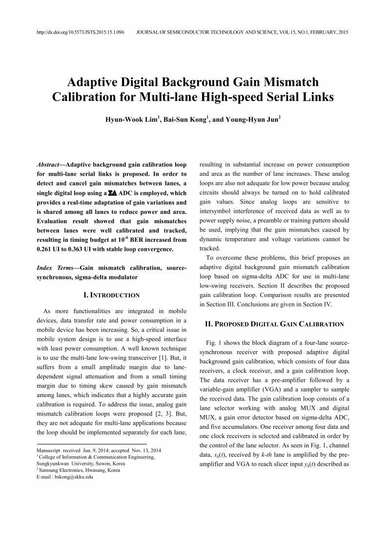
Fig. 1 shows the block diagram of a four-lane source-synchronous receiver with proposed adaptive digital background gain calibration, which consists of four data receivers, a clock receiver, and a gain calibration loop. The data receiver has a pre-amplifier followed by a variable-gain amplifier (VGA) and a sampler to sample the received data. The gain calibration loop consists of a lane selector working with analog MUX and digital MUX, a gain error detector based on sigma-delta ADC, and five accumulators. One receiver among four data and one clock receivers is selected and calibrated in order by the control of the lane selector. As seen in Fig. 1, channel data, xk(t), received by k-th lane is amplified by the pre-amplifier and VGA to reach slicer input yk(t) described as
JOURNAL OF SEMICONDUCTOR TECHNOLOGY AND SCIENCE, VOL.15, NO.1, FEBRUARY, 2015 97
( ) { ( ) ( )} ( )1 2y t g g gc t g t x tk k k k= × + + D × (1)
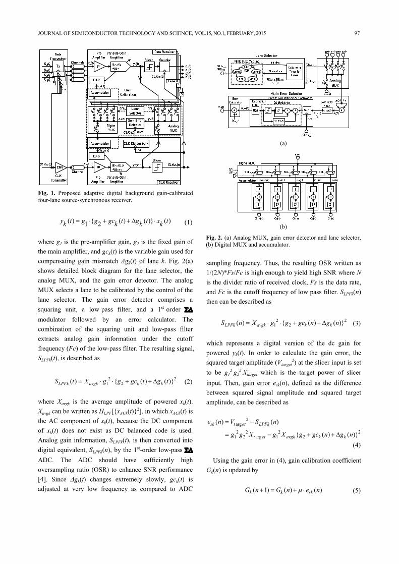
where g1 is the pre-amplifier gain, g2 is the fixed gain of the main amplifier, and gck(t) is the variable gain used for compensating gain mismatch Δgk(t) of lane k. Fig. 2(a) shows detailed block diagram for the lane selector, the analog MUX, and the gain error detector. The analog MUX selects a lane to be calibrated by the control of the lane selector. The gain error detector comprises a squaring unit, a low-pass filter, and a 1st-order SD modulator followed by an error calculator. The combination of the squaring unit and low-pass filter extracts analog gain information under the cutoff frequency (Fc) of the low-pass filter. The resulting signal, SLPFk(t), is described as
2 21 2( ) { ( ) ( )}LPFk avgk k kS t X g g gc t g t= × × + + D (2)
where Xavgk is the average amplitude of powered xk(t). Xavgk can be written as HLPF[{xACk(t)}2], in which xACk(t) is the AC component of xk(t), because the DC component of xk(t) does not exist as DC balanced code is used. Analog gain information, SLPFk(t), is then converted into digital equivalent, SLPFk(n), by the 1st-order low-pass SD ADC. The ADC should have sufficiently high oversampling ratio (OSR) to enhance SNR performance [4]. Since Δgk(t) changes extremely slowly, gck(t) is adjusted at very low frequency as compared to ADC
sampling frequency. Thus, the resulting OSR written as 1/(2N)*Fs/Fc is high enough to yield high SNR where N is the divider ratio of received clock, Fs is the data rate, and Fc is the cutoff frequency of low pass filter. SLPFk(n) then can be described as
2 21 2( ) { ( ) ( )}LPFk avgk k kS n X g g gc n g n= × × + + D (3)
which represents a digital version of the dc gain for powered yk(t). In order to calculate the gain error, the squared target amplitude (Vtarget
2) at the slicer input is set to be g1
2·g2
2·Xtarget which is the target power of slicer
input. Then, gain error esk(n), defined as the difference between squared signal amplitude and squared target amplitude, can be described as
2
arg
2 2 2 21 2 arg 1 2
( ) ( )
{ ( ) ( )}sk t et LPFk
t et avgk k k
e n V S n
g g X g X g gc n g n
= -
= - + + D
(4) Using the gain error in (4), gain calibration coefficient
Gk(n) is updated by
( 1) ( ) ( )k k skG n G n e nm+ = + × (5)
Fig. 1. Proposed adaptive digital background gain-calibrated four-lane source-synchronous receiver.
(a)
+ + + + +
(b)
Fig. 2. (a) Analog MUX, gain error detector and lane selector, (b) Digital MUX and accumulator.

98 HYUN-WOOK LIM et al : ADAPTIVE DIGITAL BACKGROUND GAIN MISMATCH CALIBRATION FOR MULTI-LANE …
where μ is a step value of the gain loop, and the adaptation is based on the RMS feedback algorithm [5]. In Fig. 2(b), the digital MUX selects a lane to be updated, and Gk(n) is updated until esk(n) reaches the minimum value. As a result, the gain of each channel converges to the optimum value, and the receiver latency variation among channels will be minimized.
III. PERFORMANCE EVALUATION
The proposed gain calibration loop is well suited for multi-lane application since single calibration loop is shared by all lanes in a time-multiplexed manner, resulting in substantial power and area reduction. The power consumption can be further reduced by turning the circuits off for the period in which the calibration is not being done. Another merit of having a single loop is that probable mismatches among calibration circuits in the conventional scheme do not exist, improving calibration accuracy. Moreover, by adopting a SD modulator with noise shaping, the proposed scheme allows an accurate calibration for slowly varying quantities like receiver gain without being affected by noise sources including the quantization noise. Use of the low-frequency gain extractor working with DC-balanced code and the time- shared digital loop allow the proposed scheme to be well suited for background calibration. Since the loop operates at very low frequency with no disturbance on data receiving operation, a reliable multi-lane data reception with higher data rate can be achieved.
To assess the performance of the proposed scheme, the entire receiver system was modeled using MATLAB and SIMULINK with design parameters listed in Table 1. The gain and bandwidth mismatch values used for the evaluation were determined by considering the variation of the process technology. After the standard deviations of pre- and main-amplifier gain variations were found from the process data, the standard deviation of the overall amplifier gain variation was estimated. Then, by applying the Normal Distribution Function having this standard deviation for each of the data and clock lanes, the overall gain mismatch was found to be within ±15%. By the same method, the bandwidth deviation from the nominal bandwidth value was found to be within ±8%. The reason for having a lower mismatch for the bandwidth is that the bandwidth mismatch of the pre- and
main-amplifier pair is determined by that of a single amplifier having narrower bandwidth whereas the gain mismatch is determined by the gain variations of both the pre- and main-amplifiers. Monte-Carlo simulation was performed to check the convergence of receiver gain and to measure BER before and after calibration with amplifier dc gain and 3 dB bandwidth mismatches randomly assigned to all lanes. The simulation results are shown in Fig. 3, where Fig. 3(a) shows gain coefficients migration during calibration, indicating a good
Table 1. Evaluation Environment Parameter Value
Data transfer rate 3.125 Gbps Input amplitude, Vpp 17 mV
Input SNR 12 dB Pre- and main amplifier gain 4.0 V/V, 9.0 V/V±15%
Pre- and main amplifier bandwidth 2.1875 GHz±8% Detector LPF cutoff frequency 100 KHz
SHA clock frequency 15.625 MHz DSM oversampling ratio 156.25 Effective Number of Bit 8.42 bit Target amplitude, Vtarget 0.5 V
Decision amplitude ±1.0 V Step for gain LMS loop, μ 2-9
Gain DAC full scale 8 V/V DAC resolution 5 bit
(a) (d)
(b) (c)
Fig. 3. (a) Convergence of gain coefficients; cumulative eye diagrams with jitter histograms, (b) before, (c) after calibration, (d) bathtub curves before and after calibration.
JOURNAL OF SEMICONDUCTOR TECHNOLOGY AND SCIENCE, VOL.15, NO.1, FEBRUARY, 2015 99
convergence of lane receiver gain values. Fig. 3(b) and (c) show eye diagrams and jitter histograms at slicer input before and after calibration, where four eyes (for four lanes) are all combined together, resulting in a substantial reduction of timing skew. Fig. 3(d) shows bathtub curves, where the timing budget at 10-6 BER was enhanced from 0.261 UI to 0.363 UI in 12 dB AWGN channel model, indicating 39% improvement. Table 2 shows the performance summary of calibration loops, which shows that, since the proposed scheme requires just a single calibration loop for N-lane receiver, an ever larger amounts of power and area saving can be achieved as the number of lanes increases.
IV. CONCLUSIONS
This paper presents a digital calibration loop based on sigma-delta ADC for multi-lane receivers. The proposed calibration loop can provide an improved BER with reduced power and area.
ACKNOWLEDGMENTS
This work was supported by Samsung Electronics and the Basic Research Program through the National Research Foundation of Korea funded by the Ministry of Education under Grant 2013R1A1A2A10009535 and by the Ministry of Education, Science, and Technology under Grant 2010-0013702. Design tools were supported by IDEC, KAIST.
REFERENCES
[1] R. Palmer, et al, “Design considerations for low-power high-performance mobile logic and memory
interfaces,” in IEEE ASSCC, pp. 205–208, 2008. [2] I.-H. Wang and S.-I. Liu, “A 0.18- CMOS 1.25-
Gbps Automatic-Gain-Control Amplifier,” IEEE TCAS-II, vol. 55, no. 2, pp. 136–140, 2008.
[3] O. Jeon, et al, “Analog AGC circuitry for CMOS WLAN receiver,” IEEE JSSC, vol.41, no.10, pp. 2291–2300, Oct. 2000.
[4] J. Rosa, “Sigma-delta modulator: tutorial overview, design guide, and state-of-the-art survey,” IEEE TCAS-I, vol.58, no.1, pp.1–21, Jan. 2011.
[5] G. N. Tavares, et al, “High performance algorithms for digital signal processing AGC,” in IEEE ISCAS, vol.2, pp. 1529–1532, 1990.
Hyun-Wook Lim received the B.S. and M.S. degrees in Electrical Engineering from Korea University, Korea, in 1996 and 1998. He joined Samsung Electronics, Korea, in 1998, where he has been involved in DRAM and display interface design.
He is currently working toward the PhD. degree in Semiconductor and Display Engineering from Sungkyunkwan University.
Bai-Sun Kong received the B.S. degree in electronics engineering from Yonsei University, Seoul, Korea, in 1990, and the M.S. and the Ph.D. degrees in electrical engineering from Korea Advanced Institute of Science and Technology (KAIST),
Taejon, Korea, in 1992 and 1996, respectively. From 1996 to 1999 he was with LG Semicon (currently Hynix Semiconductor), Seoul, Korea, as a senior design engineer, where he was working on the design of high-density and high-bandwidth DRAMs. In 2000, he joined the faculty of Korea Aerospace University, Goyang, Korea, as an assistant professor at the School of Electronics Telecommunication and Computer Engineering. In 2005, he moved to Sungkyunkwan University, Suwon, Korea, where he is currently a professor at the College of Information and Communication Engineering. His research interests include high-performance microprocessor/ memory architecture/circuit designs, high-speed I/O interface design, and IC designs for low-power/high-speed applications.
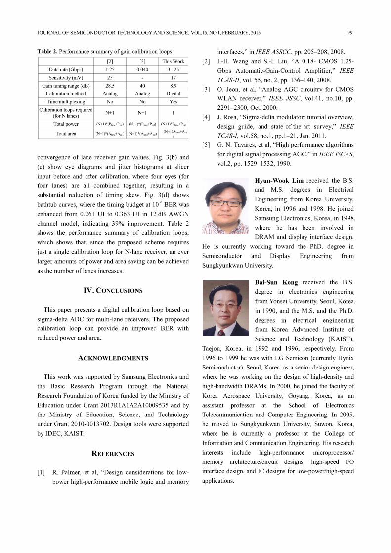
Table 2. Performance summary of gain calibration loops [2] [3] This Work
Data rate (Gbps) 1.25 0.040 3.125 Sensitivity (mV) 25 - 17
Gain tuning range (dB) 28.5 40 8.9 Calibration method Analog Analog Digital Time multiplexing No No Yes
Calibration loops required (for N lanes) N+1 N+1 1
Total power (N+1)*(Plane+Pcal) (N+1)*(Plane+Pcal) (N+1)*Plane+Pcal
Total area (N+1)*(Alane+Acal) (N+1)*(Alane+Acal) (N+1)Alane+Aca
l
100 HYUN-WOOK LIM et al : ADAPTIVE DIGITAL BACKGROUND GAIN MISMATCH CALIBRATION FOR MULTI-LANE …
Young-Hyun Jun received the M.S. and Ph.D. degrees in electrical engineering from the Korea Advanced Institute of Science and Technology (KAIST), Seoul, in 1986 and 1989, respectively. From 1989 to 1991, he was with the Coordinated
Science Laboratory, University of Illinois at Urbana-Champaign as a Research Associate, where he was working on the design of analog circuits. Since 2014, he has been working as the President of the Memory Business division in Samsung Electronics, Korea. He has published many technical papers and holds many patents related to semiconductor design. His research interests are in the development of high-speed DRAMs and I/O interface, flash memories, low-power VLSI circuits, and various analog circuit designs.