Embed Size (px)
Citation preview

Symposia on VLSI Technology and Circuits
Adaptive Robustness Tuning for High
Performance Domino Logic
Bharan Giridhar1, David Fick1,
Matthew Fojtik1, Sudhir Satpathy1, David Bull2,
Dennis Sylvester1 and David Blaauw1
1University of Michigan, USA
2ARM, United Kingdom
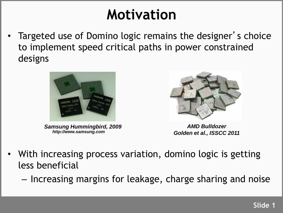
Motivation
• Targeted use of Domino logic remains the designer’s choice
to implement speed critical paths in power constrained
designs
• With increasing process variation, domino logic is getting
less beneficial
– Increasing margins for leakage, charge sharing and noise
Slide 1
http://www.samsung.com AMD Bulldozer
Golden et al., ISSCC 2011
Samsung Hummingbird, 2009

Motivation
• Margining the keeper for robustness under worst-
case PVT can degrade performance by ~32%
• ART Domino tracks PVT and trades extra robustness
and timing margins for performance
Slide 2
Nominal Process Process,
Temp
Process,
Temp,
Noise
0.77
1.00
1.23
1.46 Normalized Delay
Normalized Keeper Size
No
rmali
zed
Dela
y
1
4
7
10
No
rmali
zed
Keep
er
Siz
e
~32% perform
ance degradation
A0 A1
CLK
VDD
VSS
VDD
VSS
VDD
VSS
Keeper Margining

ART Domino Gate
• Fast, speculative evaluation followed by fully
margined (safe) evaluation to detect errors
Slide 3
A B
CLK
VSS
VSS
VDD
VSS
VDD
VSS
VDD VDD
VSS VSS

ART Domino Gate
• Fast, speculative evaluation followed by fully
margined (safe) evaluation to detect errors
Slide 4
A B
CLK
VDD
VSSVSS
VSS
VDD
VSS
VDD
VSS

ART Domino Gate
• Fast, speculative evaluation followed by fully
margined (safe) evaluation to detect errors
Slide 5
Headers/footers shared across gates to minimize overhead
CLK
SPEC
CHECK
(SPECB)
Sp
ec
ula
tiv
e
Pre
ch
arg
e (
SP
)
Sp
ec
ula
tiv
e
Ev
alu
ati
on
(S
E)
Ch
ec
ke
r
Pre
ch
arg
e
(CP
)
Ch
ec
ke
r
Ev
alu
ati
on
(CE
)
A
VDYN
Y
VX
VY
A B
CLK
VX
VY
VDD TVDD
SPEC SPECB
VSS
VSS
VDD
TVSS ( ≥ VSS)VSS
SPECB SPEC
VSS
VDD
VSS

A B
CLK
VX(<VDD)
VY(>VSS)
VDD TVDD
SPEC SPECB
VSS
VSS
VDD
TVSS ( ≥ VSS)VSS
SPECB SPEC
VSS
VDD
VSS
Leakier
Stack
ART Domino Gate
• VX < VDD and VY > VSS speed critical transitions at both
nodes by reducing voltage swings
• VY > VSS speeds the following gate by trading its noise
margin for speed
Slide 6
CLK
SPEC
CHECK
(SPECB)
Sp
ec
ula
tiv
e
Pre
ch
arg
e (
SP
)
Sp
ec
ula
tiv
e
Ev
alu
ati
on
(S
E)
Ch
ec
ke
r
Pre
ch
arg
e
(CP
)
Ch
ec
ke
r
Ev
alu
ati
on
(CE
)
A
VDYN
Y
VX
VY
Remove margins

ART Domino Gate
• VX < VDD and VY > VSS speed critical transitions at both
nodes by reducing voltage swings
• VY > VSS speeds the following gate by trading its noise
margin for speed
Slide 7
Fast, speculative evaluation
CLK
SPEC
CHECK
(SPECB)
Sp
ec
ula
tiv
e
Pre
ch
arg
e (
SP
)
Sp
ec
ula
tiv
e
Ev
alu
ati
on
(S
E)
Ch
ec
ke
r
Pre
ch
arg
e
(CP
)
Ch
ec
ke
r
Ev
alu
ati
on
(CE
)
A
VDYN
Y
VX
VY
Y (Speculate)
A B
CLK
VX(<VDD)
VY(>VSS)
VDD TVDD
SPEC SPECB
VSS
VSS
VDD
TVSS ( ≥ VSS)VSS
SPECB SPEC
VSS
VDD
VSS
Leakier
Stack

ART Domino Gate
• Slower, safe evaluation performed in the background
– No impact on computation latency
Slide 8
CLK
SPEC
CHECK
(SPECB)
Sp
ec
ula
tiv
e
Pre
ch
arg
e (
SP
)
Sp
ec
ula
tiv
e
Ev
alu
ati
on
(S
E)
Ch
ec
ke
r
Pre
ch
arg
e
(CP
)
Ch
ec
ke
r
Ev
alu
ati
on
(CE
)
A
VDYN
Y
VX
VY
Restore margins
A B
CLK
VX(=VDD)
VY(=VSS)
VDD TVDD
SPEC SPECB
VSS
VSS
VDD
TVSS ( ≥ VSS)VSS
SPECB SPEC
VSS
VDD
VSS
Leakier
Stack
Y (Speculate)
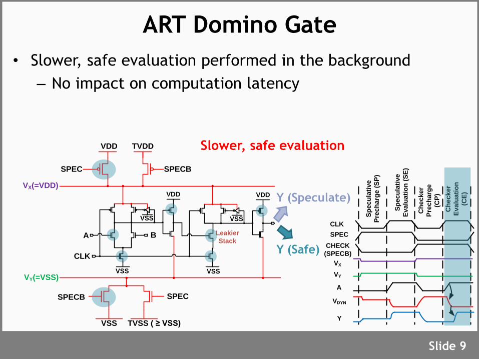
ART Domino Gate
• Slower, safe evaluation performed in the background
– No impact on computation latency
Slide 9
CLK
SPEC
CHECK
(SPECB)
Sp
ec
ula
tiv
e
Pre
ch
arg
e (
SP
)
Sp
ec
ula
tiv
e
Ev
alu
ati
on
(S
E)
Ch
ec
ke
r
Pre
ch
arg
e
(CP
)
Ch
ec
ke
r
Ev
alu
ati
on
(CE
)
A
VDYN
Y
VX
VY
Slower, safe evaluation
Y (Safe)
A B
CLK
VX(=VDD)
VY(=VSS)
VDD TVDD
SPEC SPECB
VSS
VSS
VDD
TVSS ( ≥ VSS)VSS
SPECB SPEC
VSS
VDD
VSS
Leakier
Stack
Y (Speculate)

ART Domino Gate
• In case of errors, the errant computation is flushed from the
pipeline
– The result of safe evaluation is propagated, guaranteeing
forward progress
Slide 10
Error Detection
Compare
and
Detect
Errors
Y (Safe)
A B
CLK
VX
VY
VDD TVDD
SPEC SPECB
VSS
VSS
VDD
TVSS ( ≥ VSS)VSS
SPECB SPEC
VSS
VDD
VSS
Y (Speculate)
Slide 11
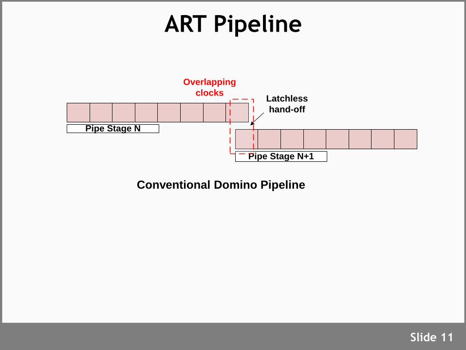
ART Pipeline
Pipe Stage N
Pipe Stage N+1
Overlapping
clocksLatchless
hand-off
Conventional Domino Pipeline

Slide 12
ART Pipeline
Pipe Stage N
Pipe Stage N+1

Slide 13
ART Pipeline
DO
MB
UF
Pipe Stage N
DO
MB
UF
Pipe Stage N+1
B
U
F
1B
U
F
1
M
U
XM
U
X
X
X

• During SE, DOMBUF snoops on the value propagated
forward through the mux
• Overlapping clocks eliminate latches between pipe
stages, provide skew tolerance
Slide 14
ART Pipeline
DO
MB
UF
Pipe Stage N
DO
MB
UF
Pipe Stage N+1
B
U
F
1B
U
F
1
Speculative Evaluation
(SE)
Stores speculative result
of half-stage
M
U
XM
U
X
Latchless
hand-off
Overlapping
clocks

• During SE, DOMBUF snoops on the value propagated
forward through the mux
• Overlapping clocks eliminate latches between pipe
stages, provide skew tolerance
Slide 15
ART Pipeline
Overlapping
clocksDO
MB
UF
Pipe Stage N
DO
MB
UF
Pipe Stage N+1
B
U
F
1Latchless
hand-off
B
U
F
1
Speculative Evaluation
(SE)
Stores speculative result
of half-stage
M
U
XM
U
X

• To allow the slower safe evaluation to complete,
each pipe stage is split in half during CE
• Value stored on DOMBUF propagated forward
cutting the stage depth by half
Slide 16
ART Pipeline
DO
MB
UF
Pipe Stage N
DO
MB
UF
Pipe Stage N+1
M
U
X
B
U
F
1Latchless
hand-off
Checking Evaluation
(CE)
Pipe-stage Split: Parallel
evaluations during CE
phase
DOMBUF value from
SE propagated B
U
F
1
M
U
X

ART Pipeline
• Both halves of each pipe stage perform safe
evaluations simultaneously
Slide 17
DO
MB
UF
Pipe Stage N
DO
MB
UF
Pipe Stage N+1
M
U
X
B
U
F
1Latchless
hand-off
Checking Evaluation
(CE)B
U
F
1
M
U
X
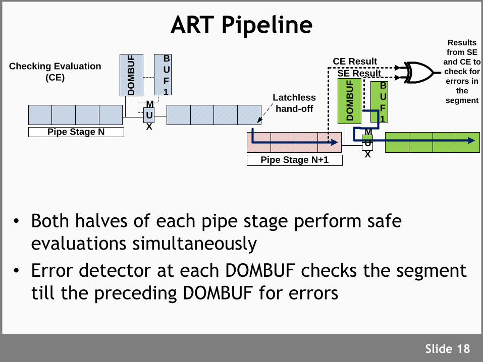
• Both halves of each pipe stage perform safe
evaluations simultaneously
• Error detector at each DOMBUF checks the segment
till the preceding DOMBUF for errors
Slide 18
ART Pipeline
DO
MB
UF
Pipe Stage N
DO
MB
UF
Pipe Stage N+1
M
U
X
B
U
F
1Latchless
hand-off
Checking Evaluation
(CE)
CE Result
SE Result
Results
from SE
and CE to
check for
errors in
the
segment
B
U
F
1
M
U
X

ART Pipeline
• CP: Precharge error logic (in red)
• CE: Copy Gate4 TO BUF2 and DOMBUF to BUF1
• SP+SE: Evaluate Domino XOR, Domino OR tree
Slide 19
Error Detection
SE SECP CE SP
SYSCLK
STG_1
Stage_1
error
Error Detection in next clock cycle in
parallel with next set of gate evaluations
DO
MB
UF
GA
TE
1
GA
TE
2
GA
TE
3
GA
TE
4
GA
TE
5
GA
TE
6
GA
TE
7
GA
TE
8
ErrorBIT0
Pipe Stage N
Stage_N
error
Bit0
Bit1
BitN
BUF1
BUF2 (identical to BUF1)
Fully margined
Domino XOR
Fully Margined
Domino OR tree

A0 A1
STG_N
VX
VY
SIG_SP_N
SIG_SE_NSIG_SPB_N
VSS
VS
S
VDD
VSS
VDD
SPEC_N
BUF1
VSS VSS
BUFIN
BUFOUT
SPECB_N
VD
D
ART Pipeline
Slide 20
A0 A1
STG_N+1
VX
VY
VDD TVDD
SPEC_N+1 SPECB_N+1
VSS
VSS
VDD
TVSS ( ≥ VSS)VSS
SPECB_N+1 SPEC_N+1
DO
MB
UF
Pipe Stage N
DO
MB
UF
Pipe Stage N+1
B
U
F
1B
U
F
1
M
U
XM
U
X
DOMBUF,
BUF1(2) are
fully
margined

ART Clock Generation
Slide 21
Ф1 (= STG_N)
Ф2 ( = STG_N+1)
GCLK
( from clock ring)
CK
D Q
RN
QN
SN
CK
D Q
RN
QN
SN
CK
D Q
RN
QN
SN
GCLK Ф1 Ф2
Ф3 ( = SPEC_N)
Ф4 ( = SPEC_N+1)
Power gates and other locally derived signals
clocked using locally generated clocks
Domino gates clocked by the global clock generator
SPEC_N
STG_NSIG_SE_N
SPECB_N
STG_NSIG_CE_N
STG_NSIG_SP_N
SPECB_N
STG_NSIG_CP_N
SPEC_N
SE
SE
SE
SE
CP
CP
CE
CE
SP
SPSP
STG_1
STG_2

System Implementation
• 32×32b multiplier in 65nm CMOS
• 4 TVDD/TVSS voltage domains, 2 pipeline stages
Slide 22
X[15:0] BOOTH
ENCODER
NEG[15:0]SHIFT[15:0]
ZERO[15:0]
PARTIAL
PRODUCTS[15:0][32:0]
SIGN[15:0]
RADIX-2 KOGGE
STONE
A[63:0]
PRODUCT[63:0]
BOOTH
DECODER
MULTIPLIER
ARRAY
Y[15:0]
TEST HARNESS
(TVDD2,TVSS2)
(TVDD3,TVSS3)
(TVDD1,TVSS1)
(TVDD4,TVSS4)
Pipe Stage 1 Pipe Stage 2
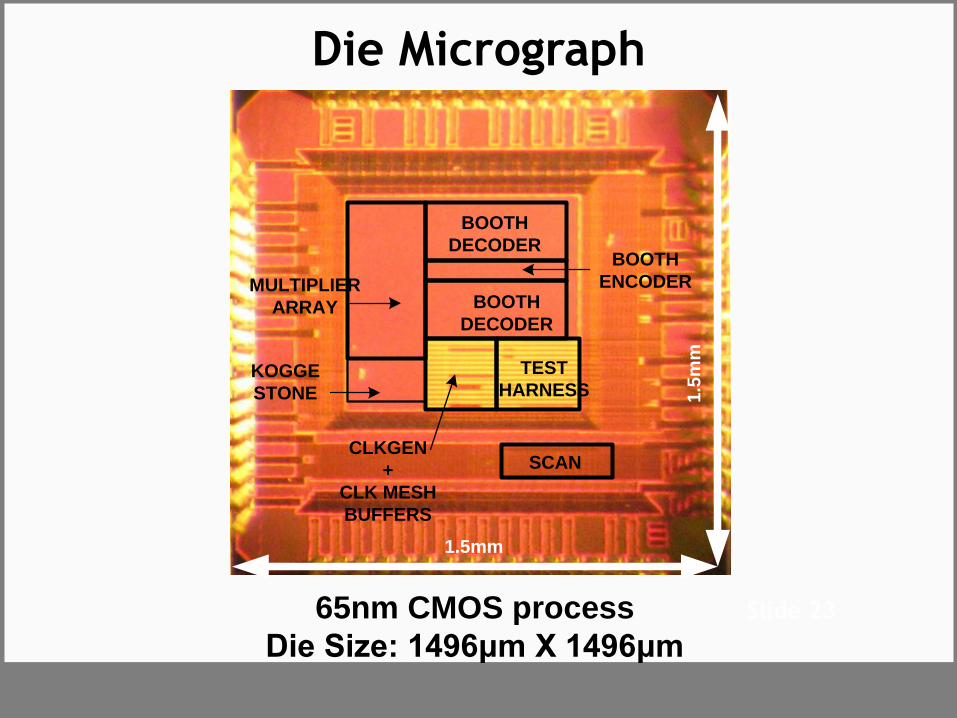
Die Micrograph
Slide 23
TEST
HARNESS
SCANCLKGEN
+
CLK MESH
BUFFERS
MULTIPLIER
ARRAY
KOGGE
STONE
BOOTH
DECODER
BOOTH
DECODER
BOOTH
ENCODER
1.5
mm
1.5mm
65nm CMOS process
Die Size: 1496μm X 1496μm

Measured Results
Slide 24
Performance with
ART up by 34% by
eliminating
robustness margins
at nominal PVT
912 MHz
944 MHz
976 MHz1008 MHz
1040 MHz 1072 MHz1104 MHz
1136 MHz
0.00 0.05 0.10 0.15 0.200.0
0.1
0.2
0.3
1.2
-TV
DD
(V
)
TVSS (V)
No Adapting
890 MHz
Error region (Robustness failure)
Measured Max. Performance: 1192 MHz

Measured Results
• Method applicable to performance constrained logic where
performance cannot be obtained by any other means
• Power increases sharply at higher frequencies due to increased
short circuit current on the output inverter
Slide 25
850 900 950 1000 1050 1100 1150 1200
0.00
0.05
0.10
0.15
0.20
0.25
0.30
TVDD1, TVDD
2, TVDD
3, TVDD
4
Req
uir
ed
TV
DD
(V
)
Performance (MHz)
850 900 950 1000 1050 1100 1150 1200
0.00
0.05
0.10
0.15
0.20
0.25
TVSS4
TVSS1, TVSS
2, TVSS
3
Req
uir
ed
T
VS
S (
V)
Performance (MHz)
Minimum Power at each
frequency
ΔTVDD/ΔTVSS at each measured
power-frequency point
850 900 950 1000 1050 1100 1150 1200
100
150
200
250
300
Simulated Power
Standard Domino
~17% Performance gain with
12% Power reduction
Performance (MHz)
Po
we
r (m
W)
No Adapting
~34% performance gain with
47% Power increase

ART Performance Gain
• Measured average % gain due to robustness tuning
across 20 dies is ~28%
• % Gain decreases at higher temperatures as gates
become less robust
Slide 26
22 24 26 28 30 32 34 36 38 400
2
4
6
8
10
Nu
mb
er
of
Ch
ips
% Performance Gain
(Robustness Speculation)
At 27C, 1.2V VDD
20 30 40 50 60 70 80 90
20
25
30
35
40
% P
erf
orm
an
ce
Ga
in
(Ro
bu
stn
es
s s
pe
cu
lati
on
)
Temperature (C)
Slow Die
Fast Die
Typical Die
20 Dies

Overall Performance Gain
Slide 27
Total gains of 49% to 71%
over conventionally
margined designs
Slow Nominal Fast300
400
500
600
700
800
900
1000
1100
1200
1300
1.67X
1.33X
1.17X
1.12X
1.71X
1.28X
1.12X
1X
1.49X
1.2X
698
698
698
Pe
rfo
rma
nc
e (
MH
z)
Worst Process,Voltage,Temp* Process Gain
Temp Gain Voltage Gain ART Gain
31
698
4885
3937108
105108
201
302241
1038
1192 1169
1.04X1.07X
* Worst process was set by the slowest die. Temperature
was set to 85C and Supply was degraded by 10% to 1.08V
Robustness
tuning
Process gain
Temp gain
Voltage gain
ART gain
Timing
Speculation

Error Rate
• Error rate is more sensitive to TVSS than TVDD
– TVSS tuning also affects robustness of following gate
Slide 28
0.00 0.01 0.02 0.03 0.04 0.05
0
20
40
60
80
100
% E
rro
r (r
ob
us
tne
ss
fa
ilu
res
)
TVDD
(V), TVSS
(V)*
TVDD tuning
TVSS tuning
1192 MHz
TVDD1-4
= 0.9V
TVSS1-3
= 0.15V, TVSS4 = 0.17V
880 890 900 910 920 930 940 950 960 970
-5
0
5
10
15
20
25
30
35
40
% E
rro
r (t
imin
g f
ailu
res
)
Operating Frequency (MHz)
TVDD[1-4] = 1.2V
TVSS[1-4] = 0V
* ΔTVDD = 0.9V-TVDD,
ΔTVSS = TVSS-0.17V

Conclusion
• A new high speed design style called ART Domino
was presented
• ART Domino provides overall gain of up to 1.71x
over conventional domino
– 3.2x faster than static CMOS
• Design overhead is amortized over pipeline stage
depth
Slide 29

Thank You
Slide 30
Questions?

Symposia on VLSI Technology and Circuits
BACKUP SLIDES
Slide 31

ART Clock Generation
Slide 32
Ф1 (= STG_N)
Ф2 ( = STG_N+1)
GCLK
( from clock ring)
CK
D Q
RN
QN
SN
CK
D Q
RN
QN
SN
CK
D Q
RN
QN
SN
GCLK Ф1 Ф2
Ф3 ( = SPEC_N)
Ф4 ( = SPEC_N+1)
Locally generated clocking signals with stricter
skew constraints
Globally generated clocks with
relaxed skew constraints
SPEC_N
STG_NSIG_SE_N
SPECB_N
STG_NSIG_CE_N
STG_NSIG_SP_N
SPECB_N
STG_NSIG_CP_N
SPEC_N
SE
SE
SE
SE
SE
SE
SE
SE
CP
CP
CP
CP
CE
CE
CE
CE
SP
SP
SP
SP
SP
SP
SP
CE
CECP
STG_1
STG_2
STG_3 (=STG_1 CLK)
STG_4 (=STG_2 CLK)
SYSCLK
(GCLK ∕2)
Example
4-Stage Pipeline Operation Phases

System Implementation
Conventional Domino
Slide 33
FF Other Logic Conventional
Domino Logic FF Other Logic

STG1
Slide 34
Eval Prchg
System Implementation
Conventional Domino

STG2
Slide 35
Eval Prchg
System Implementation
Conventional Domino

System Implementation
ART Domino
Slide 36
FF Other Logic ART Domino
Logic FF Other Logic

Slide 37
SE
System Implementation
ART Domino
CE SP CP
STG1

STG2
Slide 38
SE
System Implementation
ART Domino
CE CP SP

Slide 39
System Implementation
ART Domino
CE SE CP SP
STG3

Slide 40
System Implementation
ART Domino
CE SE SP CP
STG4

Slide 41
System Implementation
ART Domino
SE
SE
SE
SE
SE
SE
SE
SE
CP
CP
CP
CP
CE
CE
CE
CE
SP
SP
SP
SP
SP
SP
SP
CE
CECP
STG_1
STG_2
STG_3 (=STG_1 CLK)
STG_4 (=STG_2 CLK)
SYSCLK
(GCLK ∕2)Error Detect STG1
Error Detect STG1
Error Detect STG1
Error Detect STG1

Architectural Replay
Slide 42
SE
SE
SE
SE
SE
SE
SE
SE
CP
CP
CP
CP
CE
CE
CE
CE
SP
SP
SP
SP
SP
SP
SP
CE
CECP
SYSCLK
(GCLK ∕2)
STG_1
STG_2
STG_3
STG_4
SE
SE
SE
SE
CP
CP
CP
CE
CE
SP
SP
SP
SP
CE
CECP
Error
detected
in STG2
Cycle0 Cycle1 Cycle2

Architectural Replay
Slide 43
SE
SE
SE
SE
SE
SE
SE
SE
CP
CP
CP
CP
CE
CE
CE
CE
SP
SP
SP
SP
SP
SP
SP
CE
CECP
SYSCLK
(GCLK ∕2)
STG_1
STG_2
STG_3
STG_4
SE
SE
SE
SE
CP
CP
CP
CE
CE
SP
SP
SP
SP
CE
CECP
Error
detected
in STG2
Cycle0 Cycle1 Cycle2
Copy safe
value

Architectural Replay
Slide 44
SE
SE
SE
SE
SE
SE
SE
SE
CP
CP
CP
CP
CE
CE
CE
CE
SP
SP
SP
SP
SP
SP
SP
CE
CECP
SYSCLK
(GCLK ∕2)
STG_1
STG_2
STG_3
STG_4
SE
SE
SE
SE
CP
CP
CP
CE
CE
SP
SP
SP
SP
CE
CECP
Error
detected
in STG2
Cycle0 Cycle1 Cycle2
Copy safe
value
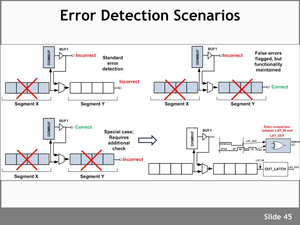
Error Detection Scenarios
Slide 45