Embed Size (px)
Citation preview
Quad ADC, Dual DAC, Low Latency, Low Power Codec
Data Sheet ADAU1372
FEATURES Low latency, 24-bit ADCs and DACs
102 dB SNR (through PGA and ADC with A-weighted filter) 107 dB dynamic range (through DAC and headphone with
A-weighted filter) Serial port sample rates from 8 kHz to 192 kHz 4 single-ended analog inputs, configurable as microphone or
line inputs Dual stereo digital microphone inputs Stereo analog audio output, single-ended or differential,
configurable as either line output or headphone driver PLL supporting any input clock rate from 8 MHz to 27 MHz Full-duplex, asynchronous sample rate converters (ASRCs) Power supplies
Analog and digital input/output of 1.8 V to 3.3 V Low power (15.5 mW) I2C and SPI control interfaces for flexibility 5 multipurpose pins supporting dual stereo digital
microphone inputs, mute, push-button volume controls
APPLICATIONS Handsets, headsets, and headphones Bluetooth® handsets, headsets, and headphones Personal navigation devices Digital still and video cameras
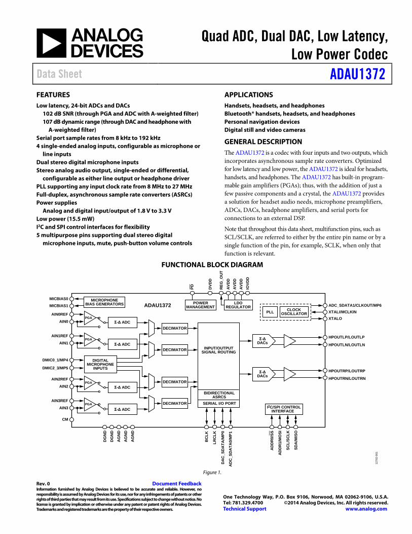
GENERAL DESCRIPTION The ADAU1372 is a codec with four inputs and two outputs, which incorporates asynchronous sample rate converters. Optimized for low latency and low power, the ADAU1372 is ideal for headsets, handsets, and headphones. The ADAU1372 has built-in program-mable gain amplifiers (PGAs); thus, with the addition of just a few passive components and a crystal, the ADAU1372 provides a solution for headset audio needs, microphone preamplifiers, ADCs, DACs, headphone amplifiers, and serial ports for connections to an external DSP.
Note that throughout this data sheet, multifunction pins, such as SCL/SCLK, are referred to either by the entire pin name or by a single function of the pin, for example, SCLK, when only that function is relevant.
FUNCTIONAL BLOCK DIAGRAM
Figure 1.
MICROPHONEBIAS GENERATORS
MICBIAS0
MICBIAS1
CM
DECIMATOR
AIN0REF
AIN0PGA
DECIMATOR
AIN1REF
AIN1PGA
AIN2REF
AIN2PGA
AIN3REF
AIN3PGA
DECIMATOR
DECIMATOR
DMIC0_1/MP4
DMIC2_3/MP5
DIGITALMICROPHONE
INPUTS
INPUT/OUTPUTSIGNAL ROUTING
I2C/SPI CONTROLINTERFACE
BIDIRECTIONALASRCS
SERIAL I/O PORT
LDOREGULATOR
REG
_OU
T
AVD
DA
VDD
AVD
DIO
VDD
DVD
D
POWERMANAGEMENT
PD
PLL CLOCKOSCILLATOR
DG
ND
DG
ND
AG
ND
AG
ND
AG
ND
AD
DR
0/SS
AD
DR
1/M
OSI
SCL/
SCLK
SDA
/MIS
O
DA
C_S
DA
TA/M
P0
ADC_SDATA1/CLKOUT/MP6XTALI/MCLKINXTALO
BC
LK
LRC
LK
ADAU1372
1270
2-00
1
HPOUTLP/LOUTLP
HPOUTLN/LOUTLN
HPOUTRP/LOUTRP
HPOUTRN/LOUTRN
AD
C_S
DA
TA0/
MP1
Σ-Δ ADC
Σ-Δ ADC
Σ-Δ ADC
Σ-Δ ADC
Σ-ΔDACs
Σ-ΔDACs
Rev. 0 Document Feedback Information furnished by Analog Devices is believed to be accurate and reliable. However, no responsibility is assumed by Analog Devices for its use, nor for any infringements of patents or other rights of third parties that may result from its use. Specifications subject to change without notice. No license is granted by implication or otherwise under any patent or patent rights of Analog Devices. Trademarks and registered trademarks are the property of their respective owners.
One Technology Way, P.O. Box 9106, Norwood, MA 02062-9106, U.S.A. Tel: 781.329.4700 ©2014 Analog Devices, Inc. All rights reserved. Technical Support www.analog.com
ADAU1372 Data Sheet
Rev. 0 | Page 2 of 92
TABLE OF CONTENTS Features .............................................................................................. 1
Applications ....................................................................................... 1
General Description ......................................................................... 1
Functional Block Diagram .............................................................. 1
Revision History ............................................................................... 3
Specifications ..................................................................................... 4
Analog Performance Specifications ........................................... 4
Crystal Amplifier Specifications ................................................. 7
Digital Input/Output Specifications........................................... 8
Power Supply Specifications........................................................ 8
Typical Power Consumption ....................................................... 9
Digital Filters ................................................................................. 9
Digital Timing Specifications ................................................... 10
Absolute Maximum Ratings .......................................................... 13
Thermal Resistance .................................................................... 13
ESD Caution ................................................................................ 13
Pin Configuration and Function Descriptions ........................... 14
Typical Performance Characteristics ........................................... 17
Theory of Operation ...................................................................... 24
System Clocking and Power-Up ................................................... 25
Initialization ................................................................................ 25
Clock Initialization ..................................................................... 25
PLL ............................................................................................... 25
Clock Output ............................................................................... 26
Power Sequencing ...................................................................... 26
Signal Routing ................................................................................. 27
Input Signal Paths ........................................................................... 28
Analog Inputs .............................................................................. 28
Digital Microphone Input ......................................................... 29
Analog-to-Digital Converters ................................................... 29
Output Signal Paths ........................................................................ 30
Analog Outputs........................................................................... 30
Digital-to-Analog Converters ................................................... 30
Asynchronous Sample Rate Converters .................................. 30
Control Port ..................................................................................... 31
Burst Mode Communication .................................................... 31
I2C Port ........................................................................................ 31
SPI Port ........................................................................................ 34
Burst Mode Communication .................................................... 34
Multipurpose Pins .......................................................................... 35
Push-Button Volume Controls ................................................. 35
Mute ............................................................................................. 35
Talkthrough Mode ..................................................................... 35
Serial Data Input/Output Ports .................................................... 36
Serial Port Initialization ............................................................ 36
Tristating Unused Channels...................................................... 37
Applications Information .............................................................. 39
Power Supply Bypass Capacitors .............................................. 39
Layout .......................................................................................... 39
Grounding ................................................................................... 39
Exposed Pad PCB Design ......................................................... 39
System Block Diagram ............................................................... 40
Register Summary: Low Latency Codec ..................................... 41
Register Details: Low Latency Codec .......................................... 43
Clock Control Register .............................................................. 43
PLL Denominator MSB Register .............................................. 44
PLL Denominator LSB Register ............................................... 44
PLL Numerator MSB Register .................................................. 44
PLL Numerator LSB Register .................................................... 44
PLL Integer Setting Register ..................................................... 45
PLL Lock Flag Register .............................................................. 46
CLKOUT Setting Selection Register ........................................ 46
Regulator Control Register ....................................................... 47
DAC Input Select Register ........................................................ 47
Serial Data Output 0/Serial Data Output 1 Input Select Register ........................................................................................ 48
Serial Data Output 2/Serial Data Output 3 Input Select Register ........................................................................................ 49
Serial Data Output 4/Serial Data Output 5 Input Select Register ........................................................................................ 50
Serial Data Output 6/Serial Data Output 7 Input Select Register ........................................................................................ 51
ADC_SDATA0/ADC_SDATA1 Channel Select Register ..... 53
Output ASRC0/Output ASRC1 Source Register .................... 53
Output ASRC2/Output ASRC3 Source Register .................... 54
Input ASRC Channel Select Register ....................................... 56
ADC Control 0 Register ............................................................ 56
ADC Control 1 Register ............................................................ 57
ADC Control 2 Register ............................................................ 58
ADC Control 3 Register ............................................................ 59
ADC0 Volume Control Register .............................................. 60
Data Sheet ADAU1372
Rev. 0 | Page 3 of 92
ADC1 Volume Control Register ............................................... 60
ADC2 Volume Control Register ............................................... 61
ADC3 Volume Control Register ............................................... 61
PGA Control 0 Register .............................................................. 62
PGA Control 1 Register .............................................................. 62
PGA Control 2 Register .............................................................. 63
PGA Control 3 Register .............................................................. 64
PGA Slew Control Register ........................................................ 64
PGA 10 dB Gain Boost Register ................................................ 65
Input and Output Capacitor Charging Register ..................... 66
ADC to DAC Talkthrough Bypass Path Register .................... 67
Talkthrough Bypass Gain for ADC0 Register ......................... 67
Talkthrough Bypass Gain for ADC1 Register ......................... 67
MICBIAS Control Register ........................................................ 68
DAC Control 1 Register ............................................................. 69
DAC0 Volume Control Register ................................................ 69
DAC1 Volume Control Register ................................................ 70
Headphone Output Mutes Register .......................................... 70
Serial Port Control 0 Register .................................................... 71
Serial Port Control 1 Register .................................................... 72
TDM Output Channel Disable Register .................................. 73
MP0 Function Setting Register ................................................. 74
MP1 Function Setting Register ................................................. 75
MP4 Function Setting Register ................................................. 76
MP5 Function Setting Register ................................................. 77
MP6 Function Setting Register ................................................. 78
Push-Button Volume Settings Register .................................... 79
Push-Button Volume Control Assignment Register .............. 80
Debounce Modes Register ......................................................... 81
Headphone Line Output Select Register .................................. 81
Decimator Power Control Register .......................................... 82
ASRC Interpolator and DAC Modulator Power Control Register ......................................................................................... 83
Analog Bias Control 0 Register ................................................. 84
Analog Bias Control 1 Register ................................................. 85
Digital Pin Pull-Up Control 0 Register .................................... 86
Digital Pin Pull-Up Control 1 Register .................................... 87
Digital Pin Pull-Down Control 2 Register .............................. 88
Digital Pin Pull-Down Control 3 Register .............................. 89
Digital Pin Drive Strength Control 4 Register ........................ 90
Digital Pin Drive Strength Control 5 Register ........................ 91
Outline Dimensions ........................................................................ 92
Ordering Guide ........................................................................... 92
REVISION HISTORY 12/14—Revision 0: Initial Version
ADAU1372 Data Sheet
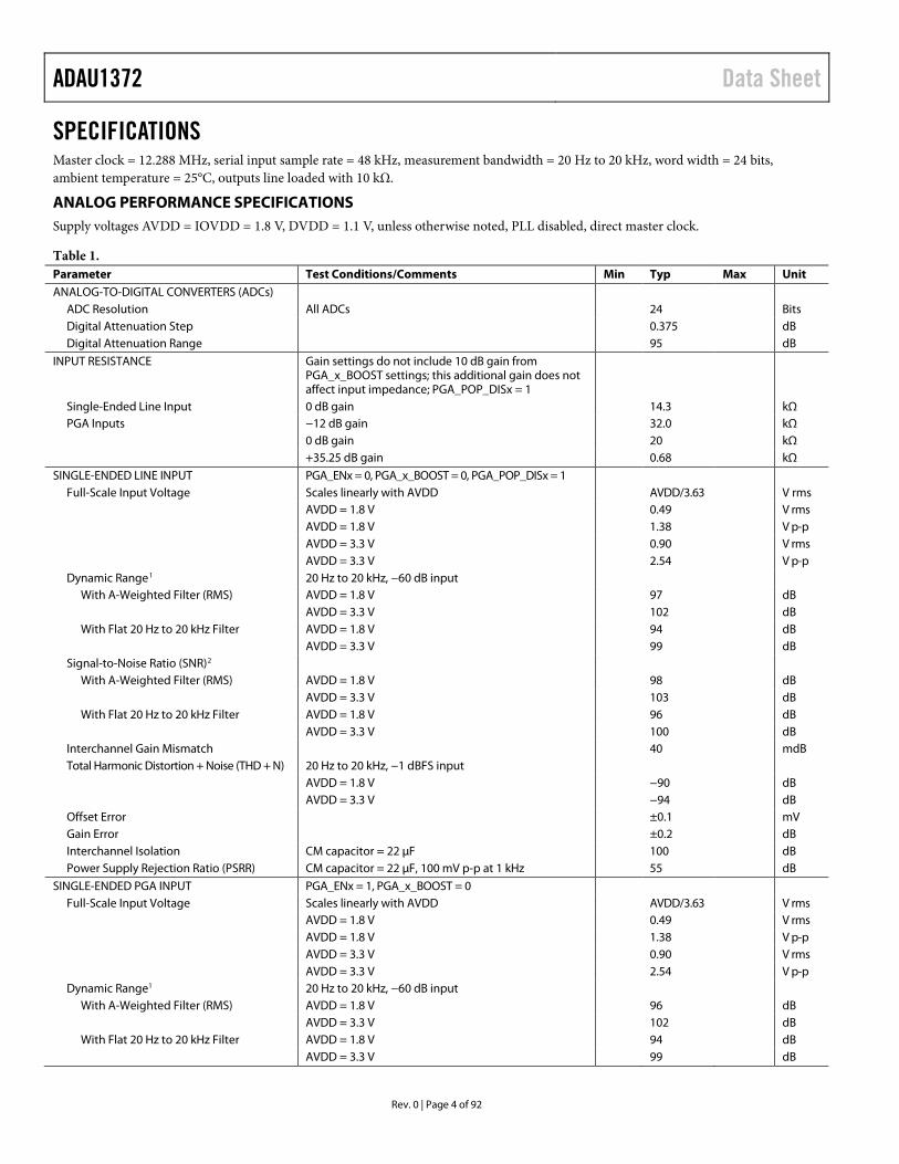
SPECIFICATIONS Master clock = 12.288 MHz, serial input sample rate = 48 kHz, measurement bandwidth = 20 Hz to 20 kHz, word width = 24 bits, ambient temperature = 25°C, outputs line loaded with 10 kΩ.
ANALOG PERFORMANCE SPECIFICATIONS Supply voltages AVDD = IOVDD = 1.8 V, DVDD = 1.1 V, unless otherwise noted, PLL disabled, direct master clock.
Table 1. Parameter Test Conditions/Comments Min Typ Max Unit ANALOG-TO-DIGITAL CONVERTERS (ADCs)
ADC Resolution All ADCs 24 Bits Digital Attenuation Step 0.375 dB Digital Attenuation Range 95 dB
INPUT RESISTANCE Gain settings do not include 10 dB gain from PGA_x_BOOST settings; this additional gain does not affect input impedance; PGA_POP_DISx = 1
Single-Ended Line Input 0 dB gain 14.3 kΩ PGA Inputs −12 dB gain 32.0 kΩ 0 dB gain 20 kΩ +35.25 dB gain 0.68 kΩ
SINGLE-ENDED LINE INPUT PGA_ENx = 0, PGA_x_BOOST = 0, PGA_POP_DISx = 1 Full-Scale Input Voltage Scales linearly with AVDD AVDD/3.63 V rms
AVDD = 1.8 V 0.49 V rms AVDD = 1.8 V 1.38 V p-p AVDD = 3.3 V 0.90 V rms AVDD = 3.3 V 2.54 V p-p
Dynamic Range1 20 Hz to 20 kHz, −60 dB input With A-Weighted Filter (RMS) AVDD = 1.8 V 97 dB AVDD = 3.3 V 102 dB With Flat 20 Hz to 20 kHz Filter AVDD = 1.8 V 94 dB AVDD = 3.3 V 99 dB
Signal-to-Noise Ratio (SNR)2 With A-Weighted Filter (RMS) AVDD = 1.8 V 98 dB AVDD = 3.3 V 103 dB With Flat 20 Hz to 20 kHz Filter AVDD = 1.8 V 96 dB AVDD = 3.3 V 100 dB
Interchannel Gain Mismatch 40 mdB Total Harmonic Distortion + Noise (THD + N) 20 Hz to 20 kHz, −1 dBFS input AVDD = 1.8 V −90 dB AVDD = 3.3 V −94 dB Offset Error ±0.1 mV Gain Error ±0.2 dB Interchannel Isolation CM capacitor = 22 µF 100 dB Power Supply Rejection Ratio (PSRR) CM capacitor = 22 µF, 100 mV p-p at 1 kHz 55 dB
SINGLE-ENDED PGA INPUT PGA_ENx = 1, PGA_x_BOOST = 0 Full-Scale Input Voltage Scales linearly with AVDD AVDD/3.63 V rms AVDD = 1.8 V 0.49 V rms AVDD = 1.8 V 1.38 V p-p AVDD = 3.3 V 0.90 V rms AVDD = 3.3 V 2.54 V p-p Dynamic Range1 20 Hz to 20 kHz, −60 dB input
With A-Weighted Filter (RMS) AVDD = 1.8 V 96 dB AVDD = 3.3 V 102 dB With Flat 20 Hz to 20 kHz Filter AVDD = 1.8 V 94 dB AVDD = 3.3 V 99 dB
Rev. 0 | Page 4 of 92
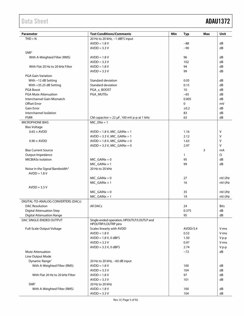
Data Sheet ADAU1372 Parameter Test Conditions/Comments Min Typ Max Unit
THD + N 20 Hz to 20 kHz, −1 dBFS input AVDD = 1.8 V −88 dB AVDD = 3.3 V −90 dB
SNR2 With A-Weighted Filter (RMS) AVDD = 1.8 V 96 dB AVDD = 3.3 V 102 dB With Flat 20 Hz to 20 kHz Filter AVDD = 1.8 V 94 dB AVDD = 3.3 V 99 dB
PGA Gain Variation With −12 dB Setting Standard deviation 0.05 dB With +35.25 dB Setting Standard deviation 0.15 dB
PGA Boost PGA_x_BOOST 10 dB PGA Mute Attenuation PGA_MUTEx −65 dB Interchannel Gain Mismatch 0.005 dB Offset Error 0 mV Gain Error ±0.2 dB Interchannel Isolation 83 dB PSRR CM capacitor = 22 µF, 100 mV p-p at 1 kHz 63 dB
MICROPHONE BIAS MIC_ENx = 1 Bias Voltage
0.65 × AVDD AVDD = 1.8 V, MIC_GAINx = 1 1.16 V AVDD = 3.3 V, MIC_GAINx = 1 2.12 V
0.90 × AVDD AVDD = 1.8 V, MIC_GAINx = 0 1.63 V AVDD = 3.3 V, MIC_GAINx = 0 2.97 V Bias Current Source 3 mA Output Impedance 1 Ω MICBIASx Isolation MIC_GAINx = 0 95 dB MIC_GAINx = 1 99 dB Noise in the Signal Bandwidth3 20 Hz to 20 kHz
AVDD = 1.8 V MIC_GAINx = 0 27 nV/√Hz MIC_GAINx = 1 16 nV/√Hz AVDD = 3.3 V MIC_GAINx = 0 35 nV/√Hz MIC_GAINx = 1 19 nV/√Hz
DIGITAL-TO-ANALOG CONVERTERS (DACs) DAC Resolution All DACs 24 Bits Digital Attenuation Step 0.375 dB Digital Attenuation Range 95 dB
DAC SINGLE-ENDED OUTPUT Single-ended operation, HPOUTLP/LOUTLP and HPOUTRP/LOUTRP pins
Full-Scale Output Voltage Scales linearly with AVDD AVDD/3.4 V rms AVDD = 1.8 V 0.53 V rms AVDD = 1.8 V, 0 dBFS 1.50 V p-p AVDD = 3.3 V 0.97 V rms AVDD = 3.3 V, 0 dBFS 2.74 V p-p Mute Attenuation −72 dB Line Output Mode
Dynamic Range1 20 Hz to 20 kHz, −60 dB input With A-Weighted Filter (RMS) AVDD = 1.8 V 100 dB AVDD = 3.3 V 104 dB With Flat 20 Hz to 20 kHz Filter AVDD = 1.8 V 97 dB AVDD = 3.3 V 101 dB
SNR2 20 Hz to 20 kHz With A-Weighted Filter (RMS) AVDD = 1.8 V 100 dB AVDD = 3.3 V 104 dB
Rev. 0 | Page 5 of 92
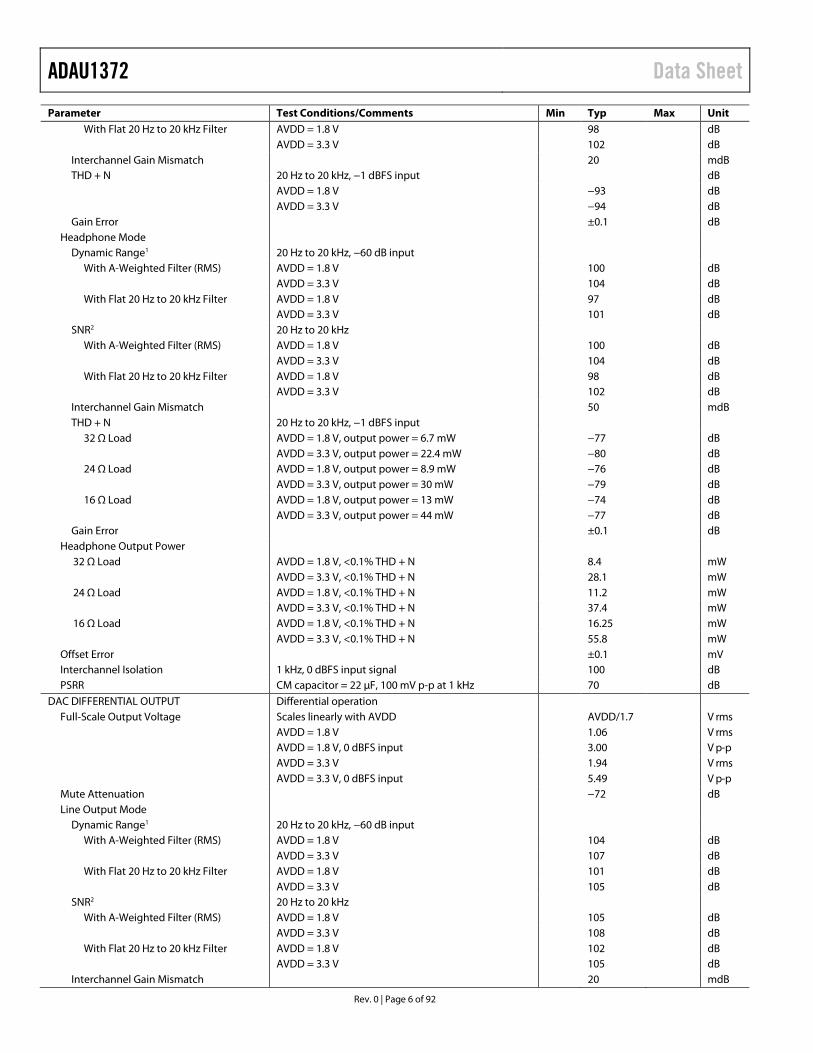
ADAU1372 Data Sheet Parameter Test Conditions/Comments Min Typ Max Unit
With Flat 20 Hz to 20 kHz Filter AVDD = 1.8 V 98 dB AVDD = 3.3 V 102 dB
Interchannel Gain Mismatch 20 mdB THD + N 20 Hz to 20 kHz, −1 dBFS input dB AVDD = 1.8 V −93 dB AVDD = 3.3 V −94 dB Gain Error ±0.1 dB
Headphone Mode Dynamic Range1 20 Hz to 20 kHz, −60 dB input
With A-Weighted Filter (RMS) AVDD = 1.8 V 100 dB AVDD = 3.3 V 104 dB With Flat 20 Hz to 20 kHz Filter AVDD = 1.8 V 97 dB AVDD = 3.3 V 101 dB
SNR2 20 Hz to 20 kHz With A-Weighted Filter (RMS) AVDD = 1.8 V 100 dB AVDD = 3.3 V 104 dB With Flat 20 Hz to 20 kHz Filter AVDD = 1.8 V 98 dB AVDD = 3.3 V 102 dB
Interchannel Gain Mismatch 50 mdB THD + N 20 Hz to 20 kHz, −1 dBFS input
32 Ω Load AVDD = 1.8 V, output power = 6.7 mW −77 dB AVDD = 3.3 V, output power = 22.4 mW −80 dB 24 Ω Load AVDD = 1.8 V, output power = 8.9 mW −76 dB
AVDD = 3.3 V, output power = 30 mW −79 dB 16 Ω Load AVDD = 1.8 V, output power = 13 mW −74 dB
AVDD = 3.3 V, output power = 44 mW −77 dB Gain Error ±0.1 dB
Headphone Output Power 32 Ω Load AVDD = 1.8 V, <0.1% THD + N 8.4 mW AVDD = 3.3 V, <0.1% THD + N 28.1 mW 24 Ω Load AVDD = 1.8 V, <0.1% THD + N 11.2 mW AVDD = 3.3 V, <0.1% THD + N 37.4 mW 16 Ω Load AVDD = 1.8 V, <0.1% THD + N 16.25 mW AVDD = 3.3 V, <0.1% THD + N 55.8 mW
Offset Error ±0.1 mV Interchannel Isolation 1 kHz, 0 dBFS input signal 100 dB PSRR CM capacitor = 22 µF, 100 mV p-p at 1 kHz 70 dB
DAC DIFFERENTIAL OUTPUT Differential operation Full-Scale Output Voltage Scales linearly with AVDD AVDD/1.7 V rms AVDD = 1.8 V 1.06 V rms AVDD = 1.8 V, 0 dBFS input 3.00 V p-p AVDD = 3.3 V 1.94 V rms AVDD = 3.3 V, 0 dBFS input 5.49 V p-p Mute Attenuation −72 dB Line Output Mode
Dynamic Range1 20 Hz to 20 kHz, −60 dB input With A-Weighted Filter (RMS) AVDD = 1.8 V 104 dB AVDD = 3.3 V 107 dB With Flat 20 Hz to 20 kHz Filter AVDD = 1.8 V 101 dB AVDD = 3.3 V 105 dB
SNR2 20 Hz to 20 kHz With A-Weighted Filter (RMS) AVDD = 1.8 V 105 dB AVDD = 3.3 V 108 dB With Flat 20 Hz to 20 kHz Filter AVDD = 1.8 V 102 dB AVDD = 3.3 V 105 dB
Interchannel Gain Mismatch 20 mdB
Rev. 0 | Page 6 of 92
Data Sheet ADAU1372 Parameter Test Conditions/Comments Min Typ Max Unit
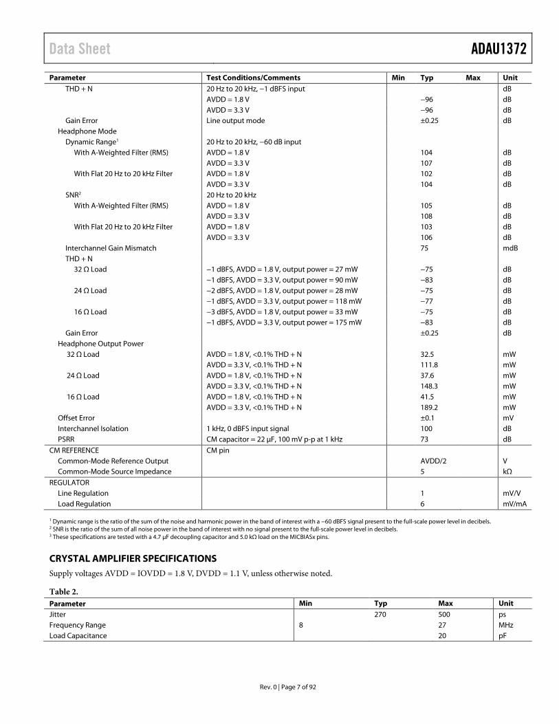
THD + N 20 Hz to 20 kHz, −1 dBFS input dB AVDD = 1.8 V −96 dB AVDD = 3.3 V −96 dB Gain Error Line output mode ±0.25 dB
Headphone Mode Dynamic Range1 20 Hz to 20 kHz, −60 dB input
With A-Weighted Filter (RMS) AVDD = 1.8 V 104 dB AVDD = 3.3 V 107 dB With Flat 20 Hz to 20 kHz Filter AVDD = 1.8 V 102 dB AVDD = 3.3 V 104 dB
SNR2 20 Hz to 20 kHz With A-Weighted Filter (RMS) AVDD = 1.8 V 105 dB AVDD = 3.3 V 108 dB With Flat 20 Hz to 20 kHz Filter AVDD = 1.8 V 103 dB AVDD = 3.3 V 106 dB
Interchannel Gain Mismatch 75 mdB THD + N
32 Ω Load −1 dBFS, AVDD = 1.8 V, output power = 27 mW −75 dB −1 dBFS, AVDD = 3.3 V, output power = 90 mW −83 dB 24 Ω Load −2 dBFS, AVDD = 1.8 V, output power = 28 mW −75 dB
−1 dBFS, AVDD = 3.3 V, output power = 118 mW −77 dB 16 Ω Load −3 dBFS, AVDD = 1.8 V, output power = 33 mW −75 dB
−1 dBFS, AVDD = 3.3 V, output power = 175 mW −83 dB Gain Error ±0.25 dB
Headphone Output Power 32 Ω Load AVDD = 1.8 V, <0.1% THD + N 32.5 mW AVDD = 3.3 V, <0.1% THD + N 111.8 mW 24 Ω Load AVDD = 1.8 V, <0.1% THD + N 37.6 mW AVDD = 3.3 V, <0.1% THD + N 148.3 mW 16 Ω Load AVDD = 1.8 V, <0.1% THD + N 41.5 mW AVDD = 3.3 V, <0.1% THD + N 189.2 mW
Offset Error ±0.1 mV Interchannel Isolation 1 kHz, 0 dBFS input signal 100 dB PSRR CM capacitor = 22 µF, 100 mV p-p at 1 kHz 73 dB
CM REFERENCE CM pin Common-Mode Reference Output AVDD/2 V Common-Mode Source Impedance 5 kΩ
REGULATOR Line Regulation 1 mV/V Load Regulation 6 mV/mA
1 Dynamic range is the ratio of the sum of the noise and harmonic power in the band of interest with a −60 dBFS signal present to the full-scale power level in decibels. 2 SNR is the ratio of the sum of all noise power in the band of interest with no signal present to the full-scale power level in decibels. 3 These specifications are tested with a 4.7 µF decoupling capacitor and 5.0 kΩ load on the MICBIASx pins.
CRYSTAL AMPLIFIER SPECIFICATIONS Supply voltages AVDD = IOVDD = 1.8 V, DVDD = 1.1 V, unless otherwise noted.
Table 2. Parameter Min Typ Max Unit Jitter 270 500 ps Frequency Range 8 27 MHz Load Capacitance 20 pF
Rev. 0 | Page 7 of 92
ADAU1372 Data Sheet
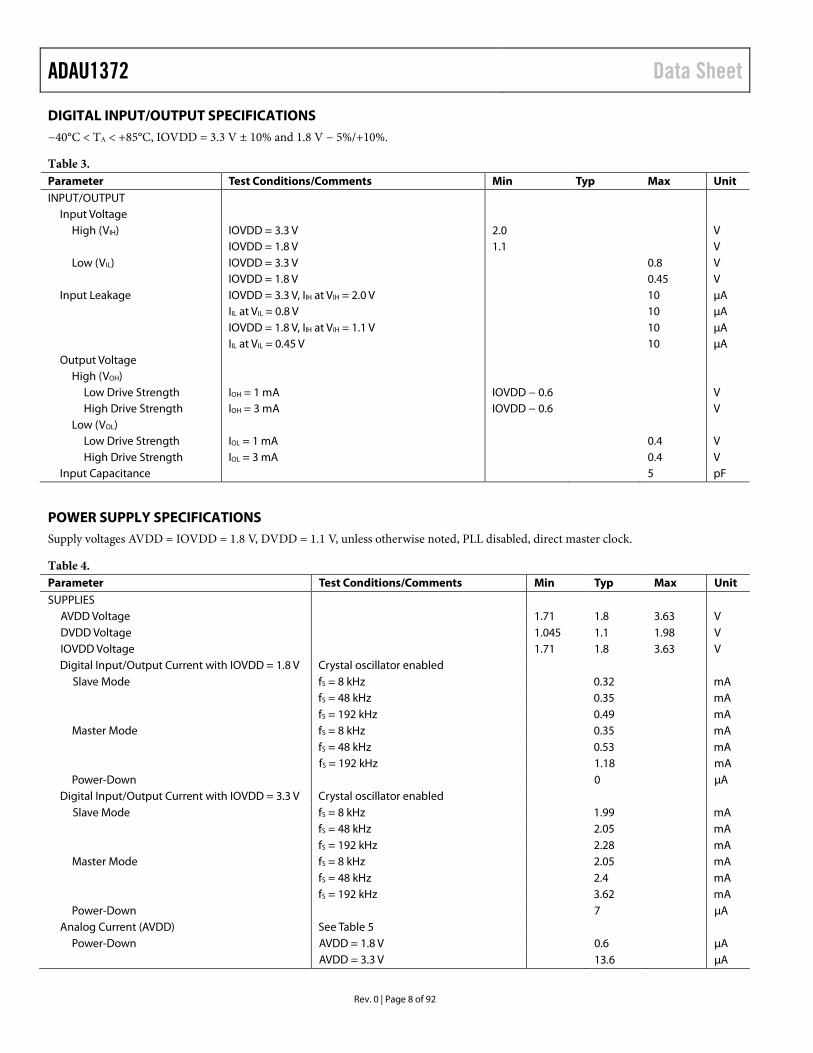
DIGITAL INPUT/OUTPUT SPECIFICATIONS −40°C < TA < +85°C, IOVDD = 3.3 V ± 10% and 1.8 V − 5%/+10%.
Table 3. Parameter Test Conditions/Comments Min Typ Max Unit INPUT/OUTPUT
Input Voltage High (VIH) IOVDD = 3.3 V 2.0 V IOVDD = 1.8 V 1.1 V Low (VIL) IOVDD = 3.3 V 0.8 V IOVDD = 1.8 V 0.45 V
Input Leakage IOVDD = 3.3 V, IIH at VIH = 2.0 V 10 µA IIL at VIL = 0.8 V 10 µA IOVDD = 1.8 V, IIH at VIH = 1.1 V 10 µA IIL at VIL = 0.45 V 10 µA Output Voltage
High (VOH) Low Drive Strength IOH = 1 mA IOVDD − 0.6 V High Drive Strength IOH = 3 mA IOVDD − 0.6 V
Low (VOL) Low Drive Strength IOL = 1 mA 0.4 V High Drive Strength IOL = 3 mA 0.4 V
Input Capacitance 5 pF
POWER SUPPLY SPECIFICATIONS Supply voltages AVDD = IOVDD = 1.8 V, DVDD = 1.1 V, unless otherwise noted, PLL disabled, direct master clock.
Table 4. Parameter Test Conditions/Comments Min Typ Max Unit SUPPLIES
AVDD Voltage 1.71 1.8 3.63 V DVDD Voltage 1.045 1.1 1.98 V IOVDD Voltage 1.71 1.8 3.63 V Digital Input/Output Current with IOVDD = 1.8 V Crystal oscillator enabled
Slave Mode fS = 8 kHz 0.32 mA fS = 48 kHz 0.35 mA
fS = 192 kHz 0.49 mA Master Mode fS = 8 kHz 0.35 mA fS = 48 kHz 0.53 mA fS = 192 kHz 1.18 mA Power-Down 0 µA
Digital Input/Output Current with IOVDD = 3.3 V Crystal oscillator enabled Slave Mode fS = 8 kHz 1.99 mA fS = 48 kHz 2.05 mA
fS = 192 kHz 2.28 mA Master Mode fS = 8 kHz 2.05 mA fS = 48 kHz 2.4 mA
fS = 192 kHz 3.62 mA Power-Down 7 µA
Analog Current (AVDD) See Table 5 Power-Down AVDD = 1.8 V 0.6 µA AVDD = 3.3 V 13.6 µA
Rev. 0 | Page 8 of 92
Data Sheet ADAU1372
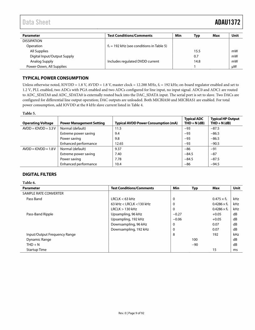
Parameter Test Conditions/Comments Min Typ Max Unit DISSIPATION
Operation fS = 192 kHz (see conditions in Table 5) All Supplies 15.5 mW Digital Input/Output Supply 0.7 mW Analog Supply Includes regulated DVDD current 14.8 mW
Power-Down, All Supplies 1 µW
TYPICAL POWER CONSUMPTION Unless otherwise noted, IOVDD = 1.8 V, AVDD = 1.8 V, master clock = 12.288 MHz, fS = 192 kHz; on-board regulator enabled and set to 1.2 V, PLL enabled, two ADCs with PGA enabled and two ADCs configured for line input, no input signal. ADC0 and ADC1 are routed to ADC_SDATA0 and ADC_SDATA0 is externally routed back into the DAC_SDATA input. The serial port is set to slave. Two DACs are configured for differential line output operation; DAC outputs are unloaded. Both MICBIAS0 and MICBIAS1 are enabled. For total power consumption, add IOVDD at the 8 kHz slave current listed in Table 4.
Table 5.
Operating Voltage Power Management Setting Typical AVDD Power Consumption (mA) Typical ADC THD + N (dB)
Typical HP Output THD + N (dB)
AVDD = IOVDD = 3.3 V Normal (default) 11.5 −93 −87.5 Extreme power saving 9.4 −93 −86.5 Power saving 9.8 −93 −86.5 Enhanced performance 12.65 −93 −90.5 AVDD = IOVDD = 1.8 V Normal (default) 9.37 −86 −91 Extreme power saving 7.40 −84.5 −87 Power saving 7.78 −84.5 −87.5 Enhanced performance 10.4 −86 −94.5
DIGITAL FILTERS
Table 6. Parameter Test Conditions/Comments Min Typ Max Unit SAMPLE RATE CONVERTER
Pass Band LRCLK < 63 kHz 0 0.475 × fS kHz 63 kHz < LRCLK <130 kHz 0 0.4286 × fS kHz LRCLK > 130 kHz 0 0.4286 × fS kHz Pass-Band Ripple Upsampling, 96 kHz −0.27 +0.05 dB Upsampling, 192 kHz −0.06 +0.05 dB Downsampling, 96 kHz 0 0.07 dB Downsampling, 192 kHz 0 0.07 dB Input/Output Frequency Range 8 192 kHz Dynamic Range 100 dB THD + N −90 dB Startup Time 15 ms
Rev. 0 | Page 9 of 92
ADAU1372 Data Sheet
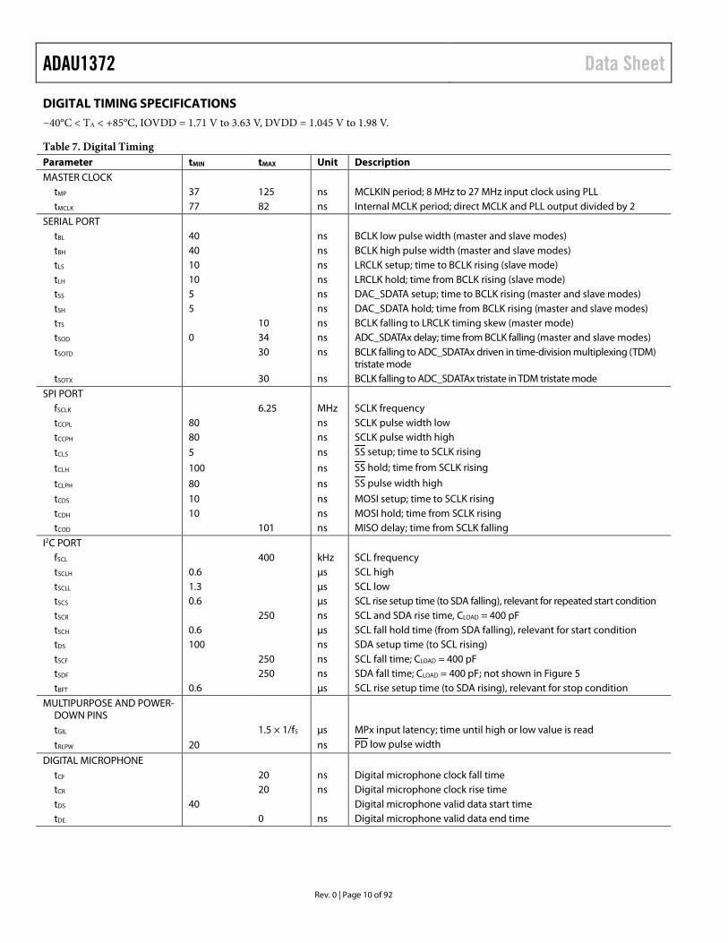
DIGITAL TIMING SPECIFICATIONS −40°C < TA < +85°C, IOVDD = 1.71 V to 3.63 V, DVDD = 1.045 V to 1.98 V.
Table 7. Digital Timing Parameter tMIN tMAX Unit Description MASTER CLOCK
tMP 37 125 ns MCLKIN period; 8 MHz to 27 MHz input clock using PLL tMCLK 77 82 ns Internal MCLK period; direct MCLK and PLL output divided by 2
SERIAL PORT tBL 40 ns BCLK low pulse width (master and slave modes) tBH 40 ns BCLK high pulse width (master and slave modes) tLS 10 ns LRCLK setup; time to BCLK rising (slave mode) tLH 10 ns LRCLK hold; time from BCLK rising (slave mode) tSS 5 ns DAC_SDATA setup; time to BCLK rising (master and slave modes) tSH 5 ns DAC_SDATA hold; time from BCLK rising (master and slave modes) tTS 10 ns BCLK falling to LRCLK timing skew (master mode) tSOD 0 34 ns ADC_SDATAx delay; time from BCLK falling (master and slave modes) tSOTD 30 ns BCLK falling to ADC_SDATAx driven in time-division multiplexing (TDM)
tristate mode tSOTX 30 ns BCLK falling to ADC_SDATAx tristate in TDM tristate mode
SPI PORT fSCLK 6.25 MHz SCLK frequency tCCPL 80 ns SCLK pulse width low tCCPH 80 ns SCLK pulse width high tCLS 5 ns SS setup; time to SCLK rising
tCLH 100 ns SS hold; time from SCLK rising
tCLPH 80 ns SS pulse width high
tCDS 10 ns MOSI setup; time to SCLK rising tCDH 10 ns MOSI hold; time from SCLK rising tCOD 101 ns MISO delay; time from SCLK falling
I2C PORT fSCL 400 kHz SCL frequency tSCLH 0.6 µs SCL high tSCLL 1.3 µs SCL low tSCS 0.6 µs SCL rise setup time (to SDA falling), relevant for repeated start condition tSCR 250 ns SCL and SDA rise time, CLOAD = 400 pF tSCH 0.6 µs SCL fall hold time (from SDA falling), relevant for start condition tDS 100 ns SDA setup time (to SCL rising) tSCF 250 ns SCL fall time; CLOAD = 400 pF tSDF 250 ns SDA fall time; CLOAD = 400 pF; not shown in Figure 5 tBFT 0.6 µs SCL rise setup time (to SDA rising), relevant for stop condition
MULTIPURPOSE AND POWER-DOWN PINS
tGIL 1.5 × 1/fS µs MPx input latency; time until high or low value is read tRLPW 20 ns PD low pulse width
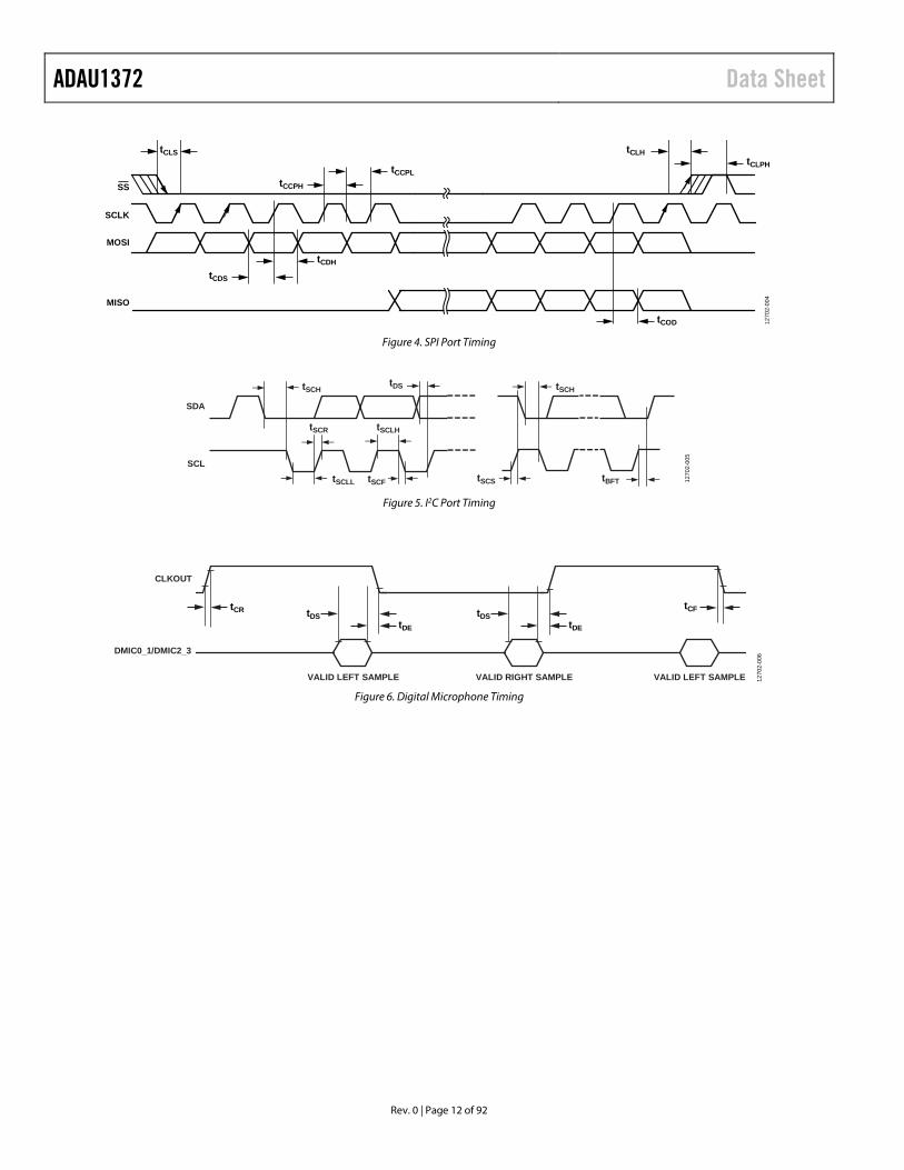
DIGITAL MICROPHONE tCF 20 ns Digital microphone clock fall time tCR 20 ns Digital microphone clock rise time tDS 40 Digital microphone valid data start time tDE 0 ns Digital microphone valid data end time
Rev. 0 | Page 10 of 92
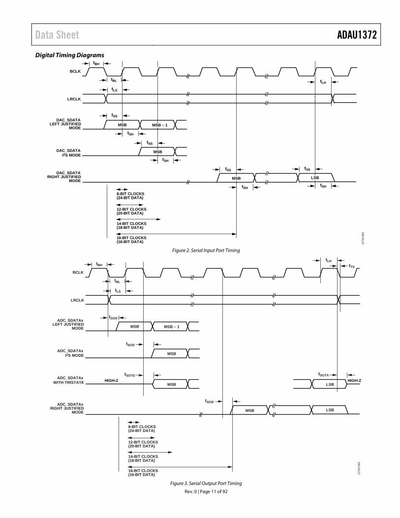
Data Sheet ADAU1372 Digital Timing Diagrams
Figure 2. Serial Input Port Timing
Figure 3. Serial Output Port Timing
BCLK
LRCLK
DAC_SDATALEFT JUSTIFIED
MODE
LSB
DAC_SDATAI2S MODE
DAC_SDATARIGHT JUSTIFIED
MODE
tBH
MSB MSB – 1
MSB
MSB
8-BIT CLOCKS(24-BIT DATA)
12-BIT CLOCKS(20-BIT DATA)
14-BIT CLOCKS(18-BIT DATA)
16-BIT CLOCKS(16-BIT DATA)
tLS
tSS
tSH
tSH
tSS
tSS
tSH
tSS
tSH
tLHtBL
1270
2-00
2
LRCLK
LSB
ADC_SDATAxI2S MODE
ADC_SDATAxRIGHT JUSTIFIED
MODE
MSB
ADC_SDATAxLEFT JUSTIFIED
MODE MSB MSB – 1
ADC_SDATAx WITH TRISTATE MSB LSB
MSB
8-BIT CLOCKS(24-BIT DATA)
12-BIT CLOCKS(20-BIT DATA)
14-BIT CLOCKS(18-BIT DATA)
16-BIT CLOCKS(16-BIT DATA)
tLS
tSOD
tSOD
tSOTD
tSOD
tSOTX
tLHtTS
tBL
BCLK
tBH
HIGH-Z HIGH-Z
1270
2-00
3
Rev. 0 | Page 11 of 92
ADAU1372 Data Sheet
Figure 4. SPI Port Timing
Figure 5. I2C Port Timing
Figure 6. Digital Microphone Timing
SS
SCLK
MOSI
MISO
tCLS
tCDS
tCDH
tCOD
tCCPH
tCCPL
tCLHtCLPH
1270
2-00
4
tSCH
tSCLHtSCR
tSCLL tSCF
tDS
SDA
SCL
tSCH
tBFTtSCS 1270
2-00
5
DMIC0_1/DMIC2_3
VALID LEFT SAMPLE VALID LEFT SAMPLEVALID RIGHT SAMPLE
CLKOUT
tCR tCFtDStDE
tDStDE
1270
2-00
6
Rev. 0 | Page 12 of 92
Data Sheet ADAU1372
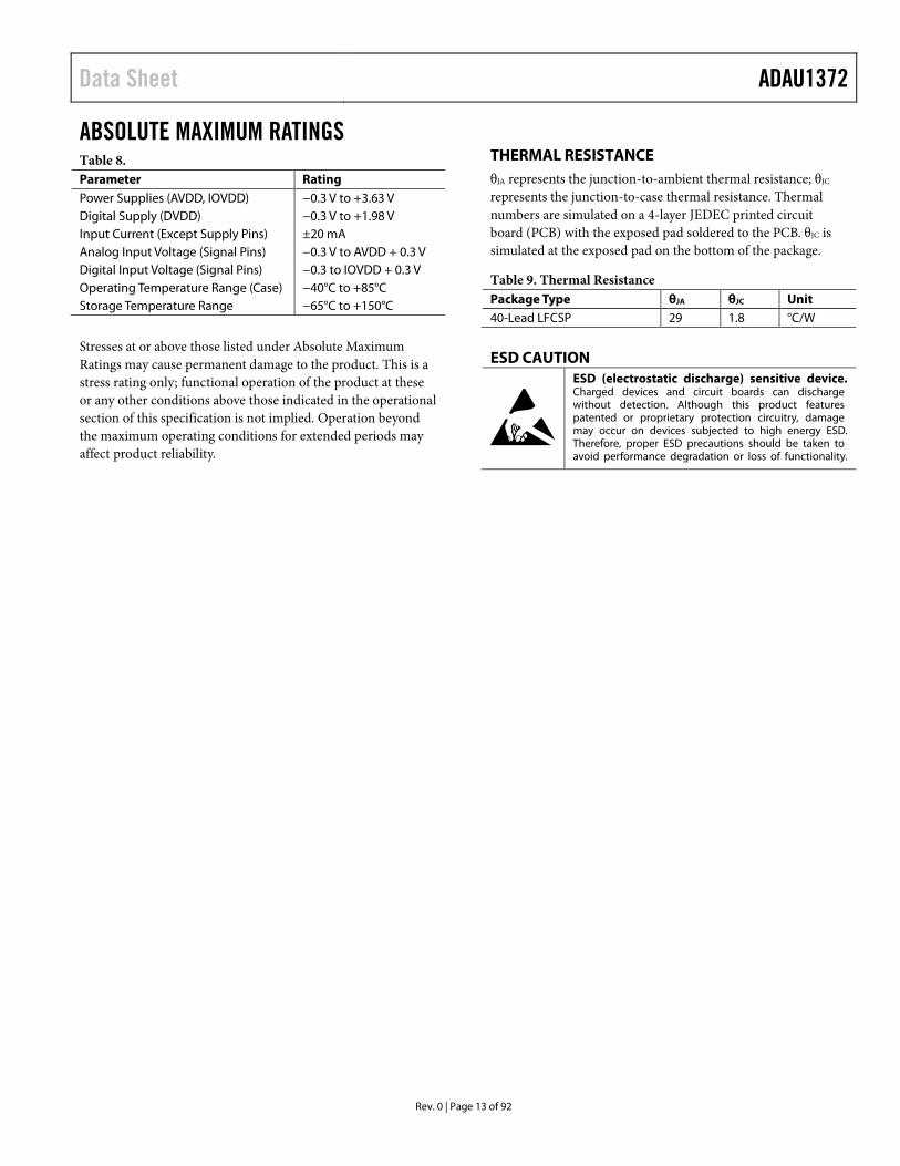
ABSOLUTE MAXIMUM RATINGS Table 8. Parameter Rating Power Supplies (AVDD, IOVDD) −0.3 V to +3.63 V Digital Supply (DVDD) −0.3 V to +1.98 V Input Current (Except Supply Pins) ±20 mA Analog Input Voltage (Signal Pins) −0.3 V to AVDD + 0.3 V Digital Input Voltage (Signal Pins) −0.3 to IOVDD + 0.3 V Operating Temperature Range (Case) −40°C to +85°C Storage Temperature Range −65°C to +150°C
Stresses at or above those listed under Absolute Maximum Ratings may cause permanent damage to the product. This is a stress rating only; functional operation of the product at these or any other conditions above those indicated in the operational section of this specification is not implied. Operation beyond the maximum operating conditions for extended periods may affect product reliability.
THERMAL RESISTANCE θJA represents the junction-to-ambient thermal resistance; θJC
represents the junction-to-case thermal resistance. Thermal numbers are simulated on a 4-layer JEDEC printed circuit board (PCB) with the exposed pad soldered to the PCB. θJC is simulated at the exposed pad on the bottom of the package.
Table 9. Thermal Resistance Package Type θJA θJC Unit 40-Lead LFCSP 29 1.8 °C/W
ESD CAUTION
Rev. 0 | Page 13 of 92
ADAU1372 Data Sheet
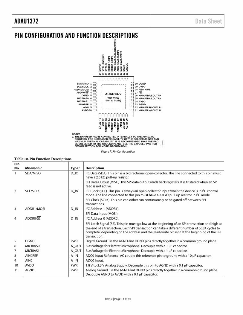
PIN CONFIGURATION AND FUNCTION DESCRIPTIONS
Figure 7. Pin Configuration
Table 10. Pin Function Descriptions Pin No. Mnemonic Type1 Description 1 SDA/MISO D_IO I2C Data (SDA). This pin is a bidirectional open-collector. The line connected to this pin must
have a 2.0 kΩ pull-up resistor. SPI Data Output (MISO). This SPI data output reads back registers. It is tristated when an SPI
read is not active. 2 SCL/SCLK D_IN I2C Clock (SCL). This pin is always an open-collector input when the device is in I2C control
mode. The line connected to this pin must have a 2.0 kΩ pull-up resistor in I2C mode. SPI Clock (SCLK). This pin can either run continuously or be gated off between SPI
transactions. 3 ADDR1/MOSI D_IN I2C Address 1 (ADDR1). SPI Data Input (MOSI). 4 ADDR0/SS D_IN I2C Address 0 (ADDR0).
SPI Latch Signal (SS). This pin must go low at the beginning of an SPI transaction and high at the end of a transaction. Each SPI transaction can take a different number of SCLK cycles to complete, depending on the address and the read/write bit sent at the beginning of the SPI transaction.
5 DGND PWR Digital Ground. Tie the AGND and DGND pins directly together in a common ground plane. 6 MICBIAS0 A_OUT Bias Voltage for Electret Microphone. Decouple with a 1 µF capacitor. 7 MICBIAS1 A_OUT Bias Voltage for Electret Microphone. Decouple with a 1 µF capacitor. 8 AIN0REF A_IN ADC0 Input Reference. AC couple this reference pin to ground with a 10 µF capacitor. 9 AIN0 A_IN ADC0 Input. 10 AVDD PWR 1.8 V to 3.3 V Analog Supply. Decouple this pin to AGND with a 0.1 µF capacitor. 11 AGND PWR Analog Ground. Tie the AGND and DGND pins directly together in a common ground plane.
Decouple AGND to AVDD with a 0.1 µF capacitor.
1SDA/MISO2SCL/SCLK3ADDR1/MOSI4ADDR0/SS5DGND6MICBIAS07MICBIAS18AIN0REF9AIN0
10AVDD
23 AGND24 AVDD25 HPOUTRN/LOUTRN26 HPOUTRP/LOUTRP27 PD28 REG_OUT29 DVDD30 DGND
22 HPOUTLP/LOUTLP21 HPOUTLN/LOUTLN
11A
GN
D12
CM
13A
IN1R
EF
15A
IN2R
EF
17A
IN3R
EF16
AIN
2
18A
IN3
19A
VDD
20A
GN
D
14A
IN1
33D
AC
_SD
ATA
/MP0
34A
DC
_SD
ATA
0/M
P135
AD
C_S
DA
TA1/
CLK
OU
T/M
P636
DM
IC2_
3/M
P537
DM
IC0_
1/M
P438
XTA
LO39
XTA
LI/M
CLK
IN40
IOVD
D
32B
CLK
31LR
CLK
TOP VIEW(Not to Scale)
ADAU1372
NOTES1. THE EXPOSED PAD IS CONNECTED INTERNALLY TO THE ADAU1372
GROUNDS. FOR INCREASED RELIABILITY OF THE SOLDER JOINTS ANDMAXIMUM THERMAL CAPABILITY, IT IS RECOMMENDED THAT THE PADBE SOLDERED TO THE GROUND PLANE. SEE THE EXPOSED PAD PCBDESIGN SECTION FOR MORE INFORMATION. 12
702-
007
Rev. 0 | Page 14 of 92
Data Sheet ADAU1372
Pin No. Mnemonic Type1 Description 12 CM A_OUT AVDD/2 V Common-Mode Reference. Connect a 10 µF to 47 µF decoupling capacitor
between this pin and ground to reduce crosstalk between the ADCs and DACs. The material of the capacitors is not critical. This pin can be used to bias external analog circuits, as long as they are not drawing current from CM (for example, the noninverting input of an operational amplifier).
13 AIN1REF A_IN ADC1 Input Reference. AC couple this reference pin to ground with a 10 µF capacitor. 14 AIN1 A_IN ADC1 Input. 15 AIN2REF A_IN ADC2 Input Reference. AC couple this reference pin to ground with a 10 µF capacitor. 16 AIN2 A_IN ADC2 Input. 17 AIN3REF A_IN ADC3 Input Reference. AC couple this reference pin to ground with a 10 µF capacitor. 18 AIN3 A_IN ADC3 Input. 19 AVDD PWR 1.8 V to 3.3 V Analog Supply. Decouple this pin to AGND with a 0.1 µF capacitor. 20 AGND PWR Analog Ground. See the Grounding section. 21 HPOUTLN/LOUTLN A_OUT Left Headphone Inverted (HPOUTLN). Line Output Inverted (LOUTLN). 22 HPOUTLP/LOUTLP A_OUT Left Headphone Noninverted (HPOUTLP). Line Output Noninverted, Single-Ended Line Output (LOUTLP). 23 AGND PWR Headphone Amplifier Ground. See the Grounding section. 24 AVDD PWR Headphone Amplifier Power, 1.8 V to 3.3 V Analog Supply. Decouple this pin to AGND with a
0.1 µF capacitor. The PCB trace to this pin must be able to supply the higher current necessary for driving the headphone outputs.
25 HPOUTRN/LOUTRN A_OUT Right Headphone Inverted (HPOUTRN). Line Output Inverted (LOUTRN). 26 HPOUTRP/LOUTRP A_OUT Right Headphone Noninverted (HPOUTRP). Line Output Noninverted, Single-Ended Line Output (LOUTRP). 27 PD D_IN Active Low Power-Down. All digital and analog circuits are powered down. There is an
internal pull-down resistor on this pin; therefore, the ADAU1372 is held in power-down mode if its input signal is floating while power is applied to the supply pins.
28 REG_OUT A_OUT Regulator Output Voltage. Connect this pin to DVDD if the internal voltage regulator is generating the DVDD voltage.
29 DVDD PWR Digital Core Supply. The digital supply can be generated from an on-board regulator or supplied directly from an external supply. In each case, decouple DVDD to DGND with a 0.1 µF capacitor.
30 DGND PWR Digital Ground. See the Grounding section. 31 LRCLK D_IO Serial Data Port Frame Clock. 32 BCLK D_IO Serial Data Port Bit Clock. 33 DAC_SDATA/MP0 D_IO DAC Serial Input Data (DAC_SDATA). General-Purpose Input (MP0). 34 ADC_SDATA0/MP1 D_IO ADC Serial Data Output 0 (ADC_SDATA0). General-Purpose Input (MP1). 35 ADC_SDATA1/CLKOUT/MP6 D_IO Serial Data Output 1 (ADC_SDATA1). Master Clock Output/Clock for the Digital Microphone Input (CLKOUT). General-Purpose Input (MP6). 36 DMIC2_3/MP5 D_IN Digital Microphone Stereo Input 2 and Digital Microphone Stereo Input 3 (DMIC2_3). General-Purpose Input (MP5). 37 DMIC0_1/MP4 D_IN Digital Microphone Stereo Input 0 and Digital Microphone Stereo Input 1 (DMIC0_1). General-Purpose Input (MP4). 38 XTALO A_OUT Crystal Clock Output. This pin is the output of the crystal amplifier and must not be used to
provide a clock to other ICs in the system. If a master clock output is needed, use CLKOUT (Pin 35).
39 XTALI/MCLKIN D_IN Crystal Clock Input (XTALI). Master Clock Input (MCLKIN).
Rev. 0 | Page 15 of 92
ADAU1372 Data Sheet
Pin No. Mnemonic Type1 Description 40 IOVDD PWR Supply for Digital Input and Output Pins. The digital output pins are supplied from IOVDD,
and IOVDD sets the highest input voltage that can be present on the digital input pins. The current draw of this pin is variable because it is dependent on the loads of the digital outputs. Decouple IOVDD to DGND with a 0.1 µF capacitor.
EP Exposed Pad. The exposed pad is connected internally to the ADAU1372 grounds. For increased reliability of the solder joints and maximum thermal capability, it is recommended that the pad be soldered to the ground plane. See the Exposed Pad PCB Design section for more information.
1 D_IO is digital input/output, D_IN is digital input, A_OUT is analog output, PWR is power, and A_IN is analog input.
Rev. 0 | Page 16 of 92
Data Sheet ADAU1372
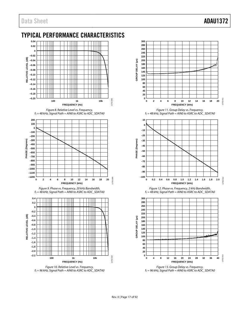
TYPICAL PERFORMANCE CHARACTERISTICS
Figure 8. Relative Level vs. Frequency,
fS = 48 kHz, Signal Path = AIN0 to ASRC to ADC_SDATA0
Figure 9. Phase vs. Frequency, 20 kHz Bandwidth,
fS = 48 kHz, Signal Path = AIN0 to ASRC to ADC_SDATA0
Figure 10. Relative Level vs. Frequency,
fS = 96 kHz, Signal Path = AIN0 to ASRC to ADC_SDATA0
Figure 11. Group Delay vs. Frequency,
fS = 48 kHz, Signal Path = AIN0 to ASRC to ADC_SDATA0
Figure 12. Phase vs. Frequency, 2 kHz Bandwidth,
fS = 48 kHz, Signal Path = AIN0 to ASRC to ADC_SDATA0
Figure 13. Group Delay vs. Frequency,
fS = 96 kHz, Signal Path = AIN0 to ASRC to ADC_SDATA0
0.04
–0.20
–0.18
–0.16
–0.14
–0.12
–0.10
–0.08
–0.06
–0.04
–0.02
0
0.02
100 1k 10k
REL
ATI
VE L
EVEL
(dB
)
FREQUENCY (Hz) 1270
2-00
8
200
–1200–1100–1000
–900–800–700–600–500–400–300–200–100
0100
0 2 4 6 8 10 12 14 16 18 20
PHA
SE (D
egre
es)
FREQUENCY (kHz) 1270
2-00
9
0.4
–2.2
–2.0
–1.8
–1.6
–1.4
–1.2
–1.0
–0.8
–0.6
–0.4
–0.2
0
0.2
100 1k 10k
REL
ATI
VE L
EVEL
(dB
)
FREQUENCY (Hz) 1270
2-01
0
300280260240220200180160140120100806040200
0 2 4 6 8 10 12 14 16 18 20
GR
OU
P D
ELA
Y (µ
s)
FREQUENCY (kHz) 1270
2-01
1
10
–100
–90
–80
–70
–60
–50
–40
–30
–20
–10
0
0 0.2 0.4 0.6 0.8 1.0 1.2 1.4 1.6 1.8 2.0
PHA
SE (D
egre
es)
FREQUENCY (kHz) 1270
2-01
2
300280260240220200180160140120100806040200
0 4 8 12 16 20 24 28 32 36 40
GR
OU
P D
ELA
Y (µ
s)
FREQUENCY (kHz) 1270
2-01
3
Rev. 0 | Page 17 of 92
ADAU1372 Data Sheet
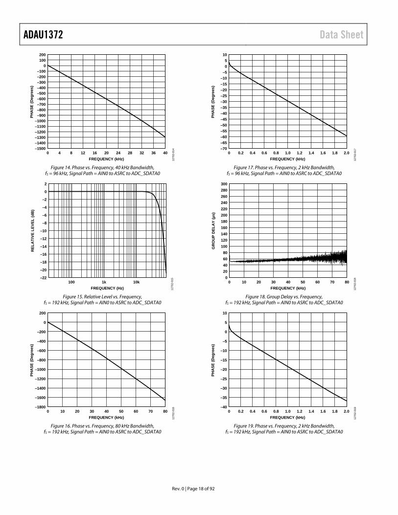
Figure 14. Phase vs. Frequency, 40 kHz Bandwidth,
fS = 96 kHz, Signal Path = AIN0 to ASRC to ADC_SDATA0
Figure 15. Relative Level vs. Frequency,
fS = 192 kHz, Signal Path = AIN0 to ASRC to ADC_SDATA0
Figure 16. Phase vs. Frequency, 80 kHz Bandwidth,
fS = 192 kHz, Signal Path = AIN0 to ASRC to ADC_SDATA0
Figure 17. Phase vs. Frequency, 2 kHz Bandwidth,
fS = 96 kHz, Signal Path = AIN0 to ASRC to ADC_SDATA0
Figure 18. Group Delay vs. Frequency,
fS = 192 kHz, Signal Path = AIN0 to ASRC to ADC_SDATA0
Figure 19. Phase vs. Frequency, 2 kHz Bandwidth,
fS = 192 kHz, Signal Path = AIN0 to ASRC to ADC_SDATA0
200
–1500–1400–1300–1200–1100–1000
–900–800–700–600–500–400–300–200–100
0100
0 4 8 12 16 20 24 28 32 36 40
PHA
SE (D
egre
es)
FREQUENCY (kHz) 1270
2-01
4
2
–22
–20
–18
–16
–14
–12
–10
–8
–6
–4
–2
0
10k100 1k
REL
ATI
VE L
EVEL
(dB
)
FREQUENCY (Hz) 1270
2-01
5
200
–1800
–1600
–1400
–1200
–1000
–800
–600
–400
–200
0
800 10 20 30 40 50 60 70
PHA
SE (D
egre
es)
FREQUENCY (kHz) 1270
2-01
6
10
–70–65–60–55–50–45–40–35–30–25–20–15–10–505
0 0.2 0.4 0.6 0.8 1.0 1.2 1.4 1.6 1.8 2.0
PHA
SE (D
egre
es)
FREQUENCY (kHz) 1270
2-01
7
300
020406080
100120140160180
220
260280
200
240
0 10 20 30 40 50 60 70 80
GR
OU
P D
ELA
Y (µ
s)
FREQUENCY (kHz) 1270
2-01
8
10
–40
–35
–30
–25
–20
–15
–10
–5
0
5
0 0.2 0.4 0.6 0.8 1.0 1.2 1.4 1.6 1.8 2.0
PHA
SE (D
egre
es)
FREQUENCY (kHz) 1270
2-01
9
Rev. 0 | Page 18 of 92
Data Sheet ADAU1372
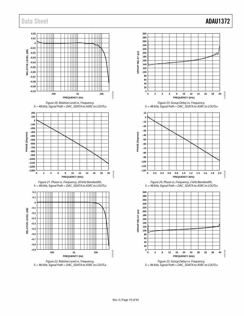
Figure 20. Relative Level vs. Frequency,
fS = 48 kHz, Signal Path = DAC_SDATA to ASRC to LOUTLx
Figure 21. Phase vs. Frequency, 20 kHz Bandwidth,
fS = 48 kHz, Signal Path = DAC_SDATA to ASRC to LOUTLx
Figure 22. Relative Level vs. Frequency,
fS = 96 kHz, Signal Path = DAC_SDATA to ASRC to LOUTLx
Figure 23. Group Delay vs. Frequency,
fS = 48 kHz, Signal Path = DAC_SDATA to ASRC to LOUTLx
Figure 24. Phase vs. Frequency, 2 kHz Bandwidth,
fS = 48 kHz, Signal Path = DAC_SDATA to ASRC to LOUTLx
Figure 25. Group Delay vs. Frequency,
fS = 96 kHz, Signal Path = DAC_SDATA to ASRC to LOUTLx
0.02
–0.10
–0.09
–0.08
–0.07
–0.06
–0.05
–0.04
–0.03
–0.02
–0.01
0
0.01
100 1k 10k
REL
ATI
VE L
EVEL
(dB
)
FREQUENCY (Hz) 1270
2-02
0200
–1300–1200–1100–1000
–900–800–700–600–500–400–300–200
1000
–100
PHA
SE (D
egre
es)
FREQUENCY (kHz)0 2 4 6 8 10 12 14 16 18 20
1270
2-02
1
0.2
–0.9
–0.8
–0.7
–0.6
–0.5
–0.4
–0.3
–0.2
–0.1
0
0.1
100 1k 10k
REL
ATI
VE L
EVEL
(dB
)
FREQUENCY (Hz) 1270
2-02
2
300
020406080
100120140160180200220240260280
GR
OU
P D
ELA
Y (µ
s)
FREQUENCY (kHz)0 2 4 6 8 10 12 14 16 18 20
1270
2-02
3
10
–120
–110
–100
–90
–80
–70
–60
–50
–40
–30
–20
0
–10
PHA
SE (D
egre
es)
FREQUENCY (kHz)0 0.2 0.4 0.6 0.8 1.0 1.2 1.4 1.6 1.8 2.0
1270
2-02
4
300
020406080
100120140160180200220240260280
GR
OU
P D
ELA
Y (µ
s)
FREQUENCY (kHz)0 4 8 12 16 20 24 28 32 36 40
1270
2-02
5
Rev. 0 | Page 19 of 92
ADAU1372 Data Sheet
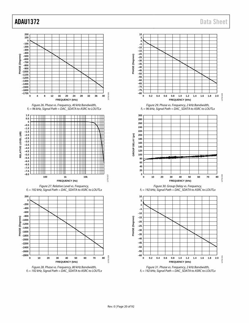
Figure 26. Phase vs. Frequency, 40 kHz Bandwidth,
fS = 96 kHz, Signal Path = DAC_SDATA to ASRC to LOUTLx
Figure 27. Relative Level vs. Frequency,
fS = 192 kHz, Signal Path = DAC_SDATA to ASRC to LOUTLx
Figure 28. Phase vs. Frequency, 80 kHz Bandwidth,
fS = 192 kHz, Signal Path = DAC_SDATA to ASRC to LOUTLx
Figure 29. Phase vs. Frequency, 2 kHz Bandwidth,
fS = 96 kHz, Signal Path = DAC_SDATA to ASRC to LOUTLx
Figure 30. Group Delay vs. Frequency,
fS = 192 kHz, Signal Path = DAC_SDATA to ASRC to LOUTLx
Figure 31. Phase vs. Frequency, 2 kHz Bandwidth,
fS = 192 kHz, Signal Path = DAC_SDATA to ASRC to LOUTLx
200
–1700–1600–1500–1400–1300–1200–1100–1000
–900–800–700–600–500–400–300–200–100
0100
PHA
SE (D
egre
es)
FREQUENCY (kHz)0 4 8 12 16 20 24 28 32 36 40
1270
2-02
6
1.0
–8.0–7.5–7.0–6.5–6.0–5.5–5.0–4.5–4.0–3.5–3.0–2.5–2.0–1.5–1.0–0.5
00.5
REL
ATI
VE L
EVEL
(dB
)
FREQUENCY (Hz)100 1k 10k
1270
2-02
7
200
–2800–2600–2400–2200–2000–1800–1600–1400–1200–1000
–600
–2000
–800
–400
0 10 20 30 40 50 60 70 80
PHA
SE (D
egre
es)
FREQUENCY (kHz) 1270
2-02
8
10
–80–75–70–65–60–55–50–45–40–35–30–25–20–15–10–505
PHA
SE (D
egre
es)
FREQUENCY (kHz)0 0.2 0.4 0.6 0.8 1.0 1.2 1.4 1.6 1.8 2.0
1270
2-02
9
300
020406080
100120140160180200220240260280
800 10 20 30 40 50 60 70
GR
OU
P D
ELA
Y (µ
s)
FREQUENCY (kHz) 1270
2-03
0
10
–60–55–50–45–40–35–30–25–20–15–10–5
05
PHA
SE (D
egre
es)
FREQUENCY (kHz)0 0.2 0.4 0.6 0.8 1.0 1.2 1.4 1.6 1.8 2.0
1270
2-03
1
Rev. 0 | Page 20 of 92
Data Sheet ADAU1372
Rev. 0 | Page 21 of 92
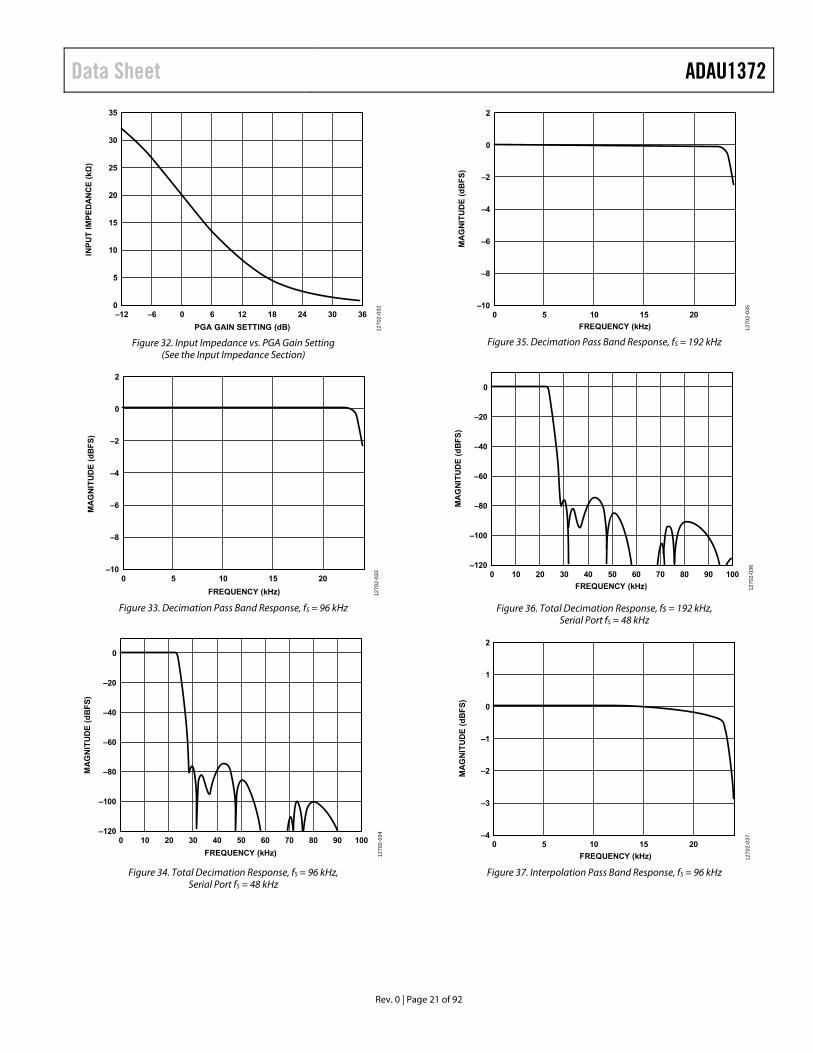
Figure 32. Input Impedance vs. PGA Gain Setting (See the Input Impedance Section)
Figure 33. Decimation Pass Band Response, fS = 96 kHz
Figure 34. Total Decimation Response, fS = 96 kHz, Serial Port fS = 48 kHz
Figure 35. Decimation Pass Band Response, fS = 192 kHz
Figure 36. Total Decimation Response, fs = 192 kHz, Serial Port fS = 48 kHz
Figure 37. Interpolation Pass Band Response, fS = 96 kHz
35
30
25
20
15
10
5
0
INP
UT
IM
PE
DA
NC
E (
kΩ)
PGA GAIN SETTING (dB)
–12 –6 0 6 12 18 24 30 36
1270
2-03
22
–10
–8
–6
–4
–2
0
0 2015105
MA
GN
ITU
DE
(d
BF
S)
FREQUENCY (kHz) 1270
2-03
3
–120
–100
–80
–60
–40
–20
0
0 100908070605040302010
MA
GN
ITU
DE
(d
BF
S)
FREQUENCY (kHz) 1270
2-03
4
2
–10
–8
–6
–4
–2
0
0 2015105
MA
GN
ITU
DE
(d
BF
S)
FREQUENCY (kHz) 1270
2-03
5
–120
–100
–80
–60
–40
–20
0
0 100908070605040302010
MA
GN
ITU
DE
(d
BF
S)
FREQUENCY (kHz) 1270
2-03
6
2
–4
–3
–2
–1
0
1
0 2015105
MA
GN
ITU
DE
(d
BF
S)
FREQUENCY (kHz) 1270
2-03
7
ADAU1372 Data Sheet
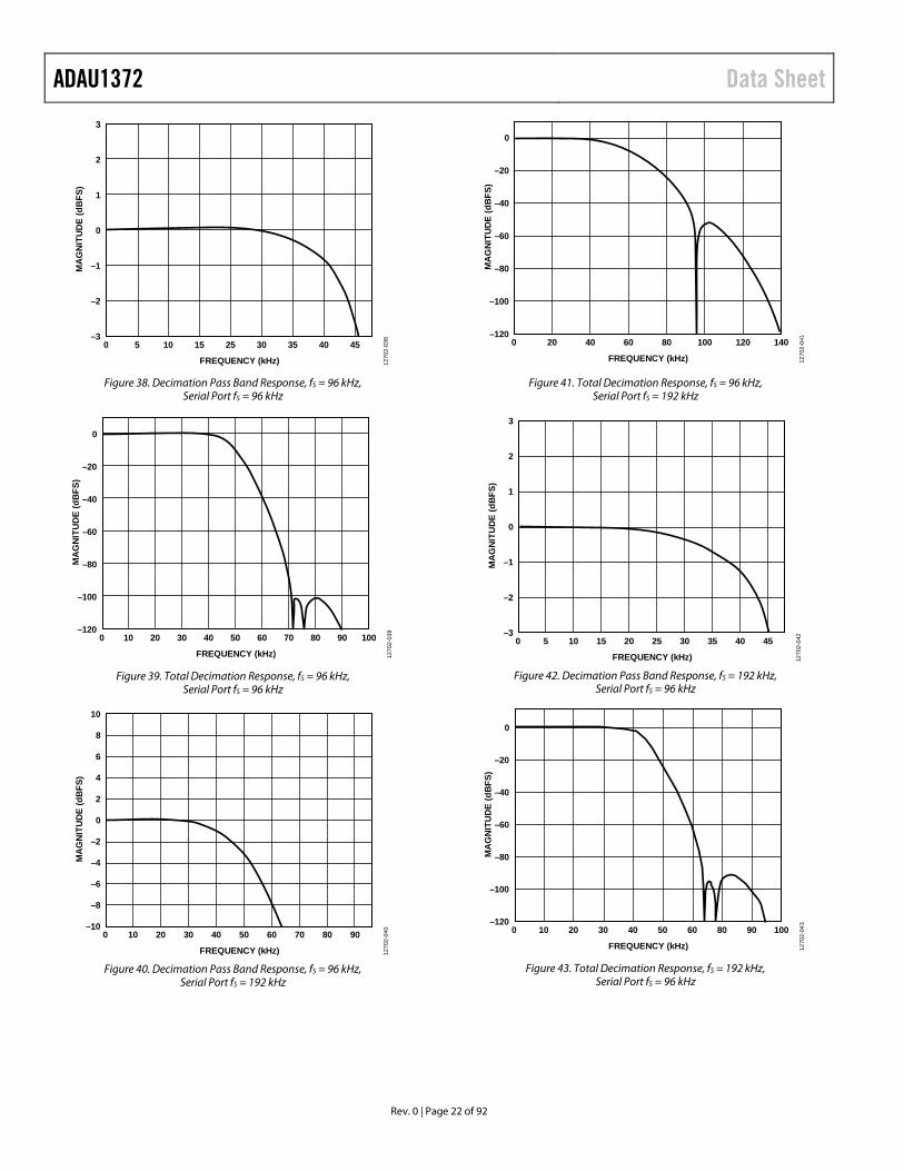
Figure 38. Decimation Pass Band Response, fS = 96 kHz, Serial Port fS = 96 kHz
Figure 39. Total Decimation Response, fS = 96 kHz, Serial Port fS = 96 kHz
Figure 40. Decimation Pass Band Response, fS = 96 kHz,
Serial Port fS = 192 kHz
Figure 41. Total Decimation Response, fS = 96 kHz, Serial Port fS = 192 kHz
Figure 42. Decimation Pass Band Response, fS = 192 kHz,
Serial Port fS = 96 kHz
Figure 43. Total Decimation Response, fS = 192 kHz, Serial Port fS = 96 kHz
–3
–2
–1
0
1
2
3
0 4540353025
FREQUENCY (kHz)
15105
MA
GN
ITU
DE
(dB
FS)
1270
2-03
8
–120
–100
–80
–60
–40
–20
0
0 10090807060
FREQUENCY (kHz)
50402010 30
MA
GN
ITU
DE
(dB
FS)
1270
2-03
9
–10
–6
–8
8
–4
–2
2
4
6
0
10
0 90807060
FREQUENCY (kHz)
50402010 30
MA
GN
ITU
DE
(dB
FS)
1270
2-04
0
–120
–100
–60
–80
0
–40
–20
0 140120
FREQUENCY (kHz)
100804020 60
MA
GN
ITU
DE
(dB
FS)
1270
2-04
1
–3
–2
0
–1
3
1
2
0 4530 35 40
FREQUENCY (kHz)
2520105 15
MA
GN
ITU
DE
(dB
FS)
1270
2-04
2
–120
–100
–60
–80
0
–40
–20
0 10090
FREQUENCY (kHz)
806040302010 50
MA
GN
ITU
DE
(dB
FS)
1270
2-04
3
Rev. 0 | Page 22 of 92
Data Sheet ADAU1372
Rev. 0 | Page 23 of 92
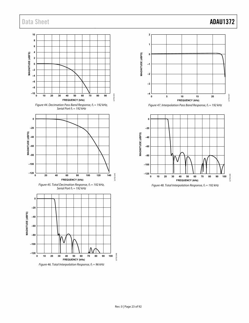
Figure 44. Decimation Pass Band Response, fS = 192 kHz, Serial Port fS = 192 kHz
Figure 45. Total Decimation Response, fS = 192 kHz, Serial Port fS = 192 kHz
Figure 46. Total Interpolation Response, fS = 96 kHz
Figure 47. Interpolation Pass Band Response, fS = 192 kHz
Figure 48. Total Interpolation Response, fS = 192 kHz
–10
–6
–8
8
–4
–2
2
4
6
0
10
0 90807060
FREQUENCY (kHz)
50402010 30
MA
GN
ITU
DE
(d
BF
S)
1270
2-04
4
–120
–100
–80
–60
–40
–20
0
0 1401201008060
FREQUENCY (kHz)
4020
MA
GN
ITU
DE
(d
BF
S)
1270
2-04
5
–120
–100
–80
–60
–40
–20
0
0 100908070605040302010
MA
GN
ITU
DE
(d
BF
S)
FREQUENCY (kHz) 1270
2-04
6
2
–4
–3
–2
–1
0
1
MA
GN
ITU
DE
(d
BF
S)
FREQUENCY (kHz)
0 2015105
1270
2-04
7
–120
–100
–80
–60
–40
–20
0
0 100908070605040302010
MA
GN
ITU
DE
(d
BF
S)
FREQUENCY (kHz) 1270
2-04
8
ADAU1372 Data Sheet
THEORY OF OPERATION The ADAU1372 is a low power audio codec that is ideal for portable applications that require high quality audio, low power, small size, and low latency. The four ADC and two DAC channels each have an SNR of at least 94 dB and a THD + N of at least −88 dB. The serial data port is compatible with I2S, left justified, right justified, and TDM modes, with tristating for interfacing to digital audio data. The operating voltage range is 1.8 V to 3.3 V, with an on-board regulator generating the internal digital supply voltage. If desired, the regulator can be powered down and the voltage can be supplied externally.
The input signal path includes flexible configurations that can accept single-ended analog microphone inputs as well as up to four channels of digital microphone inputs. Two microphone bias pins provide seamless interfacing to electret microphones. Each input signal has its own PGA for volume adjustment.
The ADCs and DACs are high quality, 24-bit Σ-Δ converters that operate at a selectable 192 kHz or 96 kHz sampling rate. The ADCs have an optional high-pass filter with a cutoff frequency of 1 Hz, 4 Hz, or 8 Hz. The ADCs and DACs also include very fine step digital volume controls.
The stereo DAC output can differentially drive a headphone earpiece speaker with 16 Ω impedance or higher. One side of the differential output can be powered down if single-ended operation is required. There is also the option to change to line output mode when the output is lightly loaded.
The SigmaStudio™ software can be used to control the registers through the control port. SigmaStudio allows an easy graphical interface to control the signal flow; the tool can be used to configure all of the ADAU1372 registers.
The ADAU1372 can generate its internal clocks from a wide range of input clocks by using the on-board fractional PLL. The PLL accepts inputs from 8 MHz to 27 MHz. For standalone operation, the clock can be generated using the on-board crystal oscillator.
The ADAU1372 is provided in a small, 40-lead, 6 mm × 6 mm LFCSP with an exposed bottom pad.
Rev. 0 | Page 24 of 92
Data Sheet ADAU1372
SYSTEM CLOCKING AND POWER-UP INITIALIZATION The ADAU1372 must be powered up and initialized in the proper sequence. The power-up details are outlined in the Power Sequencing section. After power up, the clocks must be properly configured and applied before writing to any registers addresses above Register 0x06. See the Clock Initialization section for details.
After the clocks are enabled, the ADCs, DACs, and multifunction pins can be set up for the desired operation.
Finally, the serial ports and ASRCs must be set up and initialized. See the Serial Port Initialization section for more details.
CLOCK INITIALIZATION The ADAU1372 can generate its clocks either from an externally provided clock or from a crystal oscillator. In both cases, the on-board PLL can be used or the clock can be fed directly to the internal blocks. When a crystal oscillator is used, it is desirable to use a 12.288 MHz crystal, and the crystal oscillator function must be enabled in the MCLK_EN bit (Register 0x00, Bit 0). If the PLL is used, it must always be set to output 24.576 MHz. The PLL can be bypassed if a clock of 12.288 MHz or 24.576 MHz is available in the system. Bypassing the PLL saves system power.
Set the CC_MDIV bit (Register 0x00, Bit 1) such that the internal master clock is always 12.288 MHz; for example, when using a 24.576 MHz external source clock or if using the PLL, it is necessary to use the internal divide by 2 (see Table 11).
The CC_MDIV bit must not be changed after setup; however, the CLKSRC bit (Register 0x00, Bit 3) can be switched while the internal master clock is enabled.
Table 11. Clock Configuration Settings CC_MDIV Description 1 Divide the PLL/external clock by 1. Use this setting
for a 12.288 MHz direct input clock source. 0 Divide the PLL/external clock by 2. Use this setting
for a 24.576 MHz direct input clock source or if using the PLL.
PLL Bypass Setup
On power up, the ADAU1372 exits an internal reset after 12 ms. The rate of the internal master clock must be set properly using the CC_MDIV bit in the clock control register. When bypassing the PLL, the clock fed into the MCLKIN pin must be either 12.288 MHz or 24.576 MHz. The internal master clock of the ADAU1372 is disabled and no register writes can be performed above Register 0x06 until the MCLK_EN bit is asserted.
PLL Enabled Setup
The internal master clock of the ADAU1372 is disabled by the default setting of the MCLK_EN bit and must remain disabled during the PLL lock acquisition period. The user can poll the lock bit (Register 0x06, Bit 0) to determine when the PLL has locked. After lock is acquired, the ADAU1372 can be started by asserting the MCLK_EN bit. This bit enables the master clock for all the internal blocks of the ADAU1372.
To program the PLL during initialization or reconfiguration of the codec, the following procedure must be followed:
1. Ensure that PLL_EN (Register 0x00, Bit 7) is set low. 2. Set or reset the PLL control registers (Register 0x01 to
Register 0x05). 3. Enable the PLL using the PLL_EN bit. 4. Poll the PLL lock bit (Register 0x06, Bit 0). 5. Set the MCLK_EN bit in Register 0x00 after PLL lock is
acquired.
Control Port Access During Initialization
During the lock acquisition period, only Register 0x00 to Register 0x06 are accessible through the control port. A read or write to any other register is prohibited until the master clock enable bit and the lock bit are both asserted.
PLL The PLL uses the MCLKIN signal as a reference to generate the internal master clock (MCLK). The PLL settings are set in Register 0x00 to Register 0x05. Depending on the MCLK frequency, the PLL must be set for either integer or fractional mode. The PLL can accept input frequencies in the range of 8 MHz to 27 MHz.
Figure 49. PLL Block Diagram
Input Clock Divider
Before reaching the PLL, the input clock signal goes through an integer clock divider to ensure that the clock frequency is within a suitable range for the PLL. The X bits in the PLL_CTRL4 register (Register 0x05, Bits[2:1]) set the PLL input clock divide ratio.
Integer Mode
Integer mode is used when the clock input is an integer multiple of the PLL output.
For example, if MCLKIN = 12.288 MHz and (X + 1) = 1, and fS = 48 kHz, then
PLL Required Output = 24.576 MHz
R/2 = 24.576 MHz/12.288 MHz = 2
where R/2 = 2 or R = 4.
MCLK ÷X × (R + N/M)
TO PLLCLOCK DIVIDER
1270
2-05
0
Rev. 0 | Page 25 of 92
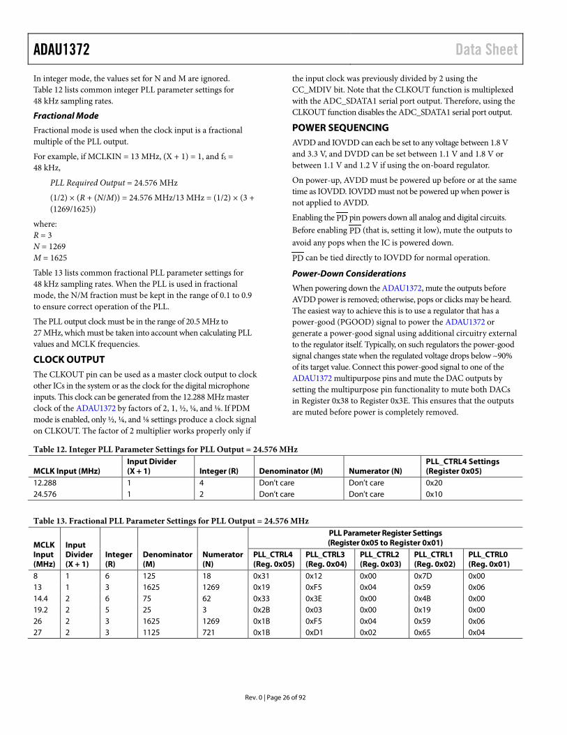
ADAU1372 Data Sheet In integer mode, the values set for N and M are ignored. Table 12 lists common integer PLL parameter settings for 48 kHz sampling rates.
Fractional Mode
Fractional mode is used when the clock input is a fractional multiple of the PLL output.
For example, if MCLKIN = 13 MHz, (X + 1) = 1, and fS = 48 kHz,
PLL Required Output = 24.576 MHz
(1/2) × (R + (N/M)) = 24.576 MHz/13 MHz = (1/2) × (3 + (1269/1625))
where: R = 3 N = 1269 M = 1625
Table 13 lists common fractional PLL parameter settings for 48 kHz sampling rates. When the PLL is used in fractional mode, the N/M fraction must be kept in the range of 0.1 to 0.9 to ensure correct operation of the PLL.
The PLL output clock must be in the range of 20.5 MHz to 27 MHz, which must be taken into account when calculating PLL values and MCLK frequencies.
CLOCK OUTPUT The CLKOUT pin can be used as a master clock output to clock other ICs in the system or as the clock for the digital microphone inputs. This clock can be generated from the 12.288 MHz master clock of the ADAU1372 by factors of 2, 1, ½, ¼, and ⅛. If PDM mode is enabled, only ½, ¼, and ⅛ settings produce a clock signal on CLKOUT. The factor of 2 multiplier works properly only if
the input clock was previously divided by 2 using the CC_MDIV bit. Note that the CLKOUT function is multiplexed with the ADC_SDATA1 serial port output. Therefore, using the CLKOUT function disables the ADC_SDATA1 serial port output.
POWER SEQUENCING AVDD and IOVDD can each be set to any voltage between 1.8 V and 3.3 V, and DVDD can be set between 1.1 V and 1.8 V or between 1.1 V and 1.2 V if using the on-board regulator.
On power-up, AVDD must be powered up before or at the same time as IOVDD. IOVDD must not be powered up when power is not applied to AVDD.
Enabling the PD pin powers down all analog and digital circuits. Before enabling PD (that is, setting it low), mute the outputs to avoid any pops when the IC is powered down.
PD can be tied directly to IOVDD for normal operation.
Power-Down Considerations
When powering down the ADAU1372, mute the outputs before AVDD power is removed; otherwise, pops or clicks may be heard. The easiest way to achieve this is to use a regulator that has a power-good (PGOOD) signal to power the ADAU1372 or generate a power-good signal using additional circuitry external to the regulator itself. Typically, on such regulators the power-good signal changes state when the regulated voltage drops below ~90% of its target value. Connect this power-good signal to one of the ADAU1372 multipurpose pins and mute the DAC outputs by setting the multipurpose pin functionality to mute both DACs in Register 0x38 to Register 0x3E. This ensures that the outputs are muted before power is completely removed.
Table 12. Integer PLL Parameter Settings for PLL Output = 24.576 MHz
MCLK Input (MHz) Input Divider (X + 1) Integer (R) Denominator (M) Numerator (N)
PLL_CTRL4 Settings (Register 0x05)
12.288 1 4 Don’t care Don’t care 0x20 24.576 1 2 Don’t care Don’t care 0x10
Table 13. Fractional PLL Parameter Settings for PLL Output = 24.576 MHz
MCLK Input (MHz)
Input Divider (X + 1)
PLL Parameter Register Settings (Register 0x05 to Register 0x01)
Integer (R)
Denominator (M)
Numerator (N)
PLL_CTRL4 (Reg. 0x05)
PLL_CTRL3 (Reg. 0x04)
PLL_CTRL2 (Reg. 0x03)
PLL_CTRL1 (Reg. 0x02)
PLL_CTRL0 (Reg. 0x01)
8 1 6 125 18 0x31 0x12 0x00 0x7D 0x00 13 1 3 1625 1269 0x19 0xF5 0x04 0x59 0x06 14.4 2 6 75 62 0x33 0x3E 0x00 0x4B 0x00 19.2 2 5 25 3 0x2B 0x03 0x00 0x19 0x00 26 2 3 1625 1269 0x1B 0xF5 0x04 0x59 0x06 27 2 3 1125 721 0x1B 0xD1 0x02 0x65 0x04
Rev. 0 | Page 26 of 92
Data Sheet ADAU1372
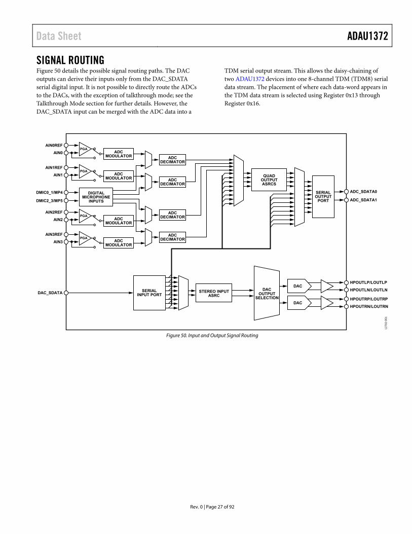
Rev. 0 | Page 27 of 92
SIGNAL ROUTING Figure 50 details the possible signal routing paths. The DAC outputs can derive their inputs only from the DAC_SDATA serial digital input. It is not possible to directly route the ADCs to the DACs, with the exception of talkthrough mode; see the Talkthrough Mode section for further details. However, the DAC_SDATA input can be merged with the ADC data into a
TDM serial output stream. This allows the daisy-chaining of two ADAU1372 devices into one 8-channel TDM (TDM8) serial data stream. The placement of where each data-word appears in the TDM data stream is selected using Register 0x13 through Register 0x16.
Figure 50. Input and Output Signal Routing
AIN0REF
AIN0PGA
AIN1REF
AIN1PGA
AIN2REF
AIN2PGA
AIN3REF
AIN3PGA
DMIC0_1/MP4
DMIC2_3/MP5
DIGITALMICROPHONE
INPUTS
ADCMODULATOR
ADCMODULATOR
ADCMODULATOR ADC
DECIMATOR
ADCDECIMATOR
ADCDECIMATOR
ADCDECIMATOR
ADCMODULATOR
HPOUTLN/LOUTLN
HPOUTLP/LOUTLP
HPOUTRN/LOUTRN
ADC_SDATA0
ADC_SDATA1
HPOUTRP/LOUTRP
DACOUTPUT
SELECTION
SERIALINPUT PORT
QUADOUTPUTASRCS
1270
2-05
1
DAC_SDATA
DAC
DAC
STEREO INPUTASRC
SERIALOUTPUT
PORT
ADAU1372 Data Sheet
Rev. 0 | Page 28 of 92
INPUT SIGNAL PATHS Four input paths, from either an ADC or a digital microphone, can be routed to the quad output ASRC. The input sources (ADC or digital microphone) must be configured in pairs (for example, 0 and 1 or 2 and 3), but each channel can be routed individually. The serial input data can also be routed to the serial output port which allows the daisy-chaining of two ADAU1372 devices to combine eight channels of ADC inputs onto one TDM8 stream. The DAC_SDATA serial inputs can also be routed to the quad output ASRCs, but it is not recommended. The output ASRCs add 2.5 dB of gain; the sample rate does not need to be converted, and there are only four channels of ASRC.
ANALOG INPUTS The ADAU1372 can accept both line level and microphone inputs. Each of the four analog input channels can be configured in a single-ended mode or a single-ended with PGA mode. There are also inputs for up to four digital microphones. The analog inputs are biased at AVDD/2. Connect unused input pins to the CM pin or ac-couple them to ground.
Signal Polarity
Signals routed through the PGAs are inverted. As a result, signals input through the PGA are output from the ADCs with a polarity that is opposite that of the input. Single-ended inputs are not inverted. The ADCs are noninverting.
Input Impedance
The input impedance of the analog inputs varies with the gain of the PGA. This impedance ranges from 0.68 kΩ at the +35.25 dB gain setting to 32.0 kΩ at the −12 dB setting. The input impedance on each pin, RIN, can be calculated as follows:
kΩ110
40)20/(
GainINR
where Gain is set by PGA_GAINx.
The optional 10 dB PGA boost set in the PGA_x_BOOST bits does not affect the input impedance. This is an alternative way of increasing gain without decreasing input impedance; however, it causes some degradation in performance.
Analog Microphone Inputs
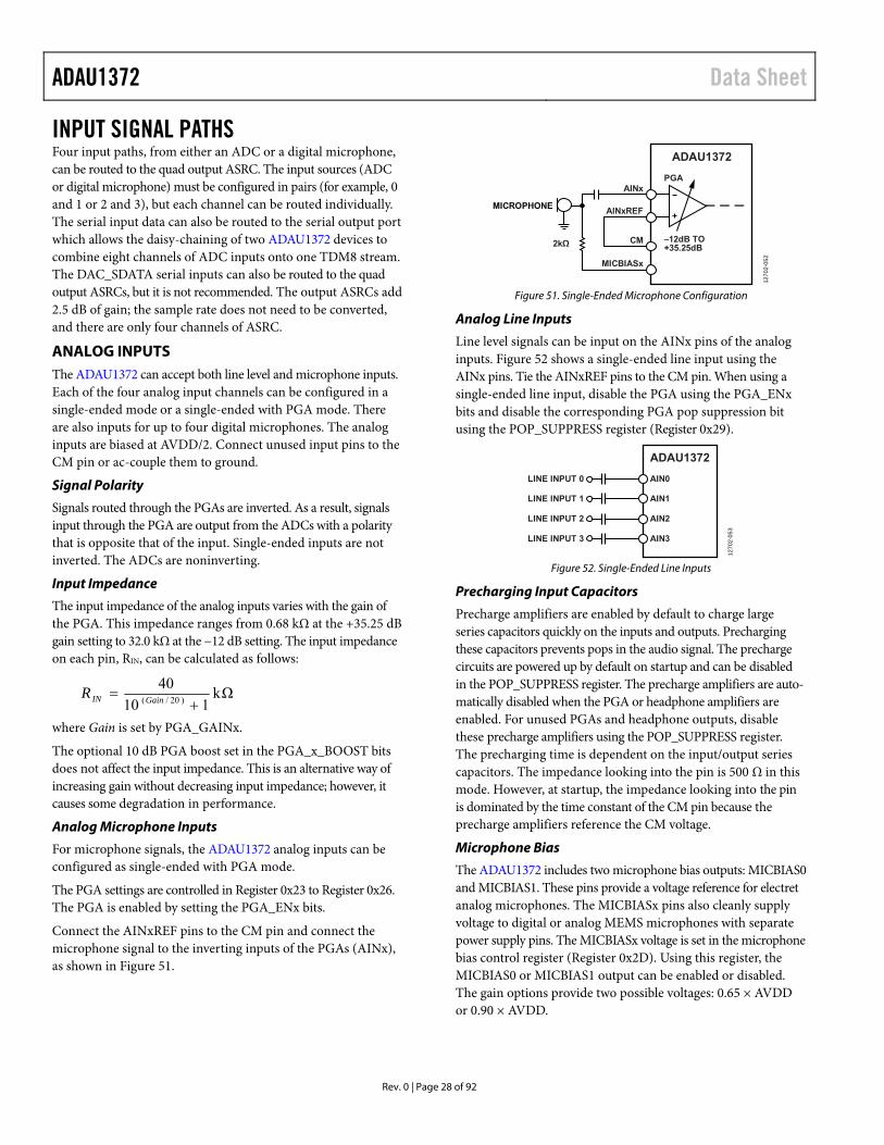
For microphone signals, the ADAU1372 analog inputs can be configured as single-ended with PGA mode.
The PGA settings are controlled in Register 0x23 to Register 0x26. The PGA is enabled by setting the PGA_ENx bits.
Connect the AINxREF pins to the CM pin and connect the microphone signal to the inverting inputs of the PGAs (AINx), as shown in Figure 51.
Figure 51. Single-Ended Microphone Configuration
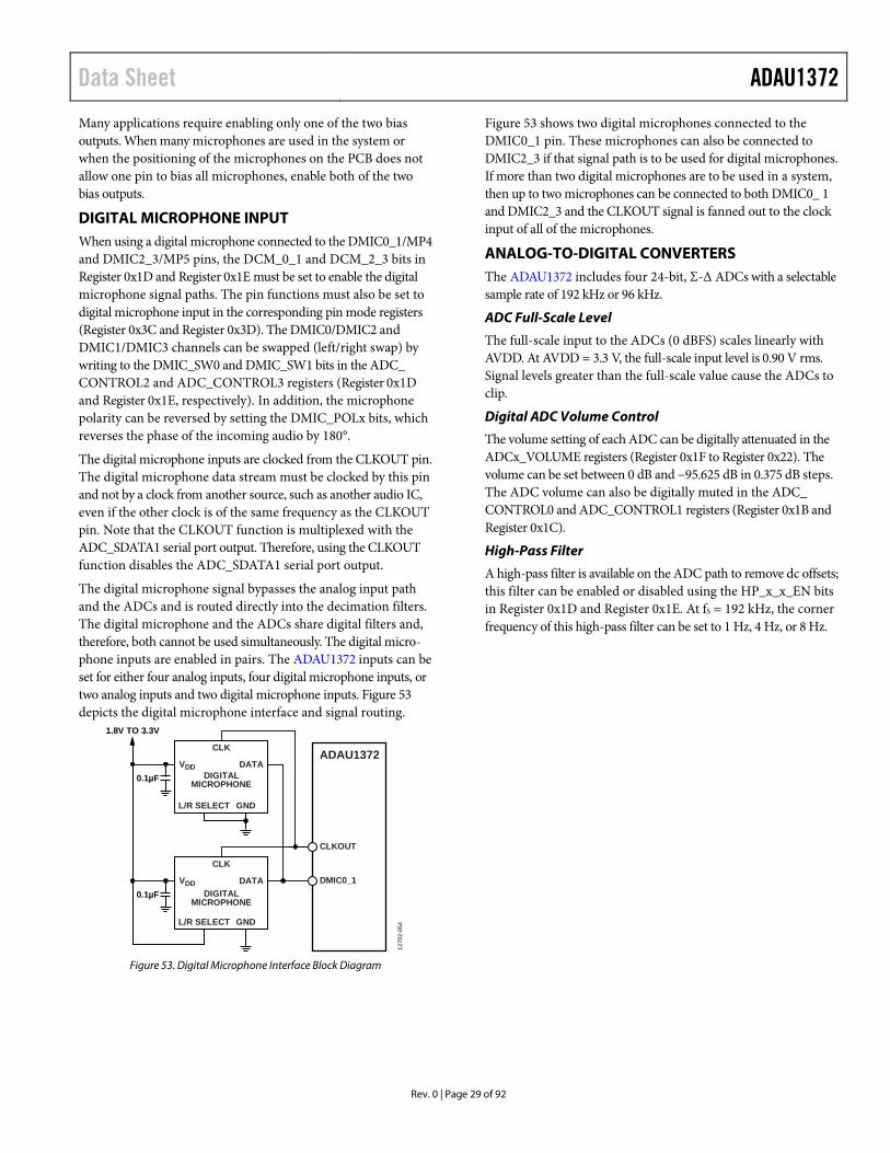
Analog Line Inputs
Line level signals can be input on the AINx pins of the analog inputs. Figure 52 shows a single-ended line input using the AINx pins. Tie the AINxREF pins to the CM pin. When using a single-ended line input, disable the PGA using the PGA_ENx bits and disable the corresponding PGA pop suppression bit using the POP_SUPPRESS register (Register 0x29).
Figure 52. Single-Ended Line Inputs
Precharging Input Capacitors
Precharge amplifiers are enabled by default to charge large series capacitors quickly on the inputs and outputs. Precharging these capacitors prevents pops in the audio signal. The precharge circuits are powered up by default on startup and can be disabled in the POP_SUPPRESS register. The precharge amplifiers are auto-matically disabled when the PGA or headphone amplifiers are enabled. For unused PGAs and headphone outputs, disable these precharge amplifiers using the POP_SUPPRESS register. The precharging time is dependent on the input/output series capacitors. The impedance looking into the pin is 500 Ω in this mode. However, at startup, the impedance looking into the pin is dominated by the time constant of the CM pin because the precharge amplifiers reference the CM voltage.
Microphone Bias
The ADAU1372 includes two microphone bias outputs: MICBIAS0 and MICBIAS1. These pins provide a voltage reference for electret analog microphones. The MICBIASx pins also cleanly supply voltage to digital or analog MEMS microphones with separate power supply pins. The MICBIASx voltage is set in the microphone bias control register (Register 0x2D). Using this register, the MICBIAS0 or MICBIAS1 output can be enabled or disabled. The gain options provide two possible voltages: 0.65 × AVDD or 0.90 × AVDD.
MICROPHONE
PGA
–12dB TO+35.25dB
ADAU1372
AINx
AINxREF
MICBIASx
CM2kΩ
1270
2-05
2
ADAU1372
LINE INPUT 0 AIN0
LINE INPUT 1 AIN1
LINE INPUT 2 AIN2
LINE INPUT 3 AIN3
1270
2-05
3
Data Sheet ADAU1372 Many applications require enabling only one of the two bias outputs. When many microphones are used in the system or when the positioning of the microphones on the PCB does not allow one pin to bias all microphones, enable both of the two bias outputs.
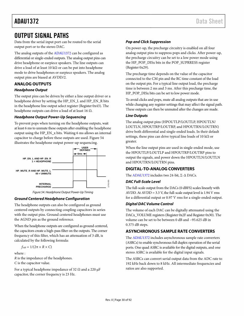
DIGITAL MICROPHONE INPUT When using a digital microphone connected to the DMIC0_1/MP4 and DMIC2_3/MP5 pins, the DCM_0_1 and DCM_2_3 bits in Register 0x1D and Register 0x1E must be set to enable the digital microphone signal paths. The pin functions must also be set to digital microphone input in the corresponding pin mode registers (Register 0x3C and Register 0x3D). The DMIC0/DMIC2 and DMIC1/DMIC3 channels can be swapped (left/right swap) by writing to the DMIC_SW0 and DMIC_SW1 bits in the ADC_ CONTROL2 and ADC_CONTROL3 registers (Register 0x1D and Register 0x1E, respectively). In addition, the microphone polarity can be reversed by setting the DMIC_POLx bits, which reverses the phase of the incoming audio by 180°.
The digital microphone inputs are clocked from the CLKOUT pin. The digital microphone data stream must be clocked by this pin and not by a clock from another source, such as another audio IC, even if the other clock is of the same frequency as the CLKOUT pin. Note that the CLKOUT function is multiplexed with the ADC_SDATA1 serial port output. Therefore, using the CLKOUT function disables the ADC_SDATA1 serial port output.
The digital microphone signal bypasses the analog input path and the ADCs and is routed directly into the decimation filters. The digital microphone and the ADCs share digital filters and, therefore, both cannot be used simultaneously. The digital micro-phone inputs are enabled in pairs. The ADAU1372 inputs can be set for either four analog inputs, four digital microphone inputs, or two analog inputs and two digital microphone inputs. Figure 53 depicts the digital microphone interface and signal routing.
Figure 53. Digital Microphone Interface Block Diagram
Figure 53 shows two digital microphones connected to the DMIC0_1 pin. These microphones can also be connected to DMIC2_3 if that signal path is to be used for digital microphones. If more than two digital microphones are to be used in a system, then up to two microphones can be connected to both DMIC0_ 1 and DMIC2_3 and the CLKOUT signal is fanned out to the clock input of all of the microphones.
ANALOG-TO-DIGITAL CONVERTERS The ADAU1372 includes four 24-bit, Σ-Δ ADCs with a selectable sample rate of 192 kHz or 96 kHz.
ADC Full-Scale Level
The full-scale input to the ADCs (0 dBFS) scales linearly with AVDD. At AVDD = 3.3 V, the full-scale input level is 0.90 V rms. Signal levels greater than the full-scale value cause the ADCs to clip.
Digital ADC Volume Control
The volume setting of each ADC can be digitally attenuated in the ADCx_VOLUME registers (Register 0x1F to Register 0x22). The volume can be set between 0 dB and −95.625 dB in 0.375 dB steps. The ADC volume can also be digitally muted in the ADC_ CONTROL0 and ADC_CONTROL1 registers (Register 0x1B and Register 0x1C).
High-Pass Filter
A high-pass filter is available on the ADC path to remove dc offsets; this filter can be enabled or disabled using the HP_x_x_EN bits in Register 0x1D and Register 0x1E. At fS = 192 kHz, the corner frequency of this high-pass filter can be set to 1 Hz, 4 Hz, or 8 Hz.
ADAU1372
CLKOUT
DMIC0_1
DIGITALMICROPHONE
CLK
VDD DATA
L/R SELECT GND
0.1µF
DIGITALMICROPHONE
CLK
VDD DATA
L/R SELECT GND
0.1µF
1.8V TO 3.3V
1270
2-05
4
Rev. 0 | Page 29 of 92
ADAU1372 Data Sheet
OUTPUT SIGNAL PATHS Data from the serial input port can be routed to the serial output port or to the stereo DAC.
The analog outputs of the ADAU1372 can be configured as differential or single-ended outputs. The analog output pins can drive headphone or earpiece speakers. The line outputs can drive a load of at least 10 kΩ or can be put into headphone mode to drive headphones or earpiece speakers. The analog output pins are biased at AVDD/2.
ANALOG OUTPUTS Headphone Output
The output pins can be driven by either a line output driver or a headphone driver by setting the HP_EN_L and HP_EN_R bits in the headphone line output select register (Register 0x43). The headphone outputs can drive a load of at least 16 Ω.
Headphone Output Power-Up Sequencing
To prevent pops when turning on the headphone outputs, wait at least 6 ms to unmute these outputs after enabling the headphone output using the HP_EN_x bits. Waiting 6 ms allows an internal capacitor to charge before these outputs are used. Figure 54 illustrates the headphone output power-up sequencing.
Figure 54. Headphone Output Power-Up Timing
Ground Centered Headphone Configuration
The headphone outputs can also be configured as ground centered outputs by connecting coupling capacitors in series with the output pins. Ground centered headphones must use the AGND pin as the ground reference.
When the headphone outputs are configured as ground centered, the capacitors create a high-pass filter on the outputs. The corner frequency of this filter, which has an attenuation of 3 dB, is calculated by the following formula:
f3dB = 1/(2π × R × C)
where : R is the impedance of the headphones. C is the capacitor value.
For a typical headphone impedance of 32 Ω and a 220 µF capacitor, the corner frequency is 23 Hz.
Pop and Click Suppression
On power-up, the precharge circuitry is enabled on all four analog output pins to suppress pops and clicks. After power-up, the precharge circuitry can be set to a low power mode using the HP_POP_DISx bits in the POP_SUPRRESS register (Register 0x29).
The precharge time depends on the value of the capacitor connected to the CM pin and the RC time constant of the load on the output pin. For a typical line output load, the precharge time is between 2 ms and 3 ms. After this precharge time, the HP_POP_DISx bits can be set to low power mode.
To avoid clicks and pops, mute all analog outputs that are in use while changing any register settings that may affect the signal path. These outputs can then be unmuted after the changes are made.
Line Outputs
The analog output pins (HPOUTLP/LOUTLP, HPOUTLN/ LOUTLN, HPOUTRP/LOUTRP, and HPOUTRN/LOUTRN) drive both differential and single-ended loads. In their default settings, these pins can drive typical line loads of 10 kΩ or greater.
When the line output pins are used in single-ended mode, use the HPOUTLP/LOUTLP and HPOUTRP/LOUTRP pins to output the signals, and power down the HPOUTLN/LOUTLN and HPOUTRN/LOUTRN pins.
DIGITAL-TO-ANALOG CONVERTERS The ADAU1372 includes two 24-bit, Σ-Δ DACs.
DAC Full-Scale Level
The full-scale output from the DACs (0 dBFS) scales linearly with AVDD. At AVDD = 3.3 V, the full-scale output level is 1.94 V rms for a differential output or 0.97 V rms for a single-ended output.
Digital DAC Volume Control
The volume of each DAC can be digitally attenuated using the DACx_VOLUME registers (Register 0x2F and Register 0x30). The volume can be set to be between 0 dB and −95.625 dB in 0.375 dB steps.
ASYNCHRONOUS SAMPLE RATE CONVERTERS The ADAU1372 includes asynchronous sample rate converters (ASRCs) to enable synchronous full duplex operation of the serial ports. One quad ASRC is available for the digital outputs, and one stereo ASRC is available for the digital input signals.
The ASRCs can convert serial output data from the ADC rate to 192 kHz back down to 8 kHz. All intermediate frequencies and ratios are also supported.
HP_EN_L AND HP_EN_R1 = HEADPHONE
HP_MUTE_R AND HP_MUTE_L00 = UNMUTE
INTERNALPRECHARGE
6ms
USERDEFINED
1270
2-05
5
Rev. 0 | Page 30 of 92
Data Sheet ADAU1372
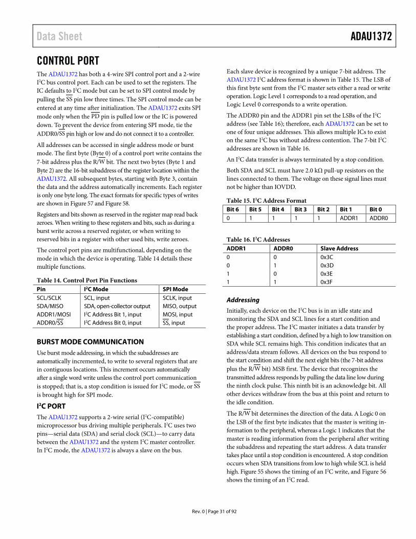
CONTROL PORT The ADAU1372 has both a 4-wire SPI control port and a 2-wire I2C bus control port. Each can be used to set the registers. The IC defaults to I2C mode but can be set to SPI control mode by pulling the SS pin low three times. The SPI control mode can be entered at any time after initialization. The ADAU1372 exits SPI mode only when the PD pin is pulled low or the IC is powered down. To prevent the device from entering SPI mode, tie the ADDR0/SS pin high or low and do not connect it to a controller.
All addresses can be accessed in single address mode or burst mode. The first byte (Byte 0) of a control port write contains the 7-bit address plus the R/W bit. The next two bytes (Byte 1 and Byte 2) are the 16-bit subaddress of the register location within the ADAU1372. All subsequent bytes, starting with Byte 3, contain the data and the address automatically increments. Each register is only one byte long. The exact formats for specific types of writes are shown in Figure 57 and Figure 58.
Registers and bits shown as reserved in the register map read back zeroes. When writing to these registers and bits, such as during a burst write across a reserved register, or when writing to reserved bits in a register with other used bits, write zeroes.
The control port pins are multifunctional, depending on the mode in which the device is operating. Table 14 details these multiple functions.
Table 14. Control Port Pin Functions Pin I2C Mode SPI Mode SCL/SCLK SCL, input SCLK, input SDA/MISO SDA, open-collector output MISO, output ADDR1/MOSI I2C Address Bit 1, input MOSI, input ADDR0/SS I2C Address Bit 0, input SS, input
BURST MODE COMMUNICATION Use burst mode addressing, in which the subaddresses are automatically incremented, to write to several registers that are in contiguous locations. This increment occurs automatically after a single word write unless the control port communication is stopped; that is, a stop condition is issued for I2C mode, or SS is brought high for SPI mode.
I2C PORT The ADAU1372 supports a 2-wire serial (I2C-compatible) microprocessor bus driving multiple peripherals. I2C uses two pins—serial data (SDA) and serial clock (SCL)—to carry data between the ADAU1372 and the system I2C master controller. In I2C mode, the ADAU1372 is always a slave on the bus.
Each slave device is recognized by a unique 7-bit address. The ADAU1372 I2C address format is shown in Table 15. The LSB of this first byte sent from the I2C master sets either a read or write operation. Logic Level 1 corresponds to a read operation, and Logic Level 0 corresponds to a write operation.
The ADDR0 pin and the ADDR1 pin set the LSBs of the I2C address (see Table 16); therefore, each ADAU1372 can be set to one of four unique addresses. This allows multiple ICs to exist on the same I2C bus without address contention. The 7-bit I2C addresses are shown in Table 16.
An I2C data transfer is always terminated by a stop condition.
Both SDA and SCL must have 2.0 kΩ pull-up resistors on the lines connected to them. The voltage on these signal lines must not be higher than IOVDD.
Table 15. I2C Address Format Bit 6 Bit 5 Bit 4 Bit 3 Bit 2 Bit 1 Bit 0 0 1 1 1 1 ADDR1 ADDR0
Table 16. I2C Addresses ADDR1 ADDR0 Slave Address 0 0 0x3C 0 1 0x3D 1 0 0x3E 1 1 0x3F
Addressing
Initially, each device on the I2C bus is in an idle state and monitoring the SDA and SCL lines for a start condition and the proper address. The I2C master initiates a data transfer by establishing a start condition, defined by a high to low transition on SDA while SCL remains high. This condition indicates that an address/data stream follows. All devices on the bus respond to the start condition and shift the next eight bits (the 7-bit address plus the R/W bit) MSB first. The device that recognizes the transmitted address responds by pulling the data line low during the ninth clock pulse. This ninth bit is an acknowledge bit. All other devices withdraw from the bus at this point and return to the idle condition.
The R/W bit determines the direction of the data. A Logic 0 on the LSB of the first byte indicates that the master is writing in-formation to the peripheral, whereas a Logic 1 indicates that the master is reading information from the peripheral after writing the subaddress and repeating the start address. A data transfer takes place until a stop condition is encountered. A stop condition occurs when SDA transitions from low to high while SCL is held high. Figure 55 shows the timing of an I2C write, and Figure 56 shows the timing of an I2C read.
Rev. 0 | Page 31 of 92
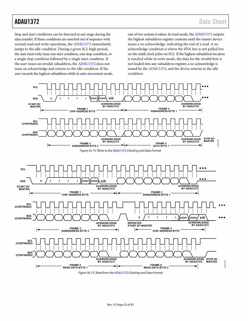
ADAU1372 Data Sheet
Rev. 0 | Page 32 of 92
Stop and start conditions can be detected at any stage during the data transfer. If these conditions are asserted out of sequence with normal read and write operations, the ADAU1372 immediately jumps to the idle condition. During a given SCL high period, the user must only issue one start condition, one stop condition, or a single stop condition followed by a single start condition. If the user issues an invalid subaddress, the ADAU1372 does not issue an acknowledge and returns to the idle condition. If the user exceeds the highest subaddress while in auto-increment mode,
one of two actions is taken. In read mode, the ADAU1372 outputs the highest subaddress register contents until the master device issues a no acknowledge, indicating the end of a read. A no acknowledge condition is where the SDA line is not pulled low on the ninth clock pulse on SCL. If the highest subaddress location is reached while in write mode, the data for the invalid byte is not loaded into any subaddress register, a no acknowledge is issued by the ADAU1372, and the device returns to the idle condition.
Figure 55. I2C Write to the ADAU1372 Clocking and Data Format
Figure 56. I2C Read from the ADAU1372 Clocking and Data Format
R/W0
SCL
SDA
SDA(CONTINUED)
SCL(CONTINUED)
1 1 1 ADDR0ADDR11
START BYMASTER
FRAME 1CHIP ADDRESS BYTE
FRAME 2SUBADDRESS BYTE 1
FRAME 3SUBADDRESS BYTE 2
FRAME 4DATA BYTE 1
ACKNOWLEDGEBY ADAU1372
ACKNOWLEDGEBY ADAU1372
ACKNOWLEDGEBY ADAU1372
ACKNOWLEDGEBY ADAU1372
STOP BYMASTER
1270
2-05
6R/W
SCL
SDA
SDA(CONTINUED)
SCL(CONTINUED)
SDA(CONTINUED)
SCL(CONTINUED)
START BYMASTER
FRAME 2SUBADDRESS BYTE 1
FRAME 3SUBADDRESS BYTE 2
FRAME 4CHIP ADDRESS BYTE
FRAME 1CHIP ADDRESS BYTE
FRAME 5READ DATA BYTE 1
FRAME 6READ DATA BYTE 2
ACKNOWLEDGEBY ADAU1372
ACKNOWLEDGEBY ADAU1372
ACKNOWLEDGEBY ADAU1372
ACKNOWLEDGEBY ADAU1372
ACKNOWLEDGEBY ADAU1372
STOP BYMASTER
ACKNOWLEDGEBY ADAU1372
REPEATEDSTART BY MASTER
R/W
ADDR0
ADDR0ADDR1
ADDR1
0 1 1 1 1
0 1 1 1 1
1270
2-05
7
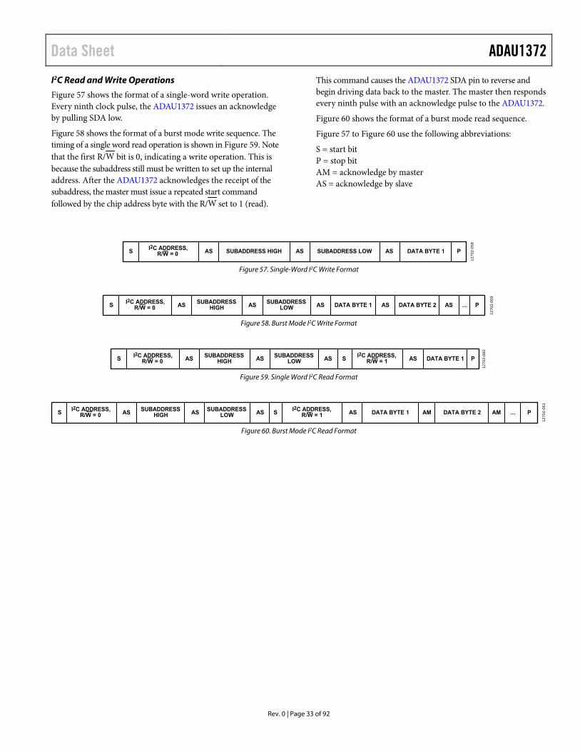
Data Sheet ADAU1372
Rev. 0 | Page 33 of 92
I2C Read and Write Operations
Figure 57 shows the format of a single-word write operation. Every ninth clock pulse, the ADAU1372 issues an acknowledge by pulling SDA low.
Figure 58 shows the format of a burst mode write sequence. The timing of a single word read operation is shown in Figure 59. Note that the first R/W bit is 0, indicating a write operation. This is because the subaddress still must be written to set up the internal address. After the ADAU1372 acknowledges the receipt of the subaddress, the master must issue a repeated start command followed by the chip address byte with the R/W set to 1 (read).
This command causes the ADAU1372 SDA pin to reverse and begin driving data back to the master. The master then responds every ninth pulse with an acknowledge pulse to the ADAU1372.
Figure 60 shows the format of a burst mode read sequence.
Figure 57 to Figure 60 use the following abbreviations:
S = start bit P = stop bit AM = acknowledge by master AS = acknowledge by slave
Figure 57. Single-Word I2C Write Format
Figure 58. Burst Mode I2C Write Format
Figure 59. Single Word I2C Read Format
Figure 60. Burst Mode I2C Read Format
S I2C ADDRESS,R/W = 0 AS SUBADDRESS HIGH AS SUBADDRESS LOW AS DATA BYTE 1 P
1270
2-05
8
...S I2C ADDRESS,R/W = 0 AS SUBADDRESS
HIGH AS SUBADDRESSLOW AS DATA BYTE 1 DATA BYTE 2 AS PAS
1270
2-05
9
DATA BYTE 1 PS I2C ADDRESS,R/W = 0 AS SUBADDRESS
HIGH AS SUBADDRESSLOW AS I2C ADDRESS,
R/W = 1 ASS
1270
2-06
0
...DATA BYTE 1 DATA BYTE 2AM AM PS I2C ADDRESS,R/W = 0 AS SUBADDRESS
HIGH AS SUBADDRESSLOW AS I2C ADDRESS,
R/W = 1 ASS
1270
2-06
1
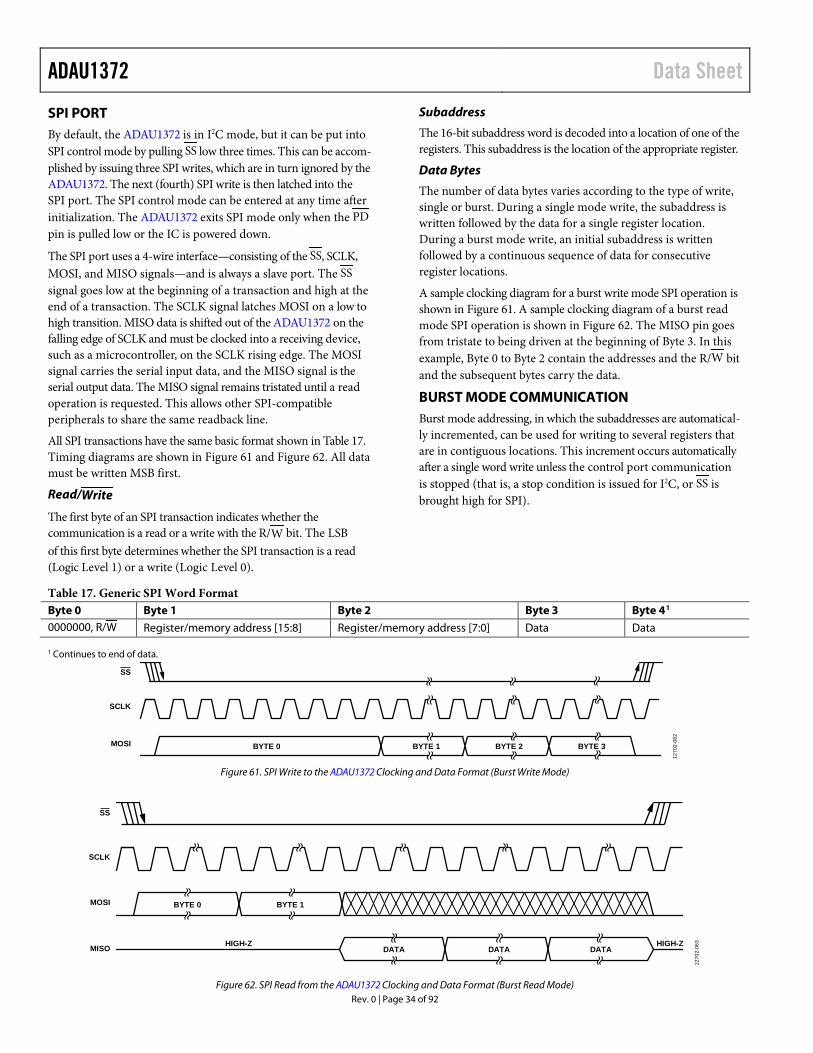
ADAU1372 Data Sheet
SPI PORT By default, the ADAU1372 is in I2C mode, but it can be put into SPI control mode by pulling SS low three times. This can be accom-plished by issuing three SPI writes, which are in turn ignored by the ADAU1372. The next (fourth) SPI write is then latched into the SPI port. The SPI control mode can be entered at any time after initialization. The ADAU1372 exits SPI mode only when the PDpin is pulled low or the IC is powered down.
The SPI port uses a 4-wire interface—consisting of the SS, SCLK, MOSI, and MISO signals—and is always a slave port. The SS signal goes low at the beginning of a transaction and high at the end of a transaction. The SCLK signal latches MOSI on a low to high transition. MISO data is shifted out of the ADAU1372 on the falling edge of SCLK and must be clocked into a receiving device, such as a microcontroller, on the SCLK rising edge. The MOSI signal carries the serial input data, and the MISO signal is the serial output data. The MISO signal remains tristated until a read operation is requested. This allows other SPI-compatible peripherals to share the same readback line.
All SPI transactions have the same basic format shown in Table 17. Timing diagrams are shown in Figure 61 and Figure 62. All data must be written MSB first.
Read/Write
The first byte of an SPI transaction indicates whether the communication is a read or a write with the R/W bit. The LSB of this first byte determines whether the SPI transaction is a read (Logic Level 1) or a write (Logic Level 0).
Subaddress
The 16-bit subaddress word is decoded into a location of one of the registers. This subaddress is the location of the appropriate register.
Data Bytes
The number of data bytes varies according to the type of write, single or burst. During a single mode write, the subaddress is written followed by the data for a single register location. During a burst mode write, an initial subaddress is written followed by a continuous sequence of data for consecutive register locations.
A sample clocking diagram for a burst write mode SPI operation is shown in Figure 61. A sample clocking diagram of a burst read mode SPI operation is shown in Figure 62. The MISO pin goes from tristate to being driven at the beginning of Byte 3. In this example, Byte 0 to Byte 2 contain the addresses and the R/W bit and the subsequent bytes carry the data.
BURST MODE COMMUNICATION Burst mode addressing, in which the subaddresses are automatical-ly incremented, can be used for writing to several registers that are in contiguous locations. This increment occurs automatically after a single word write unless the control port communication is stopped (that is, a stop condition is issued for I2C, or SS is brought high for SPI).
Table 17. Generic SPI Word Format Byte 0 Byte 1 Byte 2 Byte 3 Byte 41 0000000, R/W Register/memory address [15:8] Register/memory address [7:0] Data Data
1 Continues to end of data.
Figure 61. SPI Write to the ADAU1372 Clocking and Data Format (Burst Write Mode)
Figure 62. SPI Read from the ADAU1372 Clocking and Data Format (Burst Read Mode)
SS
SCLK
MOSI BYTE 0 BYTE 1 BYTE 2 BYTE 3
1270
2-06
2
SS
SCLK
MOSI
MISO
BYTE 0 BYTE 1
DATA DATA DATAHIGH-ZHIGH-Z
1270
2-06
3
Rev. 0 | Page 34 of 92
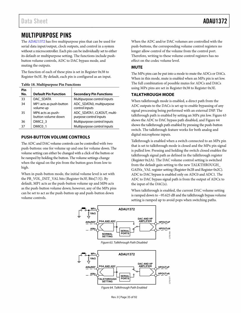
Data Sheet ADAU1372
Rev. 0 | Page 35 of 92
MULTIPURPOSE PINS The ADAU1372 has five multipurpose pins that can be used for serial data input/output, clock outputs, and control in a system without a microcontroller. Each pin can be individually set to either its default or multipurpose setting. The functions include push-button volume controls, ADC to DAC bypass mode, and muting the outputs.
The function of each of these pins is set in Register 0x38 to Register 0x3E. By default, each pin is configured as an input.
Table 18. Multipurpose Pin Functions Pin No. Default Pin Function Secondary Pin Functions 33 DAC_SDATA Multipurpose control inputs 34 MP1 acts as push-button
volume up ADC_SDATA0, multipurpose control inputs
35 MP6 acts as push-button volume down
ADC_SDATA1, CLKOUT, multi-purpose control inputs
36 DMIC2_3 Multipurpose control inputs 37 DMIC0_1 Multipurpose control inputs
PUSH-BUTTON VOLUME CONTROLS The ADC and DAC volume controls can be controlled with two push-buttons: one for volume up and one for volume down. The volume setting can either be changed with a click of the button or be ramped by holding the button. The volume settings change when the signal on the pin from the button goes from low to high.
When in push-button mode, the initial volume level is set with the PB_VOL_INIT_VAL bits (Register 0x3F, Bits[7:3]). By default, MP1 acts as the push-button volume up and MP6 acts as the push-button volume down; however, any of the MPx pins can be set to act as the push-button up and push-button down volume controls.
When the ADC and/or DAC volumes are controlled with the push-buttons, the corresponding volume control registers no longer allow control of the volume from the control port. Therefore, writing to these volume control registers has no effect on the codec volume level.
MUTE The MPx pins can be put into a mode to mute the ADCs or DACs. When in this mode, mute is enabled when an MPx pin is set low. The full combination of possible mutes for ADCs and DACs using MPx pins are set in Register 0x38 to Register 0x3E.
TALKTHROUGH MODE When talkthrough mode is enabled, a direct path from the ADC outputs to the DACs is set up to enable bypassing of any signal processing being performed with an external DSP. The talkthrough path is enabled by setting an MPx pin low. Figure 63 shows the ADC to DAC bypass path disabled, and Figure 64 shows the talkthrough path enabled by pressing the push-button switch. The talkthrough feature works for both analog and digital microphone inputs.
Talkthrough is enabled when a switch connected to an MPx pin that is set to talkthrough mode is closed and the MPx pin signal is pulled low. Pressing and holding the switch closed enables the talkthrough signal path as defined in the talkthrough register (Register 0x2A). The DAC volume control setting is switched from the default gain setting to the new TALKTHROUGH_ GAINx_VAL register setting (Register 0x2B and Register 0x2C). ADC to DAC bypass is enabled only on ADC0 and ADC1. The ADC to DAC bypass signal path is from the output of ADCx to the input of the DAC(s).
When talkthrough is enabled, the current DAC volume setting is ramped down to −95.625 dB and the talkthrough bypass volume setting is ramped up to avoid pops when switching paths.
Figure 63. Talkthrough Path Disabled
Figure 64. Talkthrough Path Enabled
ADAU1372
PGA AND ADCDAC AND HPAMPLIFIER
NORMALSETTING
HPOUTxP
HPOUTxN
10kΩ
MPx
AINxREF
AINx
1270
2-06
4SERIALPORTS
ADAU1372
PGA AND ADCDAC AND HPAMPLIFIER
TALKTHROUGHSETTING
HPOUTxP
HPOUTxN
10kΩ
MPx
AINxREF
AINx
1270
2-07
7SERIALPORTS
ADAU1372 Data Sheet
SERIAL DATA INPUT/OUTPUT PORTS The serial data input and output ports of the ADAU1372 can be set to accept or transmit data in a 2-channel format or in a 4-channel or 8-channel TDM stream mode to interface to external ADCs, DACs, DSPs, and systems on chip (SOCs). Data is processed in twos complement, MSB first format. The left channel data field always precedes the right channel data field in the 2-channel streams. In 8-channel TDM mode, the data channels are output sequentially, starting with the channel set by the ADC_SDATA0_ST and ADC_SDATA1_ST bits. The serial modes and the position of the data in the frame are set in the serial data port (SAI_0, SAI_1) and serial output control registers (SOUT_SOURCE_x_x, Register 0x13 to Register 0x16).
The serial data clocks do not need to be synchronous with the ADAU1372 master clock input, but the LRCLK and BCLK clocks must be synchronous to each other. The LRCLK and BCLK pins both clock the serial input and output ports. The ADAU1372 can be set to be either the master or the slave in a system. Because there is only one set of serial data clocks, the input and output ports must always both be either master or slave.
The serial data control registers allow control of the clock polarity and the data input modes. The valid data formats are I2S, left justified, right justified (24- or 16-bit), PCM, and TDM. In all modes except for the right justified modes, the serial port inputs an arbitrary number of bits up to a limit of 24. Extra bits do not cause an error, but they are truncated internally.
The serial port can operate with an arbitrary number of BCLK transitions in each LRCLK frame. The LRCLK in TDM mode can be input to the ADAU1372 either as a 50% duty cycle clock or as a 1 bit wide pulse. Table 19 lists the modes in which the serial input/output port can function. When using low IOVDD (1.8 V) with a high BCLK rate (12.288 MHz), a sample rate of 192 kHz, or a TDM8 mode operating at a sample rate of 48 kHz, it is recommended to use the high drive settings on the serial port pins. The high drive strength effectively speeds up the transition times of the waveforms, thereby improving the signal integrity of the clock and data lines. These can be set in the PAD_CONTROL4 register (Register 0x4C).
Table 19. Serial Input/Output Port Master/Slave Mode Capabilities Serial Port fS (kHz)
2-Channel Modes (I2S, Left Justified, Right Justified)
4-Channel TDM
8-Channel TDM
48 Yes Yes Yes 96 Yes Yes No 192 Yes No No
Table 20 describes the proper serial port settings for standard audio data formats. More information about the settings in this table can be found in the Serial Port Control 0 register and the Serial Port Control 1 register (Register 0x32 and Register 0x33, respectively) descriptions.
SERIAL PORT INITIALIZATION After the clock initialization is complete and the MCLK_EN bit in Register 0x00 is enabled, the serial ports can be initialized and set up for the desired operational mode. See the System Clocking and Power-Up section for more details on clock initialization.
To initialize the ADC to serial data outputs ADC_SDATA0 and/or ADC_SDATA1, follow this procedure:
6. Set the MODE_MP1 register (Register 0x39) to 0x00 to enable Serial Output 0.
7. Set the MODE_MP6 register (Register 0x3E) to 0x00 to enable Serial Output 1.
8. Write 0xFF to the DECIM_PWR_MODES register (Register 0x44) to enable all the ASRCs and the sync filters.
9. Enable ADC0 and ADC1 in the ADC_CONTROL2 register (Register 0x1D).
10. Enable ADC2 and ADC3 in the ADC_CONTROL3 register (Register 0x1E).
11. Enable the output ASRCs in the ASRC_MODE register (Register 0x1A).
12. Select a source for the quad ASRCs using the ASRCO_ SOURCE_0_1 register (Register 0x18) and the ASRCO_ SOURCE_2_3 register (Register 0x19).
13. Unmute ADC0 and ADC1 in the ADC_CONTROL0 register (Register 0x1B).
14. Unmute ADC2 and ADC3 in the ADC_CONTROL1 register (Register 0x1C).
To initialize the serial data inputs to appear at the DAC outputs, follow this procedure:
1. Enable ASRC and DAC modulator power using the INTERP_PWR_MODES register (Register 0x45).
2. Enable the input ASRCs in the ASRC_MODE register (Register 0x1A).
3. Select DAC0 and DAC1 as the source for the input ASRCs in the DAC_SOURCE_0_1 register (Register 0x11).
4. Enable the DACs in the DAC_CONTROL1 register (Register 0x2E).
5. Enable the power to the HPOUTLP/LOUTLP output and the HPOUTLN/LOUTLN output in the OP_STAGE_CTRL register (Register 0x43).
6. Unmute the DACs using the DAC_CONTROL1 register (Register 0x2E)
7. Unmute the headphone/line outputs using the OP_STAGE_MUTES register (Register 0x31).
Rev. 0 | Page 36 of 92
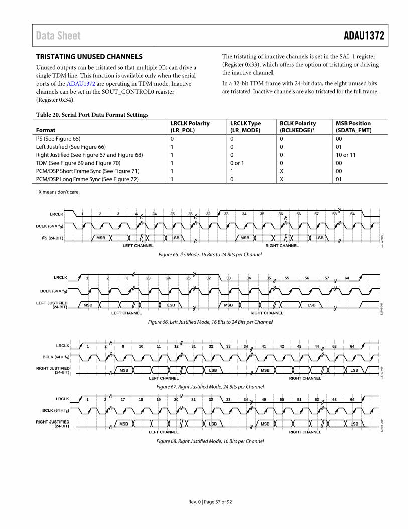
Data Sheet ADAU1372
TRISTATING UNUSED CHANNELS Unused outputs can be tristated so that multiple ICs can drive a single TDM line. This function is available only when the serial ports of the ADAU1372 are operating in TDM mode. Inactive channels can be set in the SOUT_CONTROL0 register (Register 0x34).
The tristating of inactive channels is set in the SAI_1 register (Register 0x33), which offers the option of tristating or driving the inactive channel.
In a 32-bit TDM frame with 24-bit data, the eight unused bits are tristated. Inactive channels are also tristated for the full frame.
Table 20. Serial Port Data Format Settings
Format LRCLK Polarity (LR_POL)
LRCLK Type (LR_MODE)
BCLK Polarity (BCLKEDGE)1
MSB Position (SDATA_FMT)
I2S (See Figure 65) 0 0 0 00 Left Justified (See Figure 66) 1 0 0 01 Right Justified (See Figure 67 and Figure 68) 1 0 0 10 or 11 TDM (See Figure 69 and Figure 70) 1 0 or 1 0 00 PCM/DSP Short Frame Sync (See Figure 71) 1 1 X 00 PCM/DSP Long Frame Sync (See Figure 72) 1 0 X 01 1 X means don’t care.
Figure 65. I2S Mode, 16 Bits to 24 Bits per Channel
Figure 66. Left Justified Mode, 16 Bits to 24 Bits per Channel
Figure 67. Right Justified Mode, 24 Bits per Channel
Figure 68. Right Justified Mode, 16 Bits per Channel
MSB LSB
LEFT CHANNEL
MSB LSB
RIGHT CHANNEL
LRCLK
BCLK (64 × fS)
I2S (24-BIT)
1 2 3 4 24 25 26 32 33 34 35 36 56 57 58 64
1270
2-06
6
MSB LSB
LEFT CHANNEL
MSB LSB
RIGHT CHANNEL
LRCLK
BCLK (64 × fS)
LEFT JUSTIFIED(24-BIT)
1 2 3 23 24 25 32 33 34 35 55 56 57 64
1270
2-06
7
LRCLK
BCLK (64 × fS)
RIGHT JUSTIFIED(24-BIT)
LEFT CHANNEL
MSB LSB
RIGHT CHANNEL
MSB LSB
1 2 9 10 11 12 31 32 33 34 41 42 43 44 63 64
1270
2-06
8
BCLK (64 × fS)
RIGHT JUSTIFIED(24-BIT)
LEFT CHANNEL
MSB LSB
RIGHT CHANNEL
MSB LSB
LRCLK 1 2 17 18 19 20 31 32 33 34 49 50 51 52 63 64
1270
2-06
9
Rev. 0 | Page 37 of 92
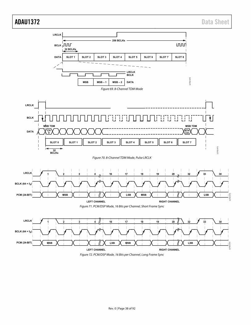
ADAU1372 Data Sheet
Rev. 0 | Page 38 of 92
Figure 69. 8-Channel TDM Mode
Figure 70. 8-Channel TDM Mode, Pulse LRCLK
Figure 71. PCM/DSP Mode, 16 Bits per Channel, Short Frame Sync
Figure 72. PCM/DSP Mode, 16 Bits per Channel, Long Frame Sync
256 BCLKs
32 BCLKs
LRCLK
BCLK
DATA
LRCLKBCLK
DATAMSB – 2MSB – 1MSB
SLOT 1 SLOT 2 SLOT 3 SLOT 4 SLOT 5 SLOT 6 SLOT 7 SLOT 8
1270
2-07
0
LRCLK
BCLK
DATA CH0
8THCH
MSB TDM MSB TDM
32BCLKs
SLOT 0 SLOT 1 SLOT 2 SLOT 3 SLOT 4 SLOT 5 SLOT 6 SLOT 7
1270
2-07
1
LEFT CHANNEL
MSB MSBLSB LSB
RIGHT CHANNEL
LRCLK
BCLK (64 × fS)
PCM (24-BIT)
1 2 3 4 16 17 18 19 20 32 33 34
1270
2-07
2
LRCLK
BCLK (64 × fS)
PCM (24-BIT)
LEFT CHANNEL
MSB MSBLSB LSB
RIGHT CHANNEL
1 2 3 4 16 17 18 19 20 32 33 34
1270
2-07
3
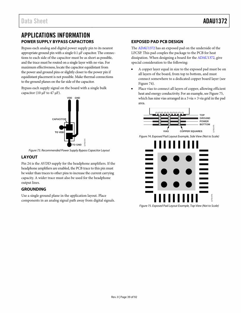
Data Sheet ADAU1372
APPLICATIONS INFORMATION POWER SUPPLY BYPASS CAPACITORS Bypass each analog and digital power supply pin to its nearest appropriate ground pin with a single 0.1 µF capacitor. The connec-tions to each side of the capacitor must be as short as possible, and the trace must be routed on a single layer with no vias. For maximum effectiveness, locate the capacitor equidistant from the power and ground pins or slightly closer to the power pin if equidistant placement is not possible. Make thermal connections to the ground planes on the far side of the capacitor.
Bypass each supply signal on the board with a single bulk capacitor (10 µF to 47 µF).
Figure 73. Recommended Power Supply Bypass Capacitor Layout
LAYOUT Pin 24 is the AVDD supply for the headphone amplifiers. If the headphone amplifiers are enabled, the PCB trace to this pin must be wider than traces to other pins to increase the current carrying capacity. A wider trace must also be used for the headphone output lines.
GROUNDING Use a single ground plane in the application layout. Place components in an analog signal path away from digital signals.
EXPOSED PAD PCB DESIGN The ADAU1372 has an exposed pad on the underside of the LFCSP. This pad couples the package to the PCB for heat dissipation. When designing a board for the ADAU1372, give special consideration to the following:
• A copper layer equal in size to the exposed pad must be on all layers of the board, from top to bottom, and must connect somewhere to a dedicated copper board layer (see Figure 74).
• Place vias to connect all layers of copper, allowing efficient heat and energy conductivity. For an example, see Figure 75, which has nine vias arranged in a 3 via × 3 via grid in the pad area.
Figure 74. Exposed Pad Layout Example, Side View (Not to Scale)
Figure 75. Exposed Pad Layout Example, Top View (Not to Scale)
VDD GND
TO GND
TO VDD
CAPACITOR
1270
2-07
4
TOP
POWERGROUND
BOTTOM
COPPER SQUARESVIAS 1270
2-07
512
702-
076
Rev. 0 | Page 39 of 92
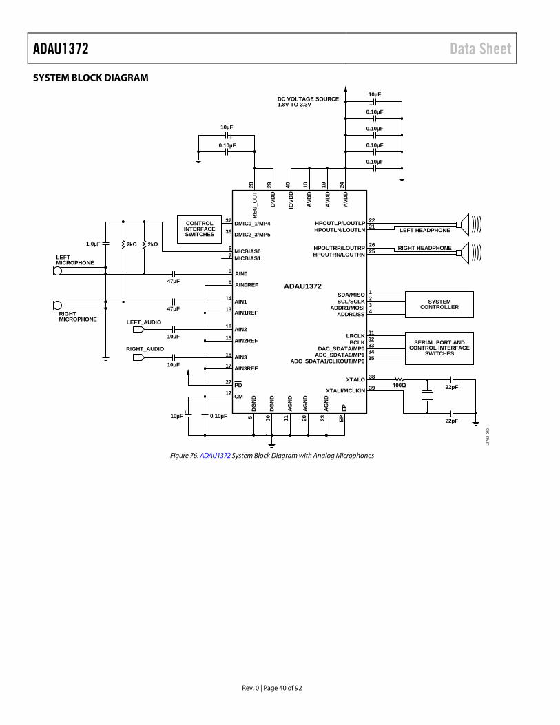
ADAU1372 Data Sheet
SYSTEM BLOCK DIAGRAM
Figure 76. ADAU1372 System Block Diagram with Analog Microphones
SYSTEMCONTROLLER
SERIAL PORT ANDCONTROL INTERFACE
SWITCHES
DC VOLTAGE SOURCE:1.8V TO 3.3V
LEFTMICROPHONE
RIGHTMICROPHONE
LEFT HEADPHONE
RIGHT HEADPHONE
1SDA/MISO 2SCL/SCLK 3ADDR1/MOSI 4ADDR0/SS
56 MICBIAS07 MICBIAS1
8 AIN0REF
9 AIN0
10A
VDD
11
13 AIN1REF
14 AIN1
15 AIN2REF
16 AIN2
12 CM
17 AIN3REF
18 AIN3
19A
VDD
20 23A
GN
D
AG
ND
AG
ND
DG
ND
24A
VDD
21HPOUTLN/LOUTLN
22HPOUTLP/LOUTLP
25HPOUTRN/LOUTRN
26HPOUTRP/LOUTRP
27 PD
40IO
VDD
28R
EG_O
UT
30
31LRCLK 32BCLK 33DAC_SDATA/MP0 34ADC_SDATA0/MP1
38XTALO39XTALI/MCLKIN
35ADC_SDATA1/CLKOUT/MP6
36 DMIC2_3/MP5
37 DMIC0_1/MP4
29D
VDD
EPEP
ADAU1372
100Ω 22pF
+
10µF
1.0µF
LEFT_AUDIO
RIGHT_AUDIO
CONTROLINTERFACESWITCHES
DG
ND
1270
2-04
9
10µF 0.10µF
0.10µF
0.10µF
0.10µF
0.10µF
22pF
47µF
47µF
10µF
10µF
2kΩ 2kΩ
+
+0.10µF
10µF
Rev. 0 | Page 40 of 92
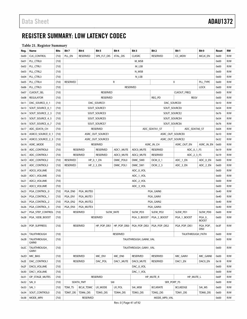
Data Sheet ADAU1372
REGISTER SUMMARY: LOW LATENCY CODEC Table 21. Register Summary
Reg. Name Bits Bit 7 Bit 6 Bit 5 Bit 4 Bit 3 Bit 2 Bit 1 Bit 0 Reset RW
0x00 CLK_CONTROL [7:0] PLL_EN RESERVED SPK_FLT_DIS XTAL_DIS CLKSRC RESERVED CC_MDIV MCLK_EN 0x00 R/W
0x01 PLL_CTRL0 [7:0] M_MSB 0x00 R/W
0x02 PLL_CTRL1 [7:0] M_LSB 0x00 R/W
0x03 PLL_CTRL2 [7:0] N_MSB 0x00 R/W
0x04 PLL_CTRL3 [7:0] N_LSB 0x00 R/W
0x05 PLL_CTRL4 [7:0] RESERVED R X PLL_TYPE 0x00 R/W
0x06 PLL_CTRL5 [7:0] RESERVED LOCK 0x00 R/W
0x07 CLKOUT_SEL [7:0] RESERVED CLKOUT_FREQ 0x00 R/W
0x08 REGULATOR [7:0] RESERVED REG_PD REGV 0x00 R/W
0x11 DAC_SOURCE_0_1 [7:0] DAC_SOURCE1 DAC_SOURCE0 0x10 R/W
0x13 SOUT_SOURCE_0_1 [7:0] SOUT_SOURCE1 SOUT_SOURCE0 0x54 R/W
0x14 SOUT_SOURCE_2_3 [7:0] SOUT_SOURCE3 SOUT_SOURCE2 0x76 R/W
0x15 SOUT_SOURCE_4_5 [7:0] SOUT_SOURCE5 SOUT_SOURCE4 0x54 R/W
0x16 SOUT_SOURCE_6_7 [7:0] SOUT_SOURCE7 SOUT_SOURCE6 0x76 R/W
0x17 ADC_SDATA_CH [7:0] RESERVED ADC_SDATA1_ST ADC_SDATA0_ST 0x04 R/W
0x18 ASRCO_SOURCE_0_1 [7:0] ASRC_OUT_SOURCE1 ASRC_OUT_SOURCE0 0x10 R/W
0x19 ASRCO_SOURCE_2_3 [7:0] ASRC_OUT_SOURCE3 ASRC_OUT_SOURCE2 0x32 R/W
0x1A ASRC_MODE [7:0] RESERVED ASRC_IN_CH ASRC_OUT_EN ASRC_IN_EN 0x00 R/W
0x1B ADC_CONTROL0 [7:0] RESERVED RESERVED ADC1_MUTE ADC0_MUTE RESERVED ADC_0_1_FS 0x19 R/W
0x1C ADC_CONTROL1 [7:0] RESERVED RESERVED ADC3_MUTE ADC2_MUTE RESERVED ADC_2_3_FS 0x19 R/W
0x1D ADC_CONTROL2 [7:0] RESERVED HP_0_1_EN DMIC_POL0 DMIC_SW0 DCM_0_1 ADC_1_EN ADC_0_EN 0x00 R/W
0x1E ADC_CONTROL3 [7:0] RESERVED HP_2_3_EN DMIC_POL1 DMIC_SW1 DCM_2_3 ADC_3_EN ADC_2_EN 0x00 R/W
0x1F ADC0_VOLUME [7:0] ADC_0_VOL 0x00 R/W
0x20 ADC1_VOLUME [7:0] ADC_1_VOL 0x00 R/W
0x21 ADC2_VOLUME [7:0] ADC_2_VOL 0x00 R/W
0x22 ADC3_VOLUME [7:0] ADC_3_VOL 0x00 R/W
0x23 PGA_CONTROL_0 [7:0] PGA_EN0 PGA_MUTE0 PGA_GAIN0 0x40 R/W
0x24 PGA_CONTROL_1 [7:0] PGA_EN1 PGA_MUTE1 PGA_GAIN1 0x40 R/W
0x25 PGA_CONTROL_2 [7:0] PGA_EN2 PGA_MUTE2 PGA_GAIN2 0x40 R/W
0x26 PGA_CONTROL_3 [7:0] PGA_EN3 PGA_MUTE3 PGA_GAIN3 0x40 R/W
0x27 PGA_STEP_CONTROL [7:0] RESERVED SLEW_RATE SLEW_PD3 SLEW_PD2 SLEW_PD1 SLEW_PD0 0x00 R/W
0x28 PGA_10DB_BOOST [7:0] RESERVED PGA_3_BOOST PGA_2_BOOST PGA_1_BOOST PGA_0_ BOOST
0x00 R/W
0x29 POP_SUPPRESS [7:0] RESERVED HP_POP_DIS1 HP_POP_DIS0 PGA_POP_DIS3 PGA_POP_DIS2 PGA_POP_DIS1 PGA_POP_ DIS0
0x3F R/W
0x2A TALKTHROUGH [7:0] RESERVED TALKTHROUGH_PATH 0x00 R/W
0x2B TALKTHROUGH_ GAIN0
[7:0] TALKTHROUGH_GAIN0_VAL 0x00 R/W
0x2C TALKTHROUGH_ GAIN1
[7:0] TALKTHROUGH_GAIN1_VAL 0x00 R/W
0x2D MIC_BIAS [7:0] RESERVED MIC_EN1 MIC_EN0 RESERVED RESERVED MIC_GAIN1 MIC_GAIN0 0x00 R/W
0x2E DAC_CONTROL1 [7:0] RESERVED DAC_POL DAC1_MUTE DAC0_MUTE RESERVED DAC1_EN DAC0_EN 0x18 R/W
0x2F DAC0_VOLUME [7:0] DAC_0_VOL 0x00 R/W
0x30 DAC1_VOLUME [7:0] DAC_1_VOL 0x00 R/W
0x31 OP_STAGE_MUTES [7:0] RESERVED HP_MUTE_R HP_MUTE_L 0x0F R/W
0x32 SAI_0 [7:0] SDATA_FMT SAI SER_PORT_FS 0x00 R/W
0x33 SAI_1 [7:0] TDM_TS BCLK_TDMC LR_MODE LR_POL SAI_MSB BCLKRATE BCLKEDGE SAI_MS 0x00 R/W
0x34 SOUT_CONTROL0 [7:0] TDM7_DIS TDM6_DIS TDM5_DIS TDM4_DIS TDM3_DIS TDM2_DIS TDM1_DIS TDM0_DIS 0x00 R/W
0x38 MODE_MP0 [7:0] RESERVED MODE_MP0_VAL 0x00 R/W
Rev. 0 | Page 41 of 92
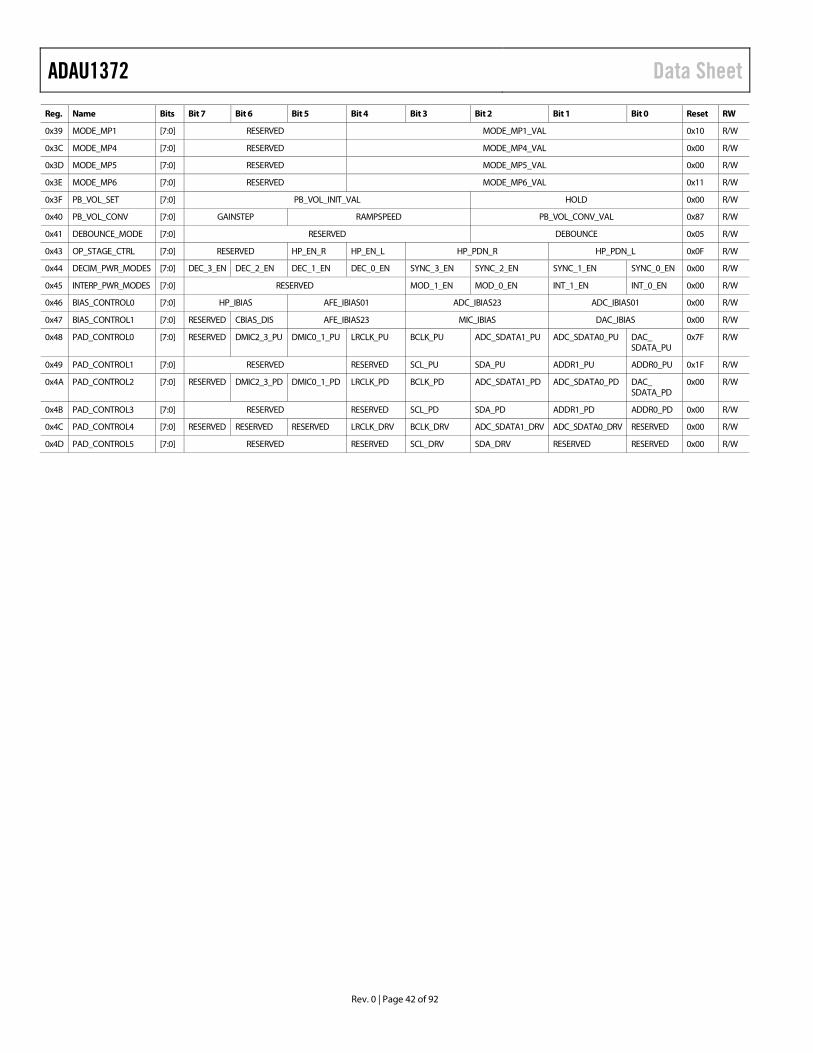
ADAU1372 Data Sheet
Reg. Name Bits Bit 7 Bit 6 Bit 5 Bit 4 Bit 3 Bit 2 Bit 1 Bit 0 Reset RW
0x39 MODE_MP1 [7:0] RESERVED MODE_MP1_VAL 0x10 R/W
0x3C MODE_MP4 [7:0] RESERVED MODE_MP4_VAL 0x00 R/W
0x3D MODE_MP5 [7:0] RESERVED MODE_MP5_VAL 0x00 R/W
0x3E MODE_MP6 [7:0] RESERVED MODE_MP6_VAL 0x11 R/W
0x3F PB_VOL_SET [7:0] PB_VOL_INIT_VAL HOLD 0x00 R/W
0x40 PB_VOL_CONV [7:0] GAINSTEP RAMPSPEED PB_VOL_CONV_VAL 0x87 R/W
0x41 DEBOUNCE_MODE [7:0] RESERVED DEBOUNCE 0x05 R/W
0x43 OP_STAGE_CTRL [7:0] RESERVED HP_EN_R HP_EN_L HP_PDN_R HP_PDN_L 0x0F R/W
0x44 DECIM_PWR_MODES [7:0] DEC_3_EN DEC_2_EN DEC_1_EN DEC_0_EN SYNC_3_EN SYNC_2_EN SYNC_1_EN SYNC_0_EN 0x00 R/W
0x45 INTERP_PWR_MODES [7:0] RESERVED MOD_1_EN MOD_0_EN INT_1_EN INT_0_EN 0x00 R/W
0x46 BIAS_CONTROL0 [7:0] HP_IBIAS AFE_IBIAS01 ADC_IBIAS23 ADC_IBIAS01 0x00 R/W
0x47 BIAS_CONTROL1 [7:0] RESERVED CBIAS_DIS AFE_IBIAS23 MIC_IBIAS DAC_IBIAS 0x00 R/W
0x48 PAD_CONTROL0 [7:0] RESERVED DMIC2_3_PU DMIC0_1_PU LRCLK_PU BCLK_PU ADC_SDATA1_PU ADC_SDATA0_PU DAC_ SDATA_PU
0x7F R/W
0x49 PAD_CONTROL1 [7:0] RESERVED RESERVED SCL_PU SDA_PU ADDR1_PU ADDR0_PU 0x1F R/W
0x4A PAD_CONTROL2 [7:0] RESERVED DMIC2_3_PD DMIC0_1_PD LRCLK_PD BCLK_PD ADC_SDATA1_PD ADC_SDATA0_PD DAC_ SDATA_PD
0x00 R/W
0x4B PAD_CONTROL3 [7:0] RESERVED RESERVED SCL_PD SDA_PD ADDR1_PD ADDR0_PD 0x00 R/W
0x4C PAD_CONTROL4 [7:0] RESERVED RESERVED RESERVED LRCLK_DRV BCLK_DRV ADC_SDATA1_DRV ADC_SDATA0_DRV RESERVED 0x00 R/W
0x4D PAD_CONTROL5 [7:0] RESERVED RESERVED SCL_DRV SDA_DRV RESERVED RESERVED 0x00 R/W
Rev. 0 | Page 42 of 92
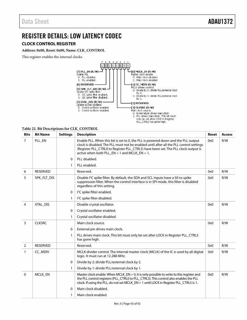
Data Sheet ADAU1372
REGISTER DETAILS: LOW LATENCY CODEC CLOCK CONTROL REGISTER Address: 0x00, Reset: 0x00, Name: CLK_CONTROL
This register enables the internal clocks.
Table 22. Bit Descriptions for CLK_CONTROL Bits Bit Name Settings Description Reset Access
7 PLL_EN Enable PLL. When this bit is set to 0, the PLL is powered down and the PLL output clock is disabled. The PLL must not be enabled until after all the PLL control settings (Register PLL_CTRL0 to Register PLL_CTRL5) have been set. The PLL clock output is active when both PLL_EN = 1 and MCLK_EN = 1.
0x0 R/W
0 PLL disabled.
1 PLL enabled.
6 RESERVED Reserved. 0x0 R/W
5 SPK_FLT_DIS Disable I2C spike filter. By default, the SDA and SCL inputs have a 50 ns spike suppression filter. When the control interface is in SPI mode, this filter is disabled regardless of this setting.
0x0 R/W
0 I2C spike filter enabled.
1 I2C spike filter disabled.
4 XTAL_DIS Disable crystal oscillator. 0x0 R/W
0 Crystal oscillator enabled.
1 Crystal oscillator disabled.
3 CLKSRC Main clock source. 0x0 R/W
0 External pin drives main clock.
1 PLL drives main clock. This bit must only be set after LOCK in Register PLL_CTRL5 has gone high.
2 RESERVED Reserved. 0x0 R/W
1 CC_MDIV MCLK divider control. The internal master clock (MCLK) of the IC is used by all digital logic. It must run at 12.288 MHz.
0x0 R/W
0 Divide by 2: divide PLL/external clock by 2.
1 Divide by 1: divide PLL/external clock by 1.
0 MCLK_EN Master clock enable. When MCLK_EN = 0, it is only possible to write to this register and the PLL control registers (PLL_CTRL0 to PLL_CTRL5). This control also enables the PLL clock. If using the PLL, do not set MCLK_EN = 1 until LOCK in Register PLL_CTRL5 is 1.
0x0 R/W
0 Main clock disabled.
1 Main clock enabled.
Rev. 0 | Page 43 of 92
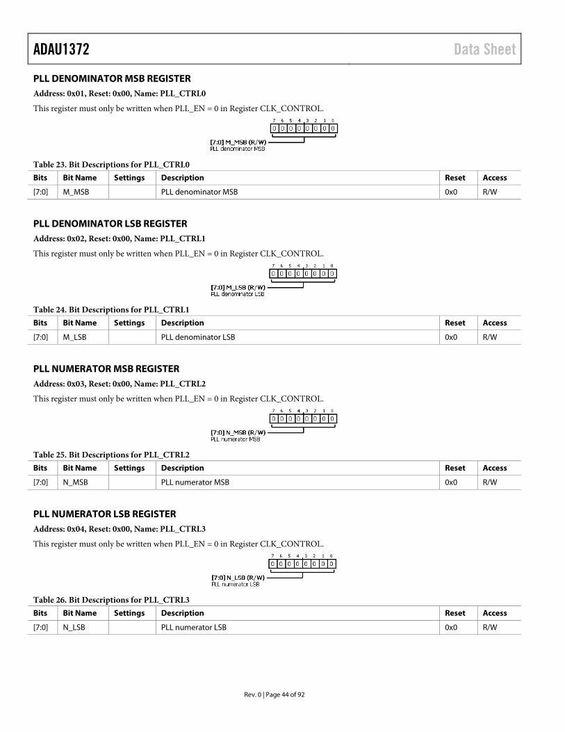
ADAU1372 Data Sheet
PLL DENOMINATOR MSB REGISTER Address: 0x01, Reset: 0x00, Name: PLL_CTRL0
This register must only be written when PLL_EN = 0 in Register CLK_CONTROL.
Table 23. Bit Descriptions for PLL_CTRL0 Bits Bit Name Settings Description Reset Access
[7:0] M_MSB PLL denominator MSB 0x0 R/W
PLL DENOMINATOR LSB REGISTER Address: 0x02, Reset: 0x00, Name: PLL_CTRL1
This register must only be written when PLL_EN = 0 in Register CLK_CONTROL.
Table 24. Bit Descriptions for PLL_CTRL1 Bits Bit Name Settings Description Reset Access
[7:0] M_LSB PLL denominator LSB 0x0 R/W
PLL NUMERATOR MSB REGISTER Address: 0x03, Reset: 0x00, Name: PLL_CTRL2
This register must only be written when PLL_EN = 0 in Register CLK_CONTROL.
Table 25. Bit Descriptions for PLL_CTRL2 Bits Bit Name Settings Description Reset Access
[7:0] N_MSB PLL numerator MSB 0x0 R/W
PLL NUMERATOR LSB REGISTER Address: 0x04, Reset: 0x00, Name: PLL_CTRL3
This register must only be written when PLL_EN = 0 in Register CLK_CONTROL.
Table 26. Bit Descriptions for PLL_CTRL3 Bits Bit Name Settings Description Reset Access
[7:0] N_LSB PLL numerator LSB 0x0 R/W
Rev. 0 | Page 44 of 92
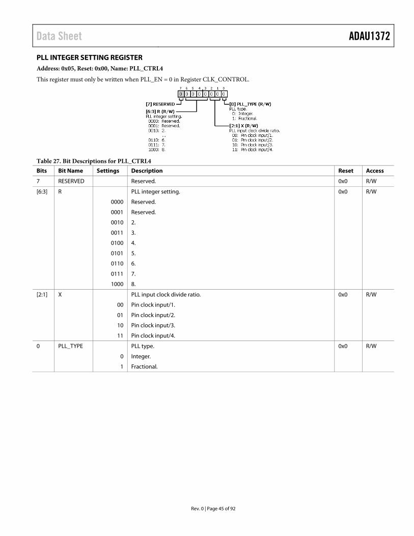
Data Sheet ADAU1372
PLL INTEGER SETTING REGISTER Address: 0x05, Reset: 0x00, Name: PLL_CTRL4
This register must only be written when PLL_EN = 0 in Register CLK_CONTROL.
Table 27. Bit Descriptions for PLL_CTRL4 Bits Bit Name Settings Description Reset Access
7 RESERVED Reserved. 0x0 R/W
[6:3] R PLL integer setting. 0x0 R/W
0000 Reserved.
0001 Reserved.
0010 2.
0011 3.
0100 4.
0101 5.
0110 6.
0111 7.
1000 8.
[2:1] X PLL input clock divide ratio. 0x0 R/W
00 Pin clock input/1.
01 Pin clock input/2.
10 Pin clock input/3.
11 Pin clock input/4.
0 PLL_TYPE PLL type. 0x0 R/W
0 Integer.
1 Fractional.
Rev. 0 | Page 45 of 92
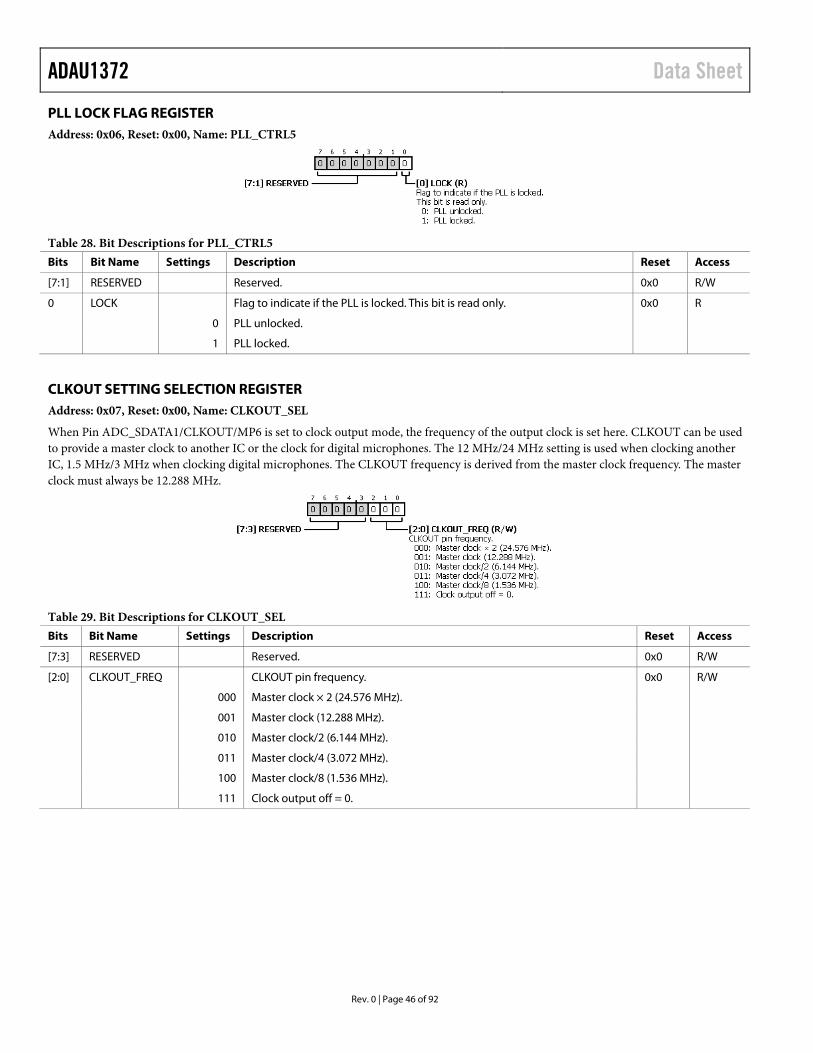
ADAU1372 Data Sheet
PLL LOCK FLAG REGISTER Address: 0x06, Reset: 0x00, Name: PLL_CTRL5
Table 28. Bit Descriptions for PLL_CTRL5 Bits Bit Name Settings Description Reset Access
[7:1] RESERVED Reserved. 0x0 R/W
0 LOCK Flag to indicate if the PLL is locked. This bit is read only. 0x0 R
0 PLL unlocked.
1 PLL locked.
CLKOUT SETTING SELECTION REGISTER Address: 0x07, Reset: 0x00, Name: CLKOUT_SEL
When Pin ADC_SDATA1/CLKOUT/MP6 is set to clock output mode, the frequency of the output clock is set here. CLKOUT can be used to provide a master clock to another IC or the clock for digital microphones. The 12 MHz/24 MHz setting is used when clocking another IC, 1.5 MHz/3 MHz when clocking digital microphones. The CLKOUT frequency is derived from the master clock frequency. The master clock must always be 12.288 MHz.
Table 29. Bit Descriptions for CLKOUT_SEL Bits Bit Name Settings Description Reset Access
[7:3] RESERVED Reserved. 0x0 R/W
[2:0] CLKOUT_FREQ CLKOUT pin frequency. 0x0 R/W
000 Master clock × 2 (24.576 MHz).
001 Master clock (12.288 MHz).
010 Master clock/2 (6.144 MHz).
011 Master clock/4 (3.072 MHz).
100 Master clock/8 (1.536 MHz).
111 Clock output off = 0.
Rev. 0 | Page 46 of 92
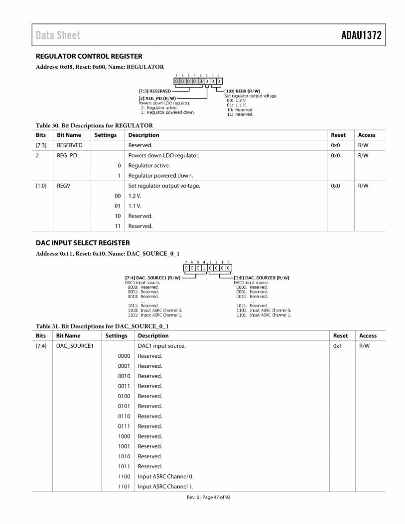
Data Sheet ADAU1372
REGULATOR CONTROL REGISTER Address: 0x08, Reset: 0x00, Name: REGULATOR
Table 30. Bit Descriptions for REGULATOR Bits Bit Name Settings Description Reset Access
[7:3] RESERVED Reserved. 0x0 R/W
2 REG_PD Powers down LDO regulator. 0x0 R/W
0 Regulator active.
1 Regulator powered down.
[1:0] REGV Set regulator output voltage. 0x0 R/W
00 1.2 V.
01 1.1 V.
10 Reserved.
11 Reserved.
DAC INPUT SELECT REGISTER Address: 0x11, Reset: 0x10, Name: DAC_SOURCE_0_1
Table 31. Bit Descriptions for DAC_SOURCE_0_1 Bits Bit Name Settings Description Reset Access
[7:4] DAC_SOURCE1 DAC1 input source. 0x1 R/W
0000 Reserved.
0001 Reserved.
0010 Reserved.
0011 Reserved.
0100 Reserved.
0101 Reserved.
0110 Reserved.
0111 Reserved.
1000 Reserved.
1001 Reserved.
1010 Reserved.
1011 Reserved.
1100 Input ASRC Channel 0.
1101 Input ASRC Channel 1.
Rev. 0 | Page 47 of 92
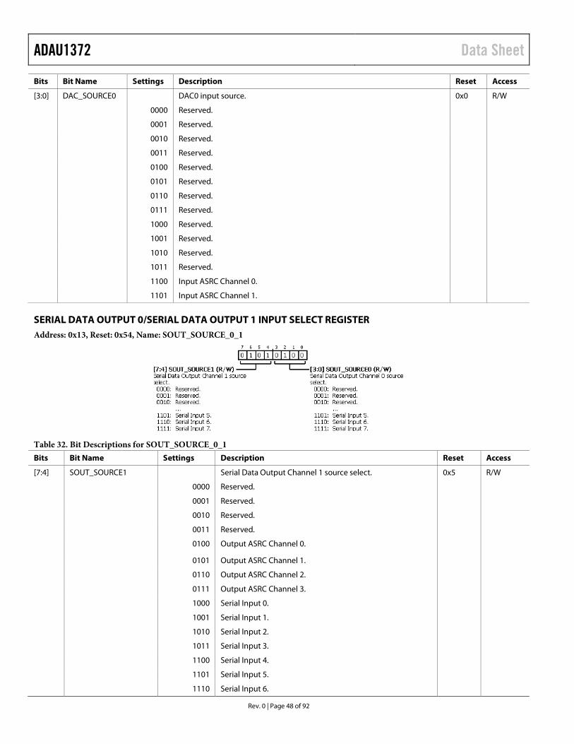
ADAU1372 Data Sheet
Bits Bit Name Settings Description Reset Access
[3:0] DAC_SOURCE0 DAC0 input source. 0x0 R/W
0000 Reserved.
0001 Reserved.
0010 Reserved.
0011 Reserved.
0100 Reserved.
0101 Reserved.
0110 Reserved.
0111 Reserved.
1000 Reserved.
1001 Reserved.
1010 Reserved.
1011 Reserved.
1100 Input ASRC Channel 0.
1101 Input ASRC Channel 1.
SERIAL DATA OUTPUT 0/SERIAL DATA OUTPUT 1 INPUT SELECT REGISTER Address: 0x13, Reset: 0x54, Name: SOUT_SOURCE_0_1
Table 32. Bit Descriptions for SOUT_SOURCE_0_1 Bits Bit Name Settings Description Reset Access
[7:4] SOUT_SOURCE1 Serial Data Output Channel 1 source select. 0x5 R/W
0000 Reserved.
0001 Reserved.
0010 Reserved.
0011 Reserved.
0100 Output ASRC Channel 0.
0101 Output ASRC Channel 1.
0110 Output ASRC Channel 2.
0111 Output ASRC Channel 3.
1000 Serial Input 0.
1001 Serial Input 1.
1010 Serial Input 2.
1011 Serial Input 3.
1100 Serial Input 4.
1101 Serial Input 5.
1110 Serial Input 6.
Rev. 0 | Page 48 of 92
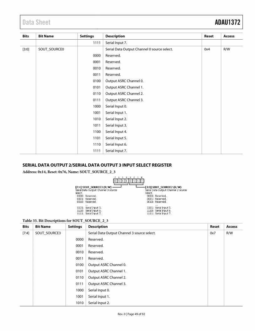
Data Sheet ADAU1372
Bits Bit Name Settings Description Reset Access
1111 Serial Input 7.
[3:0] SOUT_SOURCE0 Serial Data Output Channel 0 source select. 0x4 R/W
0000 Reserved.
0001 Reserved.
0010 Reserved.
0011 Reserved.
0100 Output ASRC Channel 0.
0101 Output ASRC Channel 1.
0110 Output ASRC Channel 2.
0111 Output ASRC Channel 3.
1000 Serial Input 0.
1001 Serial Input 1.
1010 Serial Input 2.
1011 Serial Input 3.
1100 Serial Input 4.
1101 Serial Input 5.
1110 Serial Input 6.
1111 Serial Input 7.
SERIAL DATA OUTPUT 2/SERIAL DATA OUTPUT 3 INPUT SELECT REGISTER Address: 0x14, Reset: 0x76, Name: SOUT_SOURCE_2_3
Table 33. Bit Descriptions for SOUT_SOURCE_2_3 Bits Bit Name Settings Description Reset Access
[7:4] SOUT_SOURCE3 Serial Data Output Channel 3 source select. 0x7 R/W
0000 Reserved.
0001 Reserved.
0010 Reserved.
0011 Reserved.
0100 Output ASRC Channel 0.
0101 Output ASRC Channel 1.
0110 Output ASRC Channel 2.
0111 Output ASRC Channel 3.
1000 Serial Input 0.
1001 Serial Input 1.
1010 Serial Input 2.
Rev. 0 | Page 49 of 92
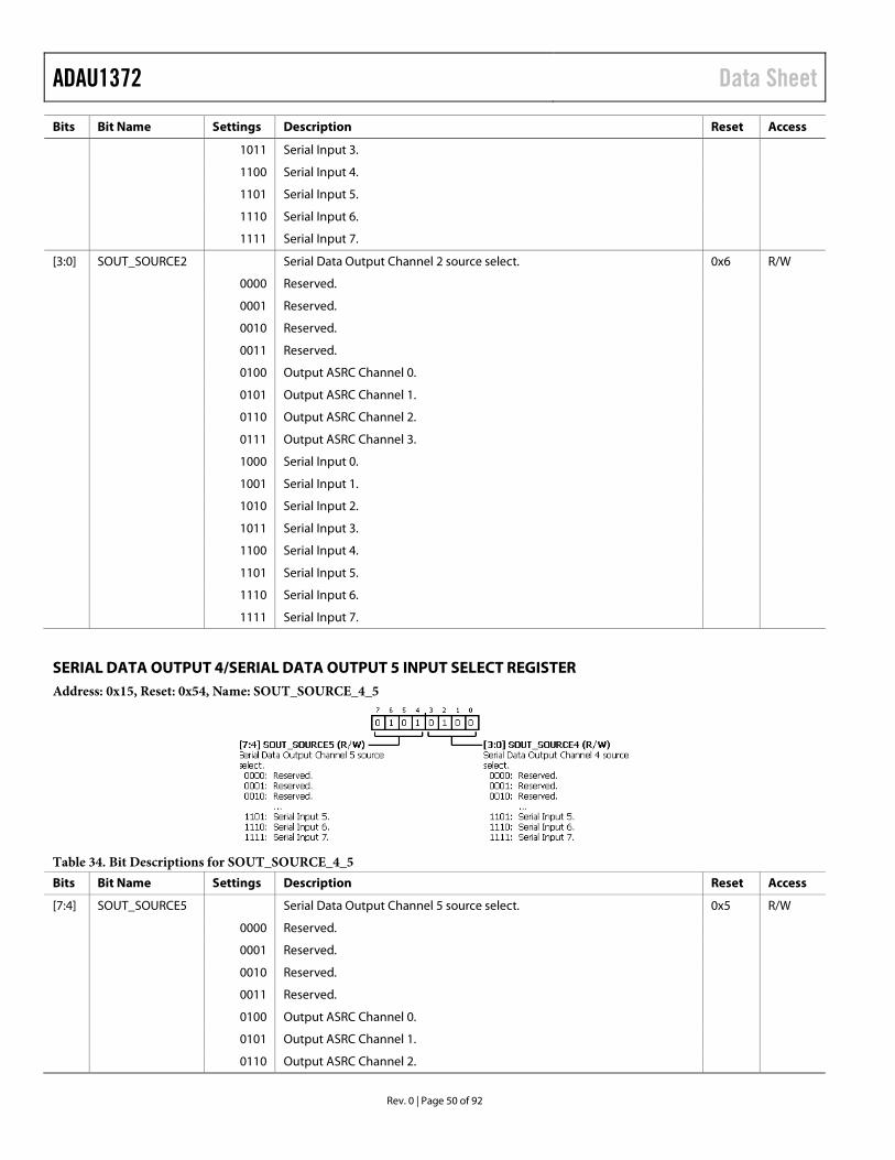
ADAU1372 Data Sheet
Bits Bit Name Settings Description Reset Access
1011 Serial Input 3.
1100 Serial Input 4.
1101 Serial Input 5.
1110 Serial Input 6.
1111 Serial Input 7.
[3:0] SOUT_SOURCE2 Serial Data Output Channel 2 source select. 0x6 R/W
0000 Reserved.
0001 Reserved.
0010 Reserved.
0011 Reserved.
0100 Output ASRC Channel 0.
0101 Output ASRC Channel 1.
0110 Output ASRC Channel 2.
0111 Output ASRC Channel 3.
1000 Serial Input 0.
1001 Serial Input 1.
1010 Serial Input 2.
1011 Serial Input 3.
1100 Serial Input 4.
1101 Serial Input 5.
1110 Serial Input 6.
1111 Serial Input 7.
SERIAL DATA OUTPUT 4/SERIAL DATA OUTPUT 5 INPUT SELECT REGISTER Address: 0x15, Reset: 0x54, Name: SOUT_SOURCE_4_5
Table 34. Bit Descriptions for SOUT_SOURCE_4_5 Bits Bit Name Settings Description Reset Access
[7:4] SOUT_SOURCE5 Serial Data Output Channel 5 source select. 0x5 R/W
0000 Reserved.
0001 Reserved.
0010 Reserved.
0011 Reserved.
0100 Output ASRC Channel 0.
0101 Output ASRC Channel 1.
0110 Output ASRC Channel 2.
Rev. 0 | Page 50 of 92
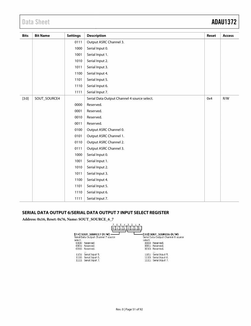
Data Sheet ADAU1372
Bits Bit Name Settings Description Reset Access
0111 Output ASRC Channel 3.
1000 Serial Input 0.
1001 Serial Input 1.
1010 Serial Input 2.
1011 Serial Input 3.
1100 Serial Input 4.
1101 Serial Input 5.
1110 Serial Input 6.
1111 Serial Input 7.
[3:0] SOUT_SOURCE4 Serial Data Output Channel 4 source select. 0x4 R/W
0000 Reserved.
0001 Reserved.
0010 Reserved.
0011 Reserved.
0100 Output ASRC Channel 0.
0101 Output ASRC Channel 1.
0110 Output ASRC Channel 2.
0111 Output ASRC Channel 3.
1000 Serial Input 0.
1001 Serial Input 1.
1010 Serial Input 2.
1011 Serial Input 3.
1100 Serial Input 4.
1101 Serial Input 5.
1110 Serial Input 6.
1111 Serial Input 7.
SERIAL DATA OUTPUT 6/SERIAL DATA OUTPUT 7 INPUT SELECT REGISTER Address: 0x16, Reset: 0x76, Name: SOUT_SOURCE_6_7
Rev. 0 | Page 51 of 92
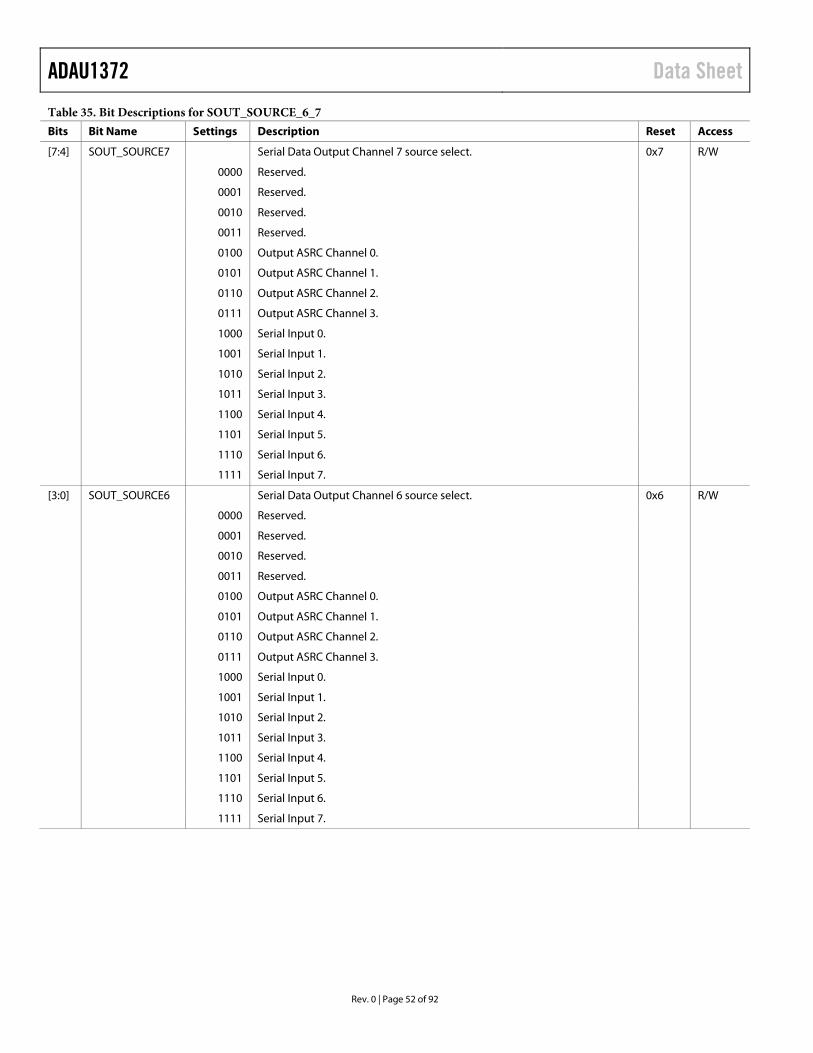
ADAU1372 Data Sheet Table 35. Bit Descriptions for SOUT_SOURCE_6_7 Bits Bit Name Settings Description Reset Access
[7:4] SOUT_SOURCE7 Serial Data Output Channel 7 source select. 0x7 R/W
0000 Reserved.
0001 Reserved.
0010 Reserved.
0011 Reserved.
0100 Output ASRC Channel 0.
0101 Output ASRC Channel 1.
0110 Output ASRC Channel 2.
0111 Output ASRC Channel 3.
1000 Serial Input 0.
1001 Serial Input 1.
1010 Serial Input 2.
1011 Serial Input 3.
1100 Serial Input 4.
1101 Serial Input 5.
1110 Serial Input 6.
1111 Serial Input 7.
[3:0] SOUT_SOURCE6 Serial Data Output Channel 6 source select. 0x6 R/W
0000 Reserved.
0001 Reserved.
0010 Reserved.
0011 Reserved.
0100 Output ASRC Channel 0.
0101 Output ASRC Channel 1.
0110 Output ASRC Channel 2.
0111 Output ASRC Channel 3.
1000 Serial Input 0.
1001 Serial Input 1.
1010 Serial Input 2.
1011 Serial Input 3.
1100 Serial Input 4.
1101 Serial Input 5.
1110 Serial Input 6.
1111 Serial Input 7.
Rev. 0 | Page 52 of 92
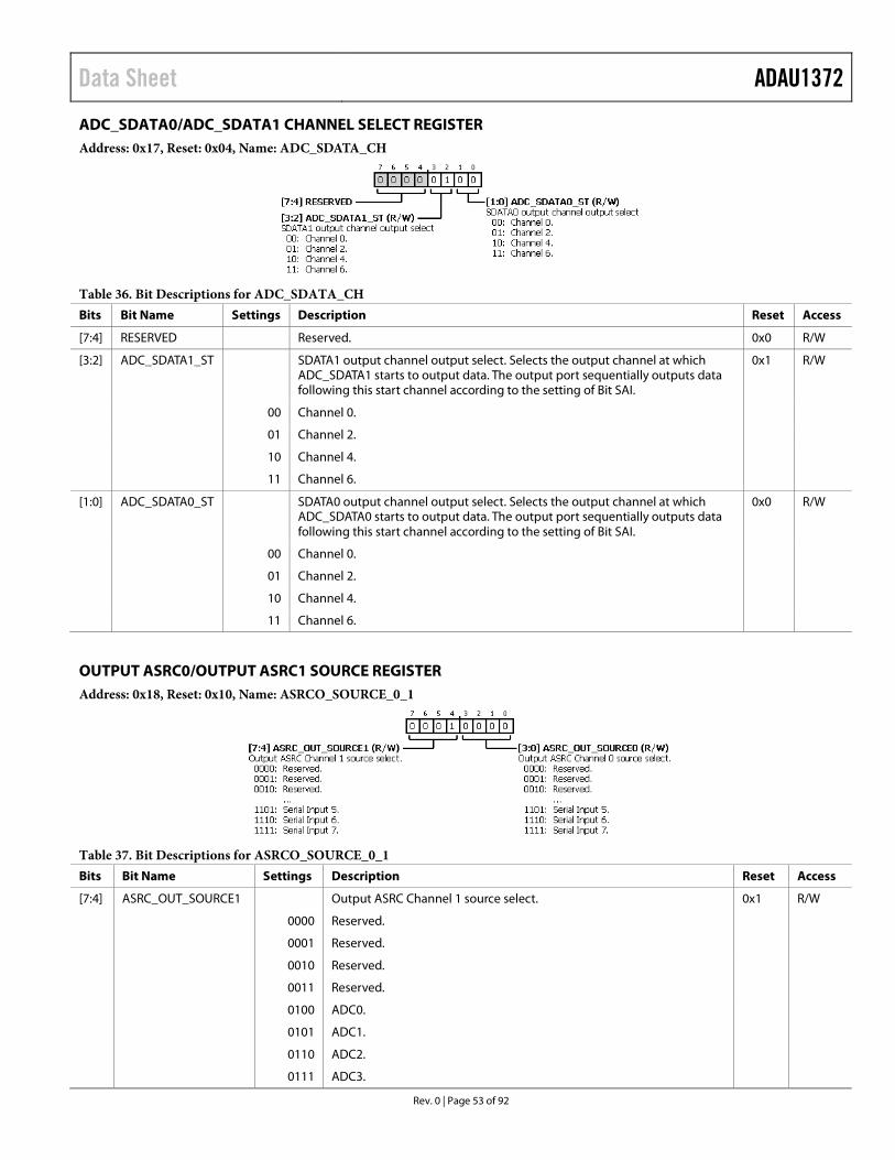
Data Sheet ADAU1372
ADC_SDATA0/ADC_SDATA1 CHANNEL SELECT REGISTER Address: 0x17, Reset: 0x04, Name: ADC_SDATA_CH
Table 36. Bit Descriptions for ADC_SDATA_CH Bits Bit Name Settings Description Reset Access
[7:4] RESERVED Reserved. 0x0 R/W
[3:2] ADC_SDATA1_ST SDATA1 output channel output select. Selects the output channel at which ADC_SDATA1 starts to output data. The output port sequentially outputs data following this start channel according to the setting of Bit SAI.
0x1 R/W
00 Channel 0.
01 Channel 2.
10 Channel 4.
11 Channel 6.
[1:0] ADC_SDATA0_ST SDATA0 output channel output select. Selects the output channel at which ADC_SDATA0 starts to output data. The output port sequentially outputs data following this start channel according to the setting of Bit SAI.
0x0 R/W
00 Channel 0.
01 Channel 2.
10 Channel 4.
11 Channel 6.
OUTPUT ASRC0/OUTPUT ASRC1 SOURCE REGISTER Address: 0x18, Reset: 0x10, Name: ASRCO_SOURCE_0_1
Table 37. Bit Descriptions for ASRCO_SOURCE_0_1 Bits Bit Name Settings Description Reset Access
[7:4] ASRC_OUT_SOURCE1 Output ASRC Channel 1 source select. 0x1 R/W
0000 Reserved.
0001 Reserved.
0010 Reserved.
0011 Reserved.
0100 ADC0.
0101 ADC1.
0110 ADC2.
0111 ADC3.
Rev. 0 | Page 53 of 92
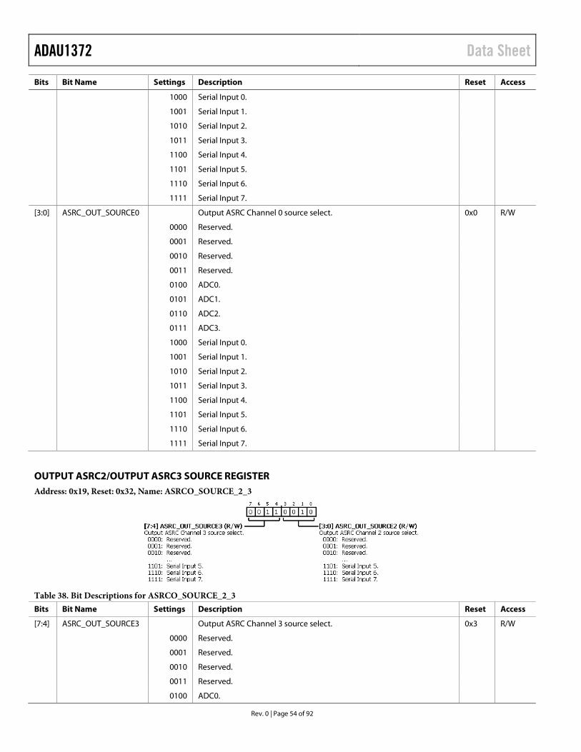
ADAU1372 Data Sheet
Bits Bit Name Settings Description Reset Access
1000 Serial Input 0.
1001 Serial Input 1.
1010 Serial Input 2.
1011 Serial Input 3.
1100 Serial Input 4.
1101 Serial Input 5.
1110 Serial Input 6.
1111 Serial Input 7.
[3:0] ASRC_OUT_SOURCE0 Output ASRC Channel 0 source select. 0x0 R/W
0000 Reserved.
0001 Reserved.
0010 Reserved.
0011 Reserved.
0100 ADC0.
0101 ADC1.
0110 ADC2.
0111 ADC3.
1000 Serial Input 0.
1001 Serial Input 1.
1010 Serial Input 2.
1011 Serial Input 3.
1100 Serial Input 4.
1101 Serial Input 5.
1110 Serial Input 6.
1111 Serial Input 7.
OUTPUT ASRC2/OUTPUT ASRC3 SOURCE REGISTER Address: 0x19, Reset: 0x32, Name: ASRCO_SOURCE_2_3
Table 38. Bit Descriptions for ASRCO_SOURCE_2_3 Bits Bit Name Settings Description Reset Access
[7:4] ASRC_OUT_SOURCE3 Output ASRC Channel 3 source select. 0x3 R/W
0000 Reserved.
0001 Reserved.
0010 Reserved.
0011 Reserved.
0100 ADC0.
Rev. 0 | Page 54 of 92
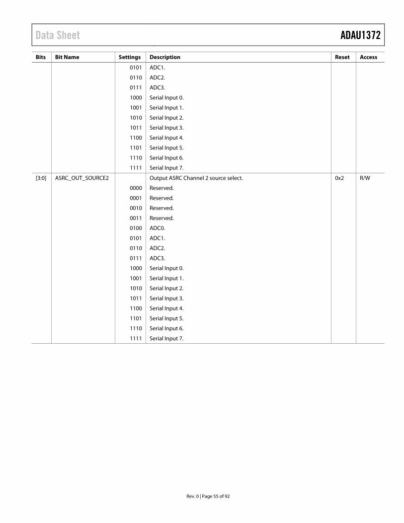
Data Sheet ADAU1372
Bits Bit Name Settings Description Reset Access
0101 ADC1.
0110 ADC2.
0111 ADC3.
1000 Serial Input 0.
1001 Serial Input 1.
1010 Serial Input 2.
1011 Serial Input 3.
1100 Serial Input 4.
1101 Serial Input 5.
1110 Serial Input 6.
1111 Serial Input 7.
[3:0] ASRC_OUT_SOURCE2 Output ASRC Channel 2 source select. 0x2 R/W
0000 Reserved.
0001 Reserved.
0010 Reserved.
0011 Reserved.
0100 ADC0.
0101 ADC1.
0110 ADC2.
0111 ADC3.
1000 Serial Input 0.
1001 Serial Input 1.
1010 Serial Input 2.
1011 Serial Input 3.
1100 Serial Input 4.
1101 Serial Input 5.
1110 Serial Input 6.
1111 Serial Input 7.
Rev. 0 | Page 55 of 92
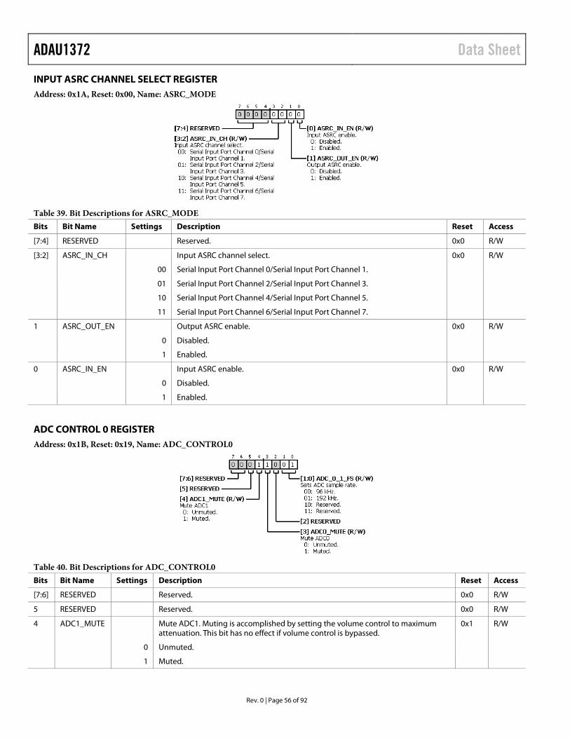
ADAU1372 Data Sheet
INPUT ASRC CHANNEL SELECT REGISTER Address: 0x1A, Reset: 0x00, Name: ASRC_MODE
Table 39. Bit Descriptions for ASRC_MODE Bits Bit Name Settings Description Reset Access
[7:4] RESERVED Reserved. 0x0 R/W
[3:2] ASRC_IN_CH Input ASRC channel select. 0x0 R/W
00 Serial Input Port Channel 0/Serial Input Port Channel 1.
01 Serial Input Port Channel 2/Serial Input Port Channel 3.
10 Serial Input Port Channel 4/Serial Input Port Channel 5.
11 Serial Input Port Channel 6/Serial Input Port Channel 7.
1 ASRC_OUT_EN Output ASRC enable. 0x0 R/W
0 Disabled.
1 Enabled.
0 ASRC_IN_EN Input ASRC enable. 0x0 R/W
0 Disabled.
1 Enabled.
ADC CONTROL 0 REGISTER Address: 0x1B, Reset: 0x19, Name: ADC_CONTROL0
Table 40. Bit Descriptions for ADC_CONTROL0 Bits Bit Name Settings Description Reset Access
[7:6] RESERVED Reserved. 0x0 R/W
5 RESERVED Reserved. 0x0 R/W
4 ADC1_MUTE Mute ADC1. Muting is accomplished by setting the volume control to maximum attenuation. This bit has no effect if volume control is bypassed.
0x1 R/W
0 Unmuted.
1 Muted.
Rev. 0 | Page 56 of 92
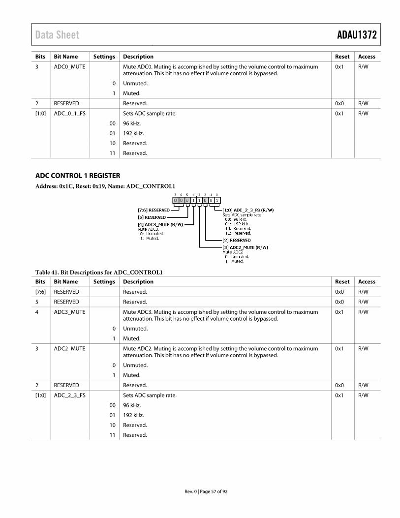
Data Sheet ADAU1372
Bits Bit Name Settings Description Reset Access
3 ADC0_MUTE Mute ADC0. Muting is accomplished by setting the volume control to maximum attenuation. This bit has no effect if volume control is bypassed.
0x1 R/W
0 Unmuted.
1 Muted.
2 RESERVED Reserved. 0x0 R/W
[1:0] ADC_0_1_FS Sets ADC sample rate. 0x1 R/W
00 96 kHz.
01 192 kHz.
10 Reserved.
11 Reserved.
ADC CONTROL 1 REGISTER Address: 0x1C, Reset: 0x19, Name: ADC_CONTROL1
Table 41. Bit Descriptions for ADC_CONTROL1 Bits Bit Name Settings Description Reset Access
[7:6] RESERVED Reserved. 0x0 R/W
5 RESERVED Reserved. 0x0 R/W
4 ADC3_MUTE Mute ADC3. Muting is accomplished by setting the volume control to maximum attenuation. This bit has no effect if volume control is bypassed.
0x1 R/W
0 Unmuted.
1 Muted.
3 ADC2_MUTE Mute ADC2. Muting is accomplished by setting the volume control to maximum attenuation. This bit has no effect if volume control is bypassed.
0x1 R/W
0 Unmuted.
1 Muted.
2 RESERVED Reserved. 0x0 R/W
[1:0] ADC_2_3_FS Sets ADC sample rate. 0x1 R/W
00 96 kHz.
01 192 kHz.
10 Reserved.
11 Reserved.
Rev. 0 | Page 57 of 92
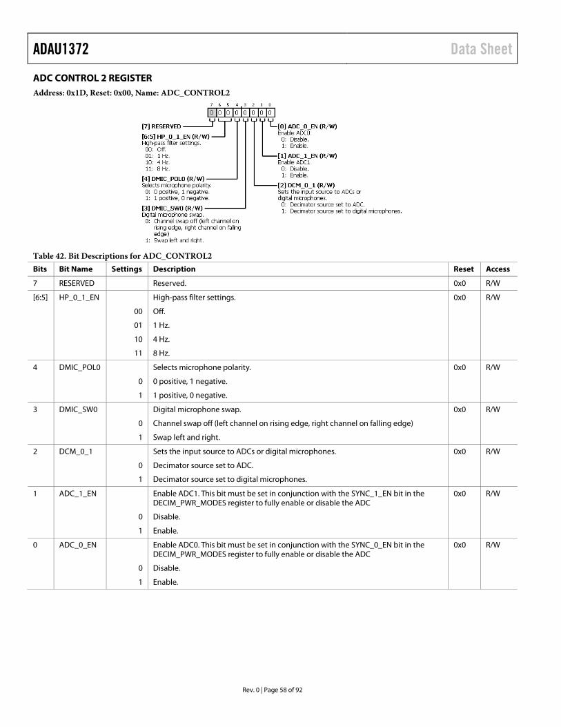
ADAU1372 Data Sheet
ADC CONTROL 2 REGISTER Address: 0x1D, Reset: 0x00, Name: ADC_CONTROL2
Table 42. Bit Descriptions for ADC_CONTROL2 Bits Bit Name Settings Description Reset Access
7 RESERVED Reserved. 0x0 R/W
[6:5] HP_0_1_EN High-pass filter settings. 0x0 R/W
00 Off.
01 1 Hz.
10 4 Hz.
11 8 Hz.
4 DMIC_POL0 Selects microphone polarity. 0x0 R/W
0 0 positive, 1 negative.
1 1 positive, 0 negative.
3 DMIC_SW0 Digital microphone swap. 0x0 R/W
0 Channel swap off (left channel on rising edge, right channel on falling edge)
1 Swap left and right.
2 DCM_0_1 Sets the input source to ADCs or digital microphones. 0x0 R/W
0 Decimator source set to ADC.
1 Decimator source set to digital microphones.
1 ADC_1_EN Enable ADC1. This bit must be set in conjunction with the SYNC_1_EN bit in the DECIM_PWR_MODES register to fully enable or disable the ADC
0x0 R/W
0 Disable.
1 Enable.
0 ADC_0_EN Enable ADC0. This bit must be set in conjunction with the SYNC_0_EN bit in the DECIM_PWR_MODES register to fully enable or disable the ADC
0x0 R/W
0 Disable.
1 Enable.
Rev. 0 | Page 58 of 92
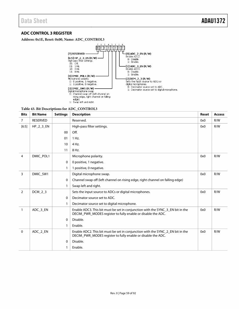
Data Sheet ADAU1372
ADC CONTROL 3 REGISTER Address: 0x1E, Reset: 0x00, Name: ADC_CONTROL3
Table 43. Bit Descriptions for ADC_CONTROL3 Bits Bit Name Settings Description Reset Access
7 RESERVED Reserved. 0x0 R/W
[6:5] HP_2_3_EN High-pass filter settings. 0x0 R/W
00 Off.
01 1 Hz.
10 4 Hz.
11 8 Hz.
4 DMIC_POL1 Microphone polarity. 0x0 R/W
0 0 positive, 1 negative.
1 1 positive, 0 negative.
3 DMIC_SW1 Digital microphone swap. 0x0 R/W
0 Channel swap off (left channel on rising edge, right channel on falling edge)
1 Swap left and right.
2 DCM_2_3 Sets the input source to ADCs or digital microphones. 0x0 R/W
0 Decimator source set to ADC.
1 Decimator source set to digital microphone.
1 ADC_3_EN Enable ADC3. This bit must be set in conjunction with the SYNC_3_EN bit in the DECIM_PWR_MODES register to fully enable or disable the ADC.
0x0 R/W
0 Disable.
1 Enable.
0 ADC_2_EN Enable ADC2. This bit must be set in conjunction with the SYNC_2_EN bit in the DECIM_PWR_MODES register to fully enable or disable the ADC.
0x0 R/W
0 Disable.
1 Enable.
Rev. 0 | Page 59 of 92
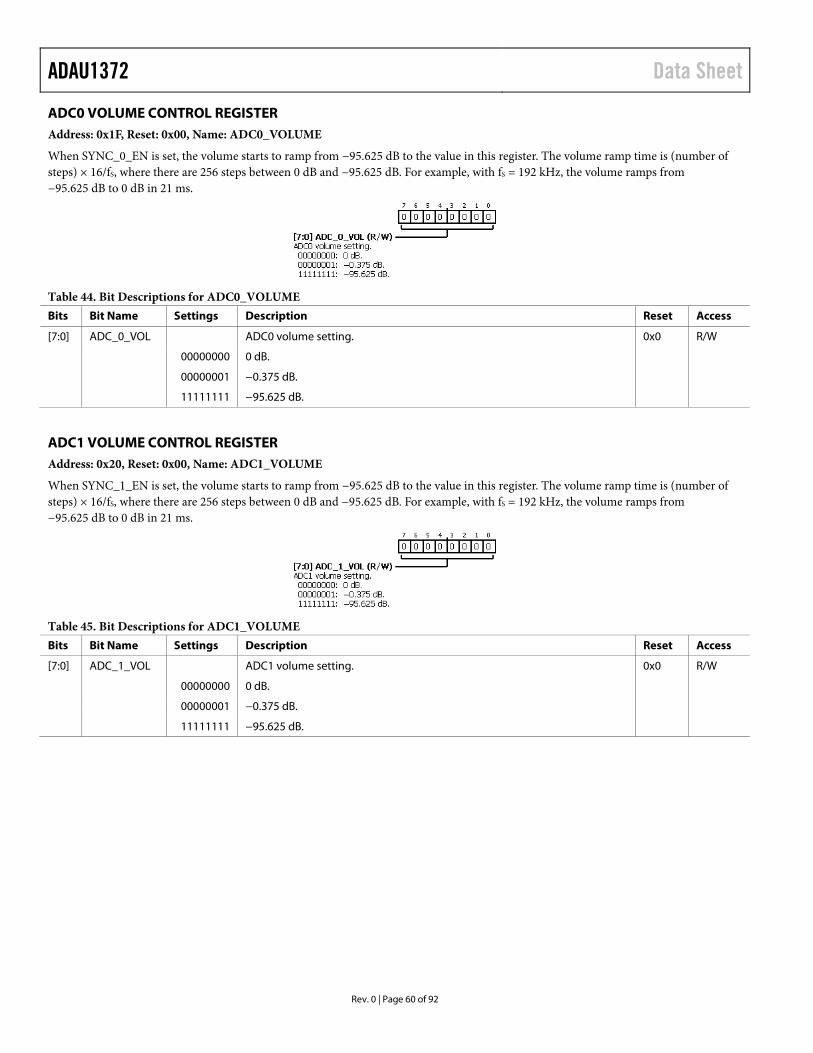
ADAU1372 Data Sheet
ADC0 VOLUME CONTROL REGISTER Address: 0x1F, Reset: 0x00, Name: ADC0_VOLUME
When SYNC_0_EN is set, the volume starts to ramp from −95.625 dB to the value in this register. The volume ramp time is (number of steps) × 16/fS, where there are 256 steps between 0 dB and −95.625 dB. For example, with fS = 192 kHz, the volume ramps from −95.625 dB to 0 dB in 21 ms.
Table 44. Bit Descriptions for ADC0_VOLUME Bits Bit Name Settings Description Reset Access
[7:0] ADC_0_VOL ADC0 volume setting. 0x0 R/W
00000000 0 dB.
00000001 −0.375 dB.
11111111 −95.625 dB.
ADC1 VOLUME CONTROL REGISTER Address: 0x20, Reset: 0x00, Name: ADC1_VOLUME
When SYNC_1_EN is set, the volume starts to ramp from −95.625 dB to the value in this register. The volume ramp time is (number of steps) × 16/fS, where there are 256 steps between 0 dB and −95.625 dB. For example, with fS = 192 kHz, the volume ramps from −95.625 dB to 0 dB in 21 ms.
Table 45. Bit Descriptions for ADC1_VOLUME Bits Bit Name Settings Description Reset Access
[7:0] ADC_1_VOL ADC1 volume setting. 0x0 R/W
00000000 0 dB.
00000001 −0.375 dB.
11111111 −95.625 dB.
Rev. 0 | Page 60 of 92
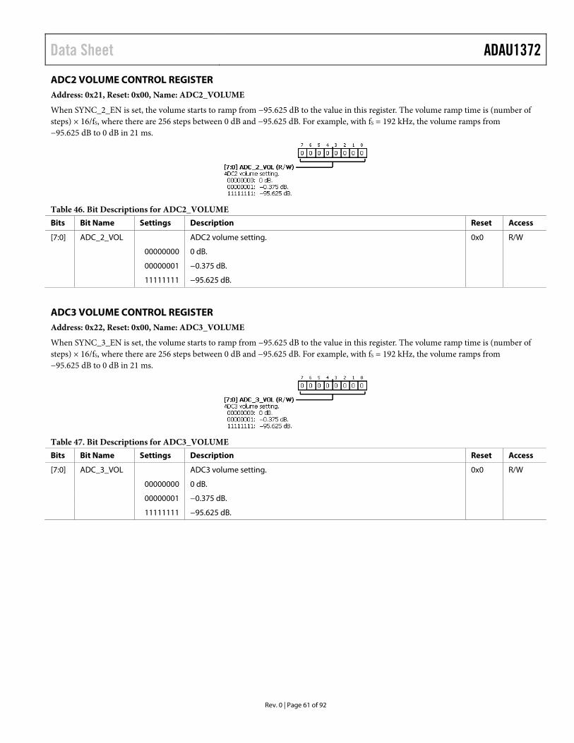
Data Sheet ADAU1372
ADC2 VOLUME CONTROL REGISTER Address: 0x21, Reset: 0x00, Name: ADC2_VOLUME
When SYNC_2_EN is set, the volume starts to ramp from −95.625 dB to the value in this register. The volume ramp time is (number of steps) × 16/fS, where there are 256 steps between 0 dB and −95.625 dB. For example, with fS = 192 kHz, the volume ramps from −95.625 dB to 0 dB in 21 ms.
Table 46. Bit Descriptions for ADC2_VOLUME Bits Bit Name Settings Description Reset Access
[7:0] ADC_2_VOL ADC2 volume setting. 0x0 R/W
00000000 0 dB.
00000001 −0.375 dB.
11111111 −95.625 dB.
ADC3 VOLUME CONTROL REGISTER Address: 0x22, Reset: 0x00, Name: ADC3_VOLUME
When SYNC_3_EN is set, the volume starts to ramp from −95.625 dB to the value in this register. The volume ramp time is (number of steps) × 16/fS, where there are 256 steps between 0 dB and −95.625 dB. For example, with fS = 192 kHz, the volume ramps from −95.625 dB to 0 dB in 21 ms.
Table 47. Bit Descriptions for ADC3_VOLUME Bits Bit Name Settings Description Reset Access
[7:0] ADC_3_VOL ADC3 volume setting. 0x0 R/W
00000000 0 dB.
00000001 −0.375 dB.
11111111 −95.625 dB.
Rev. 0 | Page 61 of 92
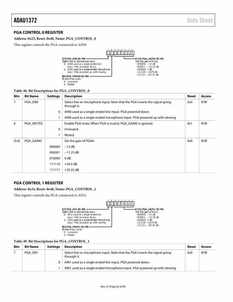
ADAU1372 Data Sheet
PGA CONTROL 0 REGISTER Address: 0x23, Reset: 0x40, Name: PGA_CONTROL_0
This register controls the PGA connected to AIN0.
Table 48. Bit Descriptions for PGA_CONTROL_0 Bits Bit Name Settings Description Reset Access
7 PGA_EN0 Select line or microphone input. Note that the PGA inverts the signal going through it.
0x0 R/W
0 AIN0 used as a single-ended line input. PGA powered down.
1 AIN0 used as a single-ended microphone input. PGA powered up with slewing.
6 PGA_MUTE0 Enable PGA mute. When PGA is muted, PGA_GAIN0 is ignored. 0x1 R/W
0 Unmuted.
1 Muted.
[5:0] PGA_GAIN0 Set the gain of PGA0. 0x0 R/W
000000 −12 dB.
000001 −11.25 dB.
010000 0 dB.
111110 +34.5 dB.
111111 +35.25 dB.
PGA CONTROL 1 REGISTER Address: 0x24, Reset: 0x40, Name: PGA_CONTROL_1
This register controls the PGA connected to AIN1.
Table 49. Bit Descriptions for PGA_CONTROL_1 Bits Bit Name Settings Description Reset Access
7 PGA_EN1 Select line or microphone input. Note that the PGA inverts the signal going through it.
0x0 R/W
0 AIN1 used as a single-ended line input. PGA powered down.
1 AIN1 used as a single-ended microphone input. PGA powered up with slewing.
Rev. 0 | Page 62 of 92
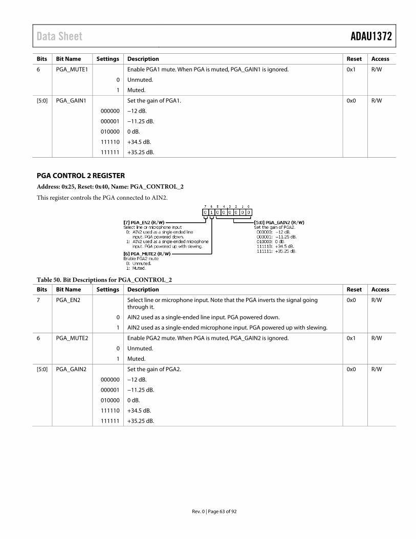
Data Sheet ADAU1372
Bits Bit Name Settings Description Reset Access
6 PGA_MUTE1 Enable PGA1 mute. When PGA is muted, PGA_GAIN1 is ignored. 0x1 R/W
0 Unmuted.
1 Muted.
[5:0] PGA_GAIN1 Set the gain of PGA1. 0x0 R/W
000000 −12 dB.
000001 −11.25 dB.
010000 0 dB.
111110 +34.5 dB.
111111 +35.25 dB.
PGA CONTROL 2 REGISTER Address: 0x25, Reset: 0x40, Name: PGA_CONTROL_2
This register controls the PGA connected to AIN2.
Table 50. Bit Descriptions for PGA_CONTROL_2 Bits Bit Name Settings Description Reset Access
7 PGA_EN2 Select line or microphone input. Note that the PGA inverts the signal going through it.
0x0 R/W
0 AIN2 used as a single-ended line input. PGA powered down.
1 AIN2 used as a single-ended microphone input. PGA powered up with slewing.
6 PGA_MUTE2 Enable PGA2 mute. When PGA is muted, PGA_GAIN2 is ignored. 0x1 R/W
0 Unmuted.
1 Muted.
[5:0] PGA_GAIN2 Set the gain of PGA2. 0x0 R/W
000000 −12 dB.
000001 −11.25 dB.
010000 0 dB.
111110 +34.5 dB.
111111 +35.25 dB.
Rev. 0 | Page 63 of 92
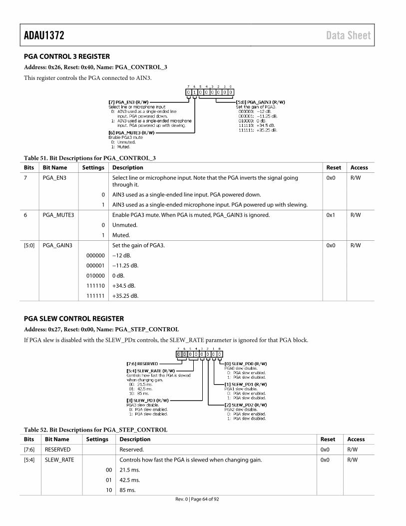
ADAU1372 Data Sheet
PGA CONTROL 3 REGISTER Address: 0x26, Reset: 0x40, Name: PGA_CONTROL_3
This register controls the PGA connected to AIN3.
Table 51. Bit Descriptions for PGA_CONTROL_3 Bits Bit Name Settings Description Reset Access
7 PGA_EN3 Select line or microphone input. Note that the PGA inverts the signal going through it.
0x0 R/W
0 AIN3 used as a single-ended line input. PGA powered down.
1 AIN3 used as a single-ended microphone input. PGA powered up with slewing.
6 PGA_MUTE3 Enable PGA3 mute. When PGA is muted, PGA_GAIN3 is ignored. 0x1 R/W
0 Unmuted.
1 Muted.
[5:0] PGA_GAIN3 Set the gain of PGA3. 0x0 R/W
000000 −12 dB.
000001 −11.25 dB.
010000 0 dB.
111110 +34.5 dB.
111111 +35.25 dB.
PGA SLEW CONTROL REGISTER Address: 0x27, Reset: 0x00, Name: PGA_STEP_CONTROL
If PGA slew is disabled with the SLEW_PDx controls, the SLEW_RATE parameter is ignored for that PGA block.
Table 52. Bit Descriptions for PGA_STEP_CONTROL Bits Bit Name Settings Description Reset Access
[7:6] RESERVED Reserved. 0x0 R/W
[5:4] SLEW_RATE Controls how fast the PGA is slewed when changing gain. 0x0 R/W
00 21.5 ms.
01 42.5 ms.
10 85 ms.
Rev. 0 | Page 64 of 92
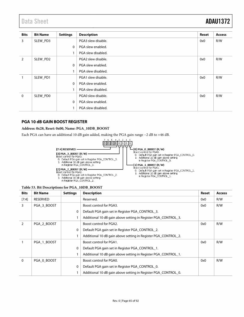
Data Sheet ADAU1372
Bits Bit Name Settings Description Reset Access
3 SLEW_PD3 PGA3 slew disable. 0x0 R/W
0 PGA slew enabled.
1 PGA slew disabled.
2 SLEW_PD2 PGA2 slew disable. 0x0 R/W
0 PGA slew enabled.
1 PGA slew disabled.
1 SLEW_PD1 PGA1 slew disable. 0x0 R/W
0 PGA slew enabled.
1 PGA slew disabled.
0 SLEW_PD0 PGA0 slew disable. 0x0 R/W
0 PGA slew enabled.
1 PGA slew disabled.
PGA 10 dB GAIN BOOST REGISTER
Address: 0x28, Reset: 0x00, Name: PGA_10DB_BOOST
Each PGA can have an additional 10 dB gain added, making the PGA gain range −2 dB to +46 dB.
Table 53. Bit Descriptions for PGA_10DB_BOOST Bits Bit Name Settings Description Reset Access
[7:4] RESERVED Reserved. 0x0 R/W
3 PGA_3_BOOST Boost control for PGA3. 0x0 R/W
0 Default PGA gain set in Register PGA_CONTROL_3.
1 Additional 10 dB gain above setting in Register PGA_CONTROL_3.
2 PGA_2_BOOST Boost control for PGA2. 0x0 R/W
0 Default PGA gain set in Register PGA_CONTROL_2.
1 Additional 10 dB gain above setting in Register PGA_CONTROL_2.
1 PGA_1_BOOST Boost control for PGA1. 0x0 R/W
0 Default PGA gain set in Register PGA_CONTROL_1.
1 Additional 10 dB gain above setting in Register PGA_CONTROL_1.
0 PGA_0_BOOST Boost control for PGA0. 0x0 R/W
0 Default PGA gain set in Register PGA_CONTROL_0.
1 Additional 10 dB gain above setting in Register PGA_CONTROL_0.
Rev. 0 | Page 65 of 92
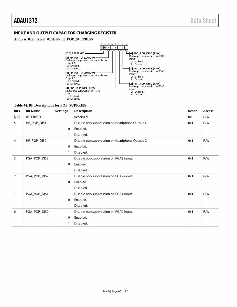
ADAU1372 Data Sheet
INPUT AND OUTPUT CAPACITOR CHARGING REGISTER Address: 0x29, Reset: 0x3F, Name: POP_SUPPRESS
Table 54. Bit Descriptions for POP_SUPPRESS Bits Bit Name Settings Description Reset Access
[7:6] RESERVED Reserved. 0x0 R/W
5 HP_POP_DIS1 Disable pop suppression on Headphone Output 1. 0x1 R/W
0 Enabled.
1 Disabled.
4 HP_POP_DIS0 Disable pop suppression on Headphone Output 0. 0x1 R/W
0 Enabled.
1 Disabled.
3 PGA_POP_DIS3 Disable pop suppression on PGA3 input. 0x1 R/W
0 Enabled.
1 Disabled.
2 PGA_POP_DIS2 Disable pop suppression on PGA2 input. 0x1 R/W
0 Enabled.
1 Disabled.
1 PGA_POP_DIS1 Disable pop suppression on PGA1 input. 0x1 R/W
0 Enabled.
1 Disabled.
0 PGA_POP_DIS0 Disable pop suppression on PGA0 input. 0x1 R/W
0 Enabled.
1 Disabled.
Rev. 0 | Page 66 of 92
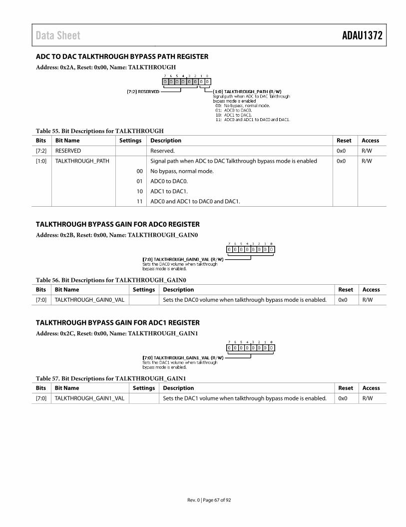
Data Sheet ADAU1372
ADC TO DAC TALKTHROUGH BYPASS PATH REGISTER Address: 0x2A, Reset: 0x00, Name: TALKTHROUGH
Table 55. Bit Descriptions for TALKTHROUGH Bits Bit Name Settings Description Reset Access
[7:2] RESERVED Reserved. 0x0 R/W
[1:0] TALKTHROUGH_PATH Signal path when ADC to DAC Talkthrough bypass mode is enabled 0x0 R/W
00 No bypass, normal mode.
01 ADC0 to DAC0.
10 ADC1 to DAC1.
11 ADC0 and ADC1 to DAC0 and DAC1.
TALKTHROUGH BYPASS GAIN FOR ADC0 REGISTER Address: 0x2B, Reset: 0x00, Name: TALKTHROUGH_GAIN0
Table 56. Bit Descriptions for TALKTHROUGH_GAIN0 Bits Bit Name Settings Description Reset Access
[7:0] TALKTHROUGH_GAIN0_VAL Sets the DAC0 volume when talkthrough bypass mode is enabled. 0x0 R/W
TALKTHROUGH BYPASS GAIN FOR ADC1 REGISTER Address: 0x2C, Reset: 0x00, Name: TALKTHROUGH_GAIN1
Table 57. Bit Descriptions for TALKTHROUGH_GAIN1 Bits Bit Name Settings Description Reset Access
[7:0] TALKTHROUGH_GAIN1_VAL Sets the DAC1 volume when talkthrough bypass mode is enabled. 0x0 R/W
Rev. 0 | Page 67 of 92
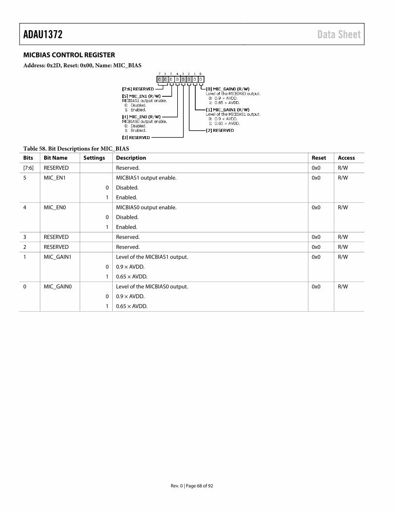
ADAU1372 Data Sheet
MICBIAS CONTROL REGISTER Address: 0x2D, Reset: 0x00, Name: MIC_BIAS
Table 58. Bit Descriptions for MIC_BIAS Bits Bit Name Settings Description Reset Access
[7:6] RESERVED Reserved. 0x0 R/W
5 MIC_EN1 MICBIAS1 output enable. 0x0 R/W
0 Disabled.
1 Enabled.
4 MIC_EN0 MICBIAS0 output enable. 0x0 R/W
0 Disabled.
1 Enabled.
3 RESERVED Reserved. 0x0 R/W
2 RESERVED Reserved. 0x0 R/W
1 MIC_GAIN1 Level of the MICBIAS1 output. 0x0 R/W
0 0.9 × AVDD.
1 0.65 × AVDD.
0 MIC_GAIN0 Level of the MICBIAS0 output. 0x0 R/W
0 0.9 × AVDD.
1 0.65 × AVDD.
Rev. 0 | Page 68 of 92
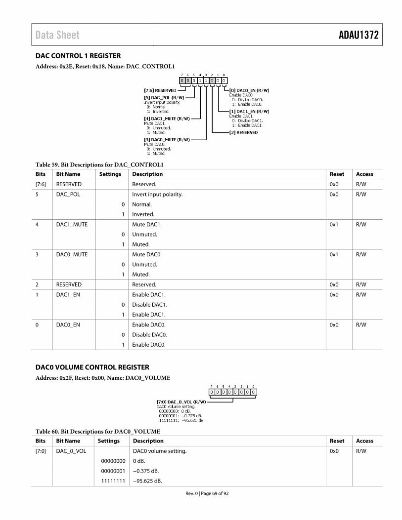
Data Sheet ADAU1372
DAC CONTROL 1 REGISTER Address: 0x2E, Reset: 0x18, Name: DAC_CONTROL1
Table 59. Bit Descriptions for DAC_CONTROL1 Bits Bit Name Settings Description Reset Access
[7:6] RESERVED Reserved. 0x0 R/W
5 DAC_POL Invert input polarity. 0x0 R/W
0 Normal.
1 Inverted.
4 DAC1_MUTE Mute DAC1. 0x1 R/W
0 Unmuted.
1 Muted.
3 DAC0_MUTE Mute DAC0. 0x1 R/W
0 Unmuted.
1 Muted.
2 RESERVED Reserved. 0x0 R/W
1 DAC1_EN Enable DAC1. 0x0 R/W
0 Disable DAC1.
1 Enable DAC1.
0 DAC0_EN Enable DAC0. 0x0 R/W
0 Disable DAC0.
1 Enable DAC0.
DAC0 VOLUME CONTROL REGISTER Address: 0x2F, Reset: 0x00, Name: DAC0_VOLUME
Table 60. Bit Descriptions for DAC0_VOLUME Bits Bit Name Settings Description Reset Access
[7:0] DAC_0_VOL DAC0 volume setting. 0x0 R/W
00000000 0 dB.
00000001 −0.375 dB.
11111111 −95.625 dB.
Rev. 0 | Page 69 of 92
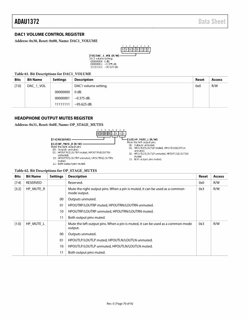
ADAU1372 Data Sheet
DAC1 VOLUME CONTROL REGISTER Address: 0x30, Reset: 0x00, Name: DAC1_VOLUME
Table 61. Bit Descriptions for DAC1_VOLUME Bits Bit Name Settings Description Reset Access
[7:0] DAC_1_VOL DAC1 volume setting. 0x0 R/W
00000000 0 dB.
00000001 −0.375 dB.
11111111 −95.625 dB.
HEADPHONE OUTPUT MUTES REGISTER Address: 0x31, Reset: 0x0F, Name: OP_STAGE_MUTES
Table 62. Bit Descriptions for OP_STAGE_MUTES Bits Bit Name Settings Description Reset Access
[7:4] RESERVED Reserved. 0x0 R/W
[3:2] HP_MUTE_R Mute the right output pins. When a pin is muted, it can be used as a common-mode output.
0x3 R/W
00 Outputs unmuted.
01 HPOUTRP/LOUTRP muted, HPOUTRN/LOUTRN unmuted.
10 HPOUTRP/LOUTRP unmuted, HPOUTRN/LOUTRN muted.
11 Both output pins muted.
[1:0] HP_MUTE_L Mute the left output pins. When a pin is muted, it can be used as a common-mode output.
0x3 R/W
00 Outputs unmuted.
01 HPOUTLP/LOUTLP muted, HPOUTLN/LOUTLN unmuted.
10 HPOUTLP/LOUTLP unmuted, HPOUTLN/LOUTLN muted.
11 Both output pins muted.
Rev. 0 | Page 70 of 92
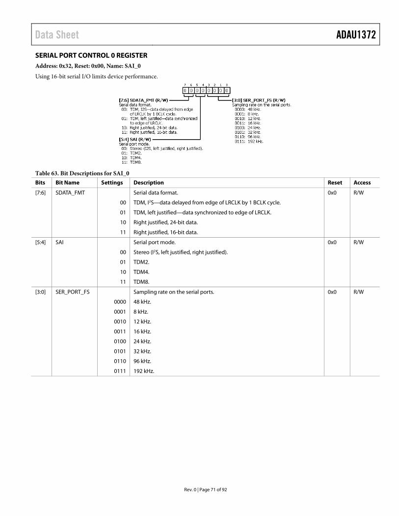
Data Sheet ADAU1372
SERIAL PORT CONTROL 0 REGISTER Address: 0x32, Reset: 0x00, Name: SAI_0
Using 16-bit serial I/O limits device performance.
Table 63. Bit Descriptions for SAI_0 Bits Bit Name Settings Description Reset Access
[7:6] SDATA_FMT Serial data format. 0x0 R/W
00 TDM, I2S—data delayed from edge of LRCLK by 1 BCLK cycle.
01 TDM, left justified—data synchronized to edge of LRCLK.
10 Right justified, 24-bit data.
11 Right justified, 16-bit data.
[5:4] SAI Serial port mode. 0x0 R/W
00 Stereo (I2S, left justified, right justified).
01 TDM2.
10 TDM4.
11 TDM8.
[3:0] SER_PORT_FS Sampling rate on the serial ports. 0x0 R/W
0000 48 kHz.
0001 8 kHz.
0010 12 kHz.
0011 16 kHz.
0100 24 kHz.
0101 32 kHz.
0110 96 kHz.
0111 192 kHz.
Rev. 0 | Page 71 of 92
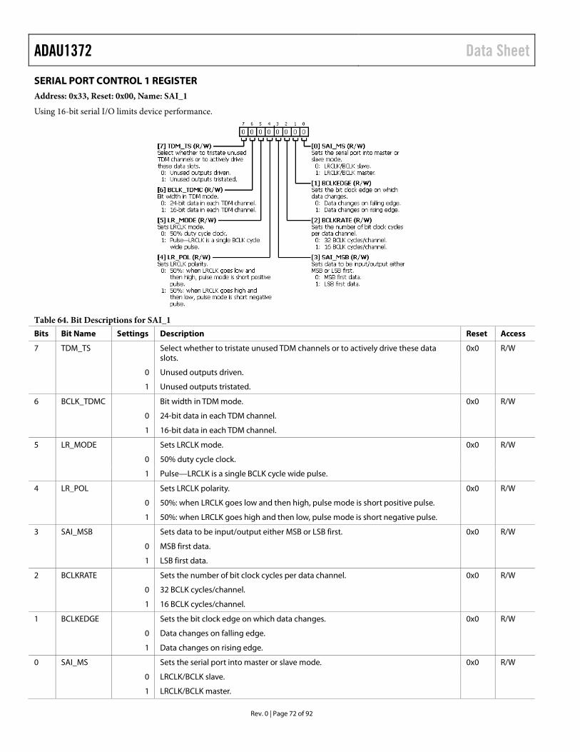
ADAU1372 Data Sheet
SERIAL PORT CONTROL 1 REGISTER Address: 0x33, Reset: 0x00, Name: SAI_1
Using 16-bit serial I/O limits device performance.
Table 64. Bit Descriptions for SAI_1 Bits Bit Name Settings Description Reset Access
7 TDM_TS Select whether to tristate unused TDM channels or to actively drive these data slots.
0x0 R/W
0 Unused outputs driven.
1 Unused outputs tristated.
6 BCLK_TDMC Bit width in TDM mode. 0x0 R/W
0 24-bit data in each TDM channel.
1 16-bit data in each TDM channel.
5 LR_MODE Sets LRCLK mode. 0x0 R/W
0 50% duty cycle clock.
1 Pulse—LRCLK is a single BCLK cycle wide pulse.
4 LR_POL Sets LRCLK polarity. 0x0 R/W
0 50%: when LRCLK goes low and then high, pulse mode is short positive pulse.
1 50%: when LRCLK goes high and then low, pulse mode is short negative pulse.
3 SAI_MSB Sets data to be input/output either MSB or LSB first. 0x0 R/W
0 MSB first data.
1 LSB first data.
2 BCLKRATE Sets the number of bit clock cycles per data channel. 0x0 R/W
0 32 BCLK cycles/channel.
1 16 BCLK cycles/channel.
1 BCLKEDGE Sets the bit clock edge on which data changes. 0x0 R/W
0 Data changes on falling edge.
1 Data changes on rising edge.
0 SAI_MS Sets the serial port into master or slave mode. 0x0 R/W
0 LRCLK/BCLK slave.
1 LRCLK/BCLK master.
Rev. 0 | Page 72 of 92
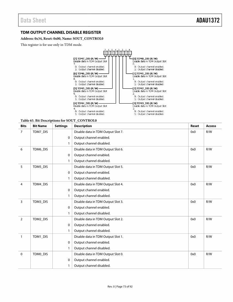
Data Sheet ADAU1372
TDM OUTPUT CHANNEL DISABLE REGISTER Address: 0x34, Reset: 0x00, Name: SOUT_CONTROL0
This register is for use only in TDM mode.
Table 65. Bit Descriptions for SOUT_CONTROL0 Bits Bit Name Settings Description Reset Access
7 TDM7_DIS Disable data in TDM Output Slot 7. 0x0 R/W
0 Output channel enabled.
1 Output channel disabled.
6 TDM6_DIS Disable data in TDM Output Slot 6. 0x0 R/W
0 Output channel enabled.
1 Output channel disabled.
5 TDM5_DIS Disable data in TDM Output Slot 5. 0x0 R/W
0 Output channel enabled.
1 Output channel disabled.
4 TDM4_DIS Disable data in TDM Output Slot 4. 0x0 R/W
0 Output channel enabled.
1 Output channel disabled.
3 TDM3_DIS Disable data in TDM Output Slot 3. 0x0 R/W
0 Output channel enabled.
1 Output channel disabled.
2 TDM2_DIS Disable data in TDM Output Slot 2. 0x0 R/W
0 Output channel enabled.
1 Output channel disabled.
1 TDM1_DIS Disable data in TDM Output Slot 1. 0x0 R/W
0 Output channel enabled.
1 Output channel disabled.
0 TDM0_DIS Disable data in TDM Output Slot 0. 0x0 R/W
0 Output channel enabled.
1 Output channel disabled.
Rev. 0 | Page 73 of 92
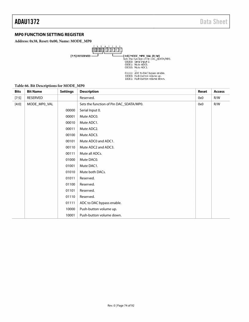
ADAU1372 Data Sheet
MP0 FUNCTION SETTING REGISTER Address: 0x38, Reset: 0x00, Name: MODE_MP0
Table 66. Bit Descriptions for MODE_MP0 Bits Bit Name Settings Description Reset Access
[7:5] RESERVED Reserved. 0x0 R/W
[4:0] MODE_MP0_VAL Sets the function of Pin DAC_SDATA/MP0. 0x0 R/W
00000 Serial Input 0.
00001 Mute ADC0.
00010 Mute ADC1.
00011 Mute ADC2.
00100 Mute ADC3.
00101 Mute ADC0 and ADC1.
00110 Mute ADC2 and ADC3.
00111 Mute all ADCs.
01000 Mute DAC0.
01001 Mute DAC1.
01010 Mute both DACs.
01011 Reserved.
01100 Reserved.
01101 Reserved.
01110 Reserved.
01111 ADC to DAC bypass enable.
10000 Push-button volume up.
10001 Push-button volume down.
Rev. 0 | Page 74 of 92
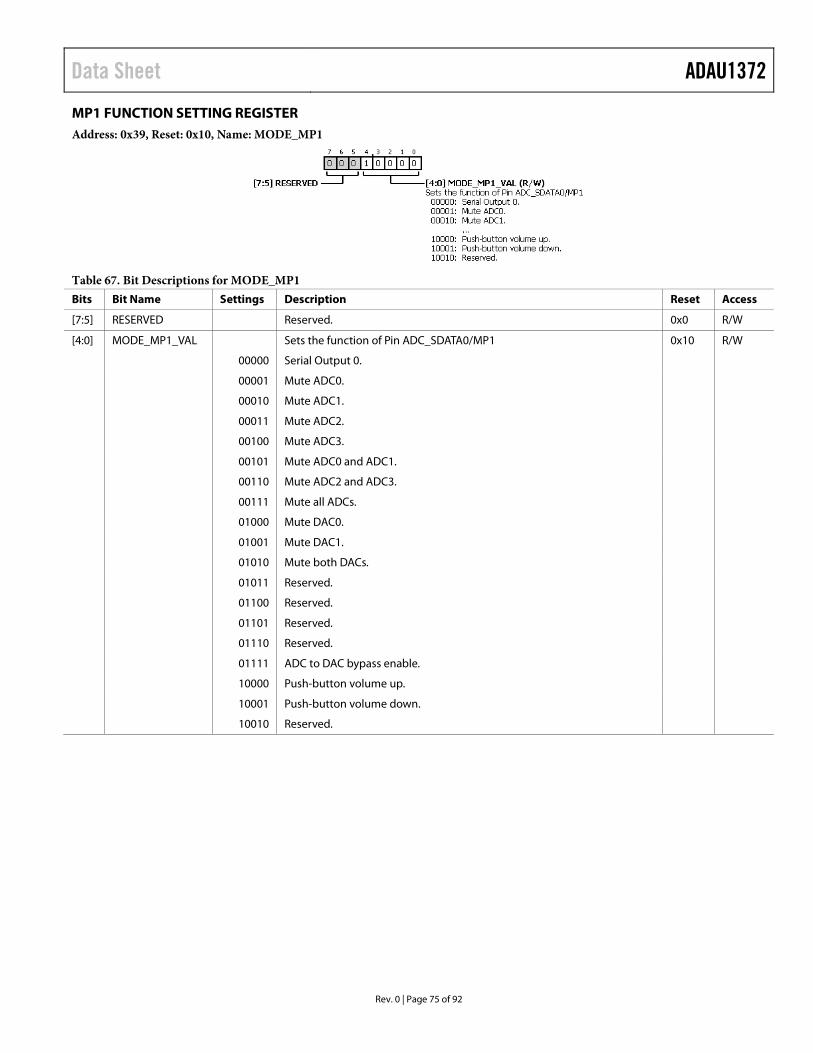
Data Sheet ADAU1372
MP1 FUNCTION SETTING REGISTER Address: 0x39, Reset: 0x10, Name: MODE_MP1
Table 67. Bit Descriptions for MODE_MP1 Bits Bit Name Settings Description Reset Access
[7:5] RESERVED Reserved. 0x0 R/W
[4:0] MODE_MP1_VAL Sets the function of Pin ADC_SDATA0/MP1 0x10 R/W
00000 Serial Output 0.
00001 Mute ADC0.
00010 Mute ADC1.
00011 Mute ADC2.
00100 Mute ADC3.
00101 Mute ADC0 and ADC1.
00110 Mute ADC2 and ADC3.
00111 Mute all ADCs.
01000 Mute DAC0.
01001 Mute DAC1.
01010 Mute both DACs.
01011 Reserved.
01100 Reserved.
01101 Reserved.
01110 Reserved.
01111 ADC to DAC bypass enable.
10000 Push-button volume up.
10001 Push-button volume down.
10010 Reserved.
Rev. 0 | Page 75 of 92
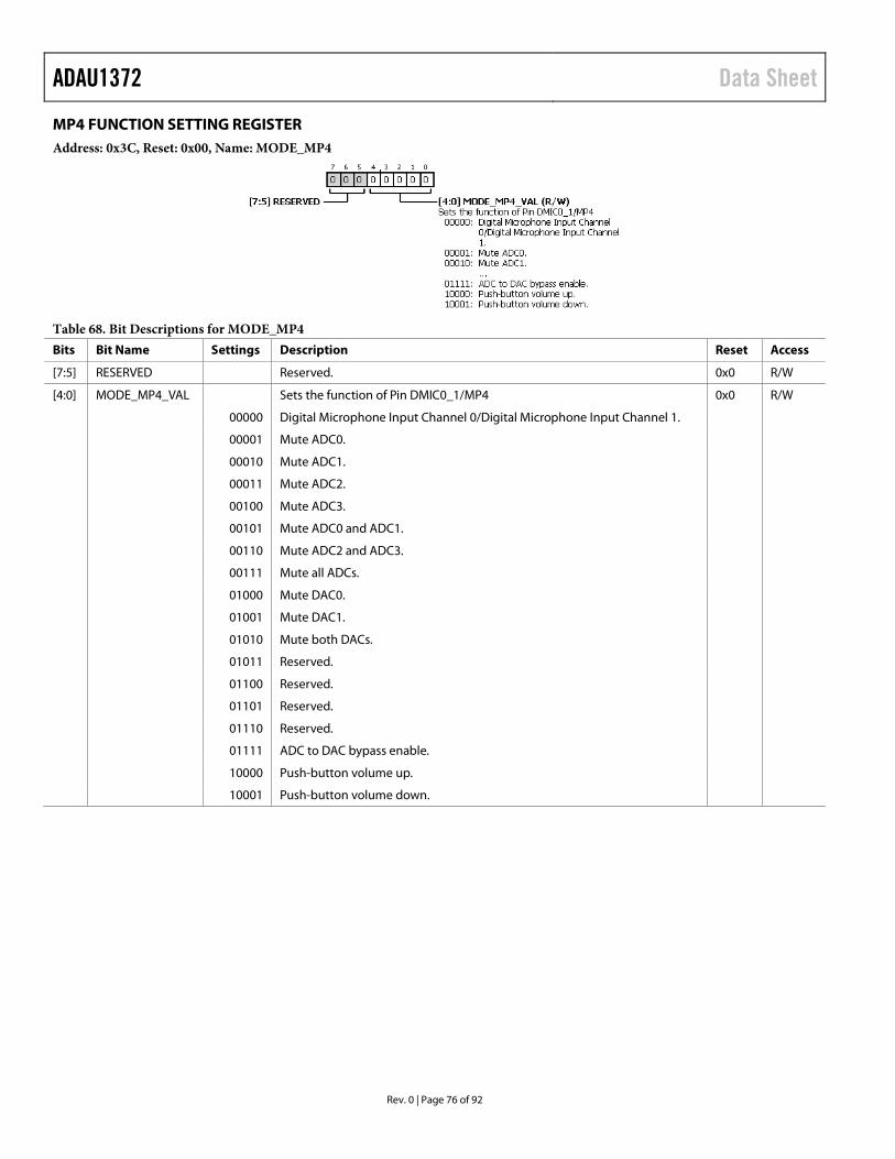
ADAU1372 Data Sheet
MP4 FUNCTION SETTING REGISTER Address: 0x3C, Reset: 0x00, Name: MODE_MP4
Table 68. Bit Descriptions for MODE_MP4 Bits Bit Name Settings Description Reset Access
[7:5] RESERVED Reserved. 0x0 R/W
[4:0] MODE_MP4_VAL Sets the function of Pin DMIC0_1/MP4 0x0 R/W
00000 Digital Microphone Input Channel 0/Digital Microphone Input Channel 1.
00001 Mute ADC0.
00010 Mute ADC1.
00011 Mute ADC2.
00100 Mute ADC3.
00101 Mute ADC0 and ADC1.
00110 Mute ADC2 and ADC3.
00111 Mute all ADCs.
01000 Mute DAC0.
01001 Mute DAC1.
01010 Mute both DACs.
01011 Reserved.
01100 Reserved.
01101 Reserved.
01110 Reserved.
01111 ADC to DAC bypass enable.
10000 Push-button volume up.
10001 Push-button volume down.
Rev. 0 | Page 76 of 92
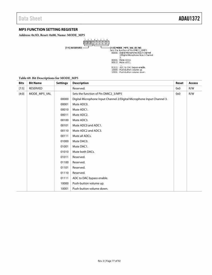
Data Sheet ADAU1372
MP5 FUNCTION SETTING REGISTER Address: 0x3D, Reset: 0x00, Name: MODE_MP5
Table 69. Bit Descriptions for MODE_MP5 Bits Bit Name Settings Description Reset Access
[7:5] RESERVED Reserved. 0x0 R/W
[4:0] MODE_MP5_VAL Sets the function of Pin DMIC2_3/MP5 0x0 R/W
00000 Digital Microphone Input Channel 2/Digital Microphone Input Channel 3.
00001 Mute ADC0.
00010 Mute ADC1.
00011 Mute ADC2.
00100 Mute ADC3.
00101 Mute ADC0 and ADC1.
00110 Mute ADC2 and ADC3.
00111 Mute all ADCs.
01000 Mute DAC0.
01001 Mute DAC1.
01010 Mute both DACs.
01011 Reserved.
01100 Reserved.
01101 Reserved.
01110 Reserved.
01111 ADC to DAC bypass enable.
10000 Push-button volume up.
10001 Push-button volume down.
Rev. 0 | Page 77 of 92
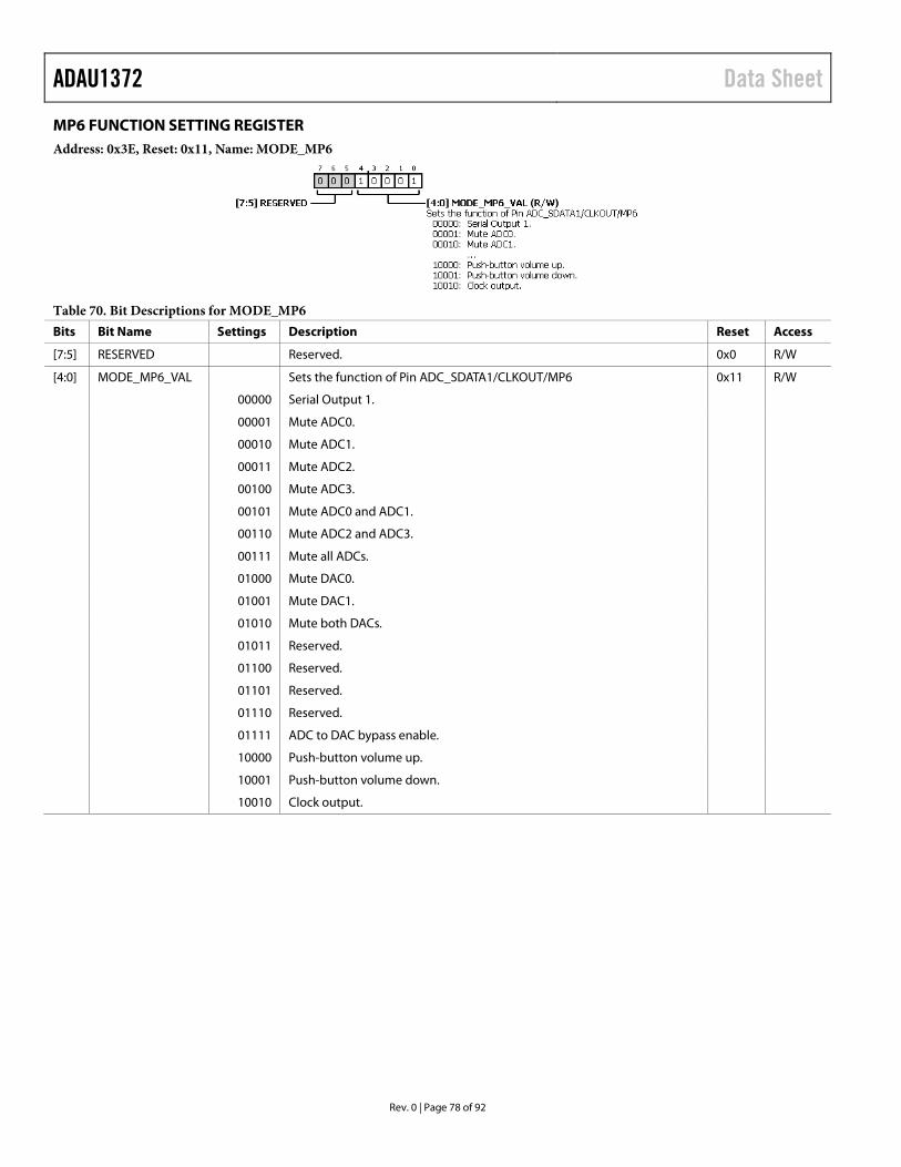
ADAU1372 Data Sheet
MP6 FUNCTION SETTING REGISTER Address: 0x3E, Reset: 0x11, Name: MODE_MP6
Table 70. Bit Descriptions for MODE_MP6 Bits Bit Name Settings Description Reset Access
[7:5] RESERVED Reserved. 0x0 R/W
[4:0] MODE_MP6_VAL Sets the function of Pin ADC_SDATA1/CLKOUT/MP6 0x11 R/W
00000 Serial Output 1.
00001 Mute ADC0.
00010 Mute ADC1.
00011 Mute ADC2.
00100 Mute ADC3.
00101 Mute ADC0 and ADC1.
00110 Mute ADC2 and ADC3.
00111 Mute all ADCs.
01000 Mute DAC0.
01001 Mute DAC1.
01010 Mute both DACs.
01011 Reserved.
01100 Reserved.
01101 Reserved.
01110 Reserved.
01111 ADC to DAC bypass enable.
10000 Push-button volume up.
10001 Push-button volume down.
10010 Clock output.
Rev. 0 | Page 78 of 92
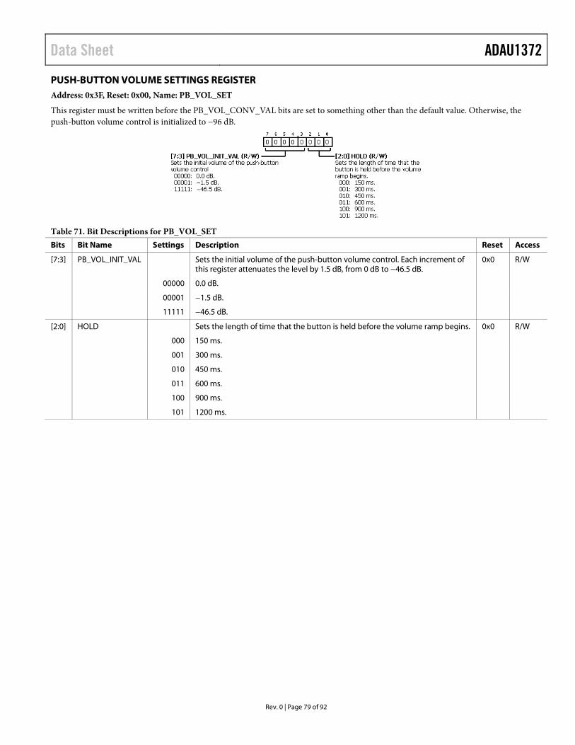
Data Sheet ADAU1372
PUSH-BUTTON VOLUME SETTINGS REGISTER Address: 0x3F, Reset: 0x00, Name: PB_VOL_SET
This register must be written before the PB_VOL_CONV_VAL bits are set to something other than the default value. Otherwise, the push-button volume control is initialized to −96 dB.
Table 71. Bit Descriptions for PB_VOL_SET Bits Bit Name Settings Description Reset Access
[7:3] PB_VOL_INIT_VAL Sets the initial volume of the push-button volume control. Each increment of this register attenuates the level by 1.5 dB, from 0 dB to −46.5 dB.
0x0 R/W
00000 0.0 dB.
00001 −1.5 dB.
11111 −46.5 dB.
[2:0] HOLD Sets the length of time that the button is held before the volume ramp begins. 0x0 R/W
000 150 ms.
001 300 ms.
010 450 ms.
011 600 ms.
100 900 ms.
101 1200 ms.
Rev. 0 | Page 79 of 92
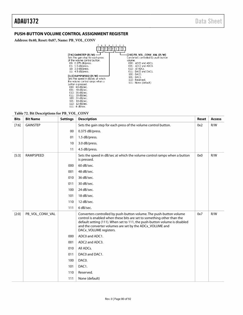
ADAU1372 Data Sheet
PUSH-BUTTON VOLUME CONTROL ASSIGNMENT REGISTER Address: 0x40, Reset: 0x87, Name: PB_VOL_CONV
Table 72. Bit Descriptions for PB_VOL_CONV Bits Bit Name Settings Description Reset Access
[7:6] GAINSTEP Sets the gain step for each press of the volume control button. 0x2 R/W
00 0.375 dB/press.
01 1.5 dB/press.
10 3.0 dB/press.
11 4.5 dB/press.
[5:3] RAMPSPEED Sets the speed in dB/sec at which the volume control ramps when a button is pressed.
0x0 R/W
000 60 dB/sec.
001 48 dB/sec.
010 36 dB/sec.
011 30 dB/sec.
100 24 dB/sec.
101 18 dB/sec.
110 12 dB/sec.
111 6 dB/sec.
[2:0] PB_VOL_CONV_VAL Converters controlled by push-button volume. The push-button volume control is enabled when these bits are set to something other than the default setting (111). When set to 111, the push-button volume is disabled and the converter volumes are set by the ADCx_VOLUME and DACx_VOLUME registers.
0x7 R/W
000 ADC0 and ADC1.
001 ADC2 and ADC3.
010 All ADCs.
011 DAC0 and DAC1.
100 DAC0.
101 DAC1.
110 Reserved.
111 None (default)
Rev. 0 | Page 80 of 92
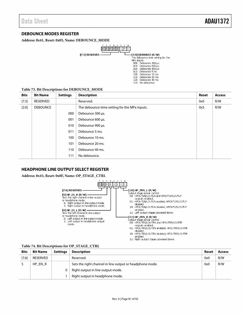
Data Sheet ADAU1372
DEBOUNCE MODES REGISTER Address: 0x41, Reset: 0x05, Name: DEBOUNCE_MODE
Table 73. Bit Descriptions for DEBOUNCE_MODE Bits Bit Name Settings Description Reset Access
[7:3] RESERVED Reserved. 0x0 R/W
[2:0] DEBOUNCE The debounce time setting for the MPx inputs. 0x5 R/W
000 Debounce 300 µs.
001 Debounce 600 µs.
010 Debounce 900 µs.
011 Debounce 5 ms.
100 Debounce 10 ms.
101 Debounce 20 ms.
110 Debounce 40 ms.
111 No debounce.
HEADPHONE LINE OUTPUT SELECT REGISTER Address: 0x43, Reset: 0x0F, Name: OP_STAGE_CTRL
Table 74. Bit Descriptions for OP_STAGE_CTRL Bits Bit Name Settings Description Reset Access
[7:6] RESERVED Reserved. 0x0 R/W
5 HP_EN_R Sets the right channel in line output or headphone mode. 0x0 R/W
0 Right output in line output mode.
1 Right output in headphone mode.
Rev. 0 | Page 81 of 92
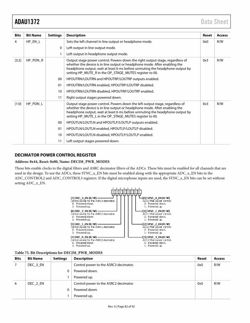
ADAU1372 Data Sheet
Bits Bit Name Settings Description Reset Access
4 HP_EN_L Sets the left channel in line output or headphone mode. 0x0 R/W
0 Left output in line output mode.
1 Left output in headphone output mode.
[3:2] HP_PDN_R Output stage power control. Powers down the right output stage, regardless of whether the device is in line output or headphone mode. After enabling the headphone output, wait at least 6 ms before unmuting the headphone output by setting HP_MUTE_R in the OP_STAGE_MUTES register to 00.
0x3 R/W
00 HPOUTRN/LOUTRN and HPOUTRP/LOUTRP outputs enabled.
01 HPOUTRN/LOUTRN enabled, HPOUTRP/LOUTRP disabled.
10 HPOUTRN/LOUTRN disabled, HPOUTRP/LOUTRP enabled.
11 Right output stages powered down.
[1:0] HP_PDN_L Output stage power control. Powers down the left output stage, regardless of whether the device is in line output or headphone mode. After enabling the headphone output, wait at least 6 ms before unmuting the headphone output by setting HP_MUTE_L in the OP_STAGE_MUTES register to 00.
0x3 R/W
00 HPOUTLN/LOUTLN and HPOUTLP/LOUTLP outputs enabled.
01 HPOUTLN/LOUTLN enabled, HPOUTLP/LOUTLP disabled.
10 HPOUTLN/LOUTLN disabled, HPOUTLP/LOUTLP enabled.
11 Left output stages powered down.
DECIMATOR POWER CONTROL REGISTER Address: 0x44, Reset: 0x00, Name: DECIM_PWR_MODES
These bits enable clocks to the digital filters and ASRC decimator filters of the ADCs. These bits must be enabled for all channels that are used in the design. To use the ADCs, these SYNC_x_EN bits must be enabled along with the appropriate ADC_x_EN bits in the ADC_CONTROL2 and ADC_CONTROL3 registers. If the digital microphone inputs are used, the SYNC_x_EN bits can be set without setting ADC_x_EN.
Table 75. Bit Descriptions for DECIM_PWR_MODES Bits Bit Name Settings Description Reset Access
7 DEC_3_EN Control power to the ASRC3 decimator. 0x0 R/W
0 Powered down.
1 Powered up.
6 DEC_2_EN Control power to the ASRC2 decimator. 0x0 R/W
0 Powered down.
1 Powered up.
Rev. 0 | Page 82 of 92
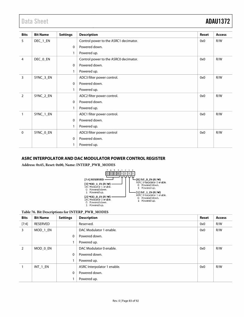
Data Sheet ADAU1372
Bits Bit Name Settings Description Reset Access
5 DEC_1_EN Control power to the ASRC1 decimator. 0x0 R/W
0 Powered down.
1 Powered up.
4 DEC_0_EN Control power to the ASRC0 decimator. 0x0 R/W
0 Powered down.
1 Powered up.
3 SYNC_3_EN ADC3 filter power control. 0x0 R/W
0 Powered down.
1 Powered up.
2 SYNC_2_EN ADC2 filter power control. 0x0 R/W
0 Powered down.
1 Powered up.
1 SYNC_1_EN ADC1 filter power control. 0x0 R/W
0 Powered down.
1 Powered up.
0 SYNC_0_EN ADC0 filter power control 0x0 R/W
0 Powered down.
1 Powered up.
ASRC INTERPOLATOR AND DAC MODULATOR POWER CONTROL REGISTER Address: 0x45, Reset: 0x00, Name: INTERP_PWR_MODES
Table 76. Bit Descriptions for INTERP_PWR_MODES Bits Bit Name Settings Description Reset Access
[7:4] RESERVED Reserved. 0x0 R/W
3 MOD_1_EN DAC Modulator 1 enable. 0x0 R/W
0 Powered down.
1 Powered up.
2 MOD_0_EN DAC Modulator 0 enable. 0x0 R/W
0 Powered down.
1 Powered up.
1 INT_1_EN ASRC Interpolator 1 enable. 0x0 R/W
0 Powered down.
1 Powered up.
Rev. 0 | Page 83 of 92
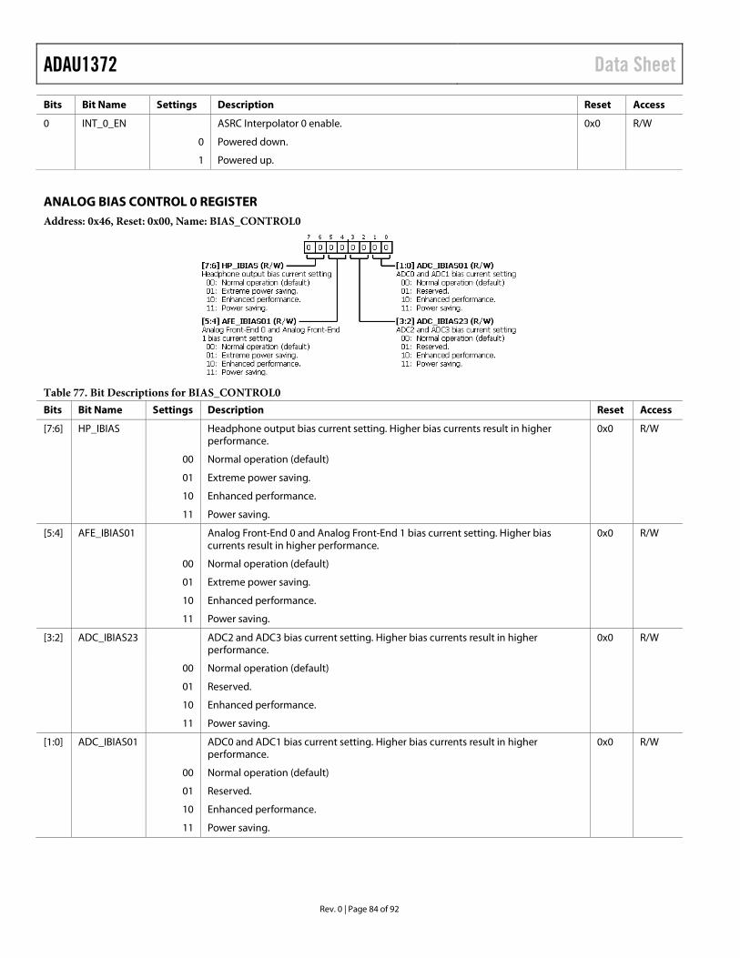
ADAU1372 Data Sheet
Bits Bit Name Settings Description Reset Access
0 INT_0_EN ASRC Interpolator 0 enable. 0x0 R/W
0 Powered down.
1 Powered up.
ANALOG BIAS CONTROL 0 REGISTER Address: 0x46, Reset: 0x00, Name: BIAS_CONTROL0
Table 77. Bit Descriptions for BIAS_CONTROL0 Bits Bit Name Settings Description Reset Access
[7:6] HP_IBIAS Headphone output bias current setting. Higher bias currents result in higher performance.
0x0 R/W
00 Normal operation (default)
01 Extreme power saving.
10 Enhanced performance.
11 Power saving.
[5:4] AFE_IBIAS01 Analog Front-End 0 and Analog Front-End 1 bias current setting. Higher bias currents result in higher performance.
0x0 R/W
00 Normal operation (default)
01 Extreme power saving.
10 Enhanced performance.
11 Power saving.
[3:2] ADC_IBIAS23 ADC2 and ADC3 bias current setting. Higher bias currents result in higher performance.
0x0 R/W
00 Normal operation (default)
01 Reserved.
10 Enhanced performance.
11 Power saving.
[1:0] ADC_IBIAS01 ADC0 and ADC1 bias current setting. Higher bias currents result in higher performance.
0x0 R/W
00 Normal operation (default)
01 Reserved.
10 Enhanced performance.
11 Power saving.
Rev. 0 | Page 84 of 92
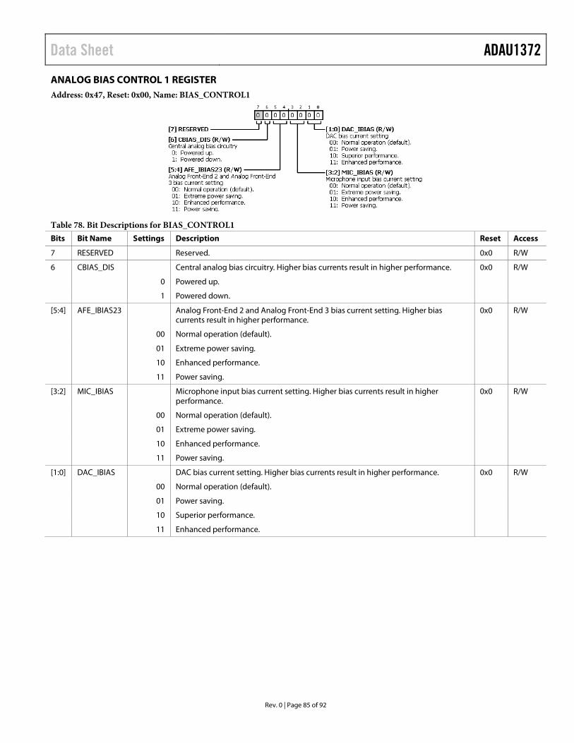
Data Sheet ADAU1372
ANALOG BIAS CONTROL 1 REGISTER Address: 0x47, Reset: 0x00, Name: BIAS_CONTROL1
Table 78. Bit Descriptions for BIAS_CONTROL1 Bits Bit Name Settings Description Reset Access
7 RESERVED Reserved. 0x0 R/W
6 CBIAS_DIS Central analog bias circuitry. Higher bias currents result in higher performance. 0x0 R/W
0 Powered up.
1 Powered down.
[5:4] AFE_IBIAS23 Analog Front-End 2 and Analog Front-End 3 bias current setting. Higher bias currents result in higher performance.
0x0 R/W
00 Normal operation (default).
01 Extreme power saving.
10 Enhanced performance.
11 Power saving.
[3:2] MIC_IBIAS Microphone input bias current setting. Higher bias currents result in higher performance.
0x0 R/W
00 Normal operation (default).
01 Extreme power saving.
10 Enhanced performance.
11 Power saving.
[1:0] DAC_IBIAS DAC bias current setting. Higher bias currents result in higher performance. 0x0 R/W
00 Normal operation (default).
01 Power saving.
10 Superior performance.
11 Enhanced performance.
Rev. 0 | Page 85 of 92
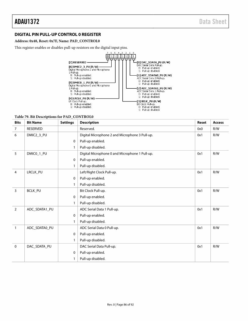
ADAU1372 Data Sheet
DIGITAL PIN PULL-UP CONTROL 0 REGISTER Address: 0x48, Reset: 0x7F, Name: PAD_CONTROL0
This register enables or disables pull-up resistors on the digital input pins.
Table 79. Bit Descriptions for PAD_CONTROL0 Bits Bit Name Settings Description Reset Access
7 RESERVED Reserved. 0x0 R/W
6 DMIC2_3_PU Digital Microphone 2 and Microphone 3 Pull-up. 0x1 R/W
0 Pull-up enabled.
1 Pull-up disabled.
5 DMIC0_1_PU Digital Microphone 0 and Microphone 1 Pull-up. 0x1 R/W
0 Pull-up enabled.
1 Pull-up disabled.
4 LRCLK_PU Left/Right Clock Pull-up. 0x1 R/W
0 Pull-up enabled.
1 Pull-up disabled.
3 BCLK_PU Bit Clock Pull-up. 0x1 R/W
0 Pull-up enabled.
1 Pull-up disabled.
2 ADC_SDATA1_PU ADC Serial Data 1 Pull-up. 0x1 R/W
0 Pull-up enabled.
1 Pull-up disabled.
1 ADC_SDATA0_PU ADC Serial Data 0 Pull-up. 0x1 R/W
0 Pull-up enabled.
1 Pull-up disabled.
0 DAC_SDATA_PU DAC Serial Data Pull-up. 0x1 R/W
0 Pull-up enabled.
1 Pull-up disabled.
Rev. 0 | Page 86 of 92
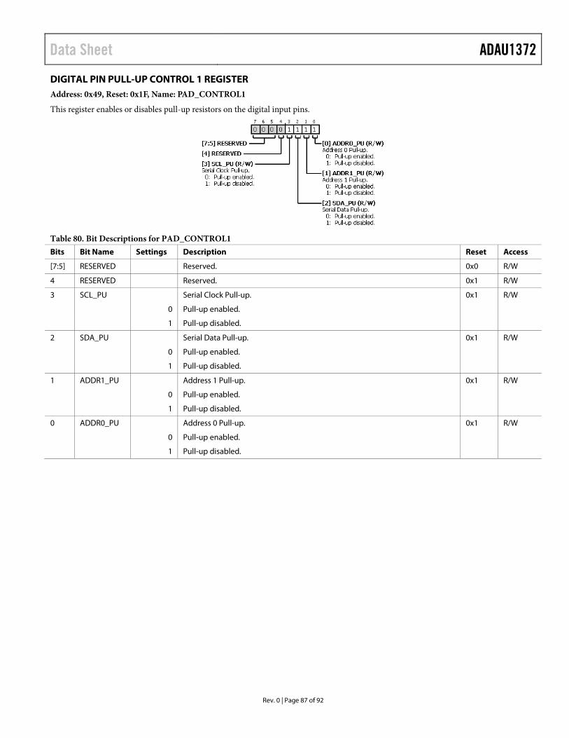
Data Sheet ADAU1372
DIGITAL PIN PULL-UP CONTROL 1 REGISTER Address: 0x49, Reset: 0x1F, Name: PAD_CONTROL1
This register enables or disables pull-up resistors on the digital input pins.
Table 80. Bit Descriptions for PAD_CONTROL1 Bits Bit Name Settings Description Reset Access
[7:5] RESERVED Reserved. 0x0 R/W
4 RESERVED Reserved. 0x1 R/W
3 SCL_PU Serial Clock Pull-up. 0x1 R/W
0 Pull-up enabled.
1 Pull-up disabled.
2 SDA_PU Serial Data Pull-up. 0x1 R/W
0 Pull-up enabled.
1 Pull-up disabled.
1 ADDR1_PU Address 1 Pull-up. 0x1 R/W
0 Pull-up enabled.
1 Pull-up disabled.
0 ADDR0_PU Address 0 Pull-up. 0x1 R/W
0 Pull-up enabled.
1 Pull-up disabled.
Rev. 0 | Page 87 of 92
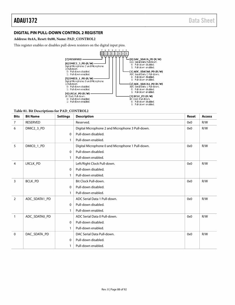
ADAU1372 Data Sheet
DIGITAL PIN PULL-DOWN CONTROL 2 REGISTER Address: 0x4A, Reset: 0x00, Name: PAD_CONTROL2
This register enables or disables pull-down resistors on the digital input pins.
Table 81. Bit Descriptions for PAD_CONTROL2 Bits Bit Name Settings Description Reset Access
7 RESERVED Reserved. 0x0 R/W
6 DMIC2_3_PD Digital Microphone 2 and Microphone 3 Pull-down. 0x0 R/W
0 Pull-down disabled.
1 Pull-down enabled.
5 DMIC0_1_PD Digital Microphone 0 and Microphone 1 Pull-down. 0x0 R/W
0 Pull-down disabled.
1 Pull-down enabled.
4 LRCLK_PD Left/Right Clock Pull-down. 0x0 R/W
0 Pull-down disabled.
1 Pull-down enabled.
3 BCLK_PD Bit Clock Pull-down. 0x0 R/W
0 Pull-down disabled.
1 Pull-down enabled.
2 ADC_SDATA1_PD ADC Serial Data 1 Pull-down. 0x0 R/W
0 Pull-down disabled.
1 Pull-down enabled.
1 ADC_SDATA0_PD ADC Serial Data 0 Pull-down. 0x0 R/W
0 Pull-down disabled.
1 Pull-down enabled.
0 DAC_SDATA_PD DAC Serial Data Pull-down. 0x0 R/W
0 Pull-down disabled.
1 Pull-down enabled.
Rev. 0 | Page 88 of 92
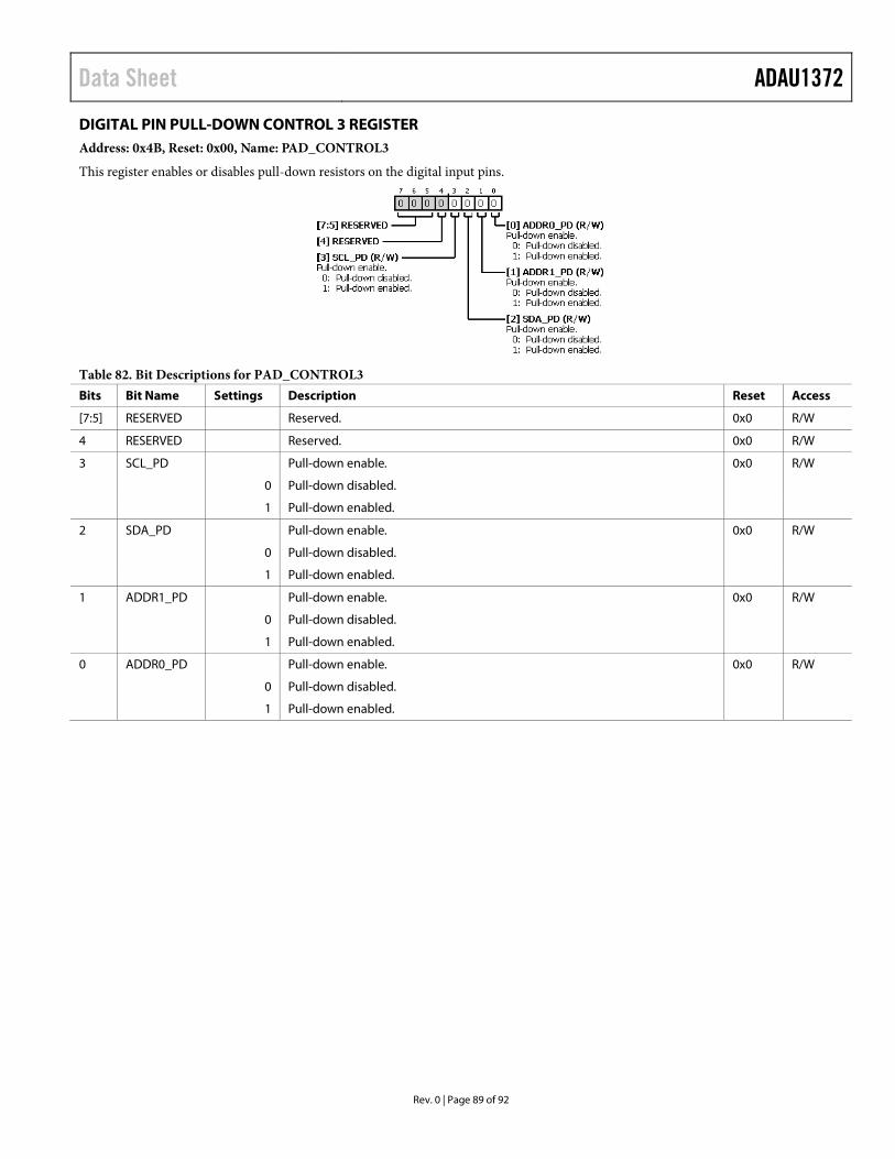
Data Sheet ADAU1372
DIGITAL PIN PULL-DOWN CONTROL 3 REGISTER Address: 0x4B, Reset: 0x00, Name: PAD_CONTROL3
This register enables or disables pull-down resistors on the digital input pins.
Table 82. Bit Descriptions for PAD_CONTROL3 Bits Bit Name Settings Description Reset Access
[7:5] RESERVED Reserved. 0x0 R/W
4 RESERVED Reserved. 0x0 R/W
3 SCL_PD Pull-down enable. 0x0 R/W
0 Pull-down disabled.
1 Pull-down enabled.
2 SDA_PD Pull-down enable. 0x0 R/W
0 Pull-down disabled.
1 Pull-down enabled.
1 ADDR1_PD Pull-down enable. 0x0 R/W
0 Pull-down disabled.
1 Pull-down enabled.
0 ADDR0_PD Pull-down enable. 0x0 R/W
0 Pull-down disabled.
1 Pull-down enabled.
Rev. 0 | Page 89 of 92
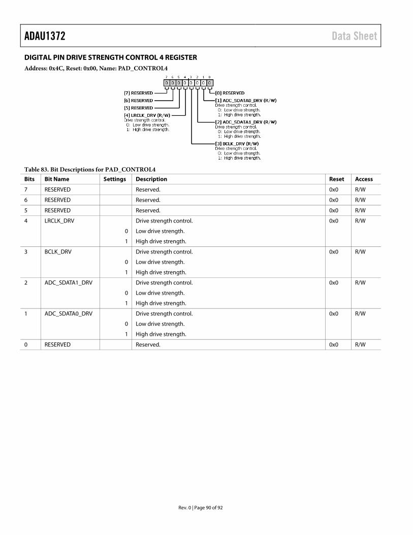
ADAU1372 Data Sheet
DIGITAL PIN DRIVE STRENGTH CONTROL 4 REGISTER Address: 0x4C, Reset: 0x00, Name: PAD_CONTROL4
Table 83. Bit Descriptions for PAD_CONTROL4 Bits Bit Name Settings Description Reset Access
7 RESERVED Reserved. 0x0 R/W
6 RESERVED Reserved. 0x0 R/W
5 RESERVED Reserved. 0x0 R/W
4 LRCLK_DRV Drive strength control. 0x0 R/W
0 Low drive strength.
1 High drive strength.
3 BCLK_DRV Drive strength control. 0x0 R/W
0 Low drive strength.
1 High drive strength.
2 ADC_SDATA1_DRV Drive strength control. 0x0 R/W
0 Low drive strength.
1 High drive strength.
1 ADC_SDATA0_DRV Drive strength control. 0x0 R/W
0 Low drive strength.
1 High drive strength.
0 RESERVED Reserved. 0x0 R/W
Rev. 0 | Page 90 of 92
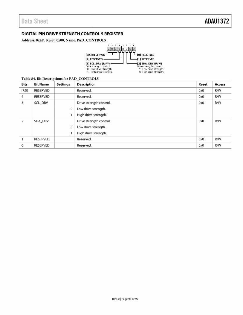
Data Sheet ADAU1372
DIGITAL PIN DRIVE STRENGTH CONTROL 5 REGISTER Address: 0x4D, Reset: 0x00, Name: PAD_CONTROL5
Table 84. Bit Descriptions for PAD_CONTROL5 Bits Bit Name Settings Description Reset Access
[7:5] RESERVED Reserved. 0x0 R/W
4 RESERVED Reserved. 0x0 R/W
3 SCL_DRV Drive strength control. 0x0 R/W
0 Low drive strength.
1 High drive strength.
2 SDA_DRV Drive strength control. 0x0 R/W
0 Low drive strength.
1 High drive strength.
1 RESERVED Reserved. 0x0 R/W
0 RESERVED Reserved. 0x0 R/W
Rev. 0 | Page 91 of 92
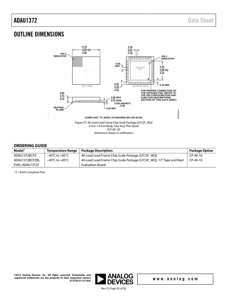
ADAU1372 Data Sheet
OUTLINE DIMENSIONS
Figure 77. 40-Lead Lead Frame Chip Scale Package [LFCSP_WQ]
6 mm × 6 mm Body, Very Very Thin Quad (CP-40-10)
Dimension shown in millimeters
ORDERING GUIDE Model1 Temperature Range Package Description Package Option ADAU1372BCPZ −40°C to +85°C 40-Lead Lead Frame Chip Scale Package [LFCSP_WQ] CP-40-10 ADAU1372BCPZRL −40°C to +85°C 40-Lead Lead Frame Chip Scale Package [LFCSP_WQ], 13" Tape and Reel CP-40-10 EVAL-ADAU1372Z Evaluation Board
1 Z = RoHS Compliant Part.
05-0
6-20
11-A
0.50BSC
BOTTOM VIEWTOP VIEW
PIN 1INDICATOR
EXPOSEDPAD
PIN 1INDICATOR
SEATINGPLANE
0.05 MAX0.02 NOM
0.20 REF
COPLANARITY0.08
0.300.230.18
6.106.00 SQ5.90
0.800.750.70
FOR PROPER CONNECTION OFTHE EXPOSED PAD, REFER TOTHE PIN CONFIGURATION ANDFUNCTION DESCRIPTIONSSECTION OF THIS DATA SHEET.
0.450.400.35
0.25 MIN
4.454.30 SQ4.25
COMPLIANT TO JEDEC STANDARDS MO-220-WJJD.
401
1120
21
3031
10
PKG
-003
438
©2014 Analog Devices, Inc. All rights reserved. Trademarks and registered trademarks are the property of their respective owners. D12702-0-12/14(0)
Rev. 0 | Page 92 of 92


![[Federal Register Volume 76, Number 55 (Tuesday, …services.casa.gov.au/airworth/airwd/ADfiles/over/b737/...1 [Federal Register Volume 76, Number 55 (Tuesday, March 22, 2011)] [Rules](https://img.pdfslide.net/doc/110x75/5e338cdeffd31e3e4d06957e/federal-register-volume-76-number-55-tuesday-1-federal-register-volume.jpg)