Embed Size (px)
Citation preview
ADC Board VHDL Firmwaredevelopment for Mona Lisa
Roy Wastie
Overview
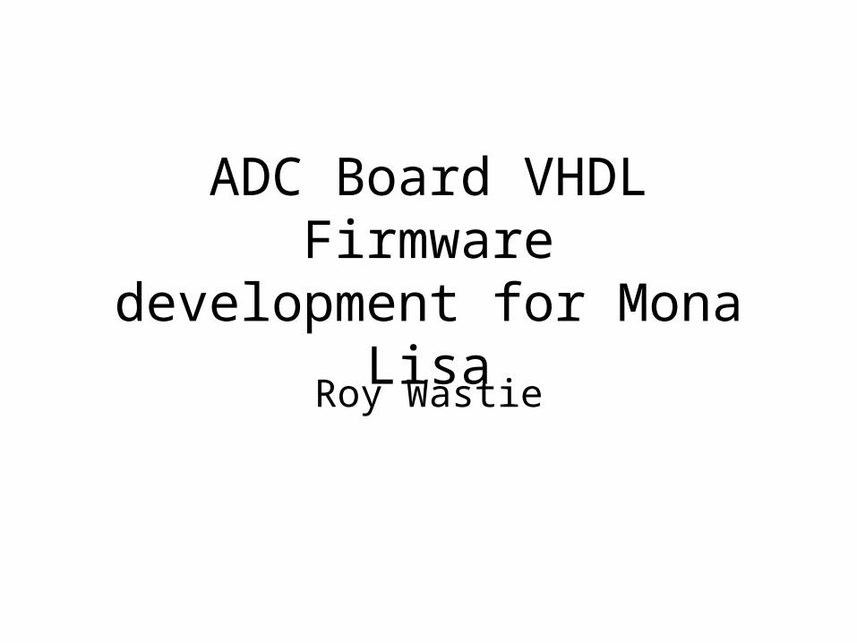
• Introduction• ADC Board• Hardware Blocks• Basic FPGA Architectures• Xilinx ISE 10.1 Tool Flow• USB• Algorithm• VHDL
Introduction
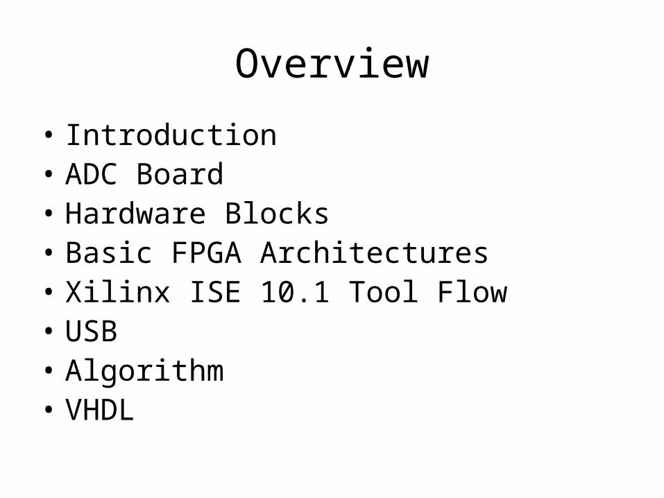
• Applications of FPGAs include digital signal processing, software-defined radio, aerospace and defense systems, ASIC prototyping, medical imaging, computer vision, speech recognition, cryptography, bioinformatics, computer hardware emulation & glue logic for PCBs.
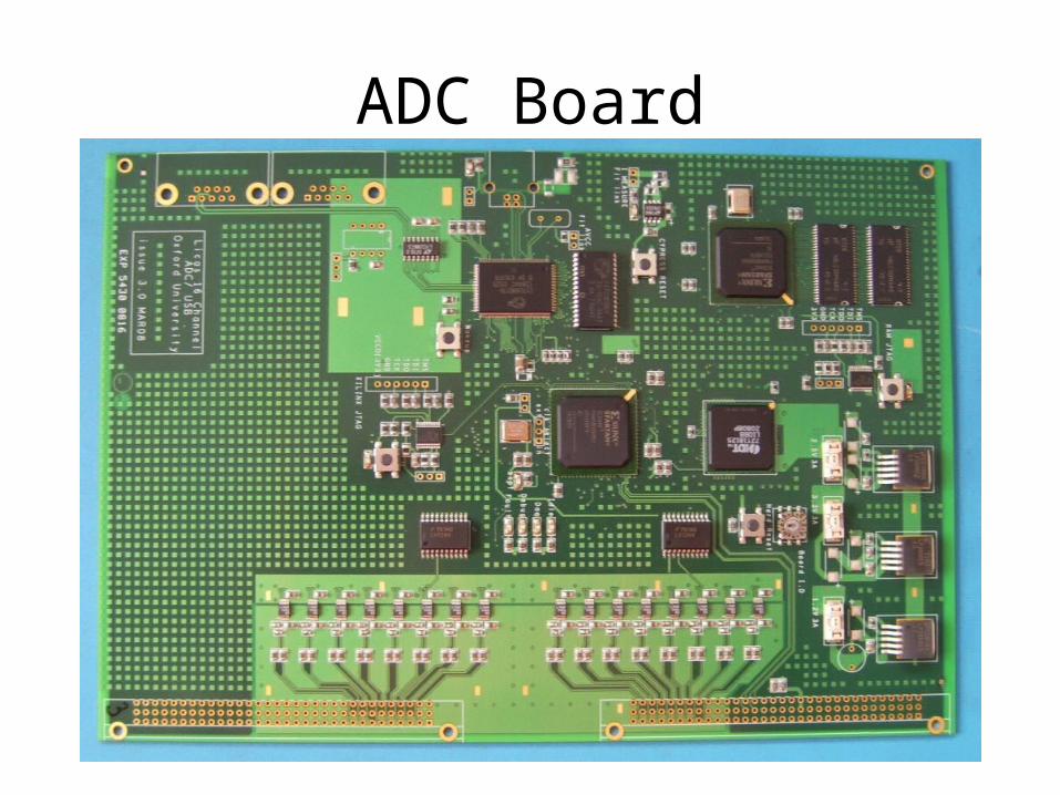
ADC Board
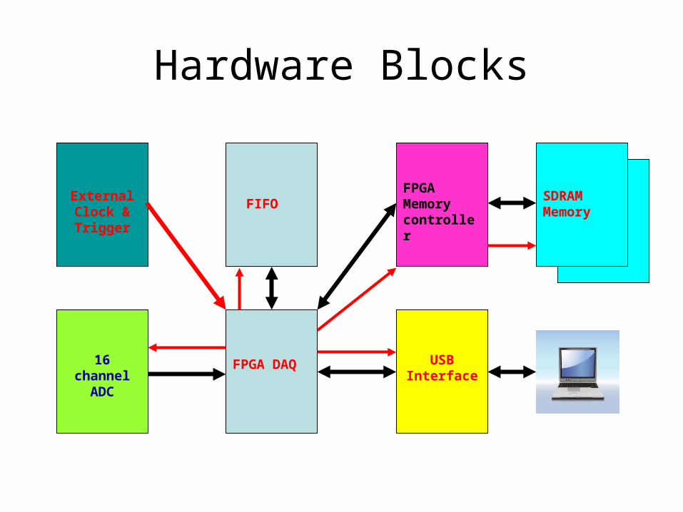
Hardware Blocks
FPGA DAQ16 channel
ADC
FIFOFPGA Memory controller
USB Interface
SDRAM Memory
External Clock & Trigger
Basic FPGA Architectures
Overview
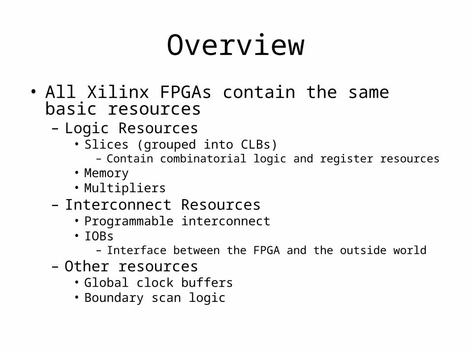
• All Xilinx FPGAs contain the same basic resources– Logic Resources
• Slices (grouped into CLBs)– Contain combinatorial logic and register resources
• Memory• Multipliers
– Interconnect Resources• Programmable interconnect • IOBs
– Interface between the FPGA and the outside world
– Other resources• Global clock buffers• Boundary scan logic
Basic Building Block
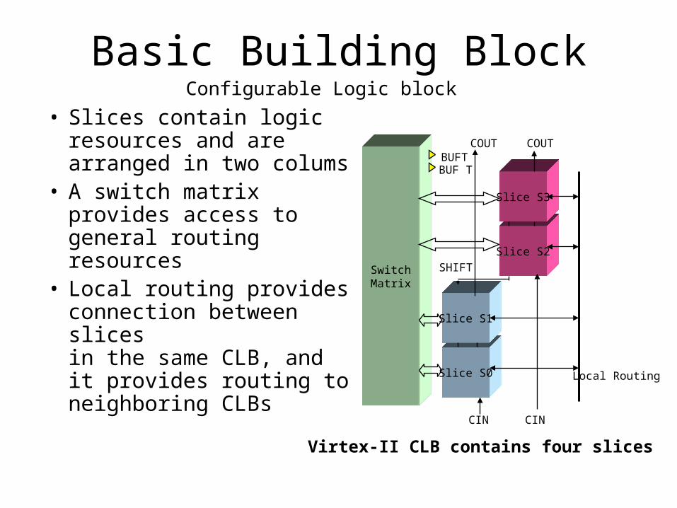
• Slices contain logic resources and are arranged in two colums
• A switch matrix provides access to general routing resources
• Local routing provides connection between slices in the same CLB, and it provides routing to neighboring CLBs CIN
SwitchMatrix
BUFTBUF T
COUTCOUT
Slice S0
Slice S1
Local Routing
Slice S2
Slice S3
CIN
SHIFT
Configurable Logic block
Virtex-II CLB contains four slices
Slice 0
LUTLUT CarryCarry
LUTLUT CarryCarry D QCE
PRE
CLR
DQCE
PRE
CLR
Basic Building Blocks
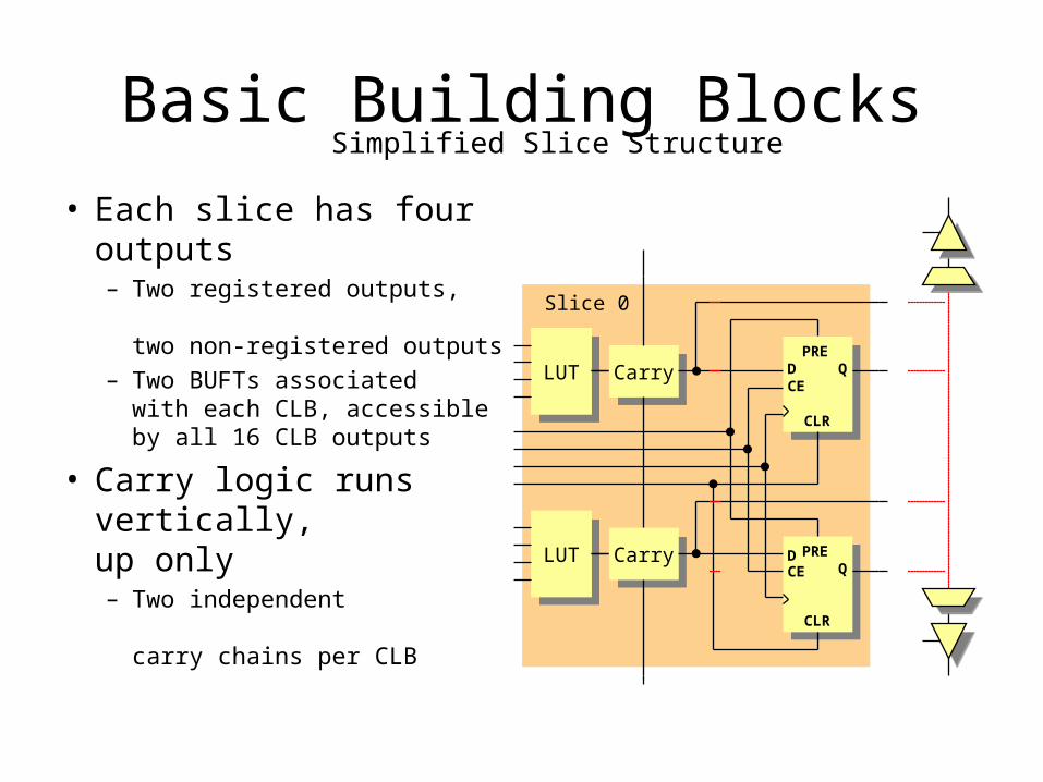
• Each slice has four outputs– Two registered outputs,
two non-registered outputs
– Two BUFTs associated with each CLB, accessible by all 16 CLB outputs
• Carry logic runs vertically, up only– Two independent
carry chains per CLB
Simplified Slice Structure
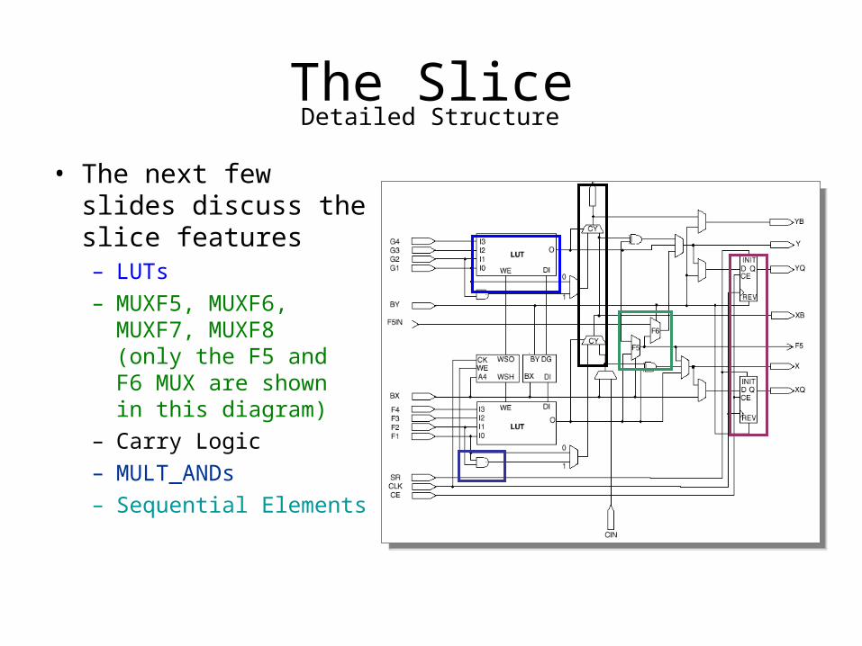
The Slice
• The next few slides discuss the slice features– LUTs– MUXF5, MUXF6,
MUXF7, MUXF8 (only the F5 and F6 MUX are shown in this diagram)
– Carry Logic– MULT_ANDs– Sequential Elements
Detailed Structure
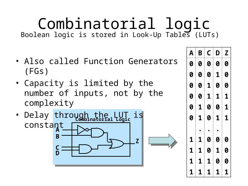
Combinatorial Logic
AB
CD
Z
Combinatorial logic
• Also called Function Generators (FGs)• Capacity is limited by the number of
inputs, not by the complexity• Delay through the LUT is constant
A B C D Z
0 0 0 0 0
0 0 0 1 0
0 0 1 0 0
0 0 1 1 1
0 1 0 0 1
0 1 0 1 1
. . .
1 1 0 0 0
1 1 0 1 0
1 1 1 0 0
1 1 1 1 1
Boolean logic is stored in Look-Up Tables (LUTs)
D
CE
PRE
CLR
Q
FDCPE
D
CE
S
R
Q
FDRSE
D
CE
PRE
CLR
Q
LDCPE
G
_1
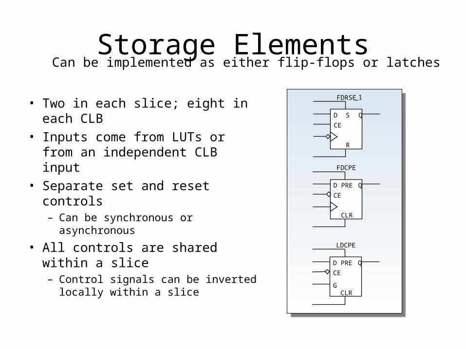
Storage Elements
• Two in each slice; eight in each CLB
• Inputs come from LUTs or from an independent CLB input
• Separate set and reset controls– Can be synchronous or
asynchronous
• All controls are shared within a slice– Control signals can be inverted
locally within a slice
Can be implemented as either flip-flops or latches
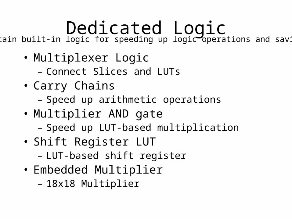
Dedicated Logic
• Multiplexer Logic– Connect Slices and LUTs
• Carry Chains– Speed up arithmetic operations
• Multiplier AND gate– Speed up LUT-based multiplication
• Shift Register LUT– LUT-based shift register
• Embedded Multiplier– 18x18 Multiplier
FPGAs contain built-in logic for speeding up logic operations and saving resources
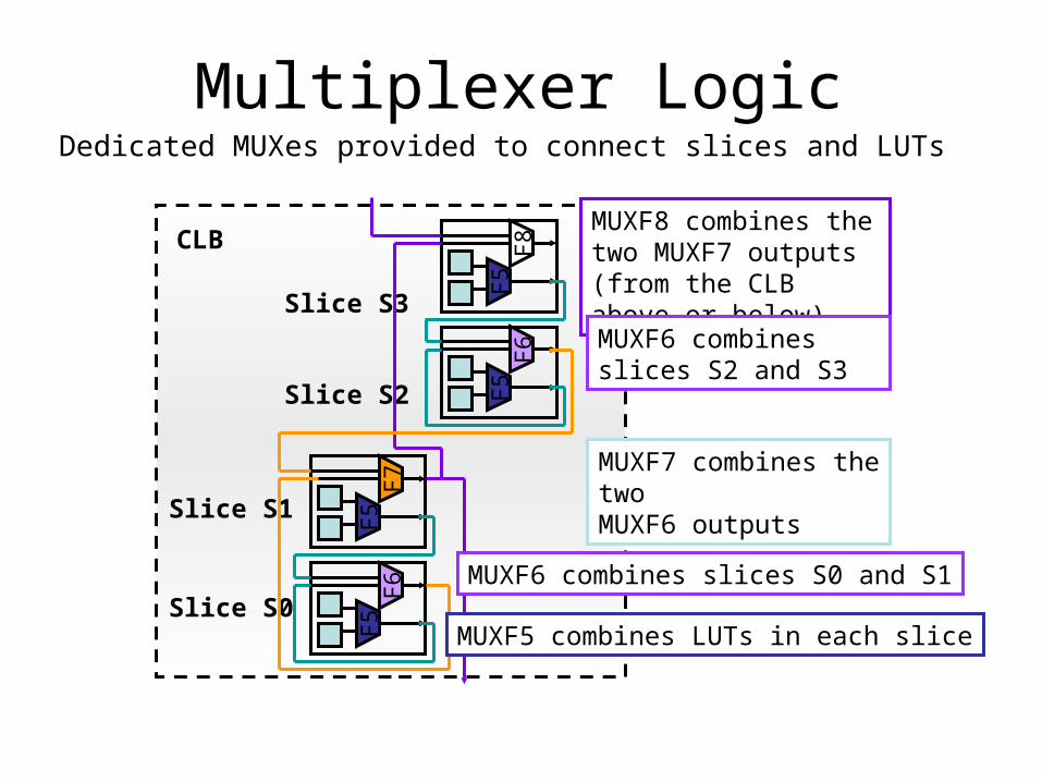
Multiplexer Logic
F5F8
F5F6
CLB
Slice S3
Slice S2
Slice S0
Slice S1 F5F7
F5F6
MUXF8 combines the two MUXF7 outputs (from the CLB above or below)
MUXF6 combines slices S2 and S3
MUXF7 combines the two MUXF6 outputs
MUXF6 combines slices S0 and S1
MUXF5 combines LUTs in each slice
Dedicated MUXes provided to connect slices and LUTs
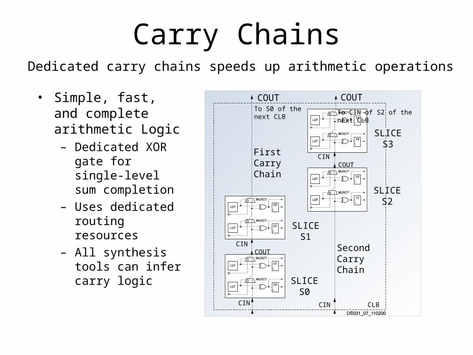
Carry Chains
• Simple, fast, and complete arithmetic Logic– Dedicated XOR gate
for single-level sum completion
– Uses dedicated routing resources
– All synthesis tools can infer carry logic
COUT COUT
SLICE S0
SLICE S1
Second Carry Chain
To S0 of the next CLB
To CIN of S2 of the next CLB
First Carry Chain
SLICE S3
SLICE S2
COUT
COUTCIN
CIN
CIN CIN CLB
Dedicated carry chains speeds up arithmetic operations
CODI CIS
LUT
CY_MUX
CY_XOR
MULT_AND
A
B
A x B
LUT
LUT
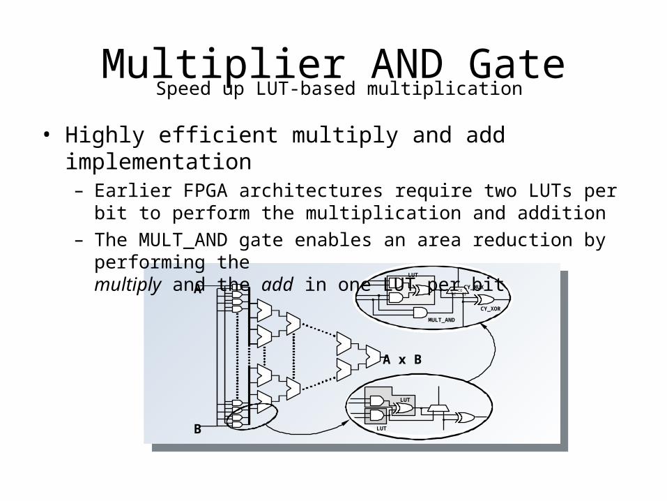
Multiplier AND Gate
• Highly efficient multiply and add implementation– Earlier FPGA architectures require two LUTs per bit to perform
the multiplication and addition– The MULT_AND gate enables an area reduction by performing
the multiply and the add in one LUT per bit
Speed up LUT-based multiplication
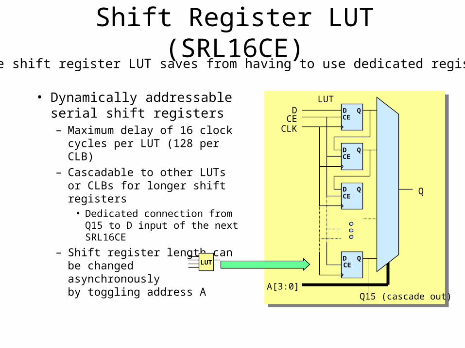
Shift Register LUT (SRL16CE)
• Dynamically addressable serial shift registers– Maximum delay of 16 clock
cycles per LUT (128 per CLB)– Cascadable to other LUTs or
CLBs for longer shift registers• Dedicated connection from
Q15 to D input of the next SRL16CE
– Shift register length can be changed asynchronously by toggling address A
LUT
D QCE
D QCE
D QCE
D QCE
LUTD
CECLK
A[3:0]
Q
Q15 (cascade out)
The shift register LUT saves from having to use dedicated registers
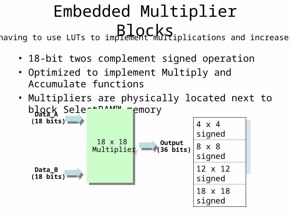
Embedded Multiplier Blocks
• 18-bit twos complement signed operation• Optimized to implement Multiply and Accumulate
functions• Multipliers are physically located next to block
SelectRAM™ memory
18 x 18 Multiplier
18 x 18 Multiplier
Output (36 bits)
Data_A (18 bits)
Data_B (18 bits)
4 x 4 signed
8 x 8 signed
12 x 12 signed
18 x 18 signed
Saves from having to use LUTs to implement multiplications and increases performance
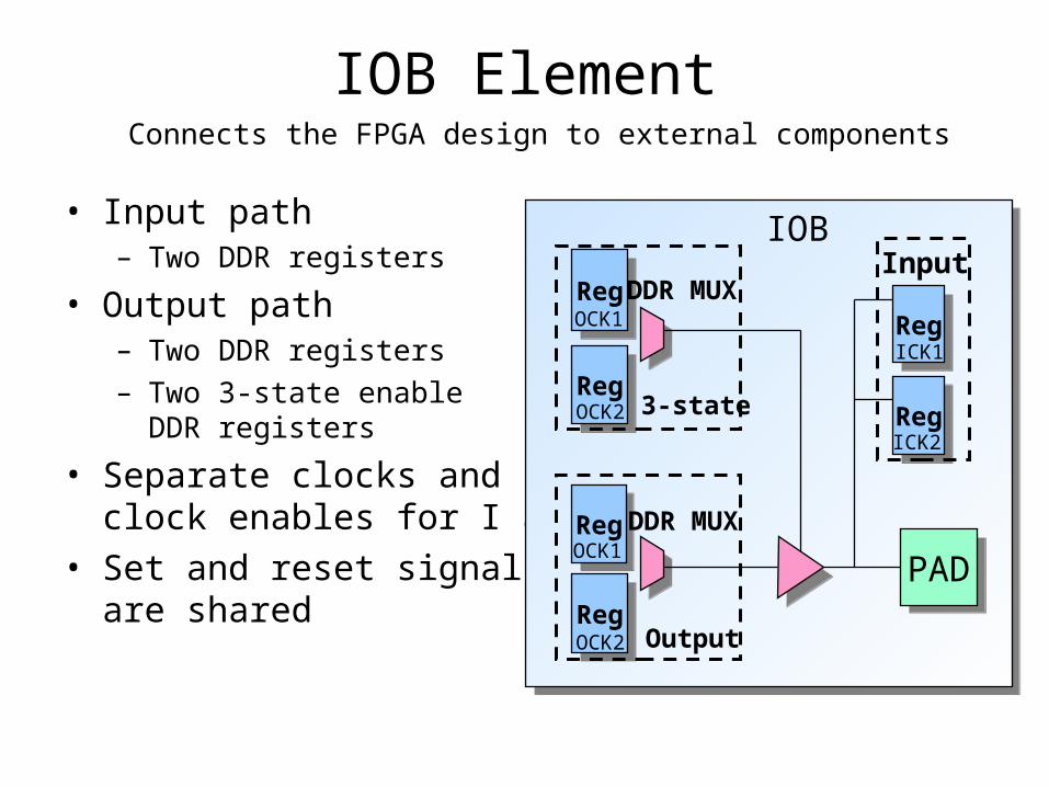
IOB Element
• Input path– Two DDR registers
• Output path– Two DDR registers– Two 3-state enable
DDR registers
• Separate clocks and clock enables for I and O
• Set and reset signals are shared
RegReg
RegReg
DDR MUX
3-state
OCK1
OCK2
RegReg
RegReg
DDR MUX
Output
OCK1
OCK2
PADPAD
RegReg
RegReg
Input
ICK1
ICK2
IOB
Connects the FPGA design to external components
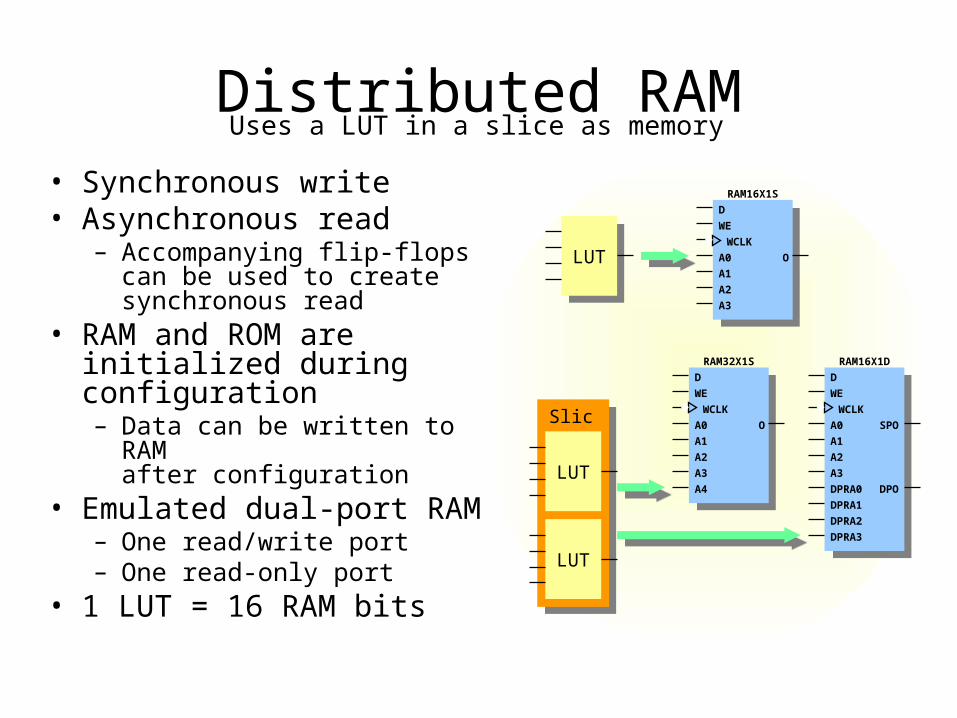
Distributed RAM• Synchronous write• Asynchronous read
– Accompanying flip-flops can be used to create synchronous read
• RAM and ROM are initialized duringconfiguration– Data can be written to RAM
after configuration• Emulated dual-port RAM
– One read/write port– One read-only port
• 1 LUT = 16 RAM bits
RAM16X1S
O
D
WE
WCLK
A0
A1
A2
A3
LUTLUT
RAM32X1S
O
D
WE
WCLK
A0
A1
A2
A3
A4
RAM16X1D
SPO
D
WE
WCLK
A0
A1
A2
A3
DPRA0 DPO
DPRA1
DPRA2
DPRA3
Slice
LUT
LUT
Uses a LUT in a slice as memory
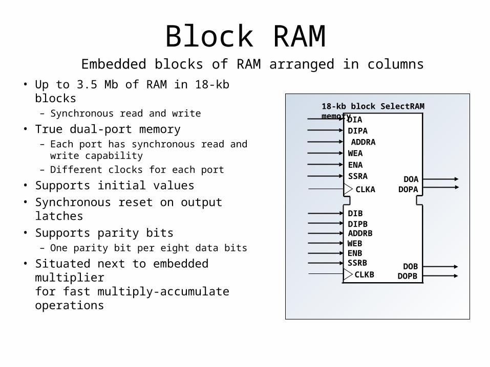
Block RAM
• Up to 3.5 Mb of RAM in 18-kb blocks– Synchronous read and write
• True dual-port memory– Each port has synchronous read and
write capability
– Different clocks for each port
• Supports initial values• Synchronous reset on output latches• Supports parity bits
– One parity bit per eight data bits
• Situated next to embedded multiplierfor fast multiply-accumulate operations
DIADIPAADDRAWEA
ENASSRA
CLKA
DIBDIPB
WEBADDRB
ENBSSRB
DOA
CLKB
DOPA
DOPBDOB
18-kb block SelectRAM memory
Embedded blocks of RAM arranged in columns
Global Routing
• Sixteen dedicated global clock multiplexers– Eight on the top-center of the die, eight on the bottom-center– Driven by a clock input pad, a DCM, or local routing
• Global clock multiplexers provide the following:– Traditional clock buffer (BUFG) function– Global clock enable capability (BUFGCE)– Glitch-free switching between clock signals (BUFGMUX)
• Up to eight clock nets can be used in each clock region of the device– Each device contains four or more clock regions
Digital Clock Manager (DCM)
• Up to twelve DCMs per device– Located on the top and bottom edges of the die– Driven by clock input pads
• DCMs provide the following:– Delay-Locked Loop (DLL)– Digital Frequency Synthesizer (DFS)– Digital Phase Shifter (DPS)
• Up to four outputs of each DCM can drive onto global clock buffers– All DCM outputs can drive general routing
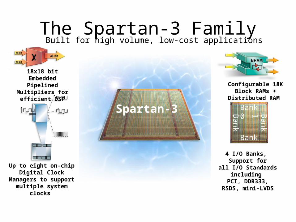
The Spartan-3 Family
18x18 bit Embedded Pipelined Multipliers
for efficient DSP Configurable 18K Block RAMs + Distributed RAM
4 I/O Banks, Support for
all I/O Standards including
PCI, DDR333,RSDS, mini-LVDS
Bank 0 Bank 1
Bank 2
Bank 3
Up to eight on-chip Digital Clock Managers
to support multiple system clocks
Spartan-3
Built for high volume, low-cost applications
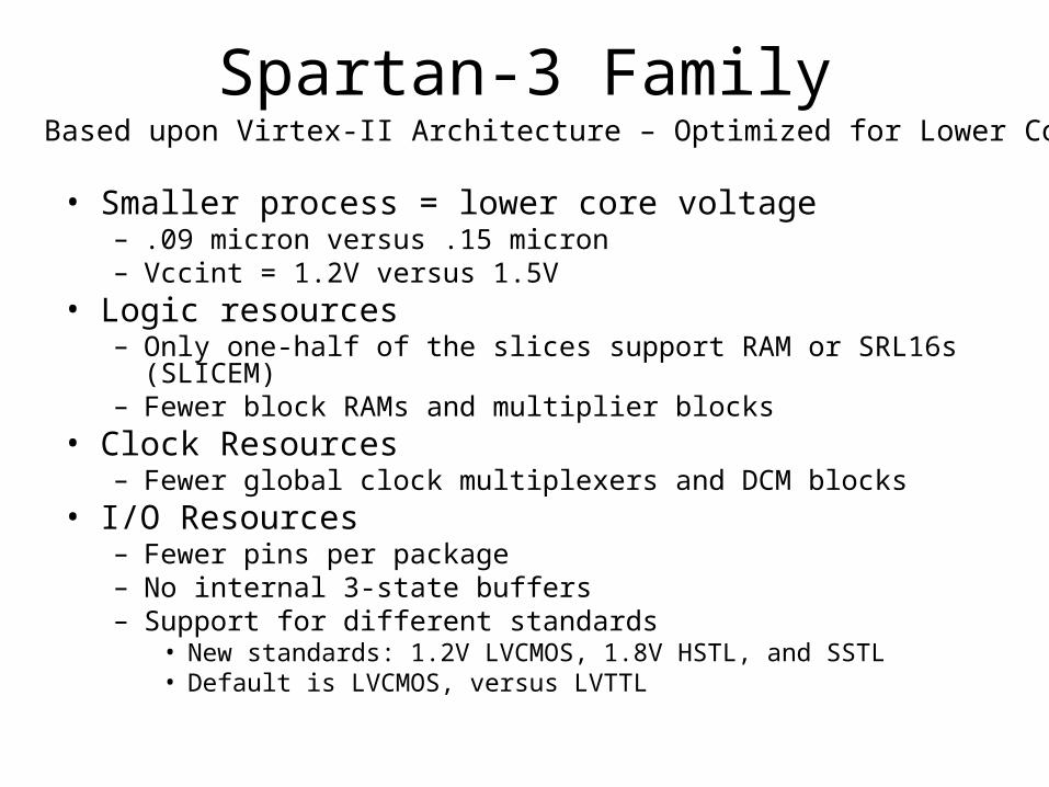
Spartan-3 Family
• Smaller process = lower core voltage– .09 micron versus .15 micron– Vccint = 1.2V versus 1.5V
• Logic resources– Only one-half of the slices support RAM or SRL16s (SLICEM)– Fewer block RAMs and multiplier blocks
• Clock Resources– Fewer global clock multiplexers and DCM blocks
• I/O Resources– Fewer pins per package– No internal 3-state buffers – Support for different standards
• New standards: 1.2V LVCMOS, 1.8V HSTL, and SSTL• Default is LVCMOS, versus LVTTL
Based upon Virtex-II Architecture – Optimized for Lower Cost
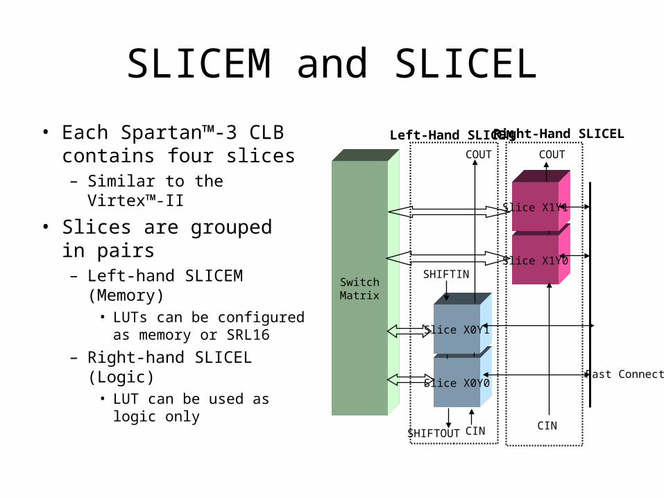
SLICEM and SLICEL
• Each Spartan™-3 CLB contains four slices– Similar to the Virtex™-II
• Slices are grouped in pairs– Left-hand SLICEM
(Memory)• LUTs can be configured
as memory or SRL16
– Right-hand SLICEL (Logic)
• LUT can be used as logic only CIN
SwitchMatrix
COUTCOUT
Slice X0Y0
Slice X0Y1
Fast Connects
Slice X1Y0
Slice X1Y1
CIN
SHIFTIN
Left-Hand SLICEM Right-Hand SLICEL
SHIFTOUT
Xilinx Tool Flow
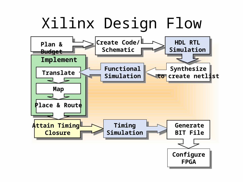
Translate
Map
Place & Route
Xilinx Design FlowPlan & Budget HDL RTL
Simulation
Synthesizeto create netlist
FunctionalSimulation
Attain Timing Closure
TimingSimulation
Implement
Create Code/Schematic
GenerateBIT File
ConfigureFPGA
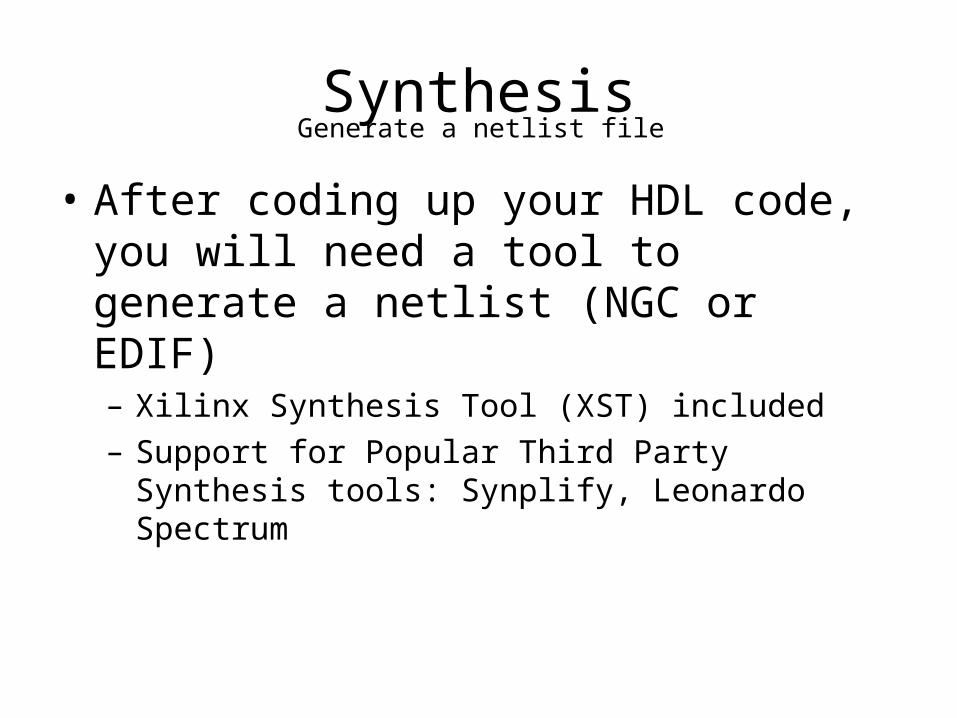
Synthesis
• After coding up your HDL code, you will need a tool to generate a netlist (NGC or EDIF) – Xilinx Synthesis Tool (XST) included– Support for Popular Third Party Synthesis tools:
Synplify, Leonardo Spectrum
Generate a netlist file
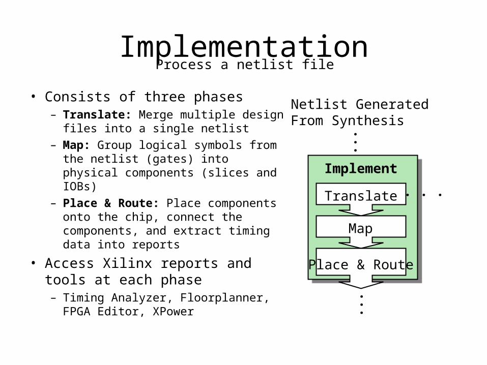
Implementation
• Consists of three phases– Translate: Merge multiple design
files into a single netlist– Map: Group logical symbols from the
netlist (gates) into physical components (slices and IOBs)
– Place & Route: Place components onto the chip, connect the components, and extract timing data into reports
• Access Xilinx reports and tools at each phase– Timing Analyzer, Floorplanner,
FPGA Editor, XPower
Translate
Map
Place & Route
Implement
. . .
.
.
.
Netlist GeneratedFrom Synthesis
.
.
.
Process a netlist file
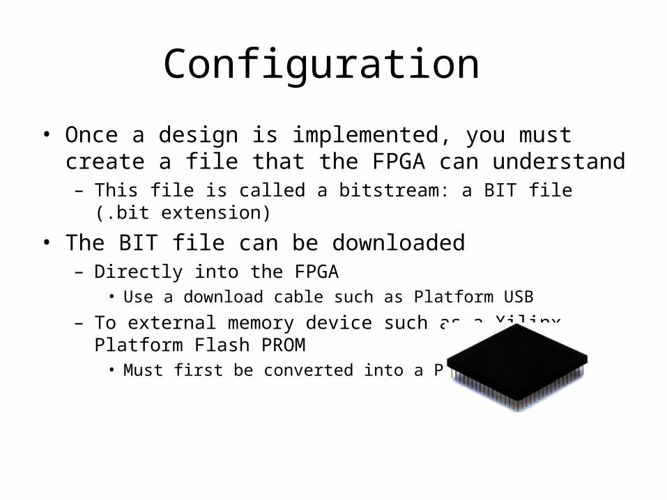
Configuration
• Once a design is implemented, you must create a file that the FPGA can understand– This file is called a bitstream: a BIT file (.bit extension)
• The BIT file can be downloaded – Directly into the FPGA
• Use a download cable such as Platform USB
– To external memory device such as a Xilinx Platform Flash PROM
• Must first be converted into a PROM file
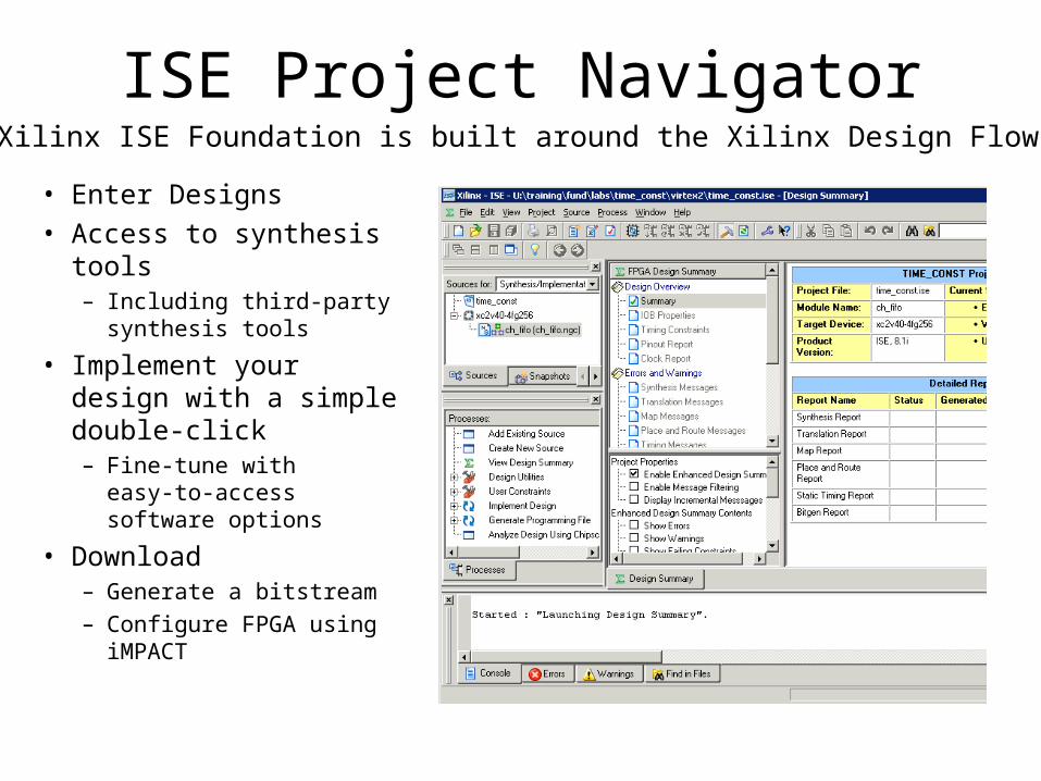
ISE Project Navigator
• Enter Designs• Access to synthesis tools
– Including third-party synthesis tools
• Implement your design with a simple double-click– Fine-tune with
easy-to-access software options
• Download– Generate a bitstream– Configure FPGA using
iMPACT
Xilinx ISE Foundation is built around the Xilinx Design Flow
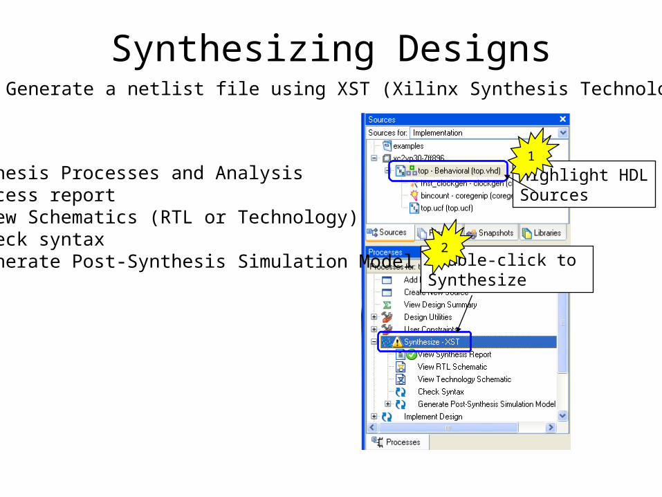
Synthesizing Designs
Double-click to Synthesize
Synthesis Processes and Analysis • Access report• View Schematics (RTL or Technology)• Check syntax• Generate Post-Synthesis Simulation Model
Generate a netlist file using XST (Xilinx Synthesis Technology)
Highlight HDLSources
1
2
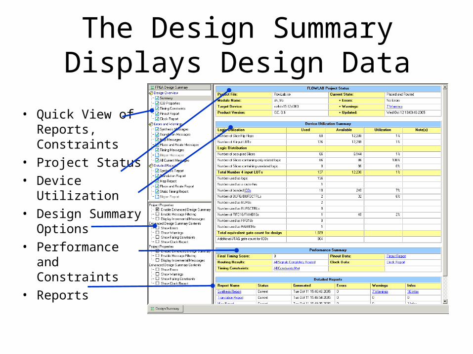
The Design Summary Displays Design Data
• Quick View of Reports, Constraints
• Project Status
• Device Utilization
• Design Summary Options
• Performance and Constraints
• Reports
Outline
• Overview• ISE• Summary• Lab 1: Xilinx Tool Flow

USB
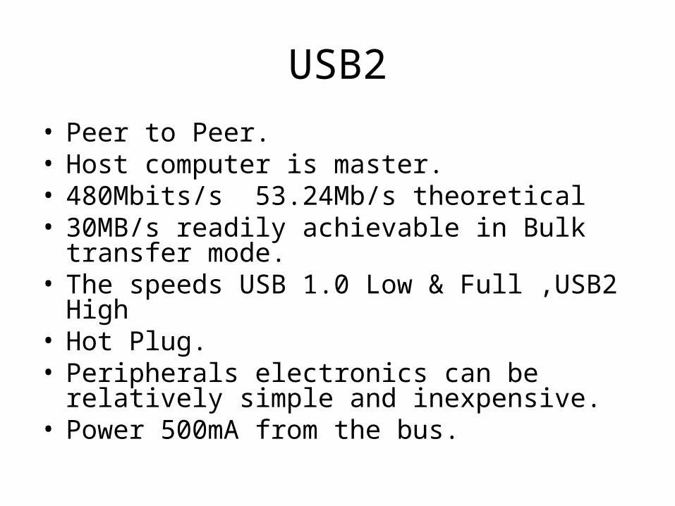
USB2
• Peer to Peer.• Host computer is master.• 480Mbits/s 53.24Mb/s theoretical• 30MB/s readily achievable in Bulk transfer
mode.• The speeds USB 1.0 Low & Full ,USB2 High• Hot Plug.• Peripherals electronics can be relatively simple
and inexpensive.• Power 500mA from the bus.
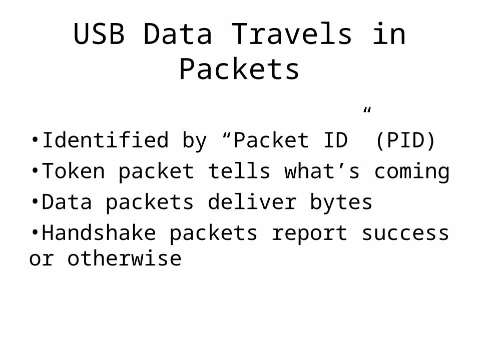
USB Data Travels in Packets
•Identified by “Packet ID” (PID)
•Token packet tells what’s coming
•Data packets deliver bytes
•Handshake packets report success or otherwise
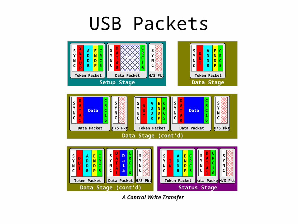
USB PacketsSETUP
ADDR
CRC5
SYNC
ENDP
DATA0
CRC16
SYNC
DataACK
SYNC
Token Packet Data Packet H/S Pkt
Setup Stage Data Stage
Data Stage (cont'd)
Data Stage (cont'd)
A Control Write Transfer
DATA1
CRC16
SYNC
Data
Data Packet
ACK
SYNC
H/S Pkt
OUT
ADDR
CRC5
SYNC
ENDP
Token Packet
DATA0
CRC16
SYNC
Data
Data Packet
ACK
SYNC
H/S Pkt
OUT
ADDR
CRC5
SYNC
ENDP
Token Packet
DATA1
CRC16
SYNC
Data
ACK
SYNC
H/S PktData Packet
OUT
ADDR
CRC5
SYNC
ENDP
Token Packet
IN
ADDR
CRC5
SYNC
ENDP
DATA1
CRC16
SYNC
ACK
SYNC
Data Packet H/S PktToken Packet
Status Stage
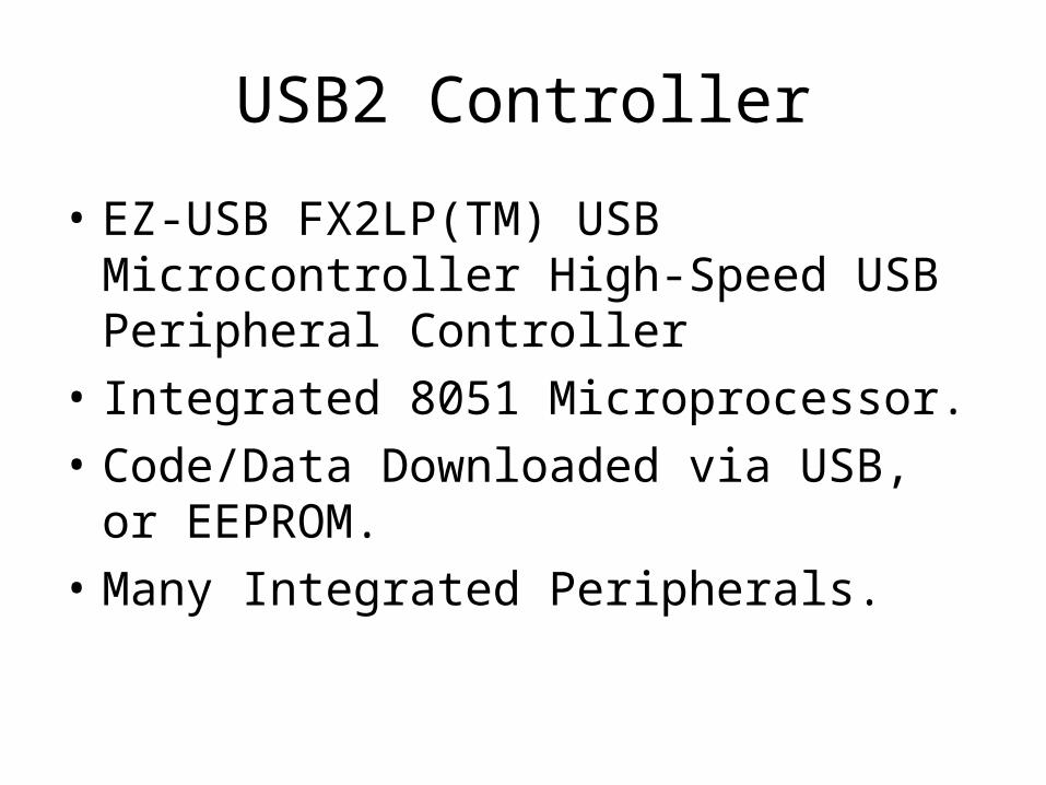
USB2 Controller
• EZ-USB FX2LP(TM) USB Microcontroller High-Speed USB Peripheral Controller
• Integrated 8051 Microprocessor.
• Code/Data Downloaded via USB, or EEPROM.
• Many Integrated Peripherals.
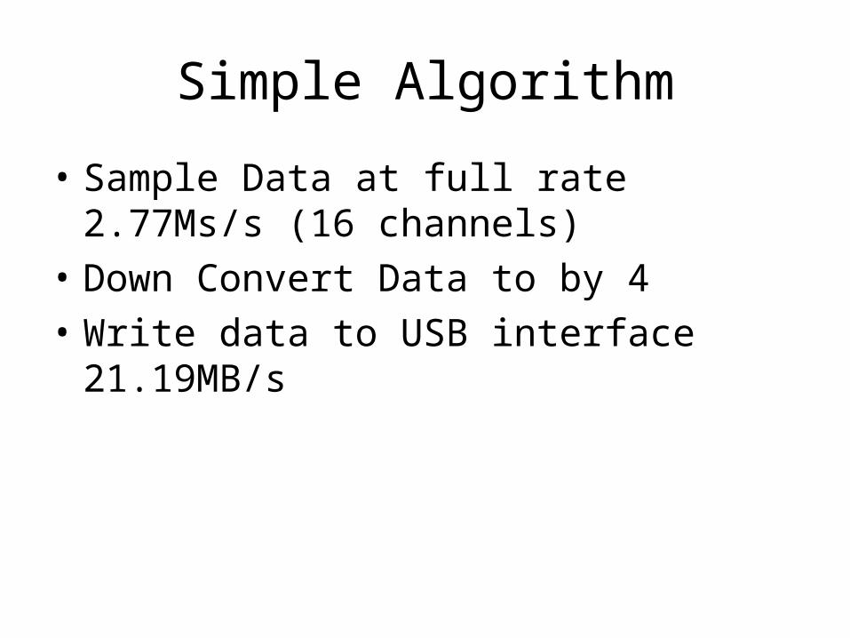
Simple Algorithm
• Sample Data at full rate 2.77Ms/s (16 channels)
• Down Convert Data to by 4
• Write data to USB interface 21.19MB/s
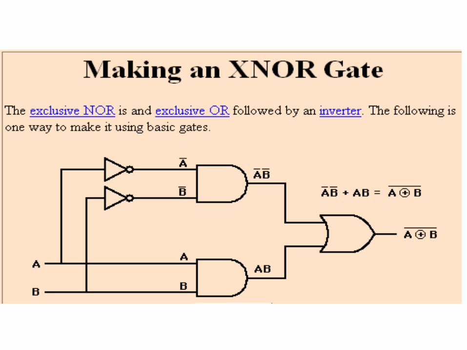
VHDL
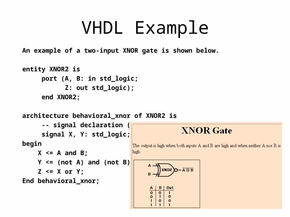
VHDL ExampleAn example of a two-input XNOR gate is shown below.
entity XNOR2 is
port (A, B: in std_logic;
Z: out std_logic);
end XNOR2;
architecture behavioral_xnor of XNOR2 is
-- signal declaration (of internal signals X, Y)
signal X, Y: std_logic;
begin
X <= A and B;
Y <= (not A) and (not B);
Z <= X or Y;
End behavioral_xnor;