Embed Size (px)
Citation preview

ADC083000
www.ti.com SNAS358N –JUNE 2006–REVISED JULY 2009
ADC083000 8-Bit, 3 GSPS, High Performance, Low Power A/D ConverterCheck for Samples: ADC083000
1FEATURES DESCRIPTIONThe ADC083000 is a single, low power, high
2• Single +1.9V ±0.1V Operationperformance CMOS analog-to-digital converter that
• Choice of SDR or DDR Output Clocking digitizes signals to 8 bits resolution at sampling rates• Serial Interface for Extended Control up to 3.4 GSPS. Consuming a typical 1.9 Watts at 3
GSPS from a single 1.9 Volt supply, this device is• Adjustment of Input Full-Scale Range andspecified to have no missing codes over the fullOffsetoperating temperature range. The unique folding and
• Duty Cycle Corrected Sample Clock interpolating architecture, the fully differential• Test Pattern comparator design, the innovative design of the
internal sample-and-hold amplifier and the self-calibration scheme enable an excellent response ofAPPLICATIONSall dynamic parameters up to Nyquist, producing a
• Direct RF Down Conversion high 7.0 Effective Number Of Bits, (ENOB) with a 748• Digital Oscilloscopes MHz input signal and a 3 GHz sample rate while
providing a 10-18 Word Error Rate. The ADC083000• Satellite Set-Top Boxesachieves a 3 GSPS sampling rate by utilizing both the• Communications Systemsrising and falling edge of a 1.5 GHz input clock.
• Test Instrumentation Output formatting is offset binary and the LVDSdigital outputs are compatible with IEEE 1596.3-1996,
KEY SPECIFICATIONS with the exception of an adjustable common modevoltage between 0.8V and 1.15V.• Resolution 8 BitsThe ADC has a 1:4 demultiplexer that feeds four• Max Conversion Rate 3 GSPS (min)LVDS buses and reduces the output data rate on• Error Rate 10-18 (typ) each bus to a quarter of the sampling rate.
• ENOB @ 748 MHz Input 7.0 Bits (typ)The converter typically consumes less than 25 mW in
• SNR @ 748 MHz 44.5 dB (typ) the Power Down Mode and is available in a 128-lead,• Full Power Bandwidth 3 GHz (typ) thermally enhanced exposed pad HLQFP and
operates over the Industrial (-40°C ≤ TA ≤ +85°C)• Power Consumptiontemperature range.– Operating 1.9 W (typ)
– Power Down Mode 25 mW (typ)
1
Please be aware that an important notice concerning availability, standard warranty, and use in critical applications ofTexas Instruments semiconductor products and disclaimers thereto appears at the end of this data sheet.
2All trademarks are the property of their respective owners.
PRODUCTION DATA information is current as of publication date. Copyright © 2006–2009, Texas Instruments IncorporatedProducts conform to specifications per the terms of the TexasInstruments standard warranty. Production processing does notnecessarily include testing of all parameters.

2
VREF
CLK/2
8-BIT
ADC1
VIN+
VIN-
DCLK+OutputClock
Generator DCLK-
Data Bus Output16 LVDS Pairs
DEMUX
ORControlLogic
8-BIT
ADC2
Data Bus Output16 LVDS Pairs
3
CalRun
+
-
+
-
S/H
S/H
VBG
CLK+
CLK-
ControlInputs
SerialInterface
DEMUX
Dd
Db
Dc
Da
LATCH
DEMUX LATCH
8
8
ADC083000
SNAS358N –JUNE 2006–REVISED JULY 2009 www.ti.com
Block Diagram
2 Submit Documentation Feedback Copyright © 2006–2009, Texas Instruments Incorporated
Product Folder Links: ADC083000

GNDVA
OUTV/SCLKOutEdge/DDR/SDATA
VA
GNDVCMO
GND
VIN-VIN+
GND
DR
GN
D
12
16
DR
GN
D
FSR/ECE
CLK+CLK-
GNDDCLK_RST+DCLK_RST-
GND
PDGND
ADC083000
20
24
28
CALVBG
REXT
DR
GN
D
32313029
272625
232221
191817
151413
1110
1
4
89
765
32
Tdi
ode_
pT
diod
e_n
Da0
+D
a0-
Da1
+D
a1-
NC
DR
GN
DD
a2+
Da2
-D
a3+
Da3
-D
a4+
Da4
-D
a5+
Da5
-
NC
37 41
DR
GN
DD
a6+
Da6
-D
a7+
Da7
-D
c0+
Dc0
-D
c1+
Dc1
-
NC
33 34 35 36 38 39 40 42 43 44 46 47 48 50 51 52 54 55 56 58 59 60 62 63 6445 49 53 57 61
Dc7+Dc7-OR+OR-DCLK-DCLK+Dd7-Dd7+Dd6-Dd6+DR GND
Dd5-Dd5+Dd4-Dd4+Dd3-Dd3+Dd2-Dd2+
71
81
86
91
96
Dc4+Dc4-Dc5+Dc5-
DR GNDDc6+Dc6-
Dc2+Dc2-Dc3+Dc3-
76
6665
67686970
7372
7475
7877
7980
8382
8485
8887
8990
9392
9495
128
123
118
108
113
124
127
126
125
119
122
121
120
114
117
116
115
109
112
111
110
104
107
106
105 99
102
101
100
103 98 97
VA
VA
VA
NC
VA
VA
VA
VADCLK_RST
VA
VD
R
VD
R
VD
R
VDR
VDR
Cal
Dly
/SC
SC
alR
unD
b0+
Db0
-D
b1+
Db1
-V
DR
NC
Db2
+D
b2-
Db3
+D
b3-
Db4
+D
b4-
Db5
+D
b5-
NC
Db6
+D
b6-
Db7
+D
b7-
Dd0
+D
d0-
Dd1
+D
d1-
VD
R
NC
VD
R
VA
DR
GN
D
ADC083000
Exposed pad bottom side.(See Note below.)
ADC083000
www.ti.com SNAS358N –JUNE 2006–REVISED JULY 2009
Pin Configuration
NOTEThe exposed pad on the bottom of the package must be soldered to a ground planeto ensure rated performance.
Copyright © 2006–2009, Texas Instruments Incorporated Submit Documentation Feedback 3
Product Folder Links: ADC083000

GND
VA
50k
50k
GND
VA
50k
50k
200k
8 pF
GND
VA
GND
VA
50k
50k
200k
8 pF
VA
SDATA
DDR
GND
VA
50k
ADC083000
SNAS358N –JUNE 2006–REVISED JULY 2009 www.ti.com
Pin Descriptions and Equivalent CircuitsPin Functions
Pin No. Symbol Equivalent Circuit Description
Output Voltage Amplitude / Serial Interface Clock(Input):LVCMOS Tie this pin high for normal differential DCLK anddata amplitude. Ground this pin for a reduced differential outputamplitude and reduced power consumption. See The LVDS
3 OutV / SCLK Outputs. When the extended control mode is enabled, this pinfunctions as the SCLK input which clocks in the serial data. SeeNORMAL/EXTENDED CONTROL for details on the extendedcontrol mode. See THE SERIAL INTERFACE for description of theserial interface.
Edge Select / Double Data Rate / Serial Data(Input):LVCMOS This input sets the output edge of DCLK+ atwhich the output data transitions. (See OutEdge Setting). When
OutEdge / DDR / this pin is floating or connected to 1/2 the supply voltage, DDR4 SDATA clocking is enabled. When the extended control mode is enabled,this pin functions as the SDATA input. See NORMAL/EXTENDEDCONTROL for details on the extended control mode. See THESERIAL INTERFACE for description of the serial interface.
DCLK Reset(Input):LVCMOS A positive pulse on this pin is used to reset andsynchronize the DCLK outs of multiple converters. See MULTIPLE15 DCLK_RST ADC SYNCHRONIZATION for detailed description. When bit 14 inthe Configuration Register (address 1h) is set to 0b, this single-ended DCLK_RST pin is selected. See also pins 22,23 description.
Power Down26 PD (Input):LVCMOS A logic high on the PD pin puts the entire device
into the Power Down Mode.
Calibration Cycle Initiate(Input):LVCMOS A minimum 80 input clock cycles logic lowfollowed by a minimum of 80 input clock cycles high on this pin30 CAL initiates the calibration sequence. See Calibration for an overviewof self-calibration and On-Command Calibration for a description ofon-command calibration.
Full Scale Range Select / Extended Control Enable(Input):LVCMOS In non-extended control mode, a logic low on thispin sets the full-scale differential input range to 600 mVP-P. A logichigh on this pin sets the full-scale differential input range to 820
14 FSR/ECE mVP-P. See The Analog Inputs. To enable the extended controlmode, whereby the serial interface and control registers areemployed, allow this pin to float or connect it to a voltage equal toVA/2. See NORMAL/EXTENDED CONTROL for information on theextended control mode.
Calibration Delay / Serial Interface Chip Select(Input):LVCMOS With a logic high or low on pin 14, this pinfunctions as Calibration Delay and sets the number of input clock
127 CalDly / SCS cycles after power up before calibration begins (See Calibration).With pin 14 floating, this pin acts as the enable pin for the serialinterface input and the CalDly value becomes "0" (short delay withno provision for a long power-up calibration delay).
4 Submit Documentation Feedback Copyright © 2006–2009, Texas Instruments Incorporated
Product Folder Links: ADC083000

GND
VA
200k
8 pF
VCMO
AC Couple Enable
VA
AGND
VA
AGND
100
50k
VA
AGND
VA
AGND
50k
Control from VCMO
VCMO
100
VA
AGND
VA
AGND
100 VBIAS
50k
50k
ADC083000
www.ti.com SNAS358N –JUNE 2006–REVISED JULY 2009
Pin Descriptions and Equivalent Circuits (continued)
Pin Functions
Pin No. Symbol Equivalent Circuit Description
Sampling Clock Input(Input):LVDS The differential clock signal must be a.c. coupled to
10 CLK+ these pins. The input signal is sampled on both the rising and11 CLK- falling edge of CLK. See Acquiring the Input for a description of
acquiring the input and THE SAMPLE CLOCK INPUT for anoverview of the clock inputs.
Signal Input(Input):Analog The differential full-scale input range is 600 mVP-P18 VIN+ when the FSR pin is low, or 820 mVP-P when the FSR pin is high.19 VIN− In the Extended Control Mode, FSR is determined by the Full-ScaleVoltage Adjust register (address 3h, bits 15:7).
Sample Clock Reset(Input):LVDS A positive differerntial pulse on these pins is used toreset and synchronize the DCLK outs of multiple converters. See22 DCLK_RST+ MULTIPLE ADC SYNCHRONIZATION for detailed description.23 DCLK_RST- When bit 14 in the Configuration Register (address 1h) is set to 1b,these differential DCLK_RST pins are selected. See also pin 15description.
Common Mode Voltage(Output):Analog - The voltage output at this pin is required to bethe common mode input voltage at VIN+ and VIN− when d.c.
7 VCMO coupling is used. This pin should be grounded when a.c. couplingis used at the analog input. This pin is capable of sourcing orsinking 100μA and can drive a load up to 80 pF. See THEANALOG INPUT.
Bandgap Output Voltage31 VBG (Output):Analog - Capable of 100 μA source/sink and can drive a
load up to 80 pF.
Copyright © 2006–2009, Texas Instruments Incorporated Submit Documentation Feedback 5
Product Folder Links: ADC083000

Tdiode_P
Tdiode_N
V
VA
GND
VD
DGND
ADC083000
SNAS358N –JUNE 2006–REVISED JULY 2009 www.ti.com
Pin Descriptions and Equivalent Circuits (continued)
Pin Functions
Pin No. Symbol Equivalent Circuit Description
Calibration Running126 CalRun (Output):LVCMOS - This pin is at a logic high while a calibration is
running.
External Bias Resistor Connection32 REXT Analog - Nominal value is 3.3k-Ohms (±0.1%) to ground. See
Calibration.
Temperature DiodeAnalog - Positive (Anode) and Negative (Cathode). These pins
34 Tdiode_P may be used for die temperature measurements, however no35 Tdiode_N specified accuracy is implied or ensured. Noise coupling from
adjacent output data signals has been shown to affect temperaturemeasurements using this feature. See Thermal Management.
6 Submit Documentation Feedback Copyright © 2006–2009, Texas Instruments Incorporated
Product Folder Links: ADC083000

VDR
DR GND
+
-+
-
ADC083000
www.ti.com SNAS358N –JUNE 2006–REVISED JULY 2009
Pin Descriptions and Equivalent Circuits (continued)
Pin Functions
Pin No. Symbol Equivalent Circuit Description
36 / 37 Da0+ / Da0-38 / 39 Da1+ / Da1-43 / 44 Da2+ / Da2−45 / 46 Da3+ / Da3-47 / 48 Da4+ / Da4−49 / 50 Da5+ / Da5- A and C Data54 / 55 Da6+ / Da6− (Output):LVDS Data Outputs from the first internal converter. The56 / 57 Da7+ / Da7- data should be extracted in the order ABCD. These outputs should58 / 59 Dc0+ / Dc0- always be terminated with a 100Ω differential resistor at the60 / 61 Dc1+ / Dc1- receiver.65 / 66 Dc2+ / Dc2−67 / 68 Dc3+ / Dc3-69 / 70 Dc4+ / Dc4−71 / 72 Dc5+ / Dc5-75 / 76 Dc6+ / Dc6−77 / 78 Dc7+ / Dc7-
83 / 84 Dd7− / Dd7+85 / 86 Dd6- / Dd6+89 / 90 Dd5− / Dd5+91 / 92 Dd4- / Dd4+93 / 94 Dd3- / Dd3+95 / 96 Dd2- / Dd2+ B and D Data100 / 101 Dd1− / Dd1+ (Output):LVDS Data Outputs from the second internal converter.102 / 103 Dd0- / Dd0+ The data should be extracted in the order ABCD. These outputs104 / 105 Db7- / Db7+ should always be terminated with a 100Ω differential resistor at the106 / 107 Db6- / Db6+ receiver.111 / 112 Db5− / Db5+
113 / 114 Db4- / Db4+115 / 116 Db3− / Db3+117 / 118 Db2- / Db2+122 / 123 Db1− / Db1+124 / 125 Db0- / Db0+
Out Of Range(Output):LVDS - A differential high at these pins indicates that the79 OR+ differential input is out of range (outside the range ±325 mV or80 OR- ±435 mV as defined by the FSR pin). These outputs should alwaysbe terminated with a 100Ω differential resistor at the receiver.
Differential Clock(Output):LVDS - The Differential Clock output used to latch theoutput data. Delayed and non-delayed data outputs are suppliedsynchronous to this signal. DCLK is 1/2 the sample clock rate in82 DCLK+ SDR mode and 1/4 the sample clock rate in the DDR mode. These81 DCLK- outputs should always be terminated with a 100Ω differentialresistor at the receiver. The DCLK outputs may not be active duringthe calibration cycle depending upon the setting of ConfigurationRegister (address 1h), bit- 14 (RTD). See Calibration.
2, 5, 8, 13,16, 17, 20, Analog power supply pinsVA25, 28, 33, (Power) - Bypass these pins to ground.
128
40, 51 ,62, Output Driver power supply pins73, 88, 99, VDR (Power) - Bypass these pins to DR GND.110, 121
1, 6, 9, 12, GND (Gnd) - Ground return for VA.21, 24, 27
42, 53, 64,74, 87, 97, DR GND (Gnd) - Ground return for VDR.108, 119
29,41,52,63, 98, 109, NC No Connection Make no connection to these pins
120
Copyright © 2006–2009, Texas Instruments Incorporated Submit Documentation Feedback 7
Product Folder Links: ADC083000

ADC083000
SNAS358N –JUNE 2006–REVISED JULY 2009 www.ti.com
These devices have limited built-in ESD protection. The leads should be shorted together or the device placed in conductive foamduring storage or handling to prevent electrostatic damage to the MOS gates.
ABSOLUTE MAXIMUM RATINGS (1) (2) (3)
Supply Voltage (VA, VDR) 2.2V
Supply DifferenceVA - VDR 0V to -100mV
Voltage on Any Input Pin(Except VIN+, VIN-) −0.15V to (VA + 0.15V)
Voltage on VIN+, VIN-(Maintaining Common Mode) -0.15V to 2.5V
Ground Difference|GND - DR GND| 0V to 100 mV
Input Current at Any Pin (4) ±25 mA
Package Input Current (4) ±50 mA
Power Dissipation at TA ≤ 85°C 2.3 W
ESD Susceptibility (5) Human Body Model 2500V
Machine Model 250V
Storage Temperature −65°C to +150°C
Soldering process must comply with TI’s Reflow Temperature Profile specifications. Refer to www.ti.com/packaging. (6)
(1) All voltages are measured with respect to GND = DR GND = 0V, unless otherwise specified.(2) Absolute Maximum Ratings indicate limits beyond which damage to the device may occur. There is no specification of operation at the
Absolute Maximum Ratings. Operating Ratings indicate conditions for which the device is functional, but do not ensure specificperformance limits. For ensured specifications and test conditions, see the Electrical Characteristics. The ensured specifications applyonly for the test conditions listed. Some performance characteristics may degrade when the device is not operated under the listed testconditions.
(3) If Military/Aerospace specified devices are required, please contact the Texas Instruments Sales Office/ Distributors for availability andspecifications.
(4) When the input voltage at any pin exceeds the power supply limits (that is, less than GND or greater than VA), the current at that pinshould be limited to 25 mA. The 50 mA maximum package input current rating limits the number of pins that can safely exceed thepower supplies with an input current of 25 mA to two. This limit is not placed upon the power and ground pins.
(5) Human body model is 100 pF capacitor discharged through a 1.5 kΩ resistor. Machine model is 220 pF discharged through ZEROOhms.
(6) Reflow temperature profiles are different for lead-free and non-lead-free packages.
OPERATING RATINGS (1) (2)
Ambient Temperature Range −40°C ≤ TA ≤ +85°C
Supply Voltage (VA) +1.8V to +2.0V
Driver Supply Voltage (VDR) +1.8V to VA
Analog Input Common Mode Voltage VCMO ±50mV
VIN+, VIN- Voltage Range (Maintaining Common Mode) 0V to 2.15V(100% duty cycle)
0V to 2.5V(10% duty cycle)
Ground Difference(|GND - DR GND|) 0V
CLK Pins Voltage Range 0V to VA
Differential CLK Amplitude 0.4VP-P to 2.0VP-P
(1) Absolute Maximum Ratings indicate limits beyond which damage to the device may occur. There is no specification of operation at theAbsolute Maximum Ratings. Operating Ratings indicate conditions for which the device is functional, but do not ensure specificperformance limits. For ensured specifications and test conditions, see the Electrical Characteristics. The ensured specifications applyonly for the test conditions listed. Some performance characteristics may degrade when the device is not operated under the listed testconditions.
(2) All voltages are measured with respect to GND = DR GND = 0V, unless otherwise specified.
8 Submit Documentation Feedback Copyright © 2006–2009, Texas Instruments Incorporated
Product Folder Links: ADC083000

I / O
GND
VA
TO INTERNALCIRCUITRY
ADC083000
www.ti.com SNAS358N –JUNE 2006–REVISED JULY 2009
PACKAGE THERMAL RESISTANCEPackage θJA θJC (Top of Package) θJ-PAD (Thermal Pad)
128-Lead Exposed Pad HLQFP 26°C / W 10°C / W 2.8°C / W
CONVERTER ELECTRICAL CHARACTERISTICSThe following specifications apply after calibration for VA = VDR = +1.9VDC, OutV = 1.9V, VIN FSR (a.c. coupled) = differential820mVP-P, CL = 10 pF, Differential a.c. coupled Sinewave Input Clock, fCLK = 1.5GHz at 0.5VP-P with 50% duty cycle, VBG =Floating, Non-Extended Control Mode, SDR Mode, REXT = 3300Ω ±0.1%, Analog Signal Source Impedance = 100ΩDifferential, after calibration. Boldface limits apply for TA = TMIN to TMAX. All other limits TA = 25°C, unless otherwise noted.(1) (2)
UnitsSymbol Parameter Conditions Typical (3) Limits (3)(Limits)
STATIC CONVERTER CHARACTERISTICS
DC Coupled, 1MHz SineINL Integral Non-Linearity (Best fit) ±0.35 ±0.9 LSB (max)Wave Over Ranged
DC Coupled, 1MHz SineDNL Differential Non-Linearity ±0.20 ±0.6 LSB (max)Wave Over Ranged
Resolution with No Missing Codes 8 Bits
VOFF Offset Error -0.20 LSB
VOFF_ADJ Input Offset Adjustment Range Extended Control Mode ±45 mV
PFSE Positive Full-Scale Error (4) −1.6 ±25 mV (max)
NFSE Negative Full-Scale Error (4) −1.00 ±25 mV (max)
FS_ADJ Full-Scale Adjustment Range Extended Control Mode ±20 ±15 %FS
DYNAMIC CONVERTER CHARACTERISTICS
FPBW Full Power Bandwidth 3 GHz
Errors/SaWord Error Rate 10-18mple
Gain Flatness 0.0 to -1.0 dBFS 50 to 950 MHz
fIN = 373 MHz, VIN = FSR − 7.2 6.8 Bits (min)0.5 dB
fIN = 748 MHz, VIN = FSR −ENOB Effective Number of Bits 7.0 6.6 Bits (min)0.5 dB
fIN = 1498 MHz, VIN = FSR − 6.5 Bits0.5 dB
(1) The analog inputs are protected as shown below. Input voltage magnitudes beyond the Absolute Maximum Ratings may damage thisdevice.
(2) To ensure accuracy, it is required that VA and VDR be well bypassed. Each supply pin must be decoupled with separate bypasscapacitors. Additionally, achieving rated performance requires that the backside exposed pad be well grounded.
(3) Typical figures are at TA = 25°C, and represent most likely parametric norms. Test limits are specified to TI's AOQL (Average OutgoingQuality Level).
(4) Calculation of Full-Scale Error for this device assumes that the actual reference voltage is exactly its nominal value. Full-Scale Error forthis device, therefore, is a combination of Full-Scale Error and Reference Voltage Error. See Figure 2. For relationship between GainError and Full-Scale Error, see Specification Definitions for Gain Error.
Copyright © 2006–2009, Texas Instruments Incorporated Submit Documentation Feedback 9
Product Folder Links: ADC083000

ADC083000
SNAS358N –JUNE 2006–REVISED JULY 2009 www.ti.com
CONVERTER ELECTRICAL CHARACTERISTICS (continued)The following specifications apply after calibration for VA = VDR = +1.9VDC, OutV = 1.9V, VIN FSR (a.c. coupled) = differential820mVP-P, CL = 10 pF, Differential a.c. coupled Sinewave Input Clock, fCLK = 1.5GHz at 0.5VP-P with 50% duty cycle, VBG =Floating, Non-Extended Control Mode, SDR Mode, REXT = 3300Ω ±0.1%, Analog Signal Source Impedance = 100ΩDifferential, after calibration. Boldface limits apply for TA = TMIN to TMAX. All other limits TA = 25°C, unless otherwise noted.(1)(2)
UnitsSymbol Parameter Conditions Typical (3) Limits (3)(Limits)
fIN = 373 MHz, VIN = FSR − 45.1 42.4 dB (min)0.5 dB
fIN = 748 MHz, VIN = FSR −SINAD Signal-to-Noise Plus Distortion Ratio 43.9 41.2 dB (min)0.5 dB
fIN = 1498 MHz, VIN = FSR − 41.1 dB0.5 dB
fIN = 373 MHz, VIN = FSR − 45.4 43.5 dB (min)0.5 dB
fIN = 748 MHz, VIN = FSR −SNR Signal-to-Noise Ratio 44.2 42.2 dB (min)0.5 dB
fIN = 1498 MHz, VIN = FSR − 41.8 dB0.5 dB
fIN = 373 MHz, VIN = FSR − -57 -49 dB (max)0.5 dB
fIN = 748 MHz, VIN = FSR −THD Total Harmonic Distortion -56 -48 dB (max)0.5 dB
fIN = 1498 MHz, VIN = FSR − -49.5 dB0.5 dB
fIN = 373 MHz, VIN = FSR − −68 dB0.5 dB
fIN = 748 MHz, VIN = FSR −2nd Harm Second Harmonic Distortion −66 dB0.5 dB
fIN = 1498 MHz, VIN = FSR − −56 dB0.5 dB
fIN = 373 MHz, VIN = FSR − −64 dB0.5 dB
fIN = 748 MHz, VIN = FSR −3rd Harm Third Harmonic Distortion −58 dB0.5 dB
fIN = 1498 MHz, VIN = FSR − −52 dB0.5 dB
fIN = 373 MHz, VIN = FSR − 57 49 dB (min)0.5 dB
fIN = 748 MHz, VIN = FSR −SFDR Spurious-Free dynamic Range 54.5 48 dB (min)0.5 dB
fIN = 1498 MHz, VIN = FSR − 52.0 dB0.5 dB
fIN1 = 749.084 MHz, VIN =FSR − 7 dBIMD Intermodulation Distortion -52 dBFSfIN2 = 756.042 MHz, VIN =FSR − 7 dB
ANALOG INPUT AND REFERENCE CHARACTERISTICS
mVP-P550 (min)FSR pin 14 Low 600
mVP-P650 (max)VIN Full Scale Analog Differential Input Range
mVP-P770 (min)FSR pin 14 High 820
mVP-P870 (max)
10 Submit Documentation Feedback Copyright © 2006–2009, Texas Instruments Incorporated
Product Folder Links: ADC083000

ADC083000
www.ti.com SNAS358N –JUNE 2006–REVISED JULY 2009
CONVERTER ELECTRICAL CHARACTERISTICS (continued)The following specifications apply after calibration for VA = VDR = +1.9VDC, OutV = 1.9V, VIN FSR (a.c. coupled) = differential820mVP-P, CL = 10 pF, Differential a.c. coupled Sinewave Input Clock, fCLK = 1.5GHz at 0.5VP-P with 50% duty cycle, VBG =Floating, Non-Extended Control Mode, SDR Mode, REXT = 3300Ω ±0.1%, Analog Signal Source Impedance = 100ΩDifferential, after calibration. Boldface limits apply for TA = TMIN to TMAX. All other limits TA = 25°C, unless otherwise noted.(1)(2)
UnitsSymbol Parameter Conditions Typical (3) Limits (3)(Limits)
VCMO −50 mV (min)VCMI Analog Input Common Mode Voltage VCMO VCMO + mV (max)50
Differential 0.08 pFCIN Analog Input Capacitance (5) (6)
Each input pin to ground 2.2 pF
95 Ω (min)RIN Differential Input Resistance 100 105 Ω (max)
ANALOG OUTPUT CHARACTERISTICS
0.95 V (min)VCMO Common Mode Output Voltage ICMO = ±100 µA 1.26 1.45 V (max)
VA = 1.8V 0.60 VVCMO input threshold to set DC CouplingVCMO_LVL mode VA = 2.0V 0.66 V
Common Mode Output Voltage TemperatureTC VCMO TA = −40°C to +85°C 118 ppm/°CCoefficient
CLOAD VCMO Maximum VCMO load Capacitance 80 pF
1.20 V (min)VBG Bandgap Reference Output Voltage IBG = ±100 µA 1.26 1.33 V (max)
Bandgap Reference Voltage Temperature TA = −40°C to +85°C,TC VBG 28 ppm/°CCoefficient IBG = ±100 µA
Maximum Bandgap Reference loadCLOAD VBG 80 pFCapacitance
TEMPERATURE DIODE CHARACTERISTICS
192 µA vs. 12 µA, 71.23 mVTJ = 25°CΔVBE Temperature Diode Voltage
192 µA vs. 12 µA, 85.54 mVTJ = 85°C
LVDS INPUT CHARACTERISTICS
0.4 VP-P (min)Sine Wave Clock 0.6 2.0 VP-P (max)VID Differential Clock Input Level
0.4 VP-P (min)Square Wave Clock 0.6 2.0 VP-P (max)
II Input Current VIN = 0 or VIN = VA ±1 µA
Differential 0.02 pFCIN Input Capacitance (7) (8)
Each input to ground 1.5 pF
(5) The analog and clock input capacitances are die capacitances only. Additional package capacitances of 0.65 pF differential and 0.95 pFeach pin to ground are isolated from the die capacitances by lead and bond wire inductances.
(6) This parameter is specified by design and is not tested in production.(7) The analog and clock input capacitances are die capacitances only. Additional package capacitances of 0.65 pF differential and 0.95 pF
each pin to ground are isolated from the die capacitances by lead and bond wire inductances.(8) This parameter is specified by design and is not tested in production.
Copyright © 2006–2009, Texas Instruments Incorporated Submit Documentation Feedback 11
Product Folder Links: ADC083000

ADC083000
SNAS358N –JUNE 2006–REVISED JULY 2009 www.ti.com
CONVERTER ELECTRICAL CHARACTERISTICS (continued)The following specifications apply after calibration for VA = VDR = +1.9VDC, OutV = 1.9V, VIN FSR (a.c. coupled) = differential820mVP-P, CL = 10 pF, Differential a.c. coupled Sinewave Input Clock, fCLK = 1.5GHz at 0.5VP-P with 50% duty cycle, VBG =Floating, Non-Extended Control Mode, SDR Mode, REXT = 3300Ω ±0.1%, Analog Signal Source Impedance = 100ΩDifferential, after calibration. Boldface limits apply for TA = TMIN to TMAX. All other limits TA = 25°C, unless otherwise noted.(1)(2)
UnitsSymbol Parameter Conditions Typical (3) Limits (3)(Limits)
LVDS OUTPUT CHARACTERISTICS
mVP-P470 (min)Measured differentially, OutV 680= VA, VBG = Floating (9)mVP-P920 (max)
VOD LVDS Differential Output VoltagemVP-P380 (min)Measured differentially, OutV 520= GND, VBG = Floating (9)mVP-P720 (max)
Change in LVDS Output Swing BetweenΔ VO DIFF ±1 mVLogic Levels
Output Offset Voltage,VOS VBG = Floating 800 mVsee Figure 1
Output Offset Voltage,VOS VBG = VA(9) 1150 mVsee Figure 1
Output Offset Voltage Change Between LogicΔ VOS ±1 mVLevels
Output+ & Output- connectedIOS Output Short Circuit Current ±4 mAto 0.8V
ZO Differential Output Impedance 100 Ohms
LVCMOS INPUT CHARACTERISTICS
0.85 xVIH Logic High Input Voltage See (10) V (min)VA
0.15 xVIL Logic Low Input Voltage See (10) V (max)VA
CIN Input Capacitance (11) (12) Each input to ground 1.2 pF
LVCMOS OUTPUT CHARACTERISTICS
VOH CMOS H level output IOH = -400uA (10) 1.65 1.5 V
VOL CMOS L level output IOH = 400uA (10) 0.15 0.3 V
POWER SUPPLY CHARACTERISTICS
IA Analog Supply Current PD = Low 734 810 mA (max)
IDR Output Driver Supply Current PD = Low 300 410 mA (max)
PD = Low 1.9 2.3 W (max)PD Power Consumption
PD = High 25 mW
Change in offset with changePSRR1 D.C. Power Supply Rejection Ratio 70 dBin VA from 1.8V to 2.0V
248 MHz, 100mVP-P riding onPSRR2 A.C. Power Supply Rejection Ratio 50 dBVA
AC ELECTRICAL CHARACTERISTICS - Sampling Clock
Sampling rate is 2x clockfCLK1 Maximum Input Clock Frequency 1.5 GHz (min)input
Sampling rate is 2x clockfCLK2 Minimum Input Clock Frequency 500 MHzinput
(9) Tying VBG to the supply rail will increase the output offset voltage (VOS) by 400mv (typical), as shown in the VOS specification above.Tying VBG to the supply rail will also affect the differential LVDS output voltage (VOD), causing it to increase by 40mV (typical).
(10) This parameter is specified by design and/or characterization and is not tested in production.(11) This parameter is specified by design and is not tested in production.(12) The digital control pin capacitances are die capacitances only. Additional package capacitance of 1.6 pF each pin to ground are isolated
from the die capacitances by lead and bond wire inductances.
12 Submit Documentation Feedback Copyright © 2006–2009, Texas Instruments Incorporated
Product Folder Links: ADC083000

ADC083000
www.ti.com SNAS358N –JUNE 2006–REVISED JULY 2009
CONVERTER ELECTRICAL CHARACTERISTICS (continued)The following specifications apply after calibration for VA = VDR = +1.9VDC, OutV = 1.9V, VIN FSR (a.c. coupled) = differential820mVP-P, CL = 10 pF, Differential a.c. coupled Sinewave Input Clock, fCLK = 1.5GHz at 0.5VP-P with 50% duty cycle, VBG =Floating, Non-Extended Control Mode, SDR Mode, REXT = 3300Ω ±0.1%, Analog Signal Source Impedance = 100ΩDifferential, after calibration. Boldface limits apply for TA = TMIN to TMAX. All other limits TA = 25°C, unless otherwise noted.(1)(2)
UnitsSymbol Parameter Conditions Typical (3) Limits (3)(Limits)
500MHz ≤ Input clock 20 % (min)tCYC Input Clock Duty Cycle 50frequency ≤ 1.5 GHz (13) 80 % (max)
tLC Input Clock Low Time See (14) 333 133 ps (min)
tHC Input Clock High Time See (14) 333 133 ps (min)
45 % (min)DCLK Duty Cycle See (14) 50 55 % (max)
Input CLK transition totAD Sampling (Aperture) Delay 1.4 nsAcquisition of Data
tAJ Aperture Jitter 0.55 ps rms
Input Clock to Data Output Delay (in addition 50% of Input Clock transitiontOD 3.7 nsto Pipeline Delay) to 50% of Data transition
Dd Outputs 13InputDb Outputs 14
Pipeline Delay (Latency) (14) (15) ClockDc Outputs 13.5 CyclesDa Outputs 14.5
AC ELECTRICAL CHARACTERISTICS - Output Clock and Data (16)
tLHT LH Transition Time - Differential 10% to 90% 150 ps
tHLT HL Transition Time - Differential 10% to 90% 150 ps
50% of DCLK transition to50% of Data transition, SDRtSKEWO DCLK to Data Output Skew ±50 ps (max)Modeand DDR Mode, 0° DCLK (14)
tOSU Data to DCLK Set-Up Time DDR Mode, 90° DCLK (13) 570 ps
tOH DCLK to Data Hold Time DDR Mode, 90° DCLK (13) 555 ps
AC ELECTRICAL CHARACTERISTICS - Serial Interface Clock
fSCLK Serial Clock Frequency See (14) 67 MHz
tSS Data to Serial Clock Setup Time See (14) 2.5 ns (min)
tHS Data to Serial Clock Hold Time See (14) 1 ns (min)
Serial Clock Low Time 6 ns (min)
Serial Clock High Time 6 ns (min)
AC ELECTRICAL CHARACTERISTICS - General Signals
tSR Setup Time DCLK_RST± 90 psSee (13)
tHR Hold Time DCLK_RST± 30 ps
CLK± Cyc.tPWR Pulse Width DCLK_RST± See (14) 4 (min)
PD low to Rated Accuracy ConversiontWU See (14) 1 µs(Wake-Up Time)
tCAL Calibration Cycle Time 1.4 x 10⁵ CLK± Cyc.
CLK± Cyc.tCAL_L CAL Pin Low Time See Figure 8 (14) 80 (min)
(13) This parameter is specified by design and/or characterization and is not tested in production.(14) This parameter is specified by design and is not tested in production.(15) Each of the two converters of the ADC083000 has two LVDS output buses, which each clock data out at one quarter the sample rate.
Bus Db has a pipeline latency that is one Input Clock cycle less than the latency of bus Dd. Likewise, bus Da has a pipeline latency thatis one Input Clock cycle less than the latency of bus Dc.
(16) All parameters are measured through a transmission line and 100Ω termination using a 0.33pF load oscilloscope probe.
Copyright © 2006–2009, Texas Instruments Incorporated Submit Documentation Feedback 13
Product Folder Links: ADC083000

ADC083000
SNAS358N –JUNE 2006–REVISED JULY 2009 www.ti.com
CONVERTER ELECTRICAL CHARACTERISTICS (continued)The following specifications apply after calibration for VA = VDR = +1.9VDC, OutV = 1.9V, VIN FSR (a.c. coupled) = differential820mVP-P, CL = 10 pF, Differential a.c. coupled Sinewave Input Clock, fCLK = 1.5GHz at 0.5VP-P with 50% duty cycle, VBG =Floating, Non-Extended Control Mode, SDR Mode, REXT = 3300Ω ±0.1%, Analog Signal Source Impedance = 100ΩDifferential, after calibration. Boldface limits apply for TA = TMIN to TMAX. All other limits TA = 25°C, unless otherwise noted.(1)(2)
UnitsSymbol Parameter Conditions Typical (3) Limits (3)(Limits)
CLK± Cyc.tCAL_H CAL Pin High Time See Figure 8 (14) 80 (min)
Calibration delay CLK± Cyc.See Calibration, Figure 8, (14) 225CalDly = Low (min)
tCalDlyCalibration delay CLK± Cyc.See Calibration, Figure 8, (14) 231CalDly = High (max)
SPECIFICATION DEFINITIONS
APERTURE (SAMPLING) DELAY is the amount of delay, measured from the sampling edge of the Clock input,after which the signal present at the input pin is sampled inside the device.
APERTURE JITTER (tAJ) is the variation in aperture delay from sample to sample. Aperture jitter shows up asinput noise.
CLOCK DUTY CYCLE is the ratio of the time that the clock wave form is at a logic high to the total time of oneclock period.
DIFFERENTIAL NON-LINEARITY (DNL) is the maximum deviation from the ideal step size of 1 LSB. Measuredat 3 GSPS with a sine wave input.
EFFECTIVE NUMBER OF BITS (ENOB, or EFFECTIVE BITS) is another method of specifying Signal-to-Noiseand Distortion Ratio, or SINAD. ENOB is defined as (SINAD − 1.76) / 6.02 and says that the converter isequivalent to a perfect ADC of this (ENOB) number of bits.
FULL POWER BANDWIDTH (FPBW) is a measure of the frequency at which the reconstructed outputfundamental drops 3 dB below its low frequency value for a full scale input.
GAIN ERROR is the deviation from the ideal slope of the transfer function. It can be calculated from Offset andFull-Scale Errors:
Positive Gain Error = Offset Error − Positive Full-Scale Error
Negative Gain Error = −(Offset Error − Negative Full-Scale Error)
Gain Error = Negative Full-Scale Error − Positive Full-Scale Error = Positive Gain Error + Negative GainError
INTEGRAL NON-LINEARITY (INL) is the maximum departure of the transfer curve of each individual code froma straight line through the input to output transfer function. The deviation of any given code from this straight lineis measured from the center of that code value. The best fit method is used.
INTERMODULATION DISTORTION (IMD) is the creation of additional spectral components as a result of twosinusoidal frequencies being applied to the ADC input at the same time. It is defined as the ratio of the power inthe second and third order intermodulation products to the power in one of the original frequencies. IMD isusually expressed in dBFS.
LSB (LEAST SIGNIFICANT BIT) is the bit that has the smallest value or weight of all bits. This value isVFS / 2n
where VFS is the differential full-scale amplitude of VIN as set by the FSR input (pin-14) and "n" is the ADCresolution in bits, which is 8 for the ADC083000.
LVDS DIFFERENTIAL OUTPUT VOLTAGE (VOD) is the absolute value of the difference between the VD+ & VD-outputs; each measured with respect to Ground.
14 Submit Documentation Feedback Copyright © 2006–2009, Texas Instruments Incorporated
Product Folder Links: ADC083000

THD = 20 x log + . . . + AAf2
2 f10
2
Af12
VD+
VD-
VOS
GND
VOD = | VD+ - VD- |
VOD
VD-
VD+
ADC083000
www.ti.com SNAS358N –JUNE 2006–REVISED JULY 2009
Figure 1.
LVDS OUTPUT OFFSET VOLTAGE (VOS) is the midpoint between the D+ and D- pins output voltage; i.e.,[(VD+) +( VD-)]/2.
MISSING CODES are those output codes that are skipped and will never appear at the ADC outputs. Thesecodes cannot be reached with any input value.
MSB (MOST SIGNIFICANT BIT) is the bit that has the largest value or weight. Its value is one half of full scale.
NEGATIVE FULL-SCALE ERROR (NFSE) is a measure of how far the first code transition is from the ideal 1/2LSB above a differential -VIN / 2. For the ADC083000 the reference voltage is assumed to be ideal, so this erroris a combination of full-scale error and reference voltage error.
OFFSET ERROR (VOFF) is a measure of how far the mid-scale point is from the ideal zero voltage differentialinput.
Offset Error = Actual Input causing average of 8k samples to result in an average code of 128.
OUTPUT DELAY (tOD) is the time delay from 50% point of the input clock transition, CLK, to the 50% point of theupdated data transition at the output pins.
OVER-RANGE RECOVERY TIME is the time required after the differential input voltages goes from ±1.2V to 0Vfor the converter to recover and make a conversion with its rated accuracy.
PIPELINE DELAY (LATENCY) is the number of input clock cycles between initiation of conversion and whenthat data is presented to the output driver stage. New data is available at every clock cycle, but the data lags theconversion by the Pipeline Delay plus the tOD.
POSITIVE FULL-SCALE ERROR (PFSE) is a measure of how far the last code transition is from the ideal 1-1/2LSB below a differential +VIN / 2. For the ADC083000 the reference voltage is assumed to be ideal, so this erroris a combination of full-scale error and reference voltage error.
POWER SUPPLY REJECTION RATIO (PSRR) can be one of two specifications. PSRR1 (DC PSRR) is the ratioof the change in full-scale error that results from a power supply voltage change from 1.8V to 2.0V. PSRR2 (ACPSRR) is a measure of how well an a.c. signal riding upon the power supply is rejected from the output and ismeasured with a 248 MHz, 100 mVP-P signal riding upon the power supply. It is the ratio of the output amplitudeof that signal at the output to its amplitude on the power supply pin. PSRR is expressed in dB.
SIGNAL TO NOISE RATIO (SNR) is the ratio, expressed in dB, of the rms value of the input signal at the outputto the rms value of the sum of all other spectral components below one-half the sampling frequency, notincluding harmonics or d.c.
SIGNAL TO NOISE PLUS DISTORTION (S/(N+D) or SINAD) is the ratio, expressed in dB, of the rms value ofthe input signal at the output to the rms value of all of the other spectral components below half the input clockfrequency, including harmonics but excluding d.c.
SPURIOUS-FREE DYNAMIC RANGE (SFDR) is the difference, expressed in dB, between the rms values of theinput signal at the output and the peak spurious signal, where a spurious signal is any signal present in theoutput spectrum that is not present at the input, excluding d.c.
TOTAL HARMONIC DISTORTION (THD) is the ratio expressed in dB, of the rms total of the first nine harmoniclevels at the output to the level of the fundamental at the output. THD is calculated as
Copyright © 2006–2009, Texas Instruments Incorporated Submit Documentation Feedback 15
Product Folder Links: ADC083000

ACTUAL POSITIVE
FULL-SCALETRANSITION
-VIN/2
ACTUAL NEGATIVEFULL-SCALE TRANSITION
1111 1111 (255)
1111 1110 (254)
1111 1101 (253)
MID-SCALETRANSITION
(VIN+) < (VIN-) (VIN+) > (VIN-)
0.0V
Differential Analog Input Voltage (+VIN/2) - (-VIN/2)
OutputCode
OFFSETERROR
1000 0000 (128)
0111 1111 (127)
0000 0000 (0)
0000 0001 (1)
0000 0010 (2)
IDEAL POSITIVE
FULL-SCALETRANSITION
POSITIVEFULL-SCALE ERROR
NEGATIVEFULL-SCALE
ERROR
IDEAL NEGATIVEFULL-SCALE TRANSITION
+VIN/2
ADC083000
SNAS358N –JUNE 2006–REVISED JULY 2009 www.ti.com
where Af1 is the RMS power of the fundamental (output) frequency and Af2 through Af10 are the RMS power ofthe first 9 harmonic frequencies in the output spectrum.
– Second Harmonic Distortion (2nd Harm) is the difference, expressed in dB, between the RMS power in theinput frequency seen at the output and the power in its 2nd harmonic level at the output.
– Third Harmonic Distortion (3rd Harm) is the difference expressed in dB between the RMS power in the inputfrequency seen at the output and the power in its 3rd harmonic level at the output.
WORD ERROR RATE is the probability of error and is defined as the probable number of errors per unit of timedivided by the number of words seen in that amount of time. A Word Error Rate of 10-18 corresponds to astatistical error in one conversion about every four (4) years.
Transfer Characteristic
Figure 2. Input / Output Transfer Characteristic
16 Submit Documentation Feedback Copyright © 2006–2009, Texas Instruments Incorporated
Product Folder Links: ADC083000

DCLK+, DCLK-(0° Phase)
tSKEWO
DCLK+, DCLK-(90° Phase)
tOSU tOH
tOD
tAD
Sample N
Sample N+1
Sample N-1
VIN
CLK, CLK
Da, DbDc, Dd
Sample N-16.5, N-16, N-15.5, N-15 Sample N-14.5, N-14, N-13.5, N-13
Sample N-0.5
Sample N+0.5
tOD
tAD
Sample N
Sample N+1
Sample N-1
VIN
CLK, CLK
DCLK+, DCLK-(OutEdge = 0)
Da, DbDc, Dd
Sample N-16.5, N-16, N-15.5, N-15 Sample N-14.5, N-14, N-13.5, N-13
DCLK+, DCLK-(OutEdge = 1)
tSKEWO
Sample N-0.5
Sample N+0.5
ADC083000
www.ti.com SNAS358N –JUNE 2006–REVISED JULY 2009
Timing Diagrams
Figure 3. ADC083000 Timing — SDR Clocking
Figure 4. ADC083000 Timing — DDR Clocking
Copyright © 2006–2009, Texas Instruments Incorporated Submit Documentation Feedback 17
Product Folder Links: ADC083000
CLK
Synchronizing Edge
DCLK+
tHR
tPWR
tSR
OUTEDGE
DCLK_RST-
DCLK_RST+
tOD
CLK
DCLK_RST-
Synchronizing Edge
DCLK+
tHR
tPWR
tSR
OUTEDGE
tOD
DCLK_RST+
CLK
Synchronizing Edge
DCLK+
tHR
DCLK_RST-
tPWR
tSR
tOD
DCLK_RST+
ADC083000
SNAS358N –JUNE 2006–REVISED JULY 2009 www.ti.com
Figure 5. Clock Reset Timing in DDR Mode
Figure 6. Clock Reset Timing in SDR Mode with OUTEDGE Low
Figure 7. Clock Reset Timing in SDR Mode with OUTEDGE High
18 Submit Documentation Feedback Copyright © 2006–2009, Texas Instruments Incorporated
Product Folder Links: ADC083000

SCLK
1 12 13 16 17 32
Single Register Access
SCS
SDATA Fixed Header Pattern Register Address
MSB LSB
Register Write Data
tSS
tHS
CalRun
POWER
SUPPLY
CAL
tCALtCAL
Calibration Delay
determined by
CalDly Pin (127)
tCalDly
tCAL_L
tCAL_H
ADC083000
www.ti.com SNAS358N –JUNE 2006–REVISED JULY 2009
Figure 8. Calibration and On-Command Calibration Timing
Figure 9. Serial Interface Timing
Copyright © 2006–2009, Texas Instruments Incorporated Submit Documentation Feedback 19
Product Folder Links: ADC083000

ADC083000
SNAS358N –JUNE 2006–REVISED JULY 2009 www.ti.com
TYPICAL PERFORMANCE CHARACTERISTICSVA=VDR=1.9V, FCLK=1500MHz, TA=25°C unless otherwise stated.
DNL INLvs. vs.
TEMPERATURE TEMPERATURE
Figure 10. Figure 11.
DNL INLvs. vs.
CODE CODE
Figure 12. Figure 13.
POWER DISSIPATION ENOBvs. vs.
SAMPLE RATE TEMPERATURE
Figure 14. Figure 15.
20 Submit Documentation Feedback Copyright © 2006–2009, Texas Instruments Incorporated
Product Folder Links: ADC083000

ADC083000
www.ti.com SNAS358N –JUNE 2006–REVISED JULY 2009
TYPICAL PERFORMANCE CHARACTERISTICS (continued)VA=VDR=1.9V, FCLK=1500MHz, TA=25°C unless otherwise stated.
ENOB ENOBvs. vs.
SUPPLY VOLTAGE SAMPLE RATE
Figure 16. Figure 17.
ENOB SNRvs. vs.
INPUT FREQUENCY TEMPERATURE
Figure 18. Figure 19.
SNR SNRvs. vs.
SUPPLY VOLTAGE SAMPLE RATE
Figure 20. Figure 21.
Copyright © 2006–2009, Texas Instruments Incorporated Submit Documentation Feedback 21
Product Folder Links: ADC083000

ADC083000
SNAS358N –JUNE 2006–REVISED JULY 2009 www.ti.com
TYPICAL PERFORMANCE CHARACTERISTICS (continued)VA=VDR=1.9V, FCLK=1500MHz, TA=25°C unless otherwise stated.
SNR THDvs. vs.
INPUT FREQUENCY TEMPERATURE
Figure 22. Figure 23.
THD THDvs. vs.
SUPPLY VOLTAGE SAMPLE RATE
Figure 24. Figure 25.
THD SFDRvs. vs.
INPUT FREQUENCY TEMPERATURE
Figure 26. Figure 27.
22 Submit Documentation Feedback Copyright © 2006–2009, Texas Instruments Incorporated
Product Folder Links: ADC083000

ADC083000
www.ti.com SNAS358N –JUNE 2006–REVISED JULY 2009
TYPICAL PERFORMANCE CHARACTERISTICS (continued)VA=VDR=1.9V, FCLK=1500MHz, TA=25°C unless otherwise stated.
SFDR SFDRvs. vs.
SUPPLY VOLTAGE SAMPLE RATE
Figure 28. Figure 29.
SFDRvs.
INPUT FREQUENCY Spectral Response at FIN = 373 MHz
Figure 30. Figure 31.
Spectral Response at FIN = 748 MHz Spectral Response at FIN = 1497 MHz
Figure 32. Figure 33.
Copyright © 2006–2009, Texas Instruments Incorporated Submit Documentation Feedback 23
Product Folder Links: ADC083000

ADC083000
SNAS358N –JUNE 2006–REVISED JULY 2009 www.ti.com
TYPICAL PERFORMANCE CHARACTERISTICS (continued)VA=VDR=1.9V, FCLK=1500MHz, TA=25°C unless otherwise stated.
FULL POWER BANDWIDTH
Figure 34.
24 Submit Documentation Feedback Copyright © 2006–2009, Texas Instruments Incorporated
Product Folder Links: ADC083000

ADC083000
www.ti.com SNAS358N –JUNE 2006–REVISED JULY 2009
FUNCTIONAL DESCRIPTION
The ADC083000 is a versatile A/D Converter with an innovative architecture permitting very high speedoperation. The controls available ease the application of the device to circuit solutions. Optimum performancerequires adherence to the provisions discussed here and in the Applications Information Section.
While it is generally poor practice to allow an active pin to float, pins 4 and 14 of the ADC083000 are designed tobe left floating without jeopardy. In all discussions throughout this data sheet, whenever a function is called byallowing a control pin to float, connecting that pin to a potential of one half the VA supply voltage will have thesame effect as allowing it to float.
OVERVIEW
The ADC083000 uses a calibrated folding and interpolating architecture that achieves 7.2 effective bits. The useof folding amplifiers greatly reduces the number of comparators and power consumption. Interpolation reducesthe number of front-end amplifiers required, minimizing the load on the input signal and further reducing powerrequirements. In addition to other things, on-chip calibration reduces the INL bow often seen with foldingarchitectures. The result is an extremely fast, high performance, low power converter.
The analog input signal that is within the converter's input voltage range is digitized to eight bits at speeds of 1.0GSPS to 3.0 GSPS, typical. Differential input voltages below negative full-scale will cause the output word toconsist of all zeroes. Differential input voltages above positive full-scale will cause the output word to consist ofall ones. Either of these conditions at the analog input will cause the OR (Out of Range) output to be activated.This single OR output indicates when the output code from the converter is below negative full scale or abovepositive full scale.
The ADC083000 demultiplexes the data at 1:4 and is output on all four output busses at a quarter of the ADCsampling rate. The outputs must be interleaved by the user to provide output words at the full conversion rate.
The output levels may be selected to be normal or reduced voltage. Using reduced levels saves power but couldresult in erroneous data capture of some or all of the bits, especially at higher sample rates and in marginallydesigned systems.
Calibration
A calibration is performed upon power-up and can also be invoked by the user upon command. Calibration trimsthe 100Ω analog input differential termination resistor and minimizes full-scale error, offset error, DNL and INL,resulting in maximizing SNR, THD, SINAD (SNDR) and ENOB. Internal bias currents are also set with thecalibration process. All of this is true whether the calibration is performed upon power up or is performed uponcommand. Running the calibration is an important part of this chip's functionality and is required in order to obtainadequate performance. In addition to the requirement to be run at power-up, calibration must be re-run by theuser whenever the state of the FSR pin is changed. For best performance, we recommend an on commandcalibration be run after initial power up and the device has reached a stable temperature. Also, we recommendthat an on command calibration be run whenever the operating temperature changes significantly relative to thespecific system performance requirements. See On-Command Calibration for more information. Calibration cannot be initiated or run while the device is in the power-down mode. See Power Down for information on theinteraction between Power Down and Calibration.
In normal operation, calibration is performed just after application of power and whenever a valid calibrationcommand is given, which is holding the CAL pin low for at least 80 input clock cycles, then hold it high for atleast another 80 input clock cycles. The time taken by the calibration procedure is specified in the ACCharacteristics Table. Holding the CAL pin high during power up will prevent the calibration process from runninguntil the CAL pin experiences the above-mentioned 80 input clock cycles low followed by 80 cycles high.
CalDly (pin 127) is used to select one of two delay times after the application of power to the start of calibration.This calibration delay is 225 input clock cycles (about 22 ms at 3 GSPS) with CalDly low, or 231 input clock cycles(about 1.4 seconds at 3 GSPS) with CalDly high. These delay values allow the power supply to come up andstabilize before calibration takes place. If the PD pin is high upon power-up, the calibration delay counter will bedisabled until the PD pin is brought low. Therefore, holding the PD pin high during power up will further delay thestart of the power-up calibration cycle. The best setting of the CalDly pin depends upon the power-on settlingtime of the power supply.
Copyright © 2006–2009, Texas Instruments Incorporated Submit Documentation Feedback 25
Product Folder Links: ADC083000

ADC083000
SNAS358N –JUNE 2006–REVISED JULY 2009 www.ti.com
The CAL bit does not reset itself to zero automatically, but must be manually reset before another calibrationevent can be initiated. If no further calibration event is desired, the CAL bit may be left high indefinitely, with nonegative consequences. The RTD bit setting is critical for running a calibration event with the Clock Phase Adjustenabled. If initiating a calibration event while the Clock Phase Adjust is enabled, the RTD bit must be set to high,or no calibration will occur. If initiating a calibration event while the Clock Phase Adjust is not enabled, a normalcalibration will occur, regardless of the setting of the RTD bit.
Calibration Operation Notes:• During the calibration cycle, the OR output may be active as a result of the calibration algorithm. All data on
the output pins and the OR output are invalid during the calibration cycle.• During the power-up calibration and during the on-command calibration when Resistor Trim Disable (address:
1h, bit 13) is not active (0b) , all clocks are halted on chip, including internal clocks and DCLK, while the inputtermination resistor is trimmed to a value that is equal to REXT / 33. This is to reduce noise during the inputresistor calibration portion of the calibration cycle. See On-Command Calibration for information onmaintaining DCLK operation during on-command calibration.– REXT is located between pin 32 and ground and must be 3300 Ω ±0.1%. With this value, the input
termination resistor is trimmed to be 100 Ω. Because REXT is also used to set the proper current for theTrack and Hold amplifier, for the preamplifiers and for the comparators, other values of REXT should not beused.
• The CalRun output is high whenever the calibration procedure is running. This is true whether the calibrationis done at power-up or on-command.
Acquiring the Input
Data is acquired at both the rising and falling edges of CLK (pin 10) and the digital equivalent of that data isavailable at the digital outputs 13 input clock cycles later for the Dd output bus, 13.5 input clock cycles later forDc output bus, 14 input clock cycles later for the Db output bus and 14.5 input clock cycles later for the Da outputbus. See Table 1. There is an additional internal delay called tOD before the data is available at the outputs. SeeFigure 3 and Figure 4.
The ADC083000 will convert as long as the input clock signal is present. The fully differential comparator designand the innovative design of the sample-and-hold amplifier, together with calibration, enables very goodSINAD/ENOB response beyond 1.5 GHz. The ADC083000 output data signaling is LVDS and the output formatis offset binary.
Control Modes
Much of the user control can be accomplished with several control pins that are provided. Examples includeinitiation of the calibration cycle, power down mode and full scale range setting. However, the ADC083000 alsoprovides an Extended Control mode whereby a serial interface is used to access register-based control ofseveral advanced features. The Extended Control mode is not intended to be enabled and disabled dynamically.Rather, the user is expected to employ either the normal control mode or the Extended Control mode at all times.When the device is in the Extended Control mode, pin-based control of several features is replaced with register-based control and those pin-based controls are disabled. These pins are OutV (pin 3), OutEdge/DDR (pin 4),FSR (pin 14). See NORMAL/EXTENDED CONTROL for details on the Extended Control mode.
The Analog Inputs
The ADC083000 must be driven with a differential input signal. Operation with a single-ended signal is notrecommended as performance will suffer. It is important that the input signals are either a.c. coupled to the inputswith the VCMO pin grounded, or d.c. coupled with the VCMO pin left floating or lightly loaded. An input commonmode voltage equal to the VCMO output must be provided when d.c. coupling is used.
Two full-scale range settings are provided with pin 14 (FSR). A high on pin 14 causes an input full-scale rangesetting of 820 mVP-P, while grounding pin 14 causes an input full-scale range setting of 600 mVP-P.
In the Extended Control mode, the full-scale input range can be set to values between 560 mVP-P and 840 mVP-Pthrough a serial interface. See THE ANALOG INPUT.
26 Submit Documentation Feedback Copyright © 2006–2009, Texas Instruments Incorporated
Product Folder Links: ADC083000

ADC083000
www.ti.com SNAS358N –JUNE 2006–REVISED JULY 2009
Clocking
The ADC083000 sampling clock (CLK+/CLK-) must be driven with an a.c. coupled, differential clock signal. THESAMPLE CLOCK INPUT describes the use of the clock input pins. A differential LVDS output clock (DCLK) isavailable for use in latching the ADC output data into whatever device is used to receive the data.
The ADC083000 offers options for CLK+/CLK- and DCLK clocking. For DCLK, the clock edge on which outputdata transitions, and a choice of Single Data Rate (SDR) or Double Data Rate (DDR) outputs are available.
The sampling clock CLK has optional duty cycle correction as part of its circuit. This feature is enabled by defaultand provides improved ADC clocking. This circuitry allows the ADC to be clocked with a signal source having aduty cycle of 80 to 20 % (worst case).
Output Demultiplexer
The ADC083000 utilizes both the rising and falling edge of the input clock, resulting in the overall sample ratebeing twice the input clock frequency or 3GSPS with a 1.5 GHz input clock. The demultiplexer outputs data oneach of the four output busses at 750MHz with a 1.5GHz input clock.
All data is available in parallel at the output. The four bytes of parallel data that are output with each clock is inthe following sampling order, from the earliest to the latest: Da, Db, Dc, Dd. Table 1 indicates what the outputsrepresent for the various sampling possibilities.
The ADC083000 includes an automatic clock phase background calibration feature which automatically andcontinuously adjusts the phase of the ADC input clock. This feature removes the need to manually adjust theclock phase and provides optimal ENOB performance.
Table 1. Input Channel Samples Produced at Data Outputs
Data Outputs (1) Input/Output Relationship
Dd ADC1 sampled with the fall of CLK, 13 cycles earlier
Db ADC1 sampled with the fall of CLK, 14 cycles earlier
Dc ADC2 sampled with the rise of CLK, 13.5 cycles earlier
Da ADC2 sampled with the rise of CLK, 14.5 cycles earlier
(1) Always sourced with respect to fall of DCLK
OutEdge Setting
To help ease data capture in the SDR mode, the output data may be caused to transition on either the positive orthe negative edge of the output data clock (DCLK). This is chosen with the OutEdge input (pin 4). A high on theOutEdge input pin causes the output data to transition on the rising edge of DCLK+, while grounding this inputcauses the output to transition on the falling edge of DCLK+. See Output Edge Synchronization.
Double Data Rate
A choice of single data rate (SDR) or double data rate (DDR) output is offered. When the device is in DDR mode,address 1h, bit 8 of the Configuration Register must be set to 0b. With single data rate the output clock (DCLK)frequency is the same as the data rate of the two output buses. With double data rate the DCLK frequency is halfthe data rate and data is sent to the outputs on both edges of DCLK. DDR clocking is enabled in non-ExtendedControl mode by allowing pin 4 to float.
The LVDS Outputs
The data outputs, Out Of Range (OR) and DCLK are LVDS. Output current sources provide 3 mA of outputcurrent to a differential 100 Ohm load when the OutV input (pin 3) is high or 2.2 mA when the OutV input is low.For short LVDS lines and low noise systems, satisfactory performance may be realized with the OutV input low,which results in lower power consumption. If the LVDS lines are long and/or the system in which the ADC083000is used is noisy, it may be necessary to tie the OutV pin high.
The LVDS data outputs have a typical common mode voltage of 800mV when the VBG pin is floating. Thiscommon mode voltage can be increased to 1.150V by tying the VBG pin to VA if a higher common mode isrequired.
Copyright © 2006–2009, Texas Instruments Incorporated Submit Documentation Feedback 27
Product Folder Links: ADC083000

ADC083000
SNAS358N –JUNE 2006–REVISED JULY 2009 www.ti.com
NOTETying the VBG pin to VA will also increase the differential LVDS output voltage (VOD) by upto 40mV.
Power Down
The ADC083000 is in the active state when the Power Down pin (PD) is low. When the PD pin is high, the deviceis in the power down mode. In this power down mode the data output pins (positive and negative) includingDCLK+/- and OR +/- are put into a high impedance state and the device power consumption is reduced to aminimal level.
If the PD input is brought high while a calibration is running, the device will not go into power down until thecalibration sequence is complete. However, if power is applied and PD is already high, the device will not beginthe calibration sequence until the PD input goes low. If a manual calibration is requested while the device ispowered down, the calibration will not begin at all. That is, the manual calibration input is completely ignored inthe power down state.
NORMAL/EXTENDED CONTROL
The ADC083000 may be operated in one of two modes. In the Normal Mode, the user affects availableconfiguration and control of the device through several control pins. The "extended control mode" providesadditional configuration and control options through the serial interface and a set of 6 internal registers. The twocontrol modes are selected with pin 14 (FSR/ECE: Extended Control Enable). The choice of control modes isrequired to be a fixed selection and is not intended to be switched dynamically while the device is operational.
Table 2 shows how several of the device features are affected by the control mode chosen.
Table 2. Features and Modes
Feature Normal Control Mode Extended Control Mode
Selected with nDE in the ConfigurationRegister (1h; bit-10). When the device is inSDR or DDR Clocking Selected with pin 4 DDR mode, address 1h, bit-8 must be set to0b.
Selected with DCP in the ConfigurationDDR Clock Phase Not Selectable (0° Phase Only) Register (1h; bit-11).
SDR Data transitions with rising or falling Selected with OE in the ConfigurationSelected with pin 4DCLK edge Register (1h; bit-8).
Selected with the OV in the ConfigurationLVDS output level Selected with pin 3 Register (1h; bit-9).
Power-On Calibration Delay Delay Selected with pin 127 Short delay only.
Options (600 mVP-P or 820 mVP-P) selected Up to 512 step adjustments over a nominalFull-Scale Range with pin 14. Selected range applies to both range of 560 mV to 840 mV in the Full-Scale
channels. Voltage Adjust Register (3h; bits-7 thru 15).
Up to ±45 mV adjustments in 512 steps inInput Offset Adjust Not possible the Offset Adjust Register (2h; bits-7 thru
15).
The clock phase can be adjusted manuallySampling Clock Phase Adjustment The Clock Phase is adjusted automatically through the Fine & Coarse registers (Dh and
Eh).
A test pattern can be made present at theTest Pattern Not Possible data outputs by selecting TPO in the Test
Pattern Register (Fh; bit-11).
The DCLK outputs will continuously beResistor Trim Disable Not possible present when RTD is selected in the
Configuration Register (1h; bit-13)
28 Submit Documentation Feedback Copyright © 2006–2009, Texas Instruments Incorporated
Product Folder Links: ADC083000

ADC083000
www.ti.com SNAS358N –JUNE 2006–REVISED JULY 2009
The default state of the Extended Control Mode is set upon power-on reset (internally performed by the device)and is shown in Table 3.
Table 3. Extended Control Mode Operation (Pin 14 Floating)
Feature Extended Control Mode Default State
SDR or DDR Clocking DDR Clocking
DDR Clock Phase Data changes with DCLK edge (0° phase)
Normal amplitudeLVDS Output Amplitude (710 mVP-P)
Calibration Delay Short Delay
Full-Scale Range 700 mV nominal for both channels
Input Offset Adjust No adjustment for either channel
Resistor Trim Disable Trim enabled, DCLK not continuously present at output
Test Pattern Not present at output
THE SERIAL INTERFACE
NOTEDuring the initial write using the serial interface, all six registers must be written withdesired or default values. Subsequent writes to single registers are allowed.
The 3-pin serial interface is enabled only when the device is in the Extended Control mode. The pins of thisinterface are Serial Clock (SCLK), Serial Data (SDATA) and Serial Interface Chip Select (SCS). Eight write onlyregisters are accessible through this serial interface. Registers are write only and can not be read back.
SCS: This signal must be asserted low to access a register through the serial interface. Setup and hold timeswith respect to the SCLK must be observed.
SCLK: Serial data input is accepted at the rising edge of this signal. There is no minimum frequency requirementfor SCLK.
SDATA: Each register access requires a specific 32-bit pattern at this input. This pattern consists of a header,register address and register value. The data is shifted in MSB first. Setup and hold times with respect to theSCLK must be observed. SeeFigure 9.
Each Register access consists of 32 bits, as shown in Figure 9 of the Timing Diagrams. The fixed header patternis 0000 0000 0001 (eleven zeros followed by a 1). The loading sequence is such that a "0" is loaded first. These12 bits form the header. The next 4 bits are the address of the register that is to be written to and the last 16 bitsare the data written to the addressed register. The addresses of the various registers are indicated in Table 4.
Refer to the REGISTER DESCRIPTION for information on the data to be written to the registers.
Subsequent register accesses may be performed immediately, starting with the 33rd SCLK. This means that theSCS input does not have to be de-asserted and asserted again between register addresses. It is possible,although not recommended, to keep the SCS input permanently enabled (at a logic low) when using extendedcontrol.
NOTEThe Serial Interface should not be accessed when calibrating the ADC. Doing so willimpair the performance of the device until it is re-calibrated correctly. Programming theserial registers will also reduce dynamic performance of the ADC for the duration of theregister access time.
Copyright © 2006–2009, Texas Instruments Incorporated Submit Documentation Feedback 29
Product Folder Links: ADC083000

ADC083000
SNAS358N –JUNE 2006–REVISED JULY 2009 www.ti.com
Table 4. Register Addresses
4-Bit Address
Loading Sequence:A3 loaded after Fixed Header Pattern, A0 loaded last
A A A A Hex Register Addressed3 2 1 0
0 0 0 0 0h Reserved
0 0 0 1 1h Configuration
0 0 1 0 2h Offset
0 0 1 1 3h Full-Scale Voltage Adjust
0 1 0 0 4h Reserved
0 1 0 1 5h Reserved
0 1 1 0 6h Reserved
0 1 1 1 7h Reserved
1 0 0 0 8h Reserved
1 0 0 1 9h Reserved
1 0 1 0 Ah Reserved
1 0 1 1 Bh Reserved
1 1 0 0 Ch Reserved
1 1 0 1 Dh Extended Clock Phaseadjust fine
1 1 1 0 Eh Extended Clock Phaseadjust coarse
1 1 1 1 Fh Test Pattern
REGISTER DESCRIPTION
Eight write-only registers provide several control and configuration options in the Extended Control Mode. Theseregisters have no effect when the device is in the Normal Control Mode. Each register description below alsoshows the Power-On Reset (POR) state of each control bit.
Table 5. Configuration Register
Addr: 1h (0001b) W only (0x92FF)
D15 D14 D13 D12 D11 D10 D9 D8
1 DRE RTD DCS DCP nDE OV OE
D7 D6 D5 D4 D3 D2 D1 D0
1 1 1 1 1 1 1 1
Bit 15 Must be set to 1b
Bit 14 DRE: Differential Reset Enable. When this bit is set to 0b , it enables the single-ended DCLK_RST input. Whenthis bit is set to 1b , it enables the differential DCLK_RST input.
POR State: 0b
Bit 13 RTD: Resistor Trim Disable. When this bit is set to 1b, the input termination resistor is not trimmed during thecalibration cycle and the DCLK output remains enabled. Note that the ADC is calibrated regardless of thissetting.
POR State: 0b
Bit 12 DCS: Duty Cycle Stabilizer. When this bit is set to 1b , a duty cycle stabilization circuit is applied to the clockinput. When this bit is set to 0b the stabilization circuit is disabled.
POR State: 1b
30 Submit Documentation Feedback Copyright © 2006–2009, Texas Instruments Incorporated
Product Folder Links: ADC083000

ADC083000
www.ti.com SNAS358N –JUNE 2006–REVISED JULY 2009
Bit 11 DCP: DDR Clock Phase. This bit only has an effect in the DDR mode. When this bit is set to 0b, the DCLKedges are time-aligned with the data bus edges ("0° Phase"). When this bit is set to 1b, the DCLK edges areplaced in the middle of the data bit-cells ("90° Phase"), using the one-half speed DCLK shown in Figure 4 asthe phase reference.
POR State: 0b
Bit 10 nDE: DDR Enable. When this bit is set to 0b, data bus clocking follows the DDR (Dual Data Rate) modewhereby a data word is output with each rising and falling edge of DCLK. When the device is in DDR mode,address 1h, bit-8 must be set to 0b. When this bit is set to a 1b, data bus clocking follows the SDR (single datarate) mode whereby each data word is output with either the rising or falling edge of DCLK , as determined bythe OutEdge bit.
POR State: 0b
Bit 9 OV: Output Voltage. This bit determines the LVDS outputs' voltage amplitude and has the same function as theOutV pin that is used in the normal control mode. When this bit is set to 1b, the standard output amplitude of680 mVP-P is used. When this bit is set to 0b, the reduced output amplitude of 520 mVP-P is used.
POR State: 1b
Bit 8 OE: Output Edge. This bit has two functions. When the device is in SDR mode, this bit selects the DCLK edgewith which the data words transition and has the same effect as the OutEdge pin in the normal control mode.When this bit is set to 1b, the data outputs change with the rising edge of DCLK+. When this bit is set to 0b, thedata output changes with the falling edge of DCLK+. When the device is in DDR mode, this bit must be set to0b.
POR State: 0b
Bits 7:0 Must be set to 1b
Table 6. Offset Adjust
Addr: 2h (0010b) W only (0x007F)
D15 D14 D13 D12 D11 D10 D9 D8
(MSB) Offset Value (LSB)
D7 D6 D5 D4 D3 D2 D1 D0
Sign 1 1 1 1 1 1 1
Bits 15:8 Offset Value. The input offset of the ADC is adjusted linearly and monotonically by the value in this field. 00hprovides a nominal zero offset, while FFh provides a nominal 45 mV of offset. Thus, each code step provides0.176 mV of offset.
POR State: 0000 0000 b (no adjustment)
Bit 7 Sign bit. 0b gives positive offset, 1b gives negative offset.
POR State: 0b
Bit 6:0 Must be set to 1b
Table 7. Full-Scale Voltage Adjust
Addr: 3h (0011b) W only (0x807F)
D15 D14 D13 D12 D11 D10 D9 D8
(MSB) Adjust Value
D7 D6 D5 D4 D3 D2 D1 D0
(LSB) 1 1 1 1 1 1 1
Copyright © 2006–2009, Texas Instruments Incorporated Submit Documentation Feedback 31
Product Folder Links: ADC083000

ADC083000
SNAS358N –JUNE 2006–REVISED JULY 2009 www.ti.com
Bit 15:7 Full Scale Voltage Adjust Value. The input full-scale voltage or gain of the ADC is adjusted linearly andmonotonically with a 9 bit data value. The adjustment range is ±20% of the nominal 700 mVP-P differentialvalue.
0000 0000 0 560mVP-P
1000 0000 0 Default Value 700mVP-P
1111 1111 1 840mVP-P
For best performance, it is recommended that the value in this field be limited to the range of 0110 0000 0b to1110 0000 0b. i.e., limit the amount of adjustment to ±15%. The remaining ±5% headroom allows for the ADC'sown full scale variation. A gain adjustment does not require ADC re-calibration.
POR State: 1000 0000 0b
Bits 6:0 Must be set to 1b
Table 8. Extended Clock Phase Adjust Fine
Addr: Dh (1101b) W only (0x007F)
D15 D14 D13 D12 D11 D10 D9 D8
(MSB) FAM
D7 D6 D5 D4 D3 D2 D1 D0
(LSB) 1 1 1 1 1 1 1
Bit 15:7 Fine Adjust Magnitude. With all bits set, total adjust = 110ps of non-linear clock adjust. Refer to Manual SampleClock Phase Adjust.
POR State: 000 0000 0b
Bit 6:0 Must be set to 1b
Table 9. Extended Clock Phase Adjust Coarse
Addr: Eh (1110b) W only (0x03FF)
D15 D14 D13 D12 D11 D10 D9 D8
ENA CAM LFS 1 1
D7 D6 D5 D4 D3 D2 D1 D0
1 1 1 1 1 1 1 1
Bit 15 ENAble Clock Phase Adjust, default is 0b. RTD bit MUST also be set to ensure proper On CommandCalibration with Clock Phase Adjust enabled.
Bit 14:11 Coarse Adjust Magnitude. Each LSB results in approximately 70ps of clock adjust. Refer to Manual SampleClock Phase Adjust.
POR State: 0000b
Bit 10 Low Frequency Sample clock. When this bit is set 1b, the dynamic performance of the device is improved whenthe sample clock is less than 900MHz.
POR State: 0b
Bits 9:0 Must be set to 1b
Table 10. Test Pattern Register
Addr: Fh (1111b) W only (0xF7FF)
D15 D14 D13 D12 D11 D10 D9 D8
1 1 1 1 TPO 1 1 1
32 Submit Documentation Feedback Copyright © 2006–2009, Texas Instruments Incorporated
Product Folder Links: ADC083000
ADC083000
www.ti.com SNAS358N –JUNE 2006–REVISED JULY 2009
D7 D6 D5 D4 D3 D2 D1 D0
1 1 1 1 1 1 1 1
Bits 15:12 Must be set to 1b
Bit 11 TPO: Test Pattern Output enable. When this bit is set 1b, the ADC is disengaged and a test pattern generatoris connected to the outputs including OR. This test pattern will work with the device in the SDR and DDRmodes.
POR State: 0b
Bit 10:0 Must be set to 1b
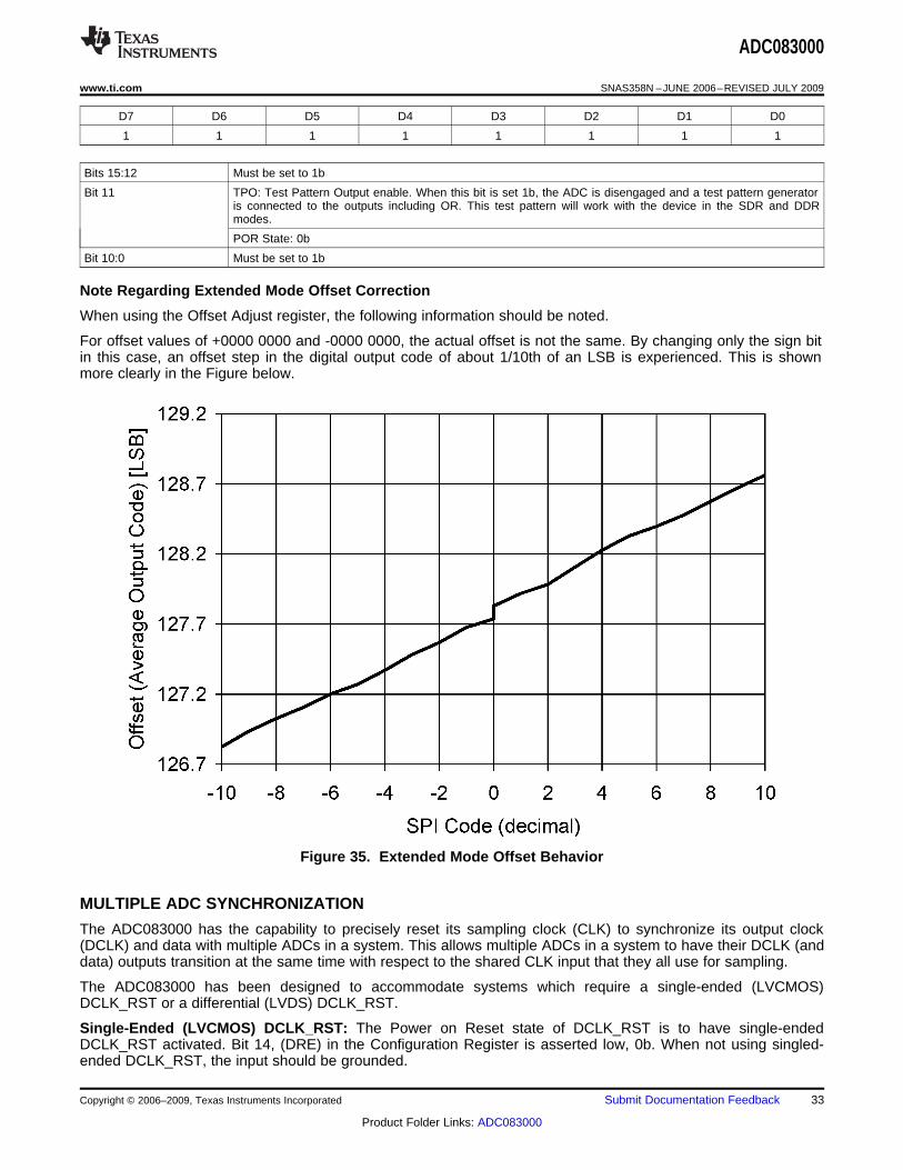
Note Regarding Extended Mode Offset Correction
When using the Offset Adjust register, the following information should be noted.
For offset values of +0000 0000 and -0000 0000, the actual offset is not the same. By changing only the sign bitin this case, an offset step in the digital output code of about 1/10th of an LSB is experienced. This is shownmore clearly in the Figure below.
Figure 35. Extended Mode Offset Behavior
MULTIPLE ADC SYNCHRONIZATION
The ADC083000 has the capability to precisely reset its sampling clock (CLK) to synchronize its output clock(DCLK) and data with multiple ADCs in a system. This allows multiple ADCs in a system to have their DCLK (anddata) outputs transition at the same time with respect to the shared CLK input that they all use for sampling.
The ADC083000 has been designed to accommodate systems which require a single-ended (LVCMOS)DCLK_RST or a differential (LVDS) DCLK_RST.
Single-Ended (LVCMOS) DCLK_RST: The Power on Reset state of DCLK_RST is to have single-endedDCLK_RST activated. Bit 14, (DRE) in the Configuration Register is asserted low, 0b. When not using singled-ended DCLK_RST, the input should be grounded.
Copyright © 2006–2009, Texas Instruments Incorporated Submit Documentation Feedback 33
Product Folder Links: ADC083000

ADC083000
SNAS358N –JUNE 2006–REVISED JULY 2009 www.ti.com
Differential (LVDS) DCLK_RST: Activated by asserting bit 14, (DRE) in the configuration register high, 1b.When the differential DCLK_RST is not activated, the inputs should be grounded. Differential DCLK_RST has aninternal 100 ohm termination resistor and should not be AC coupled.
The DCLK_RST signal must observe some timing requirements that are shown in Figure 5, Figure 6 andFigure 7 of the Timing Diagrams. The DCLK_RST pulse must be of a minimum width and its deassertion edgemust observe setup and hold times with respect to the CLK input rising edge. These times are specified in theAC Electrical Characteristics Table.
The DCLK_RST signal can be asserted asynchronous to the input clock. If DCLK_RST is asserted, the DCLKoutput is held in a designated state. The state in which DCLK is held during the reset period is determined by themode of operation (SDR/DDR) and the setting of the Output Edge configuration pin or bit. (Refer to Figure 5,Figure 6 and Figure 7 for the DCLK reset state conditions). Therefore, depending upon when the DCLK_RSTsignal is asserted, there may be a narrow pulse on the DCLK line during this reset event. When the DCLK_RSTsignal is de-asserted in synchronization with the CLK rising edge, the next CLK falling edge synchronizes theDCLK output with those of other ADC083000s in the system. The DCLK output is enabled again after a constantdelay (relative to the input clock frequency) which is equal to the CLK input to DCLK output delay (tSD). Thedevice always exhibits this delay characteristic in normal operation.
If the device is not programmed to allow DCLK to run continuously, DCLK will become inactive during acalibration cycle. Therefore, it is strongly recommended that DCLK only be used as a data capture clock and notas a system clock.
The DCLK_RST pin should NOT be brought high while the calibration process is running (while CalRun is high).Doing so could cause a digital glitch in the digital circuitry, resulting in corruption and invalidation of thecalibration.
ADC TEST PATTERN
To aid in system debug, the ADC083000 has the capability of providing a test pattern at the four output portscompletely independent of the input signal. The test pattern is selected by setting bit-11 (TPO) in the TestPattern Register (address Fh). The test pattern will appear at the digital output about 10 DCLK cycles after thelast write to the Test Pattern Register.
The ADC is disengaged and a test pattern generator is connected to the outputs including OR. Each port is givena unique 8-bit word, alternating between 1's and 0's as described in theTable 11.
Table 11. Test Pattern by Output Port (1)
Time Da Db Dc Dd OR Comments
T0 01h 02h 03h 04h 0
T1 FEh FDh FCh FBh 1
T2 01h 02h 03h 04h 0 Pattern Sequence n
T3 FEh FDh FCh FBh 1
T4 01h 02h 03h 04h 0
T5 01h 02h 03h 04h 0
T6 FEh FDh FCh FBh 1
T7 01h 02h 03h 04h 0 Pattern Sequence n+1
T8 FEh FDh FCh FBh 1
T9 01h 02h 03h 04h 0
T10 01h 02h 03h 04h 0Pattern Sequence n+2
T11 ... ... ... ... ...
(1) The same bit pattern repeats when the test pattern sequence is concatenated.
34 Submit Documentation Feedback Copyright © 2006–2009, Texas Instruments Incorporated
Product Folder Links: ADC083000

ADC083000
www.ti.com SNAS358N –JUNE 2006–REVISED JULY 2009
APPLICATIONS INFORMATION
THE REFERENCE VOLTAGE
The voltage reference for the ADC083000 is derived from a 1.254V bandgap reference, a buffered version ofwhich is made available at pin 31, VBG, for user convenience. This output has an output current capability of±100 μA. This reference voltage should be buffered if more current is required.
The internal bandgap-derived reference voltage has a nominal value of 600 mV or 820 mV, as determined by theFSR pin and described in The Analog Inputs.
There is no provision for the use of an external reference voltage, but the full-scale input voltage can be adjustedthrough a Configuration Register in the Extended Control mode, as explained in NORMAL/EXTENDEDCONTROL.
Differential input signals up to the chosen full-scale level will be digitized to 8 bits. Signal excursions beyond thefull-scale range will be clipped at the output. These large signal excursions will also activate the OR output forthe time that the signal is out of range. See Out Of Range (OR) Indication.
One extra feature of the VBG pin is that it can be used to raise the common mode voltage level of the LVDSoutputs. The output offset voltage (VOS) is typically 800mV when the VBG pin is used as an output or leftunconnected. To raise the LVDS offset voltage to a typical value of 1150mV the VBG pin can be connecteddirectly to the supply rails.
THE ANALOG INPUT
The analog input is a differential one to which the signal source may be a.c. coupled or d.c. coupled. The full-scale input range is selected with the FSR pin to be 600 mVP-P or 820 mVP-P, or can be adjusted to valuesbetween 560 mVP-P and 840 mVP-P in the Extended Control mode through the Serial Interface. For bestperformance, it is recommended that the full-scale range be kept between 595 mVP-P and 805 mVP-P in theExtended Control mode because the internal DAC which sets the full-scale range is not as linear at the ends ofits range.
Table 12 gives the input to output relationship with the FSR pin high when the normal (non-extended) mode isused. With the FSR pin grounded, the millivolt values in Table 12 are reduced to 75% of the values indicated. Inthe Enhanced Control Mode, these values will be determined by the full scale range and offset settings in theControl Registers.
Table 12. DIFFERENTIAL INPUT TO OUTPUT RELATIONSHIP (Non-Extended Control Mode, FSR High)
VIN+ VIN− Output Code
VCM − 205mV VCM + 205mV 0000 0000
VCM − 102.5 mV VCM + 102.5 mV 0100 0000
0111 1111 /VCM VCM 1000 0000
VCM + 102.5 mV VCM −102.5 mV 1100 0000
VCM + 205mV VCM − 205mV 1111 1111
The buffered analog inputs simplify the task of driving these inputs and the RC pole that is generally used atsampling ADC inputs is not required. If it is desired to use an amplifier circuit before the ADC, use care inchoosing an amplifier with adequate noise and distortion performance and adequate gain at the frequencies usedfor the application.
The Input impedance of VIN+ / VIN-in the d.c. coupled mode (VCMO pin not grounded) consists of a precision 100Ωresistor across the inputs and a capacitance from each of these inputs to ground. In the a.c. coupled mode, theinput appears the same except there is also a resistor of 50KΩ between each analog input pin and the on-chipVCMO potential.
When the inputs are a.c. coupled, the VCMO output must be grounded, as shown in Figure 36. This causes theon-chip VCMO voltage to be connected to the inputs through on-chip 50KΩ resistors.
Copyright © 2006–2009, Texas Instruments Incorporated Submit Documentation Feedback 35
Product Folder Links: ADC083000

VIN+50:
Source
VIN-1:2 Balun
Ccouple
Ccouple
100:
ADC083000
VIN+
VIN-
VCMO
ADC083000
Ccouple
Ccouple
ADC083000
SNAS358N –JUNE 2006–REVISED JULY 2009 www.ti.com
Figure 36. Differential Data Input Connection
When the d.c. coupled mode is used, a precise common mode voltage must be provided at the differentialinputs. This common mode voltage should track the VCMO output pin. Note that the VCMO output potential willchange with temperature. The common mode output of the driving device should track this change.
Full-scale distortion performance falls off rapidly as the input common mode voltage deviates from VCMO. This isa direct result of using a very low supply voltage to minimize power. Keep the input common voltage within 50mV of VCMO.
Performance is as good in the d.c. coupled mode as it is in the a.c. coupled mode, provided the input commonmode voltage at both analog inputs remain within 50 mV of VCMO.
Handling Single-Ended Input Signals
There is no provision for the ADC083000 to adequately process single-ended input signals. The best way tohandle single-ended signals is to convert them to differential signals before presenting them to the ADC.
A.C. Coupled Input
The easiest way to accomplish single-ended a.c. input to differential a.c. signal is with an appropriate balun, asshown in Figure 37.
Figure 37. Single-Ended to Differential signal conversion with a balun
Figure 37 is a generic depiction of a single-ended to differential signal conversion using a balun. The circuitryspecific to the balun will depend on the type of balun selected and the overall board layout. It is recommendedthat the system designer contact the manufacturer of the balun they have selected to aid in designing the bestperforming single-ended to differential conversion circuit using that particular balun.
When selecting a balun, it is important to understand the input architecture of the ADC. There are specific balunparameters of which the system designer should be mindful. They should match the impedance of their analogsource to the ADC083000’s on-chip 100Ω differential input termination resistor. The range of this inputtermination resistor is described in the Converter Electrical Characteristics as the specification RIN.
Also, as a result of the ADC architecture, the phase and amplitude balance are important. The lowest possiblephase and amplitude imbalance is desired when selecting a balun. The phase imbalance should be no more than±2.5° and the amplitude imbalance should be limited to less than 1dB at the desired input frequency range.
Finally, when selecting a balun, the VSWR (Voltage Standing Wave Ratio), bandwidth and insertion loss of thebalun should also be considered. The VSWR aids in determining the overall transmission line terminationcapability of the balun when interfacing to the ADC input. The insertion loss should be considered so that thesignal at the balun output is within the specified input range of the ADC as described in the Converter ElectricalCharacteristics as the specification VIN.
36 Submit Documentation Feedback Copyright © 2006–2009, Texas Instruments Incorporated
Product Folder Links: ADC083000

AD
C08
3000
RA
DJ- VIN-
VIN+
VCMO
50:
SignalInput
LMV321
+-
LMH6555RA
DJ+
3.3V
RT2
50:
RT1
50:
RF1
RF2
RG1
RG2
VCM_REF
50:
100:
+-
50:
ADC083000
www.ti.com SNAS358N –JUNE 2006–REVISED JULY 2009
D.C. Coupled Input
When d.c. coupling to the ADC083000 analog inputs is required, single-ended to differential conversion may beeasily accomplished with the LMH6555. An example of this type of circuit is shown in Figure 38. In suchapplications, the LMH6555 performs the task of single-ended to differential conversion while delivering lowdistortion and noise, as well as output balance, that supports the operation of the ADC083000. Connecting theADC083000 VCMO pin to the VCM_REF pin of the LMH6555, through an appropriate buffer, will ensure that thecommon mode input voltage is as needed for optimum performance of the ADC083000. The LMV321 waschosen to buffer VCMO for its low voltage operation and reasonable offset voltage.
Be sure that the current drawn from the VCMO output does not exceed 100 μA.
Figure 38. Example of Servoing the Analog Input with VCMO
In Figure 38, RADJ-and RADJ+ are used to adjust the differential offset that can be measured at the ADC inputsVIN+ / VIN-. An unadjusted positive offset with reference to VIN-greater than |15mV| should be reduced with aresistor in the RADJ-position. Likewise, an unadjusted negative offset with reference to VIN-greater than |15mV|should be reduced with a resistor in the RADJ+ position. Table 13 gives suggested RADJ-and RADJ+ values forvarious unadjusted differential offsets to bring the VIN+ / VIN-offset back to within |15mV|.
Table 13. D.C. Coupled Offset Adjustment
Unadjusted Offset Reading Resistor Value
0mV to 10mV no resistor needed
11mV to 30mV 20.0kΩ31mV to 50mV 10.0kΩ51mV to 70mV 6.81kΩ71mV to 90mV 4.75kΩ91mV to 110mV 3.92kΩ
Out Of Range (OR) Indication
When the conversion result is clipped the Out of Range output is activated such that OR+ goes high and OR-goes low. This output is active as long as accurate data on either or both of the buses would be outside therange of 00h to FFh. During a calibration cycle, the OR output is invalid. Refer to OVERVIEW for more details.
Full-Scale Input Range
As with all A/D Converters, the input range is determined by the value of the ADC's reference voltage. Thereference voltage of the ADC083000 is derived from an internal band-gap reference. In the normal mode, theFSR pin controls the effective reference voltage of the ADC083000 such that the differential full-scale input rangeat the analog inputs is 820 mVP-P with the FSR pin high, or is 600 mVP-P with FSR pin low. In the ExtendedControl Mode, the Full Scale Range can be set anywhere from 560mV to 840mV. Best SNR is obtained withhigher Full Scale Ranges, but better distortion and SFDR are obtained with lower Full Scale Ranges. TheLMH6555 of Figure 38 is suitable for any Full Scale Range.
Copyright © 2006–2009, Texas Instruments Incorporated Submit Documentation Feedback 37
Product Folder Links: ADC083000

CLK+
CLK-
ADC083000
Ccouple
Ccouple
ADC083000
SNAS358N –JUNE 2006–REVISED JULY 2009 www.ti.com
THE SAMPLE CLOCK INPUT
The ADC083000 has a differential LVDS clock input, CLK+ / CLK-, which must be driven with an a.c. coupled,differential clock signal. Although the ADC083000 is tested and its performance is specified with a differential 1.5GHz clock, it typically will function well with input clock frequencies indicated in the Electrical CharacteristicsTable. The clock inputs are internally terminated and biased. The input clock signal must be capacitively coupledto the clock pins as indicated in Figure 39.
Operation up to the sample rates indicated in the Electrical Characteristics Table is typically possible if themaximum ambient temperatures indicated are not exceeded. Operating at higher sample rates than indicated forthe given ambient temperature may result in reduced device reliability and product lifetime. This is because of thehigher power consumption and die temperatures at high sample rates. Important also for reliability is properthermal management . See Thermal Management.
Figure 39. Differential Sample Clock Connection
The differential sample clock line pair should have a characteristic impedance of 100Ω and be terminated at theclock source in that (100Ω) characteristic impedance. The input clock line should be as short and as direct aspossible. The ADC083000 clock input is internally terminated with an untrimmed 100Ω resistor.
Insufficient input clock levels will result in poor dynamic performance. Excessively high input clock levels couldcause a change in the analog input offset voltage. To avoid these problems, keep the input clock level within therange specified in the Electrical Characteristics Table.
The low and high times of the input clock signal can affect the performance of any A/D Converter. TheADC083000 features a duty cycle clock correction circuit which can maintain performance over temperature. TheADC will meet its performance specification if the input clock high and low times are maintained as specified inthe Electrical Characteristics Table.
High speed, high performance ADCs such as the ADC083000 require a very stable input clock signal withminimum phase noise or jitter. ADC jitter requirements are defined by the ADC resolution (number of bits),maximum ADC input frequency and the input signal amplitude relative to the ADC input full scale range. Themaximum jitter (the sum of the jitter from all sources) allowed to prevent a jitter-induced reduction in SNR isfound to be
tJ(MAX) = (VINFSR/VIN(P-P)) x (1/(2(N+1) x π x fIN))
where tJ(MAX) is the rms total of all jitter sources in seconds, VIN(P-P) is the peak-to-peak analog input signal, VINFSRis the full-scale range of the ADC, "N" is the ADC resolution in bits and fIN is the maximum input frequency, inHertz, at the ADC analog input.
Note that the maximum jitter described above is the Route Sum Square, (RSS), of the jitter from all sources,including that in the ADC input clock, that added by the system to the ADC input clock and input signals and thatadded by the ADC itself. Since the effective jitter added by the ADC is beyond user control, the best the user cando is to keep the sum of the externally added input clock jitter and the jitter added by the analog circuitry to theanalog signal to a minimum.
Input clock amplitudes above those specified in the Electrical Characteristics Table may result in increased inputoffset voltage. This would cause the converter to produce an output code other than the expected 128 when bothinput pins are at the same potential.
38 Submit Documentation Feedback Copyright © 2006–2009, Texas Instruments Incorporated
Product Folder Links: ADC083000

ADC083000
www.ti.com SNAS358N –JUNE 2006–REVISED JULY 2009
Manual Sample Clock Phase Adjust
The sample clock phase can be manually adjusted in the Extended Control Mode to accommodate subtle layoutdifferences when synchronizing multiple ADCs. Register addresses Dh and Eh provide extended mode access tofine and coarse adjustments. Use of Low Frequency Sample Clock control, (register Eh; bit-10) is not supportedwhile using manual sample clock phase adjustments.
It should be noted that by just enabling the phase adjust capability (register Eh; bit-15), degradation of dynamicperformance is expected, specifically SFDR. It is intended that very small adjustments are used. Largerincreases in phase adjustments will begin to affect SNR and ultimately ENOB. Therefore, the use of coarsephase adjustment should be minimized in favor of better system design.
Fine Clock Phase Adjust Range Coarse Clock Phase Adjust Range
CONTROL PINS
Six control pins (without the use of the serial interface) provide a wide range of possibilities in the operation ofthe ADC083000 and facilitate its use. These control pins provide Full-Scale Input Range setting, Calibration,Calibration Delay, Output Edge Synchronization choice, LVDS Output Level choice and a Power Down feature.
Full-Scale Input Range Setting
The input full-scale range can be selected to be either 600 mVP-P or 820 mVP-P, as selected with the FSR controlinput (pin 14) in the Normal Mode of operation. In the Extended Control Mode, the input full-scale range may beset to be anywhere from 560 mVP-P to 840 mVP-P. See THE ANALOG INPUT for more information.
Calibration
The ADC083000 calibration must be run to achieve specified performance. The calibration procedure is run uponpower-up and can be run any time on command. The calibration procedure is exactly the same whether there isan input clock present upon power up or if the clock begins some time after application of power. The CalRunoutput indicator is high while a calibration is in progress. Note that the DCLK outputs are not active during acalibration cycle, therefore it is not recommended as a system clock.
Power-On Calibration
Power-on calibration begins after a time delay following the application of power. This time delay is determinedby the setting of CalDly, as described in the Calibration Delay Section, below.
The calibration process will be not be performed if the CAL pin is high at power up. In this case, the calibrationcycle will not begin until the on-command calibration conditions are met. The ADC083000 will function with theCAL pin held high at power up, but no calibration will be done and performance will be impaired. A manualcalibration, however, may be performed after powering up with the CAL pin high. See On-Command Calibration.
The internal power-on calibration circuitry comes up in an unknown logic state. If the input clock is not running atpower up and the power on calibration circuitry is active, it will hold the analog circuitry in power down and thepower consumption will typically be less than 25 mW. The power consumption will be normal after the clockstarts.
Copyright © 2006–2009, Texas Instruments Incorporated Submit Documentation Feedback 39
Product Folder Links: ADC083000

ADC083000
SNAS358N –JUNE 2006–REVISED JULY 2009 www.ti.com
On-Command Calibration
To initiate an on-command calibration, bring the CAL pin high for a minimum of 80 input clock cycles after it hasbeen low for a minimum of 80 input clock cycles. Holding the CAL pin high upon power up will prevent executionof power-on calibration until the CAL pin is low for a minimum of 80 input clock cycles, then brought high for aminimum of another 80 input clock cycles. The calibration cycle will begin 80 input clock cycles after the CAL pinis thus brought high. The CalRun signal should be monitored to determine when the calibration cycle hascompleted.
The minimum 80 input clock cycle sequences are required to ensure that random noise does not cause acalibration to begin when it is not desired. As mentioned in OVERVIEW for best performance, a calibrationshould be performed 20 seconds or more after power up and repeated when the operating temperature changessignificantly relative to the specific system design performance requirements. ENOB changes slightly withincreasing junction temperature and can be easily corrected by performing an on-command calibration.
Considerations for a continuous DCLK and proper CalRun operation:• During a Power-On calibration cycle, both the ADC and the input termination resistor are calibrated. Because
dynamic performance changes slightly with junction temperature, an On-Command calibration can beexecuted to bring the performance of the ADC in line. By default, On-Command calibration includescalibrating the input termination resistance and the ADC. However, since the input termination resistancechanges only marginally with temperature, the user has the option to disable the input termination resistortrim (address: 1h, bit: 13, set to 1b), which will specify that the DCLK is continuously present at the outputduring calibration. The Resistor Trim Disable can be programmed in the Configuration Register (address: 1h,bit 13) when in the Extended Control mode. Refer to REGISTER DESCRIPTION for register programminginformation.
• When an on-command calibration is requested while using the Aperture Adjust Circuitry through the ExtendedControl Mode registers, we recommend that the Resistor Trim Disable bit be set (address: 1h, bit: 13, set to1b). This allows continuous operation of all clocks in the ADC including DCLK and proper operation of theCalRun output. The Aperture Adjust Circuitry control is resident in the Extended Control Mode registers(addresses: Dh and Eh). Refer to REGISTER DESCRIPTION for register programming information.
Calibration Delay
The CalDly input (pin 127) is used to select one of two delay times after the application of power to the start ofcalibration, as described in Calibration. The calibration delay values allow the power supply to come up andstabilize before calibration takes place. With no delay or insufficient delay, calibration would begin before thepower supply is stabilized at its operating value and result in non-optimal calibration coefficients. If the PD pin ishigh upon power-up, the calibration delay counter will be disabled until the PD pin is brought low. Therefore,holding the PD pin high during power up will further delay the start of the power-up calibration cycle. The bestsetting of the CalDly pin depends upon the power-on settling time of the power supply.
Note that the calibration delay selection is not possible in the Extended Control mode and the short delay time isused.
Output Edge Synchronization
DCLK signals are available to help latch the converter output data into external circuitry. The output data can besynchronized with either edge of these DCLK signals. That is, the output data transition can be set to occur witheither the rising edge or the falling edge of the DCLK signal, so that either edge of that DCLK signal can be usedto latch the output data into the receiving circuit.
When OutEdge (pin 4) is high, the output data is synchronized with (changes with) the rising edge of the DCLK+(pin 82). When OutEdge is low, the output data is synchronized with the falling edge of DCLK+.
At the very high speeds of which the ADC083000 is capable, slight differences in the lengths of the DCLK anddata lines can mean the difference between successful and erroneous data capture. The OutEdge pin is used tocapture data on the DCLK edge that best suits the application circuit and layout.
LVDS Output Level Control
The output level can be set to one of two levels with OutV (pin3). The strength of the output drivers is greaterwith OutV high. With OutV low there is less power consumption in the output drivers, but the lower output levelmeans decreased noise immunity.
40 Submit Documentation Feedback Copyright © 2006–2009, Texas Instruments Incorporated
Product Folder Links: ADC083000

ADC083000
www.ti.com SNAS358N –JUNE 2006–REVISED JULY 2009
For short LVDS lines and low noise systems, satisfactory performance may be realized with the OutV input low.If the LVDS lines are long and/or the system in which the ADC083000 is used is noisy, it may be necessary to tiethe OutV pin high.
Power Down Feature
The Power Down pin (PD) allows the ADC083000 to be entirely powered down. See Power Down for details onthe power down feature.
The digital data (+/-) output pins are put into a high impedance state when the PD pin for the respective channelis high. Upon return to normal operation, the pipeline will contain meaningless information and must be flushed.
If the PD input is brought high while a calibration is running, the device will not go into power down until thecalibration sequence is complete. However, if power is applied and PD is already high, the device will not beginthe calibration sequence until the PD input goes low. If a manual calibration is requested while the device ispowered down, the calibration will not begin at all. That is, the manual calibration input is completely ignored inthe power down state.
THE DIGITAL OUTPUTS
The ADC083000 demultiplexes the output data of each of the two ADCs on the die onto two LVDS output buses(total of four buses, two for each ADC). For each of the two converters, the results of successive conversionsstart on the falling edges of the CLK+ pin and are available on one of the two LVDS buses. The results ofconversions that start on the rising edges of the CLK+ pin are available on the other LVDS bus. This means thatthe word rate at each LVDS bus is 1/2 the ADC083000 input clock rate and the two buses must be multiplexed toobtain the entire 3 GSPS conversion result.
Since the minimum recommended input clock rate for this device is 500 MHz, the sampling rate can be reducedto as low as 1 GSPS by using the results available on all four LVDS busses. The effective sampling rate can bereduced to as low as 250 MSPS by decimating the data by using one bus and a 500MHz clock.
There is one LVDS output clock pair (DCLK+/-) available for use to latch the LVDS outputs on all buses. Whetherthe data is sent at the rising or falling edge of DCLK is determined by the sense of the OutEdge pin, as describedin Output Edge Synchronization.
DDR (Double Data Rate) clocking can also be used. In this mode a word of data is presented with each edge ofDCLK, reducing the DCLK frequency to 1/4 the input clock frequency. When the device is in DDR mode, registeraddress 1h, bit 8 must be set to 0b. See the Timing Diagram section for details.
The OutV pin is used to set the LVDS differential output levels. See LVDS Output Level Control.
The output format is Offset Binary. Accordingly, a full-scale input level with VIN+ positive with respect to VIN− willproduce an output code of all ones, a full-scale input level with VIN− positive with respect to VIN+ will produce anoutput code of all zeros and when VIN+ and VIN− are equal, the output code will be 128.
POWER CONSIDERATIONS
A/D converters draw sufficient transient current to corrupt their own power supplies if not adequately bypassed. A33 µF capacitor should be placed within an inch (2.5 cm) of the A/D converter power pins. A 0.1 µF capacitorshould be placed as close as possible to each VA pin, preferably within one-half centimeter. Leadless chipcapacitors are preferred because they have low lead inductance.
The VA and VDR supply pins should be isolated from each other to prevent any digital noise from being coupledinto the analog portions of the ADC. A ferrite choke, such as the JW Miller FB20009-3B, is recommendedbetween these supply lines when a common source is used for them.
As is the case with all high speed converters, the ADC083000 should be assumed to have little power supplynoise rejection. Any power supply used for digital circuitry in a system where a lot of digital power is beingconsumed should not be used to supply power to the ADC083000. The ADC supplies should be the same supplyused for other analog circuitry, if not a dedicated supply.
Copyright © 2006–2009, Texas Instruments Incorporated Submit Documentation Feedback 41
Product Folder Links: ADC083000
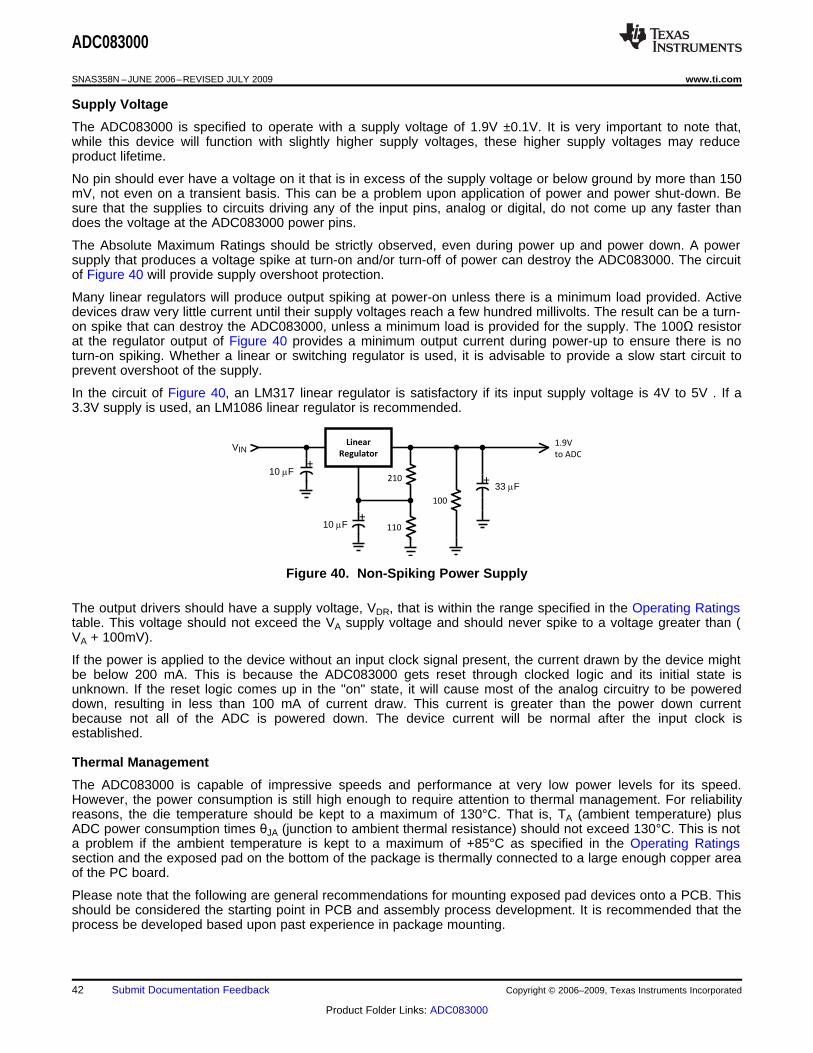
Linear
Regulator
210
110
100
+10 PF
+10 PF
VIN1.9V
to ADC
+33 PF
ADC083000
SNAS358N –JUNE 2006–REVISED JULY 2009 www.ti.com
Supply Voltage
The ADC083000 is specified to operate with a supply voltage of 1.9V ±0.1V. It is very important to note that,while this device will function with slightly higher supply voltages, these higher supply voltages may reduceproduct lifetime.
No pin should ever have a voltage on it that is in excess of the supply voltage or below ground by more than 150mV, not even on a transient basis. This can be a problem upon application of power and power shut-down. Besure that the supplies to circuits driving any of the input pins, analog or digital, do not come up any faster thandoes the voltage at the ADC083000 power pins.
The Absolute Maximum Ratings should be strictly observed, even during power up and power down. A powersupply that produces a voltage spike at turn-on and/or turn-off of power can destroy the ADC083000. The circuitof Figure 40 will provide supply overshoot protection.
Many linear regulators will produce output spiking at power-on unless there is a minimum load provided. Activedevices draw very little current until their supply voltages reach a few hundred millivolts. The result can be a turn-on spike that can destroy the ADC083000, unless a minimum load is provided for the supply. The 100Ω resistorat the regulator output of Figure 40 provides a minimum output current during power-up to ensure there is noturn-on spiking. Whether a linear or switching regulator is used, it is advisable to provide a slow start circuit toprevent overshoot of the supply.
In the circuit of Figure 40, an LM317 linear regulator is satisfactory if its input supply voltage is 4V to 5V . If a3.3V supply is used, an LM1086 linear regulator is recommended.
Figure 40. Non-Spiking Power Supply
The output drivers should have a supply voltage, VDR, that is within the range specified in the Operating Ratingstable. This voltage should not exceed the VA supply voltage and should never spike to a voltage greater than (VA + 100mV).
If the power is applied to the device without an input clock signal present, the current drawn by the device mightbe below 200 mA. This is because the ADC083000 gets reset through clocked logic and its initial state isunknown. If the reset logic comes up in the "on" state, it will cause most of the analog circuitry to be powereddown, resulting in less than 100 mA of current draw. This current is greater than the power down currentbecause not all of the ADC is powered down. The device current will be normal after the input clock isestablished.
Thermal Management
The ADC083000 is capable of impressive speeds and performance at very low power levels for its speed.However, the power consumption is still high enough to require attention to thermal management. For reliabilityreasons, the die temperature should be kept to a maximum of 130°C. That is, TA (ambient temperature) plusADC power consumption times θJA (junction to ambient thermal resistance) should not exceed 130°C. This is nota problem if the ambient temperature is kept to a maximum of +85°C as specified in the Operating Ratingssection and the exposed pad on the bottom of the package is thermally connected to a large enough copper areaof the PC board.
Please note that the following are general recommendations for mounting exposed pad devices onto a PCB. Thisshould be considered the starting point in PCB and assembly process development. It is recommended that theprocess be developed based upon past experience in package mounting.
42 Submit Documentation Feedback Copyright © 2006–2009, Texas Instruments Incorporated
Product Folder Links: ADC083000

0.33 mm, typ
0.25 mm, typ
1.2 mm, typ
5.0 mm, min
ADC083000
www.ti.com SNAS358N –JUNE 2006–REVISED JULY 2009
The package of the ADC083000 has an exposed pad on its back that provides the primary heat removal path aswell as excellent electrical grounding to the printed circuit board. The land pattern design for lead attachment tothe PCB should be the same as for a conventional HLQFP, but the exposed pad must be attached to the boardto remove the maximum amount of heat from the package, as well as to ensure best product parametricperformance.
To maximize the removal of heat from the package, a thermal land pattern must be incorporated on the PCboard within the footprint of the package. The exposed pad of the device must be soldered down to ensureadequate heat conduction out of the package. The land pattern for this exposed pad should be at least as largeas the 5 x 5 mm of the exposed pad of the package and be located such that the exposed pad of the device isentirely over that thermal land pattern. This thermal land pattern should be electrically connected to ground. Aclearance of at least 0.5 mm should separate this land pattern from the mounting pads for the package pins.
Figure 41. Recommended Package Land Pattern
Since a large aperture opening may result in poor release, the aperture opening should be subdivided into anarray of smaller openings, similar to the land pattern of Figure 41.
To minimize junction temperature, it is recommended that a simple heat sink be built into the PCB. This is doneby including a copper area of about 2 square inches (6.5 square cm) on the opposite side of the PCB. Thiscopper area may be plated or solder coated to prevent corrosion, but should not have a conformal coating, whichcould provide some thermal insulation. Thermal vias should be used to connect these top and bottom copperareas. These thermal vias act as "heat pipes" to carry the thermal energy from the device side of the board to theopposite side of the board where it can be more effectively dissipated. The use of 9 to 16 thermal vias isrecommended.
The thermal vias should be placed on a 1.2 mm grid spacing and have a diameter of 0.30 to 0.33 mm. Thesevias should be barrel plated to avoid solder wicking into the vias during the soldering process as this wickingcould cause voids in the solder between the package exposed pad and the thermal land on the PCB. Such voidscould increase the thermal resistance between the device and the thermal land on the board, which would causethe device to run hotter.
If it is desired to monitor die temperature, a temperature sensor may be mounted on the heat sink area of theboard near the thermal vias. Allow for a thermal gradient between the temperature sensor and the ADC083000die of θJ-PAD times typical power consumption = 2.8 x 1.9 = 5.3°C. Allowing for 6.3°C, including some margin fortemperature drop from the pad to the temperature sensor, then, would mean that maintaining a maximum padtemperature reading of 123.7°C will ensure that the die temperature does not exceed 130°C, assuming that theexposed pad of the ADC083000 is properly soldered down and the thermal vias are adequate. (The inaccuracyof the temperature sensor is additional to the above calculation).
LAYOUT AND GROUNDING
Proper grounding and proper routing of all signals are essential to ensure accurate conversion. A single groundplane should be used, instead of splitting the ground plane into analog and digital areas.
Copyright © 2006–2009, Texas Instruments Incorporated Submit Documentation Feedback 43
Product Folder Links: ADC083000

ADC083000
SNAS358N –JUNE 2006–REVISED JULY 2009 www.ti.com
Since digital switching transients are composed largely of high frequency components, the skin effect tells us thattotal ground plane copper weight will have little effect upon the logic-generated noise. Total surface area is moreimportant than is total ground plane volume. Coupling between the typically noisy digital circuitry and thesensitive analog circuitry can lead to poor performance that may seem impossible to isolate and remedy. Thesolution is to keep the analog circuitry well separated from the digital circuitry.
High power digital components should not be located on or near any linear component or power supply trace orplane that services analog or mixed signal components as the resulting common return current path could causefluctuation in the analog input “ground” return of the ADC, causing excessive noise in the conversion result.
Generally, we assume that analog and digital lines should cross each other at 90° to avoid getting digital noiseinto the analog path. In high frequency systems, however, avoid crossing analog and digital lines altogether. Theinput clock lines should be isolated from ALL other lines, analog AND digital. The generally accepted 90°crossing should be avoided as even a little coupling can cause problems at high frequencies. Best performanceat high frequencies is obtained with a straight signal path.
The analog input should be isolated from noisy signal traces to avoid coupling of spurious signals into the input.This is especially important with the low level drive required of the ADC083000. Any external component (e.g., afilter capacitor) connected between the converter's input and ground should be connected to a very clean point inthe analog ground plane. All analog circuitry (input amplifiers, filters, etc.) should be separated from any digitalcomponents.
DYNAMIC PERFORMANCE
The ADC083000 is a.c. tested and its dynamic performance is specified. To meet the published specificationsand avoid jitter-induced noise, the clock source driving the CLK input must exhibit low rms jitter. The allowablejitter is a function of the input frequency and the input signal level, as described in THE SAMPLE CLOCK INPUT.
It is good practice to keep the ADC input clock line as short as possible, to keep it well away from any othersignals and to treat it as a transmission line. Other signals can introduce jitter into the input clock signal. Theclock signal can also introduce noise into the analog path if not isolated from that path.
Best dynamic performance is obtained when the exposed pad at the back of the package has a good connectionto ground. This is because this path from the die to ground is a lower impedance than offered by the packagepins.
USING THE SERIAL INTERFACE
The ADC083000 may be operated in the non-extended control (non-Serial Interface) mode or in the extendedcontrol mode. Table 14 and Table 15 describe the functions of pins 3, 4, 14 and 127 in the non-extended controlmode and the extended control mode, respectively.
Non-Extended Control Mode Operation
Non-extended control mode operation means that the Serial Interface is not active and all controllable functionsare controlled with various pin settings. That is, the output voltage, full-scale range and output edge selectionsare all controlled with pin settings. The non-extended control mode is used by setting pin 14 high or low, asopposed to letting it float. Table 14 indicates the pin functions of the ADC083000 in the non-extended controlmode.
Table 14. Non-Extended Control Mode Operation (Pin 14 High or Low)
Pin Low High Floating
3 0.52 VP-P Output 0.68 VP-P Output n/a
4 OutEdge = Neg OutEdge = Pos DDR
14 600 mVP-P input range 820 mVP-P input range Extended Control Mode
127 CalDly Low CalDly High Serial Interface Enable
44 Submit Documentation Feedback Copyright © 2006–2009, Texas Instruments Incorporated
Product Folder Links: ADC083000

ADC083000
www.ti.com SNAS358N –JUNE 2006–REVISED JULY 2009
Pin 3 can be either high or low in the non-extended control mode. Pin 14 must not be left floating to select thismode. See NORMAL/EXTENDED CONTROL for more information.
Pin 4 can be high or low or can be left floating in the non-extended control mode. In the non-extended controlmode, pin 4 high or low defines the edge at which the output data transitions. See NORMAL/EXTENDEDCONTROL for more information. If this pin is floating, the output clock (DCLK) is a DDR (Double Data Rate)clock (see Double Data Rate) and the output edge synchronization is irrelevant since data is clocked out on bothDCLK edges.
Pin 127, if it is high or low in the non-extended control mode, sets the calibration delay. If pin 127 is floating, thecalibration delay is the same as it would be with this pin low and this pin acts as the enable pin for the serialinterface input.
Table 15. Extended Control Mode Operation (Pin 14 Floating)
Pin Function
3 SCLK (Serial Clock)
4 SDATA (Serial Data)
127 SCS (Serial Interface Chip Select)
COMMON APPLICATION PITFALLS
Failure to write all register locations when using extended control mode. When using the serial interface, allsix address locations must be written at least once with the default or desired values before calibration andsubsequent use of the ADC.
Driving the inputs (analog or digital) beyond the power supply rails. For device reliability, no input should gomore than 150 mV below the ground pins or 150 mV above the supply pins. Exceeding these limits on even atransient basis may not only cause faulty or erratic operation, but may impair device reliability. It is notuncommon for high speed digital circuits to exhibit undershoot that goes more than a volt below ground.Controlling the impedance of high speed lines and terminating these lines in their characteristic impedanceshould control overshoot.
Care should be taken not to overdrive the inputs of the ADC083000. Such practice may lead to conversioninaccuracies and even to device damage.
Incorrect analog input common mode voltage in the d.c. coupled mode. As discussed in The Analog Inputsand THE ANALOG INPUT, the Input common mode voltage must remain within 50 mV of the VCMO output ,which has a variability with temperature that must also be tracked. Distortion performance will be degraded if theinput common mode voltage is more than 50 mV from VCMO .
Using an inadequate amplifier to drive the analog input. Use care when choosing a high frequency amplifierto drive the ADC083000 as many high speed amplifiers will have higher distortion than will the ADC083000,resulting in overall system performance degradation.
Driving the VBG pin to change the reference voltage. As mentioned in THE REFERENCE VOLTAGE, thereference voltage is intended to be fixed to provide one of two different full-scale values (600 mVP-P and 820mVP-P). Over driving this pin will not change the full scale value, but can be used to change the LVDS commonmode voltage from 0.8V to 1.2V by tying the VBG pin to VA.
Driving the clock input with an excessively high level signal. The ADC input clock level should not exceedthe level described in the Operating Ratings Table or the input offset could change.
Inadequate input clock levels. As described in THE SAMPLE CLOCK INPUT, insufficient input clock levels canresult in poor performance. Excessive input clock levels could result in the introduction of an input offset.
Using a clock source with excessive jitter, using an excessively long input clock signal trace, or havingother signals coupled to the input clock signal trace. This will cause the sampling interval to vary, causingexcessive output noise and a reduction in SNR performance.
Failure to provide adequate heat removal. As described in Thermal Management, it is important to provideadequate heat removal to ensure device reliability. This can be done either with adequate air flow or the use of asimple heat sink built into the board. The backside pad should be grounded for best performance.
Copyright © 2006–2009, Texas Instruments Incorporated Submit Documentation Feedback 45
Product Folder Links: ADC083000

PACKAGE OPTION ADDENDUM
www.ti.com 11-Mar-2015
Addendum-Page 1
PACKAGING INFORMATION
Orderable Device Status(1)
Package Type PackageDrawing
Pins PackageQty
Eco Plan(2)
Lead/Ball Finish(6)
MSL Peak Temp(3)
Op Temp (°C) Device Marking(4/5)
Samples
ADC083000CIYB/NOPB ACTIVE HLQFP NNB 128 60 Green (RoHS& no Sb/Br)
CU SN Level-3-260C-168 HR -40 to 85 ADC083000CIYB
(1) The marketing status values are defined as follows:ACTIVE: Product device recommended for new designs.LIFEBUY: TI has announced that the device will be discontinued, and a lifetime-buy period is in effect.NRND: Not recommended for new designs. Device is in production to support existing customers, but TI does not recommend using this part in a new design.PREVIEW: Device has been announced but is not in production. Samples may or may not be available.OBSOLETE: TI has discontinued the production of the device.
(2) Eco Plan - The planned eco-friendly classification: Pb-Free (RoHS), Pb-Free (RoHS Exempt), or Green (RoHS & no Sb/Br) - please check http://www.ti.com/productcontent for the latest availabilityinformation and additional product content details.TBD: The Pb-Free/Green conversion plan has not been defined.Pb-Free (RoHS): TI's terms "Lead-Free" or "Pb-Free" mean semiconductor products that are compatible with the current RoHS requirements for all 6 substances, including the requirement thatlead not exceed 0.1% by weight in homogeneous materials. Where designed to be soldered at high temperatures, TI Pb-Free products are suitable for use in specified lead-free processes.Pb-Free (RoHS Exempt): This component has a RoHS exemption for either 1) lead-based flip-chip solder bumps used between the die and package, or 2) lead-based die adhesive used betweenthe die and leadframe. The component is otherwise considered Pb-Free (RoHS compatible) as defined above.Green (RoHS & no Sb/Br): TI defines "Green" to mean Pb-Free (RoHS compatible), and free of Bromine (Br) and Antimony (Sb) based flame retardants (Br or Sb do not exceed 0.1% by weightin homogeneous material)
(3) MSL, Peak Temp. - The Moisture Sensitivity Level rating according to the JEDEC industry standard classifications, and peak solder temperature.
(4) There may be additional marking, which relates to the logo, the lot trace code information, or the environmental category on the device.
(5) Multiple Device Markings will be inside parentheses. Only one Device Marking contained in parentheses and separated by a "~" will appear on a device. If a line is indented then it is a continuationof the previous line and the two combined represent the entire Device Marking for that device.
(6) Lead/Ball Finish - Orderable Devices may have multiple material finish options. Finish options are separated by a vertical ruled line. Lead/Ball Finish values may wrap to two lines if the finishvalue exceeds the maximum column width.
Important Information and Disclaimer:The information provided on this page represents TI's knowledge and belief as of the date that it is provided. TI bases its knowledge and belief on informationprovided by third parties, and makes no representation or warranty as to the accuracy of such information. Efforts are underway to better integrate information from third parties. TI has taken andcontinues to take reasonable steps to provide representative and accurate information but may not have conducted destructive testing or chemical analysis on incoming materials and chemicals.TI and TI suppliers consider certain information to be proprietary, and thus CAS numbers and other limited information may not be available for release.
In no event shall TI's liability arising out of such information exceed the total purchase price of the TI part(s) at issue in this document sold by TI to Customer on an annual basis.

PACKAGE OPTION ADDENDUM
www.ti.com 11-Mar-2015
Addendum-Page 2

MECHANICAL DATA
NNB0128A
www.ti.com
VNX128A (Rev B)

IMPORTANT NOTICE
Texas Instruments Incorporated and its subsidiaries (TI) reserve the right to make corrections, enhancements, improvements and otherchanges to its semiconductor products and services per JESD46, latest issue, and to discontinue any product or service per JESD48, latestissue. Buyers should obtain the latest relevant information before placing orders and should verify that such information is current andcomplete. All semiconductor products (also referred to herein as “components”) are sold subject to TI’s terms and conditions of salesupplied at the time of order acknowledgment.TI warrants performance of its components to the specifications applicable at the time of sale, in accordance with the warranty in TI’s termsand conditions of sale of semiconductor products. Testing and other quality control techniques are used to the extent TI deems necessaryto support this warranty. Except where mandated by applicable law, testing of all parameters of each component is not necessarilyperformed.TI assumes no liability for applications assistance or the design of Buyers’ products. Buyers are responsible for their products andapplications using TI components. To minimize the risks associated with Buyers’ products and applications, Buyers should provideadequate design and operating safeguards.TI does not warrant or represent that any license, either express or implied, is granted under any patent right, copyright, mask work right, orother intellectual property right relating to any combination, machine, or process in which TI components or services are used. Informationpublished by TI regarding third-party products or services does not constitute a license to use such products or services or a warranty orendorsement thereof. Use of such information may require a license from a third party under the patents or other intellectual property of thethird party, or a license from TI under the patents or other intellectual property of TI.Reproduction of significant portions of TI information in TI data books or data sheets is permissible only if reproduction is without alterationand is accompanied by all associated warranties, conditions, limitations, and notices. TI is not responsible or liable for such altereddocumentation. Information of third parties may be subject to additional restrictions.Resale of TI components or services with statements different from or beyond the parameters stated by TI for that component or servicevoids all express and any implied warranties for the associated TI component or service and is an unfair and deceptive business practice.TI is not responsible or liable for any such statements.Buyer acknowledges and agrees that it is solely responsible for compliance with all legal, regulatory and safety-related requirementsconcerning its products, and any use of TI components in its applications, notwithstanding any applications-related information or supportthat may be provided by TI. Buyer represents and agrees that it has all the necessary expertise to create and implement safeguards whichanticipate dangerous consequences of failures, monitor failures and their consequences, lessen the likelihood of failures that might causeharm and take appropriate remedial actions. Buyer will fully indemnify TI and its representatives against any damages arising out of the useof any TI components in safety-critical applications.In some cases, TI components may be promoted specifically to facilitate safety-related applications. With such components, TI’s goal is tohelp enable customers to design and create their own end-product solutions that meet applicable functional safety standards andrequirements. Nonetheless, such components are subject to these terms.No TI components are authorized for use in FDA Class III (or similar life-critical medical equipment) unless authorized officers of the partieshave executed a special agreement specifically governing such use.Only those TI components which TI has specifically designated as military grade or “enhanced plastic” are designed and intended for use inmilitary/aerospace applications or environments. Buyer acknowledges and agrees that any military or aerospace use of TI componentswhich have not been so designated is solely at the Buyer's risk, and that Buyer is solely responsible for compliance with all legal andregulatory requirements in connection with such use.TI has specifically designated certain components as meeting ISO/TS16949 requirements, mainly for automotive use. In any case of use ofnon-designated products, TI will not be responsible for any failure to meet ISO/TS16949.
Products ApplicationsAudio www.ti.com/audio Automotive and Transportation www.ti.com/automotiveAmplifiers amplifier.ti.com Communications and Telecom www.ti.com/communicationsData Converters dataconverter.ti.com Computers and Peripherals www.ti.com/computersDLP® Products www.dlp.com Consumer Electronics www.ti.com/consumer-appsDSP dsp.ti.com Energy and Lighting www.ti.com/energyClocks and Timers www.ti.com/clocks Industrial www.ti.com/industrialInterface interface.ti.com Medical www.ti.com/medicalLogic logic.ti.com Security www.ti.com/securityPower Mgmt power.ti.com Space, Avionics and Defense www.ti.com/space-avionics-defenseMicrocontrollers microcontroller.ti.com Video and Imaging www.ti.com/videoRFID www.ti-rfid.comOMAP Applications Processors www.ti.com/omap TI E2E Community e2e.ti.comWireless Connectivity www.ti.com/wirelessconnectivity
Mailing Address: Texas Instruments, Post Office Box 655303, Dallas, Texas 75265Copyright © 2015, Texas Instruments Incorporated