Embed Size (px)
Citation preview
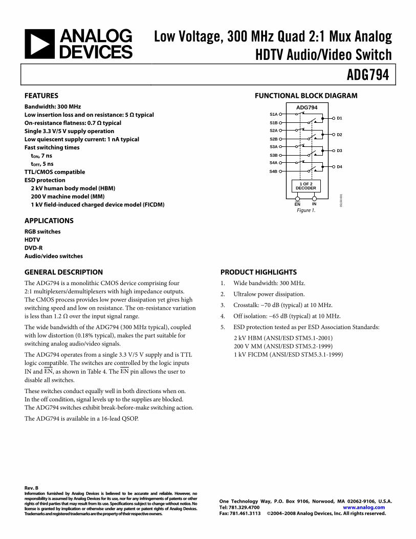
Low Voltage, 300 MHz Quad 2:1 Mux Analog HDTV Audio/Video Switch
ADG794
Rev. B Information furnished by Analog Devices is believed to be accurate and reliable. However, no responsibility is assumed by Analog Devices for its use, nor for any infringements of patents or other rights of third parties that may result from its use. Specifications subject to change without notice. No license is granted by implication or otherwise under any patent or patent rights of Analog Devices. Trademarks and registered trademarks are the property of their respective owners.
One Technology Way, P.O. Box 9106, Norwood, MA 02062-9106, U.S.A.Tel: 781.329.4700 www.analog.com Fax: 781.461.3113 ©2004–2008 Analog Devices, Inc. All rights reserved.
FEATURES Bandwidth: 300 MHz Low insertion loss and on resistance: 5 Ω typical On-resistance flatness: 0.7 Ω typical Single 3.3 V/5 V supply operation Low quiescent supply current: 1 nA typical Fast switching times
tON, 7 ns tOFF, 5 ns
TTL/CMOS compatible ESD protection
2 kV human body model (HBM) 200 V machine model (MM) 1 kV field-induced charged device model (FICDM)
APPLICATIONS RGB switches HDTV DVD-R Audio/video switches
FUNCTIONAL BLOCK DIAGRAM
1 OF 2DECODER
ADG794
EN IN
S1A
S1B
S2A
S2B
S3A
S3B
S4A
S4B
D1
D2
D3
D4
0515
0-00
1
Figure 1.
GENERAL DESCRIPTION The ADG794 is a monolithic CMOS device comprising four 2:1 multiplexers/demultiplexers with high impedance outputs. The CMOS process provides low power dissipation yet gives high switching speed and low on resistance. The on-resistance variation is less than 1.2 Ω over the input signal range.
The wide bandwidth of the ADG794 (300 MHz typical), coupled with low distortion (0.18% typical), makes the part suitable for switching analog audio/video signals.
The ADG794 operates from a single 3.3 V/5 V supply and is TTL logic compatible. The switches are controlled by the logic inputs IN and EN, as shown in Table 4. The EN pin allows the user to disable all switches.
These switches conduct equally well in both directions when on. In the off condition, signal levels up to the supplies are blocked. The ADG794 switches exhibit break-before-make switching action.
The ADG794 is available in a 16-lead QSOP.
PRODUCT HIGHLIGHTS 1. Wide bandwidth: 300 MHz.
2. Ultralow power dissipation.
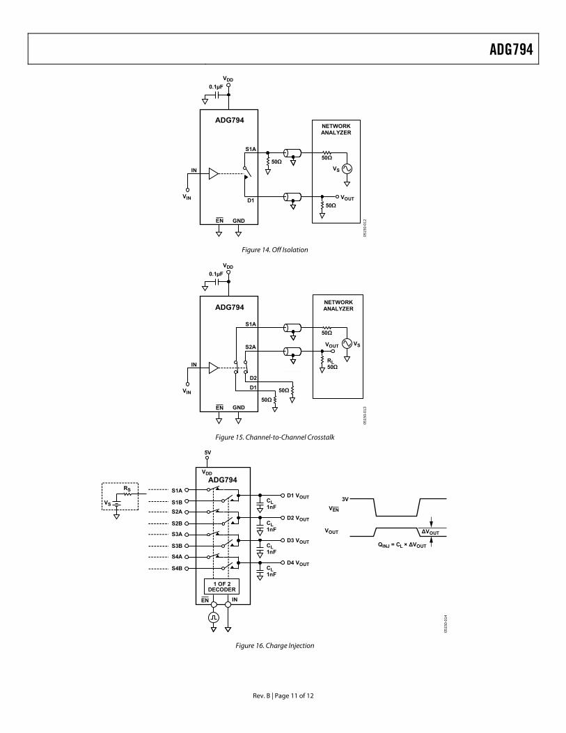
3. Crosstalk: −70 dB (typical) at 10 MHz.
4. Off isolation: −65 dB (typical) at 10 MHz.
5. ESD protection tested as per ESD Association Standards:
2 kV HBM (ANSI/ESD STM5.1-2001) 200 V MM (ANSI/ESD STM5.2-1999) 1 kV FICDM (ANSI/ESD STM5.3.1-1999)
ADG794
Rev. B | Page 2 of 12
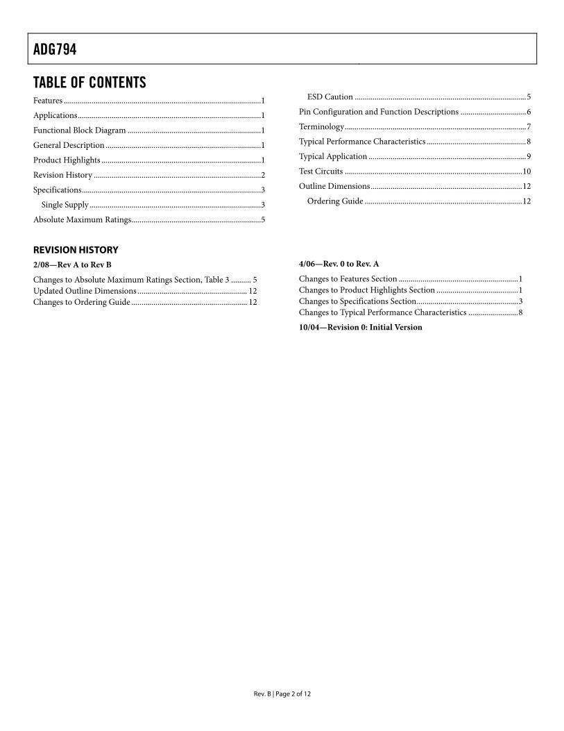
TABLE OF CONTENTS Features ...................................................................................................1 Applications............................................................................................1 Functional Block Diagram ...................................................................1 General Description ..............................................................................1 Product Highlights ................................................................................1 Revision History ....................................................................................2 Specifications..........................................................................................3
Single Supply ......................................................................................3 Absolute Maximum Ratings.................................................................5
ESD Caution ......................................................................................5 Pin Configuration and Function Descriptions .................................6 Terminology...........................................................................................7 Typical Performance Characteristics ..................................................8 Typical Application ...............................................................................9 Test Circuits .........................................................................................10 Outline Dimensions............................................................................12
Ordering Guide ...............................................................................12
REVISION HISTORY2/08—Rev A to Rev B
Changes to Absolute Maximum Ratings Section, Table 3 .......... 5 Updated Outline Dimensions ....................................................... 12 Changes to Ordering Guide .......................................................... 12
4/06—Rev. 0 to Rev. A
Changes to Features Section ............................................................1 Changes to Product Highlights Section .........................................1 Changes to Specifications Section...................................................3 Changes to Typical Performance Characteristics .........................8
10/04—Revision 0: Initial Version
ADG794
Rev. B | Page 3 of 12
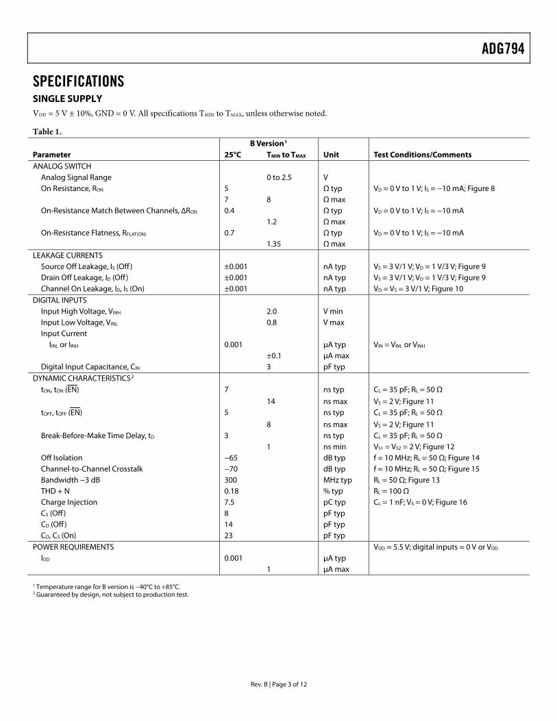
SPECIFICATIONSSINGLE SUPPLY VDD = 5 V ± 10%, GND = 0 V. All specifications TMIN to TMAX, unless otherwise noted.
Table 1. B Version1 Parameter 25°C TMIN to TMAX
Unit Test Conditions/Comments ANALOG SWITCH
Analog Signal Range 0 to 2.5 V On Resistance, RON 5 Ω typ VD = 0 V to 1 V; IS = −10 mA; Figure 8 7 8 Ω max On-Resistance Match Between Channels, ∆RON 0.4 Ω typ VD = 0 V to 1 V; IS = −10 mA 1.2 Ω max On-Resistance Flatness, RFLAT(ON) 0.7 Ω typ VD = 0 V to 1 V; IS = −10 mA 1.35 Ω max
LEAKAGE CURRENTS Source Off Leakage, IS (Off ) ±0.001 nA typ VS = 3 V/1 V; VD = 1 V/3 V; Figure 9Drain Off Leakage, ID (Off ) ±0.001 nA typ VS = 3 V/1 V; VD = 1 V/3 V; Figure 9Channel On Leakage, ID, IS (On) ±0.001 nA typ VD = VS = 3 V/1 V; Figure 10
DIGITAL INPUTS Input High Voltage, VINH 2.0 V min Input Low Voltage, VINL 0.8 V max Input Current
IINL or IINH 0.001 μA typ VIN = VINL or VINH ±0.1 μA max Digital Input Capacitance, CIN 3 pF typ
DYNAMIC CHARACTERISTICS2 tON, tON (EN) 7 ns typ CL = 35 pF; RL = 50 Ω
14 ns max VS = 2 V; Figure 11tOFF, tOFF (EN) 5 ns typ CL = 35 pF; RL = 50 Ω
8 ns max VS = 2 V; Figure 11Break-Before-Make Time Delay, tD 3 ns typ CL = 35 pF; RL = 50 Ω 1 ns min VS1 = VS2 = 2 V; Figure 12Off Isolation −65 dB typ f = 10 MHz; RL = 50 Ω; Figure 14Channel-to-Channel Crosstalk −70 dB typ f = 10 MHz; RL = 50 Ω; Figure 15Bandwidth −3 dB 300 MHz typ RL = 50 Ω; Figure 13THD + N 0.18 % typ RL = 100 Ω Charge Injection 7.5 pC typ CL = 1 nF; VS = 0 V; Figure 16CS (Off ) 8 pF typ CD (Off ) 14 pF typ CD, CS (On) 23 pF typ
POWER REQUIREMENTS VDD = 5.5 V; digital inputs = 0 V or VDD IDD 0.001 μA typ
1 μA max 1 Temperature range for B version is −40°C to +85°C. 2 Guaranteed by design, not subject to production test.
ADG794
Rev. B | Page 4 of 12
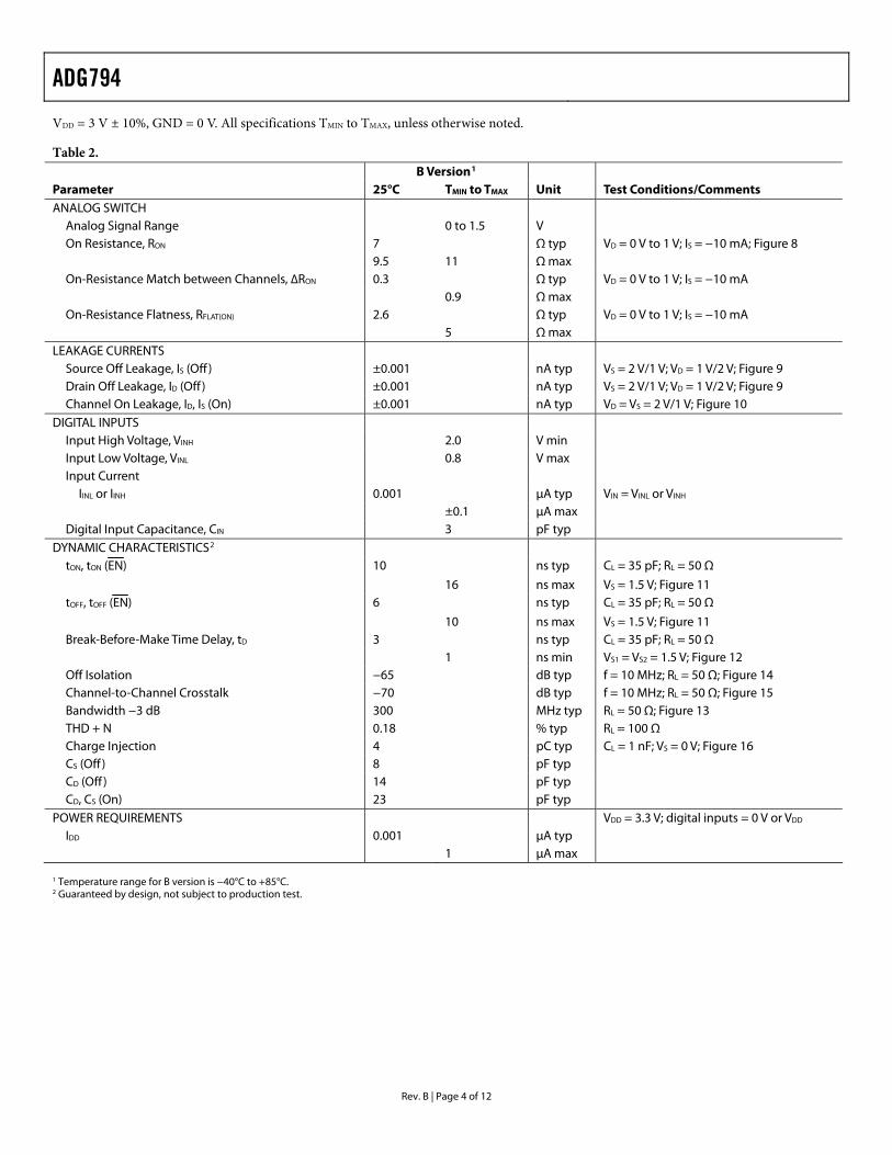
VDD = 3 V ± 10%, GND = 0 V. All specifications TMIN to TMAX, unless otherwise noted.
Table 2. B Version1 Parameter 25°C TMIN to TMAX Unit Test Conditions/Comments ANALOG SWITCH
Analog Signal Range 0 to 1.5 V On Resistance, RON 7 Ω typ VD = 0 V to 1 V; IS = −10 mA; Figure 8 9.5 11 Ω max On-Resistance Match between Channels, ∆RON 0.3 Ω typ VD = 0 V to 1 V; IS = −10 mA 0.9 Ω max On-Resistance Flatness, RFLAT(ON) 2.6 Ω typ VD = 0 V to 1 V; IS = −10 mA 5 Ω max
LEAKAGE CURRENTS Source Off Leakage, IS (Off ) ±0.001 nA typ VS = 2 V/1 V; VD = 1 V/2 V; Figure 9Drain Off Leakage, ID (Off ) ±0.001 nA typ VS = 2 V/1 V; VD = 1 V/2 V; Figure 9Channel On Leakage, ID, IS (On) ±0.001 nA typ VD = VS = 2 V/1 V; Figure 10
DIGITAL INPUTS Input High Voltage, VINH 2.0 V min Input Low Voltage, VINL 0.8 V max Input Current
IINL or IINH 0.001 μA typ VIN = VINL or VINH ±0.1 μA max Digital Input Capacitance, CIN 3 pF typ
DYNAMIC CHARACTERISTICS2 tON, tON (EN) 10 ns typ CL = 35 pF; RL = 50 Ω
16 ns max VS = 1.5 V; Figure 11tOFF, tOFF (EN) 6 ns typ CL = 35 pF; RL = 50 Ω
10 ns max VS = 1.5 V; Figure 11Break-Before-Make Time Delay, tD 3 ns typ CL = 35 pF; RL = 50 Ω 1 ns min VS1 = VS2 = 1.5 V; Figure 12Off Isolation −65 dB typ f = 10 MHz; RL = 50 Ω; Figure 14Channel-to-Channel Crosstalk −70 dB typ f = 10 MHz; RL = 50 Ω; Figure 15Bandwidth −3 dB 300 MHz typ RL = 50 Ω; Figure 13THD + N 0.18 % typ RL = 100 Ω Charge Injection 4 pC typ CL = 1 nF; VS = 0 V; Figure 16CS (Off ) 8 pF typ CD (Off ) 14 pF typ CD, CS (On) 23 pF typ
POWER REQUIREMENTS VDD = 3.3 V; digital inputs = 0 V or VDD IDD 0.001 μA typ
1 μA max 1 Temperature range for B version is −40°C to +85°C. 2 Guaranteed by design, not subject to production test.
ADG794
Rev. B | Page 5 of 12
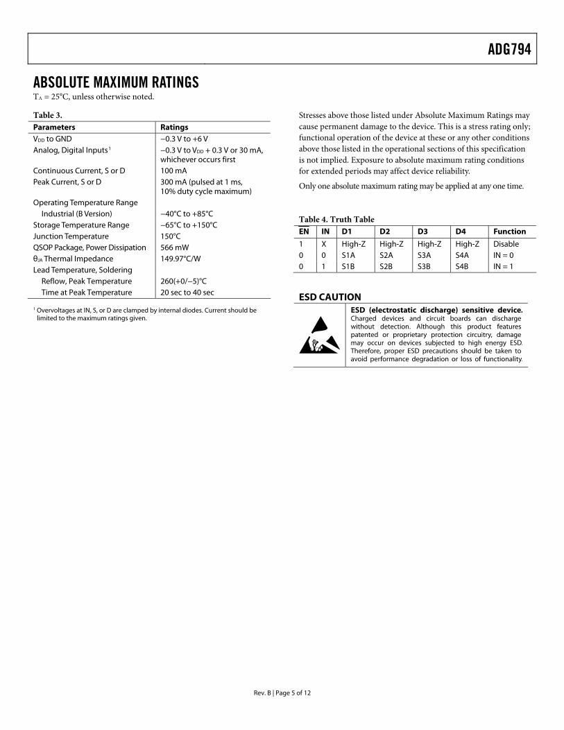
ABSOLUTE MAXIMUM RATINGS TA = 25°C, unless otherwise noted.
Table 3. Parameters Ratings VDD to GND −0.3 V to +6 V Analog, Digital Inputs1 −0.3 V to VDD + 0.3 V or 30 mA,
whichever occurs first Continuous Current, S or D 100 mA Peak Current, S or D 300 mA (pulsed at 1 ms,
10% duty cycle maximum) Operating Temperature Range
Industrial (B Version) −40°C to +85°C Storage Temperature Range −65°C to +150°C Junction Temperature 150°C QSOP Package, Power Dissipation 566 mW θJA Thermal Impedance 149.97°C/W Lead Temperature, Soldering
Reflow, Peak Temperature 260(+0/−5)°C Time at Peak Temperature 20 sec to 40 sec
1 Overvoltages at IN, S, or D are clamped by internal diodes. Current should be
limited to the maximum ratings given.
Stresses above those listed under Absolute Maximum Ratings may cause permanent damage to the device. This is a stress rating only; functional operation of the device at these or any other conditions above those listed in the operational sections of this specification is not implied. Exposure to absolute maximum rating conditions for extended periods may affect device reliability.
Only one absolute maximum rating may be applied at any one time.
Table 4. Truth Table EN IN D1 D2 D3 D4 Function
1 X High-Z High-Z High-Z High-Z Disable 0 0 S1A S2A S3A S4A IN = 0 0 1 S1B S2B S3B S4B IN = 1
ESD CAUTION
ADG794
Rev. B | Page 6 of 12
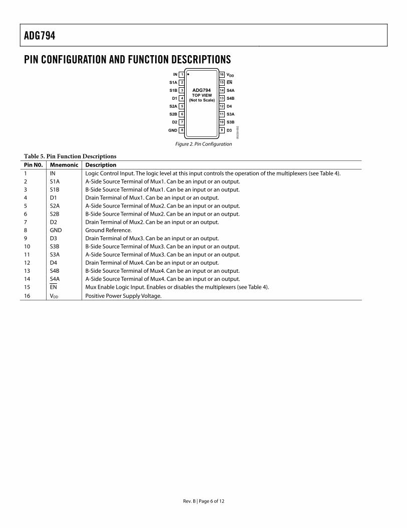
PIN CONFIGURATION AND FUNCTION DESCRIPTIONS 1
2
3
4
5
6
7
8
16
15
14
13
12
11
10
9
S1A
S1B
D1
D2
S2B
S2A
IN
EN
S4A
S4B
S3B
GND D3
S3A
D4
VDD
TOP VIEW(Not to Scale)
ADG794
0515
0-00
2
Figure 2. Pin Configuration
Table 5. Pin Function Descriptions Pin N0. Mnemonic Description 1 IN Logic Control Input. The logic level at this input controls the operation of the multiplexers (see Table 4). 2 S1A A-Side Source Terminal of Mux1. Can be an input or an output. 3 S1B B-Side Source Terminal of Mux1. Can be an input or an output. 4 D1 Drain Terminal of Mux1. Can be an input or an output. 5 S2A A-Side Source Terminal of Mux2. Can be an input or an output. 6 S2B B-Side Source Terminal of Mux2. Can be an input or an output. 7 D2 Drain Terminal of Mux2. Can be an input or an output. 8 GND Ground Reference. 9 D3 Drain Terminal of Mux3. Can be an input or an output. 10 S3B B-Side Source Terminal of Mux3. Can be an input or an output. 11 S3A A-Side Source Terminal of Mux3. Can be an input or an output. 12 D4 Drain Terminal of Mux4. Can be an input or an output. 13 S4B B-Side Source Terminal of Mux4. Can be an input or an output. 14 S4A A-Side Source Terminal of Mux4. Can be an input or an output. 15 EN Mux Enable Logic Input. Enables or disables the multiplexers (see Table 4).
16 VDD Positive Power Supply Voltage.
ADG794
Rev. B | Page 7 of 12
TERMINOLOGY VDD
Most positive power supply potential.
IDD Positive supply current.
GND Ground (0 V) reference.
S Source terminal. Can be either an input or an output.
D Drain terminal. Can be either an input or an output.
IN Logic control input.
VD (VS) Analog voltage on Terminal D and Terminal S.
RON Ohmic resistance between Terminal D and Terminal S.
RFLAT (ON) Flatness is defined as the difference between the maximum and minimum value of on resistance as measured.
ΔRON On-resistance match between any two channels.
IS (Off) Source leakage current with the switch off.
ID (Off) Drain leakage current with the switch off.
ID, IS (On) Channel leakage current with the switch on.
VINL Maximum input voltage for Logic 0.
VINH Minimum input voltage for Logic 1.
IINL (IINH) Input current of the digital input.
CS (Off) Off switch source capacitance. Measured with reference to ground.
CD (Off) Off switch drain capacitance. Measured with reference to ground.
CD, CS (On) On switch capacitance. Measured with reference to ground.
CIN Digital input capacitance.
tON Delay time between the 50% and the 90% points of the digital input and switch on condition.
tOFF Delay time between the 50% and the 90% points of the digital input and switch off condition.
tBBM On or off time measured between the 80% points of both switches when switching from one to another.
Charge Injection A measure of the glitch impulse transferred from the digital input to the analog output during on/off switching.
Off Isolation A measure of unwanted signal coupling through an off switch.
Crosstalk A measure of unwanted signal that is coupled through from one channel to another as a result of parasitic capacitance.
−3 dB Bandwidth The frequency at which the output is attenuated by 3 dB.
On Response The frequency response of the on switch.
Insertion Loss The loss due to the on resistance of the switch.
THD + N The ratio of the harmonic amplitudes plus the noise of a signal to the fundamental.
ADG794
Rev. B | Page 8 of 12
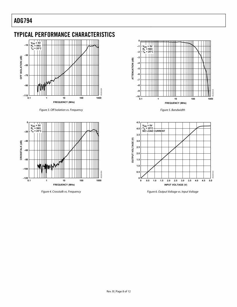
TYPICAL PERFORMANCE CHARACTERISTICS
–110
–90
–70
–50
–30
–10
0.1 100005
150-
003
FREQUENCY (MHz)
OFF
ISO
LATI
ON
(dB
)
1 10 100
VDD = 5VRL = 50ΩTA = 25°C
Figure 3. Off Isolation vs. Frequency
0
–1200.1 1000
0515
0-00
4
FREQUENCY (MHz)
CR
OSS
TALK
(dB
)
1 10 100
–20
–40
–60
–80
–100
VDD = 5VRL = 50ΩTA = 25°C
Figure 4. Crosstalk vs. Frequency
0
–100.1 1000
0515
0-01
5
FREQUENCY (MHz)
ATT
ENU
ATI
ON
(dB
)
1 10 100
–1
–2
–3
–4
–5
–6
–7
–8
–9
VDD = 5VRL = 50ΩTA = 25°C
Figure 5. Bandwidth
4.5
00 5
0515
0-01
6
INPUT VOLTAGE (V)
OU
TPU
T VO
LTA
GE
(V)
.0
4.0
3.5
3.0
2.5
2.0
1.5
1.0
0.5
0.5 1.0 1.5 2.0 2.5 3.0 3.5 4.0 4.5
VDD = 5VTA = 25°CNO LOAD CURRENT
Figure 6. Output Voltage vs. Input Voltage
ADG794
Rev. B | Page 9 of 12
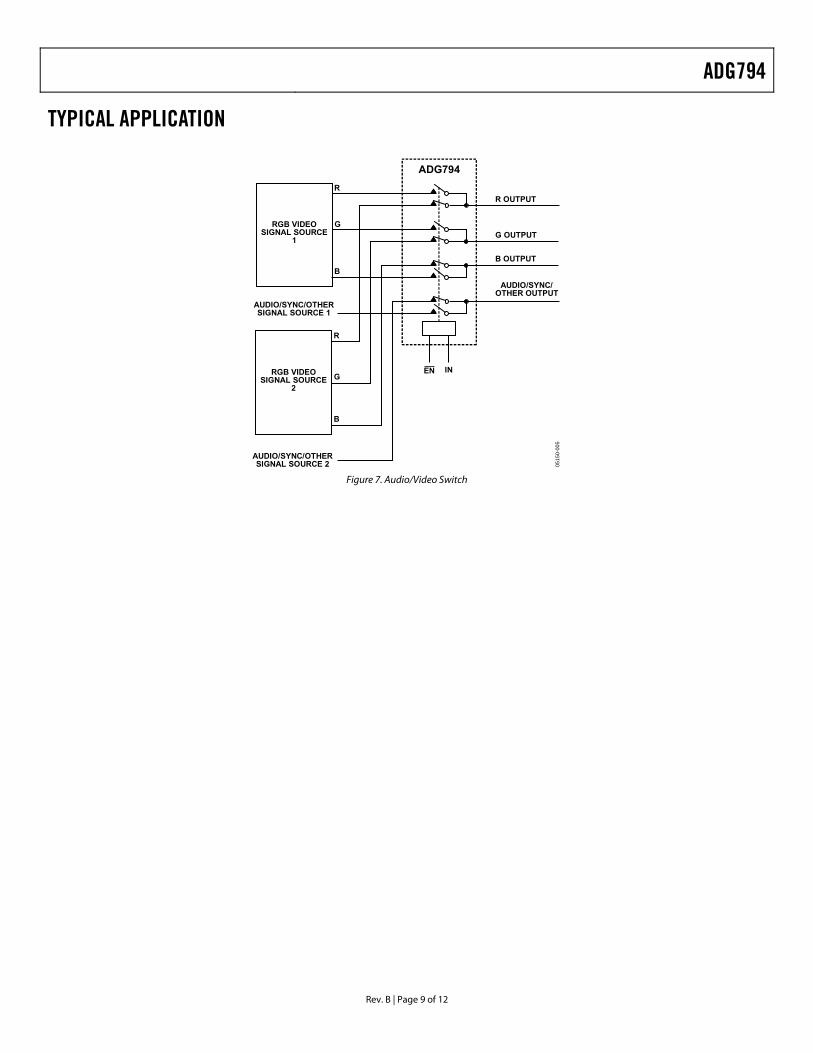
TYPICAL APPLICATION
ADG794R
G
B
RGB VIDEOSIGNAL SOURCE
1
R
G
B
RGB VIDEOSIGNAL SOURCE
2
AUDIO/SYNC/OTHERSIGNAL SOURCE 1
AUDIO/SYNC/OTHERSIGNAL SOURCE 2
EN IN
R OUTPUT
AUDIO/SYNC/OTHER OUTPUT
G OUTPUT
B OUTPUT
0515
0-00
5
Figure 7. Audio/Video Switch
ADG794
Rev. B | Page 10 of 12
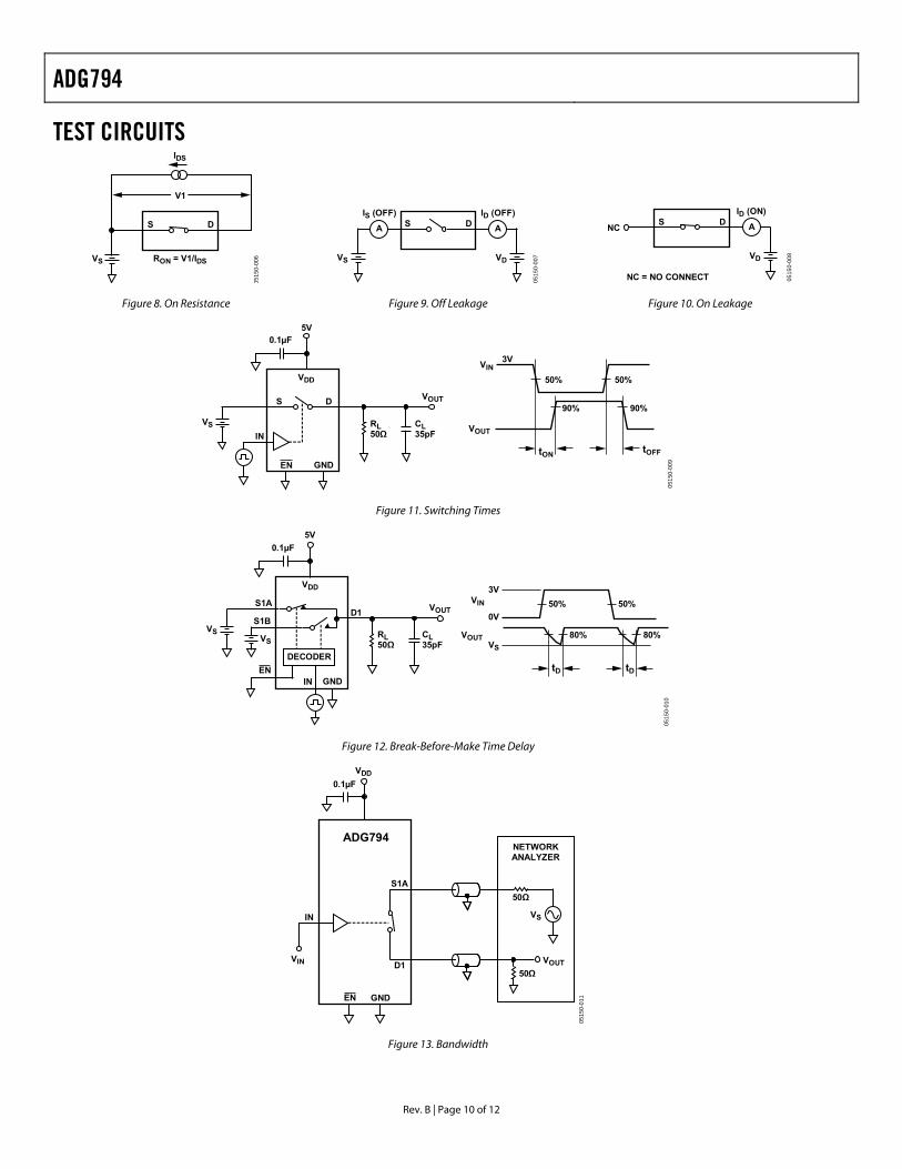
TEST CIRCUITSIDS
V1
S D
VS RON = V1/IDS05
150-
006
S D
VS
A A
VD
IS (OFF) ID (OFF)
0515
0-00
7
S D A
VD
ID (ON)
0515
0-00
8
NC
NC = NO CONNECT
Figure 8. On Resistance Figure 9. Off Leakage Figure 10. On Leakage
0.1µF5V
VSIN
S D
VDD
GND
RL50Ω
CL35pF
VOUT
EN
3V
50% 50%
90% 90%
VIN
VOUT
tON tOFF
0515
0-00
9
Figure 11. Switching Times
0.1µF5V
VS
EN
S1AD1
VDD
GND
RL50Ω
CL35pF
VOUTS1B
DECODER
VS80% 80%
VIN
VOUT
tD tD
50% 50%3V
0V
VS
0515
0-01
0
IN
Figure 12. Break-Before-Make Time Delay
0.1µFVDD
GNDEN
50ΩVOUT
VSIN
D1VIN
S1A
ADG794
50Ω
NETWORKANALYZER
0515
0-01
1
Figure 13. Bandwidth
ADG794
Rev. B | Page 11 of 12
0.1µFVDD
GNDEN
50ΩVOUT
VSIN
D1VIN
S1A
ADG794
50Ω
NETWORKANALYZER
0515
0-01
2
50Ω
Figure 14. Off Isolation
0.1µFVDD
GNDEN
RL50Ω
VOUT VS
IN
D1VIN
S1A
ADG794
50Ω
NETWORKANALYZER
0515
0-01
3
S2A
D2
50Ω50Ω
Figure 15. Channel-to-Channel Crosstalk
5V
EN
S1A
VDD
CL1nF
S1BVEN
VOUT
3V
ΔVOUT
QINJ = CL × ΔVOUT
CL1nF
CL1nF
CL1nF
D1 VOUT
D2 VOUT
D3 VOUT
D4 VOUT
ADG794
1 OF 2DECODER
IN
S2A
S2B
S3A
S3B
S4A
S4B
VS
RS
0515
0-01
4
Figure 16. Charge Injection
ADG794
Rev. B | Page 12 of 12
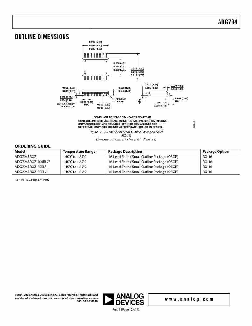
OUTLINE DIMENSIONS
COMPLIANT TO JEDEC STANDARDS MO-137-AB
0128
08-ACONTROLLING DIMENSIONS ARE IN INCHES; MILLIMETERS DIMENSIONS
(IN PARENTHESES) ARE ROUNDED-OFF INCH EQUIVALENTS FORREFERENCE ONLY AND ARE NOT APPROPRIATE FOR USE IN DESIGN.
16 9
81
SEATINGPLANE
0.010 (0.25)0.004 (0.10)
0.012 (0.30)0.008 (0.20)
0.025 (0.64)BSC
0.041 (1.04)REF
0.010 (0.25)0.006 (0.15)
0.050 (1.27)0.016 (0.41)
0.020 (0.51)0.010 (0.25)
8°0°COPLANARITY
0.004 (0.10)
0.065 (1.65)0.049 (1.25)
0.069 (1.75)0.053 (1.35)
0.197 (5.00)0.193 (4.90)0.189 (4.80)
0.158 (4.01)0.154 (3.91)0.150 (3.81) 0.244 (6.20)
0.236 (5.99)0.228 (5.79)
Figure 17. 16-Lead Shrink Small Outline Package [QSOP]
(RQ-16) Dimensions shown in inches and (millimeters)
ORDERING GUIDE Model Temperature Range Package Description Package Option ADG794BRQZ1 −40°C to +85°C 16-Lead Shrink Small Outline Package (QSOP) RQ-16 ADG794BRQZ-500RL71 −40°C to +85°C 16-Lead Shrink Small Outline Package (QSOP) RQ-16 ADG794BRQZ-REEL1 −40°C to +85°C 16-Lead Shrink Small Outline Package (QSOP) RQ-16 ADG794BRQZ-REEL71 −40°C to +85°C 16-Lead Shrink Small Outline Package (QSOP) RQ-16 1 Z = RoHS Compliant Part.
©2004–2008 Analog Devices, Inc. All rights reserved. Trademarks and registered trademarks are the property of their respective owners. D05150-0-2/08(B)