Embed Size (px)
Citation preview
Adhesion and Reliability of Direct Cu Metallization of Through-Package Vias in Glass
Interposers
Timothy Huang, Venky Sundaram, P. Markondeya Raj, Himani Sharma, and Rao Tummala
3D Systems Packaging Research Center
813 Ferst Drive NW
Atlanta, GA 30332-0250
Abstract
Direct metallization of bare glass with copper is required to
reach the full potential low-cost benefit of glass interposers.
However, this poses a fundamental materials challenge
associated with copper-to-glass adhesion. Intermediate
polymer liners on glass have been used by others, adding an
extra material and processing step. In this paper, three
approaches to direct metallization of copper to glass interposers
are explored and reported. Electroless plating, sputtering
followed by electrolytic plating, and sol-gel were investigated
as Cu deposition methods with an emphasis on adhesion and
reliability of copper to bare glass. The adhesion and reliability
performance of films were characterized by tape-testing, peel-
strength measurements, and thermal-shock testing. Based on
these results, individual assessments are made for each
approach and compared with others to assess future directions.
Introduction
The need for high logic-memory bandwidth in both mobile
and high-performance applications with emerging 2.5D and 3D
package architectures has been driving new advances in
interposer and substrate materials. The semiconductor industry
is primarily focusing on Si as the next-generation interposer
material to address the challenges associated with dimensional
instability and coefficient of thermal expansion (CTE)
mismatch with organic packages. Based on recent pioneering
technical advances by Georgia Tech, glass has been
demonstrated as the best next-generation interposer and
package material to meet the high-I/O, high-performance, and
low-cost requirements for advanced packaging [1]. In addition,
because of glass’s matched coefficient of thermal expansion
(CTE) (few ppm/°C) with that of Si IC (2.5 ppm/°C),
thermomechanical reliability is expected to be superior when
compared to organic substrates of much higher CTE (18-22
ppm/°C), where CTE mismatch causes serious reliability
concerns. Compared to organic packages, glass can be
manufactured with a higher density of through-vias and with
higher wiring density and I/Os to the chip because of its Si-like
dimensional stability, and in addition, demonstrating better
electrical performance and lower loss while scalable to large
panels with high manufacturing through-put.
One of the major challenges with glass, however, is its
metallization with copper conductors with sufficient adhesion.
Due to the differences in their chemical structures, most
metallic materials such as Cu do not bond strongly to oxide
networks of silicate glasses. This results in insufficient
adhesion and failure to meet reliability criteria. One approach
that has been demonstrated to circumvent this is to coat both
sides of glass with a polymer film before the glass through
package vias (TPVs) are made. After the creation of vias by
excimer laser ablation, the polymer surface and the roughened-
glass via sidewalls can be metallized by standard electroless
processes [2]. The major disadvantage of this approach is its
limited compatibility with via-formation methods. Glass
manufacturers have recently developed proprietary TPV
formation processes, some of which are not fully compatible
with polymer-coated glass. Direct metallization of copper on
smooth glass surfaces without polymer also provides more
opportunities for lower cost, miniaturization as well as
reliability and electrical performance improvements.
In general, covalent-bonded oxide networks such as glass
bond directly to materials composed of oxides or oxide
interfaces that are stable. Since Cu is composed of metallic-
bonded atoms, some surface modification that results in an
oxide formation can be expected to result in enhanced bonding.
Surface modifications can be physical (e.g., mechanical
interlocking) or chemical, with the latter being ideal. For good
chemical adhesion between bare copper metal and glass,
fundamental adhesion theory states that it is important to have
an intermediate metal oxide interface for strong and lasting
adhesion. Based on this fundamental principle, a process that
enhances chemical bonding through gradual, continuous
material-property changes in the transition from glass to metal
oxide to metal is preferred over mechanical-based methods to
achieve strong adhesion. For example, it is well known that
certain, reactive metals with high oxygen affinity (e.g., Cr, Ti,
Zr, Mg) exhibit strong bonding “directly” to glass by forming
thin oxide layers at the interfaces [3,4]. These oxides are very
stable even at high temperatures and in reducing gas
atmospheres. While standard vacuum deposition techniques
benefit from this approach by depositing an adhesion layer such
as Ti between Cu and glass, new innovations [5,6] are required
to achieve this intermediate “adherence oxide” layer with wet
metallization techniques as described next.
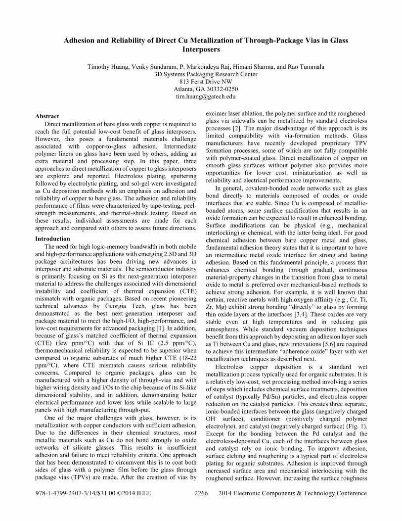
Electroless copper deposition is a standard wet
metallization process typically used for organic substrates. It is
a relatively low-cost, wet processing method involving a series
of steps which includes chemical surface treatments, deposition
of catalyst (typically Pd/Sn) particles, and electroless copper
reduction on the catalyst particles. This creates three separate,
ionic-bonded interfaces between the glass (negatively charged
OH- surface), conditioner (positively charged polymer
electrolyte), and catalyst (negatively charged surface) (Fig. 1).
Except for the bonding between the Pd catalyst and the
electroless-deposited Cu, each of the interfaces between glass
and catalyst rely on ionic bonding. To improve adhesion,
surface etching and roughening is a typical part of electroless
plating for organic substrates. Adhesion is improved through
increased surface area and mechanical interlocking with the
roughened surface. However, increasing the surface roughness
978-1-4799-2407-3/14/$31.00 ©2014 IEEE 2266 2014 Electronic Components & Technology Conference
of the glass-metal interface will result in higher conductor
losses, especially at higher frequencies due to the skin-effect
[7]. Additionally, glass roughening processes are difficult to
control precisely and can introduce flaws or cracks, resulting in
increased risk of mechanical failure. Since chemical, covalent
bonds are not directly made between the Cu and the glass oxide
network, glass surface roughness is mandatory for achieving
sufficient adhesion. To maximize electrical performance and
mechanical integrity, it is therefore of interest to find the
minimum roughness required to achieve sufficient adhesion
through roughening for electroless plating. Companies such as
Atotech, Inc. are pioneering novel surface treatments and
nanoparticle-based copper deposition approaches to achieve
metal-glass adhesion with minimal roughness [5,6].
Figure 1. Schematic of chemical interfaces between
electroless Cu and glass (not to scale).
In the MCM-D (MultiChip Module – Deposition) and flat-
panel display industries, sputtering is a standard metallization
process for ceramic substrates and large panels of bare glass.
High-performance packaging requires thicker metal lines than
what sputtering alone can achieve cost-effectively. The
approach in this paper uses sputtered adhesion (Ti) and seed
(Cu) layers, which are subsequently electroplated at high
deposition rates to reach the necessary Cu thickness. Since
glass/Ti and Ti/Cu are known to be strong interfaces
individually, the glass/Ti/Cu composite structure is also
expected to be strong.
Sol-gel is a common approach to deposit thin films due to
its versatility with available chemistries and its relative
simplicity as a process. In this wet deposition process, a metal-
organic precursor solution (sol) is deposited onto the substrate.
Because of the low viscosity of the solutions, the substrate can
be dip-coated, spin-coated, or sprayed with controlled
thickness to form a three-dimensional network (gel). The film
is then subjected to a temperature high enough to pyrolyze the
organic components, resulting in a three-dimensional network
of the metal oxide. Finally, it is sintered at a higher temperature
to crystallize the film, creating a glass/CuOx/Cu structure.
This paper investigates three approaches to metallize glass
directly, without relying on organic materials that may hinder
subsequent processing: electroless Cu deposition, sputtering
with electrolytic plating, and sol-gel synthesis. For sputtering
and sol-gel, the resulting glass-metal oxide-metal structure is
expected to demonstrate strong adhesion. As the electroless Cu
does not introduce an oxide interface, weaker adhesion is
expected. Based on the results from each of the approaches
described above, individual assessments are made in terms of
potential feasibility and future directions.
Experimental Methods
The three approaches to metallize glass are briefly
described here. The key characterization techniques employed
in this work are also outlined. Smooth and roughened glass-
substrates were provided by Corning, Inc. and Life BioScience,
Inc. Roughened samples were characterized by atomic force
microscopy (Veeco AFM) prior to processing to obtain
roughness (Ra), and ranged from < 1 nm to 0.559 m.
Electroless processes were used to deposit electroless
copper. The electroless-plating steps are substrate cleaning,
conditioning (deposition of polymer electrolyte), catalyst
deposition, catalyst activation, and finally electroless copper
deposition. Triple rinses in water were performed between each
step. Electroless deposition was performed until 0.2 m of Cu
was deposited. Finally, samples were annealed at 155°C for 30
minutes in air. Tape-tests were then performed according to
IPC-TM-650 test standards. For samples which failed the tape-
test, the substrate and peeled interfaces were analyzed by X-ray
photoelectron spectroscopy (XPS) (Thermo K-Alpha XPS) for
the presence of Cu, Si, and C [8].
Sputtering was performed by Tango Systems, Inc. Ti (100
nm) was first deposited as an oxide-forming adhesion layer,
followed by Cu deposition to various thicknesses. Samples
were then electroplated with a current density of 2.0 ASD
(amperes per square decimeter) until the desired thickness was
reached, as measured by a Cu gauge. This was followed by
annealing at 155°C for 30 minutes in air. Lines and spaces of
1.0 and 0.5 cm were patterned by photolithography and
subtractive etching (Transene Company, Inc.) for peel-testing.
Peel-testing was performed at a pull-rate of 12 in/min. Thermal
shock testing was performed according to JEDEC Standard
JESD22-A106B Condition C.
Cu sol-gel solution was prepared by dissolving Cu-ethoxide
in 2-methoxyethanol and acetic acid. The solution was then
spin-coated on glass and baked at 300°C. This was repeated
until a sufficient thickness was deposited. It was then placed in
a rapid thermal processing (RTP) chamber in a forming gas
atmosphere at 560°C for 10 minutes for Cu metal
crystallization in the bulk, and simultaneous copper oxide
interface formation with glass. Characterization of the metal
and glass-metal interfaces was performed with X-ray
diffraction (XRD) and Scanning Electron Microscopy (SEM).
This paper shows preliminary results of using the sol-gel route
to deposit a copper-oxide film directly on glass, followed by
thermally converting the oxide film to metallic copper.
Results and Discussion
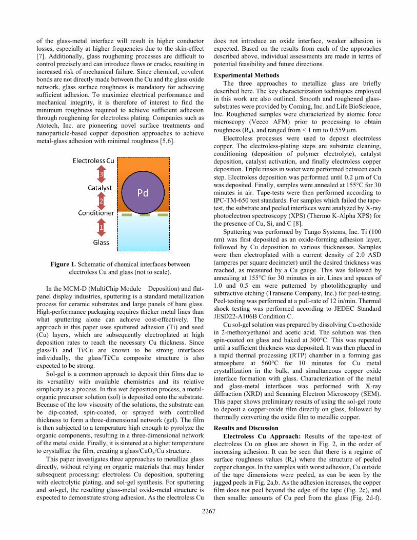
Electroless Cu Approach: Results of the tape-test of
electroless Cu on glass are shown in Fig. 2, in the order of
increasing adhesion. It can be seen that there is a regime of
surface roughness values (Ra) where the structure of peeled
copper changes. In the samples with worst adhesion, Cu outside
of the tape dimensions were peeled, as can be seen by the
jagged peels in Fig. 2a,b. As the adhesion increases, the copper
film does not peel beyond the edge of the tape (Fig. 2c), and
then smaller amounts of Cu peel from the glass (Fig. 2d-f).
2267
Finally, the glass chemically roughened to 0.559 μm passed the
tape test, exhibiting no peeled Cu (Fig. 2g).
(a) (b) (c)
(d) (e)
(f) (g)
Figure 2. Tape tests for electroless copper on various glasses:
(a) Corning SGW8.5 (Ra = 0.5 nm) (b) Corning SGW3 (Ra =
1.2 nm) (c) Corning SGW3 (Ra = 0.9 nm) (d) Corning
SGW8.5 (Ra = 1.3 nm) (e) Corning SGW8.5 (Ra = 19 nm) (f)
Corning SGW8.5 (Ra = 46 nm) (g) Life BioScience APEX (Ra
= 0.559 µm).
The large range in tape-test results for similar roughness
values (Fig. 2a-d) can be attributed to several factors.
Roughness values were measured with AFM and could vary
depending on the selected area because the topography was
generally not homogenous in the areas inspected (10x10 μm
and 30x30 μm). The values in this range are within the
instrumental error. In addition to surface roughness, adhesion
to glass depends on the glass chemical composition. High CTE
glasses (SGW8.5) are composed of more glass network-
modifying ions than low CTE glasses (SGW3); as these ions
are positively charged, they can assist with adhesion to the Pd
catalysts.
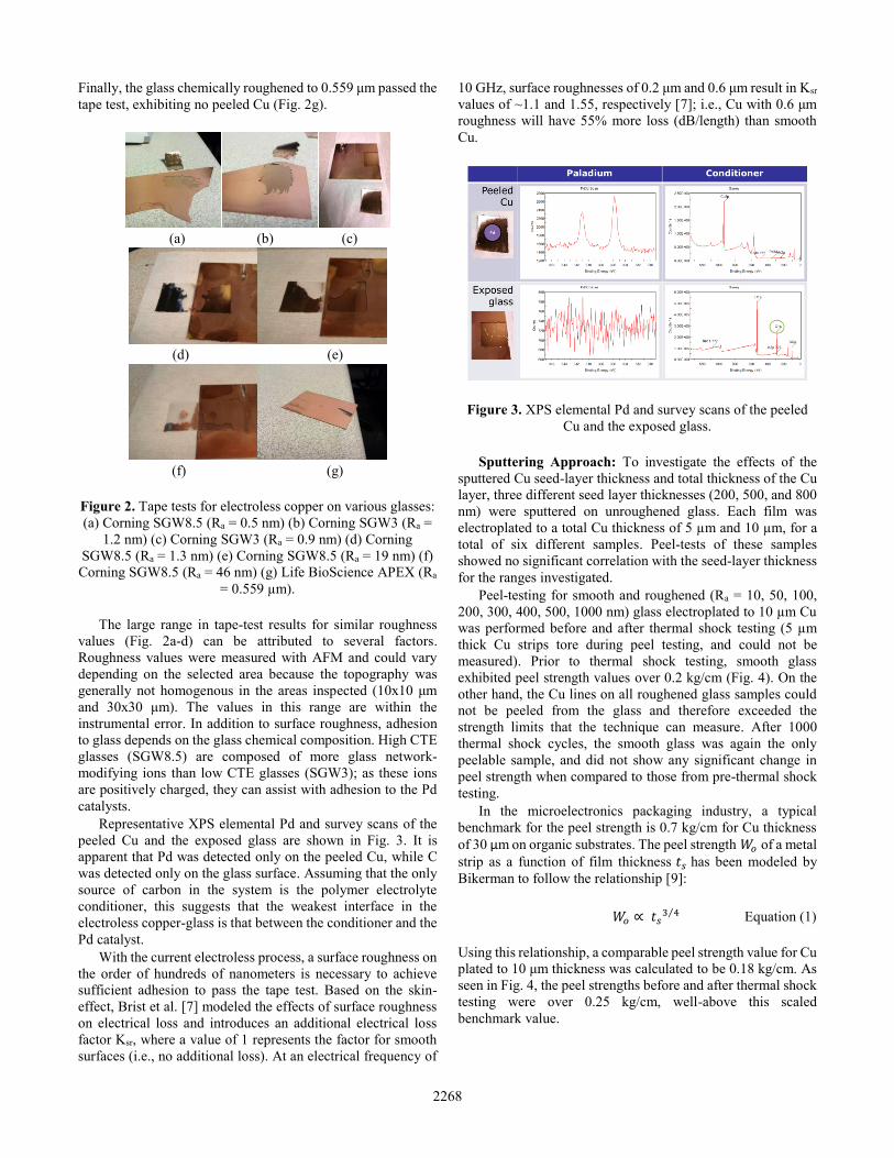
Representative XPS elemental Pd and survey scans of the
peeled Cu and the exposed glass are shown in Fig. 3. It is
apparent that Pd was detected only on the peeled Cu, while C
was detected only on the glass surface. Assuming that the only
source of carbon in the system is the polymer electrolyte
conditioner, this suggests that the weakest interface in the
electroless copper-glass is that between the conditioner and the
Pd catalyst.
With the current electroless process, a surface roughness on
the order of hundreds of nanometers is necessary to achieve
sufficient adhesion to pass the tape test. Based on the skin-
effect, Brist et al. [7] modeled the effects of surface roughness
on electrical loss and introduces an additional electrical loss
factor Ksr, where a value of 1 represents the factor for smooth
surfaces (i.e., no additional loss). At an electrical frequency of
10 GHz, surface roughnesses of 0.2 μm and 0.6 μm result in Ksr
values of ~1.1 and 1.55, respectively [7]; i.e., Cu with 0.6 μm
roughness will have 55% more loss (dB/length) than smooth
Cu.
Figure 3. XPS elemental Pd and survey scans of the peeled
Cu and the exposed glass.
Sputtering Approach: To investigate the effects of the
sputtered Cu seed-layer thickness and total thickness of the Cu
layer, three different seed layer thicknesses (200, 500, and 800
nm) were sputtered on unroughened glass. Each film was
electroplated to a total Cu thickness of 5 µm and 10 µm, for a
total of six different samples. Peel-tests of these samples
showed no significant correlation with the seed-layer thickness
for the ranges investigated.
Peel-testing for smooth and roughened (Ra = 10, 50, 100,
200, 300, 400, 500, 1000 nm) glass electroplated to 10 µm Cu
was performed before and after thermal shock testing (5 µm
thick Cu strips tore during peel testing, and could not be
measured). Prior to thermal shock testing, smooth glass
exhibited peel strength values over 0.2 kg/cm (Fig. 4). On the
other hand, the Cu lines on all roughened glass samples could
not be peeled from the glass and therefore exceeded the
strength limits that the technique can measure. After 1000
thermal shock cycles, the smooth glass was again the only
peelable sample, and did not show any significant change in
peel strength when compared to those from pre-thermal shock
testing.
In the microelectronics packaging industry, a typical
benchmark for the peel strength is 0.7 kg/cm for Cu thickness
of 30 µm on organic substrates. The peel strength 𝑊𝑜 of a metal
strip as a function of film thickness 𝑡𝑠 has been modeled by
Bikerman to follow the relationship [9]:
𝑊𝑜 ∝ 𝑡𝑠3 4⁄ Equation (1)
Using this relationship, a comparable peel strength value for Cu
plated to 10 μm thickness was calculated to be 0.18 kg/cm. As
seen in Fig. 4, the peel strengths before and after thermal shock
testing were over 0.25 kg/cm, well-above this scaled
benchmark value.
2268
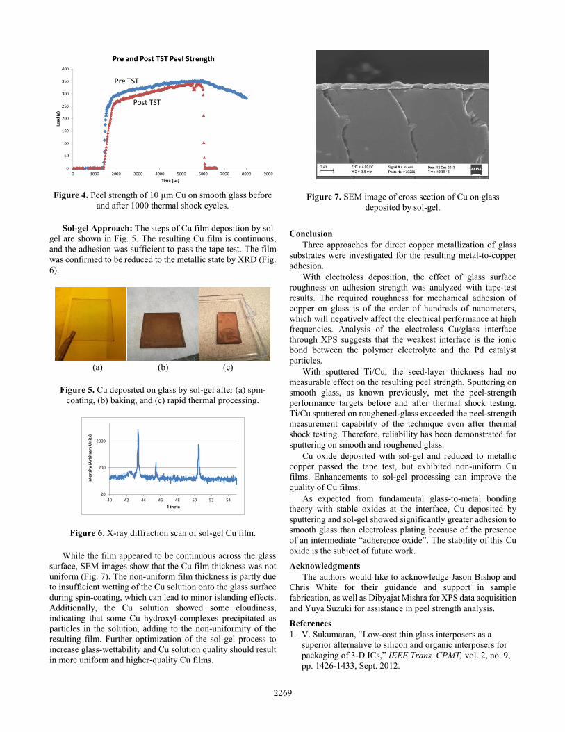
Figure 4. Peel strength of 10 µm Cu on smooth glass before
and after 1000 thermal shock cycles.
Sol-gel Approach: The steps of Cu film deposition by sol-
gel are shown in Fig. 5. The resulting Cu film is continuous,
and the adhesion was sufficient to pass the tape test. The film
was confirmed to be reduced to the metallic state by XRD (Fig.
6).
(a) (b) (c)
Figure 5. Cu deposited on glass by sol-gel after (a) spin-
coating, (b) baking, and (c) rapid thermal processing.
Figure 6. X-ray diffraction scan of sol-gel Cu film.
While the film appeared to be continuous across the glass
surface, SEM images show that the Cu film thickness was not
uniform (Fig. 7). The non-uniform film thickness is partly due
to insufficient wetting of the Cu solution onto the glass surface
during spin-coating, which can lead to minor islanding effects.
Additionally, the Cu solution showed some cloudiness,
indicating that some Cu hydroxyl-complexes precipitated as
particles in the solution, adding to the non-uniformity of the
resulting film. Further optimization of the sol-gel process to
increase glass-wettability and Cu solution quality should result
in more uniform and higher-quality Cu films.
Figure 7. SEM image of cross section of Cu on glass
deposited by sol-gel.
Conclusion
Three approaches for direct copper metallization of glass
substrates were investigated for the resulting metal-to-copper
adhesion.
With electroless deposition, the effect of glass surface
roughness on adhesion strength was analyzed with tape-test
results. The required roughness for mechanical adhesion of
copper on glass is of the order of hundreds of nanometers,
which will negatively affect the electrical performance at high
frequencies. Analysis of the electroless Cu/glass interface
through XPS suggests that the weakest interface is the ionic
bond between the polymer electrolyte and the Pd catalyst
particles.
With sputtered Ti/Cu, the seed-layer thickness had no
measurable effect on the resulting peel strength. Sputtering on
smooth glass, as known previously, met the peel-strength
performance targets before and after thermal shock testing.
Ti/Cu sputtered on roughened-glass exceeded the peel-strength
measurement capability of the technique even after thermal
shock testing. Therefore, reliability has been demonstrated for
sputtering on smooth and roughened glass.
Cu oxide deposited with sol-gel and reduced to metallic
copper passed the tape test, but exhibited non-uniform Cu
films. Enhancements to sol-gel processing can improve the
quality of Cu films.
As expected from fundamental glass-to-metal bonding
theory with stable oxides at the interface, Cu deposited by
sputtering and sol-gel showed significantly greater adhesion to
smooth glass than electroless plating because of the presence
of an intermediate “adherence oxide”. The stability of this Cu
oxide is the subject of future work.
Acknowledgments
The authors would like to acknowledge Jason Bishop and
Chris White for their guidance and support in sample
fabrication, as well as Dibyajat Mishra for XPS data acquisition
and Yuya Suzuki for assistance in peel strength analysis.
References
1. V. Sukumaran, “Low-cost thin glass interposers as a
superior alternative to silicon and organic interposers for
packaging of 3-D ICs,” IEEE Trans. CPMT, vol. 2, no. 9,
pp. 1426-1433, Sept. 2012.
20
200
2000
40 42 44 46 48 50 52 54
Inte
nsi
ty (
Arb
itra
ry U
nit
s)
2 theta
2269
2. V. Sukumaran, “Through-package-via formation and
metallization of glass interposers,” in Proc. IEEE
Electronic Components and Technol. Conf. (ECTC), Las
Vegas, NV, Jun. 1-4, 2010, pp. 557-563.
3. P. Benjamin, “The adhesion of evaporated metal films on
glass,” Proc. R. Soc. Lond. A, vol. 261, no. 1307, pp 516-
531, May 1961.
4. N. Jiang, “Observations of reaction zones at
chromium/oxide glass interfaces,” J. Appl. Phys., vol.87,
no. 8, pp. 3768-3776, Apr. 2000.
5. S. Bamberg, “Novel wet chemical metallization for glass
interposers”, 3D Materials and Processes Session,
International Conference on Device Packaging,
Scottsdale/Fountain Hills, AZ, Mar. 7-10, 2011.
6. R. Taylor, “Challenges of Adhesion Promotion for
Metallization of Glass Interposers”in Global Interposer
Technology Workshop (GIT), Atlanta, GA, Nov. 17-20,
2013.
7. G. Brist, “Non-classical conductor losses due to copper
foil roughness and treatment,” in Proc. Electron. Circuits
World Conv. (ECWC), Anaheim, CA, Feb. 22-24, 2005,
pp. 22-24.
8. X. Cui, “Copper deposition and patterning for glass
substrate manufacture,” in IEEE Trans. Electronics
Packaging Technol. Conf. (EPTC), Singapore, Dec. 10-12,
2007, pp. 37-42.
9. C. Jouwersma, “On the theory of peeling,” Journal of
Polymer Science, vol. 45, issue 145, pp. 253-255, July
1960.
2270