Embed Size (px)
Citation preview

IEEE TRANSACTIONS ON INDUSTRY APPLICATIONS, VOL. IA-12t NO. 3, MAY/JUNE 1976
Adjustable Voltage and Frequency Polyphase SineWave Signal Generator
JOHN P. WALDEN AND FRED G. TURNBULL, MEMBER, IEEE
Abstract-An adjustable-voltage adjustable-frequency polyphasereversible-phase sequence sine wave signal generator is described. Thissignal generator develops the reference waveforms, in this case sinewaves, that are required in the control circuits of certain types ofstatic dc to ac inverters and ac to ac cycloconverters. Digital and linearintegrated circuits together with passive components are used to gener-rate the output signals. The output frequency is adjustable from 0 to500 hertz; the output voltage is adjustable from 0 to 20 volts peak-to-peak. The phase sequence is reversible on command. The theoryof operation together with steady-state and transient performance dataare presented.
INTRODUCTION
A CONTROL circuit function required by static dc to acinverters and ac to ac cycloconverters is the generation of
an adjustable-voltage adjustable-frequency polyphase sine wavesignal. This signal is the reference waveform which is combinedwith other logic signals to control the operation of the powerswitches, such as thyristors or transistors, in the correct man-ner so as to provide a high quality sinusoidal output waveformto the load. Fig. 1 shows this circuit requirement as a part ofa complete motor control system. Three input signals are re-quired: 1) an analog dc voltage that controls the magnitudeof all of the sine wave output signals; 2) a digital pulse train(clock pulse) that controls the frequency of all of the sinewave output signals; and 3) a digital signal that controls thephase sequence of the sine wave output signals. All of theseinput signals operate independently and without interaction.The three output signals, developed by digital-to-analog(D/A) conversion techniques, are low distortion sinusoidalstepped waves which are digitally locked in a fixed 1200relationship. The three output signals are connected togetherat a common point and each can sustain a short circuit on itsoutput. In order to provide for maximum flexibility, noattempt has been made to establish a relationship or tie be-tween any of the input signals. For example, the voltage mag-nitude signal and the frequency determining pulses have Inotbeen tied together in order to provide an output signal with aconstant volts per hertz characteristic. Of course, this can beeasily accomplished and would result in a reference waveformsuitable for use in an adjuatable speed ac motor drive. Also, noattempt has been made to compare the output sine waves withany other analog waveforms as is sometimes required in static
Paper TOD-75-43, approved by the Static Power Converter Commit-tee of the IEEE Industry Applications Society for presentation at the1974 Ninth Annual Meeting of the IEEE Industry Applications Society,Pittsburgh, PA, October 7-10. Manuscript released for publication May5, 1975.
The authors are with the General Electric Company, Schenectady,NY 12301.
DC ACTI>Ow
DC PULSE WIDTH TACHOMETERSOURCE MODULATED.iMORJ v
SINE WAvE 3-TPHASEA-Ct rTTT OUTPUT
GATE DRIVERS ROTOR
AND COMPARATOR - SIGNALSPE
f __ t- SINE WAVE OUTPUTS
_SINE WAVE , MAG.A{TUDE SLP
GENERATOR COMMAND COMMANDGENERATOR ~ OLAG-T
FREQUENCY VORAEQUENCCOMMAND FRQEC
PHASE SEQUENCE COMMAND CONVERTER
Fig. 1. AC motor drive showing waveform generator subsystem.
pulsewidth modulated inverters. For example, an adjustablefrequency sine wave can be compared with a hiigh frequencytriangle wave in order to provide a pulsewidth modulated out-
put signal. This pulsewidth miodulated signal controls theoperation of the power switches [Ill, [31
SPECIFICATIONS
The electrical specifications for this reference waveformgenerator can be summarized as follows.
1) Range of output frequency-continually adjustable fromo (dc) to 500 hertz. If the clock pulses are stopped, the out-
put voltages maintain their correct values.2) Range of output voltage adjustment from 0 to 20 volts
peak-to-peak.3) Number of phases-three, easily extendable to six or
more.4) Output voltage waveshape-stepped wave sinusoidal,
with less than 1 percent total harmonic distortion over a "25to 1 range in output voltage.
5) Phase sequence of output voltages-reversible.6) Rate of change of output voltage-limited by the slew
rate of the f-inal operational amplifiers and the energy storedin the output filter.
THEORY OF OPERATION
GeneralA simplified block diagram of the system is shown in Fig.
2. The frequency command, which determines the outputfrequency, is a pulse train whiich is compatible withi digitalintegrated circuits. One hundred and ninety two clock pulsesare required at the input to produce a complete cycle of theoutput. Therefore, the output waveform can be controlled or
stepped to a precision of 360/19'2 or 1.875 degrees of thefundamental. These clock pulses are processed by digitalintegrated circuits to 1) develop the fundamental output
3 1 2
WALDEN AND TURNBULL: POLYPHASE SINE WAVE SIGNAL GENERATOR
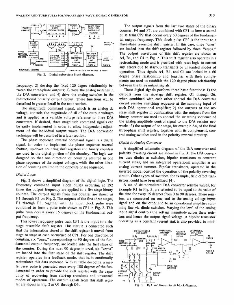
(FOR) FIVE STAGE FO)THREE STAGEfREQUENC S1NARY F5Ri C P2 SHIFT/L EFTCOMMAND FLIPDO WNUF/LT CONVRTER SHIFT/RIGH T
(REV)__ Fl F2 F3 F4 F5 Vi- REGISTER
r --- ~~~~~~~~~A4B4 C4
f r eq) d e lo p tFthFi xeF3dV Ft 03 F203 F3d r3 Pr tAoSp E A
I' t ~~~CPI'PHASE
t t3 d t a s ts
SEOUENCE PHASE1 -ICJRNSlK POLA RITYnREVERSuL SIX-STAGE s2 t iA REVERSINGCOMMAND FLIP/FLOP
(FOR) SHIFT/LEFT- 03 _,:0 CONVERTER _ SWITCH A-CREeFRADSHIFT/RIGHT 04 _C' OPAND OPAMP_ND
REVERSE 06 _2PHASE A PHASE A PHASE A
MAGNITUDE COMMAND _ _/SIMILAR CIRCUITS FOR PHASES B AND C
Fig. 2. Digital subsystem block diagram.
frequency; 2) develop the fixed 120 degree relationship be-tween the three-phase outputs; 3) drivhe analog switches inthe D/A converters; and 4) drive the analog switches in thebidirectional polarity output circuit. These functions will bedescribed in greater detail in the next section.
The magnitude command signal, which is an analog dcvoltage, controls the magnitude of all of the output voltagesand is applied as a variable voltage reference to three D/Aconverters. If desired, three magnitude command signals canbe easily implemented in order to allow independent adjust-ment of the individual output waves. The D/A conversiontechnique will be described in a later section.
The phase sequence reversal command signal is a digitalsignal. In order to implement the phase sequence reversalfeature, up-down counting shift registers and binary countersare used in the digital portion of the circuitry. The logic wasdesigned so that one direction of counting resulted in onephase sequence of the output voltages, while the other direc-tion of counting resulted in the opposite phase sequence.
Digital Logic
Fig. 2 shows a simplified diagram of the digital logic. The
frequency command input clock pulses occurring at 192times the output frequency are applied to a five-stage binarycounter. The output signals from this counter are shown asFl through F5 on Fig. 2. The outputs of the first three stages,Fl through F3, together with the input clock pulse were
combined to form a pulse train shown as CPI in Fig. 2. This
pulse train occurs every 15 degrees of the fundamental out-
put frequency.This lower frequency pulse train CPI is the input to a six-
stage reversible shift register. This circuit is connected suchthat the information stored in the shift register is moved fromstage to stage at each occurence of CPI. For one direction ofcounting, six "ones," corresponding to 90 degrees of the fun-damental output frequency, are loaded into the first stage ofthe counter. During the next 90 degree interval, six "zeros"are loaded into the first stage of the shift register. The shiftregister operates in a feedback mode, that is, it continuallyrecirculates this data sequence. With suitable decoding, a mas-ter reset pulse is generated once every 180 degrees of the fun-damental in order to provide the shift register with the capa-bility of recovering from start-up transients and unwantedmodes of operation. The output signals from this shift regis-ter are shown in Fig. 2 as QI through Q6.
The output signals from the last two stages of the binarycounter, F4 and F5, are combined with CPl to form a secondpulse train CP2 that occurs every 60 degrees of the fundamen-tal output frequency. This clock pulse CP2 is the input to athree-stage reversible shift register. In this case, three "ones"are loaded into the shift register followed by three "zeros."The output waveforms of this shift register are shown asA4, B4, and C4 in Fig. 2. This shift register also operates in arecirculating mode and is provided with reset logic to correctany errors due to start-up transients or unwanted modes ofoperation. Thus signals A4, B4, and C4 are locked in a 60degree phase relationship and together with their comple-ments are used to establish the 120 degree phase relationshipbetween the three output signals.
These digital signals perform three basic functions: 1) theoutputs from the six-stage shift register, Ql through Q6,when combined with each other control the D/A convertercircuit resistor switching sequence at the summing input ofeach D/A operational amplifier; 2) the outputs of the six-stage shift register in combination with the outputs from thebinary counter are used to control the switching sequence ofthe analog amplitude control signal to the D/A resistor net-works; 3) the output of one stage, for example A4, of the finalthree-phase shift register, together with its complement, con-trol analog switches used in the polarity reversal circuitry.
Digital to Analog Converter
A simplified schematic diagram of the D/A converter andpolarity reversing circuit are shown in Fig. 3. The D/A conver-ter uses diodes as switches, bipolar transistors as constantcurrent sinks, and an integrated operational amplifier as ananalog current summer. Bipolar transistors, operated in theinverted mode, control the operation of the polarity reversingcircuit. Other types of switches, for example, field effect tran-sistors, could have been utilized [4].A set of six normalized D/A converter resistor values, for
example RI in Fig. 3, are selected to be equal to the value ofthe sine for every 15 degrees from 0 to 90 degrees. These resis-tors are connected on one end to the analog voltage inputsignal and on the other end to an operational amplifier sum-ming line via diode switches. Varying the level of the analoginput signal controls the voltage magnitude across these resis-tors and hence the output signal voltage. A bipolar transistoroperating as a constant current sink is also provided to mini-
Fig. 3. D/A and linear circuit block diagram.
313

IEEE TRANSACTIONS ON INDUSTRY APPLICATIONS, MAY/JUNE 1976
mize the loading on the analog input control line as it isvaried over the full control range. The diode switches arecontrolled by the decoded outputs of the six-stage shiftregister, for example, signals Q I and Q5.
In order to develop a smoother sine wave signal, a linearinterpolation is provided between each 15 degree segment.This linear interpolation has eight steps between 0 and 150,150 and 300, 300 and 450, and 450 and 60°. Between 600and 750, four linear steps are provided. Between 750 and 900,two linear steps are provided. The slope of a sine wave is lessbetween 600 and 900, therefore, less steps are needed to forman accurate sine wave output. These linear interpolations areaccomplished by an additional resistor network connected tothe D/A summing line. These resistors, for example, R2 shownin Fig. 3, are switched at the D/A summing line in response todecoded output signals from the six-stage shift register, Qlthrough Q6. Three resistors and diode switches are shown inFig. 3, resulting in an eight step linear interpolation of a given15 degree interval. During the 15 degree intervals when foursteps are provided, only two resistors and diode switches areprovided. The opposite end of these resistors is connected tothe analog output level signal via a second switching network.This second switching network is controlled primarily by thebinary counter signals Fl, F2, and F3. The basic operatingconcepts of this arrangement are 1) to obtain the relativemagnitude and the number of steps per 15 degree segment byparalleling more or less resistors by means of the summingline switching network and 2) to combine the resistors in abinary adding sequence to generate the stepped ramps and tocontrol the overall magnitude of the ramps by means of theanalog output level switching network. The complements ofthe signals Fl, F2, and F3 are combined in a "wired-OR"configuration with the appropriate Ql through Q6 signals inorder to provide linear negative steps during the interval from90 degrees to 180 degrees.
The use of the same D/A circuit components (resistors,switches, and current sinks) for the interval from 90 to 180degrees as was used to generate the waveform from 0 to 90degrees, resulted in a symmetrical waveform with respect tothe 90 degree point. This was a desirable objective since itwould tend to eliminate even order harmonics in the outputvoltage. The output from the operational amplifier could bestbe described as an adjustable-amplitude full-wave rectifiedsinusoid at the fundamental output frequency.
Polarity Reversing Circuit
The output from the D/A operational amplifier is the inputto the polarity reversing circuitry shown in Fig. 3. The outputof the three-stage shift register, for example, A4 and its com-plement, alternately energizes transistors TI and T2 at thefundamental frequency. With the arrangement shown, the out-put operational amplifier is, therefore, switched from aninverting configuration to a noninverting one. Proper selectionof the resistor values allows the gain and offset to be the samefor either half cycle of the output. With this arrangement,alternate 180 degree segments of the D/A output signal areinverted to produce a normal ac sine wave with respect to
In order to remove some of the switching transients asso-ciated with the D/A network, an RC filter was provided atthe output of the waveform generator. The break frequency ofthe filter was selected to be greater than ten times the maxi-mum expected output frequency (500 hertz). Precision resis-tors and capacitors were utilized so that the fundamentalfrequency phase shift associated withl each of the outputphases could be within well defined limits.
Phase Sequence Reversal
The phase sequence of the output voltages is determined bya digital input signal that could occur at any point in time. Thenormal counting, gating, and shifting of information in thedigital circuits occurs at the falling edge of the frequencydetermining input clock pulse. A change in the phase sequencecommand signal during this interval of time is to be avoidedsince logic upsets may occur. In order to eliminate this possi-bility, a one-shot multivibrator with a one-microseconid pulse-width is triggered at the end of each frequency clock pulse andis used to clock the phase reversal flip-flop. The falling edge ofthis delayed pulse controls the time at which the flip-flop can
change state. The logic input signal to this flip-flop is the phasesequence input command. This arrangement is shown in Fig. 2.The operation of the delayed clock pulse and flip-flop madethe phase sequence command effective one microsecond afterthe next clock pulse and thus cannot interfere with the fre-quency clock pulse. A change in the phase sequence of theoutput fundamentally requires a change in the direction ofcounting for the five-stage up/down binary counter, signalsFl through F5 and shift right/shift left capability for the six-stage shift register, signals Ql through Q6 and the three-stageshift register signals A4, B4, and C4. The direction mode forthe counter and registers plus the logical position of the sys-tem's various synchronizing pulses is determined by the stateof the phase reversal flip-flop.
PERFORMANCE DATA
A complete three-phase signal generator is mounted on thefour printed circuit boards shown in Fig. 4. The digital portionof the circuit is contained on one board. The D/A converterand ac output operational amplifier associated with each phaseis mounted on a separate printed circuit board.
Output Voltage ControlThe RMS ac output voltage versus the dc input voltage
transfer characteristic is shown in Fig. 5. This characteristiccould be modified and the gain changed by the addition of an
operational amplifier at the input. Operation with dc inputvoltages in excess of plus five volts does not damage the inputcircuitry but only further reverse biases several input diodes.
The output voltage waveform for one phase for severalvalues of magnitude command signal is shown superimposedin Fig. 6. The photograph shows that control of the outputvoltage magnitude does not introduce any phase shift in theoutput voltage. The total harmonic content of the outputvoltage waveform at 4Q0 hertz and the maximum output was
circuit ground.
3 14
measured at 0.54 percent. The total harmonic content at 40
WALDEN AND TURNBULL: POLYPHASE SINE WAVE SIGNAL GENERATOR 315
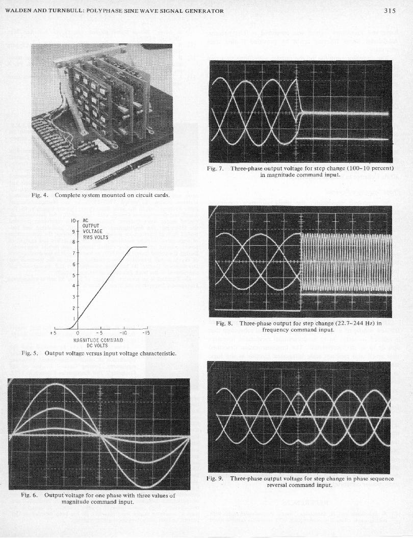
Fig. 7. Three-phase output voltage for step change (100- 10 percent)in magnitude command input.
Fig. 4. Complete system mounted on circuit cards,
71
6
5
4
3.'
2
ACOUTPUTVOLTAGERMS VOLTS
+5 0 -5 -10 -15MAGNITUDE COMMAND
DC VOLTSFig. 5. Output voltage versus input voltage characteristic.
Fig. 8. Three-phase output for step change (22.7-244 Hz) infrequency command input.
Fig. 9. Three-phase output voltage for step change in phase sequencereversal command input.
Fig. 6. Output voltage for one phase with three values ofmagnitude command input.

IEEE TRANSACTIONS ON INDUSTRY APPLICATIONS, MAY/JUNE 1976
hertz and maximum output was measured at 0.81 percent.Additional linear filtering could be provided if this werenecessary.
The transient response of the output waveforms to a stepchange in magnitude command signal is shown in Fig. 7 for adecrease in magnitude corresponding to 100 percent to 10percent of full output. The response time in both increasingand decreasing signals is approximately 100 microseconds.
Output Frequency Control
The output frequency is directly related to the input clockrepetition rate. Since there is no energy storage or linear cir-cuits, the response of the system is instantaneous. The three-phase output signals for a step change in clock rate corre-sponding to 22.7 hertz to 244 hertz is shown in Fig. 8. Theoutput voltage magnitude does not change, and there are notransients generated in the system due to this greater than10 to 1 change in output frequency.
Phase Sequence Reversal
As described previously, the phase sequence commandtakes effect one microsecond after the end of the clock pulseoccurring after the change in phase sequence commandsignal. The three-phase output signals are shown in Fig. 9 for40 hertz. The smooth transient-free phase sequence reversal isclearly shown. The change in phase sequence is effective at anypoint in the output waveform; it does not wait for a certainangular position of the output signals. This feature allows forthe rapid reversal of the reference waveform phase sequencethat would normally be required at very low fundamentalfrequency outputs.
ac drives," Brown Boveri Review, vol. 51, no. 8-9, Aug./Sept.1964, pp. 555-577.
[2] B. D. Bedford and R. G. Hoft, Principles of Inverter Circuits.New York, Wiley, 1964, p. 261.
[3] B. Morkrytzki, "Pulse width modulated inverters for ac motordrives," 1966 IEEE International Convention Record, Pt. 8,pp. 8-23.
t4] J. J. Kubinec, "MOS analog function generator," National Semi-conductor Corp., 1968.
Fred G. Tumbull (M'60) received the B.S.E.E.and M.S.E.E. degrees from the University of
E El a California, Berkeley, in 1953 and 1959, respec-k ~~~~~~tively.
He is currently an Electronics Engineer withthe Electronic Power Conditioning and ControlLaboratory, Research and Development Center,General Electric Company, Schenectady, N.Y.He is at present engaged in power conversionstudies related to advanced drive systems andthe application of power semiconductors, cir-
cuits, and controls, to industrial, transportation, utility, and militarysystems. During the period 1969-1974, he was Manager-AdvancedDrive Systems Unit in the Solid State Power Control Branch at the Re-search and Development Center, with responsibility for developing ad-vanced motor drive systems. Projects under his supervision includedthe following: the development of pulsewidth modulated and con-trolled current inverters for motor drive applications; the constructionof high speed rotating machinery; and the simulation and analysis ofpower control systems using digital, analog, and hybrid computers.During the period from 1959-1969, he was engaged in the developmentof thyristor and transistor power control circuits at the Research andDevelopment Center. He has been awarded five U.S. patents and hascontributed to the book Principles ofInverter Circuits.
Mr. Turnbull is an associate member of Sigma Xi and is aRegisteredProfessional Engineer in the State of New York.
CONCLUSIONS
This paper has described the implementation and presentedthe test results of a flexible functional control subsystem thatis needed in static dc to ac pulsewidth modulated invertersand ac to ac cycloconverters. The implementation describeduses small and medium scale integrated circuits in the logiccircuits and linear integrated circuits and discrete componentsin the D/A converters. The availability of large scale integratedcircuits, MOS switches, and complete D/A converter moduleswould allow the equivalent function to be performed at lessvolume, with less interconnections, and possibly extendedfrequency range.
The system is expandable and flexible, and it can be easilyinterfaced with both input and output circuitry that arerequired by the static power system performance specifica-tions. The system provides a low-distortion low-impedancepolyphase, adjustable-voltage adjustable-frequency sine waveoutput signal. The time constants and phase shifts associatedwith this functional control subsystem are not significant anddo not become the limiting items in the design of a completestatic power converter system.
REFERENCES[1] A. Schonung and H. Stemamler, "Static frequency changers with
subharmonic control in conjunction with reversible variable speed
John P. Walden received the B.S.E.E. degreefrom Louisiana State University, Baton Rouge,in 1950.From 1950 to 1952 he worked with the
Civil Aeronautics Administration on the finalinstallation of communications and navigationequipment. Joining General Electric on theCompany's Test Engineering Program in 1952,he transferred a year later to the EngineeringStaff of General Electric's General EngineeringLaboratory. His early work pertained to the
application and development of circuits for eddy-current nondestruc-tive testing equipment, and the design of electronically regulated powersupplies, temperature measuring instrumentation for large generators,and analog data processing circuits. Following these activities, hisfield endeavor focused on the design and application of unique elec-tronic power systems. His activities have ranged from system engineer-ing responsibilities for a satellite power system to conducting investi-gations into the electrical aspects of electrohydraulic processing. Hisprincipal design responsibilities centered on signal level control circuitryand encompassed 6000C vacuum tube circuitry to compact transistor-ized circuitry for space applications. Presently he is employed as anElectronics Engineer with General Electric's Corporate Research andDevelopment. His recent work has been directed towards high fre-quency power conditioning equipment. He has acted as Project Engi-neer for both high power thyristor and low power transistor powerconversion circuits. His recent work has ranged from the developmentof specialized computer design programs, pulsewidth modulated con-trol circuitry, high power resonate inverter controls, to complete de-signs of transistor square wave inverters. He has been awarded six U.S.patents and has five patent applications pending.
316