Embed Size (px)
Citation preview
B. E. Boser 1
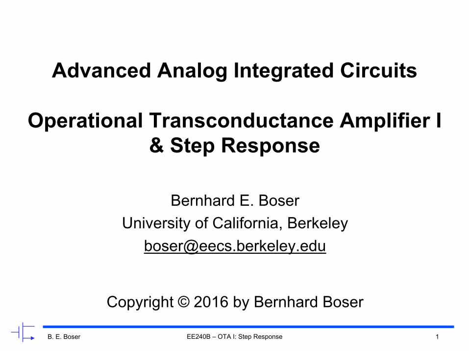
Advanced Analog Integrated Circuits
Operational Transconductance Amplifier I& Step Response
Bernhard E. BoserUniversity of California, Berkeley
Copyright © 2016 by Bernhard Boser
EE240B – OTA I: Step Response
B. E. Boser 2
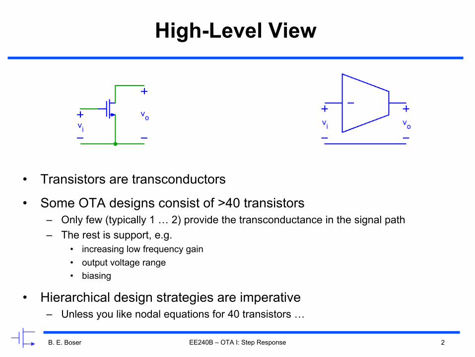
High-Level View
• Transistors are transconductors
• Some OTA designs consist of >40 transistors– Only few (typically 1 … 2) provide the transconductance in the signal path– The rest is support, e.g.
• increasing low frequency gain• output voltage range • biasing
• Hierarchical design strategies are imperative– Unless you like nodal equations for 40 transistors …
EE240B – OTA I: Step Response
B. E. Boser 3
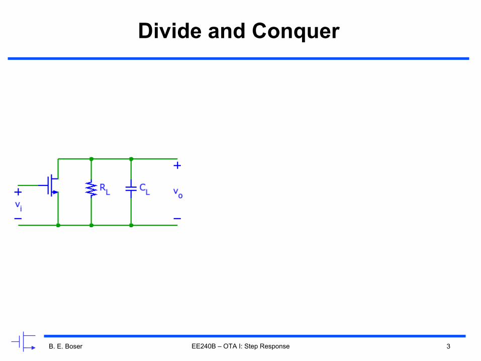
Divide and Conquer
EE240B – OTA I: Step Response

B. E. Boser 4
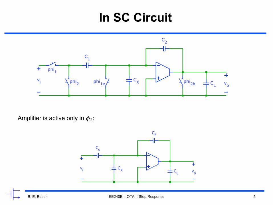
In SC Circuit
EE240B – OTA I: Step Response
B. E. Boser 5
In SC Circuit
EE240B – OTA I: Step Response
Amplifier is active only in 𝜙":
B. E. Boser 6
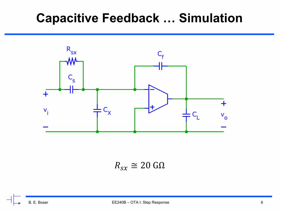
Capacitive Feedback … Simulation
𝑅$% ≅ 20GΩ
EE240B – OTA I: Step Response
B. E. Boser 7
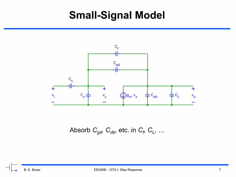
Small-Signal Model
Absorb Cgd, Cdb, etc. in Cf, CL, …
EE240B – OTA I: Step Response
B. E. Boser 8
Advanced Analog Integrated Circuits
Loop-Gain & Stability
Bernhard E. BoserUniversity of California, Berkeley
Copyright © 2016 by Bernhard Boser
EE240B – OTA I: Step Response
B. E. Boser 9
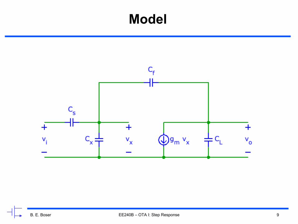
Model
EE240B – OTA I: Step Response
B. E. Boser 10
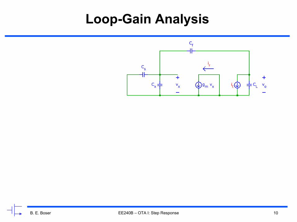
Loop-Gain Analysis
EE240B – OTA I: Step Response
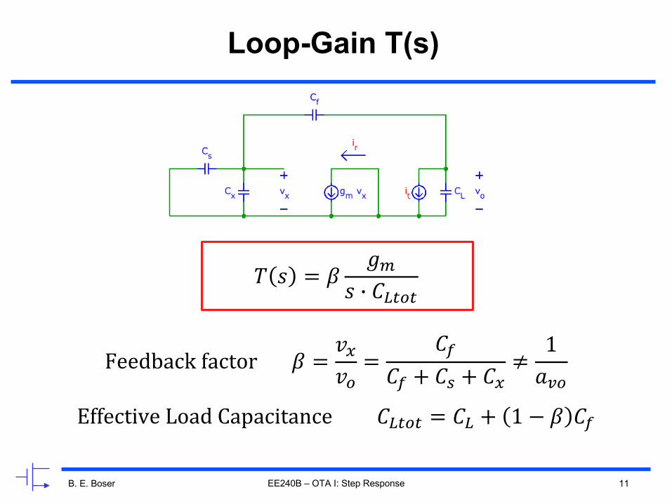
B. E. Boser 11
Loop-Gain T(s)
𝑇 𝑠 = 𝛽𝑔1
𝑠 2 𝐶4565
Feedbackfactor𝛽 =𝑣%𝑣6=
𝐶C𝐶C + 𝐶$ + 𝐶%
≠1𝑎H6
EffectiveLoadCapacitance𝐶4565 = 𝐶4 + 1 − 𝛽 𝐶C
EE240B – OTA I: Step Response
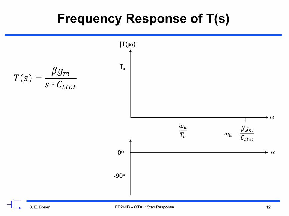
B. E. Boser 12
Frequency Response of T(s)
𝑇 𝑠 =𝛽𝑔1
𝑠 2 𝐶4565
EE240B – OTA I: Step Response
w
|T(jw)|
To
𝜔R =𝛽𝑔1𝐶4565
𝜔R𝑇6
-90o
0o w
B. E. Boser 13
Advanced Analog Integrated Circuits
Closed-Loop Response
Bernhard E. BoserUniversity of California, Berkeley
Copyright © 2016 by Bernhard Boser
EE240B – OTA I: Step Response
B. E. Boser 14
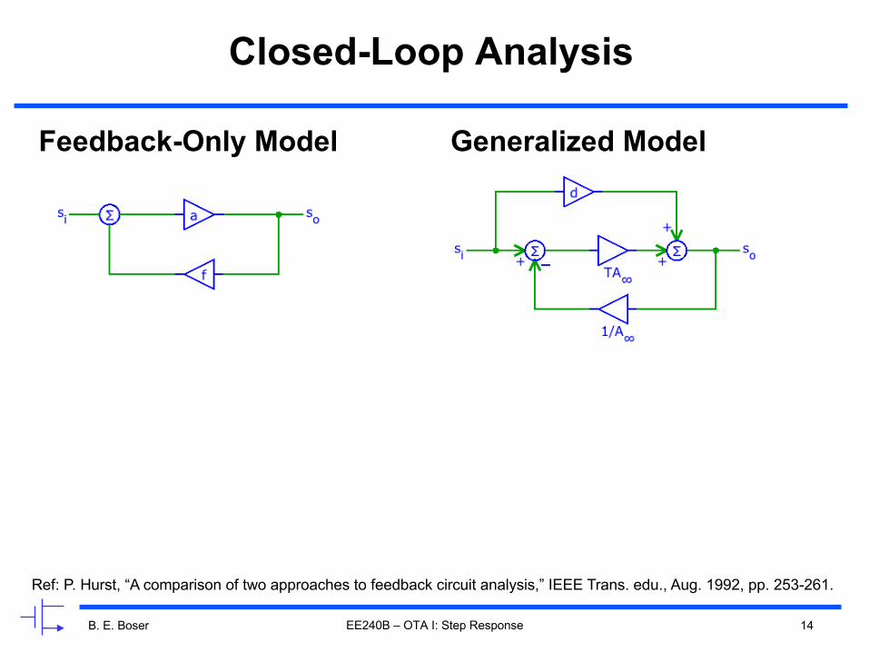
Closed-Loop Analysis
Feedback-Only Model Generalized Model
EE240B – OTA I: Step Response
Ref: P. Hurst, “A comparison of two approaches to feedback circuit analysis,” IEEE Trans. edu., Aug. 1992, pp. 253-261.

B. E. Boser 15
Closed-Loop Transfer Function
EE240B – OTA I: Step Response
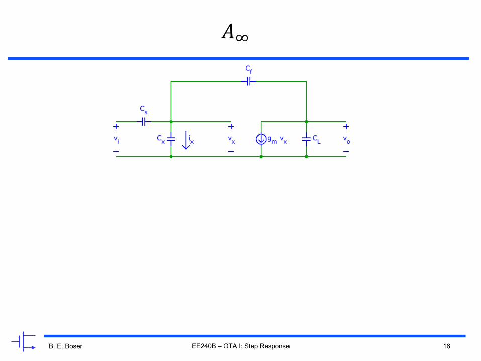
B. E. Boser 16
𝐴T
EE240B – OTA I: Step Response

B. E. Boser 17
𝑑
EE240B – OTA I: Step Response
B. E. Boser 18
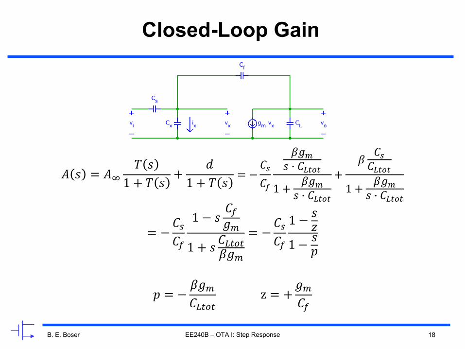
Closed-Loop Gain
𝐴 𝑠 = 𝐴T𝑇 𝑠
1 + 𝑇 𝑠 +𝑑
1 + 𝑇 𝑠 = −𝐶$𝐶C
𝛽𝑔1𝑠 2 𝐶4565
1 + 𝛽𝑔1𝑠 2 𝐶4565
+𝛽 𝐶$𝐶4565
1 + 𝛽𝑔1𝑠 2 𝐶4565
= −𝐶$𝐶C
1 − 𝑠𝐶C𝑔1
1 + 𝑠 𝐶4565𝛽𝑔1
= −𝐶$𝐶C
1 − 𝑠𝑧1 − 𝑠
𝑝
𝑝 = −𝛽𝑔1𝐶4565
z = +𝑔1𝐶C
EE240B – OTA I: Step Response
B. E. Boser 19
Advanced Analog Integrated Circuits
Stability and T(s) with Simulator
Bernhard E. BoserUniversity of California, Berkeley
Copyright © 2016 by Bernhard Boser
EE240B – OTA I: Step Response
B. E. Boser 20
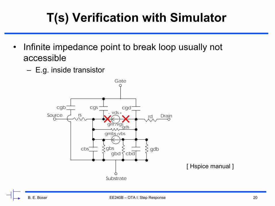
T(s) Verification with Simulator
• Infinite impedance point to break loop usually not accessible– E.g. inside transistor
EE240B – OTA I: Step Response
[ Hspice manual ]
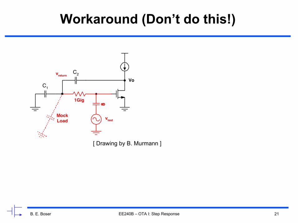
B. E. Boser 21
Workaround (Don’t do this!)
EE240B – OTA I: Step Response
Vo
1Gig¥
vreturn
vtestMockLoad
C1
C2
[ Drawing by B. Murmann ]
B. E. Boser 22
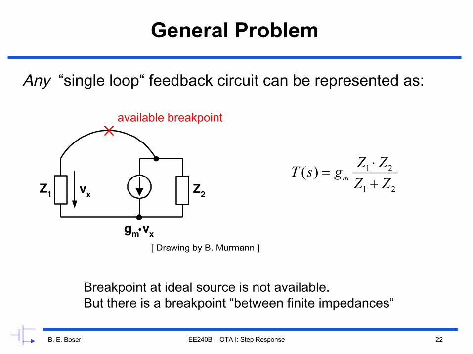
General Problem
Any “single loop“ feedback circuit can be represented as:
EE240B – OTA I: Step Response
gm×vx
vxZ1 Z2
Breakpoint at ideal source is not available.But there is a breakpoint “between finite impedances“
available breakpoint
21
21)(ZZZZgsT m +×
=
[ Drawing by B. Murmann ]
B. E. Boser 23
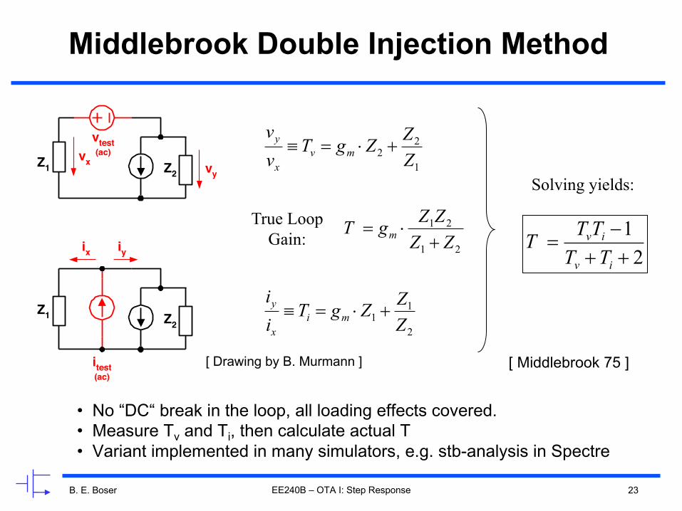
Middlebrook Double Injection Method
EE240B – OTA I: Step Response
Z1 Z2
iy
vxZ1 Z2 vy
vtest(ac)
itest(ac)
ix
1
22 ZZZgT
vv
mvx
y +×=º
2
11 ZZZgT
ii
mix
y +×=º
21
21
ZZZZgT m +
×=True Loop Gain:
Solving yields:
21++-
=iv
iv
TTTTT
• No “DC“ break in the loop, all loading effects covered.• Measure Tv and Ti, then calculate actual T• Variant implemented in many simulators, e.g. stb-analysis in Spectre
[ Middlebrook 75 ][ Drawing by B. Murmann ]
B. E. Boser 24
SPICE
EE240B – OTA I: Step Response

B. E. Boser 25
Multiple Feedback Loops
• Break all loops at a single point
• If such a point does not exist: [Bode 45]
“If a circuit is stable when all its tubes have their nominal gains, thetotal number of clockwise and counterclockwise encirclements of thecritical point must be equal to each other in the series of Nyquist diagrams for the individual tubes obtained by beginning with all tubesdead and restoring the tubes successively in any order to theirnominal gains”
– Suggestion: take a controls class if your circuit depends on this!
EE240B – OTA I: Step Response
B. E. Boser 26
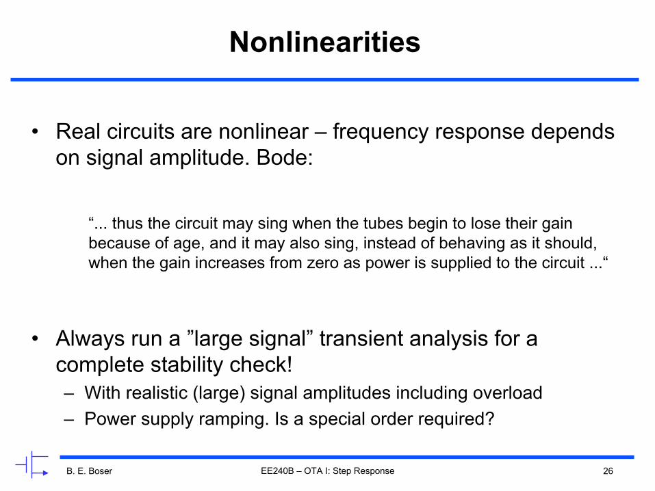
Nonlinearities
• Real circuits are nonlinear – frequency response depends on signal amplitude. Bode:
“... thus the circuit may sing when the tubes begin to lose their gainbecause of age, and it may also sing, instead of behaving as it should, when the gain increases from zero as power is supplied to the circuit ...“
• Always run a ”large signal” transient analysis for a complete stability check!– With realistic (large) signal amplitudes including overload– Power supply ramping. Is a special order required?
EE240B – OTA I: Step Response
B. E. Boser 27
Advanced Analog Integrated Circuits
Settling
Bernhard E. BoserUniversity of California, Berkeley
Copyright © 2016 by Bernhard Boser
EE240B – OTA I: Step Response
B. E. Boser 28
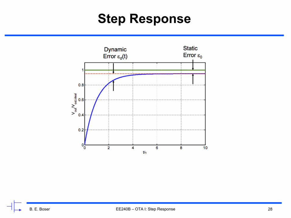
Step Response
EE240B – OTA I: Step Response
B. E. Boser 29
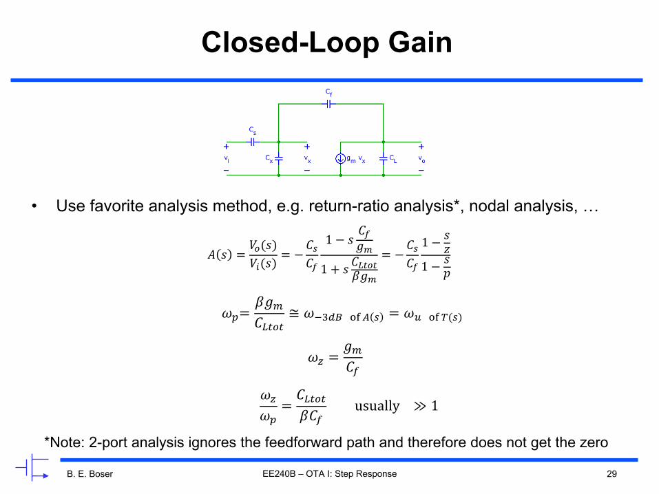
Closed-Loop Gain
• Use favorite analysis method, e.g. return-ratio analysis*, nodal analysis, …
EE240B – OTA I: Step Response
𝐴 𝑠 =𝑉6(𝑠)𝑉\(𝑠)
= −𝐶$𝐶C
1 − 𝑠𝐶C𝑔1
1 + 𝑠 𝐶4565𝛽𝑔1
= −𝐶$𝐶C
1 − 𝑠𝑧1 − 𝑠
𝑝
𝜔] =𝑔1𝐶C
*Note: 2-port analysis ignores the feedforward path and therefore does not get the zero
𝜔]𝜔^
=𝐶4565𝛽𝐶C
usually ≫ 1
𝜔^=𝛽𝑔1𝐶4565
≅ 𝜔defghij $ = 𝜔Rhik($)
B. E. Boser 30
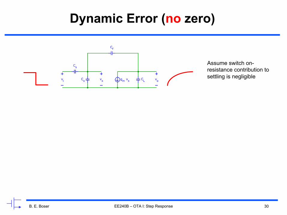
Dynamic Error (no zero)
EE240B – OTA I: Step Response
Assume switch on-resistance contribution to settling is negligible
B. E. Boser 31
Dynamic Settling Error
EE240B – OTA I: Step Response
B. E. Boser 32
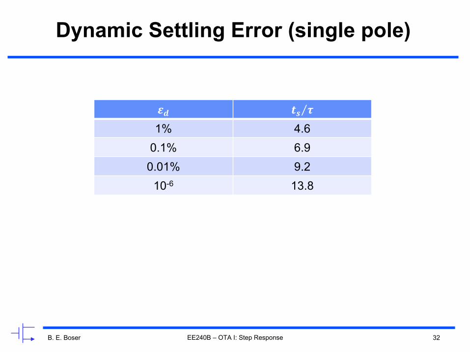
Dynamic Settling Error (single pole)
𝜺𝒅 𝒕𝒔 𝝉⁄1% 4.6
0.1% 6.90.01% 9.2
10-6 13.8
EE240B – OTA I: Step Response
B. E. Boser 33
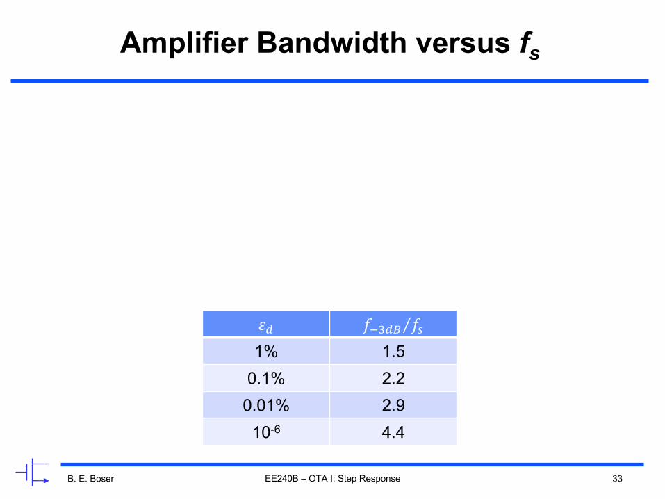
Amplifier Bandwidth versus fs
EE240B – OTA I: Step Response
𝜀f 𝑓defg 𝑓$⁄1% 1.5
0.1% 2.20.01% 2.9
10-6 4.4
B. E. Boser 34
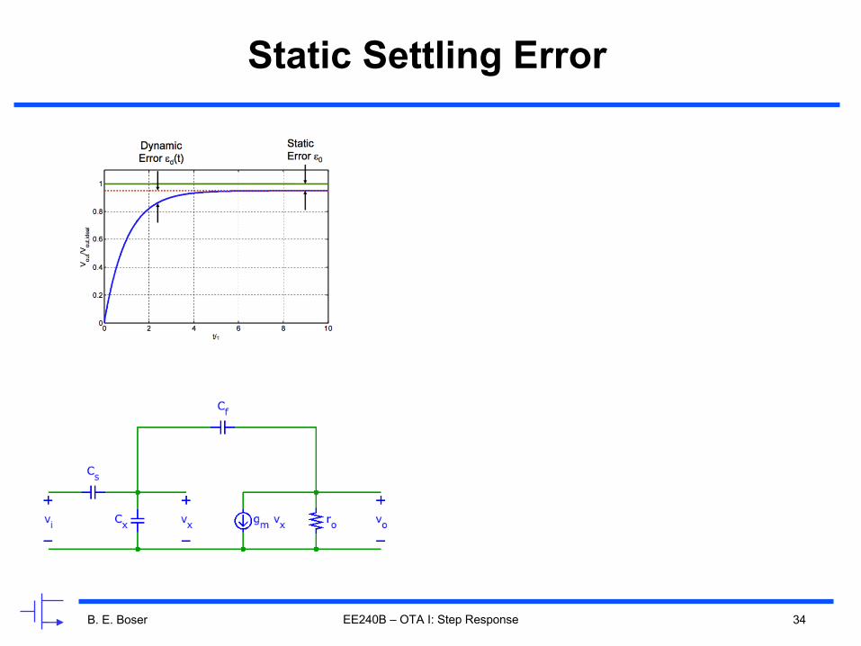
Static Settling Error
EE240B – OTA I: Step Response
B. E. Boser 35
Example
𝐶$ = 4pF𝐶C = 1pF𝐶% = 1pF𝑔1𝑟6 = 6000
EE240B – OTA I: Step Response

B. E. Boser 36
Dynamic Error (with zero)
• Instant response to step determined by capacitive feed-forward
𝐴 𝑠 =𝑉6(𝑠)𝑉\(𝑠)
= −𝐶$𝐶C
1 − 𝑠𝐶C𝑔1
1 + 𝑠 𝐶4565𝛽𝑔1
𝑧 = +𝑔1𝐶C𝑝 = −
𝛽𝑔1𝐶4565
EE240B – OTA I: Step Response
B. E. Boser 37
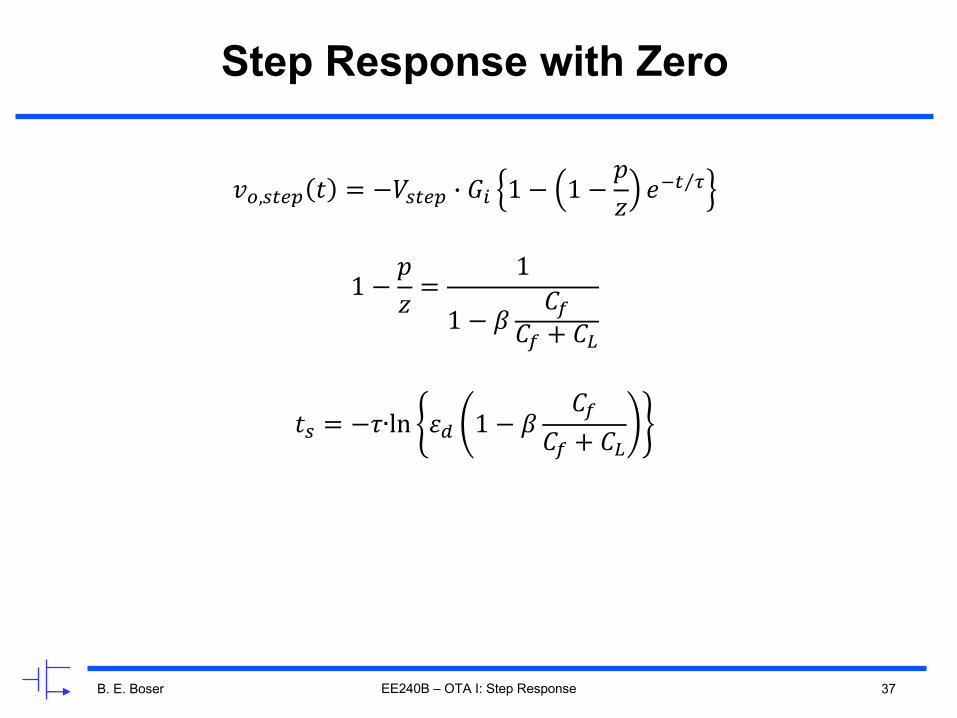
Step Response with Zero
𝑣6,$5x^ 𝑡 = −𝑉$5x^ 2 𝐺\ 1 − 1 −𝑝𝑧 𝑒d5 |⁄
1 −𝑝𝑧 =
1
1 − 𝛽𝐶C
𝐶C + 𝐶4
𝑡$ = −𝜏∙ln 𝜀f 1 − 𝛽𝐶C
𝐶C + 𝐶4
EE240B – OTA I: Step Response

B. E. Boser 38
Advanced Analog Integrated Circuits
Phase Margin
Bernhard E. BoserUniversity of California, Berkeley
Copyright © 2016 by Bernhard Boser
EE240B – OTA I: Step Response
B. E. Boser 39
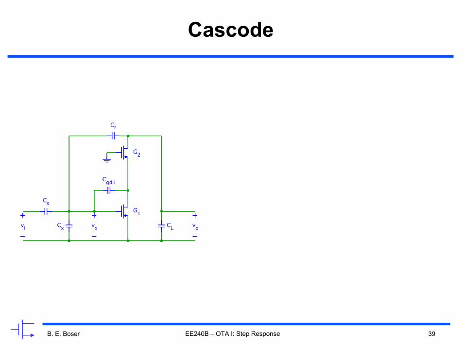
Cascode
EE240B – OTA I: Step Response
B. E. Boser 40
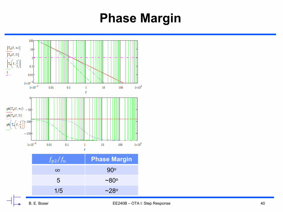
Phase Margin
EE240B – OTA I: Step Response
𝑓 " 𝑓R⁄ Phase Margin∞ 90o
5 ~80o
1/5 ~28o
B. E. Boser 41
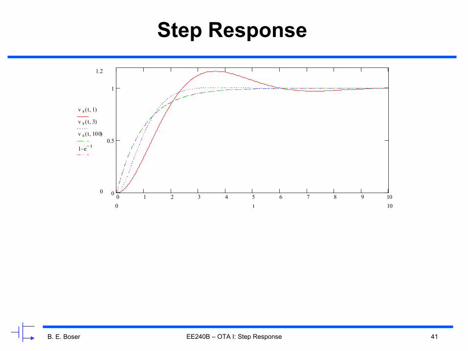
Step Response
EE240B – OTA I: Step Response
0 1 2 3 4 5 6 7 8 9 100
0.5
1
1.2
0
v s t 1,( )
v s t 3,( )
v s t 100,( )
1 e t--
100 t
B. E. Boser 42
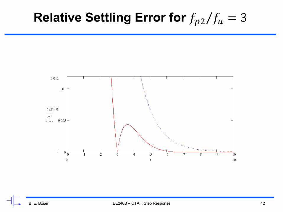
Relative Settling Error for 𝑓 " 𝑓R⁄ = 3
EE240B – OTA I: Step Response
0 1 2 3 4 5 6 7 8 9 100
0.005
0.01
0.012
0
e s t 3,( )
e t-
100 t
B. E. Boser 43
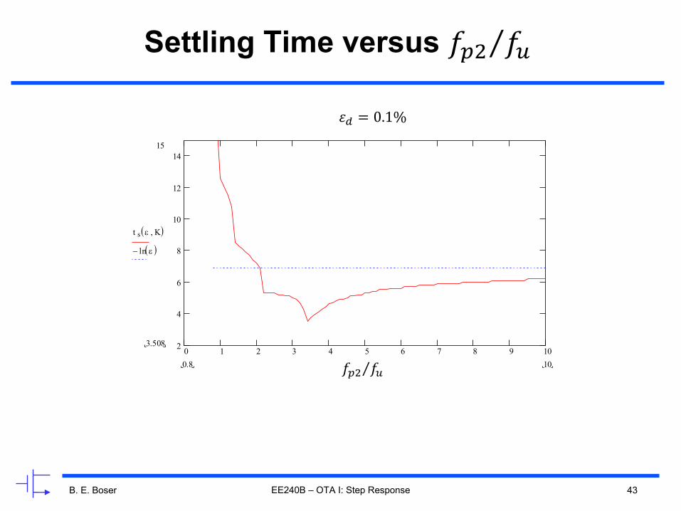
Settling Time versus 𝑓 " 𝑓R⁄
EE240B – OTA I: Step Response
0 1 2 3 4 5 6 7 8 9 102
4
6
8
10
12
1415
3.508
t s e K,( )
ln e( )-
100.8 K𝑓 " 𝑓R⁄
𝜀f = 0.1%

B. E. Boser 44
Noise
EE240B – OTA I: Step Response
[ B. Murmann ]

B. E. Boser 45
Advanced Analog Integrated Circuits
Design Example
Bernhard E. BoserUniversity of California, Berkeley
Copyright © 2016 by Bernhard Boser
EE240B – OTA I: Step Response
B. E. Boser 46
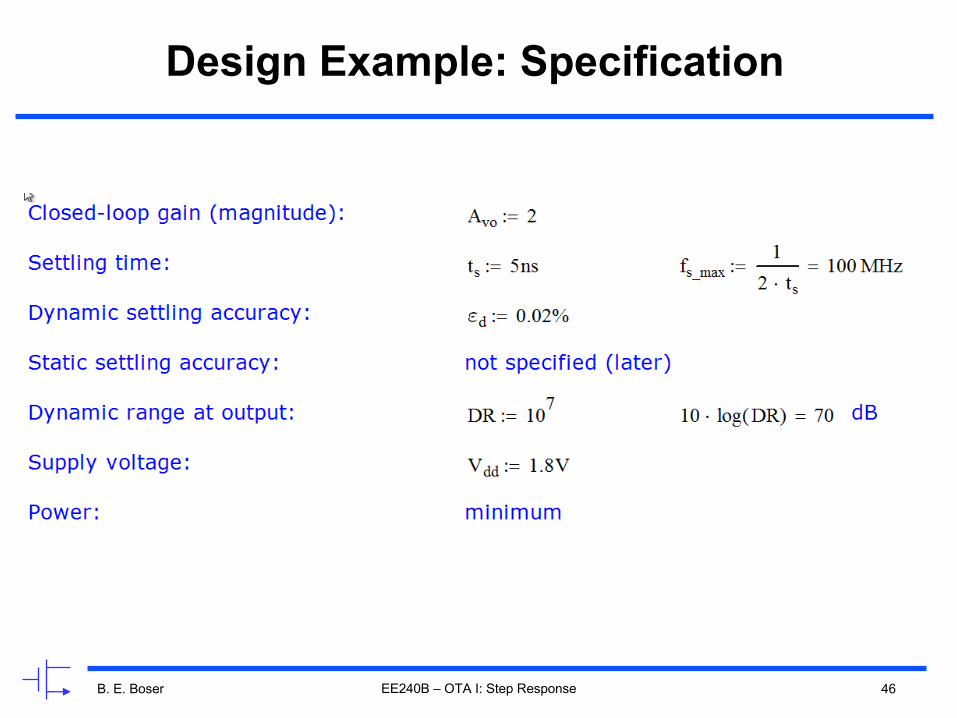
Design Example: Specification
EE240B – OTA I: Step Response
B. E. Boser 47
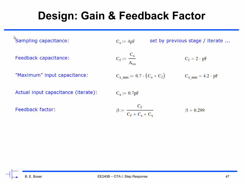
Design: Gain & Feedback Factor
EE240B – OTA I: Step Response
B. E. Boser 48
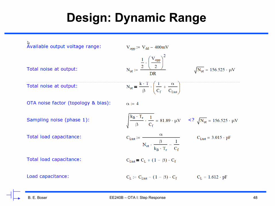
Design: Dynamic Range
EE240B – OTA I: Step Response

B. E. Boser 49
Design: Settling
EE240B – OTA I: Step Response

B. E. Boser 50
Design: Power Dissipation
EE240B – OTA I: Step Response

B. E. Boser 51
Could we go Faster?
EE240B – OTA I: Step Response
B. E. Boser 52
Advanced Analog Integrated Circuits
Gain Boosting
Bernhard E. BoserUniversity of California, Berkeley
Copyright © 2016 by Bernhard Boser
EE240B – OTA I: Step Response
B. E. Boser 53
Openloop Gain
𝑎H6 = 𝑔1𝑅6
EE240B – OTA I: Step Response
B. E. Boser 54
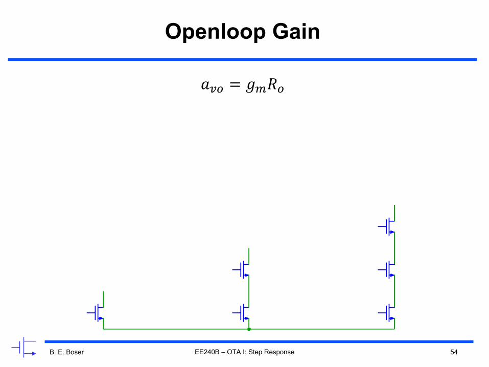
Openloop Gain
𝑎H6 = 𝑔1𝑅6
EE240B – OTA I: Step Response

B. E. Boser 55
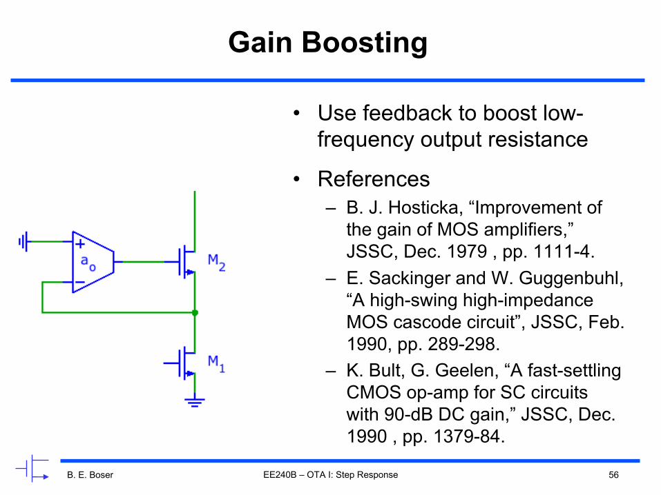
Gain Boosting
EE240B – OTA I: Step Response
B. E. Boser 56
Gain Boosting
• Use feedback to boost low-frequency output resistance
• References– B. J. Hosticka, “Improvement of
the gain of MOS amplifiers,” JSSC, Dec. 1979 , pp. 1111-4.
– E. Sackinger and W. Guggenbuhl, “A high-swing high-impedance MOS cascode circuit”, JSSC, Feb. 1990, pp. 289-298.
– K. Bult, G. Geelen, “A fast-settling CMOS op-amp for SC circuits with 90-dB DC gain,” JSSC, Dec. 1990 , pp. 1379-84.
EE240B – OTA I: Step Response
B. E. Boser 57
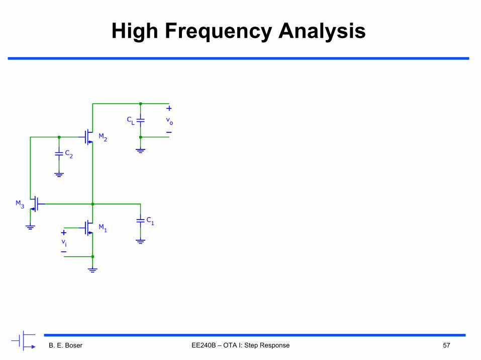
High Frequency Analysis
EE240B – OTA I: Step Response

B. E. Boser 58
Overall Amplifier Response
EE240B – OTA I: Step Response
Ref: M. Das, “Improved design criteria of gain boosted CMOS OTA with high-speed optimizations,” IEEE CAS II, March 2002, pp. 204-7.
𝜔]
𝜔6
𝑣6𝑣\
𝑓
Doublet

B. E. Boser 59
Advanced Analog Integrated Circuits
Pole-Zero Doublets
Bernhard E. BoserUniversity of California, Berkeley
Copyright © 2016 by Bernhard Boser
EE240B – OTA I: Step Response

B. E. Boser 60
Pole-Zero Doublets
Ref: Y. Kamath, R. G. Meyer, and P. R. Gray, “Relationship between frequency response and settling time of operational amplifiers,” IEEE J. Solid-State Circuits, pp. 347–352, Dec. 1974.
EE240B – OTA I: Step Response
B. E. Boser 61
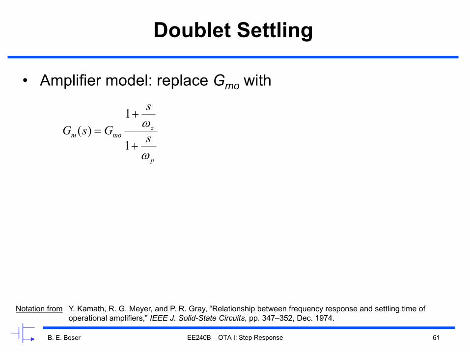
Doublet Settling
• Amplifier model: replace Gmo with
EE240B – OTA I: Step Response
p
zmom s
s
GsG
w
w
+
+=
1
1)(
Notation from Y. Kamath, R. G. Meyer, and P. R. Gray, “Relationship between frequency response and settling time of operational amplifiers,” IEEE J. Solid-State Circuits, pp. 347–352, Dec. 1974.

B. E. Boser 62
Doublet Settling
• Amplifier model: replace Gmo with
• Closed-loop response
EE240B – OTA I: Step Response
p
zmom s
s
GsG
w
w
+
+=
1
1)(
( )
1 h wit1
of bandwidth is , 33
<<+=
=
= --
eeaaw
w
wbww
pz
dBdBp sT
with
( ) ÷÷÷÷
ø
ö
çççç
è
æ
+
+
+-@
+-=
- pp
z
dBm
Leffin
o
s
s
sc
sFGC
sc
VV
w
w
w1
1
11
1
3ppp
Leff
modB C
FG
ww
w
@
=-3with
Notation from Y. Kamath, R. G. Meyer, and P. R. Gray, “Relationship between frequency response and settling time of operational amplifiers,” IEEE J. Solid-State Circuits, pp. 347–352, Dec. 1974.
B. E. Boser 63
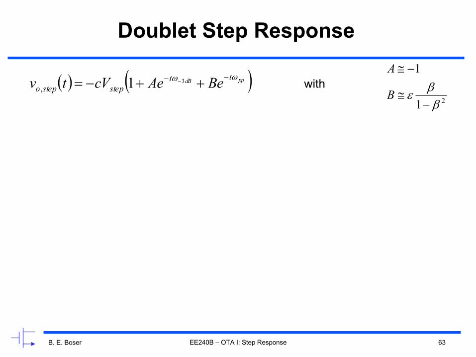
Doublet Step Response
EE240B – OTA I: Step Response
( ) ( )ppdB ttstepstepo BeAecVtv ww -- ++-= -31,
21
1
bbe-
@
-@
B
Awith
B. E. Boser 64
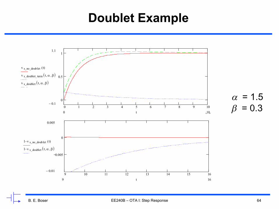
Doublet Example
EE240B – OTA I: Step Response
0 1 2 3 4 5 6 7 8 9 10
0
0.5
11.1
0.1-
v s_no_doublet t( )
v s_doublet_ term t a, b,( )
v s_doublet t a, b,( )
100 t
9 10 11 12 13 14 15 16
0.005
0
0.005
0.01-
1 v s_no_doublet t( )-
1 v s_doublet t a, b,( )-
169 t
a = 1.5b = 0.3
B. E. Boser 65
Gain Boosting – Doublets
EE240B – OTA I: Step Response