Embed Size (px)
Citation preview

Advanced Design SystemAdvanced Design System
Guan-Sung Li

ADS IntroductionADS Basic SimulationADS MomentumExample

ADS Windows
•Main Window•Schematic Window•Layout Window•Data Display Window
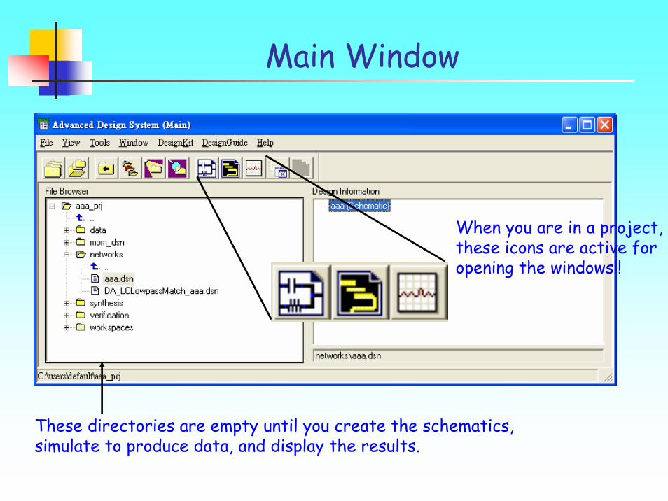
Main Window
These directories are empty until you create the schematics,simulate to produce data, and display the results.
When you are in a project,these icons are active foropening the windows!!

Create A New Project
Greeting dialog
Create new project command or icon
Menu commandsToolbar icons

Archive Project & UnArchive Project
•Archive files become *.zap files.•They can include all networks, data,and display files.
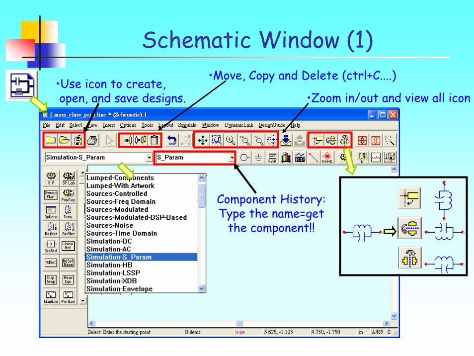
Schematic Window (1)
•Use icon to create,open, and save designs. •Zoom in/out and view all icon
•Move, Copy and Delete (ctrl+C....)
Component History:Type the name=get
the component!!

Schematic Window (2)
Insert VAR:Variable Equation
Activate/Deactivatetoggle icon
Insert Wire/Pin Label
Edit components to seeand modify parametervalues.

Push/Pop For Sub-circuits

Component Library
Select the part and it isattached to your cursor,
ready to insert.
FIND and part of searchthe Internet for parts.

Design kits – Install

Design kits - Murata ComponentMurata
component
LWQ18A series

ADS IntroductionADS Basic SimulationADS MomentumExample

Basic Simulation Flow (S_Parameter)
Create a schematic
Simula
te
Display Data
Simulation Status Window:Simulation info: message, error, etc…
Simulation controller
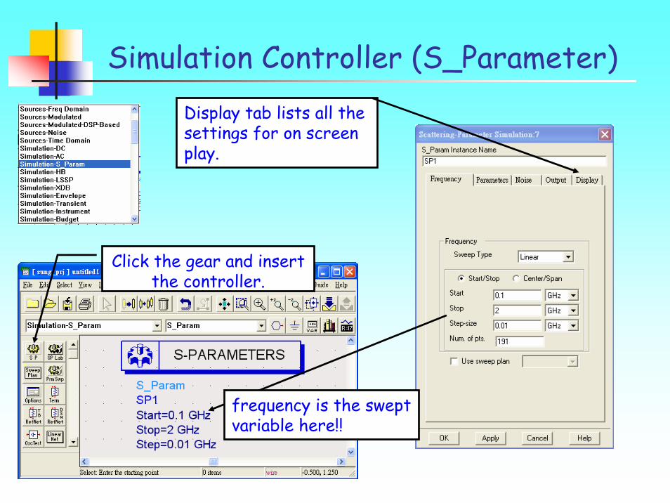
Simulation Controller (S_Parameter)
Click the gear and insert the controller.
frequency is the sweptvariable here!!
Display tab lists all the settings for on screen play.

Data ItemThe 1-port S-parameters are assumed to be measured with pin 1 as the input, and pin 2 (Ref) as the common terminal.
• The Ref node is normally grounded.
8720ESData format:*.f1
• File Type:1.Touchstone2.Datasat3.CITI-file4.Value

Simulation Information: Status Window
If there is a warning,it will appear here!!
One way to stop a simulation, click:Simulation/Synthesis>Stop Simulation
A successful simulation results in a dataset

Data Display Window (1)
Data Marker
Zoom in/out

Data Display Window (2)
Steps:(1) Insert the plot, list or equation.(2) Select the data or equations.(3) Trace Option – edit data or plot(4) Save/name the DDS windows.

Export Data (SNP)

Export Data (Data)

ADS ToolTuning Parameters (1)

ADS ToolTuning Parameter (2)

ADS ToolSmart Simulation Wizard (1)
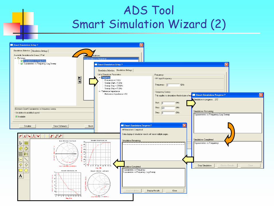
ADS ToolSmart Simulation Wizard (2)

ADS ToolSmith Char Utility

ADS ToolLineCalc

ADS IntroductionADS Basic SimulationADS MomentumExample

Momentum Process
ADSInterface
MOMInterface
1-a. Schematic with artwork1-b. Layout artwork2. Define the substrate3. Mesh and Solve4. Display

Creating a Layout from Schematic
•Schematic components must have artwork that can transfer to layout.•If not, draw the geometry or import the artwork into ADS layout.
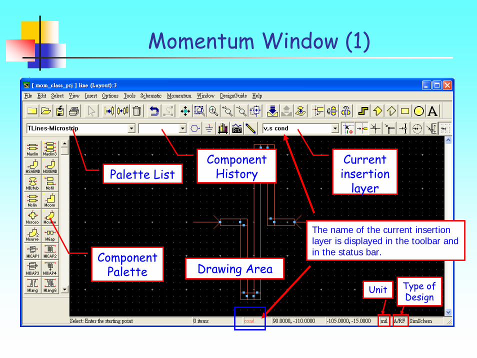
Momentum Window (1)
Component Palette
Palette ListComponent
HistoryCurrent insertion
layer
Drawing Area
The name of the current insertionlayer is displayed in the toolbar and in the status bar.
Unit Type ofDesign

Momentum Window (2)In a Layout window, this is done by placing a trace between the component (in the same way a wire is used in the Schematic window).
With each shape, you can either click and drag to place it, or define points by coordinate entry (choose the shape, then choose Insert > Coordinate Entry).
Snap toolbar
Use the Layers window, that is opened when a Layout window is opened andselect a name in the list of currently defined layers.

Layout Window
After the geometry and ports are in place, you areready to use these commands:• Enable regular Momentum or Momentum RF.• Substrate layer and metal/slot/via layer definitions.• Port type and impedance settings.• Mesh patterns defined and cleared.•Simulation S-parameter setups, including datasets.•Visualize currents and radiation patterns.•Save files for use in a 3D tool.

Selecting the Correct Mode
• Use Momentum (microwave) mode for designs requiring full-wave electromagnetic simulations that “include microwave radiation effects”.
• You might also choose Momentum RF mode for quick simulations on new microwave models that can “ignore radiation effects”, and to conserve computer resources.
Momentum Mode

Substrate• This is provides information about creating, modifying and editing a substrate.
※Choose Momentum > Substrate > Update From Schematic to update a substrate under the following conditions:
• You have used a substrate component on a schematic, such as MSUB or SSUB.
• You have already generated a layout from the schematic using Layout > Generate/Update Layout
• If you intend to precompute a mesh before you simulate, you must precomputethe substrate first.
※The steps for defining a substrate include: • Defining the substrate layers• Mapping the layout layers to metallization layers
• Specifying metallization layer conductivity• Solving the substrate

Substrate Create/Modify※A substrate definition is made up of “substrate layers”
and “metallization layers”:• Substrate layers define the dielectric media, ground planes,
covers, air or other layered material.
• Metallization layers are the conductive layers in between the substrate layers, and they are used in conjunction with the layout layers.
Substrate 1
Substrate 2
Air
Ground
Substrate Layers
Strip (metal) or slot (located at the interface of two substrates)
Strip (metal) or slot
Via extends through substrate
Metallization Layers

Defining Interface Layer (Substrate Layer)
※If this is a new definition, three default layers appear in the Substrate Layers Field:
• Free_space (top plane)• Alumina (dielectric)• GND (bottom plane)
permittivity of all dielectrics is assumed to becomplex:
which can also be expressed as:
where is the real portion of and is the dielectric loss tangent.
Permittivity(ε) format
Permeability(μ)format
Open Boundary (finite)
Closed Boundary (0)

Defining Interface Layer (Metallization Layers)1. Select the Substrate interface -------
and then select the layout drawing layer(metal drawing layer).
3. Specify Strip or Slot between 2 interfaces or a Via through a substrate layer.
2. Specify the Type, Thickness and Conductivity.

Via Simulation Models※There are three simulation models available for via objects in Momentum : • 2D Distributed Model• Lumped Model (ADS 2006A)• 3D Distributed Model (ADS 2006A)
※ Lumped Model :• The self and mutual capacitances are NOT included.• The mutual inductances are NOT included.• Frequency dependent skin effects are NOT included.
※ 2D Distributed Model :• Only the vertical component of the via current is modeled.• using vertical oriented rooftop functions. • The via self and mutual inductances. (vertical currents only)
and capacitances are included in the simulation.
※ 3D Distributed Mode : • Both the horizontal and vertical components of the via
current are modeled, using horizontal and vertical oriented rooftop functions.
• The via resistance and skin effect are included using the surface impedance formulation.
• All the via self and mutual inductances and capacitances are included in the simulation.

3D Expansion For Thick Conductors
• Conductors with finite thickness can be modeled in Momentum using the 3D metal expansion feature.
• Use Thick conductor when Height/Width ratio > a factor of 5.• Does not work for slot layers.• Thick metal increases the simulation time.

Overlap Precedence
• Overlap precedence specifies which layout layer has precedence over another if two or more layout layers are assigned to the same metallization layer and objects on the metallization layer overlap.
• If you do not set the precedence, and there are overlapping objects, a mesh will automatically and arbitrarily be created, with no errors reported.
• Precedence affects only how the mesh is created, it does not affect or alter the layout layers in your design.
Precedence = 1 Precedence =2
Overlap removed, geometry of object on toplayer is altered

Example: Via Fed Patch Antenna (1)Air
Alumina_112.5
Alumina_012.5
Cond = stripHole = viaCond2 = strip
Ground
Add
Define Substrate Layer
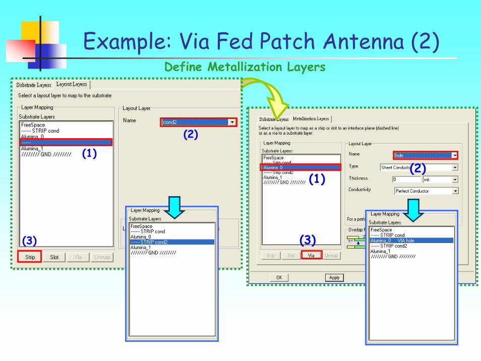
Example: Via Fed Patch Antenna (2)
(1)(2)
(3)
(1)
(2)
(3)
Define Metallization Layers
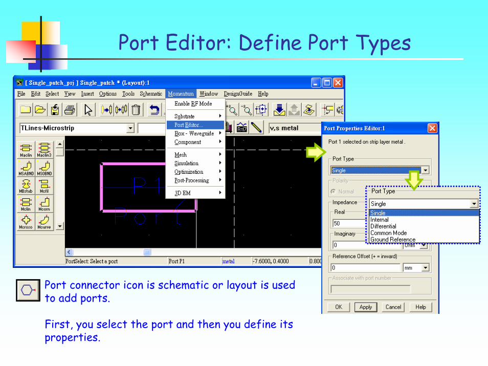
Port Editor: Define Port Types
Port connector icon is schematic or layout is used to add ports.
First, you select the port and then you define its properties.

Mesh
• In general, small patterns are more accurate but take more time to solve.
• You can choose not to set up mesh parameters, and default values will be used to create the mesh.
• Horizontal side current mesh canbe visualized.
• More accuracy for thick metal.
Mesh Frequency and cells/wavelengthare used in combination in determining mesh density.
Mesh reduction converts some Rectangles and triangles to polygons for fewer currents to solve.
※ Type of Mesh:1. Global Mesh
(The entire circuit)2. Layer Mesh:
(The objects on a layout layer)3. Primitive Mesh:
(A single object)
•If this is enabled, the geometry will be altered to produce a more accurate model for the overlap region.

Global Mesh With Edge Mesh
• The cell size is the same for all parts of thegeometry, except for the edges around eachprimitive.
1 - Port2 - Calibration Line3 - Mesh4 - Edge Mesh
The calibration line is automatically drawnwhen the port is defined.
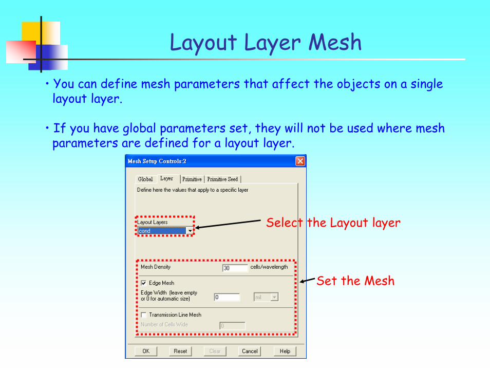
Layout Layer Mesh• You can define mesh parameters that affect the objects on a single layout layer.
• If you have global parameters set, they will not be used where mesh parameters are defined for a layout layer.
Select the Layout layer
Set the Mesh

Primitive Mesh With Edge MeshThe center primitive of this geometry has a different mesh density (50 cells/wavelength) than the two outside geometries (20 cells/wavelength).
In the Layout window, select the object that you want to specify mesh parameters for.

Primitive Seed Mesh
Primitive seeding enables you to specify the exact number of cells to be applied to a geometry:• Horizontally, across the O,U-axis• Vertically, from point V to the O,U-axis
Select the primitive you want to seed.
Draw U axis.
O U Identify point V
V
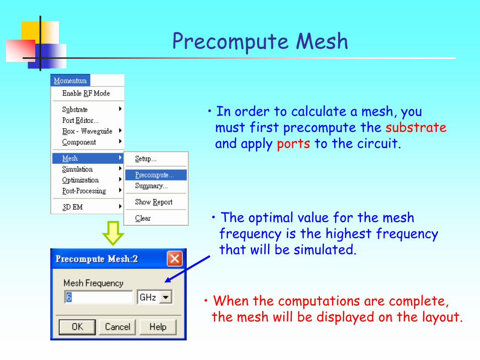
Precompute Mesh
• In order to calculate a mesh, you must first precompute the substrateand apply ports to the circuit.
• The optimal value for the mesh frequency is the highest frequency that will be simulated.
• When the computations are complete, the mesh will be displayed on the layout.

Simulate the Circuit (1)
※ Prior to running a simulation, the following criteria must be met:• A substrate definition must be specified
for the circuit.• The circuit must include at least one port.• The mesh is automatically calculated when
you simulate.• A simulation frequency plan must be
specified.
※ If any one of the above criteria is not met, Momentum will report an error if you try to run a simulation.

Simulate the Circuit (2)※ The steps for performing a simulation include:
(1) Specifying and editing frequency plans.(2) Selecting a process mode.(3) Specifying solution files.(4) Electing to view data.(5) Running the simulation.
※Process Mode:• The Foreground mode will pause a
simulation if the substrate has not yet been precomputed.
• The Background mode automatically precomputes the substrate if necessary.
• When the queue is running in normal operation (queue connected), the first waiting job will automatically start after the current job finishes.
(1)
(2)
(5)(3) (4)

Momentum Visualization (1)
※ You can display these types of data in Momentum Visualization:• S-parameters• Currents• far-fields• Antenna parameters• Transmission line data
• You can view the simulation results from any Momentum or Agilent HFSS project.
Menu Bar
Data editing
controls
Data on the plot
Selected plot
Plot editing
controls

Momentum Visualization (2)Current density
Without ‘Far Field’ menu

Momentum Visualization (3)
• You also have the option to look at the animated currents when click on the Display Properties button.
Antenna Parameters Animate
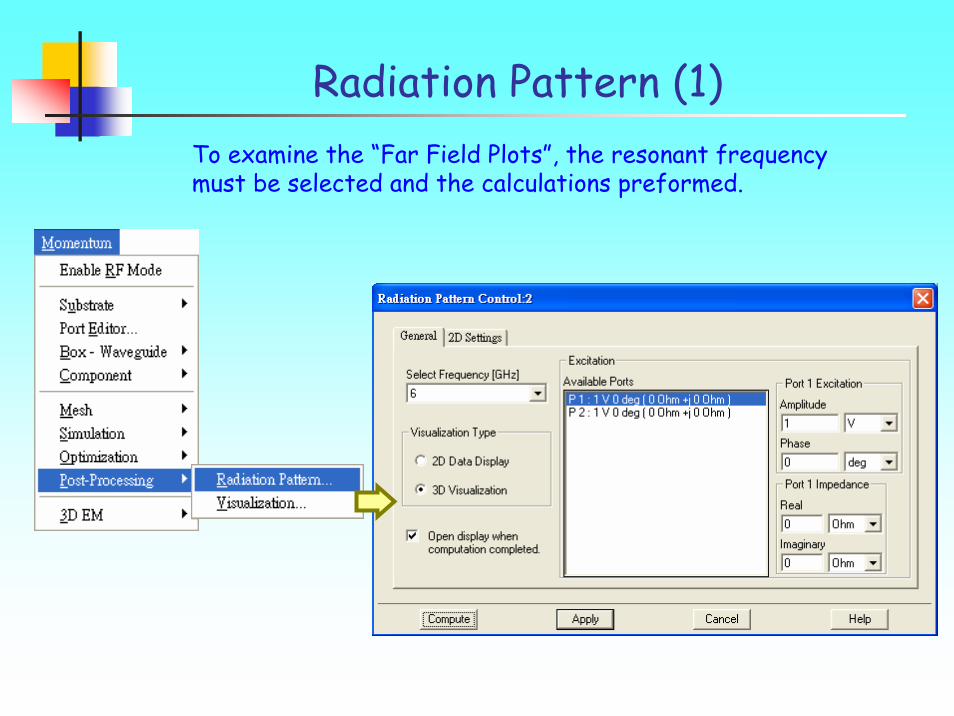
Radiation Pattern (1)To examine the “Far Field Plots”, the resonant frequencymust be selected and the calculations preformed.

Radiation Pattern (2)

ADS IntroductionADS Basic SimulationADS MomentumExample
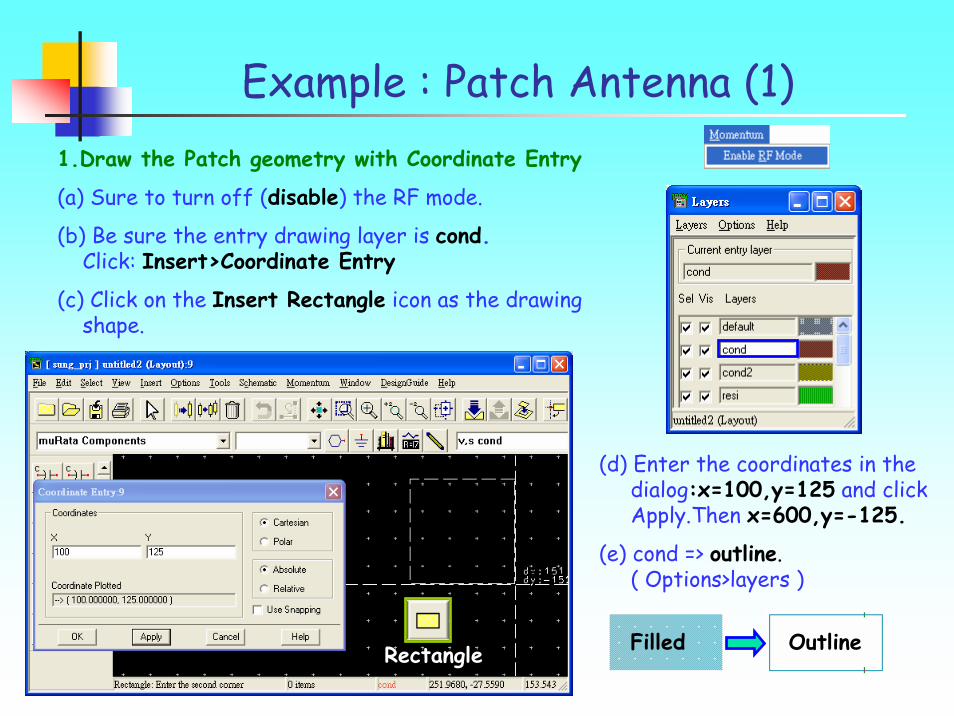
Example : Patch Antenna (1)1.Draw the Patch geometry with Coordinate Entry
(a) Sure to turn off (disable) the RF mode.
(b) Be sure the entry drawing layer is cond.Click: Insert>Coordinate Entry
(c) Click on the Insert Rectangle icon as the drawing shape.
(d) Enter the coordinates in thedialog:x=100,y=125 and clickApply.Then x=600,y=-125.
(e) cond => outline.( Options>layers )
OutlineFilledRectangle

Example : Patch Antenna (2)2.Draw the microstrip feed on another layer
a) Change the drawing layer to cond2.
b) Draw a Rectangle using coordinate entry.( x=0,y=5 and x=320,y=-5)
(1) (2)0,5
320,-5

Example : Patch Antenna (3)3.Draw the Via
(a) Set the entry drawing layer to hole.
(b) Verify that Vertex Snap mode is enabled.
(c) Select Polyline icon, then click to draw the via.
(2)
(1)
(3)
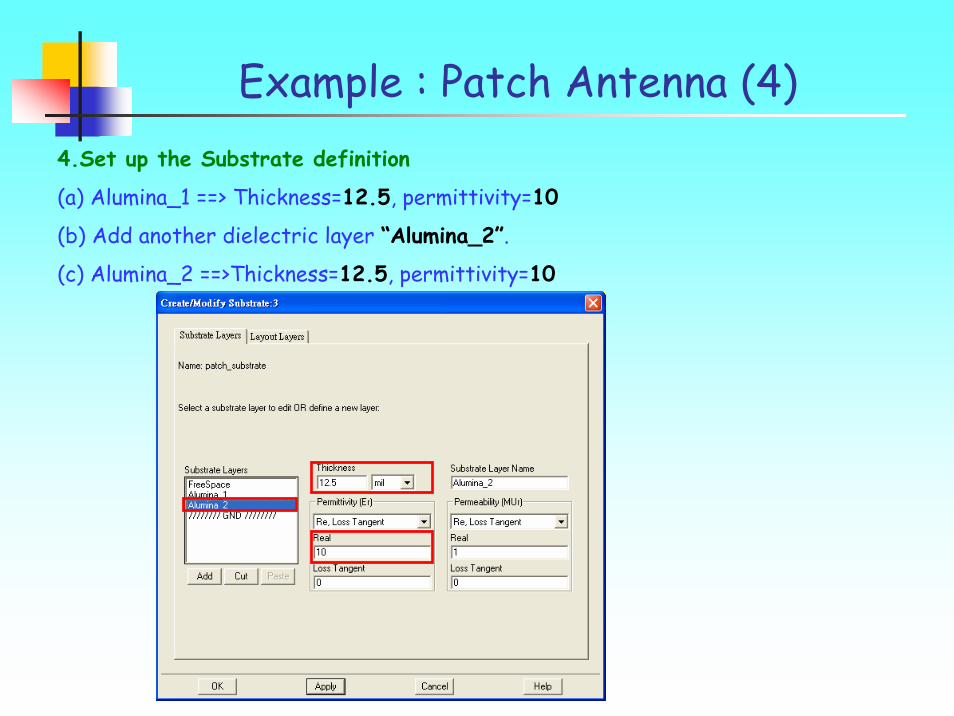
Example : Patch Antenna (4)4.Set up the Substrate definition
(a) Alumina_1 ==> Thickness=12.5, permittivity=10
(b) Add another dielectric layer “Alumina_2”.
(c) Alumina_2 ==>Thickness=12.5, permittivity=10

Example : Patch Antenna (5)5. Map the Strip Metalization layers to the substrate(a) Select the Metallization layers tab.(b) The cond layout layer should be mapped to Alumina_1 as a Strip.(c) Select the dashed line between the Alumina_1 and Alumina_2 substrates.(d) Click on strip to map cond2 as Strip between the two substrate layers.
(1)
(2)
(3)

Example : Patch Antenna (6)6.Map the Via through the substrate
(a) Select the Layout Layer hole.
(b) Click the Via button.
(c) Click Momentum > Substrate > Save As.
(3)
(1)
(2)

Example : Patch Antenna (7)7.Precompute the substrate
(a) Click Momentum > Substrate > Precompute.
(b) Frequency ==> 1GHz to 10GHz.

Example : Patch Antenna (8)8.Add a Port to the feed line
(a) The entry drawing layer must be set to cond2 (input).
(b) Select the Toggle Midpoint Snap Mode icon to snap the center of the edge of the rectangle.
(c) Select Port icon, and add a port to feedline left end.
(3)(1)
(2)
(4)

Example : Patch Antenna (9)9.Define the Port
(a) Click on Momentum > Port Editor.
(b) Select the port on the layout window.
(c) Define the Port Type ==> Single.Impedance ==> 50.

Example : Patch Antenna (10)10.Mesh separate Layers• Feedline (cond2) ==> use Edge Mesh. (All high frequency)• Patch (cond) ==> Edge Mesh is not required. (Not have much current density)
(a) Click Momentum > Mesh> Setup.Set the frequency ==> 10GHz (Global tab)
(b) Select the Layer tab.Set the Mesh Density: cond ==> 20 cells/wavelength. (Edge Mesh off)
cond2 ==> 30 cells/wavelength. (Edge Mesh on)
(c) Click Momentum > Mesh > Precompute.

Example : Patch Antenna (11)11.Set up Simulation and solve
(a) Frequency sweep Type = Adaptive,start = 1GHz, stop = 10GHz, Sample Points Limit = 25,
(b) Simulate!!!
(1)
(3)
(2)

Example : Patch Antenna (12)12.Plot the simulation results
freq (1.000GHz to 10.00GHz)
m1
S11
m1freq=patch_OK_mom_a..S(1,1)=0.145 / -5.932impedance = Z0 * (1.335 - j0.041)
3.862GHz
2 3 4 5 6 7 8 91 10
2
4
6
8
0
10
freq, GHz
VS
WR
1
m1
m1freq=VSWR1=1.187Min
3.860GHz
2 4 6 80 10
-20
-15
-10
-5
-25
0
Frequency
Mag
. [dB
]
m1
S11
m1freq=dB(patch_OK_mom..S(1,1))=-21.344Min
3.860GHz

Example : Patch Antenna (13)13.Plot the Far Field Radiation Pattern-Visualization
(1) Click Momentum > Post-Processing > Radiation Pattern,
(2) Select the frequency.(resonance frequency)
(3) Compute!!!!
(4) Click Far Filed > Far Field Plot.

Example : Patch Antenna (14)

T h a n k s ! !T h a n k s ! !
专注于微波、射频、天线设计人才的培养 易迪拓培训 网址:http://www.edatop.com
射 频 和 天 线 设 计 培 训 课 程 推 荐
易迪拓培训(www.edatop.com)由数名来自于研发第一线的资深工程师发起成立,致力并专注于微
波、射频、天线设计研发人才的培养;我们于 2006 年整合合并微波 EDA 网(www.mweda.com),现
已发展成为国内最大的微波射频和天线设计人才培养基地,成功推出多套微波射频以及天线设计经典
培训课程和 ADS、HFSS 等专业软件使用培训课程,广受客户好评;并先后与人民邮电出版社、电子
工业出版社合作出版了多本专业图书,帮助数万名工程师提升了专业技术能力。客户遍布中兴通讯、
研通高频、埃威航电、国人通信等多家国内知名公司,以及台湾工业技术研究院、永业科技、全一电
子等多家台湾地区企业。
易迪拓培训课程列表:http://www.edatop.com/peixun/rfe/129.html
射频工程师养成培训课程套装
该套装精选了射频专业基础培训课程、射频仿真设计培训课程和射频电
路测量培训课程三个类别共 30 门视频培训课程和 3 本图书教材;旨在
引领学员全面学习一个射频工程师需要熟悉、理解和掌握的专业知识和
研发设计能力。通过套装的学习,能够让学员完全达到和胜任一个合格
的射频工程师的要求…
课程网址:http://www.edatop.com/peixun/rfe/110.html
ADS 学习培训课程套装
该套装是迄今国内最全面、最权威的 ADS 培训教程,共包含 10 门 ADS
学习培训课程。课程是由具有多年 ADS 使用经验的微波射频与通信系
统设计领域资深专家讲解,并多结合设计实例,由浅入深、详细而又
全面地讲解了 ADS 在微波射频电路设计、通信系统设计和电磁仿真设
计方面的内容。能让您在最短的时间内学会使用 ADS,迅速提升个人技
术能力,把 ADS 真正应用到实际研发工作中去,成为 ADS 设计专家...
课程网址: http://www.edatop.com/peixun/ads/13.html
HFSS 学习培训课程套装
该套课程套装包含了本站全部 HFSS 培训课程,是迄今国内最全面、最
专业的HFSS培训教程套装,可以帮助您从零开始,全面深入学习HFSS
的各项功能和在多个方面的工程应用。购买套装,更可超值赠送 3 个月
免费学习答疑,随时解答您学习过程中遇到的棘手问题,让您的 HFSS
学习更加轻松顺畅…
课程网址:http://www.edatop.com/peixun/hfss/11.html
`

专注于微波、射频、天线设计人才的培养 易迪拓培训 网址:http://www.edatop.com
CST 学习培训课程套装
该培训套装由易迪拓培训联合微波 EDA 网共同推出,是最全面、系统、
专业的 CST 微波工作室培训课程套装,所有课程都由经验丰富的专家授
课,视频教学,可以帮助您从零开始,全面系统地学习 CST 微波工作的
各项功能及其在微波射频、天线设计等领域的设计应用。且购买该套装,
还可超值赠送 3 个月免费学习答疑…
课程网址:http://www.edatop.com/peixun/cst/24.html
HFSS 天线设计培训课程套装
套装包含 6 门视频课程和 1 本图书,课程从基础讲起,内容由浅入深,
理论介绍和实际操作讲解相结合,全面系统的讲解了 HFSS 天线设计的
全过程。是国内最全面、最专业的 HFSS 天线设计课程,可以帮助您快
速学习掌握如何使用 HFSS 设计天线,让天线设计不再难…
课程网址:http://www.edatop.com/peixun/hfss/122.html
13.56MHz NFC/RFID 线圈天线设计培训课程套装
套装包含 4 门视频培训课程,培训将 13.56MHz 线圈天线设计原理和仿
真设计实践相结合,全面系统地讲解了 13.56MHz线圈天线的工作原理、
设计方法、设计考量以及使用 HFSS 和 CST 仿真分析线圈天线的具体
操作,同时还介绍了 13.56MHz 线圈天线匹配电路的设计和调试。通过
该套课程的学习,可以帮助您快速学习掌握 13.56MHz 线圈天线及其匹
配电路的原理、设计和调试…
详情浏览:http://www.edatop.com/peixun/antenna/116.html
我们的课程优势:
※ 成立于 2004 年,10 多年丰富的行业经验,
※ 一直致力并专注于微波射频和天线设计工程师的培养,更了解该行业对人才的要求
※ 经验丰富的一线资深工程师讲授,结合实际工程案例,直观、实用、易学
联系我们:
※ 易迪拓培训官网:http://www.edatop.com
※ 微波 EDA 网:http://www.mweda.com
※ 官方淘宝店:http://shop36920890.taobao.com
专注于微波、射频、天线设计人才的培养
官方网址:http://www.edatop.com 易迪拓培训 淘宝网店:http://shop36920890.taobao.com