Embed Size (px)
Citation preview

Advanced materials and design for
board level EMI shielding
Colin Tong
Laird Technologies
1751 Wilkening Court, Schaumburg, IL 60173, USA
February 15, 2012
22
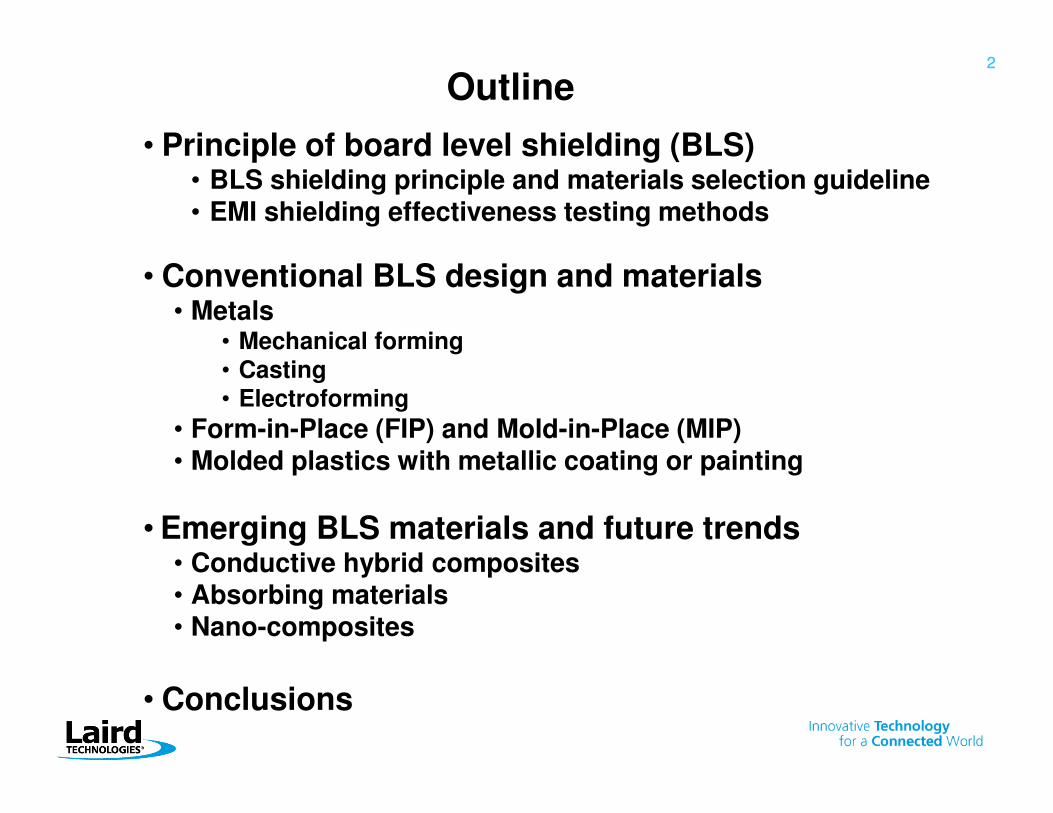
Outline
• Principle of board level shielding (BLS) • BLS shielding principle and materials selection guideline • EMI shielding effectiveness testing methods
• Conventional BLS design and materials• Metals
• Mechanical forming
• Casting
• Electroforming
• Form-in-Place (FIP) and Mold-in-Place (MIP) • Molded plastics with metallic coating or painting
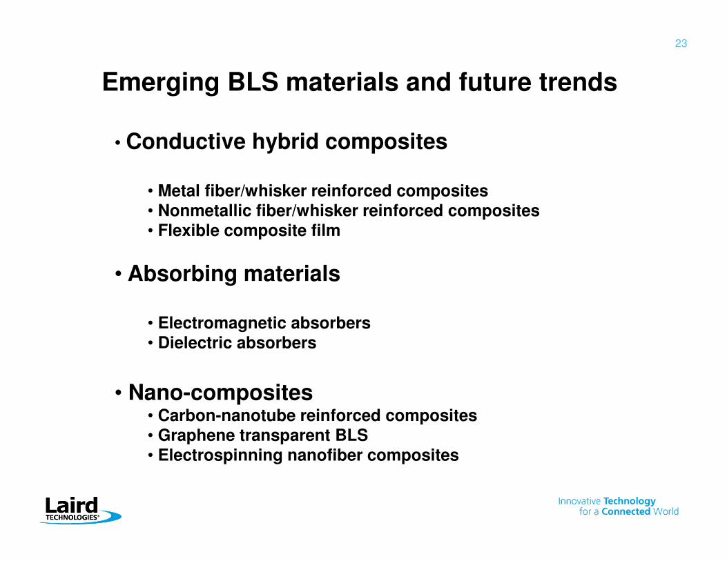
• Emerging BLS materials and future trends• Conductive hybrid composites• Absorbing materials• Nano-composites
• Conclusions

3
Basic principle of board level shielding
• Based on Faraday cage principle, BLS can be designed with different forms, depending on the application requirements and mounting methods.
Ventilation holes
Five-sided can
DC power filter
Mains filter
Signal filters for PCB tracks
PCB with ground plane
Typical 5 sided metal can is used to form 6 sided shield through the attachment /connection to the ground plane on PCB
Typical 5 sided metal can is used to form 6 sided shield through the attachment /connection to the ground plane on PCB
E[V/m]
Shell Equatorial plane
Equipment

4
• Major functions of BLS
• Shield different zones of a device
from each other
• Cover it – no inside EMI escape,
and no outside EMI entering
• Ground/seal it – no EMI leakage
• Manage system heat dissipation
• Minimize real estate used
• Minimize weight and cost
• Key factors for effective shielding
MATERIAL
• Electrical conductivity/permeability/
permittivity
• Wall thickness/surface coating
• Thermal conductivity
• Environmental compatibility
• Manufacturability
Geometry
• Holes
• Slots
• Gaps
Termination
• Shield-Board interface
• Connectivity
• Joining/Mounting methods
Cost usually dominates material selection for BLSCost usually dominates material selection for BLS
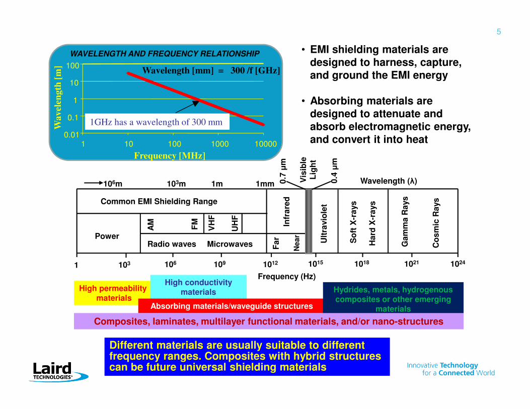
5
0.01
0.1
1
10
100
1 10 100 1000 10000
Frequency [MHz]
Wa
vel
ength
[m
]
1GHz has a wavelength of 300 mm
Wavelength [mm] = 300 /f [GHz]
WAVELENGTH AND FREQUENCY RELATIONSHIP
1 103 106 109 1012 1015 1018 1021 1024
Frequency (Hz)
PowerRadio waves Microwaves F
ar
Near
AM
FM
VH
F
UH
F
Infr
are
d
Ult
ravio
let
So
ft X
-ra
ys
Ha
rd X
-ra
ys
Ga
mm
a R
ays
Co
sm
ic R
aysCommon EMI Shielding Range
Vis
ible
L
igh
t
0.7
µm
0.4
µm
106m 103m 1m 1mm Wavelength (λ)
High permeability
materials
High conductivity materials
Absorbing materials/waveguide structures
Hydrides, metals, hydrogenous
composites or other emerging materials
Composites, laminates, multilayer functional materials, and/or nano-structures
Different materials are usually suitable to different frequency ranges. Composites with hybrid structures can be future universal shielding materials
Different materials are usually suitable to different frequency ranges. Composites with hybrid structures can be future universal shielding materials
• EMI shielding materials are
designed to harness, capture,
and ground the EMI energy
• Absorbing materials are
designed to attenuate and
absorb electromagnetic energy,
and convert it into heat
6
• EMI shielding principle of conductive materials
Reflection loss depends on the distance of the EMI source to the material (different for electric, magnetic, and plane waves), material electrical conductivity, and the frequency of the incident wave.
Reflection loss depends on the distance of the EMI source to the material (different for electric, magnetic, and plane waves), material electrical conductivity, and the frequency of the incident wave.
Incident WaveE0, H0
Transmitted WaveE1, H2
ReflectionLoss, R
AbsorptionLoss, A
Internal Reflection
Re-reflected
term
Second
Reflection loss
0 Distance from shield edge, t
Remaining field strength, E1, H1
E0, H0
37%E0, H0
Skin depth, δ
µ
σ23
log108.321rf
RE +=
µ
σ2
log106.14fr
RH +=
σ
µfRP log10168 −=
Where RE, RH, and RP are the reflection losses for the electric, magnetic, and plane wave fields expressed in dB; σ is the relative conductivity referred to copper; f is the frequency in Hz; µ is the relative permeability referred to free space; r is the distance from the source to the shielding in m.
SE = R +A +B

µσπδ
f
1=
E1=E0 e-t/δ, and H1=H0 e-t/δ. The distance required for the wave to be attenuated to 1/e or 37% is defined as the skin depth, δ.
• Absorption Loss
Absorption loss depends on material thickness, permeability, electrical conductivity, and the frequency of the incident wave. It is the same for all electromagnetic waves.
Absorption loss depends on material thickness, permeability, electrical conductivity, and the frequency of the incident wave. It is the same for all electromagnetic waves.
Where A is the absorption or penetration loss expressed in dB; t is the thickness of the shield in mm; f is frequency in MHz; µ is relative permeability (1 to copper); σ is conductivity relative to copper in %IACS.
µσfA = 20ln (t/δ) = 131 t
Frequency (Hz)
10 100 1000 1k 10k 100k 1M 10M 100M 1G 10G 100G
Min
imum
Thic
knes
s (m
m)
0.0001
0.001
0.01
0.1
1
10
100
Min
imum
Thic
knes
s (i
nch
es)
0.00001
0.0001
0.001
0.01
0.1
1
Copper Mild Steel
Aluminum StainlessSteel
Typical plating thickness
7
Armstrong, K. www.compliance-club.com
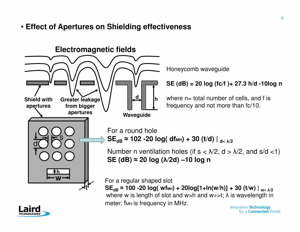
8
• Effect of Apertures on Shielding effectiveness
t
ds
wh
Electromagnetic fields
Shield with apertures
Greater leakage from bigger apertures
Waveguide
d h
Honeycomb waveguide
SE (dB) = 20 log (fc/f )+ 27.3 h/d -10log n
where n= total number of cells, and f is
frequency and not more than fc/10.
Number n ventilation holes (if s < λ/2, d > λ/2, and s/d <1)
SE (dB) ≈ 20 log (λ/2d) –10 log n
For a regular shaped slot
SEdB ≈ 100 -20 log( wfMH) + 20log[1+ln(w/h)] + 30 (t/w) | w< λ/2
where w is length of slot and w>h and w>>t; λ is wavelength in
meter; fMH is frequency in MHz.
For a round hole
SEdB ≈ 102 -20 log( dfMH) + 30 (t/d) | d< λ/2

9
Wrap Around Corner
Wavy Corner
• Example: Calculated shielding effectiveness difference with differentcorners
The longest dimension of the aperture limits or dominates the BLS shielding effectiveness. The longest dimension of the aperture limits or dominates the BLS shielding effectiveness.

• EMI shielding effectiveness testing methods
MIL-STD-285 – Shelters - WithdrawnNSA 65-6 and 73-2A – Shelter SE measurementsMIL-DTL-83528 – Conductive Elastomer EMI Gasket Radiated Field and DC Volume ResistivityIEEE STD 299 – Shelters (replaced MIL-STD-285)IEEE STD 1302 – Guide to EMI Gasket Test MethodsASTM D4935 – Planar Materials - WithdrawnASTM E1851 – Shelters (duplicates MIL-STD-285)SAE ARP 1705 – EMI Gasket Transfer ImpedanceSAE ARP 1173 – EMI Gasket Radiated FieldEN 50147-1/VDE 0876-147-3 – Enclosure SE MeasurementIEC 61000-5-7 – Enclosures Degree of ProtectionIEC 61000-4-21 – Reverberation Chamber Test TechniquesSCTE 48-1-2006 – GTEM Cell Tests
EMSCAN

11
• EMSCAN functionality and configuration
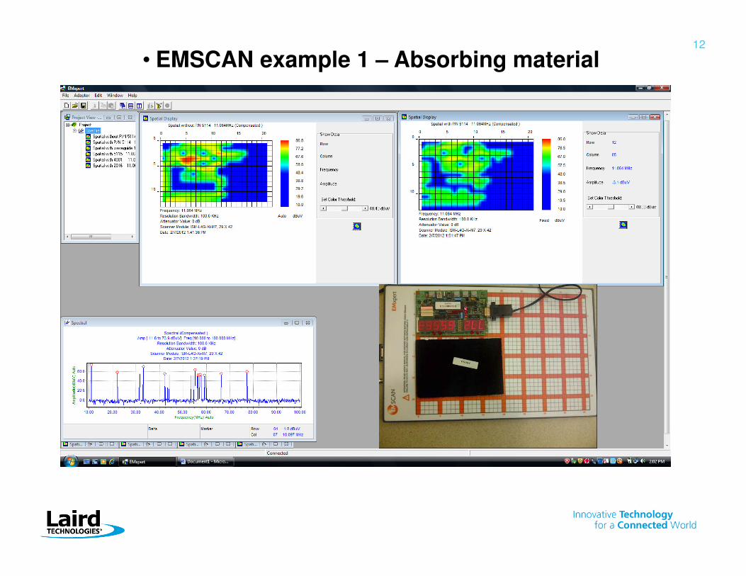
12
• EMSCAN example 1 – Absorbing material

13
• EMSCAN example 2 – Waveguide
14
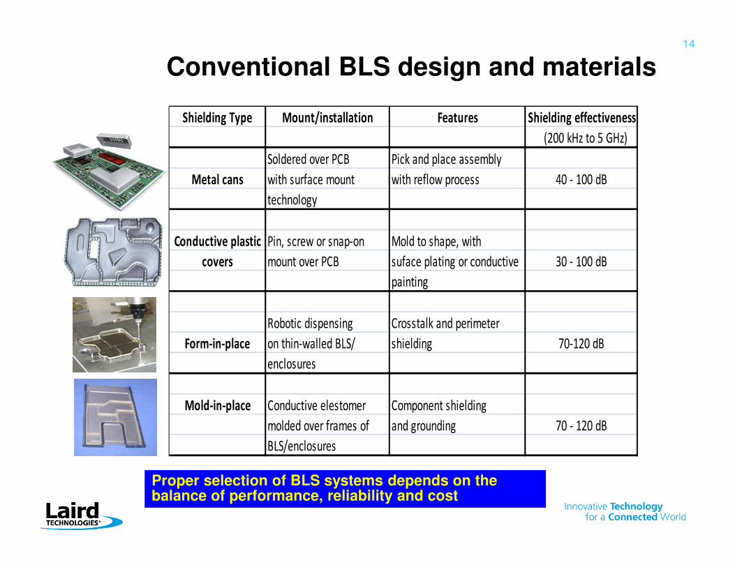
Conventional BLS design and materials
Proper selection of BLS systems depends on the balance of performance, reliability and costProper selection of BLS systems depends on the balance of performance, reliability and cost
Shielding Type Mount/installation Features Shielding effectiveness
(200 kHz to 5 GHz)
Soldered over PCB Pick and place assembly
Metal cans with surface mount with reflow process 40 - 100 dB
technology
Conductive plastic Pin, screw or snap-on Mold to shape, with
covers mount over PCB suface plating or conductive 30 - 100 dB
painting
Robotic dispensing Crosstalk and perimeter
Form-in-place on thin-walled BLS/ shielding 70-120 dB
enclosures
Mold-in-place Conductive elestomer Component shielding
molded over frames of and grounding 70 - 120 dB
BLS/enclosures

15
• Metals
• Mechanical forming
- Bending, stamping or drawing
- Tin plated CRS, SS, Al, or Cu alloys
- Nickel silver
• Cast Al, Mg or Zn
• Electroforming
Mechanically formed metal cans are the low cost and most common used BLS especially with high volume productionMechanically formed metal cans are the low cost and most common used BLS especially with high volume production
16
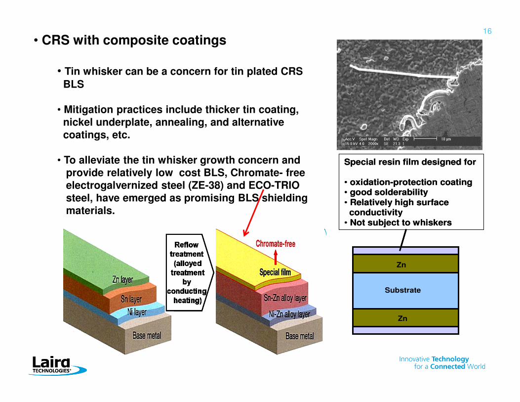
• CRS with composite coatings
• Tin whisker can be a concern for tin plated CRS
BLS
• Mitigation practices include thicker tin coating,
nickel underplate, annealing, and alternative
coatings, etc.
• To alleviate the tin whisker growth concern and
provide relatively low cost BLS, Chromate- free
electrogalvernized steel (ZE-38) and ECO-TRIO
steel, have emerged as promising BLS shielding
materials.
Substrate
Zn
Special resin film designed for
• oxidation-protection coating • good solderability
• Relatively high surface conductivity
• Not subject to whiskers
Zn
Substrate
Zn
Special resin film designed for
• oxidation-protection coating • good solderability
• Relatively high surface conductivity
• Not subject to whiskers
Zn
17
• Die casting for BLS/Enclosures
• Major advantages
- Durable, robust enclosure solution
- Match with environmental sealing (space gaskets, including FIP, MIP etc.)
- Good for thermal dissipation
• Disadvantages
- Heaviest BLS/enclosure ( minimum thickness 0.4 mm)
- Draft requirement means sloped sidewalls
- Die tooling cost is a major concern for small scale production
• Die casting materials typically include Al, Mg, and Zn
• Al has good corrosion resistance and mechanical properties, high
thermal and electrical conductivity, and strength at elevated
temperatures
• Zn is the easiest alloy to cast because of its low melting point, which is
economical for production of small BLS parts
• Mg is the lightest alloy in common use
18
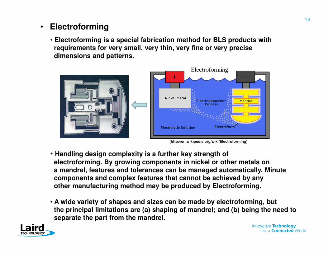
• Electroforming is a special fabrication method for BLS products with
requirements for very small, very thin, very fine or very precise
dimensions and patterns.
• Handling design complexity is a further key strength of
electroforming. By growing components in nickel or other metals on
a mandrel, features and tolerances can be managed automatically. Minute
components and complex features that cannot be achieved by any
other manufacturing method may be produced by Electroforming.
• A wide variety of shapes and sizes can be made by electroforming, but
the principal limitations are (a) shaping of mandrel; and (b) being the need to
separate the part from the mandrel.
• Electroforming
(http://en.wikipedia.org/wiki/Electroforming)
19
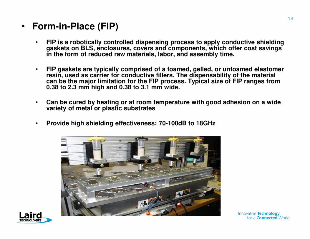
• Form-in-Place (FIP)
• FIP is a robotically controlled dispensing process to apply conductive shielding gaskets on BLS, enclosures, covers and components, which offer cost savings in the form of reduced raw materials, labor, and assembly time.
• FIP gaskets are typically comprised of a foamed, gelled, or unfoamed elastomerresin, used as carrier for conductive fillers. The dispensability of the material can be the major limitation for the FIP process. Typical size of FIP ranges from 0.38 to 2.3 mm high and 0.38 to 3.1 mm wide.
• Can be cured by heating or at room temperature with good adhesion on a wide variety of metal or plastic substrates
• Provide high shielding effectiveness: 70-100dB to 18GHz
20
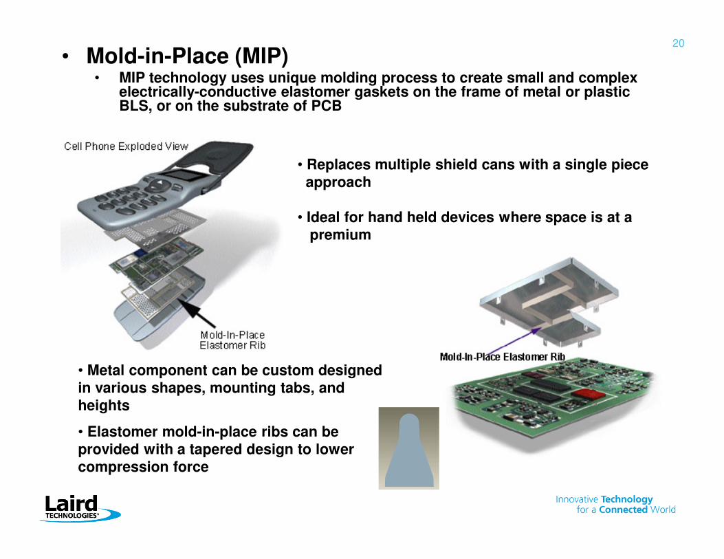
• Replaces multiple shield cans with a single piece
approach
• Ideal for hand held devices where space is at a
premium
• Metal component can be custom designed
in various shapes, mounting tabs, and
heights
• Elastomer mold-in-place ribs can be
provided with a tapered design to lower
compression force
• Mold-in-Place (MIP)• MIP technology uses unique molding process to create small and complex
electrically-conductive elastomer gaskets on the frame of metal or plastic BLS, or on the substrate of PCB
21
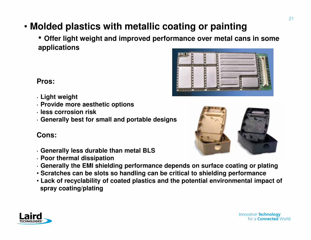
Pros:
· Light weight
· Provide more aesthetic options
· less corrosion risk
· Generally best for small and portable designs
Cons:
· Generally less durable than metal BLS
· Poor thermal dissipation
· Generally the EMI shielding performance depends on surface coating or plating
• Scratches can be slots so handling can be critical to shielding performance
• Lack of recyclability of coated plastics and the potential environmental impact of
spray coating/plating
• Molded plastics with metallic coating or painting
• Offer light weight and improved performance over metal cans in some
applications
22
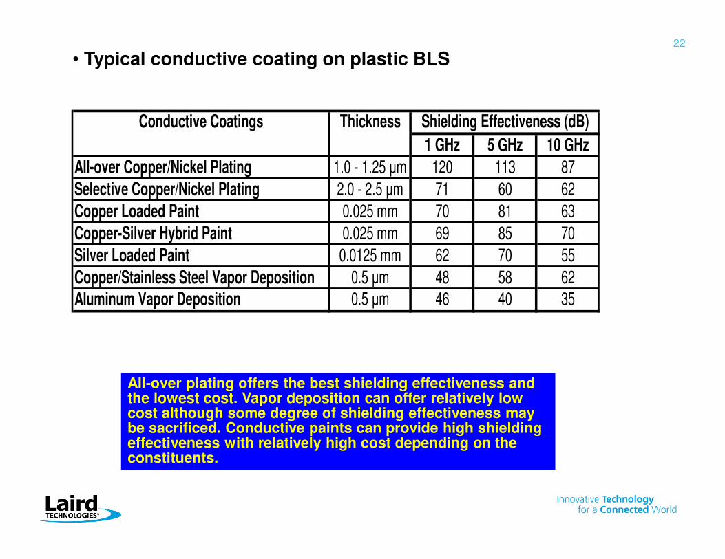
• Typical conductive coating on plastic BLS
Conductive Coatings Thickness
1 GHz 5 GHz 10 GHz
All-over Copper/Nickel Plating 1.0 - 1.25 µm 120 113 87
Selective Copper/Nickel Plating 2.0 - 2.5 µm 71 60 62
Copper Loaded Paint 0.025 mm 70 81 63
Copper-Silver Hybrid Paint 0.025 mm 69 85 70
Silver Loaded Paint 0.0125 mm 62 70 55
Copper/Stainless Steel Vapor Deposition 0.5 µm 48 58 62
Aluminum Vapor Deposition 0.5 µm 46 40 35
Shielding Effectiveness (dB)
All-over plating offers the best shielding effectiveness and the lowest cost. Vapor deposition can offer relatively low cost although some degree of shielding effectiveness may be sacrificed. Conductive paints can provide high shielding effectiveness with relatively high cost depending on the constituents.
All-over plating offers the best shielding effectiveness and the lowest cost. Vapor deposition can offer relatively low cost although some degree of shielding effectiveness may be sacrificed. Conductive paints can provide high shielding effectiveness with relatively high cost depending on the constituents.
23
Emerging BLS materials and future trends
• Conductive hybrid composites
• Metal fiber/whisker reinforced composites
• Nonmetallic fiber/whisker reinforced composites
• Flexible composite film
• Absorbing materials
• Electromagnetic absorbers
• Dielectric absorbers
• Nano-composites• Carbon-nanotube reinforced composites
• Graphene transparent BLS
• Electrospinning nanofiber composites

RTP 2799 S x 118601 B (TJ)
60
70
80
90
100
110
120
1.E+04 1.E+05 1.E+06 1.E+07 1.E+08 1.E+09
Frequency (Hz)
Sh
ield
ing
Eff
ec
tiv
en
es
s (
dB
)
2424
• Reinforcement or filler- Al, Cu, Fe, S.S., Ag, Ti, Co, Ni, Ti, W etc.
• Matrix - Selected polymer- Hydrogen-rich polymer- Rare-earth-doped rubber
2424
• Conductive hybrid composites• Optimal selection of reinforcements and base materials to get best
compatibility;
• Optimizing the layout of the reinforcements to maximize the percolation
effect
• Metal fiber/whisker reinforced composites
Absorbed wave
Incident wave
Reflected wave Transmitted
wave
Secondary reflections
Stainless steel fiber/whisker
reinforced composite

2525
• Nonmetallic fiber/whisker reinforced composites
• Reinforcement or filler
- Metal coated or Intercalated graphite fiber or foam; boron fiber;
Nanotube or nanofiber etc.
• Matrix
- Selected polymer
- Hydrogen-rich polymer
2525
Ni plated carbon
fiber with dispersion agent

262626
Reversed magnetic field from composite
Transparent film for
surface insulation (0.01 mm thick)
Flexible magnetic composite(0.1 mm thick)
Adhesive tape (0.01 mm thick)
Electrical power
High-speed signal line
Magnetic flux from
electric power & signal transmission
• Flexible composite film
• Ideal for thinning and weight saving of electronic devices in
communication industry

27
• Material absorption capability in an electromagnetic field
A (W/m3) = ½ σE2 + ππππfε0εRE2 + ππππfµ0µRH2
E(V/m) is electric field strength; H(A/m) is magnetic field strength; σ(S/m) is conductivity; f is frequency; ε0 (F/m) is permittivity of the vacuum; εR is complex permittivity; µ0[A/m] is permeability of the vacuum; µR is complex permeability.
• Absorption of EMI energy rely on the conductivity, dielectric loss and /or magnetic loss of the absorber material
• Dielectric loss is characterized as the complex permittivity (createdby carbon or other electrically conductive or capacitive particles) andacts on the electric field
• Magnetic loss is characterized as the complex permeability (magneticfillers - special irons and ferrites) and acts on the magnetic field
•Absorbing materials
Dielectric absorbing materialsDielectric absorbing materials
Magnetic absorbing materialsMagnetic absorbing materials

282828
Ferrite based absorber
30
20
10
0R
etu
rn lo
ss (
dB
)
10 100 1000
Frequency (MHz)
Plastic based
absorber
0 10 20
Frequency (MHz)
100
50
0
Att
en
ua
tio
n c
on
sta
nt
(dB
/cm
)
Ferrite Mortar
0 200 800
Frequency (MHz)400 600
10
20
30
Retu
rn lo
ss (
dB
)
0 5 20
Frequency (MHz)
10 15 25
Retu
rn lo
ss (
dB
)
0
10
20
30
40
50
Rubber based absorber
• Examples of magnetic absorbers
29
Incident radiation
Dielectric layer
Metal substrate
3.81mm
3.81mm
22.5°0.0762 mm max. radius
0.0254 mm
max. radius
• Example of some developing absorbers
• Far-infrared
radiation absorbing
Dallenbach like-
structure
• Submilimeter-wave
anechoic structure
• Hybrid structure
3030
Su
rface R
esis
tivit
y (
Oh
m)
0 10 20 30 40 50 60 70 80
Wt.% of Fillers
1018
1016
1014
1012
1010
108
106
104
102
0
Cu/PE
Al/PVC
VGCF/PP
SWNT/ABS
Insulation
ESD
EMIShielding
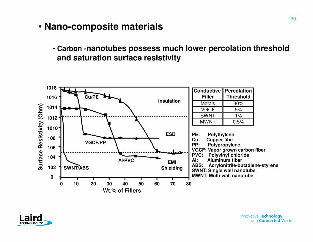
PE: PolythyleneCu: Copper fibePP: PolypropyleneVGCF: Vapor grown carbon fiberPVC: Polyvinyl chlorideAl: Aluminum fiberABS: Acrylonitrile-butadiene-styreneSWNT: Single wall nanotubeMWNT: Multi-wall nanotube
Conductive Percolation
Filler Threshold
Metals 30%
VGCF 5%
SWNT 1%
MWNT 0.5%
• Nano-composite materials
• Carbon -nanotubes possess much lower percolation threshold and saturation surface resistivity
3131
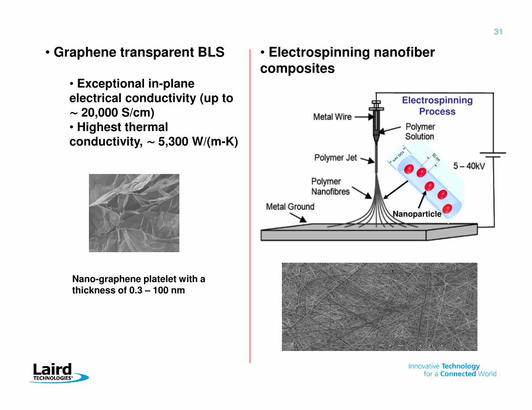
• Graphene transparent BLS
• Exceptional in-plane
electrical conductivity (up to
∼∼∼∼ 20,000 S/cm)
• Highest thermal
conductivity, ∼∼∼∼ 5,300 W/(m-K)
Nano-graphene platelet with a thickness of 0.3 – 100 nm
• Electrospinning nanofibercomposites
Nanoparticle
ElectrospinningProcess
32
Conclusions
• BLS can be the most cost- efficient means of solving EMI issues.
Materials selection, geometry design, and termination technology are
three key factors on the shielding performance.
• Tin plated CRS is the most common BLS material due mainly to
its excellent mechanical formability, high permeability, environmental
compliance, and relative low cost. The potential tin whisker growth
can be mitigated.
• To alleviate the tin whisker growth concern and provide relatively low
cost board-level shielding products, some environmentally friendly
composite plating steels, have emerged as promising board-level
shielding materials.
• Different materials are usually suitable to different frequency ranges.
Composites with hybrid structures can be future universal shielding
materials
• Nano-materials would play an important role for future BLS applications.

Thank You!