Embed Size (px)
Citation preview

i
ADVANCED QUANTUM MECHANICAL
TUNNELLING BASED DEVICES AND
AVALANCHE BREAKDOWN PHOTODIODES
FOR RADIO FREQUENCY AND OPTICAL
DETECTION SYSTEMS
A thesis submitted to The University of Manchester for the degree of
Doctor of Philosophy
In the Faculty of Science and Engineering
2019
Omar Saadallah Hamid Abdulwahid
Supervisor: Prof. Mohamed Missous
School of Electrical and Electronic Engineering

1
TABLE OF CONTENT
TABLE OF CONTENT ...................................................................................................... 1
LIST OF TABLES .............................................................................................................. 5
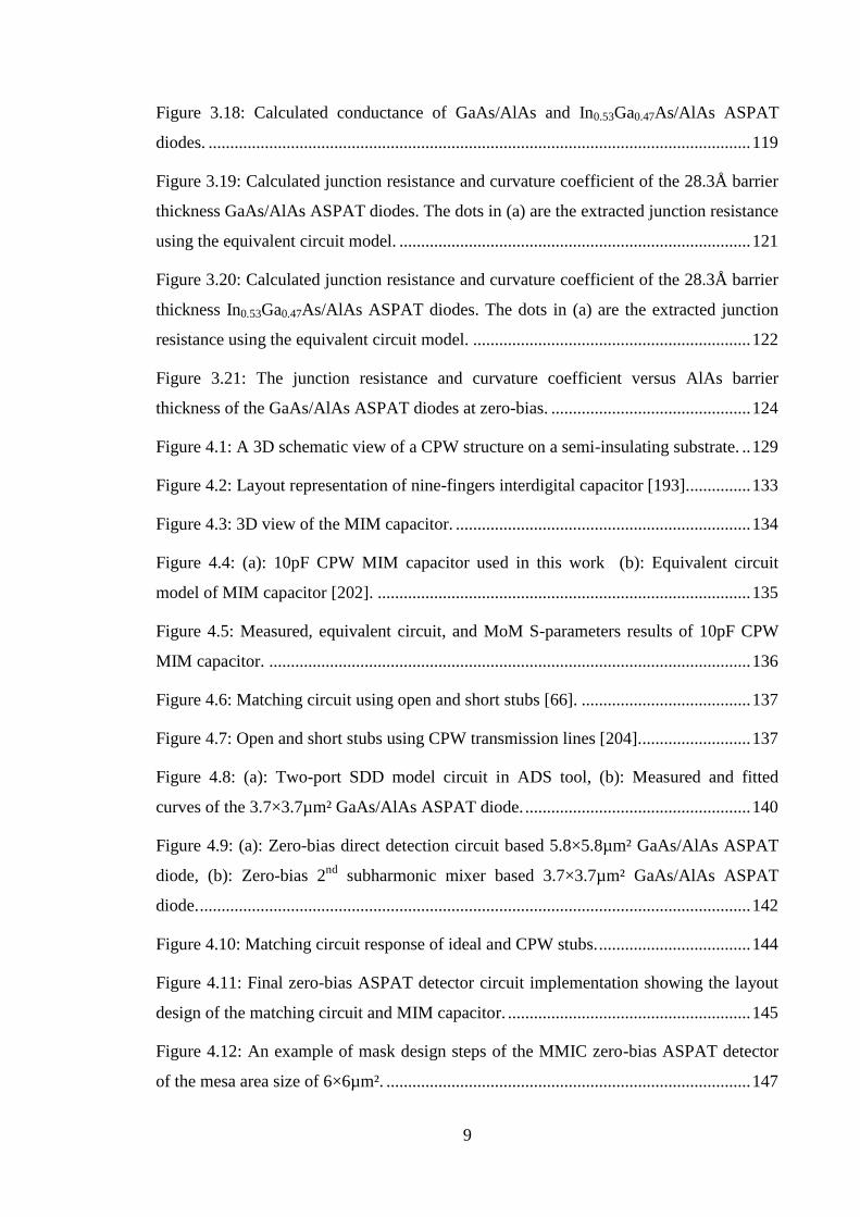
LIST OF FIGURES ............................................................................................................ 6
LIST OF SYMBOLS AND ABBREVIATIONS ............................................................. 13
ABSTRACT ...................................................................................................................... 18
DECLARATION .............................................................................................................. 20
COPYRIGHT STATEMENT ........................................................................................... 20
ACKNOWLEDGEMENT ................................................................................................ 21
DEDICATION .................................................................................................................. 22
Publications ....................................................................................................................... 23
Journal Publications ...................................................................................................... 23
Conference Publications ................................................................................................ 23
Oral and Posters Presentations ...................................................................................... 24
Awards .......................................................................................................................... 25
CHAPTER 1 : INTRODUCTION .................................................................................... 26
1.1 Introduction and Motivation .......................................................................... 26
1.2 Millimetre-Wave Applications....................................................................... 29
1.3 Millimetre-Wave Detection Techniques ........................................................ 32
1.4 Material Systems ............................................................................................ 33
1.5 Optoelectronics Approach .............................................................................. 37
1.6 Integration of Fibre-Wireless Network Systems ............................................ 38
1.7 Contribution and Thesis Outline .................................................................... 40
CHAPTER 2 : BACKGROUND AND THEORY OF DETECTION SYSTEMS........... 43
2.1 Introduction .................................................................................................... 43
2.2 Signal Sources ................................................................................................ 43
2.3 Frequency Mixer ............................................................................................ 44
2.4 Mixer Characteristics ..................................................................................... 47
2.4.1 Conversion Loss (CL) ............................................................................... 47
2.4.2 1-dB Compression ..................................................................................... 47
2.4.3 Third Order Intercept Point ....................................................................... 48
2.4.4 Isolation ..................................................................................................... 50
2.4.5 Return Loss ................................................................................................ 50
2.5 Mixer Configurations ..................................................................................... 51

2
2.6 2nd
Subharmonic Mixer .................................................................................. 53
2.7 Frequency Detector ........................................................................................ 55
2.8 Basics of Detection ........................................................................................ 56
2.9 Detector Characteristics ................................................................................. 57
2.9.1 Voltage Sensitivity .................................................................................... 57
2.9.2 Noise Equivalent Power ............................................................................ 58
2.9.3 Tangential Sensitivity and Dynamic Range .............................................. 59
2.10 Theory of Tunnel Diodes ............................................................................... 60
2.11 Tunnel Diodes ................................................................................................ 62
2.11.1 Esaki Tunnel diode .................................................................................... 63
2.11.2 Resonant Tunnelling Diode ....................................................................... 64
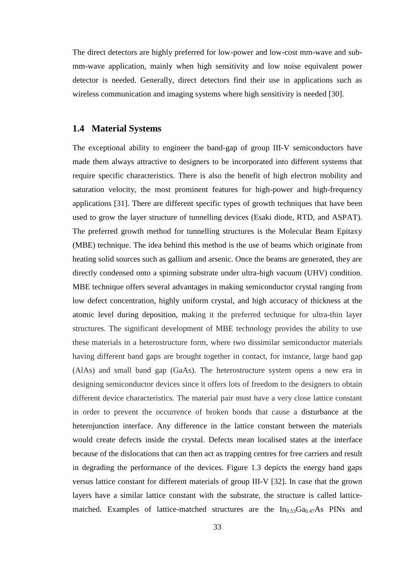
2.12 Asymmetric Spacer Layer Tunnel Diode ....................................................... 66
2.13 Operating Principle of ASPAT Diodes .......................................................... 68
2.14 Current Density of ASPAT Diode ................................................................. 69
2.15 Introduction and Overview of APD and PIN Photodetectors ........................ 71
2.16 Operational Principle of PIN Photodiode ...................................................... 73
2.17 Operational Principle of Avalanche Photodiode ............................................ 74
2.18 Photodetector Characteristics ......................................................................... 77
2.18.1 Quantum Efficiency and Responsivity ...................................................... 77
2.18.2 Dark Current .............................................................................................. 79
2.18.3 3-dB Bandwidth ........................................................................................ 81
2.18.4 Internal Gain .............................................................................................. 82
2.18.5 Punch-Through and Breakdown Voltages ................................................ 83
2.18.6 Noise characteristics .................................................................................. 85
2.19 Requirements of Multiplication and Charge Layers ...................................... 87
2.20 Summary ........................................................................................................ 88
CHAPTER 3 : FABRICATION AND CHARACTERISATION OF ASPAT DIODES . 89
3.1 Introduction .................................................................................................... 89
3.2 Epi-layer Structure of GaAs/AlAs ASPAT Diode ......................................... 89
3.3 Mask Design and Fabrication of Discrete ASPAT Diodes ............................ 90
3.4 Mask Structures .............................................................................................. 93
3.4.1 Open, Short, and ASPAT Diode Structures .............................................. 93
3.4.2 Transmission Line Model Structure .......................................................... 94
3.5 Intrinsic Parameters of ASPAT Diode ........................................................... 98

3
3.5.1 Junction Capacitance and Junction Resistance ......................................... 98
3.5.2 Series Resistance ....................................................................................... 99
3.6 DC Characteristics of GaAs/AlAs ASPAT Diodes ..................................... 101
3.7 RF Characteristics of GaAs/AlAs ASPAT Diodes ...................................... 104
3.7.1 RF Characteristics of the Open and Short Bond Pad Structures ............. 105
3.7.2 RF Characteristics of GaAs/AlAs ASPAT Diodes ................................. 111
3.8 InGaAs/AlAs ASPAT Diodes ...................................................................... 117
3.9 Extracted Junction Resistance and Curvature Coefficient of ASPAT Diodes
...................................................................................................................... 120
3.10 Summary ...................................................................................................... 125
CHAPTER 4 : DESIGN, SIMULATION AND FABRICATION OF COPLANAR
WAVEGUIDE ZERO-BIAS ASYMMETRICAL SPACER LAYER TUNNEL DIODE
DETECTORS AND MIXERS ........................................................................................ 126
4.1 Introduction .................................................................................................. 126
4.2 Electromagnetic Simulation Tools ............................................................... 127
4.3 Coplanar Waveguide Structure .................................................................... 129
4.4 Characteristic Impedance and Attenuation of CPW Structure ..................... 130
4.4.1 Conductor Loss ........................................................................................ 131
4.4.2 Dielectric and Radiation Losses .............................................................. 131
4.5 MMIC Metal-Insulator-Metal Capacitor...................................................... 133
4.6 Matching Networks ...................................................................................... 136
4.7 Modelling of ASPAT I-V Characteristics .................................................... 139
4.8 Schematic Design and Simulation of Detectors and Mixers using ADS Tool ..
...................................................................................................................... 141
4.9 Mask Layout of the MMIC Integrated Zero-Bias ASPAT Detectors .......... 143
4.10 Fabrication and Measurement of the MMIC Integrated Zero-Bias ASPAT
Detectors .................................................................................................................. 147
4.11 Measured and Simulated Un-matched Voltage Sensitivity of 6×6µm²
GaAs/AlAs ASPAT Diode ...................................................................................... 151
4.12 ASPAT Detectors Performances .................................................................. 153
4.12.1 Measured DC Output Voltage ................................................................. 153
4.12.2 Voltage Sensitivity and Noise Equivalent Power .................................... 155
4.13 Millimeter-Wave ASPAT Detectors with Antennas .................................... 158
4.14 Antenna Design and Performances Evaluation ............................................ 159
4.15 Overview of Devices Used in Detectors ...................................................... 164
4.16 2nd
Subharmonic ASPAT Mixers Performances .......................................... 169

4
4.17 Overview of the Reported Subharmonic Mixers ......................................... 172
4.18 Summary ...................................................................................................... 175
CHAPTER 5 : PHYSICAL MODELLING AND EXPERIMENTAL
CHARACTERISATION OF APD AND PIN PHOTODETECTORS FOR HIGH DATA
RATE APPLICATIONS ................................................................................................. 176
5.1 Introduction .................................................................................................. 176
5.2 Epi-layer Structures of Photodetectors......................................................... 177
5.3 Fabrication and Small Signal RF Equivalent Circuit Extraction ................. 178
5.4 Experimental Characterisation Tools ........................................................... 182
5.5 Physical Modelling Characterisation Tool ................................................... 183
5.6 Physical Modelling and Optimisation Details ............................................. 185
5.7 Dark Currents and C-V Characteristics........................................................ 188
5.8 Optical and Noise Characteristics ................................................................ 194
5.9 Reported PIN Photodetectors ....................................................................... 201
5.10 Reported APDs ............................................................................................ 204
5.11 Summary ...................................................................................................... 210
CHAPTER 6 : CONCLUSION AND FUTURE WORKS ............................................. 211
6.1 Conclusion ................................................................................................... 211
6.1.1 Zero-Bias ASPAT Detectors and Mixers ................................................ 211
6.1.2 High-Data-Rate APD and PIN Photodetectors. ...................................... 215
6.2 Suggested Ideas for Future Work ................................................................. 216
6.2.1 Millimetre-Wave Detection Circuits ....................................................... 216
6.2.2 Fabrication of the Optimised APD and PIN Photodetectors ................... 220
APPENDICES ................................................................................................................ 221
APPENDIX-A: QFN Circuit ....................................................................................... 221
APPENDIX-B: Lab View programme ........................................................................ 222
APPENDIX-C: Test Structure Used in the Mask ....................................................... 222
APPENDIX-D: Measured and Simulated 𝑆11 of the Fabricated 30GHz ASPAT
Detector with Open Stub Matching Network .............................................................. 223
REFERENCES ............................................................................................................... 224

5
LIST OF TABLES
TABLE 1. 1: A SUMMARY OF FREQUENCY BANDS CATEGORISED BY IEEE
ORGANISATION [17] ..................................................................................................... 29
TABLE 1. 2: LATTICE CONSTANT, BANDGAP, ELECTRON EFFECTIVE MASS
AND FREE-DOPING ELECTRON MOBILITY OF STANDARD BINARY AND
TERNARY COMPOUND SEMICONDUCTOR MATERIALS USED TO REALISE
PIN, APD AND TUNNEL DIODES AT 300K. ............................................................... 36
TABLE 3. 1: EPITAXIAL LAYER STRUCTURE OF ASPAT SAMPLE XMBE#304 90
TABLE 3. 2: CALCULATED SERIES RESISTANCE OF THE GaAs/AlAs ASPAT
DIODES .......................................................................................................................... 100
TABLE 3. 3: EXTRACTED INTRINSIC AND EXTRINSIC PARAMETERS OF
GaAs/AlAs ASPAT DIODES ......................................................................................... 114
TABLE 3. 4: EPITAXIAL LAYER STRUCTURE OF ASPAT SAMPLE XMBE#326
......................................................................................................................................... 117
TABLE 3. 5: EXTRACTED PARAMETERS OF THE In0.53Ga0.47As/AlAs ASPAT
DIODES AT ZERO-BIAS. ............................................................................................. 120
TABLE 4. 1: REPORTED DIRECT DETECTORS ...................................................... 167
TABLE 4. 2: SOME OF THE REPORTED 2nd
SUBHARMONIC MIXERS AND
ASPAT MIXERS PERFORMANCES ........................................................................... 174
TABLE 5. 1: EPI-LAYER STRUCTURE OF THE STANDARD In0.53Ga0.47As PIN
DIODE ............................................................................................................................ 177
TABLE 5. 2: EPI-LAYER STRUCTURE OF THE STANDARD
In0.53Ga0.47As/In0.52Al0.48As APD (30A) ......................................................................... 178
TABLE 5. 3: STANDARD APD AND PIN DIODES EXTRACTED PARAMETERS
AT FULLY DEPLETED BIAS. ..................................................................................... 181
TABLE 5. 4: THE STANDARD AND OPTIMISED DEVICES .................................. 187

6
TABLE 5. 5: KEY FITTING PARAMETERS USED IN SILVACO PHYSICAL
MODELLING. ................................................................................................................ 189
TABLE 5. 6: NOISE CHARACTERISTICS OF THE STANDARD AND OPTIMISED
APDS AND PIN DIODES AT 90%𝑉𝐵𝑅 BIAS ............................................................... 198
TABLE 5. 7: KEY REPORTED PIN PHOTODETECTOR PERFORMANCES ......... 203
TABLE 5. 8: REPORTED APD PERFORMANCES .................................................... 207
LIST OF FIGURES
Figure 1.1: mm-wave attenuation caused by atmospheric gases, rain and fog [18]. The
upper inset shows the promising applications of mm-wave systems. .............................. 30
Figure 1.2: Block diagram of (a): Heterodyne detection system, and (b): Direct detection
with amplifier [24]. ........................................................................................................... 32
Figure 1.3: Energy band gap versus lattice constant for group III-V and II-VI compound
semiconductor material systems (solid line is direct, and the dashed line is indirect) at
room temperature [32]. ..................................................................................................... 34
Figure 1.4: Block diagram of a fibre-wireless system [58]. ............................................. 39
Figure 2.1: An ideal mixer representation with two input signals (RF and LO). .............. 44
Figure 2.2: Sketch of the output frequency spectrum of a non-ideal mixer, where it is
assumed that RF power is lower than LO power [66]. ..................................................... 46
Figure 2.3: 1-dB compression point of a non-ideal mixer [72]. ....................................... 48
Figure 2.4: Basic representation of the third-order intercept point of a non-ideal mixer
[72]. ................................................................................................................................... 49
Figure 2.5: Single element unbalanced mixer showing LO and RF signals applied to the
same terminal side [66]. .................................................................................................... 52
Figure 2.6: A schematic diagram of a balanced passive mixer using two diodes and
hybrid [66]. ....................................................................................................................... 53
Figure 2.7: 2nd
sub-harmonic mixer architecture using anti-parallel diodes with open and
short stubs [85, 86]. ........................................................................................................... 54

7
Figure 2.8: Basic Detector circuit. The inset is the non-linear I-V characteristics of a
diode. ................................................................................................................................. 56
Figure 2.9: Output voltage versus RF input power showing the dynamic range of a
Schottky diode detector [101]. .......................................................................................... 60
Figure 2.10: Schematic of the incident, reflected and transmitted wave functions through
a rectangular potential barrier [104].................................................................................. 61
Figure 2.11: Schematic band diagram of the In0.8Ga0.2As/AlAs DBQWRTD. The AlAs
energy band gap is the direct gap value [113]. ................................................................. 64
Figure 2.12: Temperature dependency of (a): GaAs/AlAs and (b): In0.53Ga0.47As/AlAs
ASPAT diodes [15, 16]. .................................................................................................... 67
Figure 2.13: Schematic conduction band profile of ASPAT structure under negative, zero
and positive bias [125, 126]. ............................................................................................. 69
Figure 2.14: Operational principle of a reversed biased PIN photodetector, adapted from
[142]. ................................................................................................................................. 73
Figure 2.15: Operation of a SACM APD, (a): 2-D structure, (b): Band diagram [55, 146].
........................................................................................................................................... 76
Figure 2.16: Absorption coefficients versus light wavelength of different materials [154].
........................................................................................................................................... 78
Figure 2.17: APD excess noise factor as a function of multiplication gain (𝑀) based on
local mode theory [145]. ................................................................................................... 86
Figure 3.1: 3D structure drawing of GaAs/AlAs (XMBE#304) ASPAT diode with its
standard CPW bond pad. The inset shows the separation distance (𝐷𝑠𝑝𝑟) between the top
anode contact and bottom contact pad (cathode). ............................................................. 93
Figure 3.2: A 3D schematic and side view of the TLM structure used in the masks. (Note
that the image is not to scale). ........................................................................................... 95
Figure 3.3: Total resistance versus separated distance (𝑑𝑛) of TLM structure. [177]. ..... 96
Figure 3.4: Measured TLM of the top contact of GaAs/AlAs ASPAT XMBE#304
sample. .............................................................................................................................. 97

8
Figure 3.5: The right side is the 2D sectional view of the ASPAT diode. The left side is
the intrinsic component of each layer. .............................................................................. 98
Figure 3.6: Measured I-V characteristics of GaAs/AlAs ASPAT (wafer XMBE#304)
diodes of (a): 3.7x3.7µm2, (b): 5.8x5.8µm
2, (c): 10x10µm
2. (d): Log representation of the
measured currents showing the non-linear characteristics at zero-bias. ......................... 102
Figure 3.7: Measured current densities of the fabricated 3.7×3.7µm2, 5.8×5.8µm
2, and
10×10µm2 GaAs/AlAs ASPAT diodes using wafer XMBE#304. ................................. 103
Figure 3.8: Measured current densities of the devices from two wafers (XMBE#304 and
XMBE#421). ................................................................................................................... 104
Figure 3.9: Example of the fabricated standard CPW ASPAT diode, open, and short
structures of mesa area size 3.7×3.7µm². ........................................................................ 105
Figure 3.10: (a), (b), (c), and (d) are the real and imaginary part of 𝑆11of open and short
bond pad structures. (e) The Smith chart representation and the built circuits of the open
and short bond structures in ADS. .................................................................................. 107
Figure 3.11: The measured and simulated parasitic capacitance versus frequency of the
standard CPW structure for different substrate thicknesses. ........................................... 108
Figure 3.12: Fabricated optimised one and two-port open bond pad CPW structure. .... 109
Figure 3.13: The measured and simulated parasitic capacitance versus frequency of the
optimised CPW structure for different substrate thicknesses. ......................................... 110
Figure 3.14: (a): ASPAT equivalent circuit built in ADS at negative bias, and (b): The
measured and simulated real and imaginary parts of 𝑆11of the one-port CPW GaAs/AlAs
ASPAT diode of mesa area 3.7×3.7µm2 at -0.5V bias. .................................................. 112
Figure 3.15: (a): ASPAT equivalent circuit built in ADS at zero and forward bias, and
(b): The measured and simulated real and imaginary parts of 𝑆11of the one-port CPW
GaAs/AlAs ASPAT diode of the mesa area 3.7×3.7µm2 at zero-bias. ........................... 113
Figure 3.16: Smith chart representation of the two-port 2.4×2.4µm² ASPAT diode at
zero-bias. Red and blue lines are measured and simulated 𝑆11 respectively. Red and blue
dashed lines are the measured and simulated 𝑆12 respectively. ...................................... 116
Figure 3.17: Measured current density of the fabricated In0.53Ga0.47As/AlAs ASPAT
diodes. ............................................................................................................................. 118
9
Figure 3.18: Calculated conductance of GaAs/AlAs and In0.53Ga0.47As/AlAs ASPAT
diodes. ............................................................................................................................. 119
Figure 3.19: Calculated junction resistance and curvature coefficient of the 28.3Å barrier
thickness GaAs/AlAs ASPAT diodes. The dots in (a) are the extracted junction resistance
using the equivalent circuit model. ................................................................................. 121
Figure 3.20: Calculated junction resistance and curvature coefficient of the 28.3Å barrier
thickness In0.53Ga0.47As/AlAs ASPAT diodes. The dots in (a) are the extracted junction
resistance using the equivalent circuit model. ................................................................ 122
Figure 3.21: The junction resistance and curvature coefficient versus AlAs barrier
thickness of the GaAs/AlAs ASPAT diodes at zero-bias. .............................................. 124
Figure 4.1: A 3D schematic view of a CPW structure on a semi-insulating substrate. .. 129
Figure 4.2: Layout representation of nine-fingers interdigital capacitor [193]. .............. 133
Figure 4.3: 3D view of the MIM capacitor. .................................................................... 134
Figure 4.4: (a): 10pF CPW MIM capacitor used in this work (b): Equivalent circuit
model of MIM capacitor [202]. ...................................................................................... 135
Figure 4.5: Measured, equivalent circuit, and MoM S-parameters results of 10pF CPW
MIM capacitor. ............................................................................................................... 136
Figure 4.6: Matching circuit using open and short stubs [66]. ....................................... 137
Figure 4.7: Open and short stubs using CPW transmission lines [204]. ......................... 137
Figure 4.8: (a): Two-port SDD model circuit in ADS tool, (b): Measured and fitted
curves of the 3.7×3.7µm² GaAs/AlAs ASPAT diode. .................................................... 140
Figure 4.9: (a): Zero-bias direct detection circuit based 5.8×5.8µm² GaAs/AlAs ASPAT
diode, (b): Zero-bias 2nd
subharmonic mixer based 3.7×3.7µm² GaAs/AlAs ASPAT
diode. ............................................................................................................................... 142
Figure 4.10: Matching circuit response of ideal and CPW stubs. ................................... 144
Figure 4.11: Final zero-bias ASPAT detector circuit implementation showing the layout
design of the matching circuit and MIM capacitor. ........................................................ 145
Figure 4.12: An example of mask design steps of the MMIC zero-bias ASPAT detector
of the mesa area size of 6×6µm². .................................................................................... 147

10
Figure 4.13: Fabricated MMIC integrated zero-bias ASPAT detectors. (a) and (b) are the
X-band detectors, (c) and (d) are the K-band detectors (Note: the images are not to
scale). .............................................................................................................................. 150
Figure 4.14: Circuit diagram for voltage sensitivity measurement configuration. ......... 150
Figure 4.15: (a) Equivalent circuit diagram of the QFN detector, (b) Actual photograph
of discrete circuit. ............................................................................................................ 151
Figure 4.16: Measured and simulated un-matched voltage sensitivity of 6×6µm² ASPAT
diode. The inset is the measured video resistance. ......................................................... 152
Figure 4.17: (a), (b), and (c) are the measured output DC voltage and reflection
coefficients (𝑆11) of the X-band zero-bias detectors based 5.8×5.8µm² and 10×10µm²
GaAs/AlAs ASPAT diodes at -27dBm RF power. (d), (e), and (f) are the measured
output DC voltage and reflection coefficients (𝑆11) of the K-band zero-bias detectors
based 3.7×3.7µm² and 5.8×5.8µm² GaAs/AlAs ASPAT diodes at -27dBm RF power. 154
Figure 4.18: (a) and (b) are the measured and simulated voltage sensitivity and calculated
noise equivalent power of the X-band and K-band zero-bias detectors based 5.8×5.8µm²
ASPAT diode, (c) is the measured and simulated voltage sensitivity versus input RF
power. .............................................................................................................................. 156
Figure 4.19: A 3D structure of the proposed ASPAT detector with a bow-tie antenna.
(Note: image is not to scale). .......................................................................................... 159
Figure 4.20: Top view of the proposed 250GHz bow-tie antenna with (a): Coplanar strip
output pads, and (b): Coplanar waveguide output pads. ................................................. 161
Figure 4.21: Simulated return loss (𝑆11) of the proposed 77GHz and 250GHz bow-tie
antennas on a 100µm GaAs substrate. ............................................................................ 161
Figure 4.22: Simulated radiation patterns (gain) of the proposed 250GHz bow-tie antenna
on a 100µm GaAs substrate. ........................................................................................... 162
Figure 4.23: Simulated voltage sensitivity of the zero-bias ASPAT detectors with bow-tie
antennas at 77GHz and 250GHz. .................................................................................... 163
Figure 4.24: Simulated conversion loss of the 3.7×3.7µm² GaAs/AlAs and 3.75×3.75µm²
In0.53Ga0.47As/AlAs 2nd
subharmonic mixers at 77GHz RF signal. ................................ 169

11
Figure 4.25: 1-dB compression of the 3.7×3.7µm² GaAs/AlAs and 3.75×3.75µm²
In0.53Ga0.47As/AlAs 2nd
subharmonic mixers at 77GHz RF signal. ................................ 170
Figure 4.26: (a): Spectrum of the IF Current in dB, (b): 3rd
intercept points of the
3.7×3.7µm² GaAs/AlAs subharmonic mixers at 77GHz RF signal. ............................... 171
Figure 5.1: Fabricated photodetector. The inset shows the light window aperture (W) and
𝐷𝑔𝑎𝑝 of the photodetector. (images are not to scale). .................................................... 179
Figure 5.2: Measured and simulated 𝑆11 represented on smith charts of the open and short
structures and corresponding equivalent circuits. ........................................................... 180
Figure 5.3: Measured and simulated S-parameters represented on Smith charts and of the
standard PINs and APD at fully depleted bias. ............................................................... 180
Figure 5.4: Optical system set up on-wafer measurements. ........................................... 182
Figure 5.5: Modelled 3D rectangular photodetector. ...................................................... 185
Figure 5.6: Calculated 3-dB optical bandwidth of the optimised In0.53Ga0.47As/
In0.52Al0.48As APD. ......................................................................................................... 187
Figure 5.7: Measured and simulated dark currents of the standard and optimised
(a): In0.53Ga0.47As/In0.52Al0.48As APDs, and (b): In0.53Ga0.47As PIN photodetectors. ..... 191
Figure 5.8: Measured and simulated dark junction capacitance versus bias of the standard
and optimised (a): In0.53Ga0.47As/In0.52Al0.48As APDs, and (b): In0.53Ga0.47As PIN
photodetectors. ................................................................................................................ 193
Figure 5.9: Simulated electric field distribution of the In0.53Ga0.47As/In0.52Al0.48As
standard and optimised APDs under -20V bias. ............................................................. 195
Figure 5.10: Measured and simulated photocurrents of the standard and optimised (a):
In0.53Ga0.47As/In0.52Al0.48As APDs, and (b): In0.53Ga0.47As PIN diodes. ......................... 196
Figure 5.11: Measured and simulated internal gain and excess noise factor of the standard
and optimised In0.53Ga0.47As/In0.52Al0.48As APDs. ......................................................... 197
Figure 5.12: Normalized 𝑆21 response of the In0.53Ga0.47As/In0.52Al0.48As APD and
In0.53Ga0.47As PIN diode, (red and black are the measured and simulated standard APD
(30A), blue is the simulated optimised APD (15A), green and brown lines refer to the
measured and simulated standard PIN diode (15S), and purple is the simulated optimised
PIN diode (15D)). ........................................................................................................... 199

12
Figure 5.13: Measured and simulated 3-dB Bandwidth versus bias of the standard and
optimised In0.53Ga0.47As/In0.52Al0.48As APDs. ............................................................... 200
Figure 6.1: Flow chart of the future work of the zero-bias ASPAT detector for mm-wave
and sub-mm-wave applications. ...................................................................................... 217

13
LIST OF SYMBOLS AND ABBREVIATIONS
µ𝑛 Electron Mobility
ℎ𝑐 Critical Thickness
Ɍ𝐴𝑃𝐷 The responsivity of APD
Ɍ𝑃−𝐼−𝑁 The responsivity of PIN photodetector
Zsource The impedance of the source
𝐶𝐽 Junction Capacitance
𝐶𝑃 Parasitic Capacitance
𝐶𝑑 Displacement Capacitor
𝐷𝑠𝑝𝑟 The separation between anode and cathode
𝐹3𝑑𝐵 3-dB Bandwidth
𝐼𝑑𝑖𝑓𝑓 The diffusion current
𝐼𝑔−𝑟 The generation-recombination current
𝐾𝑉 Curvature Coefficient
𝐿𝑃 Parasitic Inductance
𝑅𝐽 Junction Resistance
𝑅𝑆 Series Resistance
𝑅𝑉 Video Resistance
𝑅𝑐 Contact Resistance
𝑅𝑠ℎ Sheet Resistance
𝑅𝑢 Non-linear resistance of the un-depleted layers
𝑆𝑉 Voltage Sensitivity
𝑉0 Barrier Height
𝑉𝐵𝑅 The breakdown voltage
𝑉𝑃𝑇 The punch-through voltage
𝑉𝑠𝑎𝑡𝑛 Saturation velocity for electrons
𝑍𝑙𝑜𝑎𝑑 The impedance of the load
𝑎𝐿 The lattice constant of the grown layer

14
𝑎𝑆 The lattice constant of the substrate
𝑓𝑐𝑢𝑡−𝑜𝑓𝑓 Cut-off frequency
𝑔𝑚 Trans-Conductance
𝑘𝑟𝑎𝑡𝑖𝑜 The ratio between the hole and electron impact ionisation
𝑙𝑒𝑥𝑡 Parasitic Extension Length
𝑚∗ Effective mass
𝛼𝑑 Dielectric Loss
𝛼𝑟 Radiation Loss
휀𝑠 Built-in strain
𝜌𝑚 The temperature coefficient of breakdown voltage
1/𝑓 Corner Frequency
2D Two Dimensional
3D Three Dimensional
5G Fifth Generation
A/Amp Ampere (Current Unit)
AC Alternating Current
ADS Advanced Design System
AlAs Aluminium Arsenide
AlGaAs Aluminium Gallium Arsenide
AlSb Aluminium Antimonide
APD Avalanche Photodiode
AR Anti-Reflection
ASPAT Asymmetric Spacer Tunnel Layer Diode
BER Bit Error Rate
BJT Bipolar Junction Transistor
CPW Coplanar Waveguide
C-V Capacitance-Voltage
CW Continuous Wave
DBQW Double-Barrier Quantum Well
DC Direct Current

15
DI De-Ionised
DUT Device under Test
EBL Electron Beam Lithography
EC Conduction Band
EM Electromagnetic
eV Electron Volt
EV Valence Band
FEM Finite Element Method
FIT Finite Integration Technique
FLDMOB Field Mobility model
FTTH Fibre-to-the-Home
GaAs Gallium Arsenide
GBP Gain Bandwidth Product
Ge Germanium
GEC General Electrical Company
GHz Gigahertz
GSG Ground-Signal-Ground
HB Harmonic Balance
HBT Heterojunction Bipolar Transistor
HEMT High Electron Mobility Transistor
IC Integrated Circuit
IF Intermediate Frequency
InAlGaAs Indium Aluminium Gallium Arsenide
InAs Indium Arsenide
InGaAs Indium Gallium Arsenide
InP Indium Phosphide
IoT Internet of Things
IP3 Third Order Intercept Point
I-V Current Voltage
K Kelvin

16
LCA Lightwave Component Analyser
LNA Low Noise Amplifier
LO Local Oscillator
M Multiplication Factor (internal gain)
MBE Molecular Beam Epitaxy
MIC Microwave Integrated Circuit
MIM Metal-Insulator-Metal
ML Mono Layer
mm Millimetre
MMIC Monolithic Microwave Integrated Circuit
MOCVD Metal Organic Chemical Vapour Deposition
MoM Momentum of Method
MOVPE Molecular Organic Vapour Phase Epitaxy
MSM Metal-Semiconductor-Metal
ƞ Quantum efficiency
NDR Negative Differential Resistance
NEP Noise Equivalent Power
NiCr Nickel Chromium
nm Nanometre
pF Pico Farad
PON Passive Optical Network
PVCR Peak to Valley Current Ratio
QCL Quantum Cascade Lasers
R_Collector The resistance of the Collector layer
R_Emitter The resistance of the Emitter Layer
R_spreading (𝑅𝑠𝑝𝑟) Spreading Resistance
R_top ohmic The resistance of the top Ohmic layer
RC Resistance and Capacitance
RF Radio Frequency
RHS Right Hand Spinner

17
RTD Resonant Tunnelling Diode
SACM Separated Absorption, Charge, and Multiplication APD
SAM Separated Absorption and Multiplication APD
SDD Symbolically Defined Device model
SHM Subharmonic Mixer
Si Silicon
SIS Semiconductor-Insulator-Semiconductor
SNR Signal to Noise Ratio
SRH Shockley-Read-Hall
SSMBE Solid Source Molecular Beam Epitaxy
TBRTD Triple Barrier Resonant Tunnelling Diode
THz Terahertz
TIA Trans-impedance Amplifier
TL Transmission Line
TLM Transmission Line Model
TLMx Transmission Line Matrix
TSS Tangential Sensitivity
UHV Ultra-High Vacuum
V Volt (Voltage Unit)
VNA Vector Network Analyser
δ Skin Depth of the film
Г Reflection Coefficient
𝐶𝐿 Conversion Loss
𝐹(𝑀) The Excess noise factor
𝐺 Conductance Loss
𝑅𝐿 Return Loss
𝛼(𝐸) Impact Ionisation Rate For the Electron
𝛽(𝐸) Impact Ionisation Rate For the Hole
𝜌 Resistivity

18
ABSTRACT
The work in this thesis was concerned with the analysis, modelling, design, testing and
improvement of detectors using InP and GaAs-based technologies for electronic and
optical receiver systems.
For the electronic receivers, two types of Asymmetric Spacer Tunnel (ASPAT) diodes
were studied and tested for potential microwave and mm-wave applications including
novel X-band and K-band zero-bias tunnel diode frequency detectors. The core element
of the detectors is a GaAs/AlAs ASPAT diode. DC and high-frequency S-parameter
characterisation of diodes of mesa sizes of 1.6×1.6µm², 2.4×2.4µm², 3.7×3.7µm²,
5.8×5.8µm² and 10×10µm² were carried out to fully extract their extrinsic and intrinsic
components for optimum detector and 2nd
subharmonic mixer circuits analysis and
design. Coplanar waveguide matching circuit structures were designed and optimised to
minimise the mismatch between the RF source and the diode impedance. The detectors
were fabricated and experimentally measured in the frequency bands (4 to 18) GHz and
(10 to 35) GHz at various input powers. The maximum measured sensitivity is 3650V/W
and 1300V/W at 11GHz and 24GHz respectively for -27dBm incident RF power. The
minimum calculated noise equivalent power is (~6pW/√𝐻𝑧) and (~20pW/√𝐻𝑧) for the
X-band and K-band detectors, respectively. The 1.6×1.6µm² ASPAT offered a maximum
sensitivity of (1850V/W) at 250GHz.
The ASPAT diodes were then used in a simulation work to test and examine their
performance in mm-wave heterodyne circuits. At 77GHz RF signal, a moderate
conversion loss of 10dB was achieved using the 3.7×3.7µm² GaAs/AlAs, while a 16dB
was obtained using the 3.75×3.75µm² In0.53Ga0.47As/AlAs ASPAT diodes at 0dBm LO
power. These detectors show excellent performances, comparable to reported X-band and
K-band detectors based Schottky diodes but with the added advantage of stable operation
over a wide temperature range. The results reported here validate the models developed
which can be used to realise low cost, extremely low power, temperature-insensitive
high-frequency tunnel diode detectors for a range of applications.
The second part of the thesis dealt with telecommunication optoelectronic receivers.
Validated SILVACO physical models were exploited to optimise the electrical and
optical characteristics of 1.55µm wavelength In0.53Ga0.47As/In0.52Al0.48As avalanche
photodiodes (APD) and In0.53Ga0.47As PIN diodes. Optimised SILVACO models were

19
created by selectively thinning down the absorption layers to further reduce the carrier
transit time. Further optimisation was accomplished through scaling of the light window
aperture and mesa area sizes to reduce the device capacitances. The optimised PIN diode
provides a maximum optoelectric bandwidth of (35GHz) with a current responsivity of
(0.4A/W) under -5V bias and (10µW) incident optical power. At 1µW incident optical
power, the maximum optoelectric bandwidth and current responsivity of the optimised
avalanche diode are (21GHz) and (1.4A/W) under -21.5V bias. The optimised avalanche
and PIN photodetectors are capable of working at a data rate of up to 25Gb/s and 40Gb/s
respectively.

20
DECLARATION
No portion of the work referred to in the thesis has been submitted in support of an
application for another degree or qualification of this or any other university or other
institutes of learning.
COPYRIGHT STATEMENT
i. The author of this thesis (including any appendices to this thesis) owns certain
copyright or related rights in it (the “Copyright”), and he has given The
University of Manchester certain rights to use such Copyright, including for
administrative purposes.
ii. Copies of this thesis, either in full or in extracts and whether in hard or electronic
copy, may be made only in accordance with the Copyright, Designs and Patents
Act 1988 (as amended) and regulations issued under it or, where appropriate, in
accordance with licensing agreements which the University has from time to
time. This page must form part of any such copies made.
iii. The ownership of certain Copyright, patents, designs, trademarks and other
intellectual property (the “Intellectual Property”) and any reproductions of
copyrightworks in the thesis, forexamplegraphsand tables (“Reproductions”),
which may be described in this thesis, may not be owned by the author and may
be owned by third parties. Such Intellectual Property and Reproductions cannot
and must not be made available for use without the prior written permission of the
owner(s) of the relevant Intellectual Property and/or Reproductions.
iv. Further information on the conditions under which disclosure, publication and
commercialisation of this thesis, the Copyright and any Intellectual Property
and/or Reproductions described in it may take place is available in the University
IP Policy, in any relevant Thesis restriction declarations deposited in the
UniversityLibrary,TheUniversityLibrary’sregulationsandinTheUniversity’s
policy on Presentation of Theses.

21
ACKNOWLEDGEMENT
I would like to express my great appreciation to my supervisor, Professor Mohamed
Missous, who offered me this valuable opportunity to do research at the University of
Manchester and for his highly professional character in the process of consultation and
guidance that continuously improved my knowledge during the PhD study. Also special
thanks to my fellow colleagues for their cooperation towards understanding the ideas in
this study.
At the same time, I would like to show my gratefulness to my parents, especially my
father who passed away at the time of submission (May the God (Allah) forgive him and
accept his good deeds). My parents have encouraged me along with my life; I dedicate a
special and heartiest tribute to them for their help and support.
Finally, my special thanks to the Higher Committee for Education Development in Iraq
(HCED) for giving me the opportunity to conduct this PhD research and for their
financial support, without them this PhD would not have been started.

22
DEDICATION
This thesis is dedicated to my parents, who always supported me through
all my studies.
Omar

23
PUBLICATIONS
Journal Publications
1. O. S. Abdulwahid, I. Kostakis, S. G. Muttlak, J. Sexton, K.W. Ian and M.
Missous, “PhysicalModelling of InGaAs-InAlAs APD and PIN Photodetectors
for >25Gb/s Data Rate Applications”, IET Optoelectronics, DOI: 10.1049/iet-
opt.2018.5030.
2. O. S. Abdulwahid, J. Sexton, I. Kostakis, K. Ian, and M. Missous, "Physical
modelling and experimental characterisation of InAlAs/InGaAs avalanche
photodiode for 10 Gb/s data rates and higher," IET Optoelectronics, vol. 12, no.
1, pp. 5-10, 2017.
3. Saad G. Muttlak, O. S. Abdulwahid, J. Sexton, M.J. Kelly and M. Missous,
“InGaAs/AlAs Resonant Tunneling Diodes for THz Applications: An
ExperimentalInvestigation”,IEEEJournaloftheElectronDevicesSociety,DOI:
10.1109/JEDS.2018.2797951.
4. Muttlak SG, Kostakis I, Abdulwahid OS, Sexton J, Missous M. Low-cost InP–
InGaAs PIN–HBT-based OEIC for up to 20 Gb/s optical communication systems.
IET Optoelectronics. 2019 Jan 11;13(3):144-50.
5. K. N. Zainul Ariffin, Y. Wang, M. R. R. Abdullah, S. G. Muttlak, Omar S.
Abdulwahid, J. Sexton, Ka Wa Ian, Michael J. Kelly and M. Missous,
“Investigations ofAsymmetricSpacerTunnel Layer (ASPAT)Diode forHigh-
Frequency Application” IEEE Transaction Electron Devices,
DOI:10.1109/TED.2017.2777803.
Conference Publications
1. O. S. Abdulwahid, SaadG.Muttlak, J. Sexton,M.Missous,M. J.Kelly, “24
GHz Zero‐Bias Asymmetrical Spacer Layer Tunnel Diode Detectors”,UCMMT
2019, IEEE proceedings, August 2019.
2. Saad G. Muttlak , O. S. Abdulwahid, J. Sexton, M. Missous, M. J. Kelly,
“InGaAs/AlAs Resonant Tunnelling Diodes with Highest Negative Differential

24
Conductance for Efficient and Cost-Effective mm-wave/THz Sources”,UCMMT
2019, IEEE proceedings, August 2019.
3. Abdelmajid Salhi, James Sexton, Saad Muttlak, Omar Abdulwahid and
Mohamed Missous, “InGaAs/AlAs metamorphic Asymmetric Spacer Tunnel
(mASPAT) Diodes on GaAs substrate for Microwave/millimetre-wave
Applications”, UCMMT 2019, IEEE proceedings, August 2019.
4. O. S. Abdulwahid, Saad G. Muttlak, J. Sexton, M. Missous, K. W. Ian, M. J.
Kelly, “2nd Subharmonic mixer based asymmetric spacer tunnel diode
(ASPAT)”, UCMMT 2017, IEEE proceedings, September 2017, DOI:
10.1109/UCMMT.2017.8068352.
5. Saad G. Muttlak, O. S. Abdulwahid, J.SextonandM.Missous, “Modelingof
high gain and μW level power consumption resonant tunneling diode based
amplifiers”, UCMMT 2017, IEEE proceedings, September 2017, DOI:
10.1109/UCMMT.2017.8068351.
6. K. N. Zainul Ariffin, M. R. R. AbduUah, Y. K. Wang, Saad G. Muttlak, O. S.
Abdulwahid, J. Sexton; M. Missous andM.J.Kelly,“Asymmetricspacerlayer
tunnel diode (ASPAT), quantum structure design linked to current-voltage
characteristics:Aphysicalsimulationstudy”,UCMMT2017,IEEEproceedings,
DOI: 10.1109/UCMMT.2017.8068358.
Oral and Posters Presentations
1. O. S. Abdulwahid, Saad Muttlak, J. Sexton, K. N. Zainul Ariffin, M.J. Kelly and
M. Missous, “Modelling and Characterization of Zero-Bias Asymmetrical Spacer
Layer Tunnel Diode Detectors”, SIOE Conference 2019. Cardiff, Oral
Presentation.
2. O. S. Abdulwahid, Saad Muttlak, J. Sexton, M.J. Kelly and M. Missous, “15-35
GHz Zero-Bias Asymmetrical Spacer Layer Tunnel Diode Detectors”, UK
Semiconductor Conference 2019, Sheffield, Oral Presentation.
3. O. S. Abdulwahid, Saad Muttlak, J. Sexton, M.J. Kelly and M. Missous,
“Modelling and Characterization of Zero-Bias Asymmetrical Spacer Layer

25
Tunnel Diode Detectors”, THz Electronics Workshop 2018, Glasgow, Poster
Presentation.
4. O. S. Abdulwahid, Saad Muttlak, J. Sexton, M.J. Kelly and M. Missous, “55-80
GHz Detector based Asymmetric Spacer Tunnel Diode (ASPAT)”, UK
Semiconductor Conference 2017, Sheffield, Oral Presentation.
5. O.S. Abdulwahid, S. G. Muttlak, J. Sexton, I. Kostakis, K.W. Ian, and M.
Missous, “Physical Modelling and Experimental Characterization of High Speed
InAlAs/InGaAs Avalanche Photodiode”, Silicon photonics adoption in UK
industry 2017, Coventry, Poster Presentation.
6. Omar S. Abdulwahid, Mohd Rashid Redza Abdullah, S. G. Muttlak, K. N.
Zainul Ariffin, and Mohamed Missous, “Tunneling Barrier Diode for Millimeter
Wave Mixing”, UK Semiconductor Conference 2016, Sheffield, Oral
Presentation.
7. Omar S. Abdulwahid, S. G. Muttlak, K. N. Zainul Ariffin, M. Missous,“Next
generation Gb/s communication system: Optical and RF wireless convergence”,
EEE Poster Conference 2016, Manchester, Poster Presentation.
Awards
Best student paper shortlisting at the UCMMT2019 conference, London.
2nd
best poster presentation at Silicon photonics adoption in UK industry 2017,
Coventry

26
CHAPTER 1: INTRODUCTION
1.1 Introduction and Motivation
The perceived advantages of semiconductors have always been making them the prefered
choice for ultra-low power and high-speed electronic/optical systems for a range of
applications. The recent advances in Molecular Beam Epitaxy (MBE) technique have
paved the way for discovery of new device phenomena and growth of multi-layers
structures with atomic-level thickness resolution such as heterojunction bipolar
transistors (HBTs), avalanche breakdown (APDs) and resonant tunnelling diodes
(RTDs).
The last two decades have seen a growing trend towards designing high-frequency
communication systems that can accommodate the massive demand for high data-rate
wireless communication devices in anticipation of the Internet of Things (IoT)
applications. The high-frequency band is also highly beneficial for high-resolution
imaging applications [1]. In order to provide high-data-rate systems, the new systems
need to work at higher frequencies in both the millimetre-wave (30 to 300GHz) and sub-
millimetre-wave bands (0.3 to 3THz). The latter is also known as the terahertz (THz)
band. Besides the primary goal of improving the performance of high-frequency devices,
the ambition is to reduce the cost of these components [2]. The mm-wave/terahertz
frequencies have received much attention, and many efforts have been expanded into
making mm-wave/terahertz systems to accommodate the vast need for fast-speed links.
To date, the mm-wave and sub-mm-wave frequency bands have shown to be promising
regions for various applications such as high-resolution imaging in medical, security and
surveillance field; atmospheric monitoring and environment, radio astronomy as well as
compact range radars [3]. However, the progress of exploring room-temperature
operating mm-wave/THz electronic devices is still in early stages compared to
microwave and photonic devices. The lack of robust, powerful and room-temperature
operating mm-wave/THz sources and detectors has impeded further progress and broader
deployment of this technology leading to what is usually termed as the THz gap in the
frequency spectrum.
The most important part of a communication system is the receiver front end, which is
responsible for receiving, detecting, and processing information. Therefore, it is

27
necessary to realise a detection system that is capable of functioning efficiently in the
mm-wave/THz frequency band at both low and high ambient temperatures [2]. Systems
are constrained by the best possible integrated components (source, mixer, and detector)
to achieve their full potential [4]. These components are the core elements of the wireless
communication devices such as mobile phones and tablets.
Minimising the power consumption of such systems in the high-frequency bands is the
primary motivation for proposing different structures with different characteristics. High
power consumption reduces the running time of portable devices and also raises the
temperature of the systems. Heat dissipation techniques are usually utilised to cool down
the device temperature, yet, this is not straightforward for small size and compact THz
systems. Low-power consumption systems require zero-bias circuits to eliminate the
need for an external biasing circuit as well as reducing noise.
Detectors and mixers have been implemented using both two-terminal (diodes) and
three-terminal devices (transistors). The latter requires external bias to function as a
detector element properly, and moreover, three-terminal devices such as HEMT or HBT
transistors must be fabricated with nano-scale features (gate length and base) to reach
mm-wave operating frequency [5]. As a result, they require complicated and expensive
fabrication processes.
Research has been ongoing for many years to develop zero-bias two-terminal passive
elements for high-sensitivity detector circuits at mm-wave frequencies. At higher
frequencies, the commonly preferred diode is the metal-semiconductor Schottky diode.
This majority carrier diode has fast recovery time and increased rectification efficiency.
The barrier height in a Schottky diode controls the flow of electrons by means of
thermionic emission. Applying a positive bias across a Schottky diode decreases the
effective barrier height and leads to large current flow through the diode. The smaller
barrier height is also more effective compared to a p-n diode, resulting in the Schottky
diode having higher sensitivity for low power received RF signals [6]. However, in both
p-n and Schottky diodes, the number of electrons changes exponentially with
temperature.
The implication is that the current is very dependent upon the operating temperature. As
a result of that, detector performance based on p-n or Schottky diodes varies as the
temperature changes. A developed version of the Schottky diode was suggested with a

28
reduced effective barrier height and shifted non-linear point close to zero-bias. Improved
performances of a low-barrier InGaAs Schottky for zero-bias mm-wave detection were
reported in [7-9]. The backward tunnel diode was also demonstrated as a detector
element with its zero-bias feature. Low noise and zero-bias direct detectors fully matched
backward diodes offer a high sensitivity exceeding (10000V/W) at mm-wave frequencies
[10-12]. Nonetheless, the backward diode is still not commercially available to be
implemented in practical circuits due to the limited dynamic range, complicated epi-layer
structures and poor reproducibility.
Therefore, there is an urgent need to examine and study new zero-bias diode structures
that can overcome Schottky and backward diodes limitations and work effectively at
high-frequencies as well as being almost temperature independent. The resonant
tunnelling diode (RTD) can be used as a low-noise and room-temperature detector
exploiting its non-linear transition before the negative differential resistance (NDR)
region. The short intrinsic transit tunnelling time grants these diodes the ability to operate
at high-speed with stable switching action, well into the mm-wave/THz regime. For zero-
bias operation, a new tunnelling diode called the Asymmetrical Spacer Layer Tunnel
diode (ASPAT) developed by RT. Syme [13] and optimised by M. Missous at the
University of Manchester [14] has been further investigated and tested in this work. In-
depth discussions regarding the ASPAT diode and its principle of operation as well as its
main characteristics are reported in chapters two and three. The key feature of this diode
is its highly pronounced non-linear characteristic at zero-bias, so it is expected to behave
as an efficient zero-bias detector at high frequencies, as well as having other benefits
such as temperature insensitivity [15, 16].
The THz field also comprises the high-data-rate optoelectronic devices beyond 10Gb/s.
Fibre optic transmission has gained much attention for wide-band analogue and digital
systems, and it is expected that very shortly optical links would replace most electrical
links where very high transmission data rates are needed as is the case for Fibre-To-The-
Home (FTTH) systems. The PIN and APD diodes have been extensively investigated and
optimised for data rate up to 100Gb/s. Full-scale characterisations of the photodetectors
using available physical modelling tool before the fabricated circuits are helpful in the
prediction of prospective performances and to aid in further optimisations. This work
includes the design, characterisations and physical modelling of different PIN and APD

29
photodetectors for >10Gb/s receivers. The photodetectors are made of InGaAs absorber
to detect light at a wavelength of 1.55µm.
1.2 Millimetre-Wave Applications
The millimetre-wave band is defined as the range of frequencies between 30 to 300GHz
and correspondingly a wavelength of 10 to 1mm. The band is located between the
infrared wave and microwave bands. In general, the microwave and mm-wave
frequencies are divided into bands, as described by the IEEE and summarised in table 1.1
[17].
TABLE 1. 1: A SUMMARY OF FREQUENCY BANDS CATEGORISED BY IEEE
ORGANISATION [17]
IEEE standard
band X K Ka V W mm-wave
Frequency (GHz) 8-12 12-27 27-40 40-75 75-110 110-300
The sub-millimetre wave band corresponds to the frequencies lying beyond 300GHz and
up to 3000GHz and the wavelength correspondingly between (1 to 0.1mm). Despite the
great achievements of covering a wide range of promising applications, the development
of efficient mm-wave and sub-mm-wave systems is still in progress, and more efforts are
needed to realise reliable and high-power solid-state sources and very sensitive detectors
of low RF power signal.
The use of the mm-wave frequencies in data transmission and sensing application offers
several considerable benefits such as: firstly, high-data-rate due to the wide bandwidth of
operation, secondly, short wavelength and thus small size of antenna leading to compact
systems, thirdly, mm-waves penetrate through fog, snow and dust much better than
optical wavelength, and finally, mm-wave transceivers can be monolithically integrated,
resulting in robust, compact, and low-cost systems [18]. The mm-wave band has not yet
been extensively utilised, and still, many frequencies can be employed to mitigate the
congestion in the microwave frequencies, which can lead to improving the performance
of newly emerging (and promising) applications. So, attention is rapidly growing to
explore the mm-wave band in many civil and military applications [19]. However, the
propagation of mm-waves is limited by atmosphere attenuation rates due to the

30
absorption of gases, rain and water vapour as shown in figure 1.1 leading to dividing the
band into sections for various applications such as radar, medical, security and military,
wireless communications and others.
Figure 1.1: mm-wave attenuation caused by atmospheric gases, rain and fog [18]. The upper inset
shows the promising applications of mm-wave systems.
The low attenuation rate in the frequency bands (26 to 42GHz), (70 to 120GHz), and
(180 to 280GHz) makes them attractive options for short and long-range wireless
transmission in many applications including satellite communications, military, backhaul

31
and point to multi-point communications. In [19], a 10Gb/s wireless communication link
over a distance of 800m was successfully implemented using InP technology with an
operating frequency of 120GHz. There is an ever-increasing demand for high-data-rate
systems mainly for the upcoming 5G technology that will work in the frequency band
from (24 to 86GHz). However, It was recently stated [20] that 5G technology will
initially start deployment at 6GHz, and will then shift to mm-wave frequencies in 5
years. The non-ionised mm-wave frequencies also find use in the medical treatments of
tumours using radiation therapy that requires low intensity at frequencies such as
42.25GHz, 46.88GHz, 53.57GHz, and 61.2GHz [21, 22]. The mm-waves can penetrate
through materials such as cloths and plastic while it reflects from metals. These
properties have encouraged the use of mm-waves in the implementation of imaging
systems for security and non-destructive inspection applications [23]. Imaging systems
can be classified as either passive or active imaging. The latter uses a source to emit
waves and a detector to detect the reflected waves from objects, unlike the passive one,
which only uses a detector to sense the thermal behaviour of objects. Passive imaging
systems are less complicated and inexpensive, but they require a receiver with low-noise
and high sensitivity characteristics [24]. In imaging systems, the choice of the frequency
is mostly related to the penetration depth and spatial resolution. The low attenuation rate
at 77GHz, 94GHz, 140GHz, and 220 to 280GHz makes these regions key for high-
resolution imaging systems. A passive imaging camera for security applications designed
to work at a centre frequency of 77GHz was demonstrated in [25]. In [26], the Fujitsu
company has developed a 94GHz passive imaging sensor for security applications. The
sensor includes a HEMT transistor, low noise amplifier (LNA), and a zero-bias Schottky
detector with a voltage sensitivity of (150V/W).
Moreover, the advantages of non-ionised mm-waves can be utilised for realising imaging
systems for body scanners in airports as a potential replacement for X-ray technology.
Recently, Rohde & Schwarz introduced a fully electronic mm-wave high-resolution body
scanner which works without any moving parts in the frequency band of 70 to 80GHz
and capable of transmitting a maximum power of 1mW [27]. To date, the exploitation of
the 220 to 280GHz band is still in its infancy, and much progress remains to be made to
build and realise high-resolution imaging systems.
So far, the most appealing application from a commercial viewpoint is the automotive
radar sensor, which is usually installed behind car bumpers. The targeted frequencies

32
range is between 76 to 81GHz with a centre frequency of 77GHz where there is low
atmospheric attenuation. The high absorption of the bumper materials (plastic and paints)
presents a challenging issue in designing such sensor; therefore, the transceiver is usually
made of multiple transmitters and receivers to provide high transmitted power and high
sensitivity for low-power detected signal [28, 29]. In this thesis, new tunnel diodes as
detector elements for wireless communication, car radar, and imaging applications at
24GHz, 77GHz, and 250GHz, respectively will be presented.
1.3 Millimetre-Wave Detection Techniques
Detection of mm-waves is usually performed using coherent (heterodyne) or incoherent
(direct) approaches, as shown in figure 1.2. The coherent method detects both the
amplitude and phase of the received signal in contrast to the incoherent one where only
the amplitude of the received signal is detected [30]. A heterodyne system with a mixer
provides higher spectral resolution (𝑣/∆𝑣=106) compared to the direct detection one
[30]. Direct technique extends the possibility of forming 2D arrays of multi-elements for
imaging application without the limitation of LO power and fast detector response that
exists in heterodyne one. The narrowband feature and strong directivity of the heterodyne
systems make them a suitable choice for astronomical measurements [24].
Low Pass
Filter
RF signal
LO signal
IF Amplifier
Diode detector
Detected signal
Low Pass
Filter
RF Amplifier
Diode detector
Detected signalRF signal
IF
(a)
(b)
Figure 1.2: Block diagram of (a): Heterodyne detection system, and (b): Direct detection with
amplifier [24].
33
The direct detectors are highly preferred for low-power and low-cost mm-wave and sub-
mm-wave application, mainly when high sensitivity and low noise equivalent power
detector is needed. Generally, direct detectors find their use in applications such as
wireless communication and imaging systems where high sensitivity is needed [30].
1.4 Material Systems
The exceptional ability to engineer the band-gap of group III-V semiconductors have
made them always attractive to designers to be incorporated into different systems that
require specific characteristics. There is also the benefit of high electron mobility and
saturation velocity, the most prominent features for high-power and high-frequency
applications [31]. There are different specific types of growth techniques that have been
used to grow the layer structure of tunnelling devices (Esaki diode, RTD, and ASPAT).
The preferred growth method for tunnelling structures is the Molecular Beam Epitaxy
(MBE) technique. The idea behind this method is the use of beams which originate from
heating solid sources such as gallium and arsenic. Once the beams are generated, they are
directly condensed onto a spinning substrate under ultra-high vacuum (UHV) condition.
MBE technique offers several advantages in making semiconductor crystal ranging from
low defect concentration, highly uniform crystal, and high accuracy of thickness at the
atomic level during deposition, making it the preferred technique for ultra-thin layer
structures. The significant development of MBE technology provides the ability to use
these materials in a heterostructure form, where two dissimilar semiconductor materials
having different band gaps are brought together in contact, for instance, large band gap
(AlAs) and small band gap (GaAs). The heterostructure system opens a new era in
designing semiconductor devices since it offers lots of freedom to the designers to obtain
different device characteristics. The material pair must have a very close lattice constant
in order to prevent the occurrence of broken bonds that cause a disturbance at the
heterojunction interface. Any difference in the lattice constant between the materials
would create defects inside the crystal. Defects mean localised states at the interface
because of the dislocations that can then act as trapping centres for free carriers and result
in degrading the performance of the devices. Figure 1.3 depicts the energy band gaps
versus lattice constant for different materials of group III-V [32]. In case that the grown
layers have a similar lattice constant with the substrate, the structure is called lattice-
matched. Examples of lattice-matched structures are the In0.53Ga0.47As PINs and

34
In0.53Ga0.47As/In0.52Al0.48As APD grown on InP substrate reported in this work, where all
the materials have nearly a similar lattice constant of 5.86Å. However, the large energy
band gap difference of (~0.75eV) between the small band gap In0.53Ga0.47As (𝐸𝑔 =
0.75𝑒𝑉) and large band gap In0.52Al0.48As (𝐸𝑔 = 1.4eV) creates a band discontinuity that
can trap carriers and results in slowing the speed of the photodetector. A secondary layer
with an energy band gap of (~1eV) is placed between the In0.53Ga0.47As and In0.52Al0.48As
to help reduce the abrupt variation and smooths the transition in the conduction band.
Figure 1.3: Energy band gap versus lattice constant for group III-V and II-VI compound
semiconductor material systems (solid line is direct, and the dashed line is indirect) at room
temperature [32].
The preferred material for such structure is the quaternary Al0.22Ga0.25In0.52As due to its
medium band gap energy (~1eV) and good lattice matching condition to the InP
substrate. Another example is the GaAs/AlAs ASPAT diode grown on a GaAs substrate.
Such a structure has a very small lattice mismatch of (0.001) between the GaAs and AlAs
materials. The principle of operation of the ASPAT diode on the contrary to the APD
diode relies on forming a band discontinuity which acts as a barrier with an appropriate,
effective height based on the materials used. The thin GaAs and AlAs are direct bandgap
materials with Γ-Γ tunnelling mechanism, which results in the energy band gap of

35
(1.42eV) and (2.83eV) respectively. In the case where the grown and substrate layers
have a dissimilar lattice constant, the atoms of the materials at the interface will adapt
their location to attain the standard shape of the original lattice. Following that, a
distortion occurs at the atomic level, which is typically referred to as a strain. A
compressive strain is introduced when the lattice constant of the grown layer is larger
than the lattice constant of the substrate (𝑎𝐿 > 𝑎𝑆), while a tensile strain occurs when
(𝑎𝑠 > 𝑎𝐿) as in the case of the In0.8Ga0.2As/AlAs RTD diode grown on InP substrate and
developed at the University of Manchester by Missous [33]. The strain (휀𝑠) is given by
[34]:
휀𝑠 =𝑎𝐿 − 𝑎𝑠
𝑎𝑠
(1.1)
It is necessary to keep the thickness of the grown layer below the critical thickness (ℎ𝑐)
and ensure minimum strain energy is introduced at the junction. The critical thickness is
expressed as [34]:
ℎ𝑐 =
𝑎𝑠2
2(𝑎𝐿 − 𝑎𝑠)
(1.2)
The most popular, cheap, including compatibility with IC technology, and easy to
manufacture materials are silicon (Si) and germanium (Ge). Since the first demonstration
of tunnelling diode, many attempts have been accomplished in order to fabricate a
tunnelling device using alloy Si-Ge materials. Despite the significant advantages of this
material, their characteristics cannot fulfil the requirements for millimetre or sub-
millimetre applications. More importantly, the built-in conduction band discontinuity in
such structures is relatively small, leading to low effective barrier height for the ASPAT
diode and not sufficient effective quantum confinement in double barrier quantum well
RTD. The consequences are the increase of temperature-dependency characteristics of
the ASPAT diode, while the RTD suffers from extremely low current density [35]. From
the optoelectronic side, several attempts have been performed to grow a mismatched Si-
Ge PIN and APD structures for use in the 1.3 to 1.55µm wavelength telecommunication
band [36-43]. The devices achieved high-bandwidth of operation but with very poor
responsivity as a result of low quantum efficiency of the silicon at 1.55µm wavelength.
Not surprisingly, the devices have high leakage currents due to the low band gap of the
Ge material (0.66eV). So, the most effective way remains III-V materials such as

36
(InGaAs, GaAs, AlAs, and InP) [44]. Such materials have high electron mobilities due to
their low effective mass, as shown in table 1.2. These parameters are key to achieving
high-bandwidth and low-noise electronic and optoelectronic devices.
TABLE 1. 2: LATTICE CONSTANT, BANDGAP, ELECTRON EFFECTIVE MASS
AND FREE-DOPING ELECTRON MOBILITY OF STANDARD BINARY AND
TERNARY COMPOUND SEMICONDUCTOR MATERIALS USED TO REALISE
PIN, APD AND TUNNEL DIODES AT 300K.
Alloy Lattice constant
(Å)
Energy gap
(eV)
Electron
Effective mass,
𝑚∗
Electron
mobility (cm2
V-1
s-1
)
Si 5.431 1.1 0.33𝑚0 1600
Ge 5.65 0.66 0.22𝑚0 3900
InAs 6.058 0.36 0.023𝑚0 30000
AlSb 6.135 1.58 0.12𝑚0 200
GaAs 5.653 1.42 0.063𝑚0 8000
AlAs 5.661
2.16 (direct)
and 2.83
(indirect)
0.15𝑚0 200
In0.53Ga0.47As 5.868 0.75 0.044𝑚0 12000
In0.52Al0.48As 5.852 1.44 0.075𝑚0 2000
InP 5.86 1.35 0.077𝑚0 4000
The history of tunnel diodes started with the pioneering work conducted by the physicist
Esaki, ever since different III-V materials have been employed to improve the non-linear
characteristics, current density and output power of the devices.
The backward tunnel diodes were reported with two main structures; homojunction and
Heterostructure designs. The homojunction backward diode-based Ge material reported
in [45] showed a high current density and curvature coefficient exceeding (40V-1
) at
room temperature. Nevertheless, the device was capable of working up to a few tens
gigahertz frequencies due to its large junction capacitance. For high-frequency operation,
a device with small effective mass, high electron mobility, high tunnelling probability,
and small mesa area size is favoured. A study carried out in [46] showed that a large

37
mesa area size backward diode-based InAs could offer much higher sensitivity compared
to a small mesa area size backward diode-based Ge material at microwave frequencies.
The Heterostructure backward diodes based III-V materials were demonstrated with
mainly two epi-layer structures: firstly, GaAsSb/InAlAs/InGaAs [47, 48] and secondly,
InAs/AlSb/GaAlSb/GaSb [49, 50] grown on semi-insulating InP and GaAs substrates
respectively. The highest reported un-matched voltage sensitivity of (1500V/W) at
94GHz and zero-bias was attained using the first structure grown on an InP substrate in
[48]. The indium-rich In0.8Ga0.2As RTD devices were proven to have a high current
density and an oscillation frequency of >20mA/µm² and >1THz, respectively [51-53].
Applying the same principle to our ASPAT diodes, it is expected that the InGaAs
ASPAT diodes grown on InP substrate would be an attractive candidate for mm-
wave/THz detection circuits with the possibility of integration with InP-based high-
performance low-noise amplifiers and HEMT transistors.
1.5 Optoelectronics Approach
As mentioned earlier, this work also deals with photodetectors as will be presented in
chapter five; hence, it is necessary to explain and discuss key facts of optical
communications. Optical fibres have gained much interest as they represent a crucial part
of modern communication systems. Services such as video-on-demand (VOD) and video
conferencing require a high data rate of transmission and reliable communication. The
optical fibre is usually preferred over copper wiring due to its considerably low loss and
dispersion, as well as the high bandwidth-length product of up to 106 MbKm/s [54, 55].
Significant developments have been undertaken to increase the operating bandwidth and
data rates of optical communication systems for Fibre-To-The-Home (FTTH) and high-
speed rack to rack communications systems in data centres operating in the 10s to 100s
Gb/s data rates
Passive optical networks (PON) are widely exploited for the FTTH systems due to the
low cost of infrastructure and maintenance. PON, however; is not dedicated for long-
distance optical links due to the losses associated with splitter/ combiner.
Furthermore, the bandwidth is shared between the users in passive optical networks. The
10Gb/s EPON (IEEE 802.2av, ratified September 2009) has already been deployed in
late 2013 [56], and the development of the transmitter and receiver have been in progress

38
for the next generation of 25Gb/s system for data centre applications. In this work, a
physical model is used to optimise two types of photodetectors for the >25Gb/s receiver
applications. Further discussions of the experimental and physical simulation results of
the high-speed photodetectors are presented in chapter five.
1.6 Integration of Fibre-Wireless Network Systems
The increasing need for high data rate has recently driven both research and industry
toward the investigation of radio-over-fibre technology that can meet the requirements of
future communication networks. The use of fibre-wireless (FW) communication system
offers many advantages such as ultra-wide bandwidth, long-distance (overcoming the
issue of air attenuation for RF signals), high-mobility, and wide-coverage [57]. It is
expected that FW transmission systems will provide multi-gigabit data link for many
applications such as the new 5G mobile communication, military applications, temporary
links in a disaster situation and ultra-fast wireless communication at home.
The new generation of smartphones employs super-high-definition cameras such as 4k or
8k resolution, which will need a high-data-rate transmission exceeding 30Gb/s. The
fibre-wireless system would offer high-data-rate of transmission link and more
importantly, a much smaller integrated area in thin and light smartphone compared to the
large high-definition-multimedia interfaces (HDMIs) or optical connectors.
The simplest schematic diagram of a mm-wave fibre-wireless communication system is
shown in figure 1.4, which includes the detection elements in terms of the optical and
radio frequency signals. At the central unit, the high-data-rate signal is converted into an
optical signal and then amplified using an amplifier. At the remote access unit (RAU),
PIN or APD are used to convert the optical signal into mm-wave signal. An amplifier can
be utilised with a PIN diode to amplify the signal before it is sent into the air using an
antenna. At the mobile terminal, the mm-wave signal is detected using, usually, a two-
terminal device for simplicity and low cost.

39
Figure 1.4: Block diagram of a fibre-wireless system [58].
Ka-band and W-band have gained much interest due to their large bandwidth for military
and wireless communication systems. PIN diodes with bandwidths of 60GHz are
currently used in fibre-wireless network transceivers for 1.5Gb/s in-building HD video
delivery over a distance of 12.5Km [59]. In [60], an integrated 50Gb/s fibre-wireless
network was successfully demonstrated at 60GHz RF signal. The optical signal was sent
over a distance of 1Km from the central unit into the (RAU) one. The optical signal was
then split into two signals and converted into electrical form using PIN diodes. Two
transmitting and receiving antennas were exploited to send and receive the mm-wave
signal between the (RAU) and receiver end over a distance of 4m.
The ASPAT detectors and avalanche photodetector presented in this work could be
promising candidates for such systems in which high-sensitivity and temperature-
insensitivity features can play an important role in long-distance and severe weather
conditions.

40
1.7 Contribution and Thesis Outline
The objectives of this project included two main tasks and all devices used in this work
were grown by Molecular Beam Epitaxy (MBE), at the University of Manchester. The
main focus of the first part was to study and examine the characteristics of novel tunnel
diodes termed Asymmetrical Spacer layer Tunnel (ASPAT) diode for use as zero-bias
highly sensitive microwave and mm-wave detectors. This work aimed to study the DC
and RF performances of ASPAT diodes for detector applications. The initial structure
was previously demonstrated by Syme and Kelly [13, 15, 61]. These initial works only
measured the sensitivity of discrete GaAs/AlAs ASPAT diodes up to (~9GHz). The work
reported here firstly extends and describes the DC and high-frequency electrical
characterisation up to 40GHz of diodes with mesa area sizes of 1.6×1.6µm², 2.4×2.4µm²,
3.7×3.7µm², 5.8×5.8µm², and 10×10µm² as well as the extraction of the diode parameters
using equivalent circuit model from Keysight’s Advanced Design System (ADS)
software. This part also shows for the first time the variation of the non-linear
characteristics with respect to the AlAs barrier thickness for different mesa area sizes
ASPAT diodes.
Secondly, the work focused on the analysis, design, and fabrication of integrated zero-
bias GaAs/AlAs ASPAT detectors and 2nd
subharmonic mixers at microwave and mm-
wave frequencies. Integrated frequency detectors with coplanar waveguide matching
circuits were designed and fabricated to operate in the frequency bands 4 to 18GHz and
10 to 35GHz. This effort presents an experimental work of a complete integrated zero-
bias frequency detector based on ASPAT quantum tunnelling diodes. The measured
sensitivities of the integrated ASPAT detectors showed excellent correlation with the
simulated ones for wide frequency bands and different RF input power as will be
discussed later. Additionally, 2nd
subharmonic mixer based GaAs/AlAs and
In0.53Ga0.47As/AlAs ASPAT diodes were designed, and their performances evaluated at
77GHz.
Finally, bow tie antennas were designed and simulated using the CST studio tool and
then exported to the ADS schematic design platform to evaluate the whole performances
of the ASPAT detector with an antenna. The validated detector models represent a
suitable platform for the design and realisation of mm-wave/THz ASPAT detectors and
mixers. However, this requires an ASPAT diode having a small junction resistance (𝑅𝐽),

41
small series resistance (𝑅𝑆), small junction capacitance (𝐶𝐽), and high curvature
coefficient value at zero-bias. More importantly, care has to be taken to minimise the
losses due to the inductance and capacitance parasitic effects, which naturally have a
significant impact on high-frequency performances.
The second part of this work was the characterisation and physical modelling of
avalanche breakdown (APD) and PIN photodetectors for high-data-rate optical receiver
applications. Different APD and PIN photodetectors were individually designed,
fabricated, and then characterised under dark and light conditions. Small-signal
equivalent circuits were built, and their intrinsic parameters were extracted up to 40GHz.
The main objective of this work was to build a physical model for an
In0.53Ga0.47As/In0.52Al0.48As APD and In0.53Ga0.47As PIN photodetectors to validate the
measured electrical and optical characteristics and which can then be used for further
device improvements.
This thesis covers six chapters. The first chapter gives a brief description of the main
issues of the currently used diodes materials in the integration of mm-wave/terahertz
receiver systems as well as the promising applications for the mm-wave band. In this
chapter, an introduction of the new proposed ASPAT diode is given as an alternative
candidate for room temperature and zero-bias high-speed detection technique.
Furthermore, this chapter gives a quick introduction to the optical receiver system and its
relevant topics such as FTTH and PON systems.
Chapter two discusses the heterodyne mixer and direct detector configuration alongside
with their prominent figure of merits. The operation principle of the 2nd
subharmonic
mixers is explained. The chapter also reviews the operation of direct detectors and their
characteristics as well as possible ways to enhance them. Later in this chapter, a
discussion of quantum mechanical tunnelling phenomena, including the operational
principle of the ASPAT diode is outlined. Finally, Chapter two introduces the
background and state of the art of APD and PIN photodetectors starting from their
working principle and their figure of merits, as well as the required mathematical
equations for the estimation of the RF characteristics at high frequencies which are
explained in details. The most important characteristics of different structures and epi-
layer designs are compared and highlighted.

42
Chapter three presents the DC and high-frequency characterisation of the GaAs/AlAs and
In0.53Ga0.47As/AlAs ASPAT diodes and their parameters extraction methods. The chapter
shows the approaches used to minimise the parasitic capacitance of the bond pad
structures. The last section summarises the most important non-linear characteristics of
ASPAT diodes of different mesa area sizes and AlAs barrier thicknesses.
Chapter four is dedicated to the analysis, design, and fabrication of the ASPAT detector
and mixer circuits, including their passive components such as matching networks and
coplanar waveguide MMIC capacitor. The measurement result of the X-band and K-band
zero-bias GaAs/AlAs ASPAT detectors is given at different RF input power. The chapter
also includes the simulated performances of the 2nd
subharmonic mixers based
GaAs/AlAs and In0.53Ga0.47As/AlAs ASPAT diodes. For more insight into the mm-wave
region, simulated results of the ASPAT detectors with designed bow-tie antennas are
provided at 77GHz and 250GHz frequencies.
Chapter five involves the experimental and physical characterisation tools for DC, AC,
and light characteristics. The last part presents the simulation and experimental results,
including dark current, capacitance-voltage characteristics, high-frequency S-parameters,
photocurrent, and 3dB bandwidth of the fabricated and modelled PIN and APD
photodetectors for high-data-rate exceeding 10Gb/s. The last chapter comprises the
conclusions and possible ideas that could backwards in future. This chapter highlights the
most significant achievements that have been achieved through the PhD programme and
potential developments that could be done to extend and investigate this work further.

43
CHAPTER 2: BACKGROUND AND THEORY OF
DETECTION SYSTEMS
2.1 Introduction
This chapter focuses on the basic operating principle and characteristics of 2nd
subharmonic mixers and RF detectors which discussed in-depth prior to the design and
realisation of such circuits. This is followed by the theory of tunnel diodes and
particularly the new Asymmetrical Spacer Layer Tunnel (ASPAT) diode. The last section
presents the operation principle of PIN and avalanche photodiodes and their main
characteristics.
2.2 Signal Sources
A signal source represents the heart of the communication system at the transmitter side.
Two and three-terminal devices have been successfully employed to produce continuous
wave (CW) signal sources. High output power, compact, and room temperature operating
sources are highly preferred in the mm-wave/terahertz frequency regimes. Among all
types, the quantum cascade laser (QCL) diode has shown superior performances in the
THz region, recording a relatively high-power of 1.2mW at 2.1THz [62]. However, QCL
sources only work at low temperature (typically < 77K), so they require a cooling system
to generate the radiation. Gunn diodes, on the other hand, have excellent characteristics
of high power at millimetre-wave frequencies. The work reported in [63] achieved a
maximum output power of 98µW at 164GHz using an In0.53Ga0.47As Gunn diode.
However, the device size was 1.3µm×120µm, which occupies a large volume on the
chip. Three-terminal high electron mobility transistors (HEMTs) have also been used as
THz sources in many reported works. It was reported in [64], that a 15nm gate length
HEMT transistor had a cut-off frequency of 610GHz permitting operation at least up to
200GHz. The small gate length requires a highly precise lithography technique, which
makes the production of such a transistor highly expensive. Naturally, for a reasonable
operating gain, HEMT sources must work at a frequency region that is is much lower
than their cut-off frequency [65].

44
The Resonant Tunnelling Diode (RTD) has shown promising features that can overcome
the limitations mentioned above and meet the requirement of a solid-state, robust,
compact, small size, room temperature operating source. The integration of RTD with
antenna has attracted many researchers to realise complete THz oscillator. RTD
oscillators are still in the optimisation process to increase their output power in sub-mm-
wave/THz frequency ranges. More discussion regarding the resonant tunnelling diode is
presented later in this chapter.
2.3 Frequency Mixer
The first mixer circuit was realised using a vacuum tube which served as a frequency
converter. A frequency mixer is a three-port device, with two inputs and one output.
Mixers represent an essential part of modern communication systems. The history of
mixers dates back to World War II, where they played an indispensable role in
maintaining reliable and stable communication over long distances. In transmitters, they
convert the low-frequency information signal into a high-frequency signal by mixing it
with a carrier signal called the local oscillator signal (LO). This operation is called up-
conversion.
On the other hand, in receivers, the opposite happens, where the received radio frequency
signal (RF) is down-converted to lower frequencies, for easier processing and analysis
[66, 67]. An ideal mixer output includes two components that represent the sum and
difference of frequencies (𝑅𝐹 + 𝐿𝑂) and (𝑅𝐹– 𝐿𝑂) respectively. One can pick one
component and filter out the unwanted one. Figure 2.1 illustrates the ideal mixer model.
RF
LO
IF= RF+LO (Up)
IF= RF-LO (Down)
Figure 2.1: An ideal mixer representation with two input signals (𝐑𝐅 and 𝐋𝐎).

45
The mathematical representation of the mixer is derived as below [68]. The two input
signals are:
𝑋𝐿𝑂(𝑡) = 𝐴𝐿𝑂 cos (𝜔𝐿𝑂 t) (2.1)
𝑋𝑅𝐹(𝑡) = 𝐴𝑅𝐹 cos (𝜔𝑅𝐹 t) (2.2)
where (𝐴𝐿𝑂) and (𝐴𝑅𝐹) are the amplitude of the local oscillator and RF signals
respectively. As mentioned before, the mixer multiplies the two input signals, and thus
the output is given by:
𝑋𝐼𝐹(𝑡) =𝐴𝐿𝑂 𝐴𝑅𝐹
2 [cos( 𝜔𝐿𝑂 + 𝜔𝑅𝐹) 𝑡 + cos( 𝜔𝐿𝑂 − 𝜔𝑅𝐹) 𝑡 ] (2.3)
Any device with non-linear characteristic can perform the mixing process; the most
commonly used one is the two-terminal diode. The single diode was employed to convert
the radio frequency (RF) signal with a frequency exceeding 200GHz [68]. Unfortunately,
the non-linear component is not a perfect multiplier. As a result of that, the mixer output
contains a large number of harmonic signals in addition to the sum and difference
components of the input signals. The spurious signals may interfere with the output
signal, and in turn, degrade mixer performance. Taking the Taylor expansion series for
the exponential I-V characteristics of a non-linear diode would result in having the
following expression [69]:
𝐼(𝑉) = 𝑎0 + 𝑎1 𝑉 + 𝑎2𝑉2 + 𝑎3𝑉3 + ⋯ (2.4)
where I(V) is the total output current of the diode as a function of the sum of two input
signals (𝑉). (𝑎𝑛) is the amplitude of the harmonic component with 𝑛=1,2, and so on. As
a result, the practical mixer output would have extra frequency products (interference
signals), having the general form: ±𝑛𝑓𝐿𝑂±𝑚𝑓𝑅𝐹. (𝑛 and 𝑚) are positive integer numbers.
In a receiver communication system, the received RF signal power is usually much lower
than the LO signal. Thus, the output frequency component can be simplified to be written
as (±𝑛𝑓𝐿𝑂±𝑓𝑅𝐹). Figure 2.2 shows the spectrum of the output signal of a practical diode
mixer based on the assumption of RF power << LO power [66, 69].

46
3f L
O+
fR
F
3f L
O
3f L
O-
f RF
2f L
O+
fR
F
2f L
O
2f L
O-
f RF
f LO+
fR
F
f LO
Am
pli
tud
e f LO-
f RF
f RF
Frequency(Hz)
Figure 2.2: Sketch of the output frequency spectrum of a non-ideal mixer, where it is assumed that
RF power is lower than LO power [66].
Since the mixer generates two components at two different frequencies (sum and
difference), the RF power is then divided between these components according to
equation (2.3). Consequently, the output (IF) signals power is almost (3dB) less than the
input signal (RF) [66]. It can be concluded that a mixer operates as a switch, where the
RF input signal is multiplied periodically at a constant rate (LO frequency). In the
frequency domain, the RF signal is multiplied inside the diode with the DC component,
fundamental and a large number of LO signal harmonics. Furthermore, working as a
switch means that the diode is changing its state from on (forward bias) to off (reverse
bias). The transition is controlled by the LO pumped signal [69]. Mixer based element
with a non-linear positive resistance like a Schottky diode is called a passive mixer. Such
a mixer is widely used in millimetre and sub-millimetre wave applications because it is
broadband, inexpensive, and easy to design. However, it requires high LO power to work
as a mixer efficiently.
On the other hand, mixer based on an active device such as a transistor has a significant
benefit of high gain at low LO power. However, it suffers from a high noise figure
compared to the passive one, as well as complicated designs at high frequencies [70].

47
Among all transistor types, the FET transistor is used as a mixer where the gate-source
voltage drives its drain-source resistance. At low frequencies (typically below 1 GHz), no
LO power is required and the FET act as a passive mixer [68].
2.4 Mixer Characteristics
In general, there are several performance metrics to differentiate between mixers. This
section summarises them according to the main metrics mentioned in [66, 67, 71].
2.4.1 Conversion Loss (CL)
This is the most important indicator to measure the efficiency of a mixer. It is given as
the ratio of the input RF signal power to the output IF signal power.
𝐶𝐿= 𝑃𝑖𝑛(𝑅𝐹)
𝑃𝑜𝑢𝑡(𝐼𝐹) (2.5)
CL is usually given in decibels value and expressed as:
𝐶𝐿 (𝑑𝐵)= 𝑃𝑖𝑛(𝑅𝐹)𝑑𝐵 − 𝑃𝑜𝑢𝑡(𝐼𝐹)𝑑𝐵 (2.6)
If CL is a positive value, then the input signal would have lost some power and is being
attenuated, while a negative value means that the mixer is amplifying the input signal as
well as converting its frequency. Many factors affect the conversion loss, such as the
device type and size, non-linearity; LO power level, port isolation and finally impedance
matching.
2.4.2 1-dB Compression
At relatively low RF power (small-signal), the LO signal controls the switching action of
the diode. Therefore, a mixer behaves linearly and produces an output signal whose
power is directly related to the input RF power. At high RF power, the mixer behaves as a
non-linear system and the input-output relationship is no longer constant. 1-dB
compression point refers to the input power level at which the CL increased by 1 dB, as
shown in figure 2.3 [72]. In compression mode, the diode becomes controlled by the high

48
RF power and the applied LO power. As a result, the diode is being partially turned on,
and the mixer spreads power over all frequency components. A low RF power is required
to avoid the degradation of mixer performances. In the case when a high RF power is
applied, a high turn-on voltage diode is preferred where its 1-dB compression point is far
enough from the input RF power. However, there is also the need to apply a large LO
signal to ensure the diode is not compromised by the RF power. Zero-bias mixers have
low turn-on voltage, and therefore, the RF power should be kept as small as possible.
Figure 2.3: 1-dB compression point of a non-ideal mixer [72].
2.4.3 Third Order Intercept Point
This metric indicates the level of the undesired product at the mixer output under a high
level of the input signal. It occurs when two or more signals having enough power to turn
on the diode enter the RF port, they mix with the LO and produce interference signals
that are close to the desired output signal. The resultant interference signals sit at a
frequency equal to (2𝑓𝑅𝐹1 − 𝑓𝑅𝐹2 − 𝑓𝐿𝑂) and (2𝑓𝑅𝐹2 − 𝑓𝑅𝐹1 − 𝑓𝐿𝑂), and hence, they grow
with a slope as shown in figure 2.4. This is measured by applying two input signals with
a small frequency space. The point at which the power of interference products is the
same as the power of output fundamental signal is called the third order intercepts point.
In a practical mixer circuit, the diode saturates, and the 1-dB compression point occurs
before the third-order intercept point takes place.

49
Figure 2.4: Basic representation of the third-order intercept point of a non-ideal mixer [72].

50
2.4.4 Isolation
Isolation measures the effect of the signal coming from one port to the other ports of the
mixer. Since the power level of the LO signal is higher compared to the other ports, it is
essential to ensure that the LO power does not leak to the RF and IF terminals. Isolation
is experimentally evaluated by applying a signal with a specific power at one port and
measuring the available power at the other ports. In mixers, there are three types of
isolation denoted as (𝐿𝑂 − 𝑅𝐹) isolation, (𝐿𝑂 − 𝐼𝐹) isolation and (𝑅𝐹 − 𝐼𝐹)
isolation. (𝐿𝑂 − 𝑅𝐹) isolation assesses the leakage of the signal from the LO side to the
RF side, and it is expressed, in dB as [73]:
𝑃𝐼𝑠𝑜(𝐿𝑂−𝑅𝐹)= 𝑃𝑖𝑛(@𝐿𝑂) − 𝑃𝑜𝑢𝑡(@𝑅𝐹) (2.7)
Poor (𝐿𝑂 − 𝑅𝐹) isolation causes significant problems where the high LO power
interferes with the RF amplifier and causes cross-channel interference. In up-conversion
mode, it is more challenging since LO and RF frequencies are very close to each other.
Typical (𝐿𝑂 − 𝑅𝐹) isolation value can be between (25 to 35dB). Similarly, weak (LO-
IF) isolation causes LO power to leak and saturate the IF output amplifier. (𝐿𝑂 − 𝐼𝐹)
isolation ranges from (20 to 30dB). On the other hand, (𝑅𝐹 − 𝐼𝐹) isolation is not a
significant issue as RF and IF powers, are much smaller than the LO power. (𝑅𝐹 − 𝐼𝐹)
isolation value ranges between (25 to 35dB). Generally, Better isolation can be
accomplished by using open and short stubs to provide virtual grounding to the signal at
other ports [66].
2.4.5 Return Loss
This metric plays a vital role in designing all RF systems. It shows the degree of
matching between the load (𝑍𝑙𝑜𝑎𝑑) and source (Zsource) impedances. Return loss is a
measure of reflected power from the load to the transmitter. Reflection is highly
dominant in mixers since it has three ports with various power levels and frequencies.
Return loss can be calculated by specifying the impedance mismatch or what is usually
called the reflection coefficient (Г) between the ports, which is given by [74]:
Г = |𝑍𝑙𝑜𝑎𝑑 − 𝑍𝑠𝑜𝑢𝑟𝑐𝑒
𝑍𝑙𝑜𝑎𝑑 + 𝑍𝑠𝑜𝑢𝑟𝑐𝑒| (2.8)

51
Hence the return loss (𝑅𝐿) is given as:
𝑅𝐿 = −20𝑙𝑜𝑔 (Г) (2.9)
𝑍𝑠𝑜𝑢𝑟𝑐𝑒 is usually 50Ω inRF systems.𝑍𝑙𝑜𝑎𝑑 varies with applied signal frequency and
power, and therefore; many iterative processes are required to design a matching circuit
to mitigate the power reflection.
2.5 Mixer Configurations
Mixers can be implemented using passive or active elements. Passive mixers use diodes
such as Schottky, or other two-terminal devices. They are well-known for their simplicity
at high-frequency operation, low cost, small sizes, low noise figure, and high dynamic
range. Practically, passive mixer converts the frequency of the applied signal as well as
attenuating its amplitude. The attenuation is defined by the mixing performance of the
used element and expressed by conversion loss. Active mixers, on the other hand, utilise
transistors which amplify the input signal and thus, introduce conversion gain instead of
conversion loss. However, the zero-bias operation is not applicable to active mixers as
they need external bias circuits to feed the active components. Moreover, active mixers
are expensive and more complex. For THz frequencies, passive mixers using Schottky
diodes are highly preferred and have been designed and fabricated at frequencies
exceeding 0.5THz [75-77].
According to the literature in [66, 71, 78], mixers can be classified into two main kinds;
fundamental and subharmonic configurations. The latter is discussed separately in the
next section. Generally, fundamental mixers can be viewed as two major types:
unbalanced and balanced mixers. The unbalanced mixer uses a single element (passive or
active), as shown in figure 2.5 to perform the mixing operation. In such type, both LO
and RF signals are applied to the same terminal side, while the output IF signal is
extracted from the other terminal. Single element unbalanced mixers are used in high-
frequency applications up to sub-millimetre wave range because of their simple
architecture and low cost. However, they suffer from high conversion loss especially in
the case of passive elements, high noise figure, limited bandwidth, and finally very poor
isolation between the ports as a direct result of applying the signals (RF and LO) at the
same side.

52
Figure 2.5: Single element unbalanced mixer showing LO and RF signals applied to the same
terminal side [66].
Filters at the input and output sides suppress the undesired tones around the input signals
that could mix inside the non-linear element and cause multi-tone intermodulation
distortion. Furthermore, the filter can provide a good separation between the ports and
improve the isolation. Other single element mixer circuits were introduced using FET
transistor such as gate pumped trans-conductance mixer, drain pumped trans-
conductance mixer and resistive mixer [79]. Gate pumped mixer uses two voltage
sources to drive the FET transistor to its saturation region. Both LO and RF signals are
applied to the gate of the device through filters which serve as isolation blocks. The
mixer performs its operation by changing the FET state from the saturation region into
the cut-off region. Gate pumped mixers exhibit good conversion gain at low-frequency
ranges but at the expense of high power dissipation. A drain pumped mixer does not
require a bias at the drain side of the FET transistor and instead uses the LO signal to
control the trans-conductance (𝑔𝑚). The FET transistor is biased between the linear and
saturation regions to achieve high (𝑔𝑚) and high non-linear characteristics. The resistive
mixer was also introduced as another solution for the active mixers. In this mixer type,
the transistor works as a voltage-controlled resistor which eliminates the need of bias at
the drain side. The resistive mixer is treated as a balanced mixer due to its good isolation,
which comes as a direct result of applying the LO and RF signals at the gate and drain
sides, respectively. Moreover, the resistive mixer introduces low-noise and low-distortion
at low LO power. Balanced mixers employ two diodes with hybrid, as shown in figure
RF
LO
RF Filter
LO Filter
Non-linear elementIF Filter

53
2.6 (or coupler for active configuration) to ensure that the two inputs (LO and RF) are
well-separated.
Figure 2.6: A schematic diagram of a balanced passive mixer using two diodes and hybrid [66].
The balanced mixer offers better isolation, large operating bandwidths, and wide
dynamic range. However, it has high conversion loss and requires high LO power level.
The double balanced mixer performs a frequency conversion process using four devices
commonly diodes in a ring configuration and a pair of hybrids. Compared to the
previously mentioned types, it offers large bandwidth, better isolation and linearity, and
higher third-order intercept point. The drawbacks are the high LO power requirement
with higher conversion loss. Moreover, the diodes used and hybrids should have the
same characteristic as much as possible, which increases design complexity.
2.6 2nd
Subharmonic Mixer
The subharmonic mixer (SHM) is the most preferred topology for millimetre and sub-
millimetre-waves applications. SHM was firstly introduced by Cohn., Schneider, and
Snell in the 1970s using anti-parallel Schottky diodes [80]. The diodes generate current at
a frequency equal to (2×𝑓𝐿𝑂), and then mixing it with the RF signal (𝑓𝐿𝑂 is the frequency
of the local signal). The implication though is that this SHM called 2nd
SHM works with
only half of 𝑓𝐿𝑂 compared to the fundamental one. Having such a mixer operating at half
𝑓𝐿𝑂 frequency means more LO power would be available for the RF signal conversion
and above all, much lower LO noise is introduced in the mixer circuit. This feature is
crucial for high-frequency applications due to the difficulty in having local sources with
high output power [81]. The obtained conversion loss of SHM is usually higher by (3 to

54
5dB) than that which could be obtained in the fundamental types at the same frequency
[82, 83]. Anti-parallel diodes also generate a 4th
harmonic of the 𝑓𝐿𝑂 , and this can be
employed to build 4th
SHM. The constraint of using anti-parallel diodes is that both
diodes should be as identical as possible. Otherwise, any difference in their I-V
characteristics leads to degrading the mixer performance [66]. Figure 2.7 shows the
schematic structure of a 2nd
subharmonic mixer using anti-parallel diodes and termination
stubs. Open and short stubs play a vital role in providing good frequency separation
between the ports as follow [66, 83, 84]:
1- Open stub at a quarter of the LO wavelength (𝜆𝐿𝑂/4) located at the RF side which
guarantees that maximum LO power is transferred to the diodes. This stub works as
termination at LO frequencies and an open circuit at RF frequencies.
2- Similarly, the shorted stub (𝜆𝑅𝐹/2) at the LO side does the same for the RF signal.
3- The two stubs (𝜆𝑅𝐹/4) at the IF side offer a virtual ground to the RF signal. Thus no
leakage of the RF signal to the IF output port occurs.
Diode1
Diode2
λLO/4
λRF/2λRF/4
λRF/4
RF
IF
LO
Figure 2.7: 2nd
sub-harmonic mixer architecture using anti-parallel diodes with open and short stubs
[85, 86].
A subharmonic mixer based transmission line (TL) stubs suffer from a narrow
bandwidth. A directional coupler can be used as an alternative of these stubs for a
considerable improvement in the operating bandwidth. However, this leads to degraded

55
𝐿𝑂 − 𝑅𝐹 isolation [87]. A subharmonic mixer generates an output signal with a
frequency equal to [66, 84]:
𝑓𝐼𝐹 = 𝑚𝑓𝑅𝐹 ± 𝑛𝑓𝐿𝑂 (2.10)
In the 2nd
subharmonic mode, (𝑚 + 𝑛) is an odd integer. The fundamental and odd
mixing components are substantially eliminated by the diode pair [66, 84].
2.7 Frequency Detector
A detector is used to directly demodulate the received RF signal using a non-linear
element, usually a diode. The primary disadvantage of this method is the higher flicker
noise, which is the main contributor to the total noise. In heterodyne one, this noise is
much reduced, and the signal-to-noise ratio is improved since the generated IF signal is
above the corner frequency (1/𝑓) [88]. Any three or two-terminal device with non-linear
I-V characteristics (inset of figure 2.8) can be utilised as a detector. The non-linear
element produces a DC voltage that is proportional to the amplitude of the received
signal [13]. At low input power, the output voltage corresponds to the square of the input
voltage and this region is called the square-law regime. At high input power, the output
voltage behaves linearly with the input voltage and the region is called the linear regime.
The saturation region is defined as the point where the output voltage starts to be
constant at ultra-high power. Detector can be viewed as a power to voltage or power to a
current convertor device. Figure 2.8 depicts the basic configuration of a detector circuit
using a single element.
The detector circuit is divided into three sections. Firstly, is the input part and includes a
matching circuit to mitigate the signal losses. Secondly, is the detection element and
could be a passive or active device. Thirdly, is the output circuit which is formed of a
capacitor and resistor in parallel connection. (𝐶𝑜𝑢𝑡) helps to remove the undesired RF
components. Similar to the mixer circuit, FET transistor can be exploited as a direct
detection element due to the non-linear relation between drain to source and gate to
source voltages.

56
Cout
Matching circuit
Diode
RL
RF
-2 -1 0 1 2
0
1
2
3
Cu
rren
t (m
A)
Voltage (V)
Figure 2.8: Basic Detector circuit. The inset is the non-linear I-V characteristics of a diode.
2.8 Basics of Detection
The principle of detection in direct detectors is based on the extraction of the low-
frequency information signal from the received RF modulated signal using the non-linear
characteristics of the semiconductor devices [89]. The square-law operation produces an
output signal amplitude that is proportional to the square of the input signal. A DC source
might be necessary to bias the diode at a non-linear operating point. The asymmetric I-V
curve shown in the inset of figure 2.8 can be written using the Taylor series expansion
[90, 91] as follow:
𝑖 = 𝑎0 + 𝑎1𝑣 + 𝑎2𝑣2 + 𝑎3𝑣3 +... (2.11)
where 𝑎0 is equal to zero when 𝑖 = 0 and 𝑣 = 0. The input RF signal has the following
form:
𝑣 = 𝐴 cos (𝜔𝑡) (2.12)
where 𝐴 is the amplitude of the RF signal, and 𝜔 is the angular frequency. Substituting
2.12 in Eq. 2.11 would result in:
𝑖 = 𝑎1(𝐴 cos(𝜔𝑡)) + 𝑎2(𝐴 cos(𝜔𝑡))2 + 𝑎3(𝐴 cos(𝜔𝑡))3 +.. (2.13)

57
Solving equation 2.13 results in having many harmonic components in the output current.
Fortunately, the output capacitor in the detector circuit removes all the undesired
components and leaves the DC term (𝑎2𝐴2/2) flowing in the load resistor. Therefore, the
output signal is given by:
𝑀𝑜𝑢𝑡 = 𝑎2𝐴2
2=Ɍ 𝑃𝑠 (2.14)
where (Ɍ) is the voltage or current intrinsic sensitivity of the diode, and 𝑃𝑠 is the
absorbed power by the diode. All the derivation above is valid when the applied RF
signal amplitude is within the small-signal regime.
2.9 Detector Characteristics
The figures of merits which they used to differentiate between the detectors are discussed
in the following sub-sections.
2.9.1 Voltage Sensitivity
Voltage sensitivity (𝑆𝑉) is the most important factor and gives an indication of the total
detector performance. It is given by the ratio of the produced output voltage to the input
RF power in (V/W) unit. For highly sensitive detectors, (𝑆𝑉) needs to be pushed to its
highest possible level through the optimisation of many parameters. Voltage sensitivity
can be directly measured at low-frequency and using a 50ΩRF source. The measured
low-frequency un-matched sensitivity is approximately given by [24, 49, 92]:
𝑆𝑉−𝑢𝑛𝑚𝑎𝑡𝑐ℎ𝑒𝑑 = 2𝑍𝑠𝐾𝑉 (2.15)
where (𝑍𝑠) is the source impedance, and 𝐾𝑉 is the curvature coefficient. 𝐾𝑉 is one of the
most important factors that is mainly used to evaluate detector sensitivity. It also
measures the non-linearity of the diode and can be calculated from the first and second
derivative of the I-V curve as expressed in the following equation [93]:
𝐾𝑉 =
𝜕2𝐼𝜕𝑉2
𝜕𝐼𝜕𝑉
(2.16)

58
In thermionic emission devices such as Schottky and p-n junction diodes, 𝐾𝑉 can also be
calculated using the expression (𝑞/𝑛𝑘𝐵𝑇) [24]. Moreover, Schottky diodes are usually
biased at the non-linear point that gives a maximum curvature coefficient and thus higher
sensitivity. At high-frequency regimes, equation 2.15 is no longer valid since the intrinsic
components of the diode start to dominate the rectification process and consequently
affect the detector performances. Most of the theoretical expressions used to calculate the
detector’svoltagesensitivitywere derived based on the structure of the device, resulting
in uncertainty in the estimated sensitivity values [48, 94, 95]. Carefully estimating such a
figure of merit requires involving the effects of the reflection coefficients, nonlinear
resistance and curvature coefficient as given by [93, 96]:
𝑆𝑉𝑎𝑐𝑡𝑢𝑎𝑙=
𝐾𝑉𝑅𝐽𝑅𝐿(1 − |𝛤|2)
2(𝑅𝐽 + 𝑅𝐿) (1 + (𝑅𝑠
𝑅𝐽))
2
(1 +𝜔2𝐶𝐽
2𝑅𝑠𝑅𝐽
1 + (𝑅𝑠
𝑅𝐽)
)
(2.17)
where (1 − |𝛤|2) is the normalized power absorbed by the diode, and (𝑅𝐿) is the load
resistance. The matching circuit is used to improve (𝛤) and deliver more power to the
diode.
2.9.2 Noise Equivalent Power
Noise equivalent power (NEP) is defined as the minimum RF power needed to generate a
signal equal to the noise in a 1-Hz bandwidth. (NEP) can be calculated using the
following equation [97]:
𝑁𝐸𝑃 =𝐼𝑛
𝑆𝑉 (2.18)
Or
𝑁𝐸𝑃 =𝑉𝑛
𝑆𝑉 (2.19)

59
where (𝐼𝑛) and (𝑉𝑛) are the measured noise current and voltage in 1-Hz bandwidth. NEP
unit is (W/√𝐻𝑧). In zero-bias detectors, (NEP) is mainly limited by the thermal Johnson-
noise introduced by the junction resistance. The zero-bias (NEP) is given by [24]:
𝑁𝐸𝑃 =√4𝑘𝐵𝑇𝑅𝐽
𝑆𝑉𝑎𝑐𝑡𝑢𝑎𝑙 (2.20)
where 𝑘𝐵 is the Boltzmann’s constant and T is the temperature in Kelvin. Noise
equivalent power is one of the most important figures of merits that shows the trade-off
between high 𝑅𝐽 for higher sensitivity and low 𝑅𝐽 for a minimum (NEP). In the last 50
years, bolometer detectors have shown impressive progress in improving the noise
performance where their NEP has decreased by a factor of 11. The minimum recorded
NEP for bolometers is (3×10⁻¹⁹W/√𝐻𝑧) at very low temperatures (~0.1K) [98].
The backward diode has also shown a superior noise performance with a NEP of
(0.18×10⁻¹²W/√𝐻𝑧) at mm-wave-frequencies [50].
2.9.3 Tangential Sensitivity and Dynamic Range
Tangential sensitivity (TSS) is described as the lowest RF power needed to obtain a
certain signal-to-noise ratio (SNR) at the output of the amplifier. TSS unit is dBm and
can be easily calculated by adding (4dB) to the NEP value [99]. Several factors
contribute to the TSS value such as RF frequency, DC circuit configuration, and video
amplifier. DC bias gives rise to shot and flicker noise in the diode, which effects the TSS
level [100].
Another primary criterion in assessing the detector performance is the dynamic range. It
specifies the range of the power in which the diode works in its square-law region. At
high input RF power, the operating point shifts from the square-law region to the linear
region, which causes the output voltage to be proportional to the input power. Dynamic
range is given in dB unit and represents the difference between the upper limit of the
square law and the TSS, as shown in the example of figure 2.9. Figure 2.9 depicts the
output voltage versus the input RF power of a Schottky diode detector [101]. The curve
shows the transition of diode characteristics as the input power increases. At an input

60
power >20dB, the output voltage is constant with the input power, which causes the 1-dB
compression point.
-60 -40 -20 0 2010
-5
10-4
10-3
10-2
10-1
100
101
Tss
Upper limit of the square-law region
Ou
tpu
t V
olt
ag
e (
V)
RF input power (dBm)
Tss
Dynamic range
Figure 2.9: Output voltage versus RF input power showing the dynamic range of a Schottky diode
detector [101].
2.10 Theory of Tunnel Diodes
The significant limitations, as mentioned earlier of Schottky and backward diodes led to
the search for alternative devices for room temperature emitters and detector
applications. One of the earliest tunnelling structures is the Esaki tunnelling diode which
was invented in 1958 [102] by the Japanese physicist Leo Esaki. Tunnelling is a
quantum-mechanical phenomenon that was theoretically described by the physicist
George Gamow in 1928. The transport of carriers in Schottky diode obeys the principle
of classical physics, in which electrons (or holes) behave as particles and move under the
influence of thermionic emission mechanism. In quantum-mechanics, the electron
behaves both as a particle and a wave and thus, just like a wave, can penetrate through a
barrier even when its energy is smaller than that of the barrier. Tunnelling dominates if
the incident electron wavelength is larger compared to the barrier thickness. Thinning the
barrier leads to an increase in the chances of finding the electron on the other side of the
barrier [102, 103]. Barrier properties (thickness and height) can be adjusted through

61
precise control of the multilayer structure of the device, which includes semiconductors,
insulators and metals.
The time-independent Schrödinger equation is used to describe the wave and particle
behaviours of the electron in and outside of the barrier, and consequently helps to
understand the tunnelling phenomena of the electron, and this is given by [102, 103]:
𝑑2𝜓
𝑑𝑟2+
2𝑚∗
ħ2[𝐸 − 𝑉(𝑟)]𝜓 = 0 (2.21)
where (𝑚∗) is the electron effective mass, (𝑟) is the position vector, 𝑉(𝑟) is the potential
energy at position 𝑟, (𝐸) is the total energy of the electron and ħ is the reduced Planck
constant. The tunnelling mechanism of an electron through a single barrier is plotted in
figure 2.10. In the figure, barrier height and width are represented by (𝑉0) and (𝑡𝑏)
respectively. For the barrier shown in figure 2.10, the wave function is equal to (𝜓(𝑟) =
A 𝑒𝑖𝑘0𝑟), where (𝐴) is the amplitude of the wave and (𝑘0) is given by:
𝑘0 = √2𝑚∗(𝐸 − 𝑉0)
ħ (2.22)
where 𝑘0 is a wave vector and can have an imaginary value if the incident electron has an
energy (𝐸) lower than the barrier height (𝑉0).
Figure 2.10: Schematic of the incident, reflected and transmitted wave functions through a
rectangular potential barrier [104].

62
Solving the Schrödinger equation (2.21) leads to estimating the transmission probability
of the electron through the barrier as it expressed by:
𝑇𝑡 = |𝜓1
𝜓2|
2
= 16 𝐸(𝑉0 − 𝐸)
𝑉02 exp (−2𝑡𝑏
√2𝑚∗(𝑉0 − 𝐸)
ħ) (2.23)
Equation 2.23 points out to the importance of three design factors on the probability of
transmission in any single barrier tunnel structure. Barrier height (𝑉0) should be as high
as possible to ensure the tunnelling mechanism occurs first instead of thermionic
emission. In contrast, a low barrier is also required for a high probability of transmission
and low junction resistance. The p-GaAsSb/i-InAlAs/n-InGaAs backward tunnel diode is
made of an InAlAs barrier with a potential height of roughly 1eV and lattice-matched to
InP [47], which makes it very attractive for integration with low noise HEMT on the
same substrate. The n-InAs/i-AlSb/p-GaAlSb/p-GaSb has a AlSb barrier with an
effective height of ~2eV grown on GaAs substrate [50]. Transmission of the electron
through a barrier also depends exponentially on the width of that barrier (𝑡𝑏). The growth
rate of layers must be uniform to reduce the barrier width variation over the wafer.
Another factor is the effective mass of electron 𝑚∗, which plays an important role in
defining the speed and mobility of electrons. Higher mobility materials such as InGaAs
and GaAs help to reduce the transit and tunnelling time for high-frequency applications.
One of the benefits of the quantum-mechanical phenomenon is the very short tunnelling
time (in the order of picoseconds) that is defined by the quantum transition probability
per unit time, making tunnel devices very promising elements for millimetre and sub-
millimetre wave applications [44].
2.11 Tunnel Diodes
There are different categories of tunnelling devices based on quantum-mechanical
phenomena. These devices have been developed and received much attention in recent
years due to the short tunnelling time, which leads to high-speed operation, as mentioned
above. This feature is the key point of THz devices. There are three primary tunnelling
devices, namely, Esaki diode, Resonant Tunnelling Diode (RTD), and Asymmetric
Spacer Layer Tunnel Diode (ASPAT). In this work, the focus will be on the ASPAT

63
diode as a potential active element for zero-bias mixer and detector circuits at mm-wave
applications.
2.11.1 Esaki Tunnel diode
The idea of tunnel diode was developed after intensive work done by Esaki in order to
examine a new type of diode using a p-n junction. The work started with a simple Zener
diode, and it was observed that increasing the doping concentration led to a decrease in
the breakdown voltage [24]. It was also found that Zener diode has a small tunnelling
current when a high doping concentration is applied on both sides of the junction.
Following that, Esaki increases the doping for the p and n layers to higher levels, and that
led to a rise of the tunnelling current at small bias leading to a new concept called the
negative differential resistance (NDR). The new structure was named an Esaki tunnel
diode. It is made up of two layers (p and n types) with a heavily doped profile. As a
result of this, it has a very thin depletion region width. The depletion region is treated as
a barrier with a high possibility of the carriers to penetrate it if the tunnelling conditions
are met. The depletion region thickness (𝑡𝑑𝑒𝑝) is limited by many factors as clearly seen
in the following equation [105].
𝑡𝑑𝑒𝑝 = √2휀
𝑒(
𝑁𝐴 + 𝑁𝐷
𝑁𝐴𝑁𝐷) (𝑉𝑏𝑖 − 𝑉𝑟) (2.24)
where (휀) is the permittivity of the material. NA and ND are the doping of n and p layers.
(𝑉𝑏𝑖) and (𝑉𝑟) are the built-in and applied reverse bias, respectively. A thinner barrier
(~10nm) and high majority carriers on both sides would cause the electron in the
conduction band in the n-side to be almost brought in line with the hole in the valence
band in the p-side, leading to tunnelling of the carriers (electrons and holes) across the
barrier. Indirect and direct tunnelling is possible in this type of tunnel diode. Tunnelling
of electrons occurs in a horizontal way when firstly, free states on both sides of the
barrier are available and at the same energy levels. Secondly, the barrier height is low
enough to activate the tunnelling process. The NDR in the I-V characteristics made the
device a promising element for room temperature emitter applications. However, the thin
barrier and consequently high junction capacitance, as well as the slow transit time of
minority carriers limits its use at high-frequency.

64
2.11.2 Resonant Tunnelling Diode
The promising feature of the NDR region of Esaki diode was the cornerstone for the
great discovery of a new type of two-terminal diode called the resonant tunnelling diode
(RTD). In 1974, the first RTD structure was demonstrated by Chang et al. [106]. It was
made of GaAs/AlGaAs materials and grown on a GaAs substrate using Molecular Beam
Epitaxy (MBE). The heart of the RTD device is made up of three regions: a small band
gap undoped layer surrounded by two large band gap undoped layers. The double barrier
quantum well (DBQW) RTD was intensively investigated by many researchers
employing different semiconductor materials [107, 108]. The NDR region has been
considered as an attractive feature and strongly dependent on barrier and well parameters.
The DBQW RTD comprises of the quantum well made of an undoped narrow bandgap
material inserted between two barriers formed of undoped high band gap materials [109].
The perceived advantages of InGaAs material made it the preferred choice to be
employed for high power and high-frequency emitters. InGaAs material produces a high
peak current density at a low bias due to the lowered first resonant level in the well
without the need for using an InAs sub-well [103]. In particular, the indium-rich has
gained much interest and was used at different compositions [110, 111]. Our recent paper
[112] reported five RTD devices made of In0.8Ga0.2As well and AlAs barriers. The work
aimed to experimentally investigate the DC and RF characteristics of a different barrier
and well structures for possible high power and high-frequency emitters. The band
diagram of the active area of In0.8Ga0.2As/AlAs RTD is plotted in figure 2.11.
Figure 2.11: Schematic band diagram of the In0.8Ga0.2As/AlAs DBQWRTD. The AlAs energy band
gap is the direct gap value [113].

65
∆𝐸𝑐 and ∆𝐸𝑣 are the conduction and valence band discontinuities and result from the
difference in the materials band gaps. (𝑡𝑤) is the thickness of the well. Electrons inside
the quantum well are confined to fixed energy levels since the separation between the
energy levels En1 and En2 is larger than 𝑘𝐵T. The confinement property prevents
electrons from travelling in the direction of growth and confines them to an X-Y plane
unlike in a bulk 3D semiconductor structure. A higher 𝐸𝑛1 means the separation
increases between the adjacent resonant levels. Thus, the leakage current is much
reduced through the second resonant energy level. Therefore, the peak to valley current
ratio (PVCR) is improved. Unfortunately, a higher bias is needed to reach the peak
current and consequently, the peak voltage is shifted to higher levels.
Different RTD structures have been demonstrated in the literature. In 1992, RTD
oscillators were mounted in a rectangular waveguide and tested at fundamental
frequencies of 103GHz and 210GHz with an output power of 50µW and 20µW
respectively [114, 115]. In 1996, A. C. Molnar et al reported an RTD oscillator with 16
RTDs integrated with slot antenna at 310 GHz with 28µW output power [116]. In 2013,
much higher powers were obtained by Suzuki et al [117]. The work demonstrated a high
output power oscillation of ∼400µW in the frequency band of 530 to 590GHz using a
single oscillator with an offset slot antenna. Moreover, the combined output powers of
610µW, 270µW, and 180µW at 620GHz, 770GHz, and 810GHz were obtained
respectively with a two-element array. Following that, Asada made a significant
breakthrough by reporting the highest indium rich In0.9Ga0.1As RTD [53] with the highest
oscillation frequency at room temperature of 1.92THz. But, that was at the expense of an
extremely low output power of 0.4µW. The triple barriers RTD was also suggested for
zero-bias detection applications [118]. The existence of three barriers introduces a strong
non-linearity at a point close to zero-bias. Tunnelling current of triple barriers RTD relies
on the critical thickness of the active layers (barriers and well) that is in the few angstrom
ranges. Therefore, any small variation in the growth rate increases the chances of
producing such devices with different characteristics. Hence, the reproducibility is
reduced, and the cost is increased accordingly [119].

66
2.12 Asymmetric Spacer Layer Tunnel Diode
The remarkable temperature insensitivity of RTD was the primary drive for Syme [13,
120] to invent a new tunnel device made of a single barrier and different spacer
thicknesses. The asymmetric structure produced asymmetric I-V characteristics and more
importantly, a low turn-on voltage. The new candidate, the Asymmetrical Spacer Layer
Tunnel Diode (ASPAT) consists of a heterostructure interface, with a thin, high bandgap
material placed between two low bandgap materials. The operational principle of the
ASPAT depends on the tunnelling of the electrons through the barrier. The existence of
the potential barrier leads to a nonlinear I-V characteristic. In general, the barrier is made
very thin (few nanometers), so the electrons are able to tunnel, making the diode much
less temperature dependent [61, 121]. Besides that, the existence of a single barrier in the
ASPAT structure does not only facilitate the growth process but also provide a high
current density, unlike the triple barriers tunnelling structure reported in [118, 122],
where a low-current-density was achieved as a direct result of low tunnelling
probabilities. The first discrete ASPAT diode was reported in [13] by R. Syme and M.
Kelly from General Electrical Company (GEC). Two GaAs/AlAs ASPAT diodes were
grown with an AlAs barrier thickness of (10Å and 60Å) respectively, using MBE and
MOCVD techniques, and then their detection performances were compared with other
thermionic diodes. Both ASPAT diodes were fabricated with a mesa area size of
(~150µm2). On-wafer measurements were performed, and curvature coefficients of 10V
-1
and 34.5V-1
were obtained for the 10Å and 60Å AlAs barrier ASPAT devices,
respectively. Measurement showed a small relative change in (𝑉𝑜𝑢𝑡/dB) of 1.2dB of the
ASPAT compared to a 2.2dB and 3dB for the planar doped and Schottky diodes over the
temperature from 233 to 353K. The work however, did not address the matched
sensitivity over any specific frequency band, and instead, the un-matched sensitivity of
the 60Å AlAs barrier ASPAT diode was measured and found to be ~6000V/W at a single
frequency of 9.375GHz. The temperature-independent feature of ASPAT diode was
studied in details in [123]. The concept was proved for thin AlAs barriers of 14Å and
32Å. For AlAs barrier >50Å, the ASPAT was shown to be less affected by the variation
of ambient temperature. For this work, two ASPAT structures were grown with an AlAs
barrier of 28.3Å and fabricated at the University of Manchester. The first ASPAT is
made of GaAs/AlAs structure and grown on a GaAs substrate, and the second one is
made of InGaAs/AlAs and grown on lattice matched InP substrate. More details

67
regarding the epi-layers will be presented in chapter three. In [15, 16], the concept of
weak temperature dependency was verified by the Manchester group for both
GaAs/AlAs and In0.53Ga0.47As/AlAs ASPAT diodes over a wide temperature range of 77
to 400K as shown in figure 2.12.
(a)
(b)
Figure 2.12: Temperature dependency of (a): GaAs/AlAs and (b): In0.53Ga0.47As/AlAs ASPAT diodes
[15, 16].

68
Both samples showed a very good temperature stability compared to thermionic emission
Schottky diode at different bias. To be more specific, at temperatures <200K, both
samples showed a very high-insensitivity of current with temperature. At temperatures
>200K, a small increase in the current was observed for both samples. This was due to
the temperature dependence of parameters such as the effective mass of electrons and
energy bandgap [124] which are appreciable at high temperatures. In general, the
In0.53Ga0.47As/AlAs ASPAT was found to be more stable than the GaAs/AlAs one. This
is mainly due to the higher effective barrier in the case of In0.53Ga0.47As/AlAs structure
which limits the thermionic emission of carriers. To conclude, ASPAT diodes have
shown a strong non-linearity at low bias and temperature insensitive property which
make them suitable to be used for room temperature zero-bias detectors and mixers. To
examine this, we have designed, fabricated, and tested zero-bias ASPAT detectors and
mixers at different frequency bands as will be described in details in the next chapters.
2.13 Operating Principle of ASPAT Diodes
The active region of the ASPAT diode consists of a thin barrier sandwiched between two
thick spacers. To understand the operation of the ASPAT diode at different voltages, we
used a SILVACO atlas tool to build the ASPAT structure and simulate the conduction
band profile, as shown in figure 2.13 [125]. Under zero bias, there is no band bending in
the structure, and indeed no tunnelling occurs, resulting in zero current. At a positive
bias, a high voltage drop would occur across the thinner spacer, leading to band bending,
and pulling down of the band profile from left to right which decreases the effective
barrier height. Meantime, an accumulation layer (well) is formed under the Fermi level
and beside the barrier from the thicker spacer side. Electrons first accumulate in the small
well and then tunnel through the barrier. If a reverse bias is applied, the opposite occurs,
and the band profile of the thinner space is modified producing an increase in the
effective barrier height, resulting ideally in zero current. However, at higher reverse bias,
the leakage starts to be appreciable for both types of ASPAT structures.
69
0.3 0.4 0.5 0.6 0.7-0.4
0.0
0.4
0.8
1.2
1.6
2.0
Ef
Ef
Ef
Th
in s
pacer
Thick spacer
RightLeft
En
erg
y(e
V)
Thickness(m)
V < 0
V = 0
V > 0
Well
Figure 2.13: Schematic conduction band profile of ASPAT structure under negative, zero and
positive bias [125, 126].
2.14 Current Density of ASPAT Diode
AlAs, is an indirect material, and in an ASPAT structure where the AlAs barrier is
typically thick (>50Å), the transition of carriersoccursbetweenthegamma(Γ)and(X)
valleys. As a result, the GaAs/AlAs band discontinuity (barrier height) is ~0.2eV. In such
a case, the thermionic emission mechanism can be dominant, and accordingly, the
current density significantly changes with temperature [123]. However, it was
experimentally validated in [13, 123] that in a thin AlAs barrier (typically < 50Å),theΓ-
ΓtransitionoftheAlAsisdominant, and the resulting GaAs/AlAs barrier height is ~1eV.
The higher barrier makes the structure less affected by thermionic emission over the
barrier. The theoretical calculations of the current density in the ASPAT structure were
described in details in [93]. The key equation is the Schrodinger formula, which is used
to estimate the transmission coefficients through the structure. Assuming the carriers
move in the z-direction perpendicular to the direction of layers in (X) and (Y) planes.
The one-dimensional Schrodinger equation is given by:

70
ħ2
2𝑚∗
𝑑2
𝑑𝑧2𝜓 + |𝑒|(𝜙 − ∆𝜙)𝜓 = 𝐸𝑧𝜓 (2.25)
where is (𝜙) the potential at point 𝒛, and (∆𝜙) is a correction term which reduces the
effective barrier height and can be neglected since there is virtually no band bending
when the bias (𝑉) increases. The current density in the z-direction (𝐽𝑧) is then calculated
by solving equation 2.25 at different values of 𝐸𝑧. Thus, 𝐽𝑧 is expressed as:
𝐽𝑧 =−|𝑒|ħ
2𝑚∗(𝜓∗ 𝑑𝜓
𝑑𝑧− 𝜓
𝑑𝜓∗
𝑑𝑧) (2.26)
In the case of a heavily doped top and bottom contacts, the wave functions at the right
and left side of the barrier are described by:
𝜓𝑙𝑒𝑓𝑡 = 𝑒𝑖 𝑘𝑙𝑒𝑓𝑡 𝑧 + 𝑅 𝑒−𝑖 𝑘𝑙𝑒𝑓𝑡 𝑧 (2.27)
𝜓𝑟𝑖𝑔ℎ𝑡 = 𝑇 𝑒[𝑖 𝑘𝑟𝑖𝑔ℎ𝑡 (𝑧−𝑡𝑏)] (2.28)
Substituting equation 2.27 and 2.28 in 2.26 gives the following expression:
𝐽𝑧 =|𝑒|ħ 𝑘𝑙𝑒𝑓𝑡
𝑚∗(1 − |𝑅(𝐸𝑧)2|)=
|𝑒|ħ 𝑘𝑟𝑖𝑔ℎ𝑡
𝑚∗ |𝑇(𝐸𝑧)2| (2.29)
𝑅(𝐸𝑧) and 𝑇(𝐸𝑧) are a function of 𝐸𝑧 and can be found using the transfer matrix method
[93]. Thereafter the right side of equation 2.29 is integrated with respect to 𝑘 implying
multiplying the integration part by 𝑓(𝐸)(1 − 𝑓(𝐸)). (1 − 𝑓(𝐸)) is the probability of
unfilled states in the conduction band. 𝑓(𝐸) is the fermi function which calculates the
probability of filled states in the conduction band and it is given by:
𝑓(𝐸) =1
1 + 𝑒(𝐸−𝐸𝑓
𝑘𝐵𝑇) (2.30)
Thus, the total current density is expressed by:
𝐽𝑧 =|𝑒|𝑚∗ħ 𝑘𝐵𝑇
2𝜋2ħ2 ∫ (1 − |𝑅2|)∞
0𝑙𝑛 |
1+𝑒(𝐸𝑓−𝐸𝑧
𝑘𝐵𝑇 )
1+𝑒(𝐸𝑓−|𝑒|𝑉−𝐸𝑧
𝑘𝐵𝑇 )
|d𝐸𝑧 (2.31)

71
where 𝑘𝐵 is the Boltzmann’s constant. For a structure with undoped spacer surrounding
the thin barrier, there is a band bending of 𝑘𝐵𝑇 as the bias increases. Furthermore, a
depletion region is formed across the undoped layers, and therefore, the Poison equation
must be used to accurately calculate the potential (𝜙) at point 𝑧. However, the reported
current density equations of tunnelling diode calculate only the current through the
barrier. For an accurate estimation, the effect of intrinsic elements and the losses from
parasitic has to be taken into account. In our recent paper [125], we calculated the
ASPAT current using a physical model built and simulated using Silvaco Atlas tool. The
semiconductor-insulator-semiconductor (SIS) model solves the 1-D Schrodinger
equation to calculate the tunnelling current through the structure. The SIS model
calculates the current density through a single barrier structure using equation 2.31. The
model showed an excellent fit with measured data of different mesa area sizes.
2.15 Introduction and Overview of APD and PIN Photodetectors
Photodetectors represent a crucial part of the receiver detection process. Photodetectors
based semiconductor offers many advantages regarding cost, size, reliability, and
compatibility with other optoelectronic devices. Sustained development efforts for high-
speed photodetectors have been ongoing for many years to deliver components that can
be grown and fabricated efficiently and most importantly meet the increasing demand of
high operating bandwidth and data rate as well as fulfilling low-cost requirements for
mass-market adoption [127, 128]. Various structures [129-131] have been extensively
studied and fabricated to realise photodetectors capable of maintaining high speed of
operation, such as avalanche breakdown diode (APD), PIN diode, and metal-
semiconductor-metal (MSM) diode. However, the latter introduces a substantially high
leakage current, which causes high shot noise [132, 133]. The perceived advantages of
APD and PIN diodes make them highly preferred at the receiver front end to detect
optical signals and convert them into electrical ones. The reversed biased PIN structure is
the most widely used diode as photodetector due to its simple implementation, good
responsivity, large bandwidth, and operation at long wavelength at the minimum of fibres
attenuations at 1.3µm and 1.55µm. Avalanche photodiodes have been widely employed
in high data-rate long-haul communication systems, where high gain-bandwidth, low

72
noise and high sensitivity characteristics are required. Generally, APDs have a sensitivity
that is 5 to 10dB higher compared to PIN diodes [134, 135].
The multiplication gain of the APD makes it suitable for low optical power detection. In
addition, its internal gain eliminates the use of amplifiers and therefore reduces the
required on-chip area, cost, and power dissipation [135]. To maintain high-data-rate
applications, the critical factors of APD are high gain-bandwidth product and low excess
noise factor [136]. III-V material systems and in particular, In0.52Al0.48As and
In0.53Ga0.47As, are considered as one of the most promising technologies for the 1.2 to
1.6µm wavelength range [137]. More importantly, the use of InGaAs material to absorb
incident light enables high 3-dB bandwidth while keeping the light window aperture of
acceptable sizes for flexible alignment tolerances with fibres. Such a photodetector which
has wide operating bandwidth, a low-bias of operation, and high responsivity is highly
desirable for achieving maximum possible performance of receiver systems. Reduction
of photodetector mesa area size is one way to minimise the RC time and thus improve the
operating 3-dB bandwidth. Unfortunately, this leads to inflexible alignment tolerances,
which in turn increase the cost of packaging and assembly [129]. PIN diodes are aimed
for short distance application due to their lowest sensitives compared to APDs. In
particular, when a TransImpedance Amplifier (TIA) is incorporated, the maximum
sensitivity of receivers is limited by the introduced noise of the amplifier [130].
Regarding noise performance, PIN and APD photodiodes suffer from thermal and shot
noises. However, the total noise of APD is significant due to the generated excess noise
as a direct result of the impact ionisation process [133]. The design process of an APD is
more complicated and needs more care to control its performance. Dark current and
multiplication factor (M) are very sensitive to the thickness and doping profile of the
multiplication and charge sheet layers. The trade-off between achieving a high signal-to-
noise ratio (SNR) and low excess noise can be compensated by designing an APD with
an appropriate internal gain value. At equal absorber layer thickness, the applied electric
field is higher in the case of an APD structure, and this degrades transit time-frequency
due to the decrease of the overshot drift velocity of electrons and holes [135]. InP and
InAlAs materials are widely exploited as multiplication layers in APD photodetector
based III-V semiconductor technology [135, 138-141].

73
2.16 Operational Principle of PIN Photodiode
The basic structure of a PIN diode comprises an intrinsic high resistivity layer (i),
sandwiched between positively (p+) and negatively (n+) highly doped layers as depicted
in figure 2.14 [142]. The working configuration of the PIN photodetector in reverse
biased mode is depicted in figure 2.14. By definition, the intrinsic region is made of an
undoped region free of carriers, leading to a highly resistive layer compared to the (p++)
and (n++) layers. In reverse bias, nearly the whole applied voltage (𝑉𝑆) appears across the
intrinsic region, and thus, a strong electric field is created in this region. The absorption
of photons with ℎ𝑣 ≥ 𝐸𝑔 in the intrinsic region of the device can generate free carriers
through electron transitions, across the bandgap, from the valence band to the conduction
band. In this way, a hole-electron pair is created. Following this, the electrons move to
the (n+) side and the holes to the (p+) side due to the existence of the electric field. Thus,
a photocurrent flows in the diode [142].
Figure 2.14: Operational principle of a reversed biased PIN photodetector, adapted from [142].
p
n
Intrinsic
Holes
Electrons
Gen
erate
d e
lectr
on
Gen
erate
d h
ole
≥ Photon
i
Dep
lete
d r
eg
ion

74
2.17 Operational Principle of Avalanche Photodiode
The first avalanche multiplication idea was demonstrated in [143, 144], where a simple
PIN structure was applied to a strong reverse bias. A low band gap In0.53Ga0.47As
material was employed to absorb the light and at the same time to perform the avalanche
multiplication process. These structures suffer from large dark current, resulting from the
high band-to-band tunnelling of electrons under a high electric field. Implementing high-
sensitivity receivers requires very small dark current APDs, therefore; a new structure
was introduced, in which, the light is absorbed in a specific layer and then multiplied in
another one, and this is the idea behind the separated absorption and multiplication
(SAM) APD. In this particular structure, the absorption layer has a relatively low electric
field compared to the multiplication region. The multiplication region is usually made of
a high band gap material to reduce the band-to-band tunnelling process [55, 145]. At high
electric fields, the carrier gains energy, which is higher than the energy band gap of the
multiplication layer. As a result of that, the carrier can generate a new electron-hole. This
process is called impact ionisation. The original and the newly generated electron-hole
pairs propagate, and the consequence of that is more impact ionisation events are likely
to occur. The periodic occurrence of these events is known as avalanche multiplication
[146]. The material used as a multiplication layer is commonly characterised by its
impact ionisation rate for the electron 𝛼(𝐸) and hole 𝛽(𝐸) [146]. This rate defines the
inverse mean distance between two continuous impact ionisation events. Generally, at
high electric fields, the carrier gets sufficient energy for the ionisation event in a small
distance and thus 𝛼(𝐸), and 𝛽(𝐸) increase. On the contrary, 𝛼(𝐸) and 𝛽(𝐸) decrease at
high temperature due to the increase of phonon-scattering rate, which leads to a
deceleration of the ionisation process. The impact ionisation rate coefficients are electric
field dependent factors and can be analytically expressed using the formulas [147, 148]:
α(E)= AN 𝑒(−
𝐵𝑁
𝐸)𝐵𝐸𝑇𝐴𝑁
(2.32)
β(E)= AP 𝑒(−
𝐵𝑃
𝐸)𝐵𝐸𝑇𝐴𝑃
(2.33)
where AN, BN, BETAN, AP, BP, BETAP are the impact ionisation parameters for the
bulk material used as an avalanche layer.

75
The most critical factor is 𝑘𝑟𝑎𝑡𝑖𝑜 of the multiplication region, which is the ratio between
the hole and electron impact ionisation, as shown in the following equation [146]:
𝑘𝑟𝑎𝑡𝑖𝑜=𝛽(𝐸)
𝛼(𝐸) (2.34)
The factor 𝑘𝑟𝑎𝑡𝑖𝑜 plays an important role in improving the sensitivity of the APD. In
electron-multiplying material, 𝑘𝑟𝑎𝑡𝑖𝑜 is less than 1 (𝛼(𝐸) is typically higher than 𝛽(𝐸)),
while it is higher than 1 in hole multiplication materials (𝛽(𝐸) is typically higher than
𝛼(𝐸)) [145]. For higher sensitivity requirement, 𝑘𝑟𝑎𝑡𝑖𝑜 is desired to be much smaller or
much higher than 1 to achieve the lowest possible excess noise factor.
In the typical (SAM APD), the impact ionisation coefficients 𝛼(𝐸) and 𝛽(𝐸) can be
equal and approach unity. The consequence of that is a high excess noise and a long
impact ionisation process [149]. The InAlAs material is an electron multiplication
material which offers better stability and lower 𝑘𝑟𝑎𝑡𝑖𝑜 of 0.29-0.5 [150] compared to InP
which is a hole multiplication with 1/𝑘𝑟𝑎𝑡𝑖𝑜 of 0.4-0.5 [151]. The lowest reported ratio is
for Silicon with 𝑘𝑟𝑎𝑡𝑖𝑜=0.03 to 0.1 [43]. However, Silicon is not lattice matched to
InGaAs and InP materials, which limits its use for 1.3 to 1.55µm wavelength
telecommunication applications even though attempts at using mismatched Si-Ge are
underway [37, 38, 152].
The SAM APD has a high band discontinuity between the high energy band gap of the
multiplication region and low energy band gap of the absorption region, which causes the
carrier to be trapped at the hetero-junction. As a result, there is a slowing down of the
speed of carriers and degradation of the APD photodetector frequency response. Figure
2.15 (a) shows the typical structure of a separated absorption, charge, and multiplication
(SACM) APD
The introduction of a grading layer at the hetero-interface leads to considerable benefit in
reducing the band-discontinuity and thus improving the APD speed response. The charge
layer, on the other hand, plays a significant role in controlling the electric field difference
between the absorption and multiplication layers. The thickness and doping
concentration of the charge layer controls the electric field distribution of the
photodetector and ensures it is high enough across the absorption region to accelerate the
carriers to their maximum saturation velocity without increasing the tunnelling current
[55, 145].

76
(a) (b)
Figure 2.15: Operation of a SACM APD, (a): 2-D structure, (b): Band diagram [55, 146].
SACM APD band diagram, including the carrier transport, is depicted in figure 2.15 (b).
The operational principle of the APD is briefly described as follows [55, 146]:
(1): An electron-hole pair is initiated in the absorption layer when light hits the APD with
photon energy equal to or higher than band gap energy (𝐸𝑔) of the absorber. The strong
applied reverse bias forces the electron and hole to drift to the (n-side and p-side)
respectively.
(2): Once the electron enters the first high-electric field charge sheet region, it starts to
accelerate due to a strong gradient in the conduction band.
(3): This acceleration may create secondary electron-hole pair due to the impact
ionisation process in the multiplication layer. Both primary and newly generated
electrons drift towards the n-side, while, the secondary hole travel toward the low electric
field absorption.
(4, 5): The secondary hole could generate a new electron-hole pair in the charge layer.
Finally, all holes move towards the p-side.

77
2.18 Photodetector Characteristics
The main characteristics of photodetectors are summarised as:
2.18.1 Quantum Efficiency and Responsivity
The amount of generated current depends directly on the percentage of absorbed light in
the intrinsic absorption region. High absorption implies a large number of generated
electron-hole pairs. In practice, not every absorbed photon is capable of creating an
electron-hole pair. Only photons that have energy ℎ𝑓 ( ℎ is Plank constant and 𝑓 is the
frequency of the incident light) that is equal to or higher than the energy bandgap of the
absorber can generate an electron-hole pair. The percentage of the photons that generate
these pair can be described as the quantum efficiency and denoted as ƞ [146, 153]. The
simple form of ƞ is written as:
ƞ =𝑃𝑎𝑏𝑠
𝑃𝑖𝑛
or
ƞ = (1 − 𝑟)𝜉 (1 − 𝑒(−𝛼(𝜆)𝐷𝑎𝑏𝑠))
(2.35)
𝑃𝑎𝑏𝑠 and 𝑃𝑖𝑛 are the absorbed and incident optical powers respectively, while 𝑟 is the
light reflection at the surface, 𝜉 refers to the fraction number of the generated electron-
hole pair that contribute to the output current, 𝐷𝑎𝑏𝑠 is how long the light travels through
the absorber layer, and 𝛼(𝜆) is the absorption coefficient at a specific wavelength.
Quantum efficiency close to one can be achieved with selecting a high absorption
coefficient material or by increasing the thickness of the absorber. The absorption
coefficient as a function of the wavelength of different materials is shown in figure 2.16
[154].

78
0.4 0.6 0.8 1.0 1.2 1.4 1.6 1.810
100
1000
10000
100000
(c
m-1)
(m)
Si
GaAs
Ge
In0.53
Ga0.47
As
Figure 2.16: Absorption coefficients versus light wavelength of different materials [154].
In0.53Ga0.47As material has the highest absorption coefficient of ~10000cm-1
, which
makes it a suitable material for the 1.3 to 1.55µm wavelength range. The ratio between
the output photocurrent 𝐼𝑝ℎ and the incident optical power 𝑃𝑖𝑛 is defined as the
responsivity. It is considered as the most crucial figure of merit to differentiate between
photodetectors. The responsivity of a PIN photodetector (Ɍ𝑃𝐼𝑁) is given by the following
equation [142, 154]:
Ɍ𝑃𝐼𝑁 = 𝐼𝑝ℎ
𝑃𝑖𝑛 =
𝑒ƞ
ℎ𝑓=
𝜆ƞ
1.24 (2.36)
where 𝑒 is the charge of the electron. The maximum responsivity of a PIN photodetector
is 1A/W. Equation (2.36) is also valid for calculating the APD responsivity at the punch-
through voltage (𝑉𝑃𝑇), where the internal gain (M) is equal to one. In APDs, the
wavelength of the incident light controls the number of injected electrons to the
multiplication region that can generate yet more new electrons and thus increase the gain.
The responsivity of APDs is higher compared to PIN photodetectors due to the internal
gain. For bias > 𝑉𝑃𝑇, the responsivity of APD (Ɍ𝐴𝑃𝐷) is expressed as:

79
Ɍ𝐴𝑃𝐷 = 𝐼𝑝ℎ
𝑃𝑖𝑛 =
𝑀 𝑒 ƞ
ℎ𝑓 (2.37)
The responsivity of the photodetector affects the whole sensitivity of the optical receiver,
and therefore, much care should be taken to design and optimise the epi-layer structure of
the diode. An easy way to improve the responsivity is to increase the absorber thickness
and allow more photons to be absorbed and generate electron-hole pairs. However, this
would increase the transit time of carriers and degrade the 3-dB bandwidth. Another way
is to choose a material with a high absorption coefficient (𝛼). Silicon (Si) and germanium
(Ge) materials represent an important platform for optoelectronic integrated circuits and
have been used effectively in the fabrication of PIN [39, 42, 155, 156] and APD
photodetectors [37, 38, 40, 157] at wavelengths ranging from 1.3 to 1.55µm. The main
issue of using pure germanium is the 4% lattice mismatch with silicon. Any lattice
mismatch will introduce defects that can lead to an increase in the dark current. As a
result, photodetector sensitivity is degraded [158].
By contrast, III-V semiconductor materials are an excellent choice for optical
applications at 1.55µm due to the ability to adjust their band gap according to required
wavelengths. In0.53Ga0.47As shows excellent performance when it is used in high-power
and high-frequency photodetector applications. This is because of the high saturation
velocity for electrons (𝑉𝑠𝑎𝑡𝑛) and holes (𝑉𝑠𝑎𝑡𝑝), higher electron mobility (µ𝑛) (around 9
times higher than silicon), large 𝛼(𝜆), low dark current, and finally, its energy band gap
(0.75eV) make it an optimal choice material for photodetector at both 1.3µm and 1.55µm
wavelengths [159]. The responsivity of photodetector based germanium absorber ranges
between (0.2 to 0.7A/W) at a wavelength of 1.33µm [42, 157]. A high responsivity of
(0.99A/W) at 1.55µm wavelength was reported for a PIN photodetector made up of 2µm-
thick of InGaAs absorber [160].
2.18.2 Dark Current
Dark current is another crucial factor, which measures the amount of leakage current of
the photodetector. The dark current of a photodetector is primarily due to three
phenomena. Firstly, the generation-recombination of carriers inside the absorption region
under low-bias operation. Secondly, the diffusion of minority carriers from the n++ and
p++ regions into the depletion region and thirdly, the tunnelling of electrons from the

80
valence band to conduction band for a small energy band gap material and under high
reverse bias. In a simple PIN structure, the generation-recombination current (𝐼𝑔−𝑟)
inside the absorber is given by [161]:
𝐼𝑔−𝑟 = (𝑒 𝑛𝑖 𝐴𝑚𝑒𝑠𝑎 𝑊𝑑𝑒𝑝
𝜏𝑒𝑓𝑓)(1 − 𝑒
(−𝑒 𝑉𝑏𝑖𝑎𝑠2𝑘𝐵𝑇
)) (2.38)
where 𝑛𝑖 is the intrinsic carrier concentration, 𝐴𝑚𝑒𝑠𝑎 is mesa area size, 𝑊𝑑𝑒𝑝 is the
depletion region width, 𝜏𝑒𝑓𝑓 is the effective carrier lifetime, 𝑉𝑏𝑖𝑎𝑠 is applied bias, 𝑘𝐵 is
the Boltzmann’sconstant,T is the temperature in Kelvin. The diffusion current 𝐼𝑑𝑖𝑓𝑓 is
given by [153]:
𝐼𝑑𝑖𝑓𝑓 = 𝑒 𝑛𝑖2√
𝐷𝑛
𝜏𝑛 𝐴𝑚𝑒𝑠𝑎
𝑁𝐴 + 𝑒 𝑛𝑖
2√𝐷𝑝
𝜏𝑝 𝐴𝑚𝑒𝑠𝑎
𝑁𝐷 (2.39)
where 𝐷𝑛 and 𝐷𝑝 are the diffusion coefficients for electrons and holes, 𝜏𝑛 and 𝜏𝑝 are the
minority carrier lifetime of electrons and holes, 𝑁𝐴 and 𝑁𝐷 are the doping concentration
of holes and electrons respectively. The tunnelling current (𝐼𝑡𝑢𝑛) is written as:
𝐼𝑡𝑢𝑛 =√2 𝑚∗ 𝑒3𝐸𝑑𝑒𝑝 𝑉𝑏𝑖𝑎𝑠
ℎ2√𝐸𝑔
𝐴𝑚𝑒𝑠𝑎 𝑒−
𝜋2
2√2
√𝑚∗ (√𝐸𝑔)3
𝑒 ℎ 𝐸𝑑𝑒𝑝 (2.40)
where 𝑚∗ is the effective electron mass, 𝐸𝑑𝑒𝑝 is the electric field across the depletion
region. All current components are proportional to the mesa area size. Diffusion and
generation-recombination current are dependent temperature factors as 𝑛𝑖 vary with the
temperature. The current flowing over the mesa surface (𝐼𝑠𝑓) of the photodetector is
another issue which leads to an increase in the total dark current. The dark current of the
APD is much higher than in a PIN diode and depends on the value of the internal gain
(𝑀). The total APD dark current (𝐼𝑑𝑎𝑟𝑘−𝐴𝑃𝐷) is given as:
𝐼𝑑𝑎𝑟𝑘−𝐴𝑃𝐷 = (𝐼𝑔−𝑟 + 𝐼𝑑𝑖𝑓𝑓 + 𝐼𝑡𝑢𝑛) × 𝑀 + 𝐼𝑠𝑓 (2.41)
At voltage close to the breakdown point, 𝑀 dramatically increases to infinity, which
makes the dark current becomes very large and the APD inadequate for low noise
applications. The doping concentration and thickness of the epi-layers play a critical role
in defining the dark current. Inadequate use of absorber and multiplication layers results
in problematic high leakage current as was reported in [141, 162].

81
2.18.3 3-dB Bandwidth
Recently, much effort was devoted to improving the operating bandwidth of
photodetectors and maintaining high-data-rate by either modifying the epi-layer structure
or introducing new design configurations. The 3-dB bandwidth is defined as the
frequency for which the output power drops to half of its DC value [41]. The design
process of the absorber layer determines the responsivity and the maximum operating 3-
dB bandwidth of the photodetector. The 3-dB bandwidth of the photodetector is mainly
constrained by the carrier transit time in the intrinsic region. The carrier transit frequency
(𝐹𝑇) is limited by the saturation drifts velocity (𝑉𝑠𝑎𝑡) of the carriers and width of the
depleted intrinsic regions (𝑊𝑑𝑒𝑝) and can be approximately calculated using the equation
[130, 155]:
𝐹𝑇=0.45 𝑉𝑠𝑎𝑡
𝑊𝑑𝑒𝑝 (2.42)
𝐹𝑇 can be maximised by thinning the intrinsic region thickness and/or by choosing a high
saturation velocity absorber material. However, another limitation, RC frequency (𝐹𝑅𝐶),
has to be also considered due to the delay time introduced by RC components. 𝐹𝑅𝐶 can be
theoretically estimated using the following expression:
𝐹𝑅𝐶=1
2𝜋(𝑅𝑠+𝑅𝐿) 𝐶𝐽 (2.43)
where 𝑅𝐿 isthe50Ωloadresistanceofpracticalopticalsystemswhenaphotodetectoris
connected to a trans-impedance amplifier. Minimising the mesa area size reduces 𝐶𝐽, but
can also increase the contact resistance, which is another limiting factor to the RC
bandwidth. Both terms (𝐹𝑅𝐶) and (𝐹𝑇) determine the maximum 3-dB optoelectric
bandwidth (𝐹3𝑑𝐵) of the photodetector as expressed by the following equation [163]:
𝐹3𝑑𝐵 =𝐹𝑅𝐶
√1+(𝐹𝑅𝐶/𝐹𝑇)2 (2.44)
Equation 2.44 shows that the total bandwidth is dominated by 𝐹𝑅𝐶 for 𝐹𝑅𝐶 < 𝐹𝑇.
Moreover, 𝐹3𝑑𝐵 reduces by a factor of (1/√2) when 𝐹𝑇=𝐹𝑅𝐶.

82
2.18.4 Internal Gain
The internal gain 𝑀 changes according to the applied electric field across the
multiplication and charge sheet layers. Increasing the reverse bias leads to an increase in
the gain by mean of the impact ionisation process. The internal gain of a simple APD is
given by [154]:
𝑀 = 1 − 𝑘𝑟𝑎𝑡𝑖𝑜
𝑒[−1(1−𝑘𝑟𝑎𝑡𝑖𝑜)𝛼(𝐸)𝑊𝑚] − 𝑘𝑟𝑎𝑡𝑖𝑜
(2.45)
At 𝑘𝑟𝑎𝑡𝑖𝑜 << 0.1 (for electron multiplication material), the internal gain can be
approximately written as:
𝑀 = 𝑒(𝛼(𝐸)𝑊𝑚) (2.46)
Increasing the thickness of the multiplication layer (𝑊𝑚) leads to an increase in the gain
exponentially. If 𝛼(𝐸)=𝛽(𝐸) (𝑘𝑟𝑎𝑡𝑖𝑜=1), the internal gain is formulated as:
𝑀 = 1
1 − 𝛼(𝐸)𝑊𝑚 (2.47)
Higher gain is expected when 𝛼(𝐸)=𝛽(𝐸) and 𝛼(𝐸)𝑊𝑚=1. Unfortunately, this would
increase the excess noise factor and decrease the sensitivity of the receiver. The APD
has a series resistance (𝑅𝑆) introduced by the top and bottom contacts, as well as the
spreading resistance between these contacts. Therefore, if the reverse bias increases to
higher levels, a voltage drop occurs through the series and load resistances resulting in
reducing the voltage across the multiplication region. At higher gain levels, a large
photocurrent flows which increase the voltage drop across the series resistance leading to
a non-linear relationship between the output current and the incident light. Temperature
variation is another factor which constraints the APD gain at a certain level [164]. The
gain starts to drop when the ambient temperature of the device rises [146]. InAlAs
material has better temperature stability compared to InP, which gives the freedom to
choose the optimum temperature point [140].
The time taken to initiate chain impact ionisation events and generate the electron-hole
pairs is called the avalanche duration or build-up time constant. A longer time is
expected when APD operates with high gain [55]. Therefore, equation 2.44, which
calculates the 3-dB bandwidth, is restricted to the low-gain regime. Build-up time also

83
increases proportionally with 𝑘𝑟𝑎𝑡𝑖𝑜 and thickness of the multiplication region [165].
Reducing the multiplication region thickness does not always help to shorten the delay
time as the dead space effect starts to take place. The effect of the dead space has been
studied intensively in [166, 167], and it was found that the dead space phenomenon
increases the avalanche build and decay times, and leads to badly degraded 3-dB
bandwidth.
2.18.5 Punch-Through and Breakdown Voltages
At zero-bias, both multiplication and charge sheet layers are fully depleted as well as part
of the n-contact layer (see figure 2.15). Applying a high reverse bias across the APD
leads to an increase in the depletion region towards the low doped charge sheet layer.
Higher bias results in expanding the depletion region towards the thick absorber layer.
The punch-through voltage (𝑉𝑃𝑇) is defined as the voltage which causes rapid expansion
in the depletion region. At this voltage, the dark and photocurrents increase while the
capacitance decreases because of the large depletion region and high generation-
recombination rate in the absorption layer. After the punch-through voltage, the
generated electron and hole carriers start to drift outside the absorption layer, and thus the
photocurrent starts to flow in the APD. The punch-through voltage can be easily
observed from the photocurrent or the capacitance-voltage characteristics as will be
discussed later. At 𝑉𝑃𝑇, the un-multiplied responsivity is computed using equation 2.36.
When the applied reverse bias is increased to higher values, the APD generates more and
more impact ionisation events. As a result of this, the dark and photocurrents shoot up
suddenly, exceeding 0.1mA. The corresponding voltage is denoted as the breakdown
voltage (𝑉𝐵𝑅) and can be easily identified from the dark and photocurrent characteristics.
𝑉𝐵𝑅 is a temperature dependent factor and increases with temperature. At higher
temperatures, the impact ionisation process decreases due to the increase of phonon
scattering rate. This lead to a reduction in the gain in the multiplication layer. To
maintain a stable and high-gain, a high-electric field is needed (implying higher 𝑉𝐵𝑅 and
high power dissipation) that allows more carriers to reach the ionisation threshold energy
and maintain a constant gain [164, 168]. The relation between the change in breakdown
voltage ∆𝑉𝐵𝑅 and the changeintemperature∆Tisknown as the temperature coefficient
of breakdown voltage (𝜌𝑚). In a [140], an experimental and theoretical works were

84
carried out to develop analytical expressions which can be used to approximately
calculate 𝜌𝑚 of the multiplication layer of InAlAs and InP materials. These expressions
are given by:
𝜌𝑚 =∆𝑉𝐵𝑅
∆T=(15.3 𝑊𝑚)+1 for InAlAs (2.48)
𝜌𝑚 =∆𝑉𝐵𝑅
∆T=(42.3 𝑊𝑚)+0.5 for InP (2.49)
where 𝑊𝑚 is the thickness of the multiplication layer. Equations (2.48) and (2.49) were
derived for 𝑊𝑚=0.1 to 1.7µm and assume that the electric field distribution is uniform
across the multiplication region. The unit of 𝜌𝑚 is mV/K. The equation points out that
reducing the multiplication region thickness improves 𝜌𝑚. However, this is limited by the
band-to-band tunnelling phenomena. Furthermore, an avalanche layer made of InAlAs
material has a smaller 𝜌𝑚 compared to one based InP material at the same 𝑊𝑚 value.
Assuming that the absorber is free of impact ionisation process, the total variation of the
breakdown voltage with temperature of any APD can be calculated using the following
expression:
∆𝑉𝐵𝑅
∆𝑇(APD)= 𝜌𝑚(
𝑊𝑑𝑒𝑝
𝑊𝑚) (2.50)
The process of choosing the material and the thickness of the multiplication, as well as
the absorption region, is very critical in defining the temperature sensitivity of the
photodetectors. The APDs reported in [169-172] incorporated a thin multiplication layer
(<100nm) to decrease the avalanche delay time. The works did not investigate the
temperature sensitivity of the devices; however; it is believed to be very sensitive as the
temperature increases.

85
2.18.6 Noise characteristics
Noise is a critical figure of merit which determines the maximum achievable signal-to-
noise ratio (SNR) and data-rate. The total noise current of the PIN diode (𝑖𝑃𝐼𝑁) is given
by [133]:
𝑖𝑃𝐼𝑁=√2𝑒(𝐼𝑝ℎ + 𝐼𝑑𝑎𝑟𝑘−𝑃𝐼𝑁 + 𝐼𝐵)𝐵+√4 𝑘𝐵𝑇𝐵
𝑅𝑒𝑞 (2.51)
The term (√2𝑒 (𝐼𝑝ℎ + 𝐼𝑑𝑎𝑟𝑘−𝑃𝐼𝑁 + 𝐼𝐵) 𝐵) refers to the shot noise caused by the dark and
photocurrent. 𝐼𝑑𝑎𝑟𝑘−𝑃𝐼𝑁 is the PIN dark current, IB is the bulk current, and 𝐵 is the
bandwidth of noise measurement in unit of Hz. The second term (√4𝑘𝐵𝑇𝐵/𝑅𝑒𝑞) is the
thermal Johnson noise, where 𝑘𝐵 is the Boltzmann’s constant, T is the temperature of the
photodetector, 𝑅𝑒𝑞 is equal to (𝑅𝑆 + 𝑅𝐿). In the case of the APD, the equivalent noise
current is expressed by [133, 173].
𝑖𝐴𝑃𝐷=√2𝑒(𝐼𝑝ℎ + 𝐼𝑑𝑎𝑟𝑘−𝐴𝑃𝐷 + 𝐼𝐵) 𝐹(𝑀)𝑀2 𝐵+√4 𝑘𝐵𝑇 𝐵
𝑅𝑒𝑞 (2.52)
𝐹(𝑀) is the excess noise factor due to the random behaviour of the impact ionisation
process. 𝐹(𝑀) was firstly introduced by McIntyre [174] in 1966. APD introduces much
higher noise compared to the PIN due to the random nature of impact ionisation. The
excess noise factor can be expressed as [146, 173]:
𝐹(𝑀) = 𝑘𝑟𝑎𝑡𝑖𝑜 𝑀 + (2 −1
𝑀) (1 − 𝑘𝑟𝑎𝑡𝑖𝑜) (2.53)
In hole multiplication region, 𝑘𝑟𝑎𝑡𝑖𝑜 is higher than unity, therefore 𝑘𝑟𝑎𝑡𝑖𝑜 is replaced with
1/𝑘𝑟𝑎𝑡𝑖𝑜 in equation 2.53. Equation 2.53 is usually used to calculate the noise of thick
multiplication region APD (𝑊𝑚 > 0.2µm), where the effect of local impact ionisation is
dominant. Local field theory assumes a uniform electric field distribution in which the
impact ionisation coefficients 𝛼(𝐸) and 𝛽(𝐸) are in an equilibrium state. Figure 2.17
depicts the excess noise factor as a function of the gain (𝑀) at different 𝑘𝑟𝑎𝑡𝑖𝑜.

86
kratio
increases
M
F(M
)
Figure 2.17: APD excess noise factor as a function of multiplication gain (𝑴) based on local mode
theory [145].
It is clear that higher 𝑘𝑟𝑎𝑡𝑖𝑜 values increase excess noise factor. However, the newly
generated and injected electrons into the high field multiplication region require a
specific distance to get enough energy to perform the ionisation process, and this distance
is called the dead space. Non-local impact ionisation theory takes into account the effect
of the dead space on the electron or hole energy at different electric fields. Dead space
effect is highly dominant in thinner multiplication regions (𝑊𝑚 < 0.2 µm) [167]. The
non-local effect changes the relationship between the excess noise factor and the gain,
and thus can be written as [173]:
𝐹(𝑀) = 𝑘𝑒𝑓𝑓𝑀 + (1 − 𝑘𝑒𝑓𝑓) (2.54)
Where (𝑘𝑒𝑓𝑓) is the slope of 𝐹(𝑀) with respect to (𝑀).

87
2.19 Requirements of Multiplication and Charge Layers
To ensure high APD performances can be achieved, appropriate materials should be used
to enhance the operation of the APD. The multiplication region determines the internal
gain and the generated noise due to the impact ionisation process. Therefore some
aspects need to be considered to choose the suitable material [55]:
1- The multiplication material should have high saturation velocity. This is to make sure
that the travelling time of the carriers inside the multiplication region is as short as
possible.
2- The multiplication material should be lattice-matched to the absorption layer. The
difference in the lattice constant between the materials would create defects inside the
crystal. Defects mean localised states at the interface because of the dislocations that can
work as trapping centres to trap free carriers, resulting in degrading the performance of
the device.
3- It is essential to choose a multiplication material with large energy bandgap to
decrease the probability of Zener breakdown conditions. Most importantly, it is the 𝑘𝑟𝑎𝑡𝑖𝑜
which has a significant influence on the sensitivity and the gain-bandwidth product.
4- The doping and thickness of the charge layer are critical factors in designing the APD
since these factors determine the field separation between the absorption and
multiplication layers. High-field separation is required to eliminate the band-to-band
tunnelling current and to reduce the impact of ionisation events in the absorption layer
that may degrade the APD bandwidth.
Moreover, it is desirable to lower the operating breakdown voltage and thus reduce the
power consumption of the photodetector. On the other hand, the field separation is
needed to be small enough in order to generate a relatively high electric field
(>20KV/cm) in the absorption layer, which makes the carriers able to travel with a high
speed close to their saturation velocity. In addition, low-field separation means the APD
has a wide range of operating voltage between the punch-through and breakdown
voltages [55].

88
2.20 Summary
Chapter two described the theory of direct and heterodyne detection methods. It first
showed the mixing process aided by the mathematical representation of the input and
output signals. The subharmonic mixer was discussed in particular as one of the main
aims of this work was to design and simulate 2nd
subharmonic mixer based on ASPAT
diodes. The fundamental characteristics of the direct detection technique were reviewed
and discussed, including the two well-known figure of merits: voltage sensitivity and
noise equivalent power. The frequency detectors performances of various devices,
including the zero-bias ASPAT detectors studied in this thesis were also described. The
chapter concluded with a discussion of tunnel diodes and their exceptional properties for
mm-wave and sub-mm-wave applications. More focus was placed on the ASPAT diode
and its operation principle under different bias.
This chapter also described in details the operational principle of the two well-known
photodetectors (PIN and APD) followed by the main characteristics that are usually used
to differentiate between them. This chapter also discussed the requirements of high-data-
rate short and long-range photodetectors, including the optimisation of the absorber and
multiplication layers for larger 3-dB bandwidth and lower excess noise factor.

89
CHAPTER 3: FABRICATION AND
CHARACTERISATION OF ASPAT DIODES
3.1 Introduction
In the previous chapters, the main limitation of Schottky diodes was highlighted as being
a very temperature-sensitive dependence which affects the detector performance. The
backward diode as an alternative device is also discussed in which very high voltage
sensitivity can be achieved at sub-mm-wave frequencies. However, the backward diode
is costly and has limited cut-off frequency and reproducibility issues. Furthermore,
chapter two explained the operational principle and showed the importance of the new
tunnelling diode (ASPAT) as a promising candidate for room temperature zero-bias
mixers and detectors for a range of applications. Two ASPAT diodes based on
GaAs/AlAs and In0.53Ga0.47As/AlAs materials were fabricated and tested in this work.
The samples are denoted as XMBE#304 and XMBE#326 respectively. The focus of this
chapter will be mainly on the fabrication, characterisation, and analysis of the
GaAs/AlAs and In0.53Ga0.47As/AlAs ASPAT diodes with different mesa area sizes. The
non-linear characteristics of these different ASPAT diodes will be studied for
optimisation to reduce the junction resistance while maintaining a good curvature
coefficient.
3.2 Epi-layer Structure of GaAs/AlAs ASPAT Diode
The GaAs/AlAs structure denoted as XMBE#304 was grown on semi-insulating GaAs
substrates using a RIBER V100 HU Solid Source Molecular Beam Epitaxy (SSMBE)
system. The structure of the diode consists of a single barrier (10ML=28.3Å), large band
gap AlAs, in between two undoped, low band gap material spacer layers with unequal
thickness, as shown in table 3.1. The ratio between the two spacers is usually (40:1) or
(20:1). In this work, it was chosen to be (40:1). A smaller ratio would change the
asymmetric properties of the I-V, and can also increase the leakage current. The emitter
and collector layers are deliberately grown of the same thickness with a relatively low
doping profile. Their functions are to prevent the diffusion of dopant atoms from the
highly doped contact layers to the undoped regions. The diffusion of dopant will

90
inevitably increase impurity scattering, and hence, the current decreases and the
tunnelling time of electrons through the potential barrier increases. They also serve as a
transition layer from the highly doped to undoped regions and reduce the abrupt change
in the conduction band. The heavily doped n-type layers (4×1018 cm-3
) are the ohmic
contacts which connect the ASPAT diode to the anode and cathode terminals. The higher
doping result in a small series resistance leading to improvements in the high-frequency
performance of the device (i.e. increase in the diode cut-off frequency). Due to the thin
barrier thickness compared with the electron wavelength, the electron transport through
the barrier is dominated by tunnelling rather than thermionic emission over the barrier.
3.3 Mask Design and Fabrication of Discrete ASPAT Diodes
Any detector or mixer circuit is usually built using a non-linear element and passive
components such as input matching, output DC circuit or IF signal parts. The individual
part has to be designed and optimised to attain its maximum possible performance. The
first step of this work was the design, fabrication, and measurement of the discrete
ASPAT devices. The main objective was the realisation of such devices with different
mesa area sizes which can be used at different frequencies. Reducing the series resistance
and junction capacitance of the ASPAT diode is the key issue in designing high-
frequency detectors and mixers. The RF measurement is a critical process, and therefore,
a coplanar waveguide (CPW) structure was used to form the anode and cathode pads for
TABLE 3. 1: EPITAXIAL LAYER STRUCTURE OF ASPAT SAMPLE XMBE#304
Layer Material Doping (cm-3
) Thickness (Å) Bandgap (eV)
Top Ohmic GaAs (Si) 4×10¹⁸
3000 1.4
Emitter GaAs (Si) 1×10¹⁷
400 1.4
Spacer GaAs Undoped 50 1.4
Barrier AlAs Undoped 28.3 2.83
Spacer GaAs Undoped 2000 1.4
Collector GaAs (Si) 1×10¹⁷
400 1.4
Bottom Ohmic GaAs (Si) 4×10¹⁸
4500 1.4
Substrate GaAs 620µm

91
the RF measurements using the Ground-Signal-Ground (GSG) port. The structure is a
50Ω impedance in which any signal reflection is minimised. Furthermore, the parasitic
components associated with the CPW waveguide structure are another concern, and extra
care has to be paid to reduce their impacts and accurately extract the intrinsic parameters
of the diodes. Once the epitaxial growth is accomplished, the ASPAT wafers were diced
into 15×15mm² size tiles for device processing.
Different masks were developed in this work employing many elements of one and two
ports coplanar waveguide structures. For the GaAs/AlAs ASPAT diodes, a dielectric
bridge technique was utilised to form the connection between the signal pad and anode
area. In the case of the In0.53Ga0.47As/AlAs ASPAT diodes, an air bridge technique was
exploited to connect the anode pad to the active mesa area of the ASPAT diode. Devices
were designed with different mesa area sizes and then fabricated using i-line
photolithography. The technique offers (~1µm) resolution and is easy to use compared to
electron beam lithography (EBL) [175]. The fabrication process includes some necessary
steps which are summarised as follow:
a- Sample cleaning
The fabrication of samples took place in a cleanroom laboratory of class 1000.
Contaminations from different sources might affect the fabrication process and lead to
deteriorating the device performance. So firstly, the sample is placed in N-Methyl-
Pyrrolidone (NMP) to remove any contaminated materials on the surface. Then to
remove the remnant NMP, the sample is left in an Ultrasonic bath for some time (5 to 10
minutes). Following this, it is rinsed in de-ionised (DI) water, and dried with Nitrogen
Gas.
b- Photolithography technique
Fabrication of the devices consists of many phases, and every single phase is assigned to
a mask. Each mask represents a particular pattern that needs to be transferred to the
sample. The pattern is made with a minimum feature size, which is restricted by the
technique used. The conventional i-line (365nm) photolithography can be effectively
used to achieve a ~1µm resolution and is considered as a low-cost and straightforward
technology compared to electron beam lithography.
To print the patterns on the sample, firstly, the sample is covered with photo-resist and
spun using a Spinner. The negative photoresist becomes cross-linked when it is exposed

92
to UV light. In contrast, the unexposed area is not and can be quickly dissolved in a
developer. The positive photoresist becomes soluble, and quickly, the bond breaks with
light exposure. Following that, a soft baking at 110oC for 1 minute takes place to stabilise
the resist and remove any excess solvent. Then the mask is exposed with UV light with
intensity of ~0.9mW.cm-2
.
c- Etching
This step is used to remove unwanted layers and form the active structure. It is
imperative to produce the device with the same designed dimensions, and for this, full
knowledge of the etching techniques is required. The etching is usually performed using
either wet or dry techniques. Wet etching uses chemical materials such as acidic
solutions or etchant depending on the desired etching rate to remove the semiconductor
layers. It is a cost-effective and fast process, but unfortunately, the etching occurs both in
the lateral and vertical directions. GaAs/AlAs ASPAT samples were processed utilising
wet chemical etching. The etching process consists of two stages. The first etching step
defines the diode mesa area and stops at the bottom GaAs ohmic layer. The second
etching step isolates each device and stops at the substrate.
d- Metal contact formation
The last step of the process is the connection between the device and the metal contacts.
There are two methods to deposit the metal namely evaporation or sputtering. In this
work, an evaporation method was used throughout the fabrication of discrete devices and
detectors. An alloy of Au/Ge/Ni metal was used to form the ohmic contact to the
GaAs/AlAs sample. So for samples from wafer XMBE#304 where the bottom and top
GaAs layers are not very heavily doped (4×1018 cm-3
), annealing is necessary to diffuse
the Ge n-dopant from the metal to the GaAs layer. The diffusion minimises the depletion
region and reduces the spikes at the interfaces. As a result, an ohmic contact is created.
Once the metal contacts are formed, a lift-off process is used to remove the unwanted
metals which sit on the photo-resist. Finally, the sample is rinsed in DI water.

93
3.4 Mask Structures
The mask includes different structures of the single diodes as well as various test
structures. These structures are used for DC and RF characterisations to investigate their
intrinsic performances. Structures such as open and short bond pads are included in order
to extract the extrinsic parameters associated with the actual structures. Moreover, the
resistance between the metal contact and the semiconductor needs to be evaluated for the
actual structures, and this is usually performed using the transmission line model (TLM)
structure. All structures can be categorised into two main groups as follow:
3.4.1 Open, Short, and ASPAT Diode Structures
Two designs, designated as ‘‘standard and optimised’’ coplanar waveguides were
designed as bond-pad structures which allow the DC and RF measurement process of the
devices. The optimised CPW structure is considerably smaller in area compared to the
standard one and was used as a bond pad with the smaller mesa area ASPAT diodes
(2×2µm2 and 3×3µm
2). The standard CPW design shown in figure 3.1, was utilised with
the large mesa area ASPAT diodes (4×4µm2, 6×6µm
2, and 10×10µm
2).
Figure 3.1: 3D structure drawing of GaAs/AlAs (XMBE#304) ASPAT diode with its standard CPW
bond pad. The inset shows the separation distance (𝑫𝒔𝒑𝒓) between the top anode contact and bottom
contact pad (cathode).
GaAs-Substrate
Ground
Signal
Ground
Polyimide
75µm 65µ
165µm
Size~30000µm2
Standard Design
65
µm
m

94
More details regarding the coplanar waveguide design consideration are presented in
chapter 4. The open and short CPW structures were also associated with the mask in
order to apply the de-embedding technique and extract the intrinsic parameters of the
ASPAT diodes. All bond-pad structures are located on a dielectric layer (polymer) above
the semi-insulating GaAs substrate. The separation (𝐷𝑠𝑝𝑟) between the anode and
cathode contacts of the ASPAT diode is vital in defining its series resistance. Increasing
the separation (𝐷𝑠𝑝𝑟) results in a corresponding increase in the bottom series resistance
which is the main contributor to the total device resistance. Thus, a small (𝐷𝑠𝑝𝑟) is
necessary to minimise this series resistance, but unfortunately, this is limited by the
manual alignment tolerances in the order of 1 to 2µm in i-line optical lithography. An
optimisation of many devices including ASPATs and RTDs was conducted to determine
the optimum value of 𝐷𝑠𝑝𝑟 in order to reduce the losses introduced by the bottom ohmic
layer and to provide a high yielding process. For this work, 𝐷𝑠𝑝𝑟 was designed to be
1.5µm. The input port was designed to be matched to a GSG probe with 50µm signal
conductor width and 35µm separation between the signal and ground lines. Similarly,
open and short structures are important parts in the mask which can give an insight to the
parasitic elements caused by the bond pad structure. Optimisation of CPW dimensions
was performed to reduce the associated parasitic parameters which could dominate the
intrinsic components of the device. The extraction methods of the parasitic parameters of
the bond-pad structures are discussed in this chapter later on.
3.4.2 Transmission Line Model Structure
Any contact brought up with a semiconductor layer results in a depletion region forming
and a Schottky barrier introduced at the interface. In electronic devices, the doping
profile of the semiconductor layer is intentionally made high enough to reduce the
depletion region thickness, and as a result, make the field emission transport dominant
and thus a good ohmic contact is established. The ohmic contact is usually assessed by its
contact resistance, which contributes to the total series resistance of the device. An
effective way introduced by Berger [176] called the transmission line model (TLM) has
been used to evaluate the contact resistance of the metal-semiconductor connection. The
3D representation of the TLM structure is presented in figure 3.2. The structure consists

95
of rectangular pads made of alloyed Au/Ge/Ni metal with a size of 100×50µm2 and sits
on a highly doped n+-GaAs layer. It includes nine pads separated by a distance of 𝑑𝑛.
Figure 3.2: A 3D schematic and side view of the TLM structure used in the masks. (Note that the
image is not to scale).
The separation starts with 𝑑1=40µm and decreases to a final value of 𝑑8=5µm. 𝐿𝑇 is the
effective length of the pad in which the current flows from and into the next pad. Finally,
𝑅𝑠𝑘 and 𝑅𝑠ℎ are the sheet resistances under the effective contact area and between the

96
neighbouring pads. The total resistance between the first two pads as a function of the
given dimensions can be expressed as [177]:
𝑅𝑇 = 2𝑅𝑠𝑘
𝐿𝑇
𝑊𝑝𝑎𝑑+ 𝑅𝑠ℎ
𝑑1
𝑊𝑝𝑎𝑑 (3.1)
The term 𝑅𝑠𝑘𝐿𝑇
𝑊𝑝𝑎𝑑 is denoted as the contact resistance 𝑅𝑐. The total resistance is
evaluated by passing a current and measuring the drop voltage between the first adjacent
pads which are separated by 𝑑1. To ensure high accuracy of measurement, the process is
repeated for 𝑑2 to 𝑑8. Thus, the total resistance can be reformatted as:
𝑅𝑇𝑛 = 2𝑅𝑐 + 𝑅𝑠ℎ
𝑑𝑛
𝑊𝑝𝑎𝑑 (3.2)
where 𝑅𝑇𝑛 is the total resistance at distance 𝑑𝑛. Assuming a constant sheet resistance of
the material, the mathematical representation of the total resistance can be plotted as a
function of 𝑑𝑛 as shown in figure 3.3. For 𝑑𝑛=0, the total resistance is equal to 2𝑅𝑐. To
find 𝐿𝑇, 𝑅𝑇𝑛 is set to 0, and the line is extrapolated to intercept with X-axis. The
interception point is equal to 2𝐿𝑇.
Figure 3.3: Total resistance versus separated distance (𝒅𝒏) of TLM structure. [177].

97
Once 𝑅𝑐 and 𝐿𝑇 are extracted from the measured total resistance; the specific contact
resistance can be easily calculated using the following equation:
𝜌𝑐 = 𝑅𝑐𝐿𝑇𝑊𝑝𝑎𝑑 (3.3)
Figure 3.4 shows the measured total resistance of the top and bottom GaAs TLM
structure. The measured data showed a linear slope 𝑅𝑠ℎ
𝑊𝑝𝑎𝑑 which is related to the constant
sheet resistance of the materials. The sheet resistance was extracted from the measured
linearcurveandfoundtobe~23Ω/sq.Thespecificcontactresistanceofthetopcontact
was too calculated and found to be ~38Ω.µm2. Similarly, measurements were
accomplished for the top contact of the InGaAs TLM sample as it was reported in our
group previously [178]. The data showed a better sheet resistance and specific contact
resistance of 5.9Ω/sq and 12.4Ω.µm2 respectively due to the deliberately high doping
profile of the InGaAs layer.
Figure 3.4: Measured TLM of the top contact of GaAs/AlAs ASPAT XMBE#304 sample.
y = 0.2304x + 0.6029
0
2.5
5
7.5
10
0 10 20 30 40
Tota
l re
sist
an
ce(Ω
)
Separated distance (µm)
Top contact
Linear (Top contact)

98
3.5 Intrinsic Parameters of ASPAT Diode
Junction capacitance (𝐶𝐽), junction resistance (𝑅𝐽), and series resistance (𝑅𝑆) are the
intrinsic parameters of a two-terminal diode. These parameters are defined by the epi-
layer structure and geometry of the device. Figure 3.5 shows the side view of the ASPAT
diode with its associated intrinsic parameters.
Figure 3.5: The right side is the 2D sectional view of the ASPAT diode. The left side is the intrinsic
component of each layer.
3.5.1 Junction Capacitance and Junction Resistance
Junction capacitance (𝐶𝐽) is the two parallel plate and fully depleted junction capacitance
and it is calculated using the following formula [93]:
𝐶𝐽 = 휀0휀𝑟(𝐴𝑚𝑒𝑠𝑎
𝑡𝑑) (3.4)
where 휀𝑜 and 휀𝑟 represent the permittivity of free space and the undoped active layer of
the diode. 𝐴𝑚𝑒𝑠𝑎 is the anode or mesa area size in 𝑚2 unit. Finally, 𝑡𝑑 refers to the

99
thickness of the fully depleted active region (spacer1+barrier+spacer2). The fully
depleted junction capacitances of GaAs/AlAs ASPAT diodes were calculated and found
to be (~2.2fF, ~5fF, ~8.7fF, ~19.7fF, and ~55fF) for the (2×2µm², 3×3µm², 4×4µm²,
6×6µm², and 10×10µm²) ASPAT diodes respectively. Having such a diode with a thick
undoped region would result in a junction capacitance varying significantly with bias.
The S-parameter measurements are usually performed to estimate and extract the
junction capacitance at different bias as will be discussed later. The junction resistance
(𝑅𝐽) is another important factor in determining the diode performance. 𝑅𝐽 is a voltage-
dependent parameter and can be found from the measured I-V characteristics using the
expression [93]:
𝑅𝐽 =𝜕𝑉
𝜕𝐼 (3.5)
𝑅𝐽 plays a vital role in the detection process, and it mainly depends on the barrier
thickness, height, and mesa area size. In thermionic emission devices, 𝑅𝐽 varies with
barrier height and ambient temperature, in opposition to tunnelling devices, where only
the barrier thickness and height control the non-linear junction resistance [93].
3.5.2 Series Resistance
The series resistance 𝑅𝑆 on the other hand, counts for the losses of the diode structure
across all layers and contacts. 𝑅𝑆 arises because of three main elements as clearly shown
on the left side of figure 3.5. The resistance of the individual layer (R_top ohmic,
R_Emitter, and R_Collector) is calculated using the following equation:
𝑅𝑒𝑝𝑖−𝑙𝑎𝑦𝑒𝑟 =1
µ𝑛 𝑒 𝑁𝐷
𝑡𝑙𝑎𝑦𝑒𝑟
𝐴𝑚𝑒𝑠𝑎 (3.6)
where µ𝑛 and 𝑁𝐷 are the electron mobility and doping concentration of the material,
𝑡𝑙𝑎𝑦𝑒𝑟 is the thickness of the layer, and 𝐴𝑚𝑒𝑠𝑎 is the mesa area size of the diode.
The spreading resistance (R_spreading (𝑅𝑠𝑝𝑟)) results at the bottom ohmic layer due to
current flow in the horizontal direction. 𝑅𝑠𝑝𝑟 takes into account the effect of the
separation distance between the anode and cathode metal contacts and is given by:

100
𝑅𝑠𝑝𝑟 =1
𝜋 µ𝑛 𝑁𝐷 𝑒 𝑡𝑏𝑜𝑡𝑡𝑜𝑚𝑙𝑛 (
𝑎
𝑎𝑚𝑒𝑠𝑎) (3.7)
where 𝑡𝑏𝑜𝑡𝑡𝑜𝑚 is the thickness of the bottom ohmic layer in cm unit. Once the epi-layer
and spreading resistances are calculated, the total series resistance of ASPAT diode can
be obtained using the expression:
𝑅𝑠 = 𝑅𝑠𝑝𝑟 + 𝑅𝑒𝑝𝑖−𝑙𝑎𝑦𝑒𝑟𝑠 +𝜌𝑐
𝐴𝑚𝑒𝑠𝑎 (3.8)
The calculations of the series resistance for the GaAs/AlAs (XMBE#304) ASPAT diodes
of different mesa area sizes are shown in table 3.2. The calculations were estimated
assuming that the spacers are entirely depleted and the resistance of undepleted spacer
layers is equal to zero.
TABLE 3. 2: CALCULATED SERIES RESISTANCE OF THE GaAs/AlAs ASPAT
DIODES
Resistance 2×2µm2 3×3µm
2 4×4µm
2 6×6µm
2 10×10µm
2
Top Ohmic (R_top
ohmic),Ω 1.17 0.52 0.3 0.13 0.04
Emitter(R_Emitter),Ω 2.5 1.1 0.62 0.27 0.1
Collector (R_Collector),
Ω 2.5 1.1 0.62 0.27 0.1
𝑅𝑠𝑝𝑟,Ω 10.1 7.6 6.18 4.48 2.9
𝜌𝑐/𝐴𝑚𝑒𝑠𝑎,Ω 9.6 4.33 2.4 1.07 0.38
Total 𝑅𝑠,Ω ~26 ~15 10.12 6.24 3.5
The calculations above emphasise the dominance of the spreading resistance on the total
series resistance. However, the contact resistance 𝜌𝑐/𝐴𝑚𝑒𝑠𝑎 increases as the mesa area
size decreases. Thus, the series resistance dramatically increases. Reducing the series
resistance of the small mesa area diode can be effectively achieved by employing a
101
material with small specific contact resistance 𝜌𝑐 such as InGaAs. Both 𝑅𝑆 and 𝐶𝐽
determine the cut-off frequency 𝑓𝑐 of the diode. A lower series resistance implies a higher
cut-off frequency and high output efficiency. At the cut-off frequency, the diode behaves
like a simple series circuit of 𝑅𝑆 and 𝐶𝐽, while 𝑅𝐽 is negligible [93]. The total resistance
including 𝑅𝐽 and 𝑅𝑆 is usually called the video resistance 𝑅𝑉. However, at zero-bias, 𝑅𝐽
>> 𝑅𝑆 and thus 𝑅𝑉=𝑅𝐽.
3.6 DC Characteristics of GaAs/AlAs ASPAT Diodes
The large mesa area GaAs/AlAs ASPAT diodes (4×4µm2, 6×6µm
2, and 10×10µm
2) were
fabricated first to investigate their I-V characteristics and validate the operational
principle of the fabricated diodes. The use of different etching solutions and fabrication
process usually resulted in having slightly different mesa area structures to the designed
ones due to undercut issues. Four different samples of each device were DC characterised
to investigate the uniformity over the wafer tile. High uniformity is indispensable to
make sure that all fabricated devices have comparable performances. In particular, any
variation in barrier thickness of the ASPAT over the wafer could lead to massive changes
in the measured current and hence poor uniformity. The measured forward and reversed
currents of the 4x4µm2, 6x6µm
2, and 10x10µm
2 GaAs/AlAs ASPAT diodes are depicted
in figure 3.6. The sub-figures (a), (b), and (c) depict the measured I-V characteristics of
different mesa area devices located on the wafer tile. The sample names are shown in the
legends of the figure. The fabricated samples exhibited excellent uniformity in the
current at low bias where the tunnelling transport mechanism is dominant. This indicates
a uniformly grown barrier thickness across the wafer. However, a small deviation in the
current was observed at bias > 0.75V for the 4×4µm2 (AI34) sample. The reason could be
mainly due to the higher 𝑅𝑆 (slightly smaller mesa area size) which reduces the current at
higher bias. At high bias, 𝑅𝐽 becomes low, and no tunnelling mechanism occurs. Figure
3.6 (d) shows a distinct non-linear transition at zero-bias.

102
-1.5 -1.0 -0.5 0.0 0.5 1.0 1.5
0.00
0.25
0.50
0.75
1.00
-1.5 -1.0 -0.5 0.0 0.5 1.0 1.5
0.0
0.5
1.0
1.5
2.0
2.5
-1.5 -1.0 -0.5 0.0 0.5 1.0 1.5
0
2
4
6
8
-1.5 -1.0 -0.5 0.0 0.5 1.0 1.510
-5
10-4
10-3
10-2
10-1
100
101
(d)(c)
(b)(a)
3.7x3.7m2
Cu
rren
t (m
A)
Voltage (V)
AA40
AE40
AA31
AI34
Cu
rren
t (m
A)
Voltage (V)
AA35
AE41
AI41
AA41
Cu
rren
t (m
A)
Voltage (V)
AA30
AA39
AA42
AE42
10x10m2
5.8x5.8m2
Cu
rren
t (m
A)
Voltage (V)
3.7x3.7m2_AA31
5.8x5.8m2_AA35
10x10m2_AA30
Figure 3.6: Measured I-V characteristics of GaAs/AlAs ASPAT (wafer XMBE#304) diodes of (a):
3.7x3.7µm2, (b): 5.8x5.8µm
2, (c): 10x10µm
2. (d): Log representation of the measured currents
showing the non-linear characteristics at zero-bias.
After that, current densities were calculated as shown in figure 3.7. At bias > 1V, there
was a small difference in the measured forward current between the devices which is
believed to be due to differences in the mesa area sizes. The fabricated mesa area size
could be slightly different from the designed one in the mask caused by the undercut
process or light scattering during the exposure. With this in mind, the optimised mesa
area size of the devices was found to be 3.7×3.7µm² and 5.8×5.8µm² instead of 4x4µm2

103
and 6x6µm2, respectively. At higher bias, the series resistance starts to dominant the I-V
characteristics as the junction resistance decreases. Another reason could be due to the
difference in the non-linear resistance 𝑅𝑢 of the undepleted layers of the devices under
forward bias. Following this, work was carried out on the design and fabrication of much
smaller mesa area size [2×2µm² and 3×3µm2] ASPAT diodes for mm-wave circuit
design. The fabrication of the 2×2µm² and 3×3µm² ASPAT diodes was carried out using
different wafer (XMBE#421) which is a replica of the wafer (XMBE#304). Similarly, the
current densities were calculated and that the optimised mesa area size of the ASPAT
diodes are 1.6×1.6µm² and 2.4×2.4µm².
-1.5 -1.0 -0.5 0.0 0.5 1.0 1.5
0.00
0.02
0.04
0.06
0.08
Cu
rren
t d
en
sity
(m
A/
m2)
Voltage (V)
3.7x3.7m2
5.8x5.8m2
10x10m2
XMBE#304 samples
Figure 3.7: Measured current densities of the fabricated 3.7×3.7µm2, 5.8×5.8µm
2, and 10×10µm
2
GaAs/AlAs ASPAT diodes using wafer XMBE#304.
Figure 3.8 depicts the log representation of the current density of the devices from two
different wafers (XMBE#304 and XMBE#421). It is clear that all samples have identical
measured current densities from -1.5 to 1.5V bias. A small leakage current density of
(~0.001mA/µm2) was measured at -1.5V bias. The thick spacer (200nm) provided
enough blocking to the carriers transitioning the barrier at high reverse voltages. Due to
the high-sensitivity of the I-V characteristics in tunnelling diodes upon the ultra-thin
barrier, there could be a noticeable difference in the non-linear characteristics between

104
devices from different wafers. It was empirically validated in [179] that a 0.2ML
variation in the AlAs barrier thickness in the ASPAT diode leads to a pronounced change
in the forward current.
-1.5 -1.0 -0.5 0.0 0.5 1.0 1.510
-7
10-6
10-5
10-4
10-3
10-2
10-1
Cu
rren
t d
en
sity
(m
A/
m2)
Voltage (V)
1.6x1.6m2
2.4x2.4m2
3.7x3.7m2
5.8x5.8m2
10x10m2
XMBE#421 samples
XMBE#304 samples
Figure 3.8: Measured current densities of the devices from two wafers (XMBE#304 and XMBE#421).
3.7 RF Characteristics of GaAs/AlAs ASPAT Diodes
S-parameter measurements using on-wafer probing were performed for open, short and
actual diode structures up to 40GHz as depicted in figure 3.9. The figure shows the
standard CPW design and its open and short structures. A calibrated Vector Network
Analyser (VNA, Anritsu 37369A) was utilised to collect the reflection coefficient (𝑆11)
data of the fabricated one port CPW structures. RF characterisation is a prior step to the
design of the complete integrated circuits (ICs) and is vital for assessing the high-
frequency performances of the diodes used as well as extracting the maximum frequency
of operation.

105
Figure 3.9: Example of the fabricated standard CPW ASPAT diode, open, and short structures of
mesa area size 3.7×3.7µm².
The measurement and extraction of the small-signal equivalent circuit of the ASPAT
diodes included in this work can be divided into two steps:
3.7.1 RF Characteristics of the Open and Short Bond Pad Structures
This section deals with the extraction and optimisation of the parasitic elements
associated with the CPW structures. The parasitic capacitance comes from the pad-to-pad
separation of the CPW structure and increases linearly with the area of the pads. The
separation between the anode bridge and cathode bottom contact could also introduce
another parasitic capacitance that has a higher impact at high frequencies. Bond pad
structures are not incorporated in the detector or mixer circuit, and their additional
parasitic elements have to be evaluated to extract the intrinsic components of the ASPAT
diode itself accurately. Optimisation of the CPW dimensions is required to reduce the
parasitic capacitance caused by fringing effects without an increase in conductor losses
orchange in thedesignatedcharacteristic impedance(50Ω) [180-182]. A two steps de-
embedding method [183] was used to find the parasitic parameters of the CPW bond pad
structure associated with the ASPAT diode. The method uses the following equations to
find the parasitic capacitance (𝐶𝑃) and inductance (𝐿𝑃) of the one port structure:
3.7×3.7µm2 Open Short

106
𝐶𝑃 =𝐼𝑚𝑎𝑔(𝑌11𝑜𝑝𝑒𝑛)
𝜔 (3.9)
𝐿𝑃 =1
𝜔[𝐼𝑚𝑎𝑔(𝑌11𝑜𝑝𝑒𝑛−𝑌11𝑠ℎ𝑜𝑟𝑡)] (3.10)
where 𝑌11 is the Y-parameter extracted from the measured reflection coefficient (𝑆11).
The equivalent circuits of open and short bond pads were built in ADS tool, as shown in
the insets of figure 3.10 (e). Then, the tuning process was initialised to find 𝐶𝑃 and 𝐿𝑃 of
the standard CPW structure which gives the best fitting between the measured and
simulated 𝑆11 data up to 40GHz. Figure 3.10 depicts the high correlation measured (red
lines) and simulated (blue lines) real and imaginary parts of the reflection coefficient
(𝑆11) of open and short CPW structures used in this work. The blue line represents the
simulated data of the built equivalent circuits. In an ideal case, the open and short
structures can be represented by only a capacitor and inductor, respectively. However,
the fitting process showed a small resistance associated with the short CPW structure, as
shown in the inset of figure 3.10 (e). The resistance is very small and can be neglected.
Additional parasitic resistances could be added due to the cables or bad calibration of the
measurement equipment. The extraction of the extrinsic parameters was carried out for
different open and short structures located on the different places on the wafer tile. The
use of equations 3.9 and 3.10 as well as equivalent circuit fitting process exhibited 𝐶𝑃,
𝐿𝐶𝑃𝑊, and 𝑅𝐶𝑃𝑊 of ~18fF, (40 to 50pH), and (0.5 to 1Ω) respectively for the standard
CPW structure. The 𝐿𝐶𝑃𝑊 value was found to be variable from one structure to another,
and this is due to the variation of the GSG probe location from one measurement to the
other. Having such a parasitic capacitance of ~18fF could dominate the junction
capacitance, and thus 𝑆11 of the smaller ASPAT diodes leading to inaccurate
measurement and extraction process.
Reduction of 𝐶𝑃 can be achieved by firstly reducing the substrate thickness and dielectric
constant, secondly by minimising the signal and ground pads area, and thirdly by
increasing the separation between pads. The latter is not a practical solution since pad
separation is defined by the dimension of the input GSG port.

107
0 10 20 30 40-1.00
-0.95
-0.90
-0.85
-0.80
-0.75
0 10 20 30 400.8
0.9
1.0
1.1
0 10 20 30 40-0.1
0.0
0.1
0.2
0.3
0.4
0.5
0.6
0 10 20 30 40-0.5
-0.4
-0.3
-0.2
-0.1
0.0
Open bond pad
Short bond pad
(d)(c)
(a)
Open bond pad
Rea
l (S
11)
Frequency (GHz)
Measured
ADS equivalent circuit
Momentum Microwave
Short bond pad
(b)
Real
(S1
1)
Frequency (GHz)
Measured
ADS equivalent circuit
Momentum Microwave
Imag (
S1
1)
Frequency (GHz)
Measured
ADS equivalent circuit
Momentum Microwave
Imag (
S1
1)
Frequency (GHz)
Measured
ADS equivalent circuit
Momentum Microwave
CP
Rcpw
Lcpw
(e)
Figure 3.10: (a), (b), (c), and (d) are the real and imaginary part of 𝑺𝟏𝟏of open and short bond pad
structures. (e) The Smith chart representation and the built circuits of the open and short bond
structures in ADS.

108
Furthermore, increasing pad separation leads to a variation in the total impedance of the
CPW structure. Above all, it could result in having an excessive inductance of the CPW
structure [184]. In this work, the substrate thickness of the standard CPW bond pad
structure was reduced to examine its effect on the total parasitic capacitance. A
momentum simulation tool embedded in ADS was used to simulate and fit the 𝑆11 of the
open standard CPW structure to the measured data up to 40GHz. The momentum
simulation tool offered a good fit to the measured 𝑆11 as shown in the black and red lines
of figure 3.10. At this point, the optimum condition and the appropriate simulator mode
were determined. For this simulation, a momentum microwave mode was used since it
considers the effect of radiation loss at high frequencies. In the simulation, a Ground-
Signal-Ground (GSG) probe was used as an input port to feed the CPW structure. The
metal thickness was 1µm. More details regarding the ADS momentum simulation will be
presented in chapter 4. Following this, the substrate thickness was thinned down to 5µm,
and the parasitic capacitance was evaluated, as shown in figure 3.11.
1 10 1000
10
20
30
40
50
C
P (
fF)
Frequency (GHz)
Measured
MoM (625m)
MoM (20m)
MoM (15m)
MoM (10m)
MoM (5m)
Figure 3.11: The measured and simulated parasitic capacitance versus frequency of the standard
CPW structure for different substrate thicknesses.
The minimum simulated parasitic capacitance of the standard CPW structure was ~7fF at
a substrate thickness of 5µm. A good matching was achieved between the measured

109
(black line) and simulated (red line) parasitic capacitance of the open standard bond-pad
structure up to 40GHz. Reducing substrate thickness significantly decreases the parasitic
capacitance at frequencies up to 40 GHz. At frequencies >100GHz, CPW structure with
substrate thickness >15µm shows an exponential increase of its parasitic capacitance due
to the higher dispersion of the effective dielectric constant of the substrate at higher
frequencies [185]. The parasitic capacitance is mainly limited by the smallest mesa area
size of the diode and the maximum frequency of characterisation. If 𝐶𝑃≥𝐶𝐽, then the total
measured 𝑆11 is dominated by the bond-pad behaviour since it shunts intrinsic parameters
and cancels diode behaviour. Indeed, a very thin substrate cannot be used to fabricate a
high density and large integrated circuits due to its handling and fragility issues. Another
approach was carried out to improve the parasitic capacitance of the structure. The size of
the CPW pads was reduced, as shown in figure 3.12. The length of the signal pad and
width of the ground pads were reduced to 50µm instead of 75µm and 65µm of the
standard CPW design. Accordingly, the size of the optimised one and two-port CPW
structure is ~11,300µm² and ~20,000µm2 respectively compared to ~30,000µm² of the
standard design.
Figure 3.12: Fabricated optimised one and two-port open bond pad CPW structure.
Bond pad structures were fabricated with one and two-port CPW configurations on a
substrate thickness of 625µm, and then the one-port S-parameter measurements were
performed up to 40GHz. Similar procedures were followed to extract the parasitic
50µm
50
µm
22
0µ
m
Size ~11300µm2 Size ~20000µm
2

110
capacitance and to perform the MoM microwave simulation of the optimised CPW
structure. The total capacitance of two-ports open CPW structure was calculated using
the expression (-𝐼𝑚𝑎𝑔(𝑌12)/ω)andfound to be ~5fF which agrees well with the extracted
and simulated ones up to 40GHz as depicted in figure 3.13. It can be said that making the
CPW structure size smaller is more realistic and has a considerable benefit in minimising
the parasitic capacitance compared to the approach of thinning the substrate thickness.
For the purpose of theoretical investigation, the substrate thickness was varied from 5 to
20µm with a 5µm step, and the parasitic capacitance was extracted and plotted versus
frequency, as shown in figure 3.13.
10 1000
5
10
15
20
25
Frequency (GHz)
Measured
MoM (625m)
MoM (20m)
MoM (15m)
MoM (10m)
MoM (5m)
CP (
fF)
Figure 3.13: The measured and simulated parasitic capacitance versus frequency of the optimised
CPW structure for different substrate thicknesses.
At a substrate thickness of 5µm, the parasitic capacitance was reduced to half (2fF) and
showed a very small variation at high-frequencies up to 200GHz. Such a way to
minimise 𝐶𝑃 is risky and undesired since the substrate thickness has to be reduced by a
factor of (625µm/5µm=125), making the platform extremely difficult to handle and easy
to break during fabrication and measurement.

111
3.7.2 RF Characteristics of GaAs/AlAs ASPAT Diodes
This section describes the characterisation of the actual ASPAT diodes besides a detailed
analysis of their small-signal equivalent circuits. On-wafer S-parameter measurements of
standard and optimised CPW ASPAT diodes were carried out at different biases. Once
the parasitic elements had been accurately evaluated, the next step was the extraction of
the intrinsic parameters (𝑅𝑠, 𝐶𝐽, and 𝑅𝐽) of large mesa area size GaAs/AlAs ASPAT
diodes (3.7×3.7µm2, 5.8×5.8µm
2, and 10×10µm
2). The fabrication of smaller mesa area
diodes (1.6×1.6µm2 and 2.4×2.4µm
2) was performed not only to enhance the cut-off
frequency but also to investigate the non-linearity properties as the junction resistance
substantially increases. The intrinsic parameters of 1.6×1.6µm2 and 2.4×2.4µm
2 ASPAT
diodes were extracted from one and two-port S-parameters measurement. The two de-
embedding step method also uses the following equation to calculate 𝐶𝐽 of the one-port
CPW structure as follows:
𝐶𝐽 = (
1
𝜔)
1
1𝐼𝑚𝑎𝑔(𝑌11𝑑𝑖𝑜𝑑𝑒 − 𝑌11𝑜𝑝𝑒𝑛)
+1
𝐼𝑚𝑎𝑔(𝑌11𝑜𝑝𝑒𝑛 − 𝑌11𝑠ℎ𝑜𝑟𝑡)
(3.11)
The fitting process was initially performed at a negative bias of -0.5V, where it is
assumed that both spacers are entirely depleted. The simple equivalent circuit model that
takes into account the effect of all parameters was built in ADS, as shown in figure 3.14
(a). The parasitic components 𝐶𝑃, and 𝐿𝑃 were taken into account in the total equivalent
circuit of the actual diode. The fully depleted capacitors of the ASPAT diodes were
calculated using equation (3.4). The extraction process at such voltages is straightforward
as the ASPAT undoped region is totally depleted and virtually no current flows through
the structure. This results in having a series resistance that is independent of the variation
in the bias. Figure 3.14 (b) shows the excellent fitting between the measured and
simulated 𝑆11 of the 3.7×3.7µm2 GaAs/AlAs ASPAT diode at -0.5V bias. The aim of this
work was to employ the temperature-insensitive ASPAT diodes in the zero-bias detector
and mixer integrated circuits. Therefore, it is imperative to extract ASPAT parameters at
zero and forward bias and investigate their performances for possible high-frequency
applications.

112
CJ
RJ
RSLCPW
CP
RCPW
(a)
0 10 20 30 400.8
1.0
1.2
Measured
Simulated
Frequency (GHz)
Real
S1
1
-0.6
-0.4
-0.2
0.0
Imag S
11
(b)
Figure 3.14: (a): ASPAT equivalent circuit built in ADS at negative bias, and (b): The measured and
simulated real and imaginary parts of 𝑺𝟏𝟏of the one-port CPW GaAs/AlAs ASPAT diode of mesa
area 3.7×3.7µm2 at -0.5V bias.
In the case when the spacers are not fully depleted, additional components such as
displacement capacitor (𝐶𝑑) and resistance of the undepleted region (𝑅𝑢) are crucially
required to be involved in the equivalent circuit, as shown in figure 3.15 (a). 𝐶𝑑 accounts
for the capacitance of the undepleted layers which has a higher impact at frequencies
above 100GHz and can be found using equation 3.4 [186], with only substituting 𝑡𝑑 by
𝑡𝑢. Here 𝑡𝑢 is the thickness of the undepleted regions under zero or forward bias. 𝐶𝑑 was
not found to have an effect in the equivalent circuit model up to 40GHz. The most crucial

113
parameter is the resistance of the undepleted spacer layers (𝑅𝑢). This is a non-linear
voltage-dependent resistance and was reported previously in thick undoped layer
structures such as Schottky Varactor diodes [187, 188]. It is significantly important to
state that the frequency behaviour of ASPAT diodes is greatly restricted by its junction
capacitance at high frequencies. At such frequencies, the impedance of the junction
capacitance (𝑋𝑐 = 1/2𝜋𝑓𝐶𝐽) decreases which shunts out the junction resistance and the
non-linear characteristics are suppressed. Figure 3.15 (b) presents the measured and
simulated real and imaginary parts of the 𝑆11 and the Smith chart representation of the
3.7×3.7µm2 GaAs/AlAs ASPAT diode at zero bias and up to 40GHz.
CJ
RJ
RSLCPW
CP
RCPW Ru
Cd
(a)
0 10 20 30 40
0.6
0.8
1.0
1.2
Measured
Simulated
Frequency (GHz)
Rea
l S
11
-0.75
-0.50
-0.25
0.00
0.25
0.50
Ima
g S
11
(b)
Figure 3.15: (a): ASPAT equivalent circuit built in ADS at zero and forward bias, and (b): The
measured and simulated real and imaginary parts of 𝑺𝟏𝟏of the one-port CPW GaAs/AlAs ASPAT
diode of the mesa area 3.7×3.7µm2 at zero-bias.

114
Table 3.3 lists the extracted parameters of the one port CPW 3.7×3.7µm2, 5.8×5.8µm
2,
and 10×10µm2 GaAs/AlAs ASPAT diodes.
TABLE 3. 3: EXTRACTED INTRINSIC AND EXTRINSIC PARAMETERS OF
GaAs/AlAs ASPAT DIODES
3.7×3.7µm² 5.8×5.8µm² 10×10µm²
Parameter -0.5V 0V 0.25V -0.5V 0V 0.25V -0.5V 0V 0.25V
𝐶𝐽, fF ~8 21 29 19.2 54 76 55 140 198
𝑅𝑆,Ω 11 11 11 6.8 6.8 6.8 3.5 3.5 3.5
𝑅𝑢,Ω 0 12 28 0 5 11 0 3.3 5
𝑅𝐽,kΩ ~240 ~100 12 ~100 ~40 5 ~35 ~15 1.8
𝐶𝑃, fF 18 18 18 18 18 18 18 18 18
𝐿𝐶𝑃𝑊, pH 45 45 45 45 45 45 40 40 40
𝑅𝐶𝑃𝑊,Ω 0.75 0.75 0.75 0.75 0.75 0.75 0.75 0.75 0.75
Intrinsic
𝒇𝒄𝒖𝒕−𝒐𝒇𝒇,
GHz
1700 330 140 1137 245 116 750 155 89
The extracted junction capacitances at -0.5V bias are in excellent agreement with the
calculated ones for the 3.7×3.7µm² and 5.8×5.8µm² GaAs/AlAs ASPAT diodes (8 vs
8.7fF, 19.2 vs ~19.7fF). The depletion region thickness was then calculated and found to
be 2000Å, which theoretically demonstrates that both spacers are fully depleted.
Similarly the extracted 𝑅𝑆 at -0.5V bias is identical to the calculated values shown in
table 3.2 for the 4×4µm2, 6×6µm
2, and 10×10µm
2 GaAs/AlAs ASPAT diodes
respectively. Both 𝐶𝐽 and 𝑅𝑆 were used to theoretically calculate the intrinsic cut-off
frequency using the expression (1/2𝜋𝑅𝑆𝐶𝐽). A high 𝑓𝑐𝑢𝑡−𝑜𝑓𝑓 of ~1.7THz was
extrapolated for the 3.7×3.7µm2
ASPAT diode at -0.5V bias. Junction capacitances were
shown to increase gradually with bias as a result of narrowing of the depletion region.
The highest extracted values were at 0.25V, due to the additional capacitance from the
2D states located in the accumulation region and caused by the negative charges in the
accumulation region, which are imaged by the positive charges in the collector depletion

115
region [189, 190]. A similar trend has been observed with resonant tunnelling diodes. A
graded emitter spacer layer could be one of the options to reduce the band bending effect
[51], and thus, such additional small capacitance might be reduced. The depletion layer
thickness at zero-bias was then calculated from the extracted 𝐶𝐽 and found to be (850-
1000Å). Evidently, half of the thick spacer is treated as an undepleted region. The
undepleted region resistance 𝑅𝑢 was shown to have the same trend of 𝐶𝐽 which varies
with the bias due to the change in the depletion region thickness.A Fitting process yields
𝑅𝑢 values of 12Ω, 5Ω, and 3.3Ω at zero bias for the 3.7×3.7µm², 5.8×5.8µm², and
10×10µm² ASPAT diodes respectively. The cut-off frequencies were also calculated at
zero-bias by taking into account the total series resistance of the device (𝑅𝑆 + 𝑅𝑢). A
maximum (𝑓𝑐𝑢𝑡−𝑜𝑓𝑓) of 330GHz at zero-bias was obtained using the 3.7×3.7µm² ASPAT
diode. To sum up, the temperature-insensitive 3.7×3.7µm² ASPAT diode can be used for
the integration of MMIC detector or mixers up to 110 GHz frequency. One effective
method that could help to improve the cut-off frequency is to minimise the undepleted
region thickness and accordingly reducing 𝑅𝑢. However, this will also result in the
increase of junction capacitance and also affects the non-linearity characteristics of the
device. An ASPAT structure with 1000Å spacer thickness was grown recently, and
progress is ongoing to fabricate and characterise the devices in order to investigate their
non-linear resistances 𝑅𝑢 and other characteristics.
Next, a two-port equivalent circuit was built to extract the intrinsic components of the
1.6×1.6µm² and 2.4×2.4µm² GaAs/AlAs ASPAT diodes at zero-bias. Figure 3.16 shows
an example of the reasonable fitting between the measured and simulated 𝑆11 and 𝑆12 of
the 2.4×2.4µm² ASPAT diode at zero-bias and up to 30GHz. However, there is a slight
deviation between the measured and simulated 𝑆12 at frequencies > 20GHz. The reason
could be due to the inaccuracy of the simple equivalent circuit model used at high-
frequency regimes. The extracted intrinsic parameters of the 1.6×1.6µm² and 2.4×2.4µm²
ASPAT diodes at zero-bias were as follow: 𝐶𝐽= 3 and 11.2fF, 𝑅𝑆=26 and 18Ω,𝑅𝑢=50
and22Ω,𝑅𝐽=~580and~200kΩ.Small 𝐶𝐽 allows more current passing through the non-
linear resistance at operation at much higher frequencies. The cut-off frequencies were
evaluated and found to be 355 and 770GHz, respectively. The reduction of 𝐶𝐽 of the
2.4×2.4µm² ASPAT diode was not sufficient enough to compensate for the increase in 𝑅𝑆
and 𝑅𝑢.

116
Figure 3.16: Smith chart representation of the two-port 2.4×2.4µm² ASPAT diode at zero-bias. Red
and blue lines are measured and simulated 𝑺𝟏𝟏 respectively. Red and blue dashed lines are the
measured and simulated 𝑺𝟏𝟐 respectively.
Such a high series resistance limits its use for sub-mm-wave applications. Further
optimisation of the epi-layer structure could improve the series resistance and pave the
way toward the fabrication of sub-micron devices for mm-wave and sub-mm-wave
detection systems. It is noteworthy to indicate that the technique used for extraction is
simple and straightforward and can be applied for devices with 𝐶𝐽 > 𝐶𝑃 and up to 40GHz
frequency operations. Therefore, the extraction process of the 1.6×1.6µm² ASPAT diode
was not highly accurate and it was difficult to fit the measured and simulated 𝑆11 and 𝑆12
at all bias.
Moreover, for >100GHz applications, critical issues arise that limit the accurate
extraction of intrinsic and extrinsic parameters. The interaction between the
electromagnetic field and the diode or/and pads starts to dominate at high-frequency,
adding other losses, which lead to deteriorating device performance. Another concern is
the increase of spreading resistance with the frequency due to a decrease in the bottom
ohmic conductivity as the frequency increases [191, 192]. However, advanced technology
needs to be exploited with a sub-micron resolution to further reduce the spreading
distance between the top and bottom electrode (𝐷𝑠𝑝𝑟) and compensate for the increase of
the series resistance with frequency. The junction resistance, on the other hand, showed a

117
decreased voltage-dependent behaviour. The junction resistance and curvature coefficient
of the ASPAT diodes are discussed in details in section 3.9.
3.8 InGaAs/AlAs ASPAT Diodes
This work reports a novel In0.53Ga0.47As/AlAs ASPAT which was grown on a semi-
insulating InP substrate of 620µm thickness. The sample was denoted as (XMBE#326),
and its epi-layer structure is depicted in table 3.4.
TABLE 3. 4: EPITAXIAL LAYER STRUCTURE OF ASPAT SAMPLE XMBE#326
A non-alloy Pd/Ti/Pd/Au was used to form the anode and cathode contacts of the
devices. The highly doped bottom and top InGaAs layers (1.5×1019 cm-3
, sample
XMBE#326) reduces the depletion region between the metal and the semiconductor and
good ohmic contacts are formed. Thus, thermal annealing is not required. The series
resistances 𝑅𝑆 were theoretically calculated and found to be ~3.2, ~2, and~1Ω of the
4×4µm2, 6×6µm
2, and 10×10µm
2 ASPAT diodes respectively. The narrow bandgap
(0.75eV) of the In0.53Ga0.47As material introduces a higher bandgap discontinuity and
hence larger junction resistance compared to the GaAs/AlAs structure. The higher barrier
Layer Material Doping
(cm-3
)
Thickness
(Å) Bandgap (eV)
Top Ohmic In0.53Ga0.47As
(Si) 1.5×10
19 3000 0.75
Emitter In0.53Ga0.47As
(Si) 1×10
17 350 0.75
Spacer In0.53Ga0.47As Undoped 50 0.75
Barrier AlAs Undoped 28 2.83
Spacer In0.53Ga0.47As Undoped 2000 0.75
Collector In0.53Ga0.47As
(Si) 1×10
17 350 0.75
Bottom Ohmic In0.53Ga0.47As
(Si) 1.5×10
19 4500 0.75
Substrate InP 620µm

118
reduces thermionic emission transport and improves the temperature-independence of the
ASPAT. The designed mesa area sizes of the devices in the mask were 4×4µm² and
6×6µm², and 10×10µm² respectively. Figure 3.17 shows the measured current densities
of the In0.53Ga0.47As/AlAs ASPAT diodes. Considering mesa undercut profile, the
optimised mesa area sizes were 3.75×3.75µm² and 5.85×5.85µm², and 10×10µm²
respectively. The actual mesa area sizes showed comparable current densities of the
devices from -1.5 to 1.5V bias. The In0.53Ga0.47As/AlAs ASPAT diodes demonstrated a
minimum leakage current density of 0.0008mA/µm² at -1.5V bias, compared to
0.001mA/µm² recorded for the GaAs/AlAs ASPAT diodes. The figure also shows a
strong non-linear region at a very low voltage close to zero.
-1.5 -1.0 -0.5 0.0 0.5 1.0 1.510
-7
10-6
10-5
10-4
10-3
10-2
10-1
Cu
rren
t d
en
sity
(m
A/
m2)
Voltage (V)
3.75x3.75m
5.85x5.85m
10x10m
Figure 3.17: Measured current density of the fabricated In0.53Ga0.47As/AlAs ASPAT diodes.
The electrical conductance was calculated from the measured I-V characteristics of the
In0.53Ga0.47As/AlAs ASPAT diodes and compared with the GaAs/AlAs ones as presented
in figure 3.18. Note that the conductance of 3.7×3.7µm² and 5.8×5.8µm² GaAs/AlAs
ASPAT diodes were normalised by a factor of (3.75/3.7) and (5.85/5.8), respectively so
that any effect of mesa area difference on conductance at high negative bias is removed.
At low reverse bias, the conductance is comparable for both samples as most of the

119
voltage is dropped across the larger spacer of the devices. The difference becomes more
pronounced at higher bias due to the barrier height difference between the samples.
When the ASPAT diode is biased under high reverse voltages, the electrons have an
increased probability of thermionic emission. The In0.53Ga0.47As/AlAs diode has the
advantage of a higher barrier which forces the electrons to tunnel through the barrier,
thus making tunnelling the dominant transport mechanism and results in a much smaller
conductance than GaAs/AlAs ASPAT diode under a large reverse bias. S-parameter
measurement and small-signal equivalent circuit extraction were carried out to
investigate the high-frequency performances of the In0.53Ga0.47As/AlAs ASPAT diodes.
-1.50 -1.25 -1.00 -0.75 -0.50
20
40
60
80
100
120
140
Con
du
cta
nce (
S)
Voltage (V)
GaAs/AlAs_3.73.7m2
InGaAs/AlAs_3.753.75m2
GaAs/AlAs_5.85.8m2
InGaAs/AlAs_5.855.85m2
GaAs/AlAs_10x10m2
InGaAs/AlAs_10x10m2
Figure 3.18: Calculated conductance of GaAs/AlAs and In0.53Ga0.47As/AlAs ASPAT diodes.
The extracted intrinsic parameters of the devices at zero-bias are listed in table 3.5. The
small spreading resistance, as well as the small resistance of the highly doped layers of
the 3.75×3.75µm² In0.53Ga0.47As/AlAs ASPAT diode, resulted in a very small (𝑅𝑆)
compared to the GaAs one (3.5Ω vs 11Ω). However, the large resistance of the
undepleted region (𝑅𝑢) limits its cut-off frequency to ~0.5THz at zero bias voltage. The
reduction of 𝑅𝑢 would enhance the cut-off frequency and allow the integration of the

120
3.75×3.75µm² In0.53Ga0.47As/AlAs ASPAT diode into imaging system application at
>250GHz frequency.
TABLE 3. 5: EXTRACTED PARAMETERS OF THE In0.53Ga0.47As/AlAs ASPAT
DIODES AT ZERO-BIAS.
Parameter 3.75×3.75µm² 5.85×5.85µm² 10×10µm²
𝐶𝐽, fF 18.5 48 158
𝑅𝑆,Ω 3.5 2 1
𝑅𝑢,Ω 14 13 4.8
𝑅𝐽,kΩ ~150 ~60 ~20
𝒇𝒄𝒖𝒕−𝒐𝒇𝒇, GHz ~500 ~220 ~173
3.9 Extracted Junction Resistance and Curvature Coefficient of
ASPAT Diodes
The nonlinear characteristics involving the junction resistance and curvature coefficient
were computed from the measured I-V characteristics of GaAs/AlAs and
In0.53Ga0.47As/AlAs ASPAT diodes. This step is crucial to assess the non-linear
performance of the devices at different bias. In the analysis presented here, it is assumed
that the video resistance (𝑅𝑉) is equal to the junction resistance, as 𝑅𝐽>>𝑅𝑆. The junction
resistance as a function of the bias of the GaAs/AlAs and In0.53Ga0.47As/AlAs ASPAT
diodes exploited in this work are presented in figure 3.19 (a) and 3.20 (a). The plots show
a well-matched correlation between the calculated 𝑅𝐽 from the measured I-V
characteristics (lines) and the extracted ones (dots) from the measured S-parameter using
the equivalent circuit model technique. The key factor in detector design is the voltage
sensitivity and noise equivalent power and this normally depends on the junction
resistance of the diode (a large value of 𝑅𝐽 provides high voltage sensitivity).

121
-0.50 -0.25 0.00 0.25 0.5010
-1
100
101
102
103
104
-0.50 -0.25 0.00 0.25 0.50-5
0
5
10
15
20
1.6x1.6m2
2.4x2.4m2
3.7x3.7m2
5.8x5.8m2
10x10m2
(a)
(b)
Ju
nct
ion
res
ista
nce
(k
)
Voltage(V)
1.6x1.6m2
2.4x2.4m2
3.7x3.7m2
5.8x5.8m2
10x10m2
Cu
rvatu
re C
oef
fici
ent
(V-1)
Voltage(V)
Figure 3.19: Calculated junction resistance and curvature coefficient of the 28.3Å barrier thickness
GaAs/AlAs ASPAT diodes. The dots in (a) are the extracted junction resistance using the equivalent
circuit model.

122
-0.50 -0.25 0.00 0.25 0.5010
0
101
102
103
-0.50 -0.25 0.00 0.25 0.50-5
0
5
10
15
20
(a)
(b)
(a)
Ju
nct
ion
Res
ista
nce
(k
)
Voltage(V)
3.75x3.75m2
5.85x5.85m2
10x10m2
Cu
rvatu
re C
oef
fici
ent
(V-1)
Voltage(V)
3.75x3.75µm²
5.85x5.85m2
10x10µm²
Figure 3.20: Calculated junction resistance and curvature coefficient of the 28.3Å barrier thickness
In0.53Ga0.47As/AlAs ASPAT diodes. The dots in (a) are the extracted junction resistance using the
equivalent circuit model.

123
𝑅𝐽 is a voltage-dependent parameter, and so it basically decreases with forward bias. It is
also inversely proportional to the mesa area size of the ASPAT diode. Smaller mesa area
ASPATs (1.6×1.6µm2, and 2.4×2.4µm
2) have higher junction resistances exceeding
200kΩ at zero-bias. A high junction resistance makes the design of the matching circuit
more complex and challenging to implement. Furthermore, the noise equivalent power
increases with the junction resistance and limits the maximum tangential sensitivity of
the detector. At higher bias (~0.5V), the 3.7×3.7µm² GaAs/AlAs ASPAT diodes
displayed a smaller junction resistance compared to the 3.75×3.75µm²
In0.53Ga0.47As/AlAs one (4kΩ vs 12kΩ). This is mainly due to the contribution of the
high thermionic emission transport over the low effective barrier height of the
GaAs/AlAs ASPAT diodes. The junction resistance can be significantly reduced by
biasing the diode at larger forward bias. However, this is not practical, as the depletion
region becomes narrower with forward bias causing an increase in the junction
capacitance and resistance of undepleted regions. More importantly, the curvature
coefficient decreases under forward bias as clearly seen in figure 3.19 (b) and 3.20 (b).
Consequently, the ASPAT diode voltage sensitivity is reduced. The curvature
coefficients were also calculated and found to be approximately constant at zero-bias
regardless of the mesa area size of the device. The calculated curvature coefficients of the
GaAs/AlAs and In0.53Ga0.47As/AlAs ASPAT diodes were ~18V-1
and ~15V-1
at zero-bias,
which would theoretically provide a low-frequency unmatched sensitivity
(𝑆𝑉−𝑢𝑛𝑚𝑎𝑡𝑐ℎ𝑒𝑑) of 1800V/W and 1500V/W, respectively. The AlAs barrier thickness is
another compelling factor to be examined. Therefore, we conducted an experimental
investigation of the non-linear characteristics of the ASPAT diodes of different barrier
thicknesses. GaAs/AlAs ASPAT structures were grown with a barrier thickness of
25.89Å, 19.5Å, and 13.1Å and then fabricated with a mesa area size of 3.7×3.7µm2,
5.8×5.8µm2, and 10×10µm
2 respectively. The devices were DC characterised, and their
junction resistances and curvature coefficients were extracted at zero-bias. The effect of
thinning down the barrier thickness of the GaAs/AlAs ASPAT diodes is illustrated in
figure 3.21.

124
12 15 18 21 24 27 30
0
20
40
60
80
100
12 15 18 21 24 27 308
10
12
14
16
18
(a) (b)
Ju
ncti
on
Resi
sta
nce (
k
)
Barrier Thickness (Å)
3.7x3.7m2
5.8x5.8m2
10x10m2
Cu
rv
atu
re C
oeff
icie
nt
(V-1
)
Barrier Thickness (Å)
Figure 3.21: The junction resistance and curvature coefficient versus AlAs barrier thickness of the
GaAs/AlAs ASPAT diodes at zero-bias.
As presented in figure 3.21 (a), there is almost an exponential relationship between
junction resistance and the AlAs barrier thickness which directly comes from the
exponential dependence of the transmission probability through a single barrier on the
thickness of the barrier. A small junction resistance of ~3kΩ was obtained for the
3.7×3.7µm2
GaAs/AlAs ASPAT diode at zero-bias when the barrier thickness is ~13.1Å.
A much smaller junction resistances of only ~1500Ω and~250Ωwere computed for the
5.8×5.8µm2 and 10×10µm
2 GaAs/AlAs ASPAT diodes at the same barrier thickness. The
curvature coefficient was found to linearly decrease with the barrier thickness, as
depicted in figure 3.21 (b). The variation in curvature coefficient with the barrier was
found to be almost similar for the 3.7×3.7µm2, 5.8×5.8µm
2, and 10×10µm
2 respectively,
demonstrating a weak dependence of the curvature coefficient on the mesa area size of
the diode. Such dependency was reported previously with the backward tunnel diode in
[24]. The curves indicate the optimum AlAs barrier thickness where the ASPAT diode
provides a good curvature coefficient value with low junction resistance at zero-bias. To
conclude, care has to be taken through the design of the epi-layer and mesa area size of
the ASPAT diode in order to achieve, simultaneously, acceptable high-frequency
performances and DC curvature coefficient. Furthermore, the validated Silvaco model
built and developed in our group (K. N. Zainul Ariffin) in our previous work [125] was
utilised to simulate the I-V characteristics of the 20Å AlAs barrier for 3×3µm2

125
GaAs/AlAs ASPAT diode. The finding emphasises that the new device has a lower 𝑅𝐽 of
~60kΩ compared to 200kΩ of the standard (28.3Å) barrier ASPAT diode at zero-bias.
3.10 Summary
Two ASPAT diodes based on GaAs/AlAs and InGaAs/AlAs were described in this
chapter. The DC and RF characteristics of the fabricated one and two-port structures of
different mesa area sizes were successfully performed. The analysis and optimisation of
high-frequency characteristics of the fabricated and optimised CPW structures were
performed to extract the maximum operating frequency of our structures. The
calculations of the intrinsic components presented earlier were in excellent agreement
with the extracted values from the measurements. A very low measured current density
was observed for the GaAs/AlAs and In0.53Ga0.47As/AlAs samples. The equivalent circuit
models of the diodes were accurate enough to extract the intrinsic and extrinsic
components of the diodes from the measured on-wafer S-parameter up to 40GHz. The
extra resistance of the undepleted spacer layer was extracted at zero and forward bias.
The highest cut-off frequency of ~770GHz at zero-bias was obtained using a 1.6×1.6µm²
GaAs/AlAs ASPAT diode. Non-linear characteristics (junction resistance and curvature
coefficient) of all ASPAT diodes were investigated at different bias. The ASPAT diodes
offer a curvature coefficient of (15 to 18V-1
) at zero-bias. Finally, the variation of the
non-linear characteristics with the AlAs barrier thickness was investigated. The benefit of
decreasing the barrier thickness comes from the fast exponential decrease in the junction
resistance and a slight linear decrease in the curvature coefficient. To sum up, with some
modification of barrier and spacer layer thicknesses of ASPAT diodes, it is possible to
use such diodes in the integration of >100GHz RF detectors and mixers.

126
CHAPTER 4: DESIGN, SIMULATION AND
FABRICATION OF COPLANAR WAVEGUIDE
ZERO-BIAS ASYMMETRICAL SPACER LAYER
TUNNEL DIODE DETECTORS AND MIXERS
4.1 Introduction
Chapters two and three discussed the design, fabrication and characterisation of the new
type temperature-independent ASPAT tunnelling diode. The presence of the non-linear
region at zero-bias suggests the use of the ASPAT diode in detection of electromagnetic
waves. Therefore, the purpose of this part of the work was to explore and examine the
ASPAT diode by utilising its exceptional characteristics and building an RF detector and
2nd
sub-harmonic mixer circuits at a range of frequencies. The design methodology and
simulation tool used to simulate the integrated circuits are described in details. Following
these, the fabrication and measurement of zero-bias ASPAT detectors and comparison
with the simulated models are reported. Throughout the work, Monolithic Microwave
Integrated Circuit (MMIC) technology was exploited to design and implement the
ASPAT detector circuits. The final section includes an investigation to evaluate the
performance of the ASPAT detectors with bow-tie antennas for a range of application
such as automotive radar and imaging applications at 77GHz and 250GHz, respectively.
MMIC technology offers high output performances and low loss compared to microwave
integrated circuit (MIC) technology since all active and passive elements are integrated
on the same platform. It is also a cost-effective approach allowing the integration of
thousands of millimetre scale circuits on 4-inch wafers. The fabrication of the passive
and active components of the MMIC circuit is well-controlled by the designed mask
layers providing a high reproducibility process. Another critical point is that MMIC
technology eliminates the need for solder to connect the discrete components and instead
uses transmission lines. Transmission lines mitigate parasitic effects and allow the
realisation of wide bandwidth and high-frequency compact circuits up to 100GHz.
MMIC circuits based GaAs material have gained many attractions in the fabrication of
high-frequency active devices with low loss passive elements. In MMICs, the introduced
127
error cannot be investigated until the entire fabrication process is finished. Therefore,
careful steps have to be followed to minimise the error resulting from the mismatch
between the single components of the whole circuit [193]. S. Mao reported the first
multiplier and mixer circuits fabricated using the MMIC technology in the late 1960
[194]. Since then, different MMIC circuits, including amplifiers, mixers, and detectors
have been developed for both educational and industrial works. The significant
advancement of electromagnetic software packages in the late 1990s has paved the way
for the designers to model and fabricate MMIC circuits with high accuracy and output
performance [193].
4.2 Electromagnetic Simulation Tools
The design and fabrication of high-frequency integrated circuits require the use of a
practical and advanced electromagnetic simulation tool to fully understand the electric
and magnetic field distribution around the transmission lines and substrate. In general,
the simulation tool facilitates the build and optimisation of virtual prototypes that mimic
the behaviour of the fabricated circuits and address the issues early on in the design
process. Therefore, a high accuracy tool is vital to enhance the design performance and
increases the efficiency of the real fabricated process [195]. The use of the
electromagnetic simulation tools is necessary to take into account the effect of the
parasitic and field coupling, leading to an accurate evaluation of the S-parameter data of
different circuit topologies. Throughout this work, different passive components were
designed and simulated, such as a matching circuit, Metal-Insulator-Metal (MIM)
capacitor, and antennas. Keysight technology offers two powerful electromagnetic
simulators namely Advanced Design System (ADS) and (EMpro). ADS and EMpro tools
are embedded with a 3D electromagnetic simulation approach called the Finite Element
Method (FEM). FEM is a full 3D simulator based on frequency domain solution
technique and capable of solving the electric and magnetic fields of complex structures
with high accuracy and speed at very high frequencies. The simulator is mainly dedicated
to the design and simulation of S-parameters and far-field performance of antennas such
as gain, directivity, efficiency, and radiation patterns.
The ADS momentum tool includes another powerful electromagnetic simulator which
uses the momentum of method (MoM) to perform the solution of the electromagnetic

128
field. MoM simulator provides a 2.5D electromagnetic simulation to calculate the S-
parameters of planar passive circuits such as microstrip, slot lines, and coplanar
waveguides. The MoM simulator works with two modes, the momentum microwave and
momentum RF. The RF mode employs an approximated formula of the Green function to
calculate the electromagnetic radiation and therefore can provide faster and stable
simulations of complex structures. RF mode can be applied for a structure with a size
smaller than half of the wavelength (at a maximum frequency). For an electrically small
structure, the RF mode offers high accuracy of simulation for frequencies smaller than
(𝐷/150), where D is the length of the structure in the millimetre scale. The momentum
microwave mode is a full-wave electromagnetic simulation and is usually used for higher
frequency simulation of radiating structures. It also considers the propagation of the
surface wave in contrast to the RF mode and thus provides accurate simulation for all
circuit sizes [196]. A surface wave exists at the interface of two different medium and
decays exponentially with the distance from the interface point. Moreover, microwave
mode allows the simulation and evaluation of the far-field pattern of antennas as the
FEM simulator does. It is imperative to set the right mesh settings to ensure the accurate
calculation of the current and coupling impact across the whole structure.
Another 3D electromagnetic tool used in the design and evaluation of antenna
performances is the CST studio. CST is a powerful 3D full-wave solver that uses time
and frequency domain techniques to solve the electromagnetic field of very complex
structures. The frequency-domain technique is based on FEM and uses a tetrahedral
mesh type to perform the electromagnetic analysis. Time domain, on the other hand,
employs the Finite Integration Technique (FIT) and transmission line matrix (TLMx)
method. In the time domain analysis, a series of pulses are transmitted on each
hexahedral mesh cell, which represents a small volume in space. The solver then
combines the transmitted and reflected pulses of all nodes and computes the electric and
magnetic fields. It is noteworthy to state here, that all proposed antennas in this work
were designed and verified using the FEM and time-domain CST simulators. The use of
different simulators to validate the structures reduces errors and production cost.
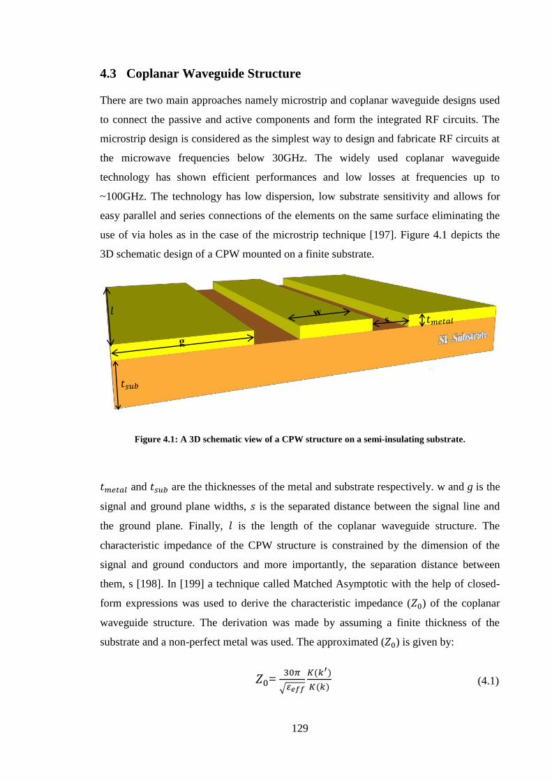
129
4.3 Coplanar Waveguide Structure
There are two main approaches namely microstrip and coplanar waveguide designs used
to connect the passive and active components and form the integrated RF circuits. The
microstrip design is considered as the simplest way to design and fabricate RF circuits at
the microwave frequencies below 30GHz. The widely used coplanar waveguide
technology has shown efficient performances and low losses at frequencies up to
~100GHz. The technology has low dispersion, low substrate sensitivity and allows for
easy parallel and series connections of the elements on the same surface eliminating the
use of via holes as in the case of the microstrip technique [197]. Figure 4.1 depicts the
3D schematic design of a CPW mounted on a finite substrate.
Figure 4.1: A 3D schematic view of a CPW structure on a semi-insulating substrate.
𝑡𝑚𝑒𝑡𝑎𝑙 and 𝑡𝑠𝑢𝑏 are the thicknesses of the metal and substrate respectively. w and g is the
signal and ground plane widths, 𝑠 is the separated distance between the signal line and
the ground plane. Finally, 𝑙 is the length of the coplanar waveguide structure. The
characteristic impedance of the CPW structure is constrained by the dimension of the
signal and ground conductors and more importantly, the separation distance between
them, s [198]. In [199] a technique called Matched Asymptotic with the help of closed-
form expressions was used to derive the characteristic impedance (𝑍0) of the coplanar
waveguide structure. The derivation was made by assuming a finite thickness of the
substrate and a non-perfect metal was used. The approximated (𝑍0) is given by:
𝑍0= 30𝜋
√𝜀𝑒𝑓𝑓
𝐾(𝑘′)
𝐾(𝑘) (4.1)

130
𝐾(𝑘) is the elliptic integral of the first kind, 𝑘 is calculated from the dimension of CPW
structure and given by:
𝑘 =𝑤
𝑤 + 2𝑠 (4.2)
Moreover, 𝑘′ is complementary of 𝑘 and given by:
𝑘′ = √1 − 𝑘2 (4.3)
휀𝑒𝑓𝑓 =휀𝑟 + 1
2 (4.4)
where 휀𝑒𝑓𝑓 and 휀𝑟 are the effective and relative permittivities of the substrate. In a real
CPW structure, the electromagnetic wave travels through the dielectric part of the
substrate and air. Hence the wave is hosted by two mediums with different propagation
and permittivity performances. Therefore, if equation 4.4 is used, the total average
permittivity is used and accurate estimation of the characteristic impedance is thus
achieved. In this work, the design and optimisation of the CPW matching circuits and
transmission lines were carried out using the Linecalc tool embedded in ADS software.
The tool also can be used to calculate the dimension of the microstrip and grounded
CPW structure at a given frequency and characteristic impedance. The characteristic
impedance of the CPW structure can be well controlled, and thus, a minimum loss is
achieved if the optimum conditions are met. The next section addresses the limitation and
design consideration of such structures.
4.4 Characteristic Impedance and Attenuation of CPW Structure
As mentioned before, the CPW structure is the most used technique for the mm-wave
MMIC circuits. For a practical and low loss CPW, it is vital to understand how the CPW
structure performs at a high frequency of operation. The attenuation of the CPW structure
is mainly due to the introduced losses in the conductor lines and the dielectric part of the
substrate and more importantly due to the radiation losses caused by the variation of the
dielectric permittivity with frequency.

131
4.4.1 Conductor Loss
Conductor loss is a frequency-dependent mechanism which depends strongly on the skin
depth of the metal and the dimension of the CPW structure (w and s). The frequency
dependent skin depth factor is given by:
δ = √𝜌
𝜋𝑓µ0µ𝑟 (4.5)
where 𝜌 is the resistivity of the metal, µ0 is the free space permeability and equal to
4π×10−7 Henry/meter, µ𝑟 is the relative permeability and equal to 1, 𝑓 is the lowest
operating frequency. The metal thickness 𝑡𝑚𝑒𝑡𝑎𝑙 is usually made with a thickness that is
threetofivetimestheskindepthδof the film which greatly minimises the attenuation
inside the conductor [199]. Conductor loss increases with smaller signal width, w, and
larger separation distance, s or vice versa. Experimental and theoretical works were
carried out in [180] to investigate the effect of varying w and s on the conductor loss of
the CPW structure. It was found that for 0.4 < 𝑘 < 1, the conductor loss is small and can
be neglected at low-frequency regimes. Another important factor is mesa area contact
losses due to the impact of eddy current, which is important at high frequencies [191].
The generation of eddy current in the mesa area contact comes from the time-varying
magnetic field around the anode bridge. Eddy current loss increases proportionally with
the square of the operating frequency 𝑓.
4.4.2 Dielectric and Radiation Losses
Dielectric loss in (dB/m) on the other hand, increases with the loss tangent (𝑡𝑎𝑛𝛿) of the
substrate as expressed in the following equation:
𝛼𝑑(𝑑𝐵/𝑚) = 𝑎𝜋𝑡𝑎𝑛𝛿
𝜆0
휀𝑟
√휀𝑒𝑓𝑓
휀𝑒𝑓𝑓 − 1
휀𝑟 − 1 (4.6)
where a=8.86, 𝜆0 is the free space wavelength. GaAs and InP substrates have very low
loss tangent of 0.0016 and 0.002 respectively, making them appropriate materials for the
implementation of the mm-wave and the sub-mm-wave integrated circuits.

132
The most critical loss mechanism is the radiation loss at higher frequencies caused by the
CPW field overlap with surface wave modes. Well-controlled design steps reduce the
loss to its minimum level. The separation distance (𝑤 + 2𝑠) has a high impact on the
attenuation of the guided waves inside the dielectric substrate as given by the following
expression [200]:
𝛼𝑟 = 𝑓(휀𝑟)(1
𝜆𝑑)3
(𝑤 + 2𝑠)2
𝐾(𝑘)𝐾(𝑘′) (4.7)
where 𝜆𝑑 is the dielectric wavelength and given by:
𝜆𝑑 =𝑐
𝑓√휀𝑟 (4.8)
where c is the speed of light in vacuum, and 𝑓(휀𝑟) is expressed by:
𝑓(휀𝑟) = (𝜋
2)5
1
√2
(1 −1휀𝑟
)2
√1 +1휀𝑟
(4.9)
For a 50Ω CPW structure sits on semi-insulator GaAs substrate with a 𝑘~0.5, equation
4.7 is reduced to the following form:
𝛼𝑟 = 13.8(𝑤 + 2𝑠
𝜆𝑑)2 (4.10)
The freedom of changing (𝑤 + 2𝑠) in CPW structure helps to mitigate the field
interaction with the surface mode while keeping the impedance of the line constant. If
(𝑤 + 2𝑠) is made to be much smaller than the substrate thickness and dielectric
wavelength, a minimum radiation loss is thus obtained. The designed 50Ω CPW
structures on a GaAs platform used in this work have shown as small attenuation as
~0.05dB, corresponding to (𝑤 + 2𝑠) of 120µm and 𝜆𝑑 of ~2mm at a wave frequency of
40GHz. Making the designed CPW structure a suitable technique for mm-wave MMIC
integrated circuits. However, the effect of the surface wave and dispersion has to be
taken into account when the dielectric wavelength is comparable to (𝑤 + 2𝑠) at high-
frequency regimes. 3D simulators such as CST studio and EMpro from Keysight as well

133
as the momentum microwave simulation account for such losses as the effect of the
surface wave mode is considered in their calculations.
4.5 MMIC Metal-Insulator-Metal Capacitor
The capacitor is a passive component used in microwave and RF circuit in the form of
passing or blocking signals. The mechanism relies on capacitance value and frequency,
which both determine the impedance of the capacitor. In the literature, two simple
approaches have been successfully employed to design and fabricate capacitors for RF
integrated circuits; interdigital and MIM capacitors. The top view of the interdigital
capacitor in figure 4.2 shows the metal fingers and the separation between them, which is
usually a few microns. Its advantage comes from the fabrication simplicity and
insensitivity to process variations [175, 201]. However, due to the fingers size and
separation distance limitations, interdigital capacitor values are low and limited to a
maximum value of ~1pF. Such capacitance cannot be exploited in the integration of mm-
wave detectors as the required capacitance has to be > 1pF to suppress the RF signal and
the generated harmonic tones. Moreover, the large size makes it incompatible for
implementation in small RF circuits [193]. Furthermore, a small separation distance leads
to more coupling effect between fingers in which parasitic elements are introduced in the
MMIC integrated circuits.
Figure 4.2: Layout representation of nine-fingers interdigital capacitor [193].

134
MIM capacitors, on the other hand, have been fabricated with a capacitance value
ranging from 50fF to 200pF. A MIM capacitor is formed of a dielectric layer sandwiched
between two metal plates, as shown in figure 4.3. The capacitance value is calculated
from the thickness and permittivity of the dielectric layer as well as the active overlapped
area between plates using the expression (𝐶 = 휀0휀𝑟𝑤𝑙/𝑑).
Figure 4.3: 3D view of the MIM capacitor.
There are wide varieties of materials used as insulator layers such as benzocyclobutene
(BCB), SiO2, and Si3N4 which have permittivities of 2.7, 3.9, and 7.5 respectively were
reported in the literature. The latter has been widely used compared to other materials as
it has a high breakdown voltage (exceeding 65V) and low dielectric loss [175]. In this
work, MIM capacitors with a 200nm Si3N4 dielectric thickness were designed and
integrated with the ASPAT detector circuits. Figure 4.4 (a) shows the discrete rectangular
layout structure of a 10pF capacitor of an active overlapping metal area of 180×180µm².
In the literature, the equivalent circuit of the CPW MIM capacitor was demonstrated,
showing the associated parasitic elements with the main capacitor as depicted in figure
4.4 (b) [202, 203].

135
(a)
CMIM
G
LaRa Rb
Lb
CaCbDielectric losses
(b)
Figure 4.4: (a): 10pF CPW MIM capacitor used in this work (b): Equivalent circuit model of MIM
capacitor [202].
𝑅𝑎 , 𝑅𝑏, 𝐿𝑎, 𝐿𝑏, 𝐶𝑎, 𝐶𝑏 are the parasitic resistance, inductance, and capacitance elements
respectively introduced by the top and bottom plates. The conductance loss introduced by
the dielectric is given by [202]:
𝐺 = 2𝜋𝑓𝐶𝑀𝐼𝑀𝑡𝑎𝑛𝛿 (4.11)
where 𝐺 is a frequency dependent conductance that represents the increase of the leakage
current through the dielectric as the frequency increases. The discrete capacitance was
firstly simulated using the momentum (MoM) microwave simulation tool to verify the
design and to optimise the dimensions for minimum parasitic losses. It can be said that
the MoM simulation tool gives a good prediction of the capacitor behaviour (black line)

136
over the frequency range 40MHz to 40GHz, as shown in figure 4.5. The small difference
(~10%) between the measured and MoM simulation results could be attributed to the
losses of the measurement cables and GSG input port. Using the equivalent circuit
model, the main capacitance value was found to be ~8pF instead of 10pF. Figure 4.5
shows a good fit between the measured (red line) and simulated (blue line) S-parameters
extracted from the equivalent circuit models. The conductance loss (𝐺) was neglected as
𝑡𝑎𝑛𝛿 of the dielectric used is relatively small (0.0003). The fitting process also yields the
following parasitic components; 𝑅𝑎 , 𝑅𝑏=2.66Ω, 𝐿𝑎, 𝐿𝑏=17pH, 𝐶𝑎, 𝐶𝑏=22.5fF. The
extracted parasitic resistances of our MIM capacitors are close enough to the reported
values in [203].
10 20 30 40
-25
-20
-15
-10
-5
0
10 20 30 40-10
-5
0
5
S1
1 (
dB
)
Frequency (GHz)
Measured
Equivalent Circuit
MoMS
12 (
dB
)
Frequency (GHz)
Measured
Equivalent Circuit
MoM
Figure 4.5: Measured, equivalent circuit, and MoM S-parameters results of 10pF CPW MIM
capacitor.
4.6 Matching Networks
Matching circuits are necessary elements for detector and mixer circuits to eliminate the
mismatch between standard 50Ωsource anddiode impedance.Proper matching means
more power will be delivered to the diode and thereby improving detector or mixer
performances. The matching circuit also mitigates the leakage power from one port to
another in mixer circuits. Lumped elements have been extensively employed in matching
networks up to 1GHz [69]. For mm-wave and sub-mm-wave applications, a matching

137
circuit is usually implemented using two stubs network. These stubs can be either open
or short type, as shown in figure 4.6 [66].
Transmission line Stub
Short Stub
Input Output
Open Stub
Figure 4.6: Matching circuit using open and short stubs [66].
Open stubs are preferred in the case of microstrip line circuit, unlike the short that is used
in coplanar waveguide technology due to the ease of implementation. The matching
circuit works as a kind of narrowband filter. In a single input port circuit (such as
detector), matching circuit implementation is straightforward and requires few steps to
optimise its performances. In mixers, more steps and iteration processes are required to
achieve the minimum reflections.
In most cases, the designed matching circuit cannot provide proper matching at all ports
and frequencies. Since the conversion occurs for the RF signal, it is essential to pay more
attention to the RF side matching circuit. However, using stubs for termination purpose
affect the impedance seen by the sources on both sides. The MMIC CPW open and short
stubs are commonly realised as depicted in figure 4.7.
Figure 4.7: Open and short stubs using CPW transmission lines [204].
w s

138
The open and short stubs can be viewed as resonator circuits composed of LCR
components in series and parallel connections, respectively. The length 𝑙 of the open and
short stubs can be theoretically estimated using the following equation [198, 205]:
𝑙 =𝑐
4𝑓𝑟√휀𝑒𝑓𝑓
− 𝑙𝑒𝑥𝑡 (4.12)
where 𝑐 is the speed of light, 𝑓𝑟 is the resonant frequency. One important limitation in the
design of the CPW stub is the parasitic extension length (𝑙𝑒𝑥𝑡). 𝑙𝑒𝑥𝑡−𝑜𝑝𝑒𝑛 is used for the
open CPW stub which describes the impact of parasitic fringing capacitance (𝐶𝑓𝑟𝑖𝑛𝑔𝑖𝑛𝑔)
due to the fringing field effect at the gap distance a. 𝑙𝑒𝑥𝑡−𝑜𝑝𝑒𝑛 is defined as the ratio
between the fringing capacitance (𝐶𝑓𝑟𝑖𝑛𝑔𝑖𝑛𝑔) to the main capacitance of the CPW open
stub (𝐶𝑠𝑡𝑢𝑏). It was indicated in [204] that 𝐶𝑓𝑟𝑖𝑛𝑔𝑖𝑛𝑔 can be substantially reduced and thus
𝑙𝑒𝑥𝑡−𝑜𝑝𝑒𝑛 by making the separation distance a equal or larger than (𝑤 + 2𝑠). In this case,
𝑙𝑒𝑥𝑡−𝑜𝑝𝑒𝑛 can be approximately calculated from the dimension of the CPW using the
expression [204]:
𝑙𝑒𝑥𝑡−𝑜𝑝𝑒𝑛 = 0.25(w + 2s) (4.13)
On the other hand, 𝑙𝑒𝑥𝑡−𝑠ℎ𝑜𝑟𝑡 of the short CPW stub is given by the ratio of end
inductance (𝐿0) to the inductance of the line stub (𝐿𝑠𝑡𝑢𝑏). 𝐿0 comes from current
circulation in the discontinuity region [206]. The study conducted in [206] investigated
the performances of short CPW stubs, where it experimentally proved the strong
dependence of 𝑙𝑒𝑥𝑡−𝑠ℎ𝑜𝑟𝑡 on the metal thickness 𝑡𝑚𝑒𝑡𝑎𝑙 of the pads. If the metal thickness
was in the range 1 to 3µm, the impact of 𝑙𝑒𝑥𝑡−𝑠ℎ𝑜𝑟𝑡 is small and can be neglected. With
this in mind, 𝑙𝑒𝑥𝑡−𝑠ℎ𝑜𝑟𝑡 can be found using the approximated formula [206]:
𝑙𝑒𝑥𝑡−𝑠ℎ𝑜𝑟𝑡 = 0.125(w + 2s) (4.14)
Generally speaking, short stubs offer better performances since they have less parasitic
effects compared to open stubs.

139
4.7 Modelling of ASPAT I-V Characteristics
The cornerstone of the detection circuit is the non-linear element, and therefore, much
care must be paid to build a virtual model which accurately behaves like the real
fabricated device. Due to the lack of a built-in tunnel diode model in the Keysight ADS
library, a polynomial representation method was used in this work to model and
implement the measured non-linear characteristics of the ASPAT diodes. The method has
been widely used by other researches to model the non-linear characteristics of RTD and
transistor devices [66, 207]. The Symbolically Defined Devices (SDD) model embedded
in ADS was successfully employed to model the non-linear I-V characteristics of the
ASPAT diodes which can then be used in the non-linear simulation of the high-frequency
detector and mixer circuits. The SDD model is considered as an alternative approach to
the built-in model and was successfully validated by many researchers [66, 207]. The
generation of the polynomial equation was performed using the Matlab software. Due to
the small measured current at bias around the zero-operation region, the measured I-V
curve was segmented into small regions, and then the polynomial equation was
developed for each part. This way ensures a highly accurate modelling of the DC
characteristics, and hence, an optimum fitting with the measured data at all bias is
achieved. Once the optimum polynomial equation was found, the coefficients were
imported to the SDD block, and the model was created. Figure 4.8 (a) depicts the
schematic representation of the two-port SDD model used in this work. The measured I-
V characteristics involve the effect of the series resistance in addition to the non-linear
junction resistance. For real circuit simulation, resistance in series was added which
accounts for the total series composed of (𝑅𝑆+𝑅𝑢) to accurately model the input
impedance of the ASPAT diode. An example of the measured and fitted I-V curves is
presented in figure 4.8 (b).
SDD model demonstrated a well-matched non-linear transition at zero-bias, which is the
key region for zero-bias circuits. Accurate representation can be well-achieved by
generating a high order polynomial equation for each part of the I-V curve. However, a
challenging issue occurs as the mesa area decreases due to the limitation of the
polynomial equation to model the small current (nA ranges) of the diodes. Any variation
between the measured and modelled I-V characteristics leads to having different junction
resistance and curvature coefficient, which results in a bad prediction of the whole
integrated circuit performance.

140
(a)
-1.0 -0.5 0.0 0.5 1.010
-6
10-5
10-4
10-3
10-2
10-1
Cu
rren
t (m
A)
Voltage (V)
Measured
SDD fit
(b)
Figure 4.8: (a): Two-port SDD model circuit in ADS tool, (b): Measured and fitted curves of the
3.7×3.7µm² GaAs/AlAs ASPAT diode.

141
4.8 Schematic Design and Simulation of Detectors and Mixers using
ADS Tool
The schematic design tool represents the first platform to start the design of MMIC
integrated circuits. The work conducted in this thesis was mainly performed using the
ADS tool provided by Keysight technology. The tool includes a set of built-in models of
various diodes and transistors. In this work, schematic and layout designs were used to
model the non-linear characteristics of the ASPAT diodes, single passive elements, as
well as the whole integrated circuits. The schematic ADS design is a powerful tool which
offers a wide variety of linear and non-linear time and frequency domain simulators. For
example, the harmonic balance simulator is used to simulate the non-linear
characteristics of the direct and heterodyne detection systems such as the 1-dB
compression and third-order intercept point. Once a good SDD model was found, the
next step was the design process of the matching circuit. The aim was to use a coplanar
waveguide technology to realise the matching circuit and the MMIC integrated circuits.
The design step of the matching circuit is an iterative process and started by calculating
the diode impedance seen by the input ports.
At some power level, the diode impedance is either too large or too small, which makes
the design of the matching circuit extremely difficult. In this work, we mainly focused on
the GaAs/AlAs ASPAT as a promising device for commercial zero-bias detectors at X-
band and K-band frequencies. In the beginning, RF signals were applied, and diode
impedances were obtained at the desired power and frequency RF signal. Larger mesa
area size ASPAT diodes (5.8×5.8µm² and 10×10µm²) were fed by a 10GHz RF signal,
while a 24GHz RF signal was applied to the 3.7×3.7µm² ASPAT diode. Impedances
were found to be ~24 − 𝑗316Ω, ~14 − j296Ω, and ~7.7 − j115Ω for the 3.7×3.7µm²,
5.8×5.8µm² and 10×10µm² mesa area sizes respectively. The imaginary part of the
impedance can be theoretically estimated using the expression 𝑗/𝜔𝐶𝐽. Thereafter, the
‘smithcharttool‘ embedded in ADS was exploited to build the matching circuit of every
single diode. The tool uses lumped elements and stubs to realise the matching network.
Ideal short stubs were used to form the CPW matching circuits as they have less parasitic
effects as discussed earlier. An example of the schematic design of the zero-bias ASPAT
detector using ideal transmission line stubs is depicted in figure 4.9 (a). The output DC
voltage is taken across the output capacitor (10pF). Similar steps were carried out to
build the matching circuits of the subharmonic mixers at different frequencies of the

142
input RF signal. In 2nd
subharmonic mixer circuits, as shown in figure 4.9 (b), matching
circuits were designed and optimised using three steps.
(a)
(b)
Figure 4.9: (a): Zero-bias direct detection circuit based 5.8×5.8µm² GaAs/AlAs ASPAT diode, (b):
Zero-bias 2nd
subharmonic mixer based 3.7×3.7µm² GaAs/AlAs ASPAT diode.
Firstly, the impedance was calculated at the RF side, and a matching circuit was built at
the desired RF power and frequency signal. Secondly, the impedance at the LO side was
RF
side
LO
side
Anti-parallel ASPAT
diodes
IF
side

143
evaluated, which includes the sum of anti-parallel ASPAT diodes and RF matching
impedances. Then a proper matching circuit was designed and inserted at the LO side. At
this point, the RF side sees different impedance value due to the inclusion of LO
matching circuit. Therefore, the last step was to repeat the design of the matching
network at the RF side as the RF signal has lower power compared to the LO signal, so it
is crucial to make sure that the RF side is not affected by the matching circuit at the LO
side.
Testing and optimising the ideal transmission line detector and mixer circuits were
carried out to minimise the reflections further and improve the performances as much as
possible. The primary simulation tool used was the well-known Harmonic Balance (HB)
block. The tool provides practical calculations of the mixing process of the main signals
as well as their high order harmonic components. It is noteworthy to state here, that an
appropriate setting of the HB block plays a vital role in calculating the desired output
current and voltage. An accurate simulation of mixers depends on the order of the
harmonic component of the RF and LO signals set in the (HB) block. In our simulation,
high order harmonic components were used with the LO signal since it has higher power
compared to RF signal and so it is assumed to have a significant influence on the output
frequency spectrum. The polynomial equation used in the SDD model is limited to a
range of voltages, and thus, applying a signal with relatively high power could lead to
unexpected behaviour of the non-linear characteristics of the ASPAT model. Bandpass
filters were used to decrease the level of harmonics that surround the RF and LO signals
and improve the isolation between ports. The filters were located after the LO and RF
sources and before the matching circuits.
4.9 Mask Layout of the MMIC Integrated Zero-Bias ASPAT Detectors
The key next step was to design and optimise the CPW matching circuits and the circuit
layouts for the final fabrication process. CPW short stubs firstly replaced the ideal
transmission lines. CPW dimensions were calculated using the ‘‘LineCalc’’ tool
embedded in the ADS software. The tool offers a wide range of analytical models to
calculate the physical model and electrical parameters of different transmission
technology such as microstrip, CPW, and CPWG structures. Tuning and optimisation of
transmission lines were performed, and then the total behaviour of the CPW stubs was

144
compared with the ideal one. An example of an ideal and CPW short stub matching
circuits of 5.8×5.8µm2 ASPAT detector is shown in figure 4.10.
8 9 10 11 12-40
-30
-20
-10
0
S1
1(d
B)
Frequency (GHz)
Ideal stubs
CPW stubs
Figure 4.10: Matching circuit response of ideal and CPW stubs.
Both responses have a very narrow bandwidth of ~0.2GHz. The CPW stubs behaviour
was as close as possible to the ideal stubs with only ~0.3GHz frequency difference. The
long length of the designed matching circuits are (2.5mm) and (6.5mm), which makes
them not practical for compact RF circuits at X-band and mm-wave frequency
applications. For this reason, all matching circuits were optimised to have a maximum
size of 2×2mm². Following that, all matching circuits were transferred from the
schematic platform to the layout representation. As there is no CPW T-junction model
embedded in ADS library, the T-junction was optimised through an iterative process to
obtain the desired behaviour. Matching circuits were designed with a GSG input port
configuration and conductor width of 50µm.
The separation between the conductor and the grounds was made to be 35µm. The
designed matching circuits can be grouped into two parts: X-band and K-band CPW
networks. The moderate junction resistance (35 to 50kΩ) and high cut-off frequency
(~245GHz) of the 5.8×5.8µm2 ASPAT made it an excellent choice for the X-band and K-
band frequencies with a small matching circuit size. Four matching circuits were

145
designed and optimised on a 625µm semi-insulating substrate using the momentum
simulation microwave mode. The matching circuit was exported from the layout design
to the schematic design for the final evaluation of the ASPAT detectors performances.
The circuit shown in figure 4.11 was used to evaluate the total performance of the
ASPAT detector with its matching circuit and MIM capacitor layout designs. Once the
maximum performances were achieved, the designs of the mask layouts of the whole
integrated zero-bias ASPAT detectors were carried out for the final fabrication.
Figure 4.11: Final zero-bias ASPAT detector circuit implementation showing the layout design of the
matching circuit and MIM capacitor.
The mask design steps are explained in figure 4.12. Step 1, 2, and 3 shows the definition
of the top and bottom contacts layers as well as the isolation layer to cover the active
layers and the TLM structures. Step 4 defines the Si3N4 layerand therequiredvia’s of
the top contact and MIM capacitor top contact. Step 5 adds the matching circuit and
bottom contact of the MIM capacitor. For this work, 𝐷𝑠𝑝𝑟 was designed to be 1.5µm for
all detector circuits. It is worthy to point out that the input and output ports are designed
with50Ωstandardcharacteristic impedanceexploitingCPWtechnology.However, the
matching circuit topology is an optimised shorted stub simulated using ADS Momentum
taking into account the impact of electromagnetic field coupling on the circuit
performance. The length and width of the centre signal transmission line and stub
provide the desired frequency matching band.

146
Bottom Contact
Top
Step 1, 2, and 3 Iso
latio
n la
yer
Top Via
Via for top contact of MIM
capacitor
Si3N4
Step 4
6µm
6µ
m

147
Figure 4.12: An example of mask design steps of the MMIC zero-bias ASPAT detector of the mesa
area size of 6×6µm².
4.10 Fabrication and Measurement of the MMIC Integrated Zero-Bias
ASPAT Detectors
The fabrication of the ASPAT detector circuits took place in a class 1000 clean room. A
wafer tile of size 15×15mm2 was fabricated into many ASPAT detectors. The fabrication
processes of the detectors were accomplished as follow. Firstly, the definition of the top
mesa area size was carried out by deposition of ~260nm of a metal stack of AuGe/Ni/Au
to form the ASPAT diode top contact. Secondly, an etch down to the ohmic bottom
(GaAs) layer was performed using the etchant H3PO4:H2O2:H2O with a ratio of 3:1:50
followed by deposition of 260nm of AuGe/Ni/Au metal to form the bottom contact of the
Strip line
MIM bottom
Contact
MIM Top
Contact
Step 5
Matching network

148
ASPAT diode and the MIM capacitor top contact. Thirdly, an isolation step is performed
by covering the active layers and the TLM structures with photoresist coating and then
etching down to the substrate. Fourthly, for the DC signal output voltage, a 200nm Si3N4
dielectric layer was sputtered on the whole wafer tile. The designed MIM capacitor
whose size was 180×180µm² provided a 10pF value which is adequate to suppress the
RF current at X-band frequencies and the generated frequency tones associated with the
diode output current signal. The required vias for the top contact of the ASPAT and MIM
capacitor were opened in a subsequent step. Finally, a Ti/Au (50nm/1400nm) metal
deposition of the matching circuit and the bottom contact of the output capacitor were
carried out. Figure 4.13 depicts the fabricated zero-bias ASPAT detectors. The RF signal
transmission line is connected to the bottom ground through a short stub. This ensures
that the ASPAT diode is completely isolated from any DC signal at the input side (to
avoid any self-biasing issue). The capacitor is directly linked to the output GSG port for
reading the generated DC output voltage. Figure 4.13 (a) and (b) depict the 3.8mm² and
2.78mm² X-band detectors based on 5.8×5.8µm² and 10×10µm² ASPAT diodes
respectively. Figure 4.13 (c) and (d) on the other hand present the integrated K-band
detectors of circuit size 0.78mm² and 0.544mm² based on 3.7×3.7µm² and 5.8×5.8µm²
ASPAT devices respectively. The aim of this work was not only to maximise the detector
performances but also to keep the circuit size smaller than 4mm² and 1mm² for the X-
band and K-band frequencies, in which many circuits can be included in the mask layout.
As a result, 76 ASPAT detectors were fabricated on the 15×15mm² wafer tile. Since the
imaginary part of both diodes is relatively high at X-band frequencies, the matching
circuit size was in the millimetre size scale.

149
(a)
(b)
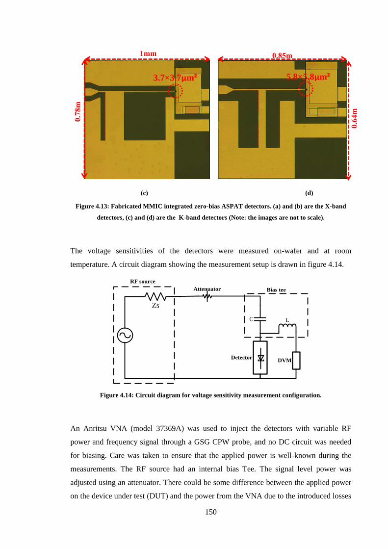
150
(c) (d)
Figure 4.13: Fabricated MMIC integrated zero-bias ASPAT detectors. (a) and (b) are the X-band
detectors, (c) and (d) are the K-band detectors (Note: the images are not to scale).
The voltage sensitivities of the detectors were measured on-wafer and at room
temperature. A circuit diagram showing the measurement setup is drawn in figure 4.14.
Zs
C L
DetectorDVM
Attenuator Bias tee
RF source
Figure 4.14: Circuit diagram for voltage sensitivity measurement configuration.
An Anritsu VNA (model 37369A) was used to inject the detectors with variable RF
power and frequency signal through a GSG CPW probe, and no DC circuit was needed
for biasing. Care was taken to ensure that the applied power is well-known during the
measurements. The RF source had an internal bias Tee. The signal level power was
adjusted using an attenuator. There could be some difference between the applied power
on the device under test (DUT) and the power from the VNA due to the introduced losses
1mm
0.7
8m
m
0.85m
m
0.6
4m
m
3.7×3.7µm² 5.8×5.8µm²
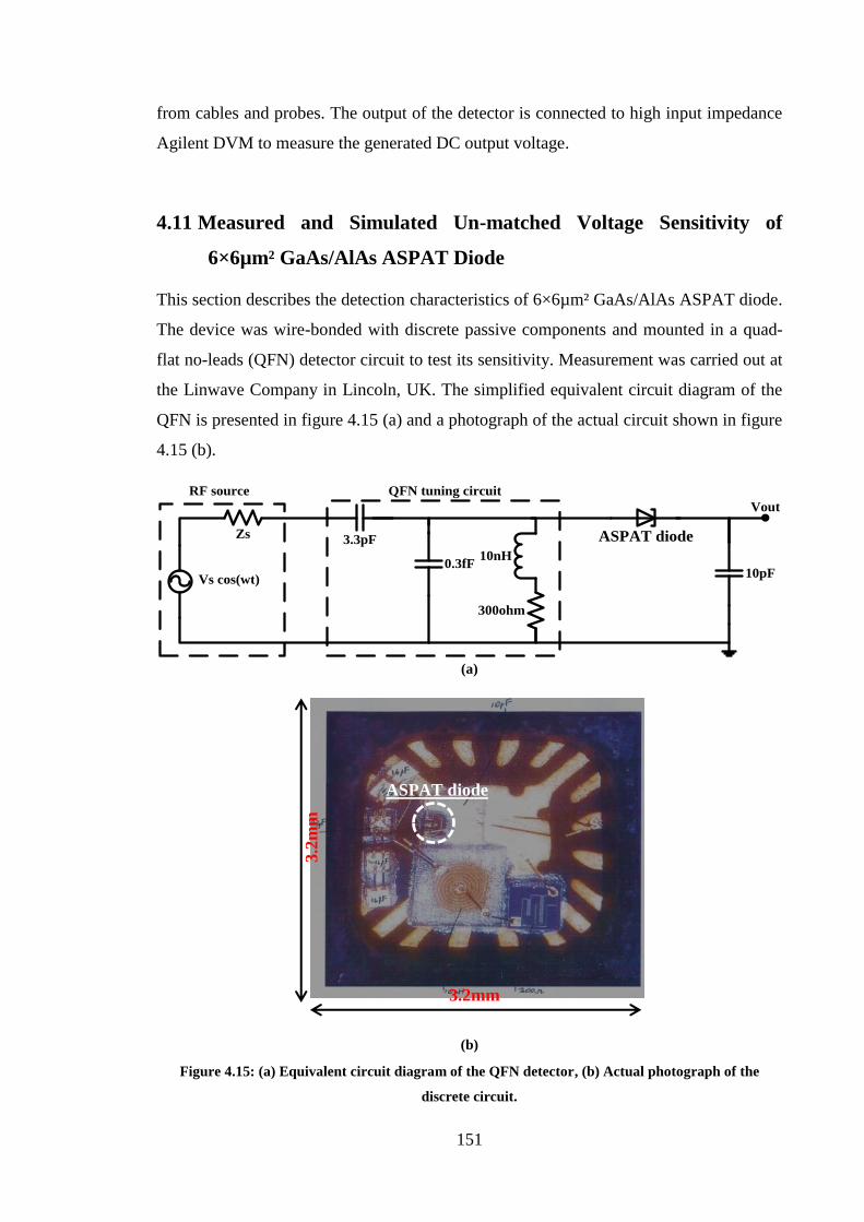
151
from cables and probes. The output of the detector is connected to high input impedance
Agilent DVM to measure the generated DC output voltage.
4.11 Measured and Simulated Un-matched Voltage Sensitivity of
6×6µm² GaAs/AlAs ASPAT Diode
This section describes the detection characteristics of 6×6µm² GaAs/AlAs ASPAT diode.
The device was wire-bonded with discrete passive components and mounted in a quad-
flat no-leads (QFN) detector circuit to test its sensitivity. Measurement was carried out at
the Linwave Company in Lincoln, UK. The simplified equivalent circuit diagram of the
QFN is presented in figure 4.15 (a) and a photograph of the actual circuit shown in figure
4.15 (b).
0.3fF10nH
300ohm
3.3pF
10pFVs cos(wt)
Zs
Vout
RF source QFN tuning circuit
ASPAT diode
(a)
(b)
Figure 4.15: (a) Equivalent circuit diagram of the QFN detector, (b) Actual photograph of the
discrete circuit.
ASPAT diode
3.2mm
3.2
mm

152
The circuit is simple and consists of a fixed R-L-C circuit placed between the input RF
signal and the mounted ASPAT diode. The RLC circuit works as a tuning matching
circuit. However, it has no matching purpose to the ASPAT diode. R, C, and L values
were tuned to obtain the maximum output voltage. A fixed frequency signal of 9.5GHz
was applied to the ASPAT diode. The power was swept from -35 to -5dBm, and
accordingly, the output voltage was measured on the output capacitor (10pF). The circuit
was simulated in the ADS tool, and its voltage sensitivity compared with the measured
one, as shown in figure 4.16. The bond pad effect was represented in the circuit by
including 𝐶𝑃 and 𝐿𝑃 for accurate simulation process. The simulated sensitivity is in
excellent agreement with the measured one, and this validates the SDD model and the
modelled circuit used to design and model the ASPAT detector. Moreover, it also
verifies the extracted parameters of the ASPAT diode (𝐶𝐽,𝑅𝐽, and 𝑅𝑆) which were used in
the model. The 6×6µm² ASPAT device exhibited a voltage sensitivity of 950V/W at
9.5GHz and -30dBm RF power. The inset shows the measured video resistance (𝑅𝐽 + 𝑅𝑆)
as a function of the input RF power. The measured resistance is ~30kΩ at a low input RF
power of -35dBm and gradually decreases to ~10kΩat an RF power of 0dBm.
-30 -20 -10 0200
400
600
800
1000
-30 -20 -10 05
10
15
20
25
30
35
Un
-matc
hed
Volt
age S
en
siti
vit
y (
V/W
)
Input RF power (dBm)
Measured
Simulated
@ 9.5GHz
Vid
eo R
esi
stan
ce (
k
)
Input RF power (dBm)
Figure 4.16: Measured and simulated un-matched voltage sensitivity of 6×6µm² ASPAT diode. The
inset is the measured video resistance.

153
To investigate the maximum voltage sensitivity of the zero-bias GaAs/AlAs ASPAT
diodes; ideal transmission line matching circuits were designed, and the fully matched
voltage sensitivities were simulated. These showed that the 3.7×3.7µm² and 5.8×5.8µm²
GaAs/AlAs ASPAT diodes have a maximum voltage sensitivity of ~20000V/W and
~7500V/W respectively at 24GHz RF signal. Voltage sensitivity of ~9000V/W at 10GHz
was obtained using the 10×10µm² ASPAT diode at zero-bias.
4.12 ASPAT Detectors Performances
This section reports the measured and simulated voltage sensitivity in addition to the
calculated noise equivalent power of the fabricated integrated zero-bias ASPAT
detectors. The main goal was to investigate the voltage sensitivity and verify the
proposed detector models.
4.12.1 Measured DC Output Voltage
The output voltage (𝑉𝑜𝑢𝑡) of the fabricated detectors were measured in the frequency
bands [4 to 18GHz] and [10 to 35GHz] at RF power ranging from -27 to -4dBm. The
measured 𝑉𝑜𝑢𝑡 of ASPAT detectors versus frequency at -27dBm RF power are shown in
figure 4.17. The figure shows good voltage uniformity over five ASPAT detector circuits
at different locations on the wafer tile. It also validates the successful modelling and
fabrication of the MMIC integrated ASPAT detectors. The 5.8×5.8µm² and 10×10µm²
ASPAT detector circuits showed excellent output voltage over the bandwidth [5 to
6.5GHz] covering the X-band frequencies. At X-band frequencies, the 5.8×5.8µm²
ASPAT diode provided a better output voltage of ~7.5mV at ~11GHz compared to
~2.7mV for the 10×10µm² ASPAT at 9.5GHz as depicted in figure 4.17 (a) and (b). The
higher output voltage is due to smaller junction capacitance and better matching
condition of the 5.8×5.8µm² ASPAT diode corresponding to a smaller reflection
coefficient of -12dB at 11GHz as clearly seen in figure 4.17 (c). The high reflection
coefficient of the 10×10µm² ASPAT arises from the large junction capacitance which
gives a weak prediction process of the matching circuit behaviour. Undoubtedly, more
optimisation of the matching circuit stubs is necessary to reduce the reflection coefficient

154
of the detector and obtain higher output voltage. Figure 4.17 (d) and (e) show excellent
bandwidths of ~9GHz covering the K-band frequencies [18 to 26.5GHz].
4 6 8 10 12 14 16 180
2
4
6
8
4 6 8 10 12 14 16 180
1
2
3
10 15 20 25 30 350
1
2
3
10 15 20 25 30 350
1
2
3
4 6 8 10 12 14 16 18
-12
-10
-8
-6
-4
-2
0
10 15 20 25 30 35-25
-20
-15
-10
-5
0
5.8x5.8m2 ASPAT
Vo
ut (m
V)
Frequency (GHz)
Circuit1
Circuit2
Circuit3
Circuit4
Circuit5
B.W=5GHz
B.W=9GHz
B.W=9.5GHz
10x10m2 ASPAT
Vo
ut (m
V)
Frequency (GHz)
Circuit1
Circuit2
Circuit3
Circuit4
Circuit5
B.W=6.5GHz
3.7x3.7m2 ASPAT
Vo
ut (
mV
)
Frequency (GHz)
Circuit1
Circuit2
Circuit3
Circuit4
Circuit5
10-35 GHz
(f)
(e)
(d)
(c)
(b)
(a)
5.8x5.8m2 ASPAT
Vo
ut (m
V)
Frequency (GHz)
Circuit1
Circuit2
Circuit3
Circuit4
Circuit5
4-18 GHz
S1
1 (
dB
)
Frequency (GHz)
5.8x5.8m2 ASPAT
10x10m2 ASPAT
S1
1 (
dB
)
Frequency (GHz)
3.7x3.7m2 ASPAT
5.8x5.8m2 ASPAT
Figure 4.17: (a), (b), and (c) are the measured output DC voltage and reflection coefficients (𝑺𝟏𝟏) of
the X-band zero-bias detectors based 5.8×5.8µm² and 10×10µm² GaAs/AlAs ASPAT diodes at -
27dBm RF power. (d), (e), and (f) are the measured output DC voltage and reflection coefficients
(𝑺𝟏𝟏) of the K-band zero-bias detectors based 3.7×3.7µm² and 5.8×5.8µm² GaAs/AlAs ASPAT diodes
at -27dBm RF power.

155
The 3.7×3.7µm² and 5.8×5.8µm² ASPAT achieved an output voltage of ~2.5mV at
~24GHz. It is clear that both detectors have a good response with a reflection coefficient
of < -20dB at the K-band frequencies in the case of the 5.8×5.8µm² ASPAT detector. The
5.8×5.8µm² ASPAT diode was found to be more suitable for the K-band frequencies due
to its smaller junction resistance compared to the 3.7×3.7µm² ASPAT device.
Accordingly, 5.8×5.8µm² ASPAT detectors have a better reflection coefficient response
at the 24GHz frequency. In conclusion, the maximum output voltage of the detector is
constrained by the matching circuit behaviour, junction resistance, and junction
capacitance. More importantly, the parasitic effect of the matching circuit was not
considered in our calculation and design process, which have a higher impact on the K-
band frequencies.
4.12.2 Voltage Sensitivity and Noise Equivalent Power
Voltage sensitivities were then calculated by taking out the average of the measured DC
voltage of different circuits at each input RF power. The noise equivalent power (NEP)
was then computed from the measured sensitivity at a video bandwidth of 1Hz. Figure
4.18 (a) and (b) depict the high correlation between the measured and simulated voltage
sensitivity as well as the calculated NEP of the X-band and K-band zero-bias detectors
based 5.8×5.8µm² ASPAT diode. The excellent correlation validates the model used,
allowing for prediction of performances and aid in further optimisation prior to costly
manufacturing processes. The measured voltage sensitivities were ~1800 to 3650V/W
and 700 to 1300V/W at the X-band and K-band frequencies, respectively. The maximum
measured voltage sensitivity is ~3650V/W at 11GHz and -27dBm RF power which is
comparable to the zero-bias Schottky detector in [208], where a voltage sensitivity of
1000V/W at ~10GHz is reported. The measured voltage sensitivity and junction
resistance were then used to estimate the noise equivalent power using equation (2.20)
provided in chapter two. The calculated NEP was below 14pW/√Hz at X-band
frequencies with a minimum value of ~6pW/√Hz at 11GHz. On the other hand, the K-
band ASPAT detector recorded a noise equivalent power below 35pW/√Hz with a
minimum value of ~20pW/√Hz at 24GHz.

156
-30 -25 -20 -15 -10 -5 0
1000
2000
3000
4000
8 9 10 11 12 130
1000
2000
3000
4000
K-band@ -27dBm
(c)
(a)
Measured Sensitivity
Simulated Sensitivity
Calculated NEP
Frequency (GHz)
Vo
lta
ge S
en
siti
vit
y (
V/W
)
(b)
@ -27dBm X-band
0
5
10
15
20
NE
P (
pW
/sq
rt(H
z))
18 20 22 24 26 280
500
1000
1500
Measured Sensitivity
Simulated Sensitivity
Calculated NEP
Frequency (GHz)
Vo
lta
ge S
en
siti
vit
y (
V/W
)
0
10
20
30
40
50
N
EP
(p
W/s
qrt
(Hz))
Vo
lta
ge S
en
siti
vit
y (
V/W
)
Input RF power (dBm)
Measured at 11GHz
Simulated at 11GHz
Measured at 24GHz
Simulated at 24GHz
Figure 4.18: (a) and (b) are the measured and simulated voltage sensitivity and calculated noise
equivalent power of the X-band and K-band zero-bias detectors based 5.8×5.8µm² ASPAT diode, (c)
is the measured and simulated voltage sensitivity versus input RF power.

157
The zero-bias 5.8×5.8µm² ASPAT diode showed good voltage sensitivity and noise
equivalent power at K-band compared to the biased Schottky detector reported in [209]
despite the much larger mesa area size used in this work (33.6µm² vs 1.3µm²). The
measured voltage sensitivity as a function of input RF power is depicted in figure 4.18
(c). The data demonstrate good linearity, and the detectors can deliver half of the
maximum sensitivity even with a high RF power of -10dBm. The matching circuit was
designed to operate at a relatively low input RF power of -27dBm; as a result, there is a
small difference between the measured and simulated data at RF power higher than -
15dBm. The sensitivity decreases with increasing input power, indicating a transition
from the non-linear region to the linear one at high input power. The zero-bias 10×10µm²
GaAs/AlAs ASPAT detector was also shown to have good sensitivity and NEP of ~800
to 1347V/W and ~11pW/√Hz respectively at X-band and -27dBm RF power. Optimising
the transmission line stubs would improve the detector’s performance, particularly at
high frequencies. Besides that, the use of thinner AlAs barrier ASPAT diode with smaller
junction resistance would also contribute to a further reduction in the NEP of the ASPAT
detector but at the expense of the voltage sensitivity. The main feature of temperature
insensitive operation still gives the ASPAT a tremendous advantage over various other
reported structures. Further increase in voltage sensitivity can be obtained by using
smaller feature sizes or/and high curvature coefficient for efficient mm-wave/THz
frequency regime detector systems. The InGaAs ASPAT diode with thinner AlAs barrier
could also be used for THz detection applications due to its small series resistance and
high cut-off frequency.
It is noteworthy to mention here that work is ongoing in our group to design and fabricate
mm-wave ASPAT detectors at 30GHz, 77GHz, and 90GHz. Different detectors have
been designed with open stub matching networks and then fabricated on a 15×15mm²
GaAs substrate. The preliminary results showed a well-matched data between the
measured and simulated (𝑆11) of the 30GHz integrated ASPAT detector (see
APPENDIX-D). The investigation is in progress to measure their output voltages and
calculate their sensitivities and NEP and these are part of the further work to be
undertaken as a result of this research.

158
4.13 Millimeter-Wave ASPAT Detectors with Antennas
The experimental work described so far presents the rectification performances of the
integrated ASPAT detector using a 50Ω source. In practical systems, the antenna
represents the first element which collects the electromagnetic radiations and then injects
them into the detector circuit for the extraction process. Therefore, it is imperative to
model the ASPAT diode with integrated antenna and investigate the total behaviour.
High gain antennas are highly prefered at mm/THz waves in order to collect the weak
radiation and deliver it to the non-linear element. The horn antenna has the highest ever
achieved gain and efficiency at mm-wave applications but at the expense of large area
size [210]. In the literature [211-213], integrated detectors with different kind of antennas
such as spiral and log-periodic shapes have been proposed showing a wide bandwidth,
high directivity and high voltage sensitivity in mm-wave/THz frequency regions. Among
all types, the bow-tie antenna is widely used in both emitter and detector circuits due to
their simplicity, lightweight, wide bandwidth, and high gain. In [214], a Ka-band
Schottky detector with a bow-tie antenna was fabricated on a 254µm duroid dielectric
substrate. The measured bandwidth of the detector was ~8GHz with a maximum voltage
sensitivity of 510V/W at 31.8GHz frequency. The pHEMT transistor in [215] was
monolithically integrated with a wide bandwidth (~60GHz) bow-tie antenna. A
hyperspherical lens was attached to the back of the substrate to focus the waves on the
antenna. At 250GHz and under 0.3V bias, the maximum measured voltage sensitivity
and calculated NEP were 220V/W and 25pW/√𝐻𝑧 respectively. The work conducted in
[216], introduced a multi-channel detector integrated with high gain and broadband bow
tie antennas at 260 to 400GHz and employing a 0.785µm² Schottky diode. Under 150µA
DC bias, the maximum measured sensitivity and NEP of a single detector were 220 to
330V/W and 60pW/√𝐻𝑧 respectively. Another simple and high gain antenna is the
Quasi-Yagi structure which shows good characterstics at microwave frequenies. The
Quasi-Yagi antennas presented in [217, 218] are deposited on a thick and high dielectric
constant substrate of 640µm and 휀𝑟=10.2, respectively. The antenna works at X-band
with a bandwidth of 4.5GHz and gain of 3 to 7dB. In [219], a Quasi-Yagi antenna with
Schottky detector and matching stubs were designed and optimised for a 24GHz
frequency. The antenna sits on a 254µm duroid dielectric substrate and offers a
bandwidth of 0.7GHz and directivity of 9dB. Different techniques have been proposed to
integrate the antenna in transceiver circuits. The monolithic integration method on the

159
chip is widely exploited by designers to mitigate the mismatch between the components
and thus minimise errors.
This section mainly focuses on the design of bow-tie structures for complete zero-bias
ASPAT detectors with monolithically integrated antennas. The antennas were designed
and optimised for automotive car radar and high-resolution imaging applications at
frequencies of 77GHz and 250GHz, respectively.
4.14 Antenna Design and Performances Evaluation
The bow-tie antennas were designed and simulated using the CST studio electromagnetic
tool at 77GHz and 250GHz frequencies. The structures sit on a 100µm semi-insulating
dielectric GaAs substrate. Figure 4.19 shows the 3D drawing of the proposed integrated
ASPAT detector with bow-tie antenna.
Figure 4.19: A 3D structure of the proposed ASPAT detector with a bow-tie antenna. (Note: image is
not to scale).
The arms of the bow-tie antenna are attached to the heavily doped top and bottom contact
layers of the ASPAT diodes. The gap distance between the arms was ~1.5µm to ensure a
small series resistance.

160
The design of the antennas starts by defining the resonance frequency 𝑓𝑟 and calculating
the dimensions of the structure using the following equations [220]:
𝐿𝐴𝑛𝑡 =1.6𝑐
𝑓𝑟√휀𝑟
(4.15)
𝑊𝐴𝑛𝑡 =0.5𝑐
𝑓𝑟√휀𝑟
(4.16)
𝐿𝑠𝑢𝑏 =𝐿𝐴𝑛𝑡
0.85 (4.17)
𝑊𝑠𝑢𝑏 =𝑊𝐴𝑛𝑡
0.45 (4.18)
In the initial investigations, the bow-tie antenna was designed to work at 250GHz with a
gold thickness of 1µm.
Accordingly, the calculated dimensions are 𝐿𝐴𝑛𝑡 = 534µ𝑚, 𝑊𝐴𝑛𝑡 = 167µ𝑚, 𝐿𝑠𝑢𝑏 =
628µ𝑚, and 𝑊𝑠𝑢𝑏 = 371µ𝑚. Indeed, equations (4.15 to 4.18) were used to design a
bow-tie antenna with CPW input feeding port, as reported in [220] at ~300GHz
resonance frequency. In the beginning, the proposed antennas were designed and
simulated with only the bow-tie arms. Thereafter, transmission lines with output CPW
and CPS pads were then designed and attached to the arms. The structures were
simulated with different GaAs substrate thickness to achieve optimal radiation
performances. Simulation processes have shown optimal characteristics when a substrate
thickness of 100µm is used. It is noteworthy to state that the dimensions of the CPW
pads were optimised through an optimisation process to achieve 50Ω characteristic
impedance compatible with the GSG probe, as shown in figure 4.20.
The inclusion of the transmission lines and the output pads changes the resonance
frequency of the proposed structures. To maintain the 250GHz resonance frequency, the
dimensions of the substrate were optimised to be 𝐿𝑠𝑢𝑏 = 740µ𝑚 and 650µ𝑚 , 𝑊𝑠𝑢𝑏 =
640µ𝑚 and 700µ𝑚 for the proposed CPS and CPW structures respectively. Similar
steps were taken to design the 77GHz bow-tie antenna, and accordingly, the size of the
antenna was 𝐿𝑠𝑢𝑏 = 4000µ𝑚 and 𝑊𝑠𝑢𝑏 = 2000µ𝑚.

161
Figure 4.20: Top view of the proposed 250GHz bow-tie antenna with (a): Coplanar strip output
pads, and (b): Coplanar waveguide output pads.
The simulated return losses of the proposed 77GHz and 250GHz bow tie antennas are
plotted in figure 4.21. The bandwidth spans from 73 to 81GHz and from 241 to 263GHz
respectively (for 𝑆11<-10dB). The proposed structures have shown good matching to the
50Ω input impedance with a simulated VSWR of less than 1.5 in the frequency bands of
73 to 81 GHz and 241 to 263GHz respectively.
72 74 76 78 80 82-40
-30
-20
-10
0
240 250 260 270
-40
-30
-20
-10
0
S11
(d
B)
Frequency (GHz)
B.W=8GHz
S11
(d
B)
Frequency (GHz)
B.W=22GHz
Figure 4.21: Simulated return loss (𝑺𝟏𝟏) of the proposed 77GHz and 250GHz bow-tie antennas on a
100µm GaAs substrate.

162
Radiation pattern shows the spatial distribution of the radiated power in the far-field
region. The gain indicates the ratio of the radiated to the input power of the antenna. An
example of the simulated gain of the proposed antenna at 250GHz is depicted in figure
4.22. Simulated gains of 6.92dB and 3.52dB were obtained for the 77GHz and 250GHz
bow-tie antennas, respectively. It is clear that the antenna mostly radiates from the sides
due to the thin and high dielectric constant of the GaAs substrate (휀𝑟=12.9).
Once the antennas were designed and optimised, they were exported as touchstones to
the schematic platform design in ADS tool for the final evaluation of the ASPAT
detector with bow-tie antenna. In the simulation, it is vital to make sure that the
resonance frequency of the whole integrated circuit is not shifted when the antenna and
ASPAT diode are combined. The 77GHz and 250GHz bow-tie antennas were combined
and simulated with the zero-bias 3.7×3.7µm2 and 1.6×1.6µm
2 ASPAT diodes,
respectively at -30dBm RF power.
Figure 4.22: Simulated radiation patterns (gain) of the proposed 250GHz bow-tie antenna on a
100µm GaAs substrate.

163
The maximum simulated voltage sensitivity of the 77GHz zero-bias ASPAT detector is
340V/W, as depicted in figure 4.23. Accordingly, the calculated NEP is ~141pW/√𝐻𝑧.
Based on the prediction model used in this work, a voltage sensitivity of >2000V/W
would be possible to achieve at 77GHz in case of an ASPAT diode of mesa area size of
1.6×1.6µm² when a matching network is employed. Such a detector shows excellent
performances compared to previously reported Schottky diodes with log-spiral and
dipole antennas at 77GHz, where a maximum voltage sensitivity of 250 to 750V/W was
achieved [221].
70 72 74 76 78 80100
200
300
400
(b)
Vo
lta
ge
Sen
siti
vit
y (
V/W
)
Frequency (GHz)
3.7x3.7m 2 ASPAT
(a)
244 248 252 256 2601500
1600
1700
1800
1900
20001.6x1.6m
2 ASPAT
Vo
lta
ge
Sen
siti
vit
y (
V/W
)
Frequency (GHz)
Figure 4.23: Simulated voltage sensitivity of the zero-bias ASPAT detectors with bow-tie antennas at
77GHz and 250GHz.
Similarly, the 1.6×1.6µm2
GaAs/AlAs ASPAT diode exhibited a maximum sensitivity
and minimum NEP of ~1850V/W and 53pW/√𝐻𝑧 respectively at 250GHz, which is
comparable to the value of 1000V/W reported in [222] for a zero-bias Schottky detector
with a log-periodic antenna at 300GHz.
A technique known as a conjugated matching method can be exploited to conjugately
match the inductive part of the antenna with the capacitive part of the diode. A much
higher voltage sensitivity of 7000V/W at 75GHz was reported in [223] for a perfectly
matched Schottky diode with a folded dipole antenna.

164
4.15 Overview of Devices Used in Detectors
In the last two decades, major advances in growth and fabrication of small mesa area size
device have allowed the realisation of mm-wave and sub-mm-wave detectors. The use of
a particular device type depends on design requirements and limitations. In the high-
frequency regimes, series resistance and junction capacitance have to be as small as
possible to allow more power to flow in the non-linear junction resistance. Highly
sensitive and linear detectors are required to reduce the gain of the low noise amplifier in
the detector chain [9, 224]. The detectors reported in the literature mainly use two types
of diodes (see table 4.1). The first one relies on thermionic-emission such as Schottky
diode and the second relies on tunnelling such as resonant tunnelling and backward
diodes. Backward and Schottky diodes have been comprehensively employed in the
detection of mm-wave and sub-mm-waves. It is now well established that Schottky
diodes represent the best technological choice due to their very high cut-off frequencies,
good dynamic range, small size, and low cost [225, 226]. The advantage of a Schottky
comes from the fact that it is a single charge (majority) carrier device offering faster
switching and recombination times. Moreover, Schottky structures are much easier to
grow and fabricate than the backward diodes. Although the backward diode has a limited
dynamic range, it gains much attraction since it offers very high voltage sensitivity, good
temperature stability, and low junction resistance [224]. The conventional Schottky
diodes need a bias at the non-linear point (typically 0.2 to 0.3V) in order to maintain the
square-law detection and also to reduce the junction resistance of the diode. More
importantly, Schottky I-V characteristics change exponentially with temperature. The
Schottky diode adopted in [209] was biased at (0.8V) over the frequency range (26 to
40GHz). The diode exhibited a relatively small series resistance despite the small anode
area used. However, the use of bias degraded its noise performance and resulted in a high
NEP of 25 to 40pW/√Hz. The need for zero-bias detector suggests the use of low-barrier
Schottky diodes, which achieve high sensitivity in the mm-wave frequency band. The
InGaAs zero-bias Schottky diode demonstrated in [227] had a high voltage sensitivity of
(16000V/W) at 87.5GHz under matched impedance conditions. More importantly, its
low junction resistance of 1.1kΩ substantially reduced the noise equivalent power to
0.39pW/√Hz. The zero-bias Schottky diode detector [228] from Virginia Diodes Inc.,
Charlottesville, VA, USA shows a voltage sensitivity of 4000V/W at 100GHz with a
junction resistanceof2.6kΩ.Anotheradvantage of the zero-bias Schottky diode is the

165
low junction resistance making the design and fabrication of matching circuits easier.
The backward tunnel diode is much less sensitive to temperature and provides much
higher sensitivity compared to other reported alternative devices. The results have shown
that the curvature coefficient in backward diodes is not limited to (𝑞/𝑛𝑘𝐵𝑇). In 2011, Z.
Zhang and et al. [50] developed a sub-micron backward diode with a high curvature
coefficient of 47V-1
that led to achieving a very high matched sensitivity of 49700V/W at
94GHz. The device also exhibited the lowest reported noise equivalent power of
0.18pW/√Hz due to the low junction resistance of5.9kΩ.In[47], a curvature coefficient
of 49.1V-1
was reported using a 3.14µm2 backward tunnelling diode, leading to a high
matched sensitivity of 12000V/W at 94GHz. The work also presented a high sensitivity
of 20400V/W at 94GHz using a small mesa area size of 2µm2. The high sensitivity,
however, was not enough to compensate for the increase in noise equivalent power due
to the extremely high junctionresistanceof8.26MΩand12.3MΩfor the3.14µm2 and
2µm2 backwards diodes respectively. Backward diodes have to be made with a sub-
micron area size to compensate for the increase of junction capacitance due to the very
thin undoped region. However, series resistance increases with smaller mesa area size,
which limits the maximum cut-off frequency. Another issue is the difficulty of
processing and fabrication of such diodes since they require high-resolution
photolithography techniques. Moreover, a small mesa area size makes the devices very
susceptible to burn-out even at low RF power when it is placed in a detector or mixer
circuit. The highest reported cut-frequency of a backward diode is ~644GHz at zero-bias
[50] and was targeted to detect an RF signal of 94GHz. The device was made of an
undoped region thickness of ~16nm with a mesa area size of 0.16µm2. The highest
reported RF signal detection is 170GHz using backward diode [229] of mesa area size
0.5µm2 leading to a cut-off frequency of 430GHz. Higher cut-off frequency can be easily
attained with even larger mesa area ASPAT diodes as was discussed in chapter 3. Some
authors have also suggested other alternatives for the mm-wave detection systems. More
recently, the tunnel diode detector reported in [94] made of a low barrier InAlAs between
two heavily doped p and n layers. The junction resistance of the diode was found to vary
significantly when the temperature was changed. Another drawback was the high series
resistanceof130Ωthatlimitedthecut-off frequency to 322GHz. Finally, the high noise
equivalent power of 150 to 250pW/√Hz limits its tangential sensitivity and makes the
detector unable to detect low RF input power. The last detector to be discussed is the one

166
reported in [230] employing a small mesa area size of a special type of N-I-N diode. The
diode had a relatively high junction resistance of 584kΩ at zero-bias. The detector
showed high sensitivity and high noise equivalent power of 4500V/W and 20 to
25pW/√Hz at 340GHz.
Table 4.1 also presents the measured performances of the zero-bias ASPAT detectors
conducted in this work. Our zero-bias detectors based on 5.8×5.8µm² ASPAT diode
showed improved voltage sensitivity and similar noise equivalent power to zero-bias
Schottky detector reported in [231].

167
TABLE 4. 1: REPORTED DIRECT DETECTORS
RF freq.
(GHz)
𝑹𝑺 (Ω) 𝑪𝑱 (fF) 𝑹𝑱 (kΩ) 𝑲𝑽 (𝑽−𝟏) 𝑺𝑽(V/W) 𝑵𝑬𝑷 (pW/√𝑯𝒛) Diode type
Mesa area size
(µm2)
Reference
8-13 7 140 10-15 ~17 ~800 to
1347
~11 Zero-bias ASPAT 98 This work
8-13 12 54 30-40 ~18 ~1800 to
3660
~6 Zero-bias ASPAT 33.65 This work
12.4
N/A N/A 1 to 2
N/A ~1000
4.6
Zero-bias Schottky N/A [231]
18-26 12 54 30-40 ~18 ~700 to
1300
~20 Zero-bias ASPAT 33.65 This work
26 to 40
6
2.66 N/A N/A 712 to 1483
25 to 40 Biased Schottky 1.32 [209]
30 N/A ~8.5 10 N/A 30000 N/A Triple barrier RTD 1 [232]
20 to 50 26 18 1.7 42.4 80000 N/A Zero-bias backward 0.72 [233]
50 11 118 0.282 N/A 498 N/A Zero-bias backward 16 [234]
61 50 35 1.75 N/A 8250 N/A Zero-bias Schottky N/A [235]
75 to 93 10 20 18 39 4000 to
8000
N/A Zero-bias backward 4 [236]
87.5 N/A 10.2 1.1 N/A 16000 0.39 Zero-bias Schottky ~5 [227]

168
90 45 N/A 0.8 21 6000 0.6 Low-barrier hetero-
structure
2.9 [224]
90
18
11 1.38 30 15000 N/A Zero-bias Sb-hetero-
structure
0.64 [11]
94 103 2.4 5.9 47 10000 to
25000
0.18 Zero-bias backward 0.16 [50]
94 116 5.8 8200 49.4 12000 30 Zero-bias backward 3.14 [47]
94 250 2.15 12300 N/A 20400 22.1 Zero-bias backward 2 [47]
94 46.2 11.4 196 17.6 1603 N/A Zero-bias backward 3.14 [237]
95 N/A N/A N/A 25.9 11500 N/A Zero-bias backward 2.25 [238]
100 19 N/A 2.6 N/A 4000 ~2 Zero-bias Schottky N/A [228]
1 to 110 11 ~18 18 39.1 3687 N/A Zero-bias backward 4 [239]
170 49 7.5 1.8 40 2400 2.14 Zero-bias backward 0.5 [229]
180 45 N/A 0.8 21 5200 0.7 Low-barrier hetero-
structure
2.9 [224]
220 to 330 19 3.8 2.6 ~20 1400 150 to 250 Zero-bias tunnel
diode
0.64 [94]
340 N/A N/A 584 ~27 4500 <25 nIN unipolar diode 2 [230]
350 3 6.5 N/A N/A 1000 N/A Zero-bias Schottky 3.5 [240]
500 to 600 N/A N/A N/A N/A 400 to 900 27 to 62.5 Zero-bias Schottky N/A [241]

169
4.16 2nd Subharmonic ASPAT Mixers Performances
Two 2nd
subharmonic mixers were designed and simulated using the GaAs/AlAs and
In0.53Ga0.47As/AlAs ASPAT diodes of mesa area sizes 3.7×3.7µm² and 3.75×3.75µm²
respectively. The mixers were employed to down-convert an RF signal of 77GHz and (-
25dBm) power to an IF of 1GHz using a 35GHz LO signal. The purpose of the anti-
parallel diodes is to suppress the effect of LO odd-harmonics by keeping it inside the
pair, and only LO even-harmonics appears at the output. To perform a good mixing
process, the diode should work at the optimum region in its I-V characteristic, which is
the non-linear knee point. For that, applying low LO power means the diode does not
reach the knee, and too much power would result in the diode working beyond the non-
linear point. The conversion losses of the zero-bias 2nd
subharmonic mixers were
simulated in ADS tool and plotted in figure 4.24.
-10 -5 0 5 105
10
15
20
25
30
35
Co
nv
ersi
on
Lo
ss (
dB
)
LO power (dBm)
GaAs/AlAs Sample
In0.53
Ga0.47
As/AlAs Sample
Figure 4.24: Simulated conversion loss of the 3.7×3.7µm² GaAs/AlAs and 3.75×3.75µm²
In0.53Ga0.47As/AlAs 2nd
subharmonic mixers at 77GHz RF signal.
The RF power was fixed at -25dBm, while the LO power was swept from -10 to 10dBm.
A lower conversion loss was achieved using the GaAs/AlAs ASPAT diode due to its
higher current density, which means more power pumping to the output IF circuit. A
minimum conversion loss of ~10dB at 0dBm LO power is comparable to the value of the
Schottky diodes reported in [242, 243], where a conversion loss of ~10dB was obtained

170
at 76GHz and ~4dBm LO power. From this, subharmonic mixers based Schottky do
need a high LO power to work efficiently, while the current design provides the same
conversion loss with much lower LO power. Another important factor is the 1-dB
compression point. At relatively low RF power, there is a constant relationship between
the input and output powers. As the input RF power increases too much, the output
power starts to saturate, and this relation is no longer constant. This consequently makes
the mixer behave as a non-linear system. 1-dB compression point can be observed by
simulating the conversion while sweeping the RF power and fixing the LO power.
Figure 4.25 illustrates the conversion loss as a function of the input RF power. The
mixers enter the non-linear region at -13 to -12dBm RF input power, where the
conversion loss increased by 1dB. Another important linearity factor is the third-order
intercept point that has been investigated for both mixer designs.
Two input signals RF1=77GHz and RF2= 76.9GHz were applied to the 2nd
sub-harmonic
mixer. Hence, mixer produced two output signals at IF1 = 1GHz and IF2 = 0.9GHz
respectively, as well as the harmonic products at (2 × RF1 − RF2 − 2 × FLO = 1.1GHz)
and (2 × RF2 − RF1 − 2 × FLO = 0.8GHz). 𝐹𝐿𝑂 is the frequency of the LO signal.
-30 -28 -26 -24 -22 -20 -18 -16 -14 -12 -108
12
16
20
1-dB compressionCon
versi
on
Loss
(d
B)
LO power (dBm)
GaAs/AlAs Sample
In0.53
Ga0.47
As/AlAs Sample
1-dB compression
Figure 4.25: 1-dB compression of the 3.7×3.7µm² GaAs/AlAs and 3.75×3.75µm² In0.53Ga0.47As/AlAs
2nd
subharmonic mixers at 77GHz RF signal.

171
An example of the generated output spectrum of the 2nd
subharmonic mixer based
GaAs/AlAs ASPAT diode is shown in figure 4.26 (a). The RF input power was swept
from -30 to 5dBm while keeping the LO power at 0dBm. The third order intercept points
are shown in figure 4.26 (b).
0.6 0.7 0.8 0.9 1.0 1.1 1.2 1.3-400
-200
0
-30 -20 -10 0 10 20-120
-100
-80
-60
-40
-20
0
20
(b)
2xRF2-RF
1-2xF
LO
IF2
IF
Cu
rren
t (d
B)
Frequency (GHz)
IF1
2xRF1-RF
2-2xF
LO
(a)
OIP3
Ou
tpu
t P
ow
er (
dB
m)
Input RF power (dBm)
IIP3
Figure 4.26: (a): Spectrum of the IF Current in dB, (b): 3rd
intercept points of the 3.7×3.7µm²
GaAs/AlAs subharmonic mixers at 77GHz RF signal.
Figure 4.26 (b) shows the input (IIP3) and output (OIP3) 3rd
order intercept points of
roughly -1dBm and -15dBm, respectively. Moreover, two mixers exploiting 1.6×1.6µm²
and 2.4×2.4µm² GaAs/AlAs ASPAT diodes were simulated at an RF frequency signal of
100GHz and 54.5 GHz LO signal. A minimum conversion loss of ~10dB was achieved at
a high LO power of >7dBm. The high series resistance of 76Ω and 40Ω of the
1.6×1.6µm² and 2.4×2.4µm² GaAs/AlAs ASPAT diodes increased the power
consumption of the mixers and resulted in less power delivered to the ASPAT diodes.
Therefore, it is vitally important to reduce the series resistance of the ASPAT diodes in
the case of high-frequency mixer circuits.
The tunnel ASPAT diodes showed good mixing performances at 77GHz enabling them
to be integrated into mm-wave transceiver for car radar applications. However, the
fabrications of such three-port integrated circuits are critical and do require advanced
techniques to simulate and optimise the total performances. Moreover, such circuits
involve a three-terminal measurement setup with high precision and resolution to
mitigate any error coming from the tool or cables that could affect the measurement
process.

172
4.17 Overview of the Reported Subharmonic Mixers
Several subharmonic mixers have been introduced in the literature using different devices
ranging from Schottky diode, HEMT, pHEMT, and HBT transistors. The realisation of
sub-micron Schottky devices has paved the way towards efficient operation at
millimetre-wave and sub- millimetre-wave frequencies. The zero-bias devices are very
attractive because of their much reduced power consumption and production costs.
Mixers working at high frequencies near 1 THz with acceptable performances had been
reported [244].
Table 4.2 summarises the most important figure of merits of some of the reported
subharmonic mixers. The works reported in [245-247] use SHMs based on GaAs HEMT
and pHEMT transistors with a conversion loss of ~10dB at K, Ka, Q, and W-bands.
In [248], a subharmonic gate mixer was targeted to down-convert the RF frequency of
89GHz into an IF signal of 5GHz. An LO signal with a frequency and power of 42GHz
and 7dBm respectively was pumped into the gate to bias the transistor near the pinch-off
voltage. The mixer demonstrated weak isolation between the ports as a direct result of
applying LO and RF signals at the same gate terminal. Finally, the mixer used an external
bias of 2.4V and -0.75V to achieve a conversion loss of 4.7dB.
At mm-wave frequencies, a SHM based GaAs Schottky diode in [249] has shown a low
conversion loss of 7.5dB under an 8.5dBm LO power. However, the Schottky diode does
require a high LO power (around 2 to 15dBm) to reach its non-linear point and generate
the 2nd
harmonic component. Another candidate which has a promising feature is the
RTD. The second harmonic signal is produced using single symmetric I-V characteristics
of the RTD.
The work presented in [66] introduced the first SHM based RTD devices at 20GHz and
100GHz. For the 20GHz mixer design, a 60µm2 RTD exhibited a conversion loss of
21dB at 7dBm LO power. Similarly, a conversion loss of (~22dB) was achieved at
100GHz using a 225 µm2
RTD when it is pumped with a 0dBm LO power.
However, having an RTD with strong non-linearity at low bias could boost the mixer
performances. Moreover, for mixer design at frequencies exceeding 0.5THz, submicron
devices with extremely small junction capacitance and small series resistance have to be
employed for good performances. The ultimate goal is to use a device with a strong non-

173
linear point at low bias close to zero for a lower conversion loss at low LO power. The
work presented in this thesis introduces a new candidate device termed the Asymmetric
Spacer Tunnel Diode (ASPAT), which has strong non-linearity at bias close to zero.
For the sake of comparison, the table also includes the performances of the 2nd
subharmonic mixers based 3.7×3.7µm² and 3.75×3.75µm² GaAs/AlAs and
In0.53Ga0.47As/AlAs ASPAT diodes at an RF signal of 77GHz and 38GHz LO signal. The
3.7×3.7µm² GaAs/AlAs 2nd
subharmonic mixer has comparable performances to the
Schottky mixer reported in [249] with the advantage of less required LO power.

174
TABLE 4. 2: SOME OF THE REPORTED 2nd
SUBHARMONIC MIXERS AND ASPAT MIXERS PERFORMANCES
Device Used 𝒇𝑹𝑭 (𝑮𝑯𝒛) 𝑪𝑳 (dB) 𝒇𝑳𝑶 (𝑮𝑯𝒛) 𝑷𝑳𝑶 (𝒅𝑩𝒎) 𝑷𝑰𝒔𝒐(𝑳𝑶−𝑹𝑭)𝒅𝑩 𝑷𝑰𝒔𝒐(𝑳𝑶−𝑰𝑭)𝒅𝑩 Reference
0.15µm GaAs pHEMT 18-40 12 9-20 17 22 42 [245]
0.15µm GaAs pHEMT 23-37 9.4-12 N/A 13 22 31 [246]
0.15µm GaAs pHEMT 38-48 11-16 N/A 10 29 17 [247]
0.15µm GaAs pHEMT 40-50 -1.1 22.7 -4 20 N/A [250]
0.15µm GaAs pHEMT 89 4.7 42 7 15 23 [248]
Schottky diode 24 15 12 1.5 N/A N/A [84]
Schottky diode 92-96 7.5 45-46 8.5 40 33 [249]
Schottky diode 183 7 94 7 N/A N/A [251]
Schottky diode 330 6.3 N/A 6.5 N/A N/A [252]
Schottky diode 560 7 N/A 15 N/A N/A [75]
Schottky diode 664 8 330 2 N/A N/A [253]
Schottky diode 874 10 N/A N/A N/A N/A [244]
RTD 20 21 N/A 7 N/A N/A [66]
RTD 100 22 N/A 0 N/A N/A [66]
GaAs ASPAT 77 ~10 38 0 N/A N/A This work
In0.53Ga0.47As ASPAT 77 ~16 38 0 N/A N/A This work
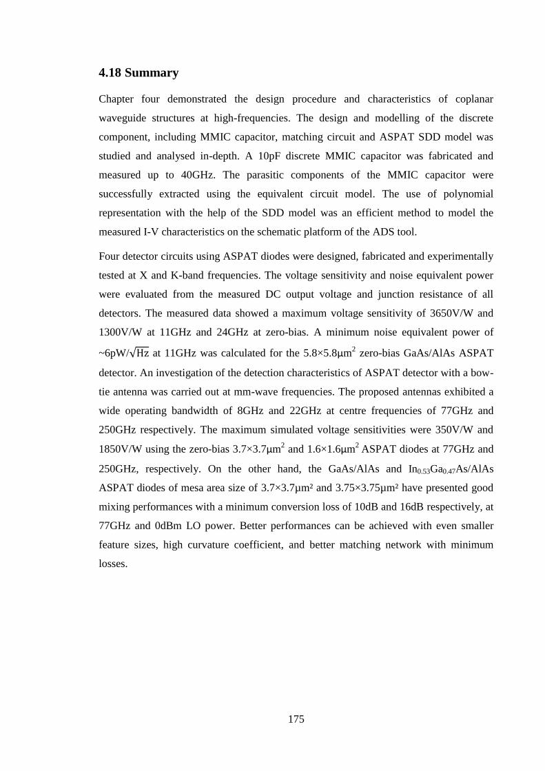
175
4.18 Summary
Chapter four demonstrated the design procedure and characteristics of coplanar
waveguide structures at high-frequencies. The design and modelling of the discrete
component, including MMIC capacitor, matching circuit and ASPAT SDD model was
studied and analysed in-depth. A 10pF discrete MMIC capacitor was fabricated and
measured up to 40GHz. The parasitic components of the MMIC capacitor were
successfully extracted using the equivalent circuit model. The use of polynomial
representation with the help of the SDD model was an efficient method to model the
measured I-V characteristics on the schematic platform of the ADS tool.
Four detector circuits using ASPAT diodes were designed, fabricated and experimentally
tested at X and K-band frequencies. The voltage sensitivity and noise equivalent power
were evaluated from the measured DC output voltage and junction resistance of all
detectors. The measured data showed a maximum voltage sensitivity of 3650V/W and
1300V/W at 11GHz and 24GHz at zero-bias. A minimum noise equivalent power of
~6pW/√Hz at 11GHz was calculated for the 5.8×5.8µm2 zero-bias GaAs/AlAs ASPAT
detector. An investigation of the detection characteristics of ASPAT detector with a bow-
tie antenna was carried out at mm-wave frequencies. The proposed antennas exhibited a
wide operating bandwidth of 8GHz and 22GHz at centre frequencies of 77GHz and
250GHz respectively. The maximum simulated voltage sensitivities were 350V/W and
1850V/W using the zero-bias 3.7×3.7µm2 and 1.6×1.6µm
2 ASPAT diodes at 77GHz and
250GHz, respectively. On the other hand, the GaAs/AlAs and In0.53Ga0.47As/AlAs
ASPAT diodes of mesa area size of 3.7×3.7µm² and 3.75×3.75µm² have presented good
mixing performances with a minimum conversion loss of 10dB and 16dB respectively, at
77GHz and 0dBm LO power. Better performances can be achieved with even smaller
feature sizes, high curvature coefficient, and better matching network with minimum
losses.

176
CHAPTER 5: PHYSICAL MODELLING AND
EXPERIMENTAL CHARACTERISATION OF APD
AND PIN PHOTODETECTORS FOR HIGH DATA
RATE APPLICATIONS
5.1 Introduction
The design, fabrication, and physical modelling of photodetector for the high-data-rate
optical application need full knowledge of electronic and optical characteristics of all
involved layers. Careful steps have to be followed to select proper materials in which
maximum performances can be obtained. Moreover, the thickness and doping of layers
are crucial in defining the electric field across the structure that, in turn, specifies the
transport mechanism of carriers. The work in this chapter deals firstly, standard
In0.53Ga0.47As/In0.52Al0.48As APD and In0.53Ga0.47As PIN photodetectors with different
light window aperture sizes were designed and then experimentally fabricated and
characterised regarding their DC and high-frequency optical characteristics. Secondly,
high-frequency equivalent circuits from fabricated devices were built up to 40GHz to
extract key diode parameters including (𝐶𝐽), (𝑅𝐽), and (𝑅𝑆) utilising the ADS tool.
Extracting the intrinsic parameters is necessary to calculate its cut-off frequency and
predict photodetectors performance for high-frequency applications. For the development
and fabrication of such high data-rate APD or PIN diode, it is more efficient to have a
physical model that can accurately predict and analyse the effect of different parameters
such as mesa area size, absorber layer thickness, and light window aperture size. This
model can help to adequately mitigate any performance degradation and lowering the
effective cost of production. This work concentrates on the optimisation of
photodetectors (PIN diode, and APD) in order to enhance their capability of operating at
data rates in excess of 25Gb/s. Using full virtual wafer fabrication physical modelling
(DC, AC, and optical characteristics), 3D analytical models were built and simulated for
both standard photodetectors using the ATLAS SILVACO tool. All simulations were
performed for normal incidence devices. The modelled structures are validated by the
fabricated devices in terms of electrical and optical characteristics. Three process factors,

177
namely: absorber thickness, light window aperture, and mesa area size were optimised to
enable the photodetectors to operate at a data rate higher than 25Gb/s. The optimised PIN
photodetector denoted as (15D) has an optoelectric 3-dB bandwidth of 35GHz at -5V
bias when a 10µW optical power is applied, while the optimised APD denoted as (15A)
and has an optoelectric bandwidth of 21GHz and a multiplication gain of 3 at -21.6V and
1µW incident optical power.
5.2 Epi-layer Structures of Photodetectors
The photodetector epi-layers were grown using Solid Source Molecular Beam Epitaxy
(SSMBE) on 620µm thick semi-insulating InP substrates. The standard PIN structures
(30S, 20S, and 15S) comprise of undoped InGaAs material as an absorber sandwiched
between two heavily doped ~0.1µm p-type In0.53Ga0.47As top and 0.5µm n-type
In0.53Ga0.47As bottom contact layers as depicted in table 5.1. The absorber is relatively
thick (~2µm), but this makes the PIN efficient at absorbing light in the (1.3 to 1.6µm)
wavelength region.
The standard APD structure (30A) as shown in table 5.2 comprises p-type In0.53Ga0.47As
top and n-type In0.53Ga0.47As bottom contacts, p-type In0.53Ga0.47As top and n-type
In0.52Al0.48As bottom cladding layers, undoped In0.53Ga0.47As absorber layer, p-type
In0.52Al0.22Ga0.25As grading layer, p-type In0.52Al0.48As charge sheet layer, and undoped
In0.52Al0.48As multiplication layer. The top and bottom contacts are heavily doped
~3x10¹⁹
cm-3
and ~1x10¹⁹
cm-3
with thicknesses of ~300nm and 500nm respectively.
TABLE 5. 1: EPI-LAYER STRUCTURE OF THE STANDARD In0.53Ga0.47As PIN
DIODE
Layer Material Doping (cm-3
) Thickness (µm)
Top Contact p+-In0.53Ga0.47As ~1x10¹⁹
~0.1
Absorber i-In0.53Ga0.47As Undoped ~2
Bottom Contact n+-In0.53Ga0.47As ~1x10¹⁹
~0.5
Substrate InP S.I. ~620

178
The highly doped contacts help to reduce the series resistance (𝑅𝑆) which leads to
improvements in the frequency response of the device. The absorber is relatively thick
(~1.2µm). The grading layer thickness is 50nm, which improves the frequency response
of the APD by reducing the band-discontinuity at the interface with the charge layer. The
charge layer has a doping profile of ~1x10¹⁸
cm-3
with a thickness of 50nm. The main
function of this layer is adjusting the electric field of the device. Finally, the
multiplication layer with a thickness of 200nm is buried under the charge layer.
5.3 Fabrication and Small Signal RF Equivalent Circuit Extraction
Figure 5.1 shows a fabricated photodetector employing a 50Ω coplanar waveguide
configuration for electrical and optical measurements. Three PIN photodetectors (15S,
20S, and 30S) were fabricated with a light window aperture size of 15, 20 and 30µm
respectively. The standard APD (30A) was fabricated with a light window aperture size
of 30µm. For the APD design, 𝐷𝑔𝑎𝑝 was designed to be ~13.5µm, while it was ~10µm
for the PIN structures. The width of the gold anode contact is 6µm. As a part of the high-
TABLE 5. 2: EPI-LAYER STRUCTURE OF THE STANDARD
In0.53Ga0.47As/In0.52Al0.48As APD (30A)
Layer Material Doping (cm-3
) Thickness (µm)
Top Contact p++-In0.53Ga0.47As ~3x10¹⁹
~0.03
Cladding p+-In0.53Ga0.47As ~1x10¹⁸
~0.17
Absorber i-In0.53Ga0.47As Undoped ~1.2
Grading p-Al0.22Ga0.25In0.52As ~5x10¹⁶
~0.05
Charge Sheet p+-Al0.48In0.52As ~1x10¹⁸
~0.04
Multiplication i-Al0.48In0.52As Undoped ~0.2
Cladding p+-Al0.48In0.52As ~2x10¹⁸
0.2
Bottom Contact n++- In0.53Ga0.47As ~1x10¹⁹
0.5
Substrate InP S.I. ~620

179
Figure 5.1: Fabricated photodetector. The inset shows the light window aperture (W) and 𝑫𝒈𝒂𝒑 of
the photodetector. (images are not to scale).
frequency characterisation, on-wafer (𝑆11) reflection parameter measurements were
performed for the open, short, and actual structures using an Anritsu VNA from 40MHz
to 40GHz at different bias. All measurements were performed in the dark at room
temperature. Advanced Design System (ADS) tool was employed to extract the intrinsic
and extrinsic component of the devices. The dimension of the GSG coplanar waveguide
was optimisedtogiveanimpedanceof50Ω. As there is no standard model for the APD
in ADS, an equivalent circuit model was built, and the fitting was made with the
measured data. The equivalent circuit of the open structure was built in ADS and is
represented by a capacitor only (𝐶𝑃), while the short structure is represented by an
inductor 𝐿𝑃. The simulated S-parameters of the equivalent circuits were fitted with the
measured ones to extract 𝐶𝑃 and 𝐿𝑃. The measured and simulated S-parameters
represented on a Smith chart for the open and short devices are shown in figure 5.2. The
simulated 𝑆11 data show excellent agreement with the measured data in the low-
frequency range up to 30GHz. At higher frequencies, there is a slight deviation between
the measured and simulated data of the short structure, which could be due to
measurement error or leakage issue. The extracted 𝐶𝑃 and 𝐿𝑃 of the standard APD (30A)
and PINs (30S, 20S, and15S) are 8 to10fF and 40 to 50pH respectively. The small
parasitic capacitance (𝐶𝑃) comes from the optimised coplanar waveguide design process.
The simulated 𝑆11 of the ADS equivalent circuits were fitted with the experimental
100µm 50µm
35µm
W
4µm
6µ
m

180
results to extract all parameters. Figure 5.3 depicts the measured and equivalent circuit S-
parameters of the PINs and APD photodetectors at fully depleted voltages.
Figure 5.2: Measured and simulated 𝑺𝟏𝟏 represented on smith charts of the open and short
structures and corresponding equivalent circuits.
Figure 5.3: Measured and simulated S-parameters represented on Smith charts and of the standard
PINs and APD at fully depleted bias.
Measured data
Simulated data
PIN (15S) PIN (20S)
PIN (30S) APD (30A)
Equivalent circuit at
negative bias voltage

181
Table 5.3 lists the extracted parameters of the APD and PIN diodes when fully depleted.
The fully depleted junction capacitance of the standard APD (30A) is 162fF while it was
found to be much smaller for the 15S, 20S, and 30S PIN diodes with extracted values of
46fF, 55.5fF, and 104fF respectively, and this is due to the larger light window aperture
size, mesa area size, and thinner depletion region of the APD.
Larger device capacitance degrades the high-frequency performance, as the RC and
transit time components limit the 3-dB optical bandwidth. The highly doped top and
bottom contacts resulted in a relatively small series resistance of the APD and PIN
diodes, which leads to improvements in the frequency response of the device when the
optimum intrinsic region width is employed. The extracted 𝑅𝑆 of the standard APD and
PIN diodes are10Ωand ~5Ωrespectively. The APD series resistance is larger due to the
extra resistances introduced from several layers. Above all, the separation between the
top and bottom electrodes is larger in the case of the APD structure (13.5µm vs 10µm),
which affects the total series resistance. The intrinsic cut off frequencies (𝑓𝑐𝑢𝑡−𝑜𝑓𝑓) were
evaluated for all structures using the usual expression (1/2𝜋𝑅𝑆𝐶𝐽) and found to be
692GHz, 478GHz, 255GHz, and 100GHz for the PIN (15S, 20S, and 30S), and APD
(30A) respectively. However, in the caseofa50Ωload the cut-off frequencies decrease
to 63GHz, 51.6GHz, and 27.3GHz for the PINs (15S, 20S, 30S) respectively, and 63GHz
TABLE 5. 3: STANDARD APD AND PIN DIODES EXTRACTED PARAMETERS
AT FULLY DEPLETED BIAS.
Component PIN (15S) PIN (20S) PIN (30S) APD (30A)
𝐶𝐽, fF 46 55.5 104 162
𝑅𝐽,kΩ 50 50 50 15
𝑅𝑆,Ω 5 5 5 10
𝐶𝑃, fF 10 10 10 8
𝐿𝑃 , pH 50 50 50 40
Intrinsic
𝒇𝒄𝒖𝒕−𝒐𝒇𝒇 (GHz)
692 478 255 100
Vertical lines are optional in tables. Statements that serve as captions for the entire table do not need
footnote letters. aGaussian units are the same as cg emu for magnetostatics; Mx = maxwell, G = gauss, Oe = oersted; Wb =
weber, V = volt, s = second, T = tesla, m = meter, A = ampere, J = joule, kg = kilogram, H = henry.

182
for the standard APD (30A). Extracting the junction capacitance of the devices using the
high-frequency small-signal equivalent circuit model is necessary to validate the
SILVACO physical model which exhibits almost the same value when the APD and PIN
diodes are fully depleted as will be discussed later.
5.4 Experimental Characterisation Tools
All devices were experimentally tested to obtain their electrical and optical
characteristics. The electrical characterisation was accomplished under dark room
condition and room temperature to measure the dark current, capacitance-voltage (C-V)
characteristic, and high-frequency S-parameter measurements up to 40GHz at different
bias. Different pieces of equipment were used in the work, including an RF probe station
and an Anritsu VNA to collect the S-parameter data.
For the optical characterisation, laser light of 1.55µm wavelength and variable power (1
to 100µW) was utilised to illuminate the device, as shown in the setup of figure 5.4. A
‘Lightwave Component Analyser’ (LCA) (HP 8703A) was employed to measure the 3-
dB bandwidth of the devices. The bias is applied using a DC supply (HP4142B)
connected to the Analyser through a bias-T.
Figure 5.4: Optical system set up on-wafer measurements.

183
5.5 Physical Modelling Characterisation Tool
The primary objective of the work was to build a quantitative and predictive physical
model for the standard 10Gb/s APD and 25Gb/s PIN photodetectors to validate the
measured electrical and optical characteristics. Numerical simulations of the standard
photodetectors under dark and light conditions and at room temperature were carried out
using the Atlas SILVACO tool. SILVACO [254] is a simulation software that allows the
user to build and model 2D and 3D structures electrically, thermally, or optically at
different bias, in effect performing a virtual wafer fabrication process. The simulator
considers many variables and conditions as the real device being simulated, and as a
result, the analysis process is more accurate, and the output results can be highly matched
to measured ones. The tool uses a set of differential equations such as Poisson’s and
drift-diffusion, as well as Fermi-Dirac or Boltzmann statistics to model carrier transport
through PIN or APD structures. As all equations are derived fromMaxwell’s laws, the
SILVACO Atlas tool is capable of performing DC, AC and transient analysis for 2D and
3D device structures on various material types (binary, ternary, and quaternary). The
process of building the structure, defining its parameters and variables, choosing the
desired model statement, performing the required analysis, and finally displaying the
results can be grouped into the following main statements:
Structure Specification: this statement is used to define the structure as follow:
•Mesh: Mesh statement is used to describe the structure either in two-dimensional (2D)
or three-dimensional (3D) Cartesian grids. All coordinates are in units of microns, and
the spacing parameter is used to improve the precision and accuracy of the analysis at a
given location.
•Region: This part defines the layers of the structure. Each layer represents a separated
section and needs to be defined in the statement independently. The mesh must be
assigned to a region, and the region number must be ordered from lowest to highest
region.
•Electrode: This statement defines the location of biasing points for the electrical and
optical analysis. In this study, two probes have been allocated as the anode and cathode.
The anode is allotted at the top of the vertical device while the cathode is at the bottom of
the structure.

184
• Doping: In this field, the doping concentration level for each region is defined
depending on the material type either p or n.
Material and Models Specification
•Material: Used to define the parameters of different materials of the device such as
energy band gap, effective mass, mobility, permittivity. By default, ATLAS has complete
parameters for Silicon, GaAs and AlAs materials. In the case of using a new material
(such as InGaAs or InAlGaAs), then all necessary parameters have to be specified and
manually defined in the material statement.
• Models: The most crucial part is the inclusion of the specific model for accurate
modelling of a particular device. Device structure and type determine the required
physical model, for instance, to model the impact ionisation process of the APD, an
IMPACT SELBER model is used as will be discussed later.
•Contact: Contact statement is used to specify the physical attributes of an electrode. An
electrode attached to the semiconductor material is assumed by default to be ohmic. If the
work function is defined, the electrode is treated as a Schottky contact.
Numerical Method Selection: This statement is used to compute the solution for
semiconductor device problems. The calculation is performed using a non-linear iteration
procedure that starts from an initial guess and uses an iterative process to find the
estimated solution.
Solution Specification: The user must define a log, solve, save statement in the ATLAS
simulation. These statements work together to provide data for analysis by other
functions. In this work, all three statements are used to analyse the I-V characteristics
produced by the device itself, its energy band diagram and different outputs. Problem
solution is turned on once the simulator runs at the solve statement. Later, in the log
statement, any DC, transient or AC data generated by the solve statement will be saved to
a file. Save statement used to store all data point to a node in the output file.
As the SILVACO library does not contain material parameters for InGaAs, InAlAs, and
InAlGaAs, all III-V material parameters were obtained both from the works of literature
and from validation from many devices studied over the years in our laboratory [55, 139,
255-257].

185
5.6 Physical Modelling and Optimisation Details
The photodetectors were designed and fabricated with a circular mesa shape having a
specific light window aperture size. A 3D modelling was carried out to simulate the
performance of photodetectors. The 3D simulation is more accurate than the 2D one, as it
models the exact structure dimensions which take into account the effect of the electric
field at the edges of the structures. However, for simplicity, the photodetectors were built
and modelled with a 3D-rectangular mesa shape, as shown in figure 5.5. The rectangular
shape photodetectors have precisely the same dimensions of the fabricated ones. In
Silvaco, the 3D-rectangular coordinates are represented by X-Z-Y. The effective mesa
area sizes are 1962µm², 1256µm², and 961µm² for the standard PIN (30S), PIN (20S),
and PIN (15S) diodes respectively and 1960µm² for the APD (30A). Following this, the
length (𝐿𝑚𝑒𝑠𝑎) and width (𝑊𝑚𝑒𝑠𝑎) of the mesa were calculated for all structures. The
same calculations were performed for all other dimensions (light window aperture size,
𝐷𝑔𝑎𝑝, anode and contact sizes) of the standard and optimised photodetectors.
Figure 5.5: Modelled 3D rectangular photodetector.

186
The experimental characterisations of the APD (30A) and PIN diodes (30S, 20S, and
15S) were accomplished to investigate their electrical and optical performances
realistically. The electrical characteristics were measured in the dark and at room
temperature. Capacitance-Voltage (C-V) measurement are crucial to validate the
extracted 𝐶𝐽 from the 𝑆11 reflection data and to practically extract the punch-through
voltage of the APD as well as ensuring that the actual doping profile and thickness of the
layers are close enough to the designed ones. This work firstly uses numerical
simulations as a tool to build a 3D quantitative and predictive physical model for the
APD and PIN photodetectors and to validate the measured electrical and optical data.
Secondly, the successful and verified models were then adopted to virtually investigate
the effect of different parameters and optimise the performances of the photodetectors.
The APD structure requires more care to build and activate the appropriate models since
it is more complicated compared to the PIN diode. Shockley-Read-Hall (SRH) model
and Fermi-Dirac statistics were used to model the generation-recombination and carrier
drift-diffusion processes. To model the impact ionisation process of the APD, an
IMPACT SELBER model was used. The model was developed by Selberherr [147] to
estimate the impact ionisation rate coefficients 𝛼(𝐸) and 𝛽(𝐸). The model was derived
using the classical Chynoweth model [258] and based on the equations 2.32 and 2.33
which include the parameters (AN, BN, BETAN, AP, BP, BETAP) provided in chapter 2.
SELBER model calculates 𝛼(𝐸) and 𝛽(𝐸) by computing the value of the lattice
temperature-dependent parameters (AN, BN, AP, BP) using the equations reported in
[259]. BETAN and BETAP were predicted by Shockley in [260] with a value equal to ~1.
The optimisation of our structures consists of two process factors which have a
significant effect on the high-frequency performances. The absorber thickness was
selectively thinned to be 0.5µm for the APD and PIN diode with the aim of reducing the
transit time of the electrons and thus enhancing the 3-dB optoelectric bandwidth.
However, a thinner depletion region results in a higher junction capacitance. So, further
optimisation was carried out by reducing the mesa area size, top gold electrode width,
and the light window aperture. The latter was optimised to be 15µm, making the effective
mesa area of both photodetectors ~490µm². A smaller window aperture would increase
the complexity of the packaging and assembly of the devices. The design process of the
absorber layer determines the responsivity and the maximum operating 3-dB bandwidth

187
of the photodetector. For investigation purposes, 𝐹𝑇, 𝐹𝑅𝐶, and 𝐹3𝑑𝐵 were calculated and
plotted in figure 5.6 for the optimised APD as a function of the intrinsic region width.
0.4 0.6 0.8 1.0 1.2 1.410
20
30
40
50
60
70
Ban
dw
idth
(G
Hz)
Intrinsic Region (m)
FT
FRC
Total F3dB
Figure 5.6: Calculated 3-dB optical bandwidth of the optimised In0.53Ga0.47As/ In0.52Al0.48As APD.
It is noteworthy to mention that the optimised APD and PIN diode are denoted as (15A)
and (15D), respectively. Table 5.4 summarises the devices reported in this thesis. The
intrinsic region is assumed to be fully depleted, which is the case when the bias is equal
to -15V. Therefore, the plot in figure 5.6 is restricted to (-15V<bias<90%𝑉𝐵𝑅 (breakdown
voltage)), with an internal gain of higher than 1.
TABLE 5. 4: THE STANDARD AND OPTIMISED DEVICES
Standard Optimised
APD PIN APD PIN
Device 30A 15S 20S 30S 15A 15D
188
At bias higher than (90%𝑉𝐵𝑅), the saturated drift velocity of carriers starts to decrease
due to electron scatteringfromГtoLandXvalleysathighelectricfieldscausingitto
degrade the 3-dB optical bandwidth as will be discussed later. The intrinsic region of the
optimised APD (15A) includes both a 0.5µm absorber layer and a 0.2µm multiplication
layer. Figure 5.6 indicates that the carrier transit frequency dominates the 3-dB optical
bandwidth for an intrinsic region thickness greater than 1µm. On the contrary, it is
limited by the RC bandwidth for an intrinsic region thickness smaller than 0.5µm. The
highest calculated 𝐹3𝑑𝐵 of the optimised APD (15A) structure is 22.5GHz when the
intrinsic region width ranges between 0.5 to 0.8µm meaning that the optimum absorber
thickness is probably around 0.5µm. However, these calculated results do not take the
effect of the parasitic elements into account which can have a large impact at high
operating frequencies.
5.7 Dark Currents and C-V Characteristics
The dark currents of standard APD (30A) and PIN diodes (15S, 30S, and 20S) were
measured up to -25V and -5V bias respectively using a probe station under dark and at
room temperature conditions.
The modelling process started with simulating I-V and C-V characteristics by
maintaining a good agreement with experimental data, to build appropriate physical
models and validate material parameters used which then can be used to simulate and
predict the optical characteristics of higher frequency photodetectors. The inclusion of
different models is necessary to simulate the exact physical phenomena. IMPACT
SLEBER was used to model the impact ionisation process of the APD that causes the
avalanche breakdown phenomena at high internal gains. Such a phenomenon is quite
challenging to model as it depends on several material parameters such as carrier’s
impact ionisation coefficient, applied electric field and doping profiles. The modelling
process of the APD was performed using two conditions. The first condition was based
on the dark current characterisation, where no electron-hole generation is defined in the
absorber layer, and no multiplied photocurrent is created. The output current is a sum of
the un-multiplied and multiplied dark current. Therefore, electrons travel with their
average velocity in both multiplication and charge sheet layers. The electron velocity was
set to 2.5x10⁶
cm/s and 1x10⁷
cm/s in the charge and multiplication layers, respectively.

189
The electron velocity in the absorption layer was set to ~1.5x10⁷
cm/s. The electron
mobility of each layer (InGaAs, InAlAs and InAlGaAs) are different depending upon the
doping profile of each layer. All required values were obtained from the literature in
[255-257]. The key fitting parameters used in SILVACO modelling are shown in table
5.5. It is noteworthy to state that ATLAS SILVACO tool assumes a constant effective
mass, which does not accurately reflect the impact ionisation process of APD structures.
The band-to-band tunnelling current was not considered due to the inclusion of the
graded and charge sheet layers which provide enough electric field separation between
the absorber and multiplication layers. Band-to-band tunnelling current starts to dominate
the dark current of the APD when the multiplication region is smaller than 100nm [261].
TABLE 5. 5: KEY FITTING PARAMETERS USED IN SILVACO PHYSICAL
MODELLING.
Parameter Absorber layer
(In0.53Ga0.47As)
Multiplication layer
(In0.52Al0.48As)
Grading layer
(In0.52Al0.22Ga0.25As)
Electron mobility
(v/cm²) 11000 4500 2300
Energy gap (eV) 0.75 1.44 ~0.99
Affinity (eV) ~4.5 ~4.25 ~4.38
Permittivity 13.9 12.2 ~12.5
Electron carrier life
time (ns) 100 - -
Electron effective
mass ~0.042 ~0.085 ~0.06
Hole effective mass ~0.46 ~0.6 ~0.61

190
The most important phenomena to take into account for accurate physical simulation of
the dark current is the impact ionisation process, which is described by the following
equation [254]:
𝐺= 𝛼(𝐸) |𝐽|𝑛 + 𝛽(𝐸) |𝐽|𝑝 (5.1)
where (𝐺) is the generation rate of the electron-hole pairs, |𝐽|𝑛 and |𝐽|𝑝 are the electron
and hole current densities. In SILVACO, parallel electric field dependence (FLDMOB)
and a local field IMPACT SELBER models were used to model the lateral electric field
mobility dependency and impact ionisation rate of electron and hole of APD structure.
Both models are necessary to fit the dark current and break down voltage (𝑉𝐵𝑅). Through
the simulation, SILVACO calculates impact ionisation parameters (AN, BN, BETAN, AP,
BP, BETAP) according to the material parameters of the charge sheet multiplication
regions (lattice temperature and energy gap) as well as the required model for the impact
ionisation process. The calculation process of the parameters can be found in details in
[254]. The output window of the SILVACO resulted in values of 8.6x10⁶
cm-1
, 2.3x10⁷
cm-1
, 3.5x10⁶
cm-1
, and 4.5x10⁶
cm-1
for AN, AP, BN and BP respectively and 1 for both
BETAN and BETAP respectively. The black and red lines in figure 5.7 (a) and (b) which
represent the simulated and measured dark currents of the standard APD (30A) and PIN
diode (15S) are very close to each other.
The measured dark currents of the standard APD (30A) and PIN diode (15S) are ~8nA
and 2.2nA at 90%𝑉𝐵𝑅 and -5V bias, respectively. The doping profile of the charge sheet
layer plays an important role in determining the breakdown voltage of the APD.
Therefore, the doping was changed slightly to keep 𝑉𝐵𝑅 at (-23.7V) for the standard and
optimised APD. The doping profile of the charge sheet layer was set to ~6.5x10¹⁷
cm-3
.
Dark current is directly proportional to device mesa size; therefore, scaling of the device
reduced the dark current of both photodetectors. The optimised APD (15A) exhibits a
dark current of 1.5nA at 90%𝑉𝐵𝑅 which is much lower than the InGaAs and Si-Ge APD
reported in [131, 138, 262]. The electric field of our APD is greatly confined in the
InAlAs multiplication layer, and only the Shockley-Read-Hall process occurs in the
InGaAs absorber layer and generates the dark current. Similarly, the optimised PIN diode
(15D) has a dark current of <2nA at -5V bias which is comparable to previously reported
Ge and InGaAs PIN diodes in [155, 263].

191
-25 -20 -15 -10 -5 010
-13
10-12
10-11
10-10
10-9
10-8
10-7
10-6
10-5
10-4
10-3
-5 -4 -3 -2 -1 010
-11
10-10
10-9
10-8
10-7
10-6
(b)
Cu
rren
t (A
)
Voltage (V)
Measured standard APD (30A)
Simulated standard APD (30A)
Simulated optimised (smaller) APD (15A)
(a)
VBR
=-23.7V
Cu
rren
t (A
)
Voltage (V)
Measured standard PIN diode (15S)
Simulated standard PIN diode (15S)
Simulated optimised (smaller) PIN diode (15D)
Figure 5.7: Measured and simulated dark currents of the standard and optimised
(a): In0.53Ga0.47As/In0.52Al0.48As APDs, and (b): In0.53Ga0.47As PIN photodetectors.

192
The standard PIN diodes (20S) and (30S) have recorded a minimum dark current of
2.9nA and 3.7nA at -5V bias, respectively. These values make the devices appropriate
candidates to achieve high SNR and high sensitivity in optical communication receivers.
The total measured capacitances including the junction capacitance and pad capacitance
were extracted from the measured S-parameter at different bias using the well-known
expression (𝐼𝑚𝑎𝑔(𝑌11)/2𝜋𝑓). The SILVACO models were used to simulate and fit the
junction capacitances of the standard APD (30A) and PIN diode (15S) with the
experimental data, as well as simulating the C-V data of the optimised (smaller and
thinner) structures (15A and 15D) as depicted in figure 5.8. The plot shows an excellent
fit between the measured and simulated data for the standard APD (30A) and PIN diodes
(15S). The fully depleted capacitance occurs at a bias (>-15V and >-3V) for the APDs
and PIN diodes respectively. The slope indicates that the punch-through voltage (𝑉𝑃𝑇) of
the APD is (-12.5V), which is far enough from the 𝑉𝐵𝑅 of (-23.7V). It is clear that
minimising the light window aperture and the mesa area size of the APD has resulted in a
remarkable improvement in the fully depleted junction capacitance of the optimised APD
(15A). However, this is not the case for the optimised PIN diode (15D), where reducing
the mesa area size was not sufficient enough to compensate for the increase of the
junction capacitance value due to thinning of the absorber thickness. Such an APD and
PIN diode with junction capacitances of 72fF and 106fF respectively and relatively small
series resistances should be suitable candidates for data rate applications higher than 25
Gb/s. The total variation of the breakdown voltage with the temperature was calculated
for the standard and optimised APDs.
The findings show that the breakdown voltage of the optimised APD (15A) is less
sensitive to the ambient temperature compared to the standard design (30A) (14.21mV/K
vs 24.36mV/K).

193
-21 -18 -15 -12 -9 -6 -3 00
50
100
150
200
250
300
-10 -8 -6 -4 -2 00
50
100
150
200
250
Ju
ncti
on
Ca
pa
cit
an
ce (
fF)
Voltage (V)
Measured standard APD (30A)
Simulated standard APD (30A)
Simulated optimised (smaller) APD (15A)
VPT
=-12.5V
(b)
Measured standard PIN diode (15S)
Simulated standard PIN diode (15S)
Simulated optimised (smaller) PIN diode (15D)
Ju
ncti
on
Ca
pa
cit
an
ce (
fF)
Voltage (V)
(a)
Figure 5.8: Measured and simulated dark junction capacitance versus bias of the standard and
optimised (a): In0.53Ga0.47As/In0.52Al0.48As APDs, and (b): In0.53Ga0.47As PIN photodetectors.

194
5.8 Optical and Noise Characteristics
The photocurrents of the conventional devices were measured using a 1.55µm laser light.
The incident optical powers on the APD and PIN diodes were -30dBm and -20dBm
respectively. APD and PIN diode models were optically characterised by taking into
account the generation process of the electron-hole pair in the absorber layer.
In SILVACO, different parameters have to be considered to calculate the photocurrent
such as material quantum efficiency, material absorption coefficient, and the effect of
absorption losses and transmission and reflection factors [254]. The optical-generation
rate is calculated in SILVACO using the formula [254]:
𝑂 − 𝐺= Ƞ × 𝑃∗ 𝜆
ℎ 𝑐 × 𝛼(𝜆) × 𝑒−𝛼(𝜆)𝑦 (5.2)
where Ƞ is the quantum efficiency, 𝑃∗ represents the effect of absorption losses, and
transmission and reflection factors, 𝑐 is the speed of light, 𝑦 is the optical penetration
depth. Laser light was utilised of a wavelength of 1.55µm to generate electron-hole pairs
in the absorption layer. The laser power was 1µW. In the photocurrent simulation
process, the same models (SRH, Fermi-Dirac statistics, IMPACT SELBER, and
FLDMOB) and fitting parameters of the dark current and C-V characteristics were used
except that the electron velocity in the absorption and charge sheet layers were set to
2x10⁷
cm/s and 5x10⁷
cm/s respectively as the electric field is higher under light
conditions. In [139], a Monte Carlo model was used to simulate the optical
characteristics of the APD. In [9], it was shown that in thin multiplication regions and
high electric fields, the electron could travel with a speed that is much higher than its
saturation velocity. This was also confirmed in [167], where the carrier velocity used in
the model was much higher than the saturation velocity for an APD with a 200nm
InAlAs multiplication region. This concept was further explored in our model, where the
charge sheet and Multiplication layers have a high electric field profile, as shown in
figure 5.9. The electric field of the optimised APD is close to ~600kV/cm compared with
a ~700kV/cm for the standard APD design, furthermore, reducing the absorber thickness
of the APD by ~60% led to an increase in the electric field of the absorber layer by
194%. A high electric field affects the drift saturation velocity of the carries and degrades
the carrier transit frequency. So, care has to be taken to choose the optimum absorber
thickness.

195
0.0 0.3 0.6 0.9 1.2 1.5 1.8 2.1 2.40
100
200
300
400
500
600
700
800
Ele
ctr
ic F
ield
(K
V/c
m)
Thickness (mm)
Standard APD (30A)
Optimised APD (15A)
Figure 5.9: Simulated electric field distribution of the In0.53Ga0.47As/In0.52Al0.48As standard and
optimised APDs under -20V bias.
The physical models are in excellent agreement with the fabricated devices, as is seen in
the black and red lines of figure 5.10 (a) and (b). The optimised APD (15A) has virtually
a flat photocurrent between 𝑉𝑃𝑇 and 𝑉𝐵𝑅 which results in a practically constant internal
gain. At 𝑉𝐵𝑅, the photocurrent raises significantly due to the occurrence of a large
number of impact ionisation events resulting in a high internal gain. The extracted 𝑉𝐵𝑅
and 𝑉𝑃𝑇 from the photocurrent data agree well with the values from dark current and C-V
data. The measured DC responsivity without anti-reflection (AR) coating layer is 9A/W
at 90%𝑉𝐵𝑅 bias for the standard APD (30A). On the other hand, the measured dc
responsivities of the standard PIN diodes (15S, 20S, and 30S) were 0.67A/W, 0.73A/W,
and 0.76A/W respectively at -5V bias. The optimised APD (15A) photocurrent is ~1.4µA
at 90%𝑉𝐵𝑅 corresponding to a multiplied DC responsivity of 1.4A/W.

196
-25 -20 -15 -10 -5 010
-11
10-10
10-9
10-8
10-7
10-6
10-5
10-4
10-3
-5 -4 -3 -2 -1 010
-6
10-5
Cu
rren
t (A
)
Voltage (V)
Measured standard APD (30A)
Simulated standard APD (30A)
Simulated optimised (smaller) APD (15A)
Measured standard PIN diode (15S)
Simulated standard PIN diode (15S)
Simulated optimised (smaller) PIN diode (15D)
Cu
rren
t (A
)
Voltage (V)
(a)
(b)
VBR
=-23.7V
VPT
=-12.5V
Figure 5.10: Measured and simulated photocurrents of the standard and optimised (a):
In0.53Ga0.47As/In0.52Al0.48As APDs, and (b): In0.53Ga0.47As PIN diodes.

197
The optimised APD could not maintain a high responsivity as a result of its thinner
absorber thickness. On the other hand, the optimised PIN diode (15D) has a photocurrent
of 4.6µA while offering a DC responsivity of 0.46A/W at -5V bias. At the same absorber
thickness and incident optical power, the APD provides higher responsivity compared to
the PIN diode due to the multiplication process of the photocurrent. The internal gain (𝑀)
was calculated for the standard and optimised APDs (30A and 15A), as shown in figure
5.11.
-24 -21 -18 -15 -120
10
20
30
40
50
60 Measured gain of standard APD (30A)
Simulated gain of standard APD (30A)
Simulated gain of optimised APD (15A)
F(M) of standard APD (30A)
F(M) of optimised APD (15A)
Voltage (V)
Inte
rn
al
Ga
in (
M)
0
1
2
3
4
5
6
7
F(M
)
Figure 5.11: Measured and simulated internal gain and excess noise factor of the standard and
optimised In0.53Ga0.47As/In0.52Al0.48As APDs.
The low internal gain of ~3 at 90%𝑉𝐵𝑅 of the optimised APD is mainly caused by the
decrease of the electric field in the multiplication layer. Under a uniform electric field,
the excess noise factor 𝐹(𝑀) as a function of the applied bias was estimated and plotted
in figure 5.11.
The low internal gain introduced less excess noise of ~2.2 for the optimised APD (15A)
at 90%𝑉𝐵𝑅 bias, and 𝑀=~3, which is comparable to the value reported in [136, 264, 265].
Less excess noise is highly essential to achieve high SNR values. The photodetector noise
is another figure of merit which determines the maximum achievable SNR and data-rate.

198
The total noises of the standard and optimised photodetectors were theoretically
calculated at 1Hz, as shown in table 5.6.
The noise characteristics are estimated at a bias of 90%𝑉𝐵𝑅 and -5V for the standard and
optimised APD and PIN diode respectively. In the case of a PIN diode, it is clear that the
noise of standard and optimised PIN diodes (15S and 15D) is dominated by the thermal
noise caused by the equivalent resistances of (𝑅𝑆+𝑅𝐿). The existence of internal gain (𝑀)
resulted in a high shot noise of ~37pA/√Hz for the standard APD (30A). However, this
was reduced to ~2.8pA/√Hz for the optimised APD (15A) since 𝑀 was decreased to 3.
𝑆21 represents the optoelectric response and is given by the ratio of photocurrent to the
optical power in dB unit. 𝑆21 response of the APD and PIN photodetectors were
simulated using the standard and optimised SILVACO models and then compared with
the measured ones. Figure 5.12 depicts the normalised measured and simulated
frequency photo-response of the standard and optimised APDs (30A, and 15A), and PIN
diodes (15S, 15D) at 90%𝑉𝐵𝑅 and -5V bias respectively. The 𝑆21 response of PIN diode
was shifted by -20dB in order to separate it from the APD response. The measured 3-dB
TABLE 5. 6: NOISE CHARACTERISTICS OF THE STANDARD AND OPTIMISED
APDS AND PIN DIODES AT 90%𝑉𝐵𝑅 BIAS
Parameter Standard
APD (30A)
Optimised
APD (15A)
Standard
PIN (15S)
Optimised
PIN (15D)
ID, nA 11 0.5 2 1.5
Iph, µA 9 1.4 6.7 4
Req, Ω 60 60 55 55
F(M) ~6 ~2.2 Free Free
Shot noise, pA/√Hz ~37 ~2.8 ~1.46 ~1.1
Thermal noise,
(pA/√Hz)
~16.5 ~16.6 ~17.3 ~17.3
Net noise, pA/√Hz ~53.5 ~19.3 ~18.76 ~18.4

199
optoelectric bandwidth of the standard APD (30A) and PIN diode (15S) is 6.7GHz and
20GHz, which agrees well with simulated ones. The maximum optoelectric bandwidth of
the optimised PIN diode (15D) is 35GHz which is comparable to the reported value in
[155], though the light window aperture is 3 times smaller than in our design.
0 10 20 30 40-30
-20
-10
0
@ -5V
@ 90%VBR
B.W=35GHz
No
rm
ali
sed
S21
Frequency (GHz)
B.W=21GHz
Figure 5.12: Normalized 𝑺𝟐𝟏 response of the In0.53Ga0.47As/In0.52Al0.48As APD and In0.53Ga0.47As PIN
diode, (red and black are the measured and simulated standard APD (30A), blue is the simulated
optimised APD (15A), green and brown lines refer to the measured and simulated standard PIN
diode (15S), and purple is the simulated optimised PIN diode (15D)).
The simulated optoelectric bandwidth of the optimised APD (15A) is 21GHz and agrees
well with the theoretically calculated one of 22.5GHz when the intrinsic region width is
0.7µm (0.5µm absorber layer, and 0.2µm multiplication layer). The standard and
optimised APDs provide a gain-bandwidth product of ~220GHz and ~63GHz at 90%𝑉𝐵𝑅
bias. The simulation process has shown that the bandwidth of the optimised APD (15A)
decreased to ~14GHz when the applied bias reached -22V, as shown in figure 5.13.

200
-18 -19 -20 -21 -220
5
10
15
20
25
Measured standard APD (30A)
Simulated standard APD (30A)
Simulated optimised (smaller) APD (15A)
3-d
B B
an
dw
idth
(G
Hz)
Voltage (V)
Figure 5.13: Measured and simulated 3-dB Bandwidth versus bias of the standard and optimised
In0.53Ga0.47As/In0.52Al0.48As APDs.
This is mainly due to electron scattering from ГtoLandXvalleysathighelectricfields.
As a result, electrons have higher effective mass and, thus, lower drift velocity. The
fitting parameter (charge sheet layer electron velocity) was changed according to the gain
values because of the field-velocity dependency. The electron velocity of charge sheet
layer was adjusted to fit the simulated 3-dB bandwidth with the measured one at different
bias according to the velocity overshot in the thin multiplication layer. For a gain of 5 to
10, the electron velocity in the absorption layer, and the multiplication layer were set to
2x10⁷
cm/s, and 1x10⁷
cm/s respectively. The effect of the velocity overshoot was applied
on the electron velocity in the charge sheet layer. Therefore the electron velocity of the
charge sheet layer was varied according to the applied bias, and was set to 9×10⁶,
4.4×10⁶, 2.5×10
7, 2.5×10
6, and 5.25×10
5 cm/s at -18, -19, -20, -21, and -22V bias
respectively. The 3-dB bandwidth of the standard PIN diodes (20S and 30S) were also
experimentally measured and found to be 17GHz and 14.5GHz respectively at -5V bias
which makes them suitable candidates for applications with data rate exceeding 18Gb/s.

201
5.9 Reported PIN Photodetectors
To date, various techniques and structures have been investigated to develop reliable and
stable PIN photodetectors over optical fibre links with data rates exceeding 50Gbit/s.
Table 5.7 summarises some of the reported PIN photodetectors using different absorber
materials and thicknesses. Much attention has been paid to realise a high data rate PIN
photodetectors based on InGaAs and germanium absorber due to their improved
performances compared to other materials. The thick InGaAs PIN diodes reported in
[160, 266] have shown very small dark currents and high responsivity of 0.05nA and
~1A/W at 1.55µm wavelength, respectively. As a comparison at the same absorber
thickness of 4µm, the InGaAs diode in [129] demonstrated a very small dark current of
10nA compared to 195nA for the germanium one reported in [39]. Besides that, the
InGaAs PIN photodetector exhibited higher responsivity (0.9A/W vs 0.6A/W) at 1.55µm
wavelength, and larger 3-dB bandwidth (18GHz vs 13.5GHz), although, it was fabricated
with a larger mesa area size (55µm vs 40µm). The reason is mainly due to the higher
quantum efficiency and higher carrier velocity of the InGaAs material.
A large 3-dB bandwidth PIN photodetector (39GHz) based on germanium material was
reported in [155]. The diode structure consisted of 0.307µm of germanium absorber and
was fabricated with a 10µm diameter size. The photodetector was designed and realised
with two mesa structure shaped to mitigate the effect of parasitic capacitance. Such a PIN
photodetector with a dark current of >75nA at -2V bias is not a suitable candidate for
high sensitivity receivers. Furthermore, the small diameter size (10µm) could result in in-
flexible alignment tolerance with the fibre optic. The work did not report the measured
responsivity which is believed to be very low as a result of the very narrow absorber
layer and more importantly the low quantum efficiency of germanium at the 1.55µm
wavelength. Another PIN photodetector made of 0.33µm germanium absorber was
reported in [267]. The device recorded a very wide-bandwidth of 49GHz at -2V bias and
1.55µm. Again, due to the relatively thin absorber layer, the device was found to have a
high leakage current and very low responsivity of ~1.9µA and 0.05A/W respectively.
Low responsivity limits the use of PIN diode in high sensitivity receivers. The device
developed in [263] was made of a 1µm-InGaAs absorber and grown on a semi-insulating
Si substrate. The photodetector recorded the smallest dark current for Si-InGaAs bonded
wafer. However, the photodetector suffers from a high seriesresistanceof40Ω due to the

202
high resistivity of the substrate. Finally, the table also shows the main achievements of
the standard and optimised PIN photodetectors, which have a very small dark current of
1.7nA and 1.4nA at -2V bias respectively, as well as wide 3-dB bandwidth compared to
the reported works, based InGaAs and germanium materials.

203
TABLE 5. 7: KEY REPORTED PIN PHOTODETECTOR PERFORMANCES
Structure Diameter
(µm)
Absorber Ɍ𝑷𝑰𝑵 (A/W) 𝑰𝒅𝒂𝒓𝒌−𝑷𝑰𝑵 (nA) 𝑭𝟑𝒅𝑩 (GHz) Ref.
Material Thickness (µm)
Circular Mesa 70 Undoped-
InGaAs 1.8 0.9@λ=1.4µm ~5 @ -2V 4 [153]
Circular Mesa 50 Undoped-
InGaAs 2 ~1@λ=1.55µm 0.01 @-2V 7.1 [160]
Circular Mesa 90 Undoped-Ge 4 0.9@λ=1.55µm ~1000 @ -2V 7.5 [39]
Circular Mesa 50 Undoped-
InGaAs 2.5 1@λ=1.55µm 0.04 @ -2V 10.3 [266]
Circular Mesa 40 Undoped-Ge 4 ~0.6@λ=1.55µm 195 @ -2V 13.5 [39]
Circular Mesa 35 Undoped-
InGaAs 1.5 ~1 @λ=1.55µm N/A 17 [268]
Circular Mesa 55 Undoped-
InGaAs 4 0.9@λ=1.55µm ~10 @ -2V ~18 [129]
Circular Mesa 30 Undoped-
InGaAs 1 N/A 0.1 @ -2V 21 [263]
Circular Mesa 20 Undoped-Ge 0.7 0.3@λ=1.55µm ~600 23.3 [41]
Circular Mesa 10 Undoped-Ge 0.307 N/A >75 39 [155]
Circular Mesa 10 Undoped-Ge 0.33 0.05@λ=1.55µm 1900 at -2V 49 [267]
Circular Mesa
(15S) 35
Undoped-
InGaAs 2 0.7@λ=1.55µm 1.7 at -2V 20 This work
Circular Mesa
(15D) 25
Undoped-
InGaAs 0.5 0.46@λ=1.55µm 1.4 at -2V 35 This work

204
5.10 Reported APDs
In the same manner, many groups have focused on optimising the dynamic functions of
APDs with the aim of increasing the gain-bandwidth product and maintaining low
leakage current for high-sensitivity receivers. Table 5.8 lists most of the reported APD
works for 1.33 to 1.55µm wavelength applications. Significant works have been
presented in the literature showing the performances of high data-rate APDs for long-
distance photo-detection over fibre optics [170]. Si and Ge materials were employed to
detect light wavelengths of 1.3µm [37, 38, 157, 265, 269] and 1.55µm [37, 40]. Si
material is well-known for its low 𝑘𝑟𝑎𝑡𝑖𝑜 which is the key for low exess noise and high
gain-bandwidth APD. Simple epi-layer structures were demonstrated in [265, 269]
including a low-doped Si charge layer sitting between two intrinsic 1µm-Ge-absoption
and 0.5µm-Si-multiplication layers. The APDs have a circular mesa shape with a
diameter of 30µm which resulted in a fully depleted capacitance of 77fF in the case of
[265]. The photodetectors recorded a maximum gain-bandwidth product of 340GHz and
840GHz at a light wavelength of 1.31µm. However, they have low sensitivity, low
responsivity (~0.55A/W) and large dark current (~1µA) resulting from the narrow band
gap of Ge (0.6eV) and the low absorption coefficient/quantum efficiency at longer
wavelengths. Huang et al. [37] reported a 10Gb/s and 25Gb/s Si-Ge APDs in which the
absorption layer thickness was 0.6µm. For the 10Gb/s design, a tensile strain Ge absorber
with an improved absorption coefficient was utilised to improve the responsivity at
1.55µm wavelength. The device recorded the highest measured responsivity of 0.9A/W
at unity gain. The large mesa area size of 35µm and short absorber limit the 3-dB
bandwidth to ~7GHz and also led to the introduction of a large dark current of 3000nA at
0.9𝑉𝐵𝑅. The 25Gb/s Si-Ge APD was realized by reducing the mesa area size to 20µm
which also allow reducing the dark current to ~800nA at 90%𝑉𝐵𝑅 bias. However, the
large dark current limits the receiver sensitivity to -23.5dBm at 10−12 bit error rate.
The waveguide Si-Ge APD structure was also proposed in [131] with a maximum
sensitivity of -16dBm and -25dBm at 25Gb/s and 12.5Gb/s data rate respectively. The
device is capable of achieving a maximum gain-bandwidth product of 276GHz at a gain
of ~12. However, the use of a p-doped Ge absorber layer resulted in a large dark current
of ~400nA at 90%𝑉𝐵𝑅 bias. Despite the great efforts performed to enhance the Si-Ge

205
APDs, they are still not the prefered candidates to be integrated in >25Gb/s receivers due
to the limitations mentioned above.
The InGaAs/InAlAs APDs has gained much attraction for 1.33 to 1.55µm wavelength
applications. For 10Gb/s data rate applications, a basic design of single circular mesa
shape and thick undoped absorber layer APDs were reported in [55, 270-272]. The use of
mesa diameter size of ~30µm and free doped thick InGaAs absorber (1 to1.3µm) in [55,
271, 272] resulted in having a small dark current of <23nA at 90%𝑉𝐵𝑅. Moreover, the use
of thinner InAlAs multiplication layer in [272] maximised the GBP to 240GHz compared
to 140GHz in [271]. The maximum reported GBP (480GHz) was reported in [273]. The
Al0.85Ga0.15As0.56Sb0.44 material served as the multiplication layer. This material has the
smallest temperature coefficient of breakdown voltage (𝜌𝑚=0.86 to 0.9mV/K) for a
0.11µm-thick [274, 275]. Another advantage is the small 𝑘𝑟𝑎𝑡𝑖𝑜=0.08 to 0.1 which is
highly preferred for high-gain and low excess noise factor APDs. However, the very thin
absorber layer in [273] exhibited a high dark current of >1000nA which limits the
maximum sensitivity of the receiver for high data rate applications. To reduce the dark
current below 1nA, a graded p-doped InGaAs absorber APD was introduced in [276].
The small dark current and large 3dB-bandwidth makes the photodetector suitable
enough for 25Gb/s receivers. For 25Gb/s receivers, APDs having three mesas
configuration and a hybrid InGaAs absorber were demonstrated in [137, 169-172, 262,
277-279]. The triple mesas design was used to confine the electric field inside the
multiplication regions while minimising it at the sidewall of photodetector. The hybrid
absorber is composed of un-doped and p-doped InGaAs materials to maximise the
bandwidth without degrading the responsivity. Moreover, the InAlAs multiplication layer
was reduced to ~0.1µm to shorten the avalanche delay time. Though, a high dark current
of 200 to 1000nA was measured at 90%𝑉𝐵𝑅. In [170], two APDs with mesa area sizes of
20µm and 14µm respectively were demonstrated for 25Gb/s and 50Gb/s data rate
applications. Both photodetectors were illuminated from the bottom-side while a mirror
metal was attached to the top n-contact layer to double the effective length of the
absorber layer and, thus, maximising the measured responsivity. The 14µm diameter-
APD achieved a wide bandwidth of 35GHz at a low operating gain of 3 due to the build-
up time limitation. Moreover, the photodetector was extremely leaky with a dark current
of 3000nA at 90%𝑉𝐵𝑅. The build-up time and large dark current limits the 50Gb/s
receiver sensitivity to -10.8dBm at 10−12 bit error rate. Finally, the table also includes

206
the performances of the standard and optimised APD structures studied in this chapter.
The devices were designed with a very simple structure of one circular mesa area to ease
the fabrication process and minimise the cost of production. The devices offered a very
small dark current and wide 3-dB bandwidth for high-data rate applications of 10Gb/s
and 25Gb/s. To conclude, most of the reported works focused on improving the gain-
bandwidth product and the data rate of the APD. In practice, sensitivity and responsivity
are the most important figure of merits when APDs are targeted for data rate >25Gb/s.
Therefore, the dark current and the excess noise factor have to be reduced to their
minimum levels by keeping the absorption and multiplication regions at reasonable
thicknesses.

207
TABLE 5. 8: REPORTED APD PERFORMANCES
Structure Diameter
(µm)
Absorber materials Multiplication
material 𝑽𝑩𝑹(V)
𝑰𝒅𝒂𝒓𝒌−𝑨𝑷𝑫 (nA)
@ 0.9𝑽𝑩𝑹 (𝑴)
Ɍ𝑨𝑷𝑫 (A/W) @
𝑴=1 𝑭𝟑𝒅𝑩 (GHz) 𝑭(𝑴)
GBP
(GHz) Ref.
Undoped Doped
Circular mesa ~30 1µm, Ge N/A 700nm, i-Si 29.4 ~1000 ~15 ~0.3@λ=1.55µm 4 N/A 310 [40]
Circular mesa 35 Ge N/A i-Si 28.5 3000 12 0.9@λ=1.55µm 7 3 180 [37]
Circular mesa 30 1µm, Ge N/A 500nm, Si 25 ~1000 ~10 0.55@λ=1.3µm ~12 N/A 100 [38]
Circular mesa 30 1µm, Ge N/A 500nm i-Si 25 ~900 ~15 0.55@λ=1.3µm 13 ~3 340 [265]
Circular mesa 30 1µm, Ge N/A 500nm Si 24 ~1000 ~10 0.55@λ=1.3µm ~13 N/A 840 [269]
Circular Mesa 20 Ge N/A Si 18 400 8 0.7@λ=1.3µm 25 N/A N/A [157]
Circular mesa 20 0.6µm, Ge N/A Si 18.3 810 3.5 0.7@λ=1.3µm 34.5 N/A N/A [37]
Waveguide 4×10µm² N/A 0.4µm, p-
Ge 100nm, Si 10 400 ~12 N/A 25 N/A 276 [131]
Circular Mesa 35 N/A 1.3µm, p-
InGaAs 200nm, InAlAs 28 160 20 0.88@λ=1.55µm 6-8 N/A 120 [280]
Circular mesa 50
InGaAs
N/A InAlAs 21 100 2 0.8@λ=1.55µm 7-8 N/A 130 [270]
Circular mesa
with DBR 35
1µm, InGaAs
N/A 300nm, InP ~30 3 10 0.61 to 0.92 @
λ=1.55µm 8.3 N/A 80 [281]
Circular mesa 32 1µm, InGaAs N/A 200nm, InAlAs 34 20 ~10 N/A ~9 N/A N/A [55]

208
Circular Mesa 30 1.2µm, InGaAs N/A 200nm, InAlAs 29 19 ~10 0.95@λ=1.55µm 9 ~3.5 140 [271]
Circular mesa 12 0.55µm, InGaAs N/A 150nm, InAlAs 27 11.4 ~10 N/A ~11.8 N/A N/A [55]
Circular Mesa 30 1.3µm, InGaAs N/A 100nm, InAlAs 28 23 6.2 0.9@λ=1.55µm 11.8 3 240 [272]
Circular Mesa 20 0.3µm, InGaAs N/A 100nm,
AlGaAsSb 21 >1000 13 0.98@λ=1.55µm 12.5 N/A 480 [273]
Circular triple
Mesa 30 0.33µm, InGaAs
0.47µm, p-
InGaAs 88nm, InAlAs 23.5 ~200 5.8 0.6@λ=1.31µm 15 N/A 161 [137]
Circular triple
Mesa 25 0.33µm, InGaAs
0.47µm, p-
InGaAs 88nm, InAlAs 16.5 470 14.8 0.58@λ=1.55µm 17 N/A 410 [277]
Circular triple
mesa 20 InGaAs p-InGaAs 100nm, InAlAs 26.5 400 ~10 N/A 18 N/A ~180 [278]
Circular triple
Mesa 20 InGaAs p-InGaAs 100nm, InAlAs 26 ~600 15 0.91@λ=1.55µm 18.5 N/A 235 [170]
Circular mesa 16 N/A 0.45, p-
InGaAs 150nm, InAlAs 17 0.5 4.4 N/A ~20 2 160 [276]
Circular triple
Mesa 20 0.4µm, InGaAs
0.2µm, p-
InGaAs 90nm, InAlAs 30-35 ~700 ~10 N/A ~20 N/A N/A [172]
Circular triple
Mesa 14 0.3µm, InGaAs
0.3µm, p-
InGaAs 90nm, InAlAs 30 2000 10 0.72@λ=1.55µm 20 2 to 4 270 [171]
Circular two
mesa 10 0.4µm, InGaAs N/A 100nm, InAlAs 22.8 100 ~12 0.42@λ=1.55µm ~21 N/A 220 [262]

209
Circular triple
Mesa 30 0.33µm, InGaAs
0.47µm, p-
InGaAs 88nm, InAlAs 23.5 ~200 3 0.6@λ=1.31µm 22.5 N/A 161 [137]
Circular triple
Mesa N/A 0.6µm, InGaAs
0.3µm, p-
InGaAs 90nm, InAlAs 29 >500 5 0.7@λ=1.34µm 30 N/A N/A [169]
Circular triple
Mesa 14 InGaAs p-InGaAs 90nm, InAlAs 31 ~3000 ~3 0.69@λ=1.55µm 35 N/A 270 [170]
Circular mesa
(30A) 50 1.2µm, InGaAs N/A 200nm, InAlAs ~23.7 ~8 ~7 0.75@λ=1.55µm 6.7 1.5 to 4 63 This work
Circular mesa
(15A) 25 0.5µm, InGaAs N/A 200nm, InAlAs ~23.7 ~1.2 ~3 0.6@λ=1.55µm 21 1.5 to 2 220 This work

210
5.11 Summary
In0.53Ga0.47As/In0.52Al0.48As APD and In0.53Ga0.47As PIN diodes were fabricated with
different light window aperture sizes and then tested to measure their DC and RF
characteristics. The small-signal equivalent circuits of the standard photodetectors (APD
30A, PIN 30S, PIN 20S, PIN 15S) were built, and thus, the intrinsic parameters were
extracted up to 40GHz. The standard PIN (15S) recorded the highest cut-off frequency of
694GHz under 50Ω load impedance and fully depleted bias. The work presented in
chapter 5 presented physical models for the APD and PIN photodetectors, which can be
easily exploited to predict the performances of different structures. The robust simulation
in the Atlas SILVACO tool was utilised to build and model the virtual structures under
dark and light conditions. A high-correlation was achieved between the measured and
simulated electrical and optical characteristics for the standard devices. The structures
were then virtually optimised by thinning down the absorber thickness and reducing the
size of the light aperture window and anode contact width. The optimised PIN
photodetector offered a DC responsivity of 0.46A/W at 1.55µm light wavelength.
Moreover, the low noise characteristics and wide 3-dB bandwidth of 35GHz makes the
device suitable for short-distance high data rate applications exceeding 50Gb/s.
Concomitantly, the optimised APD showed a very low noise of 19.3pA/√Hz with a
maximum 3-dB bandwidth of 21GHz under 90%𝑉𝐵𝑅 bias. The variation of the APD
bandwidth with different bias up to -22V was examined in details. It was shown that the
bandwidth decreases by ~33% if the bias goes beyond 90%𝑉𝐵𝑅. Finally, the leading
figure of merits of key published works was summarised and compared. For
completeness, the tables also included the main achievements of the photodetectors
fabricated and developed in this work.

211
CHAPTER 6: CONCLUSION AND FUTURE WORKS
6.1 Conclusion
This final chapter concludes and highlights the primary outcomes of the research
presented and then explains and discusses some suggested ideas and future works that
could be considered to improve and develop the performances of the RF and optical
detectors studied in this thesis.
6.1.1 Zero-Bias ASPAT Detectors and Mixers
A major part of the work conducted in this thesis concentrated on the development of
zero-bias detectors and mixers based on a new type of tunnelling structure, the
Asymmetrical Spacer Layer Tunnel (ASPAT) diode. Direct and heterodyne detection circuits
are key elements, and their performances limit the sensitivity and noise characteristics of the
transceiver systems. The tunnel ASPAT diode has shown exceptional characteristics due to
its operational principle based on quantum mechanical tunnelling. The promising zero-bias
operation and the temperature insensitivity features, in particular, paved the way towards
building new RF ASPAT detectors that can compete with existing conventional RF
detectors. The significant progress made in the MBE technique has led to achieving highly
uniform and smooth monolayer films, enabling the reproducibility and manufacturability of
ASPAT diodes.
Experimental studies of two ASPAT structures based on GaAs and InGaAs materials
were undertaken. The devices were designed and fabricated into different mesa area sizes
allowing for low and high cut-off frequency for possible microwave and mm-wave
applications. The smaller mesa area size ASPAT diode fabricated in this work is
1.6×1.6µm² based GaAs/AlAs structure. The performances of the metal-semiconductor
contact were experimentally evaluated by performing the TLM measurements of the
GaAs and InGaAs structures. The high dopant concentration of the InGaAs layer offered
better contact resistance and sheet resistance of 12.4Ω.µm2 and 5.9Ω/sq, respectively.
Excellent uniformity was obtained in the I-V characteristics of the GaAs/AlAs and
In0.53Ga0.47As/AlAs ASPAT diodes at bias <0.75V. However, only one sample out of the
measured 3.7×3.7µm2 GaAs/AlAs ASPAT diodes was shown to have a smaller current
compared to the other samples, probably as a result of fabrication issues. The calculation

212
of the current density was accomplished by taking into account the undercut process and
light scattering issues, which considers the difference between the real fabricated diodes
and the designed ones in the mask. This consideration has indicated that the real size of
the GaAs/As ASPAT diodes are 1.6×1.6µm², 2.4×2.4µm², 3.7×3.7µm² and 5.8×5.8µm²
instead of 2×2µm², 3×3µm², 4×4µm², and 6×6µm² respectively. Similarly, the mesa area
sizes of the In0.53Ga0.47As/AlAs ASPAT diodes were found to be 3.75×3.75µm² and
5.85×5.85µm² instead of the designed 4×4µm², 6×6µm² respectively on the mask. The
higher barrier of the In0.53Ga0.47As/AlAs ASPAT diodes contributed to reducing the
leakage current density to ~0.0008mA/µm² at -1.5V bias, compared to 0.001mA/µm²
recorded for the GaAs/AlAs ASPAT diodes.
To accurately evaluate the cut-off frequency of the GaAs/AlAs and In0.53Ga0.47As/AlAs
ASPAT diodes, extraction procedures of the extrinsic and intrinsic equivalent circuit
parameters were successfully performed at different bias with the help of the
commercially available software ADS tool. The extraction process of the extrinsic
parameters was carried out for different standard CPW structures aided by analytical
equations used to calculate 𝐶𝑃 and 𝐿𝑃. The extracted 𝐶𝑃 and 𝐿𝑃 of the standard CPW
structures were found to be ~18fF and 40 to 50pH, respectively. The size of CPW
structures was then reduced by 60% to lower the parasitic capacitance and allow the
design and fabrication of the smaller mesa area ASPAT diodes (1.6×1.6µm² and
2.4×2.4µm²). Accordingly, 𝐶𝑝 was decreased to ~5fF. A momentum simulation tool from
ADS was used to study and investigate the variation of 𝐶𝑝 of the standard and optimised
CPW structures with respect to the variation of the substrate thickness. The simulation
process showed a reduction in 𝐶𝑝 of 60% when the substrate thickness was reduced to
5µm.
The equivalent circuit model of the ASPAT diodes was verified through excellent
matching with actual S-parameter data obtained from on-wafer probing up to 40GHz.
Two equivalent circuit models were introduced in this thesis to extract the parameters at
negative and zero-bias accurately. The extracted series resistance and junction
capacitance using the reverse bias equivalent circuit models were almost identical to
those calculated using the equations expressed in chapter three. The zero-bias equivalent
circuit model involved an additional non-linear resistance (𝑅𝑢) which accounted for the
undepleted region of the thick spacer layer. The extracted 𝑅𝑢 had similar behaviour to the
junction capacitance, where it increased with bias and badly increases the total series

213
resistance of the devices and limited the maximum cut-off frequencies. Reducing the
thick spacer thickness could help to minimise 𝑅𝑢, but this would increase 𝐶𝐽. An
estimated cut-off frequency limit of 770GHz was deduced for the 1.6×1.6µm²
GaAs/AlAs ASPAT diode at zero-bias.
By contrast, a maximum cut-off frequency of 500GHz was obtained from the
3.75×3.75µm² In0.53Ga0.47As/AlAs ASPAT diodes as compared with 330GHz for the
3.7×3.7µm² GaAs/AlAs ASPAT diode. Such diodes would be suitable candidates for
implementing high-sensitivity detectors for >100GHz applications. To fully characterise
and examine the non-linear characteristics of the ASPAT diodes, the junction resistances
and curvature coefficients were calculated from the measured I-V characteristics. The
calculated junction resistances were an excellent match to the extracted ones from the
equivalent circuit model. As expected, a very high and unpractical junction resistance of
>200kΩ was extracted for the smallest 1.6×1.6µm² GaAs/AlAs ASPAT at zero bias
voltage. More surprisingly, the curvature coefficients seemed to be almost constant with
mesa area size because the non-linear characteristics of tunnel diodes vary only with the
barrier thickness as was reported for the backward diode [24]. The zero-bias curvature
coefficient of the ASPAT diodes varied between 15 to 18V-1
corresponding to an
unmatched voltage-sensitivity of 1800 to 1500V/W. Another crucial point which was
investigated is the variation of the non-linear characteristics of the ASPAT diodes with
the AlAs barrier thickness. Different structures with different AlAs barrier thickness
(25.89Å, 19.5Å, and 13.1Å) were grown, and their junction resistance and curvature
coefficient were calculated at zero-bias. A dramatic reduction in the junction resistance
of 97% was achieved when the AlAs barrier thickness was decreased by 53%. The
improvement in the junction resistance was at the expense of the curvature coefficient,
which was reduced by ~50%, but the overall gain in performance was still worthwhile.
After the successful fabrication and characterisation of the discrete diodes, efforts were
directed at the design and fabrication of integrated zero-bias RF detectors based on the
3.7×3.7µm², 5.8×5.8µm², and 10×10µm² GaAs/AlAs ASPAT diodes at X-band and K-
band frequencies. This was followed by an assessment and evaluation of the mixing
performances of devices in a 2nd
subharmonic mixer circuits.
Matching circuits based optimised shorted stubs were designed and fabricated with a
coplanar waveguide input port and then integrated with the ASPAT diode as well as
output DC capacitor using MMIC technology. The aim of this work was also to keep the

214
size of the circuits as small as possible but without degrading their performances. The
size of the fabricated integrated detector circuits ranged from 0.5mm² to 3.8mm² at the
[15 to 35GHz] and [4 to 18GHz] frequency bands, respectively. High uniformity of the
output voltage was successfully obtained from the measurement of different integrated
circuits located on different places on the wafer tile.
Owing to the optimised final design and fabrication processes, the maximum measured
voltage sensitivity and the minimum calculated noise equivalent power of the zero-bias
X-band detector based on 5.8×5.8µm2 GaAs/AlAs
ASPAT diodes was ~1800 to
3650V/W and ~6pW/√Hz respectively, at -27dBm RF power. Similarly, the zero-bias
10×10µm2 GaAs/AlAs ASPAT detector produced a maximum voltage sensitivity and
minimum noise equivalent power of ~1347V/W and ~11pW/√Hz at 9GHz and -27dBm
RF power.
For K-band, the measured voltage sensitivity of the zero-bias 5.8×5.8µm2
GaAs/AlAs
ASPAT detector was between 700 to 1300V/W and with a minimum noise equivalent
power of ~20pW/√Hz at 24GHz. The detection characteristics of the GaAs/AlAs ASPAT
diodes were also simulated and tested with bow-tie antennas at the mm-wave frequencies
for possible car radar and imaging applications. Two wide-band antenna structures were
designed and simulated with a maximum gain of 6.9dB and 3.5dB at resonant
frequencies of 77GHz and 250GHz, respectively. The maximum simulated voltage
sensitivity of the 77GHz and 250GHz zero-bias ASPAT detectors with bow-tie antennas
was 340V/W and 1850V/W, respectively. These findings can be improved and optimised
with the help of matching network to allow more power flow to the non-linear ASPAT
diode.
Finally, down-conversion 2nd
subharmonic mixers were modelled and simulated at an RF
signal of 77GHz. A minimum conversion loss of ~10dB and ~16dB was achieved using
the 3.7×3.7µm² GaAs/AlAs and 3.75×3.75µm² In0.53Ga0.47As/AlAs ASPAT diodes,
respectively at 0dBm LO power. Both mixers showed a moderate 1-dB compression of -
13 to -12dBm RF input power. These achievements are comparable to published
subharmonic mixers based on Schottky diodes.
In conclusion, ASPAT quantum tunnelling diodes present a promising solution for high-
frequency applications with low power requirements, low noise, and functional
efficiency, temperature-insensitivity and low cost. With further development and

215
improvement of device sizes, non-linearity at low voltages, and matching circuits, it is
expected that these types of tunnel diodes will play an ever-increasing role in future mm
and sub-mm wave high sensitivity zero-bias detectors including 5G wireless and
automotive car radars and general internet of Things (IoT) applications.
6.1.2 High-Data-Rate APD and PIN Photodetectors.
Detailed simulation and experimental investigation of avalanche and PIN photodetectors
and their figures of merit were covered in this thesis, including responsivity, leakage
current and breakdown voltage. The 3-dB bandwidth was shown to be limited by both
the carrier transit frequency and RC frequency. The width of the absorption layer plays a
crucial role in defining the junction capacitance and the quantum efficiency of the device.
Analytical equations were used to accurately estimate the noise characteristics of the PIN
and avalanche photodetectors.
Optimised 1.55µm wavelength In0.53Ga0.47As/In0.52Al0.48As avalanche and In0.53Ga0.47As
PIN photodetectors were physically modelled using ATLAS SILVACO tool to
investigate their electrical and optical performances. The devices were fabricated and
then tested in terms of the DC and high-frequency characteristics at the University of
Manchester facility. The small-signal equivalent circuit models were performed up to
40GHz for the standard APD and PIN diodes to extract their parameters and estimate
their high-frequency capabilities. The simulated data, including dark and light DC and C-
V characteristics, and frequency response obtained, agreed exceptionally well with
measured data. The impact ionisation process and breakdown voltage (𝑉𝐵𝑅=-23.7V) were
successfully modelled using the FLDMOB and local field IMPACT SELBER models
embedded in SILVACO tool. The room temperature measurement for the standard PIN
and APD photodetectors I-V characteristic with a light window size of 15µm and 30µm
showed a low dark current of 2.2nA and 8nA at -5V and 90%𝑉𝐵𝑅 bias. The low leakage
current obtained under fully-depleted condition is mostly the result of the thick and high-
quality undoped absorber layers used. Moreover, the well-designed epi-layer structure of
the APD employing the separated absorption, charge, and multiplication layers scheme
mitigated the bandgap-discontinuity and provided high field-separation inside the
photodetector under large reverse bias. The optimised PINs and APD with a light
window size of 15µm exhibited much lower dark currents of <2nA and <1.5nA at -5V

216
and 90%𝑉𝐵𝑅 bias. The APD and PIN photodetectors were illuminated through a 1.55µm
laser light with incident power of -30dBm and -20dBm respectively. The reduction in the
multiplied DC responsivity of the APD was imparted to the decrease in the absorber
thickness. Accordingly, the multiplied gain was reduced to ~3 at 90%𝑉𝐵𝑅 bias.
Similarly, the optimised PIN diode had a lower DC responsivity compared to the
standard design. The maximum optoelectric bandwidth of the optimised APD and PIN
photodetector were 21GHz and 35GHz at 90%𝑉𝐵𝑅 and -5V bias respectively. The
obtained electrical and optical characteristics, as well as the calculated noise
performances, are good enough for these devices to be used in the integration of 25Gb/s
and 50Gb/s optical receivers. This successful physical model provides excellent
quantitative predictions of the APD characteristics, which can be useful to further
improve the device performances. This model represents a platform to design PINs and
APDs operating at high data rates, e.g. 25Gb/s receiver systems and higher.
6.2 Suggested Ideas for Future Work
This research provided a thorough analysis and presented a wide-ranging study on
characterising and designing of zero-bias integrated ASPAT detectors and high-data-rate
APD and PIN photodetectors. However, there are still several possible avenues which
can be considered to improve and develop this work in the future.
6.2.1 Millimetre-Wave Detection Circuits
Since various of GaAs/AlAs ASPAT diodes have been tested and validated in terms of
their DC and RF characteristics and then implemented and integrated into microwave
zero-bias detectors, the next step is to optimise those detectors to function efficiently at
the mm-wave frequency band and beyond. The main objective is to demonstrate zero-
bias and low power mm-wave direct and heterodyne detection circuits for wireless
communication and high-resolution imaging applications. To achieve this goal, several
possible ways have to be considered as clearly shown in the flow chart in figure 6.1 and
explained as follow:
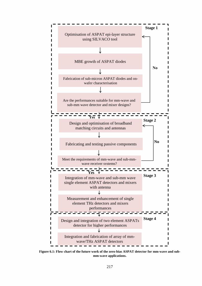
217
Figure 6.1: Flow chart of the future work of the zero-bias ASPAT detector for mm-wave and sub-
mm-wave applications.
Stage 1
Stage 2
Optimisation of ASPAT epi-layer structure
using SILVACO tool
MBE growth of ASPAT diodes
Fabrication of sub-micron ASPAT diodes and on-
wafer characterisation
Are the performances suitable for mm-wave and
sub-mm wave detector and mixer designs?
Design and optimisation of broadband
matching circuits and antennas
Integration of mm-wave and sub-mm wave
single element ASPAT detectors and mixers
with antenna
Measurement and enhancement of single
element THz detectors and mixers
performances
Yes
No
Stage 3
Stage 4
Yes
No Fabricating and testing passive components
Meet the requirements of mm-wave and sub-mm-
wave receiver systems?
Design and integration of two element ASPATs
detector for higher performances
Integration and fabrication of array of mm-
wave/THz ASPAT detectors

218
1- Design and fabrication of sub-micron ASPAT diodes with smaller junction
capacitance and high cut-off frequency up to 1THz. It has been shown that the cut-off
frequency is constrained by the series resistance and most importantly, the non-linear
resistance of the un-depleted spacer layer under zero and forward bias. Therefore, the
next step would be the growth and fabrication of ASPAT diodes with spacer ratio of
(20:1) to examine the variation of the non-linear resistance and junction capacitance with
respect to the thickness of the spacer. It is necessary to conduct such a study for the
GaAs/AlAs and InGaAs/AlAs ASPAT epi-layer structures to figure out the optimum
spacer thickness, which gives the highest cut-off frequency and better non-linear
characteristics. The noise characteristics of the discrete ASPAT devices should also be
investigated and compared to the other reported diodes.
2- The other approach is to manipulate the ASPAT layer structure to improve the
curvature coefficient and junction resistance. In chapter 3, an experimental investigation
verified by several fabricated and tested GaAs/AlAs ASPAT diodes was conducted to
study the variation of the non-linear characteristics with respect to AlAs barrier. This
principle will be extended to examine other key layers of the ASPAT diodes. The
measurement of ASPAT unmatched sensitivity at low frequency will allow estimating
the exact values of curvature coefficient, which should be close to the extracted value
from the DC characteristics. The work will be continued through employing a physical
simulation tool such as SILVACO ATLAS to study and understand the behaviour of
such tunnel diodes concerning the variation of the other layers (emitter or collector) of
different material-based devices. The physical modelling is hugely beneficial before the
costly production process.
3- Recently, the metamorphic buffer technique has attracted attention due to its
applicability in the fabrication of different III-V devices on substrates with large lattice
mismatch. The main advantage of such a technique is the use of a well-matured GaAs IC
fabrication technology. Moreover, the lower cost of the GaAs substrate and it’s
availability in larger size compared to InP makes the growth of metamorphic
In0.53Ga0.47As/AlAs mASPAT attractive. At the time of writing the thesis, metamorphic
In0.53Ga0.47As/AlAs ASPAT structures have been grown on a GaAs platform and then
fabricated into different mesa area sizes. The preliminary results showed that the
curvature coefficients is ~14V-1
at zero-bias, which is close enough to value extracted for
the standard In0.53Ga0.47As/AlAs ASPAT grown on InP substrate. The focus now is to

219
perform the RF characterisation and extract the intrinsic parameters of the devices at
different bias.
4- From the circuit perspective, optimising the matching networks and antennas would
help to improve the total performances of the detector and mixer circuits. Alternative
matching circuit based radial stubs or filters can be explored with the help of the
momentum of method and FEM simulations embedded in the Keysight-ADS and EMPro
commercial software.
5- More importantly, is the effect of the parasitic components associated with passive
elements at high-frequency. The growth and fabrication of the future ASPAT diodes
would be on a thinner substrate in the range of 100 to 150µm which would contribute to
minimising the platform losses as it was verified by the simulation work done in chapter
three.
6- The eventual aim of this work is the integration of ASPAT detector with a broadband
antenna to realise a zero-bias and low noise mm/THz wave detection circuits. The use of
CST studio and EMPro tools should be carried out to design different antenna structures
such as Quasi-Yagi and dipole antennas with various resonance frequencies. Meanwhile,
the designated 77GHz and 250GHz bow-tie antennas should be fabricated and tested in
terms of the return loss and radiation gain. As future work, antennas can be designed
with a reactive part that cancels the capacitive effect of ASPAT diode, and so, more
power is delivered without the need of a complex matching network.
The ambition of this work is to push the sensitivity of the mm/THz waves ASPAT
detector as high as possible and also to increase their dynamic range that would, in turn,
improve the signal-to-noise ratio of the receiver system. One of the possible techniques is
to incorporate two ASPAT diodes in parallel to enhance the generated DC voltage of the
detector. Smaller mesa area devices are required to compensate for the increase of
junction capacitance. Two devices in parallel reduce the total junction resistance of the
detector and improve the speed response of the receiver.
Also, it is desirable to make the design of the matching circuit less complicated. The
challenge is to produce tunnel diodes with similar DC and RF characteristics to mitigate
any performance degradation. We already have proved the high precision of controlling
the epi-layer growth through conducting different tunnelling structures. An array of THz
integrated ASPAT detectors can be formed for applications in spatial power combining,

220
massive MIMO communications and imaging arrays. Overall, it can be claimed that the
performances obtained from the discrete ASPAT diodes and microwave detectors are
eminently good to warrant pursuit the proposed ideas and justifying continuing research
into tunnel ASPAT diode application in millimetre and sub-millimetre wave detection
circuits.
6.2.2 Fabrication of the Optimised APD and PIN Photodetectors
The next step in APD/PIN research should be the fabrication and measurement of the
optimised APD and PIN photodetectors for 25Gb/s and 50Gb/s data rate application,
respectively. Distributed Bragg reflector layers can be buried at the bottom of the epi-
layers structure of the diodes to reflect the light and enhance the DC responsivity. The
multiplication gain of the optimised APD can be enhanced using amplification circuit
such as the widely known trans-impedance amplifier (TIA). The latter would also help to
enhance the DC responsivity of the PIN diode for longer distance high-data-rate
applications. In terms of the physical model work, the analysis of the temperature
dependency of the APD would be an interesting topic to pursue. From the design
approach, the validated and proven physical models can be exploited to simulate the
performances of different APD structures having different doping concentration and
thickness. In particular, the charge sheet and multiplication layers as they dominantly
control the field distribution across the structure. The key factor (𝑘𝑟𝑎𝑡𝑖𝑜) of the avalanche
multiplication process should also be investigated and optimised for lower excess noise.
Bandwidth improvement techniques should also be considered to enhance the 3-dB
bandwidth of the proposed APD and PIN photodetectors. Among them is the passive
peaking method utilising capacitive or inductive element in series or parallel with the
photodetector. The technique was widely used and showed an improvement in the
bandwidth by a factor of two [282-284].

221
APPENDICES
APPENDIX-A: QFN Circuit
ASPAT diode

222
APPENDIX-B: Lab View programme
A LabVIEW code was written by Dr Sexton to control the frequency and power of the
input RF signal as well as viewing the output voltage versus the RF frequency, as shown
below.
APPENDIX-C: Test Structure Used in the Mask
Below is the fabricated test structure in the mask as well as the measured and simulated
𝑆11 and 𝑆21 data.

223
APPENDIX-D: Measured and Simulated 𝑺𝟏𝟏 of the Fabricated 30GHz ASPAT
Detector with Open Stub Matching Network
-35
-30
-25
-20
-15
-10
-5
0
0 10 20 30 40
dB
Frequency (GHz)
Measured S11
Simulated S11
Measured S21
Simulated S21
-20
-15
-10
-5
0
27 29 31 33 35
dB
Frequency (GHz)
Measured S11
Simulated S11

224
REFERENCES
[1] T. Miyamoto, A. Yamaguchi, and T. J. J. J. o. A. P. Mukai, "Terahertz imaging
system with resonant tunneling diodes," vol. 55, no. 3, p. 032201, 2016.
[2] B. Jackson, "Subharmonic mixers in CMOS microwave integrated circuits,"
2009.
[3] H.-J. Song and T. Nagatsuma, "Present and future of terahertz communications,"
IEEE transactions on terahertz science and technology, vol. 1, no. 1, pp. 256-
263, 2011.
[4] T. Kleine-Ostmann and T. Nagatsuma, "A review on terahertz communications
research," Journal of Infrared, Millimeter, and Terahertz Waves, vol. 32, no. 2,
pp. 143-171, 2011.
[5] J. Wang, "Monolithic microwave/millimetrewave integrated circuit resonant
tunnelling diode dources with around a milliwatt output power," University of
Glasgow, 2014.
[6] S. Solutions, "RF Diode Design Guide," ed, 2017.
[7] I. Oprea, A. Walber, O. Cojocari, H. Gibson, R. Zimmermann, and H. Hartnagel,
"183 GHz mixer on InGaAs Schottky diodes," Proc. ISSTT, pp. 159-160, 2010.
[8] S. Khanal et al., "Characterisation of low-barrier Schottky diodes for millimeter
wave mixer applications," in 2016 Global Symposium on Millimeter Waves
(GSMM) & ESA Workshop on Millimetre-Wave Technology and Applications,
2016, pp. 1-4: IEEE.
[9] Y. Changfei, Z. Ming, L. Yunsheng, and X. Conghai, "Millimeter wave
broadband high sensitivity detectors with zero-bias Schottky diodes," Journal of
Semiconductors, vol. 36, no. 6, p. 065002, 2015.
[10] J. J. Lynch, J. N. Schulman, and H. P. Moyer, "Low noise direct detection sensors
for millimeter wave imaging," in 2006 IEEE Compound Semiconductor
Integrated Circuit Symposium, 2006, pp. 215-218: IEEE.
[11] H. Moyer et al., "W-band Sb-diode detector MMICs for passive millimeter wave
imaging," IEEE Microwave and Wireless Components Letters, vol. 18, no. 10, pp.
686-688, 2008.
[12] J. J. Lynch et al., "Passive millimeter-wave imaging module with preamplified
zero-bias detection," IEEE Transactions on Microwave Theory and Techniques,
vol. 56, no. 7, pp. 1592-1600, 2008.
[13] R. T. Syme, M. J. Kelly, M. Robinson, R. Smith, and I. Dale, "Novel GaAs/AlAs
tunnel structures as microwave detectors," in Semiconductors' 92, 1992, pp. 46-
56: International Society for Optics and Photonics.
[14] M. Missous, M. J. Kelly, and J. J. I. E. D. L. Sexton, "Extremely uniform tunnel
barriers for low-cost device manufacture," vol. 36, no. 6, pp. 543-545, 2015.
[15] M. R. Abdullah, Y. Wang, J. Sexton, M. Missous, and M. Kelly, "GaAs/AlAs
tunnelling structure: Temperature dependence of ASPAT detectors," in
Millimeter Waves and THz Technology Workshop (UCMMT), 2015 8th UK,
Europe, China, 2015, pp. 1-4: IEEE.
[16] Y. Wang, M. R. R. Abdullah, J. Sexton, and M. Missous, "Temperature
dependence characteristics of In0. 53Ga0. 47As/AlAs asymmetric spacer-layer
tunnel (ASPAT) diode detectors," in Millimeter Waves and THz Technology
Workshop (UCMMT), 2015 8th UK, Europe, China, 2015, pp. 1-4: IEEE.
[17] J. Bruder, J. Carlo, J. Gurney, and J. Gorman, "IEEE standard for letter
designations for radar-frequency bands," IEEE Aerospace & Electronic Systems
Society, pp. 1-3, 2003.

225
[18] Y. T. Lo and S. Lee, Antenna Handbook: Volume III Applications. Springer
Science & Business Media, 2012.
[19] H. Takahashi, A. Hirata, N. Kukutsu, Y. Kado, T. Kosugi, and K. Murata,
"Compact, Low-power, 120-GHz-band Wireless Link for 10-Gbit/s Data
Transmission," NTT Technical Review.[Online], 2009.
[20] E. Korczynski, "imec shows integrated 5G chip directions," ’Solid state
Technology magazine, 2018.
[21] M. Rojavin and M. Ziskin, "Medical application of millimetre waves," QJM:
monthly journal of the Association of Physicians, vol. 91, no. 1, pp. 57-66, 1998.
[22] F. Lin, W. Hu, and A. Li, "Millimeter-wave technology for medical applications,"
in 2012 IEEE MTT-S International Microwave Workshop Series on Millimeter
Wave Wireless Technology and Applications, 2012, pp. 1-1: IEEE.
[23] S. Oka, H. Togo, N. Kukutsu, and T. Nagatsuma, "Latest trends in millimeter-
wave imaging technology," Progress in Electromagnetics Research, vol. 1, pp.
197-204, 2008.
[24] P. Yadranjee Aghdam, "Sb-Heterostructure Backward Diode for Millimetre-
Wave Detection," 2012.
[25] H. Sato et al., "Development of 77 GHz millimeter wave passive imaging
camera," in SENSORS, 2009 IEEE, 2009, pp. 1632-1635: IEEE.
[26] M. Sato and K. Mizuno, "Millimeter-wave imaging sensor," in Microwave and
millimeter wave technologies from photonic bandgap devices to antenna and
applications: IntechOpen, 2010.
[27] R. S. t. group, "Security through technology," 2014.
[28] R. S. t. group, "Testing bumper material for installation of automotive radar
sensors," 2019.
[29] N. Kukutsu and Y. Kado, "Overview of millimeter and terahertz wave application
research," NTT Technical Review, vol. 7, no. 3, p. 6, 2009.
[30] A. Rogalski and F. Sizov, "Terahertz detectors and focal plane arrays," Opto-
electronics review, vol. 19, no. 3, pp. 346-404, 2011.
[31] T. Inata, S. Muto, Y. Nakata, T. Fujii, H. Ohnishi, and S. Hiyamizu, "Excellent
negative differential resistance of InAlAs/InGaAs resonant tunneling barrier
structures grown by MBE," Japanese journal of applied physics, vol. 25, no.
12A, p. L983, 1986.
[32] J. Bean, "Materials and technologies," ed: John Wiley & Sons, New York, 1990,
p. 13.
[33] S. G. Muttlak, O. S. Abdulwahid, J. Sexton, M. J. Kelly, and M. Missous,
"InGaAs/AlAs Resonant Tunneling Diodes for THz Applications: An
Experimental Investigation," IEEE Journal of the Electron Devices Society, vol.
6, pp. 254-262, 2018.
[34] M. A. B. M. Zawawi, "Advanced In0. 8Ga0. 2As/AlAs resonant tunneling diodes
for applications in integrated mm-waves MMIC oscillators," The University of
Manchester, 2015.
[35] S.-Y. Park et al., "Si/SiGe Resonant Interband Tunneling Diodes Incorporating
$\delta $-Doping Layers Grown by Chemical Vapor Deposition," IEEE Electron
Device Letters, vol. 30, no. 11, pp. 1173-1175, 2009.
[36] K.-S. Jang et al., "High performance Ge-on-Si avalanche photodetector," in
Optical Interconnects XVI, 2016, vol. 9753, p. 97531C: International Society for
Optics and Photonics.

226
[37] M. Huang et al., "Germanium on Silicon Avalanche Photodiode," IEEE Journal
of Selected Topics in Quantum Electronics, vol. 24, no. 2, pp. 3800911-3800911,
2018.
[38] J. E. Bowers, D. Dai, Y. Kang, and M. Morse, "High-gain high-sensitivity
resonant Ge/Si APD photodetectors," in Infrared Technology and Applications
XXXVI, 2010, vol. 7660, p. 76603H: International Society for Optics and
Photonics.
[39] J. Joo, S. Kim, I. G. Kim, K.-S. Jang, and G. Kim, "High-sensitivity 10 Gbps Ge-
on-Siphotoreceiveroperatingatλ~ 1.55μm,"Optics express, vol. 18, no. 16, pp.
16474-16479, 2010.
[40] N. Duan, T.-Y. Liow, A. E.-J. Lim, L. Ding, and G. Lo, "310 GHz gain-
bandwidth product Ge/Si avalanche photodetector for 1550 nm light detection,"
Optics express, vol. 20, no. 10, pp. 11031-11036, 2012.
[41] C. Li, C. Xue, Z. Liu, B. Cheng, C. Li, and Q. Wang, "High-bandwidth and high-
responsivity top-illuminated germanium photodiodes for optical interconnection,"
IEEE Transactions on Electron Devices, vol. 60, no. 3, pp. 1183-1187, 2013.
[42] S. Klinger, M. Berroth, M. Kaschel, M. Oehme, and E. Kasper, "Ge-on-Si pin
photodiodes with a 3-dB bandwidth of 49 GHz," IEEE Photonics Technology
Letters, vol. 21, no. 13, p. 920, 2009.
[43] Y. Kang et al., "Monolithic germanium/silicon avalanche photodiodes with 340
GHz gain–bandwidth product," Nature photonics, vol. 3, no. 1, pp. 59-63, 2009.
[44] S. M. Sze, "High-speed semiconductor devices," New York, Wiley-Interscience,
1990, 653 p. No individual items are abstracted in this volume., 1990.
[45] J. Karlovský, "The curvature coefficient of germanium tunnel and backward
diodes," Solid-State Electronics, vol. 10, no. 11, pp. 1109-1111, 1967.
[46] J. B. Hopkins, "Microwave backward diodes in InAs," Solid-State Electronics,
vol. 13, no. 5, pp. 697-705, 1970.
[47] T. Takahashi, M. Sato, Y. Nakasha, and N. Hara, "Sensitivity Improvement in
GaAsSb-Based Heterojunction Backward Diodes by Optimized Doping
Concentration," IEEE Transactions on Electron Devices, vol. 62, no. 6, pp. 1891-
1897, 2015.
[48] T. Takahashi, M. Sato, T. Hirose, and N. Hara, "Energy band control of GaAsSb-
based backward diodes to improve sensitivity of millimeter-wave detection,"
Japanese Journal of Applied Physics, vol. 49, no. 10R, p. 104101, 2010.
[49] J. N. Schulman, D. H. Chow, E. T. Croke, C. W. Pobanz, H. L. Dunlap, and C.
Haeussler, "Sb-heterostructure zero-bias diodes for direct detection beyond 100
GHz," in International Symposium on Optical Science and Technology, 2000, pp.
221-226: International Society for Optics and Photonics.
[50] Z. Zhang, R. Rajavel, P. Deelman, and P. Fay, "Sub-Micron Area Heterojunction
Backward Diode Millimeter-Wave Detectors With With 0.18pW/√Hz Noise
Equivalent Power," IEEE Microwave and Wireless Components Letters, vol. 21,
no. 5, pp. 267-269, 2011.
[51] S. Suzuki, M. Asada, A. Teranishi, H. Sugiyama, and H. Yokoyama,
"Fundamental oscillation of resonant tunneling diodes above 1 THz at room
temperature," Applied Physics Letters, vol. 97, no. 24, p. 242102, 2010.
[52] H. Kanaya, H. Shibayama, R. Sogabe, S. Suzuki, and M. Asada, "Fundamental
oscillation up to 1.31 THz in resonant tunneling diodes with thin well and
barriers," Applied Physics Express, vol. 5, no. 12, p. 124101, 2012.

227
[53] T. Maekawa, H. Kanaya, S. Suzuki, and M. Asada, "Oscillation up to 1.92 THz in
resonant tunneling diode by reduced conduction loss," Applied physics express,
vol. 9, no. 2, p. 024101, 2016.
[54] M. Piels, Si/Ge photodiodes for coherent and analog communication. University
of California, Santa Barbara, 2013.
[55] H. T. J. MEIER, "Design, characterization and simulation of avalanche
photodiodes," ETH ZURICH, 2011.
[56] K. Tanaka, A. Agata, and Y. Horiuchi, "IEEE 802.3 av 10G-EPON
standardization and its research and development status," Journal of Lightwave
Technology, vol. 28, no. 4, pp. 651-661, 2009.
[57] J. Yu, X. Li, and W. J. A. P. Zhou, "Tutorial: Broadband fiber-wireless
integration for 5G+ communication," vol. 3, no. 11, p. 111101, 2018.
[58] X. Pang et al., "25 Gbit/s QPSK hybrid fiber-wireless transmission in the W-band
(75–110 GHz) with remote antenna unit for in-building wireless networks," vol.
4, no. 3, pp. 691-698, 2012.
[59] A. Chowdhury, K. Chuang, H.-C. Chien, D. Yeh, J. Yu, and G.-K. Chang, "Field
demonstration of bi-directional millimeter wave RoF systems inter-operable with
60 GHz multi-gigabit CMOS transceivers for in-building HD video and data
delivery," in Optical Fiber Communication Conference, 2011, p. OThJ3: Optical
Society of America.
[60] C.-H. Ho et al., "50-Gb/s radio-over-fiber system employing MIMO and OFDM
modulation at 60 GHz," in Optical Fiber Communication Conference, 2012, p.
OM2B. 3: Optical Society of America.
[61] R. Syme, "Tunnelling devices as microwave mixers and detectors," Philosophical
Transactions of the Royal Society of London A: Mathematical, Physical and
Engineering Sciences, vol. 354, no. 1717, pp. 2351-2364, 1996.
[62] B. Williams, S. Kumar, Q. Hu, and J. Reno, "Resonant-phonon terahertz
quantum-cascade laser operating at 2.1 THz (/spl lambda//spl sime/141/spl
mu/m)," Electronics Letters, vol. 40, no. 7, pp. 431-433, 2004.
[63] A. Khalid et al., "$\hbox In _ 0.53\hbox Ga _ 0.47\hbox As $ Planar
Gunn Diodes Operating at a Fundamental Frequency of 164 GHz," IEEE Electron
Device Letters, vol. 34, no. 1, pp. 39-41, 2013.
[64] S.-J. Yeon, M. Park, J. Choi, and K. Seo, "610 GHz InAlAs/In 0.75 GaAs
metamorphic HEMTs with an ultra-short 15-nm-gate," in Electron Devices
Meeting, 2007. IEDM 2007. IEEE International, 2007, pp. 613-616: IEEE.
[65] J. Wang, "Monolithic microwave/millimetrewave integrated circuit resonant
tunnelling diode sources with around a milliwatt output power," University of
Glasgow, 2014.
[66] V. Doychinov, "Quantum Barrier Devices for Sub-Millimetre Wave Detection,"
University of Leeds, 2015.
[67] U. L. Rohde and M. Rudolph, RF/microwave circuit design for wireless
applications. John Wiley & Sons, 2013.
[68] D. V. George, P. M. Anthony, and R. L. Ulrich, "Microwave circuit design using
linear and nonlinear techniques," Wiley. New York, pp. 279-283, 1990.
[69] G. D. Vendelin, A. M. Pavio, and U. L. Rohde, Microwave circuit design using
linear and nonlinear techniques. John Wiley & Sons, 2005.
[70] A. Maalik and Z. Mahmood, "A novel C-band single diode mixer with ultra high
LO/RF and LO/IF isolation," in Electrical Engineering, 2007. ICEE'07.
International Conference on, 2007, pp. 1-6: IEEE.

228
[71] S. A. Maas, "Microwave mixers," Norwood, MA, Artech House, Inc., 1986, 368
p., vol. 1, 1986.
[72] F. Marki and C. Marki, "Mixer Basics Primer, A tutorial for RF & Microwave
Mixers," Application Note, 2010.
[73] F. Marki and C. Marki, "Mixer Basics Primer," Marki Microwave. USA.[Online].
Available: www. mar imicrowave. com/menus/appnotes/mixer_basics_primer.
pdf, 2010.
[74] J. M. Rollin, "Integrated Subharmonic Planar Schottky Diode Mixers for
Submillimetrewave Applications," University of Bath, 2015.
[75] B. Thomas et al., "An integrated 520–600 GHz sub-harmonic mixer and tripler
combination based on GaAs MMIC membrane planar Schottky diodes," in
Infrared Millimeter and Terahertz Waves (IRMMW-THz), 2010 35th
International Conference on, 2010, pp. 1-2: IEEE.
[76] P. Wilkinson et al., "A 664 GHz Sub-Harmonic Schottky Mixer," in Twenty-First
International Symposium on Space Terahertz Technology, 2010, vol. 1, p. 413.
[77] B. Thomas, A. Maestrini, and D. Matheson, "Design of an 874 GHz biasable sub-
harmonic mixer based on MMIC membrane planar schottky diodes. Infrared," in
33rd International Conference on Millimeter and Terahertz Waves, 2008.
[78] I. Rosu, "RF Technical Articles," Electronic article
[79] R. Circa, "Study on Resistive Mixer Circuits in Reconfigurable Mobile
Communication Systems," 2008.
[80] X.-F. Yang, G. Wang, L. Wang, and B. Zhang, "380 GHz Sub-Harmonically
Pumped Mixer Based on Anti-Parallel Planar Schottky Diode," Progress In
Electromagnetics Research Letters, vol. 46, pp. 1-6, 2014.
[81] J. V. Siles, J. Grajal, and V. Krozer, "Design of subharmonically pumped
schottky mixers for submillimetre-wave applications," in European Microwave
Integrated Circuits Conference, 2006. The 1st, 2006, pp. 145-148: IEEE.
[82] M. Cohn, J. E. Degenford, and B. A. Newman, "Harmonic mixing with an
antiparallel diode pair," Microwave Theory and Techniques, IEEE Transactions
on, vol. 23, no. 8, pp. 667-673, 1975.
[83] A. A. Dias, D. Consonni, and M. Luqueze, "High isolation sub-harmonic mixer,"
in Microwave and Optoelectronics Conference, 1999. SBMO/IEEE MTT-S, APS
and LEOS-IMOC'99. International, 1999, vol. 2, pp. 378-381: IEEE.
[84] M. Morschbach, A. Müller, C. Schöllhorn, M. Oehme, T. Buck, and E. Kasper,
"Integrated silicon Schottky mixer diodes with cutoff frequencies above 1 THz,"
Microwave Theory and Techniques, IEEE Transactions on, vol. 53, no. 6, pp.
2013-2018, 2005.
[85] C. Liu, Q. Li, Y. Li, X. Li, H. Liu, and Y.-Z. Xiong, "Design of 340 GHz 2× and
4× Sub-Harmonic Mixers Using Schottky Barrier Diodes in Silicon-Based
Technology," Micromachines, vol. 6, no. 5, pp. 592-599, 2015.
[86] M. Morschbach, A. Muller, C. Schollhorn, M. Oehme, T. Buck, and E. Kasper,
"Integrated silicon Schottky mixer diodes with cutoff frequencies above 1 THz,"
IEEE Transactions on Microwave Theory and Techniques, vol. 53, no. 6, pp.
2013-2018, 2005.
[87] S.-H. Hung, K.-W. Cheng, and Y.-H. Wang, "Broadband sub-harmonic mixer
with a compact band pass filter," in Microwave Conference Proceedings (APMC),
2012 Asia-Pacific, 2012, pp. 208-210: IEEE.
[88] R. Syme, "Microwave detection using GaAs," GEC journal of research, vol. 11,
no. 1, pp. 12-23, 1993.

229
[89] G. Carpintero, E. Garcia-Munoz, H. Hartnagel, S. Preu, and A. Raisanen,
Semiconductor teraHertz technology: devices and systems at room temperature
operation. John Wiley & Sons, 2015.
[90] S. F. Adam, "Microwave theory and applications," 1969.
[91] M. Hrobak, Critical mm-wave components for synthetic automatic test systems.
Springer, 2015.
[92] N. Su, High-performance antimony-heterostructure backward diodes for
millimeter-wave detection and imaging. University of Notre Dame, 2008.
[93] R. Syme, "Microwave detection using GaAs/AlAs tunnel structures," GEC
journal of research, vol. 11, no. 1, pp. 12-23, 1993.
[94] M. Patrashin et al., "GaAsSb/InAlAs/InGaAs Tunnel Diodes for Millimeter Wave
Detection in 220–330-GHz Band," IEEE Transactions on Electron Devices, vol.
62, no. 3, pp. 1068-1071, 2015.
[95] M. Hrobak, M. Sterns, M. Schramm, W. Stein, and L.-P. Schmidt, "Planar zero
bias Schottky diode detector operating in the E-and W-band," in Microwave
Conference (EuMC), 2013 European, 2013, pp. 179-182: IEEE.
[96] V. I. Shashkin et al., "Millimeter-wave detectors based on antenna-coupled low-
barrier Schottky diodes," International Journal of Infrared and Millimeter Waves,
vol. 28, no. 11, pp. 945-952, 2007.
[97] R. Al Hadi, "Terahertz Integrated Circuits in Silicon Technologies," Universität
Wuppertal, Fakultät für Elektrotechnik, Informationstechnik und …,2018.
[98] B. S. Karasik and R. J. A. P. L. Cantor, "Demonstration of high optical sensitivity
in far-infrared hot-electron bolometer," vol. 98, no. 19, p. 193503, 2011.
[99] A. Cowley and H. Sorensen, "Quantitative comparison of solid-state microwave
detectors," IEEE Transactions on Microwave Theory and Techniques, vol. 14, no.
12, pp. 588-602, 1966.
[100] Y. Anand and W. J. Moroney, "Microwave mixer and detector diodes,"
Proceedings of the IEEE, vol. 59, no. 8, pp. 1182-1190, 1971.
[101] H.-P. A. Note, "923, Schottky Barrier Diode Video Detectors," ed: Hewlet
Packard, Nov, 1999.
[102] S. M. Sze and K. K. Ng, Physics of semiconductor devices. John wiley & sons,
2006.
[103] S. G. Muttlak, "Advanced THz Electronics Devices and Circuits," University of
Mnachester2015.
[104] M. R. R. B. Abdullah, "GaAs/AlAs ASPAT Diodes for Millimetre and Sub-
Millimetre Wave Applications," The University of Manchester (United
Kingdom), 2018.
[105] Y. Yan, Silicon-based tunnel diode technology. Citeseer, 2008.
[106] L. L. Chang, L. Esaki, and R. Tsu, "Resonant tunneling in semiconductor double
barriers," Applied physics letters, vol. 24, no. 12, pp. 593-595, 1974.
[107] W. Zhang, E. Brown, T. Growden, P. Berger, and R. Droopad, "A Nonlinear
Circuit Simulation of Switching Process in Resonant-Tunneling Diodes," IEEE
Transactions on Electron Devices, vol. 63, no. 12, pp. 4993-4997, 2016.
[108] J. S. Harris Jr, "The design of GaAs/AIAs resonant tunneling diodes with peak
current densities over 2 x 1 O5 A cma2," J. Appl. Phys, vol. 69, no. 5, 1991.
[109] M. Zawawi, "Advanced In0. 8Ga0. 2As/AlAs resonant tunneling diodes for
applications in integrated mm-waves MMIC oscillators," University of
Manchester, 2015.

230
[110] M. Asada and S. Suzuki, "Terahertz oscillators using electron devices—an
approach with resonant tunneling diodes," IEICE Electronics Express, vol. 8, no.
14, pp. 1110-1126, 2011.
[111] H. Kanaya, T. Maekawa, S. Suzuki, and M. Asada, "Structure dependence of
oscillation characteristics of resonant-tunneling-diode terahertz oscillators
associated with intrinsic and extrinsic delay times," Japanese Journal of Applied
Physics, vol. 54, no. 9, p. 094103, 2015.
[112] S. G. Muttlak, O. S. Abdulwahid, J. Sexton, M. J. Kelly, and M. Missous,
"InGaAs/AlAs Resonant Tunneling Diodes for THz Applications: An
Experimental Investigation," IEEE Journal of the Electron Devices Society, vol.
6, no. 1, pp. 254-262, 2018.
[113] J. M. L. Figueiredo, "Optoelectronic properties of resonant tunnelling diodes,"
2000.
[114] E. R. Brown, C. D. Parker, K. M. Molvar, and K. D. Stephan, "A quasioptically
stabilized resonant-tunneling-diode oscillator for the millimeter-and
submillimeter-wave regions," Microwave Theory and Techniques, IEEE
Transactions on, vol. 40, no. 5, pp. 846-850, 1992.
[115] E. Brown, C. Parker, A. Calawa, M. Manfra, and K. Molvar, "A quasioptical
resonant-tunneling-diode oscillator operating above 200 GHz," Microwave
Theory and Techniques, IEEE Transactions on, vol. 41, no. 4, pp. 720-722, 1993.
[116] A. Molnar et al., "Submm-wave monolithic RTD oscillator arrays to 650 GHz,"
in Electron Devices Meeting, 1996. IEDM'96., International, 1996, pp. 940-942:
IEEE.
[117] S. Suzuki, M. Shiraishi, H. Shibayama, and M. Asada, "High-power operation of
terahertz oscillators with resonant tunneling diodes using impedance-matched
antennas and array configuration," Selected Topics in Quantum Electronics, IEEE
Journal of, vol. 19, no. 1, pp. 8500108-8500108, 2013.
[118] S. Takahagi, H. Shin-ya, K. Asakawa, M. Saito, and M. Suhara, "Equivalent
circuit model of triple-barrier resonant tunneling diodes monolithically integrated
with bow-tie antennas and analysis of rectification properties towards ultra
wideband terahertz detections," Japanese Journal of Applied Physics, vol. 50, no.
1S2, p. 01BG01, 2011.
[119] V. Wilkinson, M. Kelly, and M. Carr, "Tunnel devices are not yet
manufacturable," Semiconductor science and technology, vol. 12, no. 1, p. 91,
1997.
[120] R. T. J. E. Syme, "Novel semiconductor tunnelling devices for microwave
applications," vol. 18, no. 3, pp. 90-95, 1994.
[121] M. J. Kelly, "Low cost manufacture of high frequency tunnel device systems," in
Terahertz Electronics Proceedings, 2002. IEEE Tenth International Conference
on, 2002, pp. 85-88: IEEE.
[122] T. Hori, T. Ozono, N. Orihashi, and M. Asada, "Frequency mixing characteristics
of room temperature resonant tunneling diodes at 100 and 200 GHz," Journal of
applied physics, vol. 99, no. 6, p. 064508, 2006.
[123] C. Kyono, V. Kesan, D. Neikirk, C. Maziar, and B. Streetman, "Dependence of
apparent barrier height on barrier thickness for perpendicular transport in
AlAs/GaAs single‐barrier structures grown by molecular beam epitaxy," Applied
physics letters, vol. 54, no. 6, pp. 549-551, 1989.
[124] Y. P. Varshni, "Temperature dependence of the energy gap in semiconductors,"
physica, vol. 34, no. 1, pp. 149-154, 1967.

231
[125] K. Z. Ariffin et al., "Investigations of Asymmetric Spacer Tunnel Layer Diodes
for High-Frequency Applications," IEEE Transactions on Electron Devices, vol.
65, no. 1, pp. 64-71, 2018.
[126] N. Tuomisto, A. Zugarramurdi, and M. J. J. J. o. A. P. Puska, "Modeling of
electron tunneling through a tilted potential barrier," vol. 121, no. 13, p. 134304,
2017.
[127] L. Vivien et al., "Zero-bias 40Gbit/s germanium waveguide photodetector on
silicon," Optics express, vol. 20, no. 2, pp. 1096-1101, 2012.
[128] L. Vivien et al., "42 GHz pin Germanium photodetector integrated in a silicon-
on-insulator waveguide," Optics express, vol. 17, no. 8, pp. 6252-6257, 2009.
[129] J.-W. Shi, Y.-H. Cheng, J.-M. Wun, K.-L. Chi, Y.-M. Hsin, and S. D. Benjamin,
"High-Speed, high-efficiency, large-area pin photodiode for application to optical
interconnects from 0.85 to 1.55 μm Wavelengths," Journal of Lightwave
Technology, vol. 31, no. 24, pp. 3956-3961, 2013.
[130] L. Virot et al., "High-performance waveguide-integrated germanium PIN
photodiodes for optical communication applications," Photonics Research, vol. 1,
no. 3, pp. 140-147, 2013.
[131] Z. Huang et al., "25 Gbps low-voltage waveguide Si–Ge avalanche photodiode,"
Optica, vol. 3, no. 8, pp. 793-798, 2016.
[132] K. Makita, T. Nakata, K. Shiba, and T. Takeuchi, "40Gbps waveguide
photodiodes," NEC J. Adv. Tech, vol. 2, no. 3, pp. 234-240, 2005.
[133] O. Kharraz and D. Forsyth, "Performance comparisons between PIN and APD
photodetectors for use in optical communication systems," Optik-International
Journal for Light and Electron Optics, vol. 124, no. 13, pp. 1493-1498, 2013.
[134] P. Yuan et al., "Impact ionization characteristics of III-V semiconductors for a
wide range of multiplication region thicknesses," IEEE journal of quantum
electronics, vol. 36, no. 2, pp. 198-204, 2000.
[135] M. A. Saleh et al., "Impact-ionization and noise characteristics of thin III-V
avalanche photodiodes," IEEE Transactions on Electron Devices, vol. 48, no. 12,
pp. 2722-2731, 2001.
[136] G. Kinsey, J. Campbell, and A. Dentai, "Waveguide avalanche photodiode
operating at 1.55 μm with a gain-bandwidth product of 320 GHz," IEEE
Photonics Technology Letters, vol. 13, no. 8, pp. 842-844, 2001.
[137] Y.-H. Chen et al., "Top-illuminated In0. 52Al0. 48As-based avalanche
photodiode with dual charge layers for high-speed and low dark current
performances," IEEE Journal of Selected Topics in Quantum Electronics, vol. 24,
no. 2, pp. 1-8, 2018.
[138] X. Meng, C. H. Tan, S. Dimler, J. P. David, and J. S. Ng, "1550 nm
InGaAs/InAlAs single photon avalanche diode at room temperature," Optics
Express, vol. 22, no. 19, pp. 22608-22615, 2014.
[139] F. Ma, N. Li, and J. C. Campbell, "Monte Carlo simulations of the bandwidth of
InAlAs avalanche photodiodes," IEEE Transactions on Electron Devices, vol. 50,
no. 11, pp. 2291-2294, 2003.
[140] L. J. J. Tan et al., "Temperature dependence of avalanche breakdown in InP and
InAlAs," IEEE Journal of Quantum Electronics, vol. 46, no. 8, pp. 1153-1157,
2010.
[141] D. Haško, J. Kováč, F. Uherek, J. Škriniarová, J. Jakabovič, and L. Peternai,
"Avalanche photodiode with sectional InGaAsP/InP charge layer,"
Microelectronics journal, vol. 37, no. 6, pp. 483-486, 2006.

232
[142] M. Azadeh, "PIN and APD Detectors," in Fiber Optics Engineering: Springer,
2009, pp. 157-175.
[143] H. Ando, H. Kanbe, M. Ito, and T. Kaneda, "Tunneling current in InGaAs and
optimum design for InGaAs/InP avalanche photodiode," Japanese Journal of
Applied Physics, vol. 19, no. 6, p. L277, 1980.
[144] G. Stillman and C. Wolfe, "Avalanche photodiodes," Semiconductors and
semimetals, vol. 12, pp. 291-393, 1977.
[145] S. Xie, "Design and characterisation of InGaAs high speed photodiodes,
InGaAs/InAlAs avalanche photodiodes and novel AlAsSb based avalanche
photodiodes," University of Sheffield, 2012.
[146] H. Photonics, "Characteristics and use of Si APD (Avalanche Photodiode)," Solid
State Division, 2000.
[147] S. Selberherr, Analysis and simulation of semiconductor devices. Springer
Science & Business Media, 2012.
[148] R. Van Overstraeten and H. J. S.-S. E. De Man, "Measurement of the ionization
rates in diffused silicon pn junctions," vol. 13, no. 5, pp. 583-608, 1970.
[149] K. Li et al., "Low Avalanche Noise Characteristics in Thin InP p^+-in^+ Diodes
with Electron Initiated Multiplication," IEEE Photonics Technology Letters, vol.
11, no. 3, 1999.
[150] I. Watanabe, T. Torikai, K. Makita, K. Fukushima, and T. Uji, "Impact ionization
rates in (100) Al (0.48) In (0.52) As," IEEE Electron Device Letters, vol. 11, p.
437, 1990.
[151] J. C. Campbell, "Recent advances in telecommunications avalanche
photodiodes," Journal of Lightwave Technology, vol. 25, no. 1, pp. 109-121,
2007.
[152] K.-S. Jang et al., "High performance Ge-on-Si Avalanche photodetector," in SPIE
OPTO, 2016, pp. 97531C-97531C-6: International Society for Optics and
Photonics.
[153] M. Bitter, "InP/InGaAs pin-photodiode arrays for parallel optical interconnects
and monolithic InP/InGaAs pin/HBT optical receivers for 10-Gb/s and 40-Gb/s,"
ETH Zurich, 2000.
[154] G. P. Agrawal, Fiber-optic communication systems. John Wiley & Sons, 2012.
[155] M. Oehme, J. Werner, E. Kasper, M. Jutzi, and M. Berroth, "High bandwidth Ge
p-i-n photodetector integrated on Si," Applied physics letters, vol. 89, no. 7, p.
071117, 2006.
[156] T. Yin et al., "31 GHz Ge nip waveguide photodetectors on Silicon-on-Insulator
substrate," Optics Express, vol. 15, no. 21, pp. 13965-13971, 2007.
[157] M. Huang et al., "Breakthrough of 25Gb/s germanium on silicon avalanche
photodiode," in Optical Fiber Communication Conference, 2016, p. Tu2D. 2:
Optical Society of America.
[158] L. M. Giovane, H.-C. Luan, A. M. Agarwal, and L. C. J. A. P. L. Kimerling,
"Correlation between leakage current density and threading dislocation density in
SiGe pin diodes grown on relaxed graded buffer layers," vol. 78, no. 4, pp. 541-
543, 2001.
[159] P. S. Menon, A. A. Ehsan, and S. Shaari, Modeling and Optimization of Three-
Dimensional Interdigitated Lateral pin Photodiodes Based on In0. 53Ga0. 47As
Absorbers for Optical Communications. INTECH Open Access Publisher, 2011.
[160] Y.-S. Wang et al., "High-speed InGaAs pin photodetector with planar buried
heterostructure," IEEE Transactions on Electron Devices, vol. 56, no. 6, pp.
1347-1350, 2009.

233
[161] Y. Zhao et al., "InGaAs–InP avalanche photodiodes with dark current limited by
generation-recombination," Optics express, vol. 19, no. 9, pp. 8546-8556, 2011.
[162] A. Suzuki, A. Yamada, T. Yokotsuka, K. Idota, and Y. Ohki, "Dark current
reduction of avalanche photodiode using optimized InGaAsP/InAlAs superlattice
structure," Japanese journal of applied physics, vol. 41, no. 2S, p. 1182, 2002.
[163] K. Kato, "Ultrawide-band/high-frequency photodetectors," IEEE transactions on
Microwave Theory and Techniques, vol. 47, no. 7, pp. 1265-1281, 1999.
[164] J. Xie, J. S. Ng, and C. H. Tan, "An InGaAs/AlAsSb avalanche photodiode with a
small temperature coefficient of breakdown," IEEE Photonics Journal, vol. 5, no.
4, pp. 6800706-6800706, 2013.
[165] M. M. Hayat, P. Zarkesh-Ha, G. El-Howayek, R. Efroymson, and J. C. Campbell,
"Breaking the buildup-time limit of sensitivity in avalanche photodiodes by
dynamic biasing," Optics express, vol. 23, no. 18, pp. 24035-24041, 2015.
[166] J. Ng et al., "Effect of dead space on avalanche speed [APDs]," IEEE
Transactions on Electron Devices, vol. 49, no. 4, pp. 544-549, 2002.
[167] P. Hambleton, B. Ng, S. Plimmer, J. David, and G. Rees, "The effects of nonlocal
impact ionization on the speed of avalanche photodiodes," IEEE Transactions on
Electron Devices, vol. 50, no. 2, pp. 347-351, 2003.
[168] K. S. Hyun, C. Y. Park, and H. M. Kim, "Temperature dependent breakdown
characteristics in InP/InGaAs avalanche photodiodes," Japanese journal of
applied physics, vol. 35, no. 3A, p. L301, 1996.
[169] M. Nada, T. Hoshi, S. Kanazawa, T. Hashimoto, and H. Matsuzaki, "56-Gbit/s
40-km optical-amplifier-less transmission with NRZ format using high-speed
avalanche photodiodes," in Optical Fiber Communication Conference, 2016, p.
Tu2D. 1: Optical Society of America.
[170] M. Nada, T. Yoshimatsu, Y. Muramoto, H. Yokoyama, and H. Matsuzaki,
"Design and performance of high-speed avalanche photodiodes for 100-Gb/s
systems and beyond," Journal of Lightwave Technology, vol. 33, no. 5, pp. 984-
990, 2015.
[171] M. Nada, Y. Yamada, and H. Matsuzaki, "Responsivity-Bandwidth Limit of
Avalanche Photodiodes: Toward Future Ethernet Systems," IEEE Journal of
Selected Topics in Quantum Electronics, vol. 24, no. 2, pp. 1-11, 2018.
[172] M. Nada, T. Hoshi, H. Yamazaki, T. Hashimoto, and H. Matsuzaki, "Linearity
improvement of high-speed avalanche photodiodes using thin depleted absorber
operating with higher order modulation format," Optics express, vol. 23, no. 21,
pp. 27715-27723, 2015.
[173] W. Sun, X. Zheng, and J. C. Campbell, "Study of Excess Noise Factor Under
Nonlocal Effect in Avalanche Photodiodes," IEEE Photonics Technology Letters,
vol. 26, no. 21, pp. 2150-2153, 2014.
[174] R. McIntrye, "Multiplication noise in uniform avalanche photodiodes," IEEE
Trans. Electron. Dev, vol. 13, no. 1, pp. 164-168, 1966.
[175] S. Marsh, "Practical MMIC Design. Artech House," ed: Inc, 2006.
[176] H. Berger, "Models for contacts to planar devices," Solid-State Electronics, vol.
15, no. 2, pp. 145-158, 1972.
[177] G. Reeves and H. Harrison, "Obtaining the specific contact resistance from
transmission line model measurements," IEEE Electron device letters, vol. 3, no.
5, pp. 111-113, 1982.
[178] Y. Wang, "In0. 53Ga0. 47As-In0. 52Al0. 48As Multiple Quantum Well THz
Photoconductive Switches and In0. 53Ga0. 47As-AlAs Asymmetric Spacer Layer
Tunnel (ASPAT) Diodes for THz Electronics," University of Manchester, 2017.

234
[179] M. Missous, M. J. Kelly, and J. Sexton, "Extremely uniform tunnel barriers for
low-cost device manufacture," IEEE Electron Device Letters, vol. 36, no. 6, pp.
543-545, 2015.
[180] A. Gopinath, "Losses in coplanar waveguides," IEEE Transactions on Microwave
Theory and Techniques, vol. 30, no. 7, pp. 1101-1104, 1982.
[181] R. A. Pucel, "Design considerations for monolithic microwave circuits," IEEE
Transactions on Microwave Theory and Techniques, vol. 29, no. 6, pp. 513-534,
1981.
[182] M. Y. Frankel, S. Gupta, J. A. Valdmanis, and G. A. Mourou, "Terahertz
attenuation and dispersion characteristics of coplanar transmission lines," IEEE
Transactions on Microwave Theory and Techniques, vol. 39, no. 6, pp. 910-916,
1991.
[183] M. Koolen, J. Geelen, and M. Versleijen, "An improved de-embedding technique
for on-wafer high-frequency characterization," in Proceedings of the 1991
Bipolar Circuits and Technology Meeting, 1991, pp. 188-191: IEEE.
[184] W. L. Bishop, E. Meiburg, R. Mattauch, T. W. Crowe, and L. Poli, "A micron-
thickness, planar Schottky diode chip for terahertz applications with theoretical
minimum parasitic capacitance," in IEEE International Digest on Microwave
Symposium, 1990, pp. 1305-1308: IEEE.
[185] I. Wolff, Coplanar microwave integrated circuits. John Wiley & Sons, 2006.
[186] T. W. Crowe, "GaAs Schottky barrier mixer diodes for the frequency range 1–10
THz," International Journal of Infrared and Millimeter Waves, vol. 10, no. 7, pp.
765-777, 1989.
[187] J. T. Louhi and A. V. Raisanen, "On the modeling and optimization of Schottky
varactor frequency multipliers at submillimeter wavelengths," IEEE transactions
on microwave theory and techniques, vol. 43, no. 4, pp. 922-926, 1995.
[188] E. Schlecht, F. Maiwald, G. Chattopadhyay, S. Martin, and I. Mehdi, "Design
considerations for heavily-doped cryogenic Schottky diode varactor multipliers,"
2001.
[189] R. Lake and J. Yang, "A physics based model for the RTD quantum capacitance,"
IEEE Transactions on Electron Devices, vol. 50, no. 3, pp. 785-789, 2003.
[190] S. Diebold et al., "Modeling and Simulation of Terahertz Resonant Tunneling
Diode-Based Circuits," IEEE TRANSACTIONS ON TERAHERTZ SCIENCE AND
TECHNOLOGY, vol. 6, SEPTEMBER 2016.
[191] A. Y. Tang and J. Stake, "Impact of eddy currents and crowding effects on high-
frequency losses in planar Schottky diodes," IEEE Transactions on Electron
Devices, vol. 58, no. 10, pp. 3260-3269, 2011.
[192] J. Bruston et al., "Development of 200-GHz to 2.7-THz multiplier chains for
submillimeter-wave heterodyne receivers," in UV, Optical, and IR Space
Telescopes and Instruments, 2000, vol. 4013, pp. 285-296: International Society
for Optics and Photonics.
[193] I. D. Robertson and S. Lucyszyn, RFIC and MMIC Design and Technology (no.
13). Iet, 2001.
[194] S. Mao, S. Jones, and G. D. Vendelin, "Millimeter-wave integrated circuits,"
IEEE Transactions on Microwave Theory and Techniques, vol. 16, no. 7, pp. 455-
461, 1968.
[195] W. Lee, "Fast time-and frequency-domain finite-element methods for
electromagnetic analysis," 2016.
[196] A. Technologies, "Theory of operation for momentum," ADS 2011 Help, 2011.

235
[197] S. Alexandrou, C.-C. Wang, M. Currie, R. Sobolewski, and T. Y. Hsiang, "Loss
and dispersion at subterahertz frequencies in coplanar waveguides with varying
ground-plane widths," in Technologies for Optical Fiber Communications, 1994,
vol. 2149, pp. 108-119: International Society for Optics and Photonics.
[198] F. Aghamoradi, "The development of high quality passive components for sub-
millimetre wave applications," University of Glasgow, 2012.
[199] R. Simons and R. N. Simons, Coplanar waveguide circuits, components, and
systems. Wiley Online Library, 2001.
[200] M. Riaziat, R. Majidi-Ahy, and I.-J. Feng, "Propagation modes and dispersion
characteristics of coplanar waveguides," IEEE transactions on microwave theory
and techniques, vol. 38, no. 3, pp. 245-251, 1990.
[201] S. Arshad, "Low-Power Wideband InP-Based Low Noise Amplifiers for the
Square Kilometre Array Radio Telescope," The University of Manchester, 2009.
[202] L. Wang, R.-M. Xu, and B. Yan, "MIM capacitor simple scalable model
determination for MMIC application on GaAs," Progress In Electromagnetics
Research, vol. 66, pp. 173-178, 2006.
[203] D. Gruner, Z. Zhang, V. Subramanian, F. Korndoerfer, and G. Boeck, "Lumped
element MIM capacitor model for Si-RFICs," in 2007 SBMO/IEEE MTT-S
International Microwave and Optoelectronics Conference, 2007, pp. 149-152:
IEEE.
[204] K. Beilenhoff, H. Klingbeil, W. Heinrich, and H. L. Hartnagel, "Open and short
circuits in coplanar MMIC's," IEEE Transactions on microwave theory and
techniques, vol. 41, no. 9, pp. 1534-1537, 1993.
[205] G. E. Ponchak and L. P. Katehi, "Open-and short-circuit terminated series stubs
in finite-width coplanar waveguide on silicon," IEEE transactions on microwave
theory and techniques, vol. 45, no. 6, pp. 970-976, 1997.
[206] K. Beilenhoff, W. Heinrich, and H. L. Hartnagel, "Finite-difference analysis of
open and short circuits in coplanar MMICs including finite metallization
thickness and mode conversion," in 1992 IEEE MTT-S Microwave Symposium
Digest, 1992, pp. 103-106: IEEE.
[207] Y. Cao, Z. Jin, J. Ge, Y. Su, and X. Liu, "A symbolically defined InP double
heterojunction bipolar transistor large-signal model," Journal of Semiconductors,
vol. 30, no. 12, 2009.
[208] L. A. Tejedor-Alvarez, J. I. Alonso, and J. Gonzalez-Martin, "An ultrabroadband
microstrip detector up to 40 GHz," in Microwave Techniques, 2008. COMITE
2008. 14th Conference on, 2008, pp. 1-4: IEEE.
[209] J. Mou, X. Lv, Y. Yuan, and W. Yu, "Ka‐band quasioptical detectors based on
antenna‐integrated planar Schottky diodes," Microwave and Optical Technology
Letters, vol. 53, no. 9, pp. 2019-2022, 2011.
[210] R. A. Alhalabi, "High efficiency planar and RFIC-based antennas for millimeter-
wave communication systems," UC San Diego, 2010.
[211] J. L. Hesler, L. Liu, H. Xu, Y. Duan, and R. M. Weikle, "The development of
quasi-optical THz detectors," in 2008 33rd International Conference on Infrared,
Millimeter and Terahertz Waves, 2008, pp. 1-2: IEEE.
[212] D. Schoenherr et al., "Extremely broadband characterization of a Schottky diode
based THz detector," in 35th International Conference on Infrared, Millimeter,
and Terahertz Waves, 2010, pp. 1-2: IEEE.
[213] A. Semenov, O. Cojocari, H.-W. Hubers, F. Song, A. Klushin, and A.-S. Muller,
"Application of zero-bias quasi-optical Schottky-diode detectors for monitoring

236
short-pulse and weak terahertz radiation," IEEE Electron Device Letters, vol. 31,
no. 7, pp. 674-676, 2010.
[214] Y. Yuan, J.-C. Mou, D. Li, and X. Lv, "Design of integrated antenna-coupled
detector for MMW and Sub-MMW imaging," in 2010 International Conference
on Microwave and Millimeter Wave Technology, 2010, pp. 1315-1317: IEEE.
[215] S.Nahar,A.Muraviev,D.But,andM.M.Hella,"A220V/W,25pW/√HzNEP
bow-tie antenna-coupled pHEMT detector at 250 GHz," in 2016 41st
International Conference on Infrared, Millimeter, and Terahertz waves (IRMMW-
THz), 2016, pp. 1-2: IEEE.
[216] H. Liu, J. Yu, P. Huggard, and B. Alderman, "A multichannel THz detector using
integrated bow-tie antennas," International Journal of Antennas and Propagation,
vol. 2013, 2013.
[217] H. Kan, R. Waterhouse, A. Abbosh, and M. Bialkowski, "Simple broadband
planar CPW-fed quasi-Yagi antenna," IEEE Antennas and Wireless Propagation
Letters, vol. 6, pp. 18-20, 2007.
[218] N. Kaneda, W. Deal, Y. Qian, R. Waterhouse, and T. Itoh, "A broadband planar
quasi-Yagi antenna," IEEE Transactions on Antennas and Propagation, vol. 50,
no. 8, pp. 1158-1160, 2002.
[219] P. R. Grajek, B. Schoenlinner, and G. M. Rebeiz, "A 24-GHz high-gain Yagi-Uda
antenna array," IEEE Transactions on Antennas and Propagation, vol. 52, no. 5,
pp. 1257-1261, 2004.
[220] K. H. Alharbi, A. Ofiare, M. Kgwadi, A. Khalid, and E. Wasige, "Bow-tie
antenna for terahertz resonant tunnelling diode based oscillators on high dielectric
constant substrate," in 2015 11th Conference on Ph. D. Research in
Microelectronics and Electronics (PRIME), 2015, pp. 168-171: IEEE.
[221] J. Montero-de-Paz et al., "Compact modules for wireless communication systems
in the E-band (71–76 GHz)," Journal of Infrared, Millimeter, and Terahertz
Waves, vol. 34, no. 3-4, pp. 251-266, 2013.
[222] H. Ito, F. Nakajima, T. Ohno, T. Furuta, T. Nagatsuma, and T. Ishibashi, "InP-
based planar-antenna-integrated Schottky-barrier diode for millimeter-and sub-
millimeter-wave detection," Japanese Journal of Applied Physics, vol. 47, no. 8R,
p. 6256, 2008.
[223] J. Montero-de-Paz et al., "Compact Schottky barrier diode receiver for E-Band
(60–90 GHz) wireless communications," in 2012 IEEE International Topical
Meeting on Microwave Photonics, 2012, pp. 244-247: IEEE.
[224] S. Nadar et al., "High Performance Heterostructure Low Barrier Diodes for Sub-
THz Detection," IEEE Transactions on Terahertz Science and Technology, vol. 7,
no. 6, pp. 780-788, 2017.
[225] Ş.KarataşandŞ.Altındal, "Analysisof I–V characteristics on Au/n-type GaAs
Schottky structures in wide temperature range," Materials Science and
Engineering: B, vol. 122, no. 2, pp. 133-139, 2005.
[226] H.-W. Hübers and H. Röser, "Temperature dependence of the barrier height of
Pt/n-GaAs Schottky diodes," Journal of applied physics, vol. 84, no. 9, pp. 5326-
5330, 1998.
[227] M. Hoefle, K. Haehnsen, I. Oprea, O. Cojocari, A. Penirschke, and R. Jakoby,
"Compact and sensitive millimetre wave detectors based on low barrier Schottky
diodes on impedance matched planar antennas," Journal of Infrared, Millimeter,
and Terahertz Waves, vol. 35, no. 11, pp. 891-908, 2014.
[228] J. L. Hesler and T. W. Crowe, "Responsivity and noise measurements of zero-
bias Schottky diode detectors," Proc. ISSTT, pp. 89-92, 2007.

237
[229] S. M. Rahman, Z. Jiang, M. I. B. Shams, P. Fay, and L. Liu, "A G-Band
Monolithically Integrated Quasi-Optical Zero-Bias Detector Based on
Heterostructure Backward Diodes Using Submicrometer Airbridges," IEEE
Transactions on Microwave Theory and Techniques, 2017.
[230] V. Radisic, K. Leong, C. Zhang, K. Loi, and S. Sarkozy, "Demonstration of a
micro-integrated sub-millimeter-wave pixel," IEEE Transactions on Microwave
Theory and Techniques, vol. 61, no. 8, pp. 2949-2955, 2013.
[231] K. Technologies, "423B, 8470B, 8472B, 8473B/C
Low Barrier Schottky Diode Detectors," ed, 2013.
[232] G. Keller, A. Tchegho, B. Munstermann, W. Prost, F.-J. Tegude, and M. Suhara,
"Triple barrier resonant tunneling diodes for microwave signal generation and
detection," in Microwave Integrated Circuits Conference (EuMIC), 2013
European, 2013, pp. 228-231: IEEE.
[233] N. Su, R. Rajavel, P. Deelman, J. Schulman, and P. Fay, "Sb-heterostructure
millimeter-wave detectors with reduced capacitance and noise equivalent power,"
IEEE Electron Device Letters, vol. 29, no. 6, pp. 536-539, 2008.
[234] E. T. Croke et al., "New tunnel diode for zero-bias direct detection for millimeter-
wave imagers," in Passive Millimeter-Wave Imaging Technology V, 2001, vol.
4373, pp. 58-64: International Society for Optics and Photonics.
[235] C. Hannachi, B. Zouggari, R. I. Cojocaru, T. Djerafi, and S. Tatu, "AV‐band high
dynamic range planar integrated power detector: Design and characterization
process," Microwave and Optical Technology Letters, vol. 59, no. 11, pp. 2742-
2748, 2017.
[236] J. Schulman et al., "W-band direct detection circuit performance with Sb-
heterostructure diodes," IEEE Microwave and Wireless Components Letters, vol.
14, no. 7, pp. 316-318, 2004.
[237] T. Takahashi, M. Sato, Y. Nakasha, and N. Hara, "Lattice-Matched p-GaAsSb/n-
InP Backward Diodes Operating at Zero Bias for Millimeter-Wave Applications,"
Applied Physics Express, vol. 5, no. 9, p. 094201, 2012.
[238] P. Fay, J. Schulman, S. Thomas, D. Chow, Y. Boegeman, and K. Holabird,
"High-performance antimonide-based heterostructure backward diodes for
millimeter-wave detection," IEEE Electron Device Letters, vol. 23, no. 10, pp.
585-587, 2002.
[239] R. Meyers et al., "Bias and temperature dependence of Sb-based heterostructure
millimeter-wave detectors with improved sensitivity," IEEE Electron Device
Letters, vol. 25, no. 1, pp. 4-6, 2004.
[240] H. Ito, Y. Muramoto, H. Yamamoto, and T. Ishibashi, "Matching-circuit-
integrated InGaAsP Schottky barrier diode for zero-biased operation in the sub-
millimeter-wave range," Japanese Journal of Applied Physics, vol. 51, no. 11R,
p. 114101, 2012.
[241] T.-H. Ren et al., "A High Performance Terahertz Waveguide Detector Based on a
Low-Barrier Diode," Chinese Physics Letters, vol. 33, no. 6, p. 060701, 2016.
[242] K. Kanaya, Y. Aihara, T. Katoh, M. Komaru, and Y. Matsuda, "A 76 GHz high
performance subharmonic mixer MMIC using low 1/f noise diodes for
automotive radars," in Compound Semiconductor Integrated Circuit Symposium,
2004. IEEE, 2004, pp. 260-263: IEEE.
[243] H. Siweris et al., "A mixed Si and GaAs chip set for millimeter-wave automotive
radar front-ends," in Radio Frequency Integrated Circuits (RFIC) Symposium,
2000. Digest of Papers. 2000 IEEE, 2000, pp. 191-194: IEEE.

238
[244] B. Thomas, A. Maestrini, D. Matheson, I. Mehdi, and P. de Maagt, "Design of an
874 GHz biasable sub-harmonic mixer based on MMIC membrane planar
Schottky diodes," in Infrared, Millimeter and Terahertz Waves, 2008. IRMMW-
THz 2008. 33rd International Conference on, 2008, pp. 1-2: IEEE.
[245] P. Yan, J. Chen, and W. Hong, "A miniaturized monolithic 18–40 GHz sub-
harmonic mixer," Journal of Infrared, Millimeter, and Terahertz Waves, vol. 31,
no. 6, pp. 690-696, 2010.
[246] C.-H. Lin, Y.-A. Lai, J.-C. Chiu, and Y.-H. Wang, "A 23–37 GHz miniature
MMIC subharmonic mixer," Microwave and Wireless Components Letters, IEEE,
vol. 17, no. 9, pp. 679-681, 2007.
[247] W.-C. Chen, S.-Y. Chen, J.-H. Tsai, T.-W. Huang, and H. Wang, "A 38-48-GHz
miniature MMIC subharmonic mixer," in Gallium Arsenide and Other
Semiconductor Application Symposium, 2005. EGAAS 2005. European, 2005, pp.
437-440: IEEE.
[248] Y.-J. Hwang, H. Wang, and T.-H. Chu, "A W-band subharmonically pumped
monolithic GaAs-based HEMT gate mixer," IEEE microwave and wireless
components letters, vol. 14, no. 7, pp. 313-315, 2004.
[249] S. Raman, F. Rucky, and G. M. Rebeiz, "A high-performance W-band uniplanar
subharmonic mixer," Microwave Theory and Techniques, IEEE Transactions on,
vol. 45, no. 6, pp. 955-962, 1997.
[250] M. Kim, J. Hacker, E. Sovero, D. Deakin, and J. Hong, "A millimeter-wave
multifunction HEMT mixer," IEEE microwave and guided wave letters, vol. 9,
no. 4, pp. 154-156, 1999.
[251] S. Marsh, B. Alderman, D. Matheson, and P. de Maagt, "Design of low-cost 183
GHz subharmonic mixers for commercial applications," Circuits, Devices &
Systems, IET, vol. 1, no. 1, pp. 1-6, 2007.
[252] B. Thomas, A. Maestrini, and G. Beaudin, "A low-noise fixed-tuned 300-360-
GHz sub-harmonic mixer using planar Schottky diodes," Microwave and Wireless
Components Letters, IEEE, vol. 15, no. 12, pp. 865-867, 2005.
[253] P. R. Wilkinson, "Development of 664GHz sub-harmonic mixers," University of
Leeds, 2014.
[254] I. Silvaco, "ATLAS User's Manual Device Simulation Software," ed: Santa Clara,
CA, 2010.
[255] "In(1-x-y)Al(x)Ga(y)As, physical properties: Datasheet from Landolt-Börnstein -
Group IIICondensedMatter ·Volume41A1β:"Group IVElements, IV-IV and
III-V Compounds. Part b - Electronic, Transport, Optical and Other Properties" in
SpringerMaterials (http://dx.doi.org/10.1007/10832182_36)," O. Madelung, U.
Rössler, and M. Schulz, Eds., ed: Springer-Verlag Berlin Heidelberg.
[256] "Al(x)In(1-x)As physical properties: Datasheet from Landolt-Börnstein - Group
III CondensedMatter ·Volume 41A1β: "Group IV Elements, IV-IV and III-V
Compounds. Part b - Electronic, Transport, Optical and Other Properties" in
SpringerMaterials (http://dx.doi.org/10.1007/10832182_12)," O. Madelung, U.
Rössler, and M. Schulz, Eds., ed: Springer-Verlag Berlin Heidelberg.
[257] "Ga(x)In(1-x)As, physical properties: Datasheet from Landolt-Börnstein - Group
III CondensedMatter ·Volume 41A1β: "Group IVElements, IV-IV and III-V
Compounds. Part b - Electronic, Transport, Optical and Other Properties" in
SpringerMaterials (http://dx.doi.org/10.1007/10832182_17)," O. Madelung, U.
Rössler, and M. Schulz, Eds., ed: Springer-Verlag Berlin Heidelberg.
[258] A. J. p. r. Chynoweth, "Ionization rates for electrons and holes in silicon," vol.
109, no. 5, p. 1537, 1958.

239
[259] D.S.J.S.I.S.Atlas,SantaClara,CA,USA,"Atlasuser’smanual,"2005.
[260] W. J. C. J. o. P. Shockley, "Problems related top-n junctions in silicon," vol. 11,
no. 2, pp. 81-121, 1961.
[261] T. Nakata, T. Takeuchi, K. Makita, Y. Amamiya, Y. Suzuki, and T. Torikai, "An
ultra high speed waveguide avalanche photodiode for 40-Gb/s optical receiver,"
in Optical Communication, 2001. ECOC'01. 27th European Conference on, 2001,
vol. 4, pp. 564-565: IEEE.
[262] M. Nada, Y. Muramoto, H. Yokoyama, N. Shigekawa, T. Ishibashi, and S.
Kodama, "Inverted InAlAs/InGaAs avalanche photodiode with low–high–low
electric field profile," Japanese Journal of Applied Physics, vol. 51, no. 2S, p.
02BG03, 2012.
[263] B. F. Levine et al., "20 GHz high performance planar Si/InGaAs pin
photodetector," Applied physics letters, vol. 70, no. 18, pp. 2449-2451, 1997.
[264] C. Lenox et al., "Resonant-cavity InGaAs-InAlAs avalanche photodiodes with
gain-bandwidth product of 290 GHz," IEEE Photonics Technology Letters, vol.
11, no. 9, pp. 1162-1164, 1999.
[265] Y. Kang et al., "Monolithic germanium/silicon avalanche photodiodes with 340
GHz gain–bandwidth product," Nature photonics, vol. 3, no. 1, p. 59, 2009.
[266] Y.-H. Huang et al., "10-Gb/s InGaAs pin photodiodes with wide spectral range
and enhanced visible spectral response," IEEE Photonics Technology Letters, vol.
19, no. 5, pp. 339-341, 2007.
[267] S. Klinger, M. Berroth, M. Kaschel, M. Oehme, and E. Kasper, "Ge-on-Si pin
photodiodes with a 3-dB bandwidth of 49 GHz," IEEE Photonics Technology
Letters, vol. 21, no. 13, pp. 920-922, 2009.
[268] M. Chtioui et al., "High responsivity and high power UTC and MUTC GaInAs-
InP photodiodes," IEEE Photonics Technology Letters, vol. 24, no. 4, pp. 318-
320, 2012.
[269] W. S. Zaoui et al., "Frequency response and bandwidth enhancement in Ge/Si
avalanche photodiodes with over 840GHz gain-bandwidth-product," Optics
express, vol. 17, no. 15, pp. 12641-12649, 2009.
[270] B. Levine et al., "A new planar InGaAs–InAlAs avalanche photodiode," IEEE
photonics technology letters, vol. 18, no. 18, pp. 1898-1900, 2006.
[271] A. Rouvie, D. Carpentier, N. Lagay, J. Decobert, F. Pommereau, and M.
Achouche, "High Gain $\times $ Bandwidth Product Over 140-GHz Planar
Junction AlInAs Avalanche Photodiodes," IEEE Photonics Technology Letters,
vol. 20, no. 6, pp. 455-457, 2008.
[272] M. Lahrichi et al., "240-GHz gain-bandwidth product back-side illuminated
AlInAs avalanche photodiodes," IEEE Photonics Technology Letters, vol. 22, no.
18, pp. 1373-1375, 2010.
[273] S. Xie et al., "InGaAs/AlGaAsSb avalanche photodiode with high gain-
bandwidth product," Optics express, vol. 24, no. 21, pp. 24242-24247, 2016.
[274] X. Zhou et al., "Thin Al1− xGaxAs0. 56Sb0. 44 diodes with extremely weak
temperature dependence of avalanche breakdown," Royal Society open science,
vol. 4, no. 5, p. 170071, 2017.
[275] L. L. Pinel et al., "Effects of carrier injection profile on low noise thin Al 0.85 Ga
0.15 As 0.56 Sb 0.44 avalanche photodiodes," Optics express, vol. 26, no. 3, pp.
3568-3576, 2018.
[276] N. Li et al., "InGaAs/InAlAs avalanche photodiode with undepleted absorber,"
Applied physics letters, vol. 82, no. 13, pp. 2175-2177, 2003.

240
[277] S.-L. Wu et al., "High-Speed In0. 52Al0. 48As Based Avalanche Photodiode with
Top-Illuminated Design for 100 Gbit/sec ER-4 System," Journal of Lightwave
Technology, 2018.
[278] M. Nada, Y. Muramoto, H. Yokoyama, T. Ishibashi, and H. Matsuzaki, "Triple-
mesa avalanche photodiode with inverted p-down structure for reliability and
stability," Journal of Lightwave Technology, vol. 32, no. 8, pp. 1543-1548, 2014.
[279] F. Nakajima, M. Nada, and T. Yoshimatsu, "High-speed avalanche photodiode
and high-sensitivity receiver optical subassembly for 100-Gb/s ethernet," Journal
of Lightwave Technology, vol. 34, no. 2, pp. 243-248, 2016.
[280] E. Yagyu, E. Ishimura, M. Nakaji, T. Aoyagi, and Y. Tokuda, "Simple planar
structure for high-performance AlInAs avalanche photodiodes," IEEE photonics
technology letters, vol. 18, no. 1, pp. 76-78, 2006.
[281] Y. Ai-Wen, W. Ren-Fan, X. Bing, and S. Jing, "Fabrication of a 10 Gb/s
InGaAs/InP Avalanche Photodiode with an AlGaInAs/InP Distributed Bragg
Reflector," Chinese Physics Letters, vol. 30, no. 3, p. 038501, 2013.
[282] J. Kim and J. F. Buckwalter, "Bandwidth enhancement with low group-delay
variation for a 40-Gb/s transimpedance amplifier," IEEE Transactions on Circuits
and Systems I: Regular Papers, vol. 57, no. 8, pp. 1964-1972, 2010.
[283] Z. Lu, K. S. Yeo, J. Ma, M. A. Do, W. M. Lim, and X. Chen, "Broad-band design
techniques for transimpedance amplifiers," IEEE Transactions on Circuits and
Systems I: Regular Papers, vol. 54, no. 3, pp. 590-600, 2007.
[284] F.-T. Chien and Y.-J. Chan, "Bandwidth enhancement of transimpedance
amplifier by a capacitive-peaking design," IEEE Journal of Solid-State Circuits,
vol. 34, no. 8, pp. 1167-1170, 1999.


![The International Journal of Multimedia & Its Applications ...Laboratory in Zurich, Switzerland [4]. Its basic principle was to use the quantum-mechanical tunnelling effect to measure](https://img.pdfslide.net/doc/110x75/60f991205126897ffa619361/the-international-journal-of-multimedia-its-applications-laboratory-in.jpg)