Embed Size (px)
Citation preview
White paper Advanced Technologies of the Supercomputer PRIMEHPC FX10
Page 1 of 8 http://www.fujitsu.com/global/services/solutions/tc/hpc/products/primehpc/
White paper Advanced Technologies of the Supercomputer PRIMEHPC FX10
Next Generation Technical Computing Unit Fujitsu Limited
Contents Overview of the PRIMEHPC FX10 Supercomputer 2 SPARC64TM IXfx: Fujitsu-Developed High-Performance
Processor with Low Power Consumption 3 HPC-ACE, Scientific Computation Instruction Enhancement 4 Hardware Implementing Hybrid Parallel Processing 5 High-Performance and High-Reliability Tofu Interconnect 6 High-Scalability and High-Availability 6D Mesh/Torus 7 Low-Latency Collective Communication Tofu Barrier Interface 8
White paper Advanced Technologies of the Supercomputer PRIMEHPC FX10
Page 2 of 8 http://www.fujitsu.com/global/services/solutions/tc/hpc/products/primehpc/
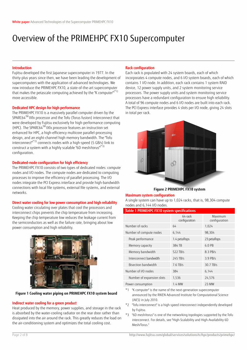
Introduction Fujitsu developed the first Japanese supercomputer in 1977. In the thirty-plus years since then, we have been leading the development of supercomputers with the application of advanced technologies. We now introduce the PRIMEHPC FX10, a state-of-the-art supercomputer that makes the petascale computing achieved by the "K computer"(*1) more accessible. Dedicated HPC design for high performance The PRIMEHPC FX10 is a massively parallel computer driven by the SPARC64TM IXfx processor and the Tofu (Torus fusion) interconnect that were developed by Fujitsu exclusively for high-performance computing (HPC). The SPARC64TM IXfx processor features an instruction set enhanced for HPC, a high-efficiency multicore parallel-processing design, and an eight-channel high memory bandwidth. The "Tofu interconnect"(*2) connects nodes with a high-speed (5 GB/s) link to construct a system with a highly scalable "6D mesh/torus"(*3) configuration. Dedicated-node configuration for high efficiency The PRIMEHPC FX10 consists of two types of dedicated nodes: compute nodes and I/O nodes. The compute nodes are dedicated to computing processes to improve the efficiency of parallel processing. The I/O nodes integrate the PCI Express interface and provide high-bandwidth connections with local file systems, external file systems, and external networks. Direct water cooling for low power consumption and high reliability Cooling water circulating over plates that cool the processors and interconnect chips prevents the chip temperature from increasing. Keeping the chip temperature low reduces the leakage current from the semiconductors as well as the failure rate, bringing about low power consumption and high reliability.
Indirect water cooling for a green product Heat produced by the memory, power supplies, and storage in the rack is absorbed by the water-cooling radiator on the rear door rather than dissipated into the air around the rack. This greatly reduces the load on the air-conditioning system and optimizes the total cooling cost.
Rack configuration Each rack is populated with 24 system boards, each of which incorporates 4 compute nodes, and 6 I/O system boards, each of which contains 1 I/O node. In addition, each rack contains 1 system RAID device, 12 power supply units, and 2 system monitoring service processors. The power supply units and system monitoring service processors have a redundant configuration to ensure high reliability. A total of 96 compute nodes and 6 I/O nodes are built into each rack. The PCI Express interface provides 4 slots per I/O node, giving 24 slots in total per rack.
Maximum system configuration A single system can have up to 1,024 racks, that is, 98,304 compute nodes and 6,144 I/O nodes.
64-rack configuration
Maximum configuration
Number of racks 64 1,024
Number of compute nodes 6,144 98,304
Peak performance 1.4 petaflops 23 petaflops
Memory capacity 384 TB 6.0 PB
Memory bandwidth 522 TB/s 8.3 PB/s
Interconnect bandwidth 245 TB/s 3.9 PB/s
Bisection bandwidth 7.6 TB/s 30.7 TB/s
Number of I/O nodes 384 6,144
Number of expansion slots 1,536 24,576
Power consumption 1.4 MW 23 MW
*1 "K computer" is the name of the next-generation supercomputer announced by the RIKEN Advanced Institute for Computational Science (AICS) in July 2010.
*2 "Tofu interconnect" is a high-speed interconnect independently developed by Fujitsu.
*3 "6D mesh/torus" is one of the networking topologies supported by the Tofu interconnect. For details, see "High-Scalability and High-Availability 6D Mesh/Torus."
Overview of the PRIMEHPC FX10 Supercomputer
Table 1 PRIMEHPC FX10 system specifications
Figure 2 PRIMEHPC FX10 system
Figure 1 Cooling water piping on PRIMEHPC FX10 system board
White paper Advanced Technologies of the Supercomputer PRIMEHPC FX10
Page 3 of 8 http://www.fujitsu.com/global/services/solutions/tc/hpc/products/primehpc/
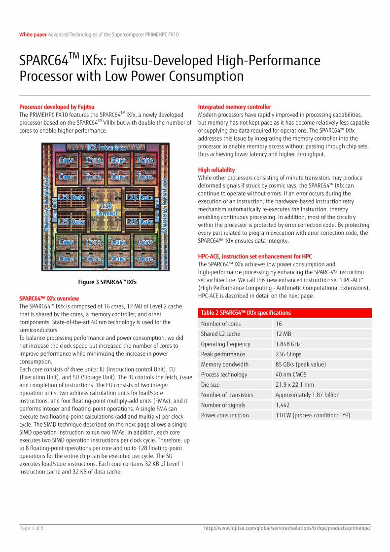
Processor developed by Fujitsu The PRIMEHPC FX10 features the SPARC64TM IXfx, a newly developed processor based on the SPARC64TM VIIIfx but with double the number of cores to enable higher performance.
SPARC64™ IXfx overview The SPARC64™ IXfx is composed of 16 cores, 12 MB of Level 2 cache that is shared by the cores, a memory controller, and other components. State-of-the-art 40 nm technology is used for the semiconductors. To balance processing performance and power consumption, we did not increase the clock speed but increased the number of cores to improve performance while minimizing the increase in power consumption. Each core consists of three units: IU (Instruction control Unit), EU (Execution Unit), and SU (Storage Unit). The IU controls the fetch, issue, and completion of instructions. The EU consists of two integer operation units, two address calculation units for load/store instructions, and four floating-point multiply-add units (FMAs), and it performs integer and floating-point operations. A single FMA can execute two floating-point calculations (add and multiply) per clock cycle. The SIMD technique described on the next page allows a single SIMD operation instruction to run two FMAs. In addition, each core executes two SIMD operation instructions per clock cycle. Therefore, up to 8 floating-point operations per core and up to 128 floating-point operations for the entire chip can be executed per cycle. The SU executes load/store instructions. Each core contains 32 KB of Level 1 instruction cache and 32 KB of data cache.
Integrated memory controller Modern processors have rapidly improved in processing capabilities, but memory has not kept pace as it has become relatively less capable of supplying the data required for operations. The SPARC64™ IXfx addresses this issue by integrating the memory controller into the processor to enable memory access without passing through chip sets, thus achieving lower latency and higher throughput. High reliability While other processors consisting of minute transistors may produce deformed signals if struck by cosmic rays, the SPARC64™ IXfx can continue to operate without errors. If an error occurs during the execution of an instruction, the hardware-based instruction retry mechanism automatically re-executes the instruction, thereby enabling continuous processing. In addition, most of the circuitry within the processor is protected by error correction code. By protecting every part related to program execution with error correction code, the SPARC64™ IXfx ensures data integrity. HPC-ACE, instruction set enhancement for HPC The SPARC64™ IXfx achieves low power consumption and high-performance processing by enhancing the SPARC-V9 instruction set architecture. We call this new enhanced instruction set "HPC-ACE" (High Performance Computing - Arithmetic Computational Extensions). HPC-ACE is described in detail on the next page.
Table 2 SPARC64™ IXfx specifications
Number of cores 16
Shared L2 cache 12 MB
Operating frequency 1.848 GHz
Peak performance 236 Gflops
Memory bandwidth 85 GB/s (peak value)
Process technology 40 nm CMOS
Die size 21.9 x 22.1 mm
Number of transistors Approximately 1.87 billion
Number of signals 1,442
Power consumption 110 W (process condition: TYP)
SPARC64TM IXfx: Fujitsu-Developed High-Performance Processor with Low Power Consumption
Figure 3 SPARC64TM IXfx
White paper Advanced Technologies of the Supercomputer PRIMEHPC FX10
Page 4 of 8 http://www.fujitsu.com/global/services/solutions/tc/hpc/products/primehpc/
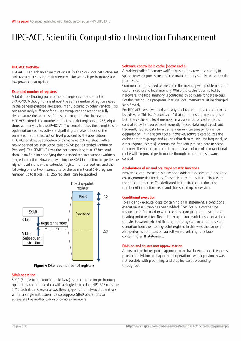
HPC-ACE overview HPC-ACE is an enhanced instruction set for the SPARC-V9 instruction set architecture. HPC-ACE simultaneously achieves high performance and low power consumption. Extended number of registers A total of 32 floating-point operation registers are used in the SPARC-V9. Although this is almost the same number of registers used in the general-purpose processors manufactured by other vendors, it is not necessarily sufficient for a supercomputer application to fully demonstrate the abilities of the supercomputer. For this reason, HPC-ACE extends the number of floating-point registers to 256, eight times as many as in the SPARC-V9. The compiler uses these registers for optimization such as software pipelining to make full use of the parallelism at the instruction level provided by the application. HPC-ACE enables specification of as many as 256 registers, with a newly defined pre-instruction called SXAR (Set eXtended Arithmetic Register). The SPARC-V9 fixes the instruction length at 32 bits, and there is no field for specifying the extended register number within a single instruction. However, by using the SXAR instruction to specify the higher-level 3 bits of the extended register number portion, and the following one or two instructions for the conventional 5-bit register number, up to 8 bits (i.e., 256 registers) can be specified.
SIMD operation SIMD (Single Instruction Multiple Data) is a technique for performing operations on multiple data with a single instruction. HPC-ACE uses the SIMD technique to execute two floating-point multiply-add operations within a single instruction. It also supports SIMD operations to accelerate the multiplication of complex numbers.
Software-controllable cache (sector cache) A problem called "memory wall" relates to the growing disparity in speed between processors and the main memory supplying data to the processors. Common methods used to overcome the memory wall problem are the use of a cache and local memory. While the cache is controlled by hardware, the local memory is controlled by software for data access. For this reason, the programs that use local memory must be changed significantly. For HPC-ACE, we developed a new type of cache that can be controlled by software. This is a "sector cache" that combines the advantages of both the cache and local memory. In a conventional cache that is controlled by hardware, less-frequently reused data might push out frequently reused data from cache memory, causing performance degradation. In the sector cache, however, software categorizes the cache data into groups and assigns that data reused less frequently to other regions (sectors) to retain the frequently reused data in cache memory. The sector cache combines the ease of use of a conventional cache with improved performance through on-demand software control. Acceleration of sin and cos trigonometric functions New dedicated instructions have been added to accelerate the sin and cos trigonometric functions. Conventionally, many instructions were used in combination. The dedicated instructions can reduce the number of instructions used and thus speed up processing. Conditional execution To efficiently execute loops containing an IF statement, a conditional execution instruction has been added. Specifically, a comparison instruction is first used to write the condition judgment result into a floating-point register. Next, the comparison result is used for a data transfer between selected floating-point registers or a memory store operation from the floating-point register. In this way, the compiler also performs optimization via software pipelining for a loop containing an IF statement. Division and square root approximation An instruction for reciprocal approximation has been added. It enables pipelining division and square root operations, which previously was not possible with pipelining, and thus increases processing throughput.
HPC-ACE, Scientific Computation Instruction Enhancement
Figure 4 Extended number of registers
White paper Advanced Technologies of the Supercomputer PRIMEHPC FX10
Page 5 of 8 http://www.fujitsu.com/global/services/solutions/tc/hpc/products/primehpc/
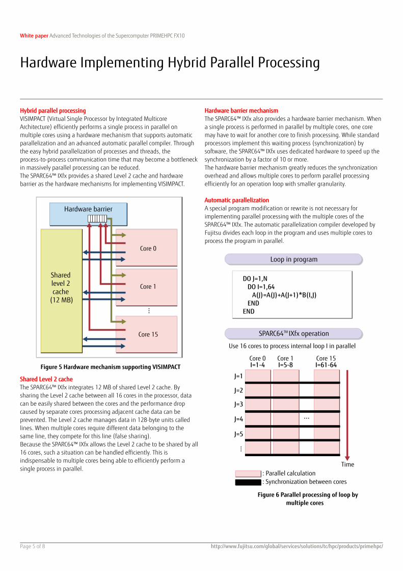
Hybrid parallel processing VISIMPACT (Virtual Single Processor by Integrated Multicore Architecture) efficiently performs a single process in parallel on multiple cores using a hardware mechanism that supports automatic parallelization and an advanced automatic parallel compiler. Through the easy hybrid parallelization of processes and threads, the process-to-process communication time that may become a bottleneck in massively parallel processing can be reduced. The SPARC64™ IXfx provides a shared Level 2 cache and hardware barrier as the hardware mechanisms for implementing VISIMPACT.
...
Shared Level 2 cache The SPARC64™ IXfx integrates 12 MB of shared Level 2 cache. By sharing the Level 2 cache between all 16 cores in the processor, data can be easily shared between the cores and the performance drop caused by separate cores processing adjacent cache data can be prevented. The Level 2 cache manages data in 128-byte units called lines. When multiple cores require different data belonging to the same line, they compete for this line (false sharing). Because the SPARC64™ IXfx allows the Level 2 cache to be shared by all 16 cores, such a situation can be handled efficiently. This is indispensable to multiple cores being able to efficiently perform a single process in parallel.
Hardware barrier mechanism The SPARC64™ IXfx also provides a hardware barrier mechanism. When a single process is performed in parallel by multiple cores, one core may have to wait for another core to finish processing. While standard processors implement this waiting process (synchronization) by software, the SPARC64™ IXfx uses dedicated hardware to speed up the synchronization by a factor of 10 or more. The hardware barrier mechanism greatly reduces the synchronization overhead and allows multiple cores to perform parallel processing efficiently for an operation loop with smaller granularity. Automatic parallelization A special program modification or rewrite is not necessary for implementing parallel processing with the multiple cores of the SPARC64™ IXfx. The automatic parallelization compiler developed by Fujitsu divides each loop in the program and uses multiple cores to process the program in parallel.
Hardware Implementing Hybrid Parallel Processing
Figure 6 Parallel processing of loop by multiple cores
Figure 5 Hardware mechanism supporting VISIMPACT
White paper Advanced Technologies of the Supercomputer PRIMEHPC FX10
Page 6 of 8 http://www.fujitsu.com/global/services/solutions/tc/hpc/products/primehpc/
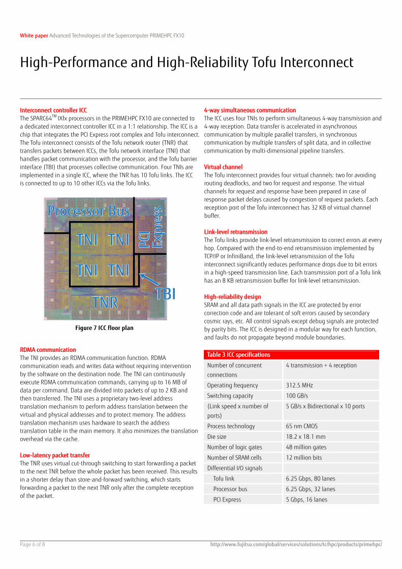
Interconnect controller ICC The SPARC64TM IXfx processors in the PRIMEHPC FX10 are connected to a dedicated interconnect controller ICC in a 1:1 relationship. The ICC is a chip that integrates the PCI Express root complex and Tofu interconnect. The Tofu interconnect consists of the Tofu network router (TNR) that transfers packets between ICCs, the Tofu network interface (TNI) that handles packet communication with the processor, and the Tofu barrier interface (TBI) that processes collective communication. Four TNIs are implemented in a single ICC, where the TNR has 10 Tofu links. The ICC is connected to up to 10 other ICCs via the Tofu links.
RDMA communication The TNI provides an RDMA communication function. RDMA communication reads and writes data without requiring intervention by the software on the destination node. The TNI can continuously execute RDMA communication commands, carrying up to 16 MB of data per command. Data are divided into packets of up to 2 KB and then transferred. The TNI uses a proprietary two-level address translation mechanism to perform address translation between the virtual and physical addresses and to protect memory. The address translation mechanism uses hardware to search the address translation table in the main memory. It also minimizes the translation overhead via the cache. Low-latency packet transfer The TNR uses virtual cut-through switching to start forwarding a packet to the next TNR before the whole packet has been received. This results in a shorter delay than store-and-forward switching, which starts forwarding a packet to the next TNR only after the complete reception of the packet.
4-way simultaneous communication The ICC uses four TNIs to perform simultaneous 4-way transmission and 4-way reception. Data transfer is accelerated in asynchronous communication by multiple parallel transfers, in synchronous communication by multiple transfers of split data, and in collective communication by multi-dimensional pipeline transfers. Virtual channel The Tofu interconnect provides four virtual channels: two for avoiding routing deadlocks, and two for request and response. The virtual channels for request and response have been prepared in case of response packet delays caused by congestion of request packets. Each reception port of the Tofu interconnect has 32 KB of virtual channel buffer. Link-level retransmission The Tofu links provide link-level retransmission to correct errors at every hop. Compared with the end-to-end retransmission implemented by TCP/IP or InfiniBand, the link-level retransmission of the Tofu interconnect significantly reduces performance drops due to bit errors in a high-speed transmission line. Each transmission port of a Tofu link has an 8 KB retransmission buffer for link-level retransmission. High-reliability design SRAM and all data path signals in the ICC are protected by error correction code and are tolerant of soft errors caused by secondary cosmic rays, etc. All control signals except debug signals are protected by parity bits. The ICC is designed in a modular way for each function, and faults do not propagate beyond module boundaries.
Table 3 ICC specifications
Number of concurrent
connections
4 transmission + 4 reception
Operating frequency 312.5 MHz
Switching capacity 100 GB/s
(Link speed x number of
ports)
5 GB/s x Bidirectional x 10 ports
Process technology 65 nm CMOS
Die size 18.2 x 18.1 mm
Number of logic gates 48 million gates
Number of SRAM cells 12 million bits
Differential I/O signals
Tofu link 6.25 Gbps, 80 lanes
Processor bus 6.25 Gbps, 32 lanes
PCI Express 5 Gbps, 16 lanes
High-Performance and High-Reliability Tofu Interconnect
Figure 7 ICC floor plan
White paper Advanced Technologies of the Supercomputer PRIMEHPC FX10
Page 7 of 8 http://www.fujitsu.com/global/services/solutions/tc/hpc/products/primehpc/
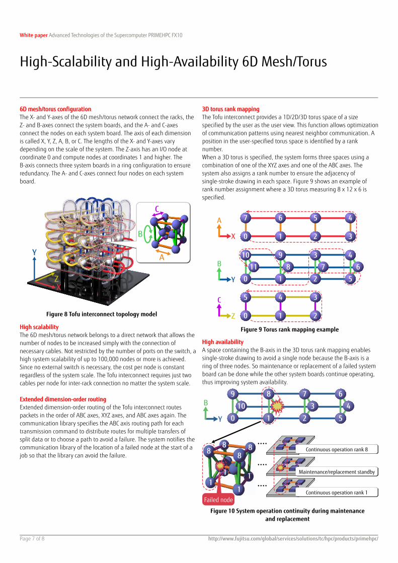
6D mesh/torus configuration The X- and Y-axes of the 6D mesh/torus network connect the racks, the Z- and B-axes connect the system boards, and the A- and C-axes connect the nodes on each system board. The axis of each dimension is called X, Y, Z, A, B, or C. The lengths of the X- and Y-axes vary depending on the scale of the system. The Z-axis has an I/O node at coordinate 0 and compute nodes at coordinates 1 and higher. The B-axis connects three system boards in a ring configuration to ensure redundancy. The A- and C-axes connect four nodes on each system board.
High scalability The 6D mesh/torus network belongs to a direct network that allows the number of nodes to be increased simply with the connection of necessary cables. Not restricted by the number of ports on the switch, a high system scalability of up to 100,000 nodes or more is achieved. Since no external switch is necessary, the cost per node is constant regardless of the system scale. The Tofu interconnect requires just two cables per node for inter-rack connection no matter the system scale. Extended dimension-order routing Extended dimension-order routing of the Tofu interconnect routes packets in the order of ABC axes, XYZ axes, and ABC axes again. The communication library specifies the ABC axis routing path for each transmission command to distribute routes for multiple transfers of split data or to choose a path to avoid a failure. The system notifies the communication library of the location of a failed node at the start of a job so that the library can avoid the failure.
3D torus rank mapping The Tofu interconnect provides a 1D/2D/3D torus space of a size specified by the user as the user view. This function allows optimization of communication patterns using nearest neighbor communication. A position in the user-specified torus space is identified by a rank number. When a 3D torus is specified, the system forms three spaces using a combination of one of the XYZ axes and one of the ABC axes. The system also assigns a rank number to ensure the adjacency of single-stroke drawing in each space. Figure 9 shows an example of rank number assignment where a 3D torus measuring 8 x 12 x 6 is specified.
High availability A space containing the B-axis in the 3D torus rank mapping enables single-stroke drawing to avoid a single node because the B-axis is a ring of three nodes. So maintenance or replacement of a failed system board can be done while the other system boards continue operating, thus improving system availability.
High-Scalability and High-Availability 6D Mesh/Torus
Figure 9 Torus rank mapping example
Figure 8 Tofu interconnect topology model
Figure 10 System operation continuity during maintenance and replacement
White paper Advanced Technologies of the Supercomputer PRIMEHPC FX10
Page 8 of 8 http://www.fujitsu.com/global/services/solutions/tc/hpc/products/primehpc/
Tofu barrier interface Collective communication processing is achieved with packet reception, calculations, and packet transmission repeated by each node. The Tofu barrier interface (TBI) is hardware for handling collective communication on behalf of the processor to accelerate collective communication. The TBI has 64 barrier gates for receiving packets, performing calculations, and transmitting packets. Each barrier gate has a reception buffer for a single packet. Multiple packet transmission and reception by multiple barrier gates is implemented with a range of communication algorithms. Supported collective communication types The TBI supports two types of collective communication: Barrier and AllReduce. AllReduce can also be used as Broadcast or Reduce. To perform AllReduce collective communication, the TBI stores the operation type and single-element data in the barrier packet. A 64-bit integer and floating-point number represented in the Tofu specific format can be stored. The 64-bit integer can be specified for the AND, OR, XOR, MAX, and SUM operations, and the unique floating-point number for the SUM operation. The unique floating-point number is designed so that equivalent results can be obtained with low latency regardless of which communication algorithm is used. The format is a low-overhead unique radix representation of 280 semi-fixed points, which can be mutually converted with the IEEE 754 floating-point numbers. To prevent SUM operation results from changing depending on the calculation order, SUM is performed by a proprietary algorithm using two 154-bit significands. Various communication algorithms Barrier gates can be combined in different ways to implement a range of communication algorithms. The communication library uses a different communication algorithm depending on the purpose. The Recursive Doubling algorithm is ideal for those cases where a short delay is preferable because it completes AllReduce for N nodes in log2N steps. However, every node requires a reception buffer for log2N steps, and many barrier gates are consumed. The Ring algorithm requires 2N steps to complete AllReduce for N nodes, but the required number of barrier gates can be reduced because each node only uses a reception buffer for two steps. The Tree algorithm consists of reduction and broadcast trees, and
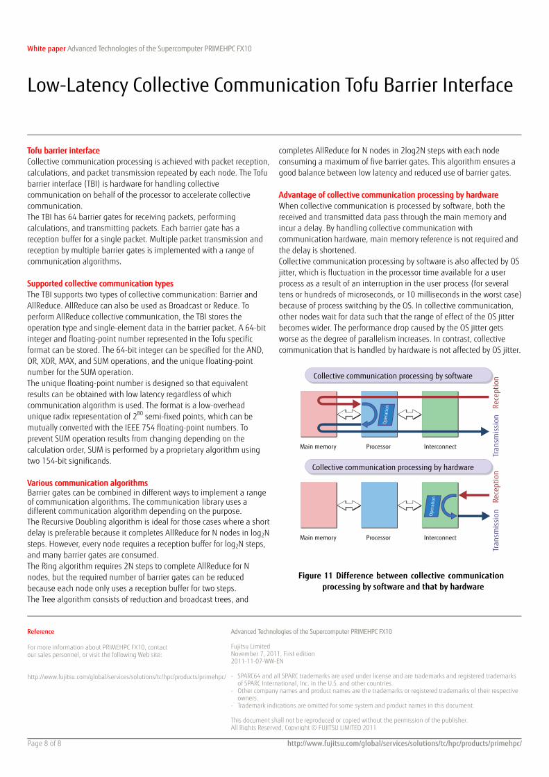
completes AllReduce for N nodes in 2log2N steps with each node consuming a maximum of five barrier gates. This algorithm ensures a good balance between low latency and reduced use of barrier gates. Advantage of collective communication processing by hardware When collective communication is processed by software, both the received and transmitted data pass through the main memory and incur a delay. By handling collective communication with communication hardware, main memory reference is not required and the delay is shortened. Collective communication processing by software is also affected by OS jitter, which is fluctuation in the processor time available for a user process as a result of an interruption in the user process (for several tens or hundreds of microseconds, or 10 milliseconds in the worst case) because of process switching by the OS. In collective communication, other nodes wait for data such that the range of effect of the OS jitter becomes wider. The performance drop caused by the OS jitter gets worse as the degree of parallelism increases. In contrast, collective communication that is handled by hardware is not affected by OS jitter.
Low-Latency Collective Communication Tofu Barrier Interface
Reference For more information about PRIMEHPC FX10, contact our sales personnel, or visit the following Web site: http://www.fujitsu.com/global/services/solutions/tc/hpc/products/primehpc/
Advanced Technologies of the Supercomputer PRIMEHPC FX10 Fujitsu Limited November 7, 2011, First edition 2011-11-07-WW-EN - SPARC64 and all SPARC trademarks are used under license and are trademarks and registered trademarks
of SPARC International, Inc. in the U.S. and other countries. - Other company names and product names are the trademarks or registered trademarks of their respective
owners. - Trademark indications are omitted for some system and product names in this document. This document shall not be reproduced or copied without the permission of the publisher. All Rights Reserved, Copyright © FUJITSU LIMITED 2011
Figure 11 Difference between collective communication processing by software and that by hardware