Embed Size (px)
Citation preview
Advances in Cold Cathode Physicsand Technology
JOHN A. NATION, FELLOW, IEEE, LEVI SCHACHTER, MEMBER, IEEE,FREDERICK M. MAKO, MEMBER, IEEE, L. K. LEN, MEMBER, IEEE, WILLIAM PETER, MEMBER, IEEE,CHA-MEI TANG, SENIOR MEMBER, IEEE, AND TRIVENI SRINIVASAN-RAO
Invited Paper
We review recent progress in the physics and technology ofcold cathode electron emitters. The characteristics of emissionfrom field emitter arrays, photocathodes, and ferroelectrics arepresented, together with a summary of the understanding of thephysics involved. The paper concludes with a description of L-bandmicropulse gun, based on secondary emission in an RF cavity.Emphasis is placed on cathode development for electron guns todrive microwave tubes and RF accelerators.
Keywords—Cathodes, electron beams, electron emission, fer-roelectric materials, microwave tubes, linear accelerators, photoelectricity.
I. INTRODUCTION
In this paper we address the topic of new approaches tothe production of high brightness electron beams. For manyyears, vacuum electronic devices have used thermioniccathodes as the preferred source. Cathode currents of up toseveral hundred amperes have been produced with durationsof a few microseconds, usually at current densities oforder 10 A/cm and repetition rates of about 100 Hz. Atthese high current levels, substantial beam compression isneeded for microwave sources at frequencies in excess of
Manuscript received November 6, 1997; revised January 22, 1999.This work was supported in part by the United States Department ofEnergy under the SBIR Program. The work of J. A. Nation and L.Schachter was supported by the United States Department of Energy,the AFOSR under the MURI Program, and by the Bi-National ScienceFoundation United States–Israel. The work of C.-M. Tang was supportedby the National Institute of Standards and Technology, Defense AdvancedResearch Projects Agency, and by the Air Force Office of ScientificResearch. The work of T. Srinivasan-Rao was supported by the UnitedStates Department of Energy.
J. A. Nation is with the School of Electrical Engineering and Laboratoryof Plasma Studies, Cornell University, Ithaca, NY 14583 USA.
L. Schachter is with the Electrical Engineering Department, Technion,Haifa 32000 Israel.
F. M. Mako, L. K. Len, and W. Peter are with FM Technologies, Inc.,Fairfax, VA 22032 USA.
C.-M. Tang is with Creatv MicroTech, Inc., Potomac, MD 20854 USA.T. Srinivasan-Rao is with Brookhaven National Laboratory, Upton, NY
11973 USA.Publisher Item Identifier S 0018-9219(99)03058-3.
a gigahertz. Cathode lifetimes, in this mode of operation,extend to many years. Similarly, continuous operating mi-crowave devices, which operate at power levels in the Wattto multikilowatt regime, require cathodes with comparablemultiyear life. Recent advances have been driven by needsfor ultrahigh-power devices with higher available emissioncurrent densities, and by the desire to directly modulate theelectron beam at the source. In addition, direct modulationof the beam to produce a train of short pulses is of interestfor cathode use as a buncher for RF linacs. We shall addressboth of these topics in the following sections.
In Section II, we review recent developments in fieldemission and direct modulation of electron beams usingfield emission arrays (FEA’s). Field-emission cathodes havebeen fabricated using a variety of materials and by a varietyof methods. Single tips with a radius of curvature about 60nm to 90 nm have been used to generate current densitiesof more than 10 A/cm , and arrays of tips have generatedcurrent densities of 10 to 2400 A/cm, which exceed currentdensities available from thermionic cathodes. Emissionfrom gated FEA’s can be initiated by the application ofgate voltages of less than 100 V. Among the advantagesenvisioned for FEA’s is the ability to address and controlthe emission spatially and to directly modulate the emissioncurrent. Normalized beam brightness from single tips withtotal currents of 10 mA is estimated to be on the orderof 10 A/(m -steradian), about a factor of a hundred toa thousand times better than thermionic cathodes. Studiesare being carried out to measure the beam emittance fromthese tips. The emittance from an array of tips is, however,poor without integrated lenses on each tip.
Two traveling-wave tubes (TWT’s) have been success-fully operated by NEC Corporation using lateral resistor-stabilized FEA’s and arc-resistant FEA’s. The TWT drivenby the arc-resistant FEA’s achieved 5000 h of operation.The test was terminated by a cause other than arc failure.Direct modulation of the emitted beam can improve the
0018–9219/99$10.00 1999 IEEE
PROCEEDINGS OF THE IEEE, VOL. 87, NO. 5, MAY 1999 865
efficiency and reduce the size of the microwave source.A method of direct beam modulation is to modulate thevoltage of the gate electrode of the FEA. Gate modulationis complicated by the large input capacitance caused bythe small distance between the gate and the substrate.Nonetheless, several groups have demonstrated emissionmodulation on top of dc current at frequencies of up to10 GHz. This device offers a compact and, potentially,highly efficient microwave source. In this section of thepaper, we summarize emission data from single tips andarrays of emitters and discuss issues pertinent to tube ap-plications, including beam emittance and brightness, energyspread, uniformity and stability, reliability and frequencyof emission modulation.
Field-emitter cathodes are envisioned to be capable ofimproving the performance of many low- and medium-power devices and enabling new devices without decreasingthe cathode lifetime.
In Section III, we discuss recent developments in pho-toemission. Recent advances in short pulse duration high-power lasers allow the generation of trains of electronbunches with lengths of less than 30m, about one-thirtiethof a cycle at 10 GHz, each containing tens of nC charge. Asin the case of the FEA, the temporal and spatial distributionof the emitted charge can be controlled, in this case bycontrol of the incident laser pulses. Much of the focusof this work has centered on the production of a singlepulse or limited extent trains of pulses for injection intoL- and S-band linacs. An example of the use of laser-driven photocathodes for RF generation may be found inthe CLIC (CERN linear collider) test accelerator. In thisapplication, a high-energy electron beam is generated usinga photocathode and postaccelerated to an energy of about50 MeV. The test facility uses a CsTe cathode irradiatedwith a YLF laser at 262 nm to produce10 ps pulses with
30 nC of charge/bunch and at a modulation frequency of3 GHz. The bunched beam is accelerated and then used toexcite 30-GHz waves that are coupled through a transferstructure to a test accelerator. The use of beams bunched atsubharmonics of the required frequency may also providea useful option for high-power, high-frequency microwavegeneration. In this section of the paper we review progressin metallic and semiconductor photocathodes with specialreference to the properties of the cathodes used.
Section IV discusses a relatively new electron source, aferroelectric cathode. Free charge exists on the surface ofa pre-poled ferroelectric that screens the extremely largeelectrostatic fields due to the material polarization fromthe surrounding electron gun vacuum. The application ofa rapidly changing electric field across the ferroelectricmaterial may modify the amount of surface charge requiredto produce the electrostatic screening. Surplus charge isemitted into the gun and may be used for the productionof pulsed electron beams. Depending on the polarity of thetrigger pulse used to initiate emission, it is also possible togenerate the electron beam from the metallic grid on thefront surface of the ferroelectric. In this configuration, theceramic acts as a high dielectric constant, albeit nonlinear
material, which serves to enhance the field causing theemission at the triple points on the front surface of theceramic. In this mode of use the emission is similarto that found in FEA arrays where the application ofthe emission trigger pulse to the gate electrode in theFEA is replaced by pulsing of the rear surface of theemitter. Unlike the previous two topics, relatively littlework has been done to date on beam modulation, and workhas focused on the understanding of the physics of theemission process. Experiments have been carried out withemission initiated by changing the material (e.g., PLZT)from an antiferroelectric to a ferroelectric state, and inother cases by cycling a ferroelectric material (e.g., PZT)around a minor hysteresis loop. In both cases the role ofthe material polarization on the screening charge is crucialin determining the emission. Beam current densities of upto about 1 kA/cm and currents of several hundred ampereshave been extracted in10’s of nanosecond to microsecondpulses. The relative ease of generation of electron beamcurrent makes this source an attractive option for ultrahigh-power microwave sources. In this section of the paperwe report experimental data and theoretical models of thepresent understanding of the physics of the emission. Inaddition, measurements of such parameters as the beamemittance, sensitivity to vacuum, repetition rate capability,and photoemission characteristics are described.
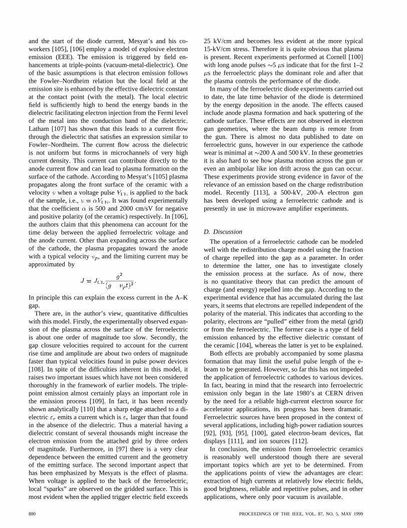
Section V describes an interesting new concept employ-ing secondary emission of electrons for the generationof trains of short bunches of electrons for injection intoRF accelerators or microwave devices. The concept uti-lizes secondary emission and multipacting of electrons togenerate naturally bunched electron beams with the useof microwave fields. One wall of an RF cavity is madepartially transparent to electrons but opaque to an input RFelectric field in order to extract the beam. Self-consistentanalytic theory and 2-1/2-dimensional (2-1/2-D), fully rel-ativistic, electromagnetic particle-in-cell (PIC) simulationsshow that natural bunching occurs and one bunch is emittedfor each RF period. The paper describes the principles of thesecondary emission bunch beam generator. It is shown thatthe bunch length is adjustable from 2–10% of the RF periodand the current density scales with frequency cubed. Thenatural bunching provides high-current densities (0.005–10kA/cm ), short-pulse (1–100 ps) bunches, and low normal-ized transverse emittance (2–3 mm mrad with 10electronsper bunch at extraction energies in the range 20 keV–100keV, respectively). As in the case of photoemitters, thebunched beam may be post accelerated using a linac atthe bunch frequency, electrostatically or inductively, forinjection into a tuned system for the generation of high-power RF signals.
This section concludes with a description of a proof-of-principle experiment at 1.3 GHz that shows reproduciblebunches of 50–70-ps pulse length with a current density of20 A/cm in agreement with theoretical prediction. Workis presently in progress to attempt to scale this device to S-and X-band. The long trains of electron bunches make thisdevice particularly suited for use as an injector in a linac.
866 PROCEEDINGS OF THE IEEE, VOL. 87, NO. 5, MAY 1999
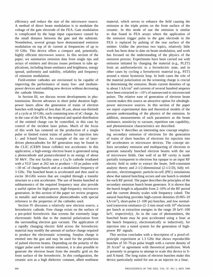
Fig. 1. A schematic diagram of Spindt type gated field-emitter array.
In Section VI, we briefly outline other new cold cathodeelectron sources which have been proposed. In addition,recent work has been described on oxide cathodes whichoffer the potential of emission at current densities of 50–100A/cm .
II. FIELD EMISSION CATHODES
A. Introduction
The use of field-emission cathodes is a practical methodfor delivering a high current density from field emissioncathodes without substantial thermal, optical or electricalpower. FEA’s, with their high current densities and fastturn on, have been envisioned to be capable of improvingthe performance of many devices such as microwave am-plifiers and enabling new devices, e.g., field emission flatpanel displays and fast power switches, without decreasingcathode lifetime. This goal is beginning to be realizedfor displays and first results have been obtained with mi-crowave tubes. Two proof-of-concept X-band miniaturizedtraveling-wave tubes using Spindt-type FEA’s are the firstto demonstrate microwave amplification with good cathodelifetime [1]–[4]. Extensive research has been conductedto develop wideband microwave amplifiers with improvedhigh efficiency and reduced device size by using FEAcathodes to prebunch the electron beam [5]–[15].
An electron extraction electrode, the gate, is typically 0.5m or less from a sharp emitter tip or edge. A schematic of
a gated, conical, FEA fabricated by Spindt of SRI is shownin Fig. 1. Spindt was the first to successfully make thegated FEA’s using microfabrication technology [16]. Soonafter, Gray of Naval Research Laboratory demonstrated theoperation of silicon field emitter’s [17].
Field emitters have the following unique properties.
• Emission current density from single tips can be muchlarger than 10 A/cm . A current of up to 49 mA wasobtained from a single tip of approximately 90-nmradius of curvature in a pulsed mode [18]–[19]. Thetip approximates a point source.
• Emission current densities up to 2400 A/cmhave beenobserved from arrays of field emitters [6], [12]–[13].
• Emission can be turned on with low gate voltages( 100 V). The field emitter cathode can be compactand simple to operate.
• Emission can be temporally modulated at high frequen-cies. Frequency modulation by gate voltage has beendemonstrated up to 10 GHz [5]–[11].
• Emission can be spatially addressed in the– plane.• Electron emission is cold field emission. The power
required to produce the emission is low. This is animportant factor for compact devices.
• A large number of organizations worldwide haveshown that they can reliably fabricate and operateFEA’s using a variety of techniques and materials.Field-emission tips and edges have been successfullyfabricated from silicon, gallium arsenide, zirconiumcarbide, hafnium carbide, titanium, niobium, tungsten,lithium, diamond, carbon nanotubes, and many othermaterials. There have been significant advances inthe fabrication techniques, particularly in precisionpatterning of arrays of small holes over large areas atlow cost, and in exploiting a wide variety of depositionand etching techniques.
• For low current density and low duty cycle applica-tions such as field-emission flat panel displays, therehave been significant advances in the last few years[20]–[23]. Products are on the market and many com-panies have prototypes. For high current density appli-cations, more experience is needed with processing andoperation in a vacuum tube environment. In this sectionwe will describe the special characteristics of micro-field-emission sources quantitatively. We shall addressthe following issues with emphasis on high currentdensity: physics of field emission; single tip versusarrays of tips; beam brightness and beam collimation;emission uniformity and stabilization; energy spread;high frequency density modulation; life expectancy;and microwave tube applications.
B. Physics of Field Emission and theFowler–Nordheim Equation
Within a metal, an electron current density of roughly10 A/cm impinges on the inner surface. Only a smallfraction of this current escapes from the metal due to thesurface-tunneling barrier as shown in Fig. 2 [24]. Thissurface tunneling barrier exceeds the Fermi energyby the value of the work function , which is about 2–5eV at zero applied field. This barrier can be modified bythe application of an electric field that decreases thepotential energy by the amount outside the metal,
NATION et al.: ADVANCES IN COLD CATHODE PHYSICS AND TECHNOLOGY 867
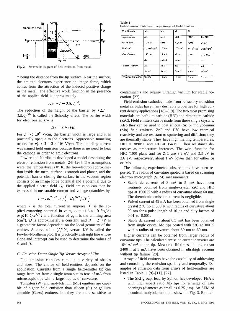
Fig. 2. Schematic diagram of field emission from metal.
being the distance from the tip surface. Near the surface,the emitted electrons experience an image force, whichcomes from the attraction of the induced positive chargein the metal. The effective work function in the presenceof the applied field is approximately
The reduction of the height of the barrier byis called the Schottky effect. The barrier width
for electrons at is
For V/cm, the barrier width is large and it ispractically opaque to the electrons. Appreciable tunnelingoccurs for V/cm. The tunneling currentwas named field emission because there is no need to heatthe cathode in order to emit electrons.
Fowler and Nordheim developed a model describing theelectron emission from metals [24]–[26]. The assumptionswere: the temperature is 0K, the free-electron approxima-tion inside the metal surface is smooth and planar, and thepotential barrier closing the surface in the vacuum regionconsists of an image force potential and a potential due tothe applied electric field . Field emission can then beexpressed in measurable current and voltage quantities by
where is the total current in amperes, is the ap-plied extracting potential in volts,
is a function of is the emitting area(cm ), is approximately a constant, and isa geometric factor dependent on the local geometry of theemitter. A curve of ln versus 1/V is called theFowler–Nordheim plot. It is practically a straight line whoseslope and intercept can be used to determine the values of
and .
C. Emission Data: Single Tip Versus Arrays of Tips
Field-emission cathodes come in a variety of shapesand sizes. The choice of field-emitters depends on theapplication. Currents from a single field-emitter tip canrange from pA from a single atom site to tens of mA frommicroscopic tips with a larger radius of curvature.
Tungsten (W) and molybdenum (Mo) emitters are capa-ble of higher field emission than silicon (Si) or galliumarsenide (GaAs) emitters, but they are more sensitive to
Table 1Field-Emission Data from Large Arrays of Field Emitters
contaminants and require ultrahigh vacuum for stable op-eration [27].
Field-emission cathodes made from refractory transitionmetal carbides have many desirable properties for high cur-rent density applications [18]–[19]. The two most promisingmaterials are hafnium carbide (HfC) and zirconium carbide(ZrC). Field emitters can be made from these single crystals.Also they can be used to coat silicon (Si) or molybdenum(Mo) field emitters. ZrC and HfC have low chemicalreactivity and are resistant to sputtering and diffusion; theyare thermally stable. They have high melting temperatures:HfC at 3890 C and ZrC at 3540C. Their resistance de-creases as temperature increases. The work function forHfC (100) plane and for ZrC are 3.2 eV and 3.3 eV to3.6 eV, respectively, about 1 eV lower than for either Sior Mo.
The following experimental observations have been re-ported. The radius of curvature quoted is based on scanningelectron micrograph (SEM) measurements.
• Stable dc currents of 3 mA to 5 mA have beenroutinely obtained from single-crystal ZrC and HfCtips at 1500 K with a radius of curvature about 60 nm.The thermionic emission current is negligible.
• Pulsed current of 49 mA has been obtained from singlecrystal ZrC tip at 300 K with radius of curvature about90 nm for a pulse length of 10s and duty factors of0.01 to 0.001.
• Stable dc current of about 0.5 mA has been obtainedfrom single crystal Mo tips coated with ZrC at 300 Kwith a radius of curvature about 30 nm to 60 nm.
Higher currents can be obtained from larger radius ofcurvature tips. The calculated emission current densities are10 A/cm at the tip. Measured lifetimes of longer than2400 h at 5 mA have been obtained in ultrahigh vacuumwithout tip failure [28].
Arrays of field emitters have the capability of addressingand controlling the emission spatially and temporally. Ex-amples of emission data from arrays of field-emitters arelisted in Table 1 [9]–[11], [27].
• The SRI group, lead by Spindt, has developed FEA’swith high aspect ratio Mo tips for a range of gateopenings (diameter as small as 0.25m). An SEM ofa conical, molybdenum tip is shown in Fig. 3. Emitter-
868 PROCEEDINGS OF THE IEEE, VOL. 87, NO. 5, MAY 1999
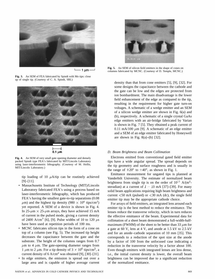
Fig. 3. An SEM of FEA fabricated by Spindt with Mo tips: closeup of single tip. (Courtesy of C. A. Spindt, SRI.)
Fig. 4. An SEM of very small gate opening diameter and denselypacked Spindt type FEA’s fabricated by MIT/Lincoln Laboratoryusing laser-interferometric lithography. (Courtesy of M. Hollis,MIT/Lincoln Laboratory.)
tip loading of 10 A/tip can be routinely achieved[9]–[11].
• Massachusetts Institute of Technology (MIT)/LincolnLaboratory fabricated FEA’s using a process based onlaser-interferometric lithography, which has producedFEA’s having the smallest gate-to-tip separations (0.08
m) and the highest tip density (980 10 tips/cm )yet reported. A SEM of a device is shown in Fig. 4.In 25- m 25- m arrays, they have achieved 15 mAof current in the pulsed mode, giving a current densityof 2400 A/cm [6], [9]. Pulse widths of 10 to 120 shave been used at repetition periods of 100 ms.
• MCNC fabricates silicon tips in the form of a cone ontop of a column (see Fig. 5). The increased tip heightdecreases the capacitance between the gate and thesubstrate. The height of the columns ranges from 0.7
m to 4 m. The gate-opening diameter ranges from1 m to 2 m. For a tip density of 3 10 tips/cm , acurrent density of 6 A/cmwas obtained [9], [30]–[31].
• In edge emitters, the emission is spread out over alarge area and is capable of higher average current
Fig. 5. An SEM of silicon field emitters in the shape of cones oncolumns fabricated by MCNC. (Courtesy of D. Temple, MCNC.)
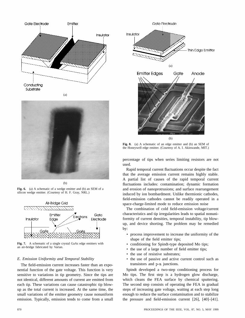
density than that from cone emitters [5], [9], [32]. Forsome designs the capacitance between the cathode andthe gate can be low and the edges are protected fromion bombardment. The main disadvantage is the lowerfield enhancement of the edge as compared to the tip,resulting in the requirement for higher gate turn-onvoltages. A schematic of a wedge emitter and an SEMof a silicon wedge emitter are shown in Fig. 6(a) and(b), respectively. A schematic of a single crystal GaAsedge emitters with an air-bridge fabricated by Varianis shown in Fig. 7 [5]. They obtained a peak current of0.11 mA/100 m [9]. A schematic of an edge emitterand a SEM of an edge emitter fabricated by Honeywellare shown in Fig. 8(a)–(b) [32].
D. Beam Brightness and Beam Collimation
Electrons emitted from conventional gated field emittertips have a wide angular spread. The spread depends onthe tip geometry and surface roughness and is usually inthe range of 20 to 40 , as shown in Fig. 1.
Emittance measurement for ungated tips is planned atVanderbilt University. The estimate of normalized beambrightness from single tip is on the order of 10A/(m -steradian) at a current of mA [37]–[39]. For manysolid beam applications requiring high beam brightness andcurrent 50 mA (pulsed) or 30 mA (dc), the single fieldemitter tip may be the appropriate cathode choice.
For arrays of field emitters, an integrated lens around eachemitter tip is the best method to reduce the emittance. Thelenses reduce the transverse velocity, which in turn reducesthe effective emittance of the beam. Experimental data forcollimation of a sheet beam demonstrated a full-width-half-maximum (FWHM) of the sheet to be better than 33m fora gate at 60 V, lens at 4 V, and anode at 1.5 kV to 2.5 kVand for an anode–cathode separation of 10 mm [35]. Thiscorresponds to a reduction of the spot size at the anodeby a factor of 100 from the unfocused case indicating areduction in the transverse velocity by a factor about 100.Even though emitters with integrated lenses are less dense,i.e., the initial current density is lower, the overall beambrightness can be improved due to a significant reductionof the normalized emittance.
NATION et al.: ADVANCES IN COLD CATHODE PHYSICS AND TECHNOLOGY 869
(a)
(b)
Fig. 6. (a) A schematic of a wedge emitter and (b) an SEM of asilicon wedge emitter. (Courtesy of H. F. Gray, NRL.)
Fig. 7. A schematic of a single crystal GaAs edge emitters withan air-bridge fabricated by Varian.
E. Emission Uniformity and Temporal Stability
The field-emission current increases faster than an expo-nential function of the gate voltage. This function is verysensitive to variations in tip geometry. Since the tips arenot identical, different amounts of current are emitted fromeach tip. These variations can cause catastrophic tip blow-up as the total current is increased. At the same time, thesmall variations of the emitter geometry cause nonuniformemission. Typically, emission tends to come from a small
(a)
(b)
Fig. 8. (a) A schematic of an edge emitter and (b) an SEM ofthe Honeywell edge emitter. (Courtesy of A. I. Akinwande, MIT.)
percentage of tips when series limiting resistors are notused.
Rapid temporal current fluctuations occur despite the factthat the average emission current remains highly stable.A partial list of causes of the rapid temporal currentfluctuations includes: contamination; dynamic formationand erosion of nanoprotrusions; and surface rearrangementinduced by ion bombardment. Unlike thermionic cathodes,field-emission cathodes cannot be readily operated in aspace-charge-limited mode to reduce emission noise
The combination of cold field-emission voltage/currentcharacteristics and tip irregularities leads to spatial nonuni-formity of current densities, temporal instability, tip blow-up, and device shorting. The problem may be remediedby:
• process improvement to increase the uniformity of theshape of the field emitter tips;
• conditioning for Spindt-type deposited Mo tips;• the use of a large number of field emitter tips;• the use of resistive substrates;• the use of passive and active current control such as
transistors and - junctions.
Spindt developed a two-step conditioning process forMo tips. The first step is a hydrogen glow discharge,which cleans the FEA surface by chemical sputtering.The second step consists of operating the FEA in gradualsteps of increasing gate voltage, waiting at each step longenough to reduce the surface contamination and to stabilizethe pressure and field-emission current [26], [40]–[41].
870 PROCEEDINGS OF THE IEEE, VOL. 87, NO. 5, MAY 1999
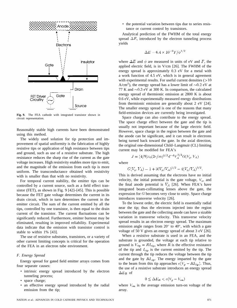
Fig. 9. The FEA cathode with integrated transistor shown incircuit representation.
Reasonably stable high currents have been demonstratedusing this method.
The widely used solution for tip protection and im-provement of spatial uniformity is the fabrication of highlyresistive tips or application of high resistance between tipsand ground, such as use of a resistive substrate. The highresistance reduces the sharp rise of the current as the gatevoltage increases. High resistivity enables more tips to emit,and the magnitude of the emission from each tip is moreuniform. The transconductance obtained with resistivitywith is smaller than that with no resistivity.
For temporal current stability, the emitter tips can becontrolled by a current source, such as a field effect tran-sistor (FET), as shown in Fig. 9 [42]–[45]. This is possiblebecause the FET gate voltage determines the current in itsdrain circuit, which in turn determines the current in theemitter circuit. The sum of the current emitted by all thetips, controlled by one transistor, is then equal to the draincurrent of the transistor. The current fluctuations can besignificantly reduced. Furthermore, emitter burnout may beeliminated, resulting in improved reliability. Experimentaldata indicate that the emission with transistor control isstable to within 1% [43].
The use of resistive substrates, transistors, or a variety ofother current limiting concepts is critical for the operationof the FEA in an electron tube environment.
F. Energy Spread
Energy spread for gated field emitter arrays comes fromfour separate causes:
• intrinsic energy spread introduced by the electrontunneling process;
• space charge;• an effective energy spread introduced by the radial
emission from the tip;
• the potential variation between tips due to series resis-tance or current control by transistors.
Analytical prediction of the FWHM of the total energyspread , introduced by the electron tunneling processyields
where and are measured in units of eV and, theapplied electric field, is in V/cm [26]. The FWHM of theenergy spread is approximately 0.3 eV for a metal witha work function of 4.5 eV, which is in general agreementwith experimental results. For useful current densities (A/cm ), the energy spread has a lower limit of eV at77 K and eV at 300 K. In comparison, the calculatedenergy spread of thermionic emission at 2800 K is about0.6 eV, while experimentally measured energy distributionsfrom thermionic emission are generally about 2 eV [24].The smaller energy spread is one of the reasons that manyfield-emission devices are currently being investigated.
Space charge can also contribute to the energy spread.The space charge effect between the gate and the tip isusually not important because of the large electric field.However, space charge in the region between the gate andthe anode can be significant, and it can result in electronsbeing turned back toward the gate. In the axial direction,the original one-dimensional Child–Langmuir (CL) limitingcurrent may be modified for FEA’s
where
This is derived assuming that the electrons have no initialvelocity, the initial potential is the gate voltage, , andthe final anode potential is [26]. When FEA’s haveintegrated beam-collimating lenses above the gate, theexpression for becomes very close to unity. Space chargeintroduces transverse velocity [26].
To the lowest order, the electric field is essentially radialnear the tip; thus the electrons injected into the regionbetween the gate and the collecting anode can have a sizablevariation in transverse velocity. This transverse velocityspread results in an electron energy spread. The maximumemission angle ranges from 20to 40 , with which a gatevoltage of 50 V gives an energy spread of about 3 eV [26].
When a resistive substrate is used in an FEA, and thesubstrate is grounded, the voltage at each tip relative toground is , where is the effective resistanceof the tip and is the current emitted by the tip. Thecurrent through the tip reduces the voltage between the tipand the gate by . The energy imparted by the gateto the beam from this tip approaches . Thus,the use of a resistive substrate introduces an energy spread
of
where is the average emission turn-on voltage of thearray.
NATION et al.: ADVANCES IN COLD CATHODE PHYSICS AND TECHNOLOGY 871
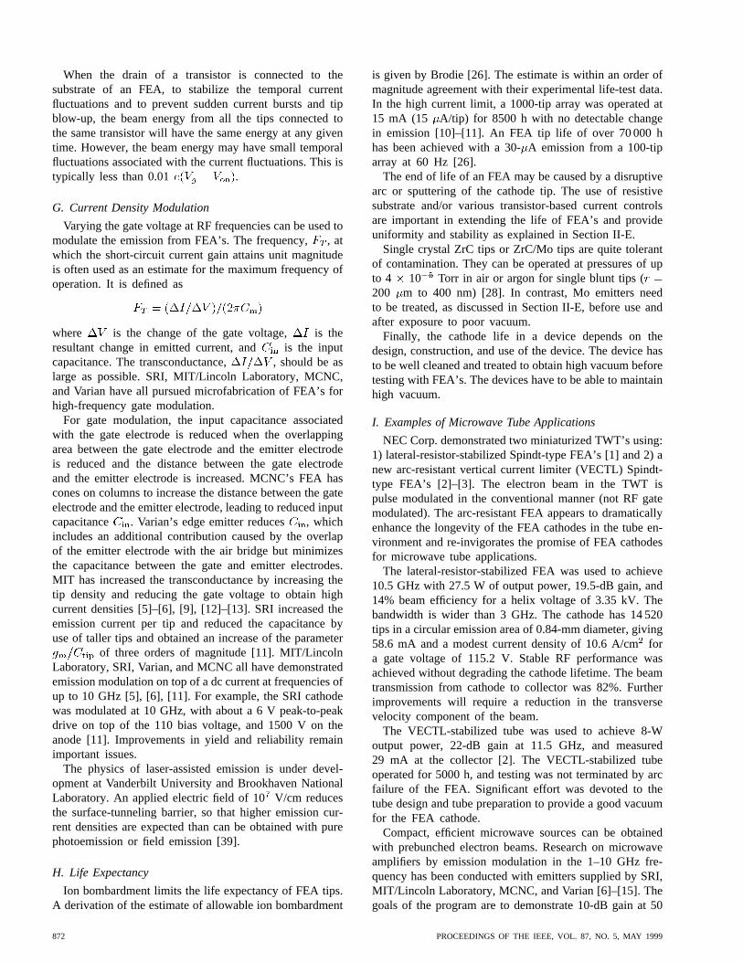
When the drain of a transistor is connected to thesubstrate of an FEA, to stabilize the temporal currentfluctuations and to prevent sudden current bursts and tipblow-up, the beam energy from all the tips connected tothe same transistor will have the same energy at any giventime. However, the beam energy may have small temporalfluctuations associated with the current fluctuations. This istypically less than 0.01 .
G. Current Density Modulation
Varying the gate voltage at RF frequencies can be used tomodulate the emission from FEA’s. The frequency,, atwhich the short-circuit current gain attains unit magnitudeis often used as an estimate for the maximum frequency ofoperation. It is defined as
where is the change of the gate voltage, is theresultant change in emitted current, and is the inputcapacitance. The transconductance, , should be aslarge as possible. SRI, MIT/Lincoln Laboratory, MCNC,and Varian have all pursued microfabrication of FEA’s forhigh-frequency gate modulation.
For gate modulation, the input capacitance associatedwith the gate electrode is reduced when the overlappingarea between the gate electrode and the emitter electrodeis reduced and the distance between the gate electrodeand the emitter electrode is increased. MCNC’s FEA hascones on columns to increase the distance between the gateelectrode and the emitter electrode, leading to reduced inputcapacitance . Varian’s edge emitter reduces , whichincludes an additional contribution caused by the overlapof the emitter electrode with the air bridge but minimizesthe capacitance between the gate and emitter electrodes.MIT has increased the transconductance by increasing thetip density and reducing the gate voltage to obtain highcurrent densities [5]–[6], [9], [12]–[13]. SRI increased theemission current per tip and reduced the capacitance byuse of taller tips and obtained an increase of the parameter
of three orders of magnitude [11]. MIT/LincolnLaboratory, SRI, Varian, and MCNC all have demonstratedemission modulation on top of a dc current at frequencies ofup to 10 GHz [5], [6], [11]. For example, the SRI cathodewas modulated at 10 GHz, with about a 6 V peak-to-peakdrive on top of the 110 bias voltage, and 1500 V on theanode [11]. Improvements in yield and reliability remainimportant issues.
The physics of laser-assisted emission is under devel-opment at Vanderbilt University and Brookhaven NationalLaboratory. An applied electric field of 10V/cm reducesthe surface-tunneling barrier, so that higher emission cur-rent densities are expected than can be obtained with purephotoemission or field emission [39].
H. Life Expectancy
Ion bombardment limits the life expectancy of FEA tips.A derivation of the estimate of allowable ion bombardment
is given by Brodie [26]. The estimate is within an order ofmagnitude agreement with their experimental life-test data.In the high current limit, a 1000-tip array was operated at15 mA (15 A/tip) for 8500 h with no detectable changein emission [10]–[11]. An FEA tip life of over 70 000 hhas been achieved with a 30-A emission from a 100-tiparray at 60 Hz [26].
The end of life of an FEA may be caused by a disruptivearc or sputtering of the cathode tip. The use of resistivesubstrate and/or various transistor-based current controlsare important in extending the life of FEA’s and provideuniformity and stability as explained in Section II-E.
Single crystal ZrC tips or ZrC/Mo tips are quite tolerantof contamination. They can be operated at pressures of upto 4 10 Torr in air or argon for single blunt tips (200 m to 400 nm) [28]. In contrast, Mo emitters needto be treated, as discussed in Section II-E, before use andafter exposure to poor vacuum.
Finally, the cathode life in a device depends on thedesign, construction, and use of the device. The device hasto be well cleaned and treated to obtain high vacuum beforetesting with FEA’s. The devices have to be able to maintainhigh vacuum.
I. Examples of Microwave Tube Applications
NEC Corp. demonstrated two miniaturized TWT’s using:1) lateral-resistor-stabilized Spindt-type FEA’s [1] and 2) anew arc-resistant vertical current limiter (VECTL) Spindt-type FEA’s [2]–[3]. The electron beam in the TWT ispulse modulated in the conventional manner (not RF gatemodulated). The arc-resistant FEA appears to dramaticallyenhance the longevity of the FEA cathodes in the tube en-vironment and re-invigorates the promise of FEA cathodesfor microwave tube applications.
The lateral-resistor-stabilized FEA was used to achieve10.5 GHz with 27.5 W of output power, 19.5-dB gain, and14% beam efficiency for a helix voltage of 3.35 kV. Thebandwidth is wider than 3 GHz. The cathode has 14 520tips in a circular emission area of 0.84-mm diameter, giving58.6 mA and a modest current density of 10.6 A/cmfora gate voltage of 115.2 V. Stable RF performance wasachieved without degrading the cathode lifetime. The beamtransmission from cathode to collector was 82%. Furtherimprovements will require a reduction in the transversevelocity component of the beam.
The VECTL-stabilized tube was used to achieve 8-Woutput power, 22-dB gain at 11.5 GHz, and measured29 mA at the collector [2]. The VECTL-stabilized tubeoperated for 5000 h, and testing was not terminated by arcfailure of the FEA. Significant effort was devoted to thetube design and tube preparation to provide a good vacuumfor the FEA cathode.
Compact, efficient microwave sources can be obtainedwith prebunched electron beams. Research on microwaveamplifiers by emission modulation in the 1–10 GHz fre-quency has been conducted with emitters supplied by SRI,MIT/Lincoln Laboratory, MCNC, and Varian [6]–[15]. Thegoals of the program are to demonstrate 10-dB gain at 50
872 PROCEEDINGS OF THE IEEE, VOL. 87, NO. 5, MAY 1999
W and 10 GHz with 50% efficiency in a gated klystrodeamplifier tube, headed by CPI, and a twystrode tube headedby Naval Research Laboratory.
J. Summary
Field-emission tips and arrays have made significantadvances in recent years as high current density coldcathodes. Many applications of field emitter arrays arebeginning to be realized, such as scanning tunneling andatomic force microscopes, and flat panel field-emissiondisplays.
The applications of FEA’s for power tubes and accelera-tors are more demanding because they require many ordersof magnitude higher total current and current density andtypically operate at higher voltages. Temporal stability andemission uniformity of the FEA’s have been significantlyimproved with resistive substrates and active and passivecurrent control. The ZrC or ZrC/Mo tips are promisingbecause of their low work functions and resistance tocontamination and back ion bombardment. For low currentapplications, which require no more than a few tens ofmA of current, single ZrC or ZrC/Mo tips will providethe brightest sources. Areas that still require improvementfor FEA’s are integrated beam collimating lenses, highertotal current, large current density modulation at gigahertzfrequencies, all, of course, with long lifetime.
Design and construction of tubes and accelerators withfield-emission cathodes must take into account the op-erational characteristics of FEA’s. This process wouldnot only make it more likely to realize the designeddevice characteristics, but it would also improve FEAlifetimes. Field-emission cathodes have the potential tomake improvements in a variety of electron devices andto enable new applications [46]–[47].
III. A DVANCES IN ELECTRON SOURCE
DEVELOPMENT: PHOTOEMISSION
A. Introduction
In the past decade, there has been renewed interest in pho-tocathodes as a source for high brightness electron beams.When the photocathodes are irradiated by laser to generateelectron bunches, unprecedented control over the electronpeak current, and spatial profile and temporal profile couldbe achieved by controlling the laser pulse incident on thephotocathode. With the advent of high power, short pulselasers [48], [49], it is now possible to generate electronswith bunch lengths less than 30-m and charges exceedingtens of nanocoulombs. Waveform shaping devices [50]–[54]can be used in the laser propagation system to generateelectron bunches with a wide variety of temporal and spatialprofiles. Laser pulse trains can be generated either directlyfrom the lasers [55] or by optical multiplexing [56].
Until recently, photocathodes have been used mainly assources of prebunched electron beams in RF linacs. In thisapplication, a laser beam irradiating a photocathode in ashort accelerating RF structure generates the modulated
Fig. 10. Schematic of an RF injector: (A) photocathode, an inte-gral part of the RF accelerating structure; (B) accelerating structure;(C) laser to drive the photocathode; (D) master clock triggeringboth the laser and the RF structure to achieve synchronism.
Fig. 11. Schematic of two-beam accelerator.
electron beam. The accelerating gradient in the structure isin the range of 50–100 MV/m. So the electron bunches arerapidly brought to a few MeV and the debunching effectsof the space charge are minimized prior to subsequent ac-celeration in the linac. A schematic of such a photoinjectoris shown in Fig. 10.
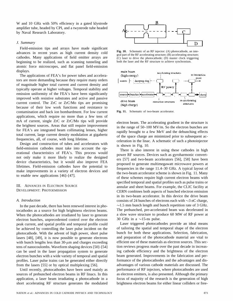
There is also interest in using these cathodes in highpower RF sources. Devices such as gyroharmonic convert-ers [57] and two-beam accelerators [56], [58] have beenproposed to generate multimegawatt microwave powers atfrequencies in the range 11.4–30 GHz. A typical layout ofthe two-beam accelerator scheme is shown in Fig. 11. Manyof these schemes require high current electron beams withspecified temporal and spatial profiles such as pulse trains orannular and sheet beams. For example, the CLIC facility atCERN combines both aspects of bunched electron emissionin its two-beam accelerator. In this device the drive beamconsists of 24 bunches of electrons each with3 nC charge,
1.5 mm bunch length and bunch repetition rate of 3 GHz.The prebunched, pre-accelerated beam was decelerated ina slow wave structure to produce 60 MW of RF power at30 GHz in a 15-ns pulse.
Laser triggered photocathodes provide an ideal meansof tailoring the spatial and temporal shape of the electronbunch for both these applications. Selection, fabrication,and preparation of the photocathode material are vital toefficient use of these materials as electron sources. This sec-tion reviews progress made over the past decade in increas-ing cathode efficiency and the brightness of the electronbeam generated. Improvements in the fabrication and per-formance of the photocathodes and the advantages and dis-advantages of various cathode materials are discussed. Theperformance of RF injectors, where photocathodes are usedas electron emitters, is also presented. Although the primaryfocus of majority of the research is the generation of highbrightness electron beams for either linear colliders or free-
NATION et al.: ADVANCES IN COLD CATHODE PHYSICS AND TECHNOLOGY 873
electron lasers (FEL’s), the results are also relevant for RFpower generation. The review is limited to simple metal andsemiconductor cathodes as they are the most promising.
B. Fabrication and Performance of Photocathodes
Critical to the design of the photoinjector is the choice ofthe photocathode and the laser system. These two factorsdetermine the reliability and complexity of the system.Normally, the photocathode material is either a simplemetal or a cesiated metal/semiconductor. Simple metalphotocathodes are rugged, relatively insensitive to contami-nation, can be operated in moderate vacuum levels of 10Torr, and have lifetimes of the order of years. However,the high work function typical of metals requires the use ofUV lasers and even then, the quantum efficiency is only inthe order of 10 . Cesiated cathodes, on the other hand,have 10% quantum efficiency but suffer from shorterlifetime of a few hours and poisoning due to contamination.There has been extensive research in the past decade toimprove the performance of both types of cathodes. In thesubsequent section, the relative merits of these cathodes aswell as fabrication techniques are described.
1) Metal Photocathodes:Metal photocathodes have beenstudied extensively over a long period due to their simplic-ity of preparation and availability [59]. In addition, interestin these cathodes has revived in recent years as a possiblesource of high-brightness electron beams. The primary ad-vantage of these types of cathode is their fast response time,ease of preparation, relative insensitivity to contamination,and the long lifetime. However, the high work function,typical of metal cathodes, necessitates UV irradiation ofthe cathodes to obtain reasonable electron yield. Recentresearch efforts have focused on reducing the work functionand improving the system efficiency. The quantum effi-ciency (QE) of a vast array of metal cathodes has beentested under dc bias [60], [61]. Different techniques toimprove the QE have been investigated on more promis-ing candidates. In most measurements, the QE was verysensitive to the sample preparation technique, varying overa factor of two for different techniques. The best resultswere obtained [62] when the samples were polished with 1-
m diamond polishing compound (Buehler Metadi diamondsuspension for polishing with Buehler Metadi fluid extenderfor diamond abrasives as lubricant) to remove the surfacelayer. This must be followed by cleaning with hexane inultrasonic cleaner to remove any residue prior to testing.
The QE of metal cathodes has been improved by avariety of techniques, including irradiating the sample withhigh-power UV laser in vacuum [63] to remove surfacecontamination, irradiating the cathode near the Brewster’sangle, orienting the electric field of the laser in the plane ofincidence [64], and operating the cathode in high electricfields [65], [66] to reduce the work function due to theSchottky effect. So far the highest QE obtained with a 266-nm laser beam has been 410 using Mg cathode [67].The most promising metal cathodes so far are copper (Cu)[68]–[70] and magnesium (Mg). Both of them have highquantum efficiencies (0.4% for Mg and 0.05% for Cu) and
high optical damage thresholds (0.1 mJ/mmfor Mg and 1mJ/mm for Cu). They can also be transported in air, arerelatively insensitive to contaminants, and have lifetimesof years. (In the majority of cases, the lifetime tests wereterminated for reasons other than the degradation of thecathode material.)
Charges exceeding tens of nanocoulombs in 10-ps pulseshave been obtained with both Cu and Mg cathodes. Trainsof 72 pulses, each with 0.5-nC charge, have been generatedwith Mg photocathodes. Most of the metals tested did notshow a significant change in the quantum efficiency if thevacuum conditions and the contaminants in the vacuum didnot change and the samples were prepared carefully. Whencathodes in RF guns were exposed to RF breakdowns, thequantum efficiency was seen to decrease by factors of four.However, this drop was remedied by subsequent scanningwith a high-power laser.
Metal-like LaB cathode has been tested in the presenceof both dc and rf fields. With a dc bias, a QE of6 10has been obtained with 266 nm after heating the cathodebriefly to 1550C [71]. In the presence of rf fields, thesample had to be kept at 800C to preserve the QE [72].Current limitation of LaB has not yet been studied.
2) Semiconductor Cathodes:Another promising familyof photoemitters is the alkali-based semiconductor cath-odes. Tri-alkali and bi-alkali cathodes such as NaKSb:Csand K CsSb have been used in photomultipliers asefficient electron emitters [73]. However, their sensitivityto contamination had been the main deterrent for usingthem in other electron emission applications. Relativelyinsensitive cathodes such as CsI require photon energiesin excess of 6 eV for high electron yield. In recent years,significant advances have been made both in the fabricationand in prolonging the lifetime of these cathodes. Table 2provides a more extensive comparison of performancefrom different cathode materials.
In Section III-C, we present results from the morepromising CsTe cathodes. They are typically fabricatedusing an ultrahigh vacuum chamber where 10–30 nm ofTe are deposited on a substrate (Cu, Mo, and Mg) atroom temperature. Cs is evaporated onto the film with thesubstrate heated to 110C until the photoemission reachesits maximum. Freshly prepared cathodes, grown on Cu andMo substrates, were shown to yield a QE in the range of6%–12% at 266 nm [74], [75] and 16% at 251 nm [76].This QE was shown [74] to be sensitive to the presenceof O and relatively insensitive to contamination of CO,N , and CH . The QE of an oxygen exposed surface couldbe restored to 30% of its original value by simultaneouslyheating the sample to 230C and irradiating it with 254-nmlight from a mercury lamp. During the operation of thephotocathode in a RF cavity the QE decreased roughlyas a sequence of two exponential decays, a fast decreasewith a decay time of tens of hours, lasting for 1–2 days,followed by a slow decay with a decay time of hundredsof hours. Electron bunches with up to 35-nC charge and afew picoseconds pulse duration have been generated withthese cathodes.
874 PROCEEDINGS OF THE IEEE, VOL. 87, NO. 5, MAY 1999
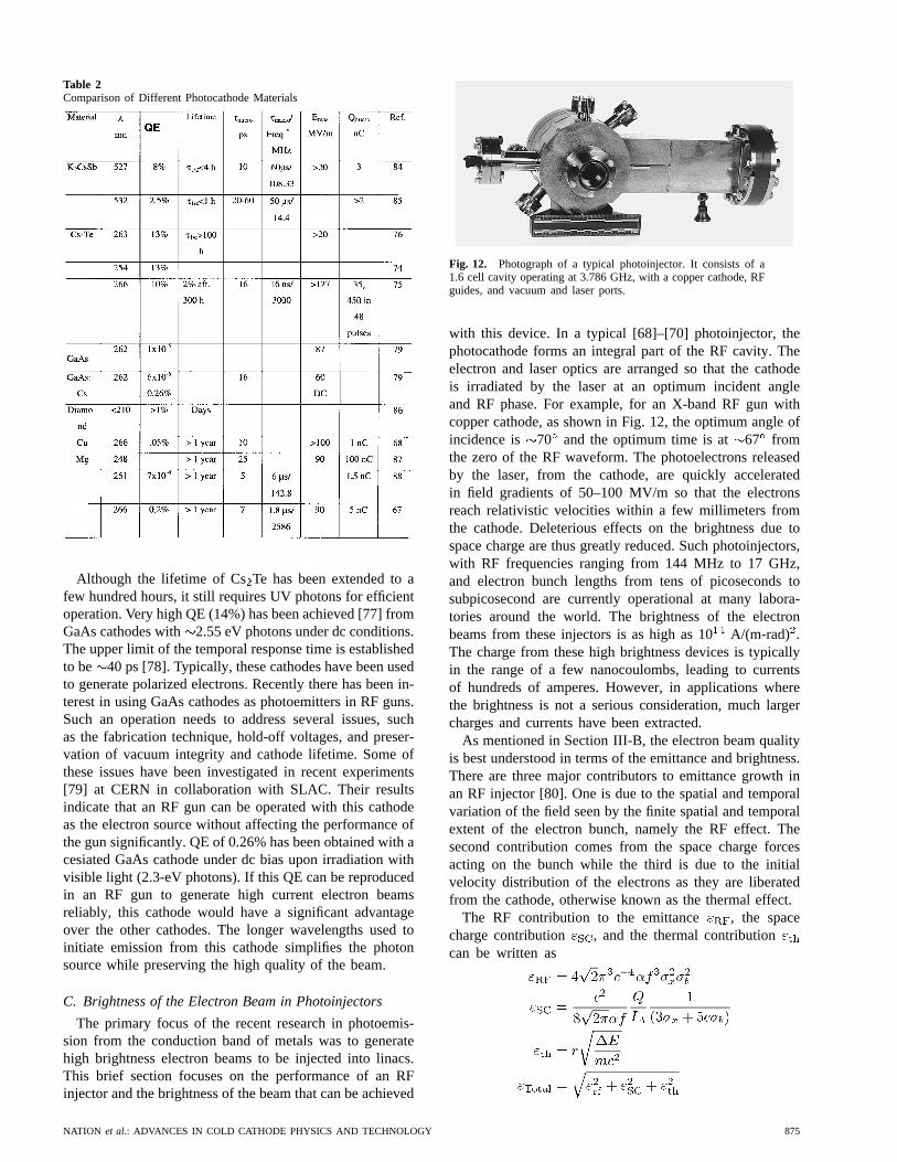
Table 2Comparison of Different Photocathode Materials
Although the lifetime of CsTe has been extended to afew hundred hours, it still requires UV photons for efficientoperation. Very high QE (14%) has been achieved [77] fromGaAs cathodes with 2.55 eV photons under dc conditions.The upper limit of the temporal response time is establishedto be 40 ps [78]. Typically, these cathodes have been usedto generate polarized electrons. Recently there has been in-terest in using GaAs cathodes as photoemitters in RF guns.Such an operation needs to address several issues, suchas the fabrication technique, hold-off voltages, and preser-vation of vacuum integrity and cathode lifetime. Some ofthese issues have been investigated in recent experiments[79] at CERN in collaboration with SLAC. Their resultsindicate that an RF gun can be operated with this cathodeas the electron source without affecting the performance ofthe gun significantly. QE of 0.26% has been obtained with acesiated GaAs cathode under dc bias upon irradiation withvisible light (2.3-eV photons). If this QE can be reproducedin an RF gun to generate high current electron beamsreliably, this cathode would have a significant advantageover the other cathodes. The longer wavelengths used toinitiate emission from this cathode simplifies the photonsource while preserving the high quality of the beam.
C. Brightness of the Electron Beam in Photoinjectors
The primary focus of the recent research in photoemis-sion from the conduction band of metals was to generatehigh brightness electron beams to be injected into linacs.This brief section focuses on the performance of an RFinjector and the brightness of the beam that can be achieved
Fig. 12. Photograph of a typical photoinjector. It consists of a1.6 cell cavity operating at 3.786 GHz, with a copper cathode, RFguides, and vacuum and laser ports.
with this device. In a typical [68]–[70] photoinjector, thephotocathode forms an integral part of the RF cavity. Theelectron and laser optics are arranged so that the cathodeis irradiated by the laser at an optimum incident angleand RF phase. For example, for an X-band RF gun withcopper cathode, as shown in Fig. 12, the optimum angle ofincidence is 70 and the optimum time is at 67 fromthe zero of the RF waveform. The photoelectrons releasedby the laser, from the cathode, are quickly acceleratedin field gradients of 50–100 MV/m so that the electronsreach relativistic velocities within a few millimeters fromthe cathode. Deleterious effects on the brightness due tospace charge are thus greatly reduced. Such photoinjectors,with RF frequencies ranging from 144 MHz to 17 GHz,and electron bunch lengths from tens of picoseconds tosubpicosecond are currently operational at many labora-tories around the world. The brightness of the electronbeams from these injectors is as high as 10A/(m-rad) .The charge from these high brightness devices is typicallyin the range of a few nanocoulombs, leading to currentsof hundreds of amperes. However, in applications wherethe brightness is not a serious consideration, much largercharges and currents have been extracted.
As mentioned in Section III-B, the electron beam qualityis best understood in terms of the emittance and brightness.There are three major contributors to emittance growth inan RF injector [80]. One is due to the spatial and temporalvariation of the field seen by the finite spatial and temporalextent of the electron bunch, namely the RF effect. Thesecond contribution comes from the space charge forcesacting on the bunch while the third is due to the initialvelocity distribution of the electrons as they are liberatedfrom the cathode, otherwise known as the thermal effect.
The RF contribution to the emittance , the spacecharge contribution , and the thermal contributioncan be written as
NATION et al.: ADVANCES IN COLD CATHODE PHYSICS AND TECHNOLOGY 875
where is the velocity of light, is a dimensionlessfactor representing the strength of the accelerating fieldand is the RF wave number, is theRF frequency, is the rms transverse beam size,is therms bunch length in time, is the charge, is the Alfvencurrent 17 000 A, and is the difference between thephoton energy and the cathode work function.
As can be seen from these equations, operating the injec-tors at higher accelerating gradient [70] could reduce theemittance growth from space charge forces. Alternatively,emittance growth can be compensated using solenoidalmagnets specifically designed for the injector and the beamcurrent [68]. Normalized transverse emittances of0.7mm-mrad have been achieved with 0.3-nC beams using thelatter method [81]. The slice emittance of this beam hasbeen shown to be much better indicating that the emittancecould be improved even further. The energy spread of theelectron bunch in these devices is typically less than 1%.
D. Photocathodes in Power Generation
In this section, results of a proof-of-principle experimentto generate RF power at 30 GHz using a train of pulseswill be discussed. In the two-beam accelerator scheme,originally proposed by Sessler in 1982 [82], a high currentdrive beam supplies energy to the main linac at regularintervals via transfer structures. FEL’s and deceleratingcavities [83] have been proposed as transfer structures.The latter transfer structure has been tested along with thegeneration of a high current drive beam in the CLIC TestFacility at CERN [75]. The drive beam was generated in a3-GHz, 1.5 cell RF gun operating at 100 MV/m field andequipped with a laser driven CsTe photocathode. CsTecathodes were irradiated by10-ps long fourth harmonicradiation at 262 nm from a Nd:YAG laser. The gun couldbe operated either in a single or a multiple bunch mode.The multiple bunches were made by splitting a singlelaser pulse into a train of pulses, each spaced by one 3-GHz wavelength. The energy of the bunched electron beamexiting the gun is increased to 11 MeV in a booster cavityand to 95 MeV in a long traveling wave section. The energywas extracted from the beam at 30 GHz by a 30-cm longtraveling wave section.
In the first set of experiments, 76 MW of RF powerwas generated by a train of 48 bunches of electrons, with3 nC charge per bunch. This power level corresponds toa decelerating field of 124 MV/m. The electron bunchlength measured after the gun booster cavity was 8–17 ps(FWHM). With an upgraded system, 60 MW of RF powerhas been generated routinely by a train of 24 bunches with amomentum of 63 MeV/c. In the upgrade, a magnetic bunchcompressor was added to reduce the electron bunch length.The measurement of the bunch length after the compressorwas limited by the 5-ps resolution of the instrument. Thistest facility has clearly demonstrated the principle of thetwo-beam accelerator scheme and also serves to illustratethe utility of photo-emitters as beam bunching devices inhigh-power RF sources.
The second phase of the facility is now under con-struction. The primary goal of this phase is to study thefeasibility of the scheme with parameters close to the CLIC.One component of the investigation is the production of480 MW of RF power at 30 GHz for beam acceleration upto 320 MeV. In this phase, the charge per bunch will beincreased to 13.4 nC, with 48 bunches per train at 3 GHzbunch repetition frequency, leading to a total charge of 0.64
C in 16 ns. A probe beam with 1.3 nC will be acceleratedwith the power derived from the drive beam.
These studies illustrate the use of photocathodes aselectron sources in generating high RF power at highfrequencies. The capability of the photocathodes to generatevery large charge in a very short (10 ps) time is crucialfor the success of these programs.
Extensive research in the past decade has led to signif-icant improvement in the performance of photocathodes.Fabrication techniques of the cathodes have been refinedto yield reproducible cathodes. Lifetimes of semiconductorcathodes have been extended from a few hours to a fewhundred hours. Similarly, the quantum efficiencies of metalcathodes have increased from 10to 10 . Both types ofcathodes have been used to generate tens of nanocoulombsin a single pulse of a few picoseconds duration as wellas to generate pulse trains. With the advent of GaAs:Cscathodes in RF cavities, it may be possible to generatesimilar electron bunches with visible photons instead ofUV photons in the foreseeable future, making the lasertriggered photoemitter an easily controllable, inexpensive,reliable source of electrons. Their capability to generatecharges exceeding 50 nC in pulse durations of10 psidentify them as potentially very good electron sourcesfor RF power generation at high frequencies. The highbrightness achievable with these cathodes also makes themideal source for linacs.
IV. ELECTRON EMISSION FROM
FERROELECTRICCERAMICS
A. Introduction
Among the various electron-emission mechanisms re-viewed in this article, emission from ferroelectric ceramicsis the “junior” process. It was observed as a curiosityin 1984 by Rosenman [89] who found current densitiesof the order of 10 pA/cm. Five years later Riege andhis co-workers at CERN reported currents which were 13orders of magnitude higher [90]. In 1990 Airapetov [91]reported the highest current density so far (400 A/cm).Beam-emitting areas of order 1 cmare common so largecurrents of 1 kA are obtained in present-day experiments.Work in the United States was started at Cornell University[92]–[93] in 1990 and this effort has expanded to includegroups at Integrated Applied Physics (IAP) in collaborationwith MIT [94], Lawrence Livermore National Labora-tory (LLNL) [95], and the University of New Mexico[96]. In parallel the topic has been investigated in Japan[97].
876 PROCEEDINGS OF THE IEEE, VOL. 87, NO. 5, MAY 1999
Electron emission from ferroelectrics may be broadlydivided into two categories. The first of these occurs whenan applied electric field induces a phase transition from theanti-ferroelectric to the ferroelectric state and, the secondin emission occurring as a result of rapid changes in theferroelectric state of the material, i.e., it is switched arounda minor hysteresis loop. The work of Riegeet al. and that ofthe University of New Mexico group deals with the formersituation, whereas most of the remaining work is associatedwith material which is always in the ferroelectric state.Many of the electron-emission features are common to bothregimes including, the large value of the dielectric constant,the nonlinear dependence on the applied electric field,the requirement of a threshold field to trigger emission,and the role of surface charges in screening the effect ofthe material polarization from the region external to theferroelectric. The ceramic-vacuum boundary electric field,which is developed as a result of the field applied to theceramic, is extremely large due to the high value of thedielectric constant of the ceramic. This implies that therole of field emission in determining the electron currentcannot be ignored. Field emission may also lead to plasmaformation at microprotusions on the cathode surface andwith sufficient time result in gap closure.
If electron emission occurs as a result of a phase tran-sition, the characteristics of the emission are dramaticallydifferent to those found when the ferroelectric is switchedaround a hysteresis loop.
On the other hand, the initial polarization of the ceramiconly has a weak effect on the emission. In all the cases tobe discussed, the dielectric properties are nonlinear and theeffective dielectric constant is larger than unity by at leasttwo orders of magnitude.
We make these comments before we describe the char-acteristics and modeling of electron emission from a fer-roelectric because the character of the emission dependson these characteristics and, as will be discussed later,the interpretations of the phenomena are not universallyaccepted. We now summarize experimental observationsmade of electron emission from ferroelectrics and thenoutline interpretations of the emission mechanisms.
B. Overview of Experimental Results
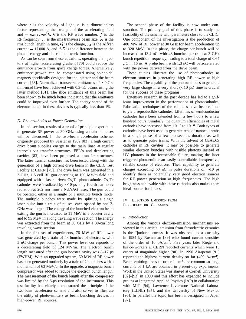
We consider a typical experimental arrangement as shownin Fig. 13. The cathode consists of a ferroelectric “capac-itor” with a uniformly silvered back electrode. The frontelectrode has a thin metallic grid covering the surface.Most of the data obtained to date uses a planar diode tostudy the emission; some work has however been reportedin gun assemblies. When a rapidly changing electric fieldof order 10 kV/cm is applied to the ceramic, a currentflows in the diode gap. The current density is many ordersof magnitude higher than that measured in the absence ofthe triggering field. The effects of the ceramic polarization
10–40 C/cm are screened from the external world bycharges drawn from the surroundings to the surface of theferroelectric.
Fig. 13. Typical assembly used for the study of emission from aferroelectric cathode.
The anode current mentioned above is only weaklydependent on the initial polarization of the ceramic. Inthe case where emission arises due to a phase transition,a burst of energetic electrons with energies up to 25 keV[90] has been measured. This is accompanied by a burst ofmicrowave radiation in the gigahertz range [91]. In all othercases, energetic electron emission is also observed but theelectron energies found are typically lower, of order of orless than 1 keV.
We now summarize some of the experimental results.
• The anode current pulse is, for a wide range ofanode–cathode (A–K) gaps (0.1–5 cm), determined bythe anode voltage pulse and not by that of the ferro-electric voltage. The initial current flow is controlledby the ferroelectric. At later times, plasma closes theA–K gap and the current flow is then controlled byplasma processes [89].
• Current densities of more than 100 A/cmwere mea-sured at CERN [90] in vacuum diodes even in theabsence of an externally applied extraction field, butonly with small A–K gaps. At Cornell similar currentdensities 120 A/cm were measured for anode volt-ages of up to 50 kV and with gaps of order 5 cm [89].Experiments by Airapetov [91] have shown currentdensities of 400 A/cm accompanied by substantialcathode erosion.
• The I–V characteristic of the diode is linear within areasonable approximation. This result is valid for lowvoltages [92] ( 1 kV) and for short diode gaps (1.5cm) as well as for high anode voltage 50 kV withgaps of up to 5 cm [89]. All groups’ report that for thetypical geometries the current exceeds that predictedby the Child–Langmuir (CL) relationship.
• The energy of the emitted electrons as determined byback biasing of the anode is found to depend on thepolarity of the voltage applied on the back of theferroelectric [89]. In the case of a positive voltage,the energy is of the order of 100 eV and in the caseof negative pulse the energy is1 keV. Substantiallyhigher energies (25 keV) have been measured by Riege[92] and have been inferred by the LLNL group [95]based on a theoretical model.
NATION et al.: ADVANCES IN COLD CATHODE PHYSICS AND TECHNOLOGY 877
• The Q-V characteristic of the ferroelectric capacitor ishighly nonlinear during the switching pulse durationand follows a hysteresis-like curve [92], [93], [96].The off-equilibrium state of the ferroelectric lasts forat least 1 s.
• At LLNL [95] it was observed that the anode currentincreases with a delay between the voltage pulses ap-plied to the ferroelectric and the anode; the maximumoccurred with a delay of 450 ns and with longer delaysthe current decreases. A similar behavior was observedat Cornell with the maximum current occurring witha 1- s delay [97]. Beyond this time the current dropsand vanishes with a delay greater than 2.5s.
• Several groups have measured the electron beam emit-tance and brightness: IAP [94] for a 36-A, 22.5-kVbeam reported a brightness of 10A/m rad . AtLLNL [95] the lower estimate of the brightness was10 A/m rad for currents of 6 A at 11 kV and 42A at 21 kV. At Cornell, the brightness was measured[100] at 14 kV and 8 A. Its value was found to be 1.2
10 A/m rad .• Riege and his collaborators [98], [101], [102] have
found that illuminating the surface facilitates emissionof electrons by laser light. The basic expectation wasthat screening electrons would be released by thephotons. When electrons of more than 10 keV weremeasured, it became evident that the photons affectthe polarization of the material. It seems likely thatthe material undergoes a phase-transition locally andthis generates the energetic electron flux.
• Several authors measured good repetitive pulses: Riegehas reported [98] reproducible 5-ns pulses over morethan 10 shots. At Cornell, reproducible pulses at 15kV, 20 A, and 600 ns were measured at50 Hz. TheLLNL group observed no degradation of the currentpulse at 1 Hz for more than 20 000 shots with anodevoltages between 15 to 60 kV.
• There is a small delay (50 ns) between the applica-tion of the voltage on the ferroelectric and the start ofthe current [102].
• From the experience of the Cornell group it seems thatthere is no substantial dependence of the performanceof the cathode on the initial polarity of the ferro-electric sample; the timing of the emission pulses aresomewhat different but the current levels are similar.
• Some electron gun experiments have been carried outat beam energies of up to 500 keV, and beam currentsof up to 350 A from a 1.9-cm diameter ferroelectricdisk. Preliminary data show no evidence of erosionof the cathode surface in the gun geometry. Resultsusing similar geometries, but at 15 keV, have shownlittle erosion over extended periods of operation. Thisis in contrast to the situation found in a planar diodewhere back bombardment of the cathode surface limitsrepeatability and the cathode life.
The experimental results indicate that a cathode made offerroelectric ceramic has the potential to generate a highbrightness and repetitive electron beam for a variety of
applications. Ferroelectric emitters possess several uniqueproperties. In Section IV-C, we shall discuss the variousmodels which have been developed in recent years toexplain the observations.
C. Overview of Theoretical Models
A comprehensive theory that can explain all the experi-mental results listed in Section IV-B does not exist today.However, several models have been developed throughoutthe years that shed light on the physical processes that occurduring emission.
1) Riege’s Model:Riege [98] has summarized a qualita-tive explanation for the presence of the energetic electronsfound in most experiments. An internal polarization field ina ferroelectric is screened from the external world by a layerof free charge on the surface of the ceramic. In comparisonwith the situation in ferromagnets, where magnetic fieldsare measured outside the material, no electric field existsoutside the ferroelectric sample. If the polarization fieldin the material is altered by some external means, say byapplying a short voltage pulse, then part of the free chargeattached to the surface by the original polarization field mayleave the system. If an applied field reverses the polarizationfield, then the surface neutralizing charge is repelled andacquires a kinetic energy associated with the energy storedin the reversed polarization field.
2) Redistribution Cloud Model:This model has been de-veloped at Cornell based on experimental data accumulatedthere during two years of experiment [93]. It is the onlydetailed quantitative theory of ferroelectric emission thathas been developed to date. Its basic assumption is thatelectrostatic coupling to the fields in the ferroelectric con-trols the dynamics of electrons in the diode gap. It istherefore essential to be able to understand the nonlineardynamics (hysteresis) of the ceramic. For this purpose,the Weiss model for ferromagnetic materials was adaptedto ferroelectric ceramics to provide the following relationbetween the normalized polarization field andthe normalized electric field
where is the microscopic dipole moment,is the maximum value of the polarization field,
is the characteristic dielectric coefficientof the material, , and is the characteristicresponse time of the material. This equation exhibits therequired ferroelectric hysteresis between and andalso allows for prepoling of the ceramic. With the po-larization field known, one can determine the charge onthe surface at any point in time. In particular, one canestablish the change in the charge arising from departuresfrom the equilibrium state. For simplicity, we shall assumethat there is an excess of electrons on the gridded electrodefacing the A–K gap. When the ferroelectric is pulsed wefurther assume that a substantial fraction of the excess ofsurface charge redistributes within the A–K gap, with therest flowing to the surrounding grid. In order to understand
878 PROCEEDINGS OF THE IEEE, VOL. 87, NO. 5, MAY 1999
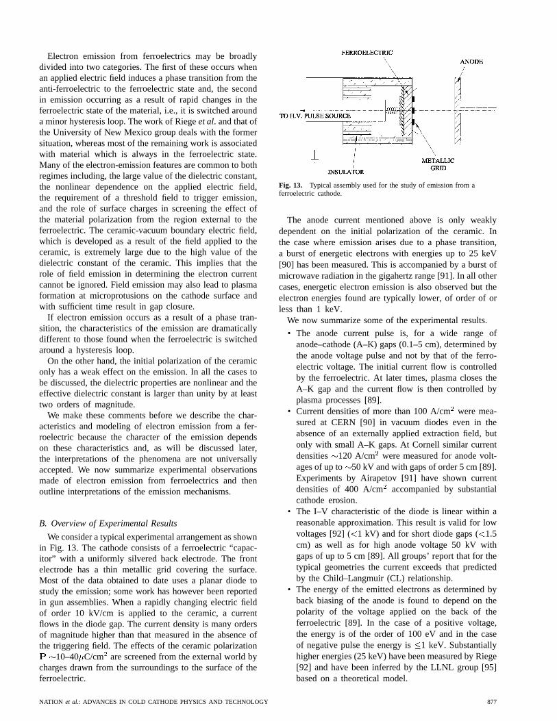
Fig. 14. Schematic illustrating the charge redistribution model.Electrons are repelled from the surface of the ferroelectric andform a potential well in the anode cathode space. The oscillatingelectrons form a medium for the transport of current through thediode.
this redistribution process, one can envision the equilibriumstate as consisting of a deep and steep potential well(delta function) which confines the free electrons thatscreen the polarization field from the external world; thepotential well is located at the surface of the ceramic.When the polarization field is altered by an externallyapplied trigger pulse, the potential well becomes broaderand shallower—in other words the electrons forming thewell redistribute within the A–K gap. This process is shownschematically in Fig. 14, which also includes a sketch ofthe potential distribution due to the redistributed surfaceelectron charge. In zero order the exact distribution of theelectrons is not critical since we can evaluate the potentialwell adequately by solving the Poisson equation for zerovoltage on both the anode and the cathode surfaces. Wealso assume, as seen in experiment with all but the shortestA–K gaps, zero anode current for zero anode voltage. Thepotential in a diode gap is then given by
where is the charge per unit surface repelled into thegap.
The electrons oscillate in the potential well describedabove and their average normalized kinetic energy is givenby , however the netcurrent associated with this motion is zero. When an anodevoltage is applied, the motion of the oscillating electronsis perturbed and a net current flows. The diode impedance
is given by
where is the diode surface area and 377 . Thisimpedance is directly related to the amount of chargerepelled in the gap that in turn depends on the state ofthe ferroelectric. The electrons repelled by the ferroelectricform a medium that facilitates the conduction. The amountof charge that traverses the A–K gap can be much largerthan the initial charge on the surface of the ceramic.This is particularly important when a long anode voltagepulse is applied. The current flow is then due to electronsemitted from the surface of the ceramic by, for example,field emission. This may or may not be accompanied bysignificant plasma formation. A self-consistent solution ofthe equations developed based on this model has pro-vided good quantitative agreement with the experimentaldata, in particular the excess of current beyond the CLlimit, the linear I–V curve, the hysteresis characteristicof the ferroelectric, and the delay pulse experiments. Theagreement holds over variations of more than three ordersof magnitude in the anode voltage and two orders ofmagnitude in the diode gap spacing.
Its results are presented in detail in [89] and partiallyin [99]. The theory is, however, still incomplete since itdoes not explain the microscopic emission process, butrather postulates that a fraction of the excess charge redis-tributes in the gap. In addition, although there is substantialevidence that plasma develops on the surface of the ferro-electric [100], [106]–[106], the plasma effects are ignored.
3) LLNL Model: The CL law includes energy conserva-tion, therefore if the CL limit is exceeded, some additionalenergy must be provided. In the framework of the redistri-bution model, electrostatic energy is coupled into the diodegap. The LLNL group has developed a phenomenologicalmodel [105] based on the assumption that electrons areinjected by the ferroelectric into the A–K gap with aninitial kinetic energy . It was assumed that the injectedcurrent was sufficiently large to cause a virtual cathode tobe formed. When a voltage is applied to the anode thecurrent density is calculated as
where and is the CL limiting currentdensity. This model shows that at low voltagesthe current density may exceed the CL limit whereas at highvoltages the CL limit is asymptotically approached. Basedon their experimental data [95], the authors infer that theinitial kinetic energy of the electrons is approximately 5keV.
4) Mesyats’ Model: In the previous models no attentionwas paid to the processes which occur on the surface of theceramic. In an attempt to explain the excess of the measuredcurrent beyond the CL limit and the short delay between themoment the voltage is applied to trigger the ferroelectric
NATION et al.: ADVANCES IN COLD CATHODE PHYSICS AND TECHNOLOGY 879
and the start of the diode current, Mesyat’s and his co-workers [105], [106] employ a model of explosive electronemission (EEE). The emission is triggered by field en-hancements at triple-points (vacuum-metal-dielectric). Oneof the basic assumptions is that electron emission followsthe Fowler–Nordheim relation but the local field at theemission site is enhanced by the effective dielectric constantat the contact point (with the metal). The local electricfield is sufficiently high to bend the energy bands in thedielectric facilitating electron injection from the Fermi levelof the metal into the conduction band of the dielectric.Latham [107] has shown that this leads to a current flowthrough the dielectric that satisfies an expression similar toFowler–Nordheim. The current flow across the dielectricis not uniform but forms in microchannels of very highcurrent density. This current can contribute directly to theanode current flow and can lead to plasma formation on thesurface of the cathode. According to Mesyat’s [105] plasmapropagates along the front surface of the ceramic with avelocity when a voltage pulse is applied to the backof the sample, i.e., . It was found experimentallythat the coefficient is 500 and 2000 cm/sV for negativeand positive polarity (of the ceramic) respectively. In [106],the authors claim that this phenomena can account for thetime delay between the applied ferroelectric voltage andthe anode current. Other than expanding across the surfaceof the cathode, the plasma propagates toward the anodewith a typical velocity , and the limiting current may beapproximated by
In principle this can explain the excess current in the A–Kgap.
There are, in the author’s view, quantitative difficultieswith this model. Firstly, the experimentally observed expan-sion of the plasma across the surface of the ferroelectricis about one order of magnitude too slow. Secondly, thegap closure velocities required to account for the currentrise time and amplitude are about two orders of magnitudefaster than typical velocities found in pulse power devices[108]. In spite of the difficulties inherent in this model, itraises two important issues which have not been consideredthoroughly in the framework of earlier models. The triple-point emission almost certainly plays an important role inthe emission process [109]. In fact, it has been recentlyshown analytically [110] that a sharp edge attached to a di-electric emits a current which is larger than that foundin the absence of the dielectric. Thus a material having adielectric constant of several thousands might increase theelectron emission from the attached grid by three ordersof magnitude. Furthermore, in [97] there is a very cleardependence between the emitted current and the geometryof the emitting surface. The second important aspect thathas been emphasized by Mesyats is the effect of plasma.When voltage is applied to the back of the ferroelectric,local “sparks” are observed on the gridded surface. This ismost evident when the applied trigger electric field exceeds
25 kV/cm and becomes less evident at the more typical15-kV/cm stress. Therefore it is quite obvious that plasmais present. Recent experiments performed at Cornell [100]with long anode pulses 5 s indicate that for the first 1–2
s the ferroelectric plays the dominant role and after thatthe plasma controls the performance of the diode.
In many of the ferroelectric diode experiments carried outto date, the late time behavior of the diode is determinedby the energy deposition in the anode. The effects causedinclude anode plasma formation and back sputtering of thecathode surface. These effects are not observed in electrongun geometries, where the beam dump is remote fromthe gun. There is almost no data published to date onferroelectric guns, however in our experience the cathodewear is minimal at 200 A and 500 kV. In these geometriesit is also hard to see how plasma motion across the gun oreven an ambipolar like ion drift across the gun can occur.These experiments provide strong evidence in favor of therelevance of an emission based on the charge redistributionmodel. Recently [113], a 500-kV, 200-A electron gunhas been developed using a ferroelectric cathode and ispresently in use in microwave amplifier experiments.
D. Discussion
The operation of a ferroelectric cathode can be modeledwell with the redistribution charge model using the fractionof charge repelled into the gap as a parameter. In orderto determine the latter, one has to investigate closelythe emission process at the surface. As of now, thereis no quantitative theory that can predict the amount ofcharge (and energy) repelled into the gap. According to theexperimental evidence that has accumulated during the lastyears, it seems that electrons are repelled independent of thepolarity of the material. This indicates that according to thepolarity, electrons are “pulled” either from the metal (grid)or from the ferroelectric. The former case is a type of fieldemission enhanced by the effective dielectric constant ofthe ceramic [104], whereas the latter is yet to be explained.
Both effects are probably accompanied by some plasmaformation that may limit the useful pulse length of the e-beam to be generated. However, so far this has not impededthe application of ferroelectric cathodes to various devices.In fact, bearing in mind that the research into ferroelectricemission only began in the late 1980’s at CERN drivenby the need for a reliable high-current electron source foraccelerator applications, its progress has been dramatic.Ferroelectric sources have been proposed in the context ofseveral applications, including high-power radiation sources[92], [93], [95], [100], gated electron-beam devices, flatdisplays [111], and ion sources [112].
In conclusion, the emission from ferroelectric ceramicsis reasonably well understood though there are severalimportant topics which are yet to be determined. Fromthe applications points of view the advantages are clear:extraction of high currents at relatively low electric fields,good brightness, reliable and repetitive pulses, and in otherapplications, where only poor vacuum is available.
880 PROCEEDINGS OF THE IEEE, VOL. 87, NO. 5, MAY 1999
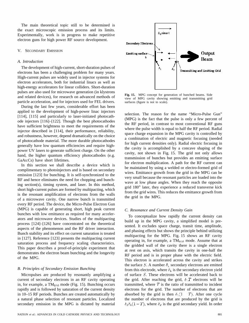
The main theoretical topic still to be determined isthe exact microscopic emission process and its limits.Experimentally, work is in progress to make repetitiveelectron guns for high power RF source development.
V. SECONDARY EMISSION
A. Introduction
The development of high-current, short-duration pulses ofelectrons has been a challenging problem for many years.High-current pulses are widely used in injector systems forelectron accelerators, both for industrial linacs as well ashigh-energy accelerators for linear colliders. Short-durationpulses are also used for microwave generation (in klystronsand related devices), for research on advanced methods ofparticle acceleration, and for injectors used for FEL drivers.
During the last few years, considerable effort has beenapplied to the development of high-power linac injectors[114], [115] and particularly to laser-initiated photocath-ode injectors [116]–[122]. Though the best photocathodeshave sufficient brightness to meet the requirements of theinjector described in [114], their performance, reliability,and robustness, however, depend dramatically on the choiceof photocathode material. The more durable photocathodesgenerally have low quantum efficiencies and require high-power UV lasers to generate sufficient charge. On the otherhand, the higher quantum efficiency photocathodes (e.g.GaAs:Cs) have short lifetimes.
In this section we shall describe a device which iscomplimentary to photoinjectors and is based on secondaryemission [123] for bunching. It is self-synchronized to theRF and hence eliminates the need for chopping and bunch-ing section(s), timing system, and laser. In this method,short high-current pulses are formed by multipacting, whichis the resonant amplification of electrons from the wallsof a microwave cavity. One narrow bunch is transmittedevery RF period. The device, the Micro-Pulse Electron Gun(MPG) is capable of generating short, high peak currentbunches with low emittance as required for many acceler-ators and microwave devices. Studies of the multipactingprocess [124]–[126] have concentrated on the theoreticalaspects of the phenomenon and the RF driver interaction.Bunch stability and its effect on current saturation is treatedin [127]. Reference [123] presents the multipacting currentsaturation process and frequency scaling characteristics.This paper describes a proof-of-principle experiment thatdemonstrates the electron beam bunching and the longevityof the MPG.
B. Principles of Secondary Emission Bunching
Micropulses are produced by resonantly amplifying acurrent of secondary electrons in an RF cavity operatingin, for example, a TM mode (Fig. 15). Bunching occursrapidly and is followed by saturation of the current densityin 10–15 RF periods. Bunches are created automatically bya natural phase selection of resonant particles. Localizedsecondary emission in the MPG is dictated by material
Fig. 15. MPG concept for generation of bunched beams. Sideview of MPG cavity showing emitting and transmitting gridsurfaces (figure is not to scale).
selection. The reason for the name “Micro-Pulse Gun”(MPG) is the fact that the pulse is only a few percent ofthe RF period, in contrast to most conventional RF gunswhere the pulse width is equal to half the RF period. Radialspace charge expansion in the MPG cavity is controlled bya combination of electric and magnetic focusing (neededfor high current densities only). Radial electric focusing inthe cavity is accomplished by a concave shaping of thecavity, not shown in Fig. 15. The grid not only allowstransmission of bunches but provides an emitting surfacefor electron multiplication. A path for the RF current canbe maintained by using a welded or electro-formed grid ofwires. Emittance growth from the grid in the MPG can bevery small because the resonant particles are loaded into thewave at low phase angles. When they reach the oppositegrid 180 later, they experience a reduced transverse kickfrom the grid wires. This reduces the emittance growth fromthe grid in the MPG.
C. Resonance and Current Density Gain
To conceptualize how rapidly the current density canbuild up in the MPG cavity, a simplified model is pre-sented. It excludes space charge, transit time, amplitude,and phasing effects but shows the principle behind utilizingmultipacting for the MPG. Fig. 15 shows an RF cavityoperating in, for example, a TM mode. Assume that atthe gridded wall of the cavity there is a single electronat rest on axis, which transits the cavity in one-half theRF period and is in proper phase with the electric field.This electron is accelerated across the cavity and strikesthe surface . A number secondary electrons are emittedfrom this electrode, where is the secondary electron yieldof surface . These electrons will be accelerated back tothe grid. After reaching the grid, electrons will betransmitted, where is the ratio of transmitted to incidentelectrons for the grid. The number of electrons that areabsorbed by the grid is then . After one cyclethe number of electrons that are produced by the grid is
, where is the grid secondary yield. In order
NATION et al.: ADVANCES IN COLD CATHODE PHYSICS AND TECHNOLOGY 881
Table 3Secondary Emission Coefficient of Some Common Materials
to have a gain in the number of electrons, the number ofsecondaries produced must be greater than one, i.e.,
It is necessary to have enough secondary emission feedbackfrom the combination of the grid and solid wall to have gainor buildup of the current density. The electrons go backand forth between the wall and grid repeatedly, amplifyingthe current during the process. This is analogous to a lasercavity with the grid acting as a partially silvered mirror. Thegain of electrons after RF periods is .If there is a “seed” current density in the cavityinitially, then after RF periods the current density isgiven by
until space charge or cavity loading limits the current. Thecurrent density limit with space charge can be found in[123]. For a very low seed current density a high currentdensity can be achieved in a very short time. For example,if , and A/cm ,then in 15 RF periods A/cm . A grid withcould be a metallic mesh coated with, for example, MgOor GaP (see Table 3).
D. Secondary Electron Emission
The yield or secondary emission coefficient of a surfaceis defined to be the average number of secondary electronsemitted for each incident primary electron. This yield is afunction of the incident energy of the primary electrons.The secondary emission coefficient for all materialsincreases at low primary electron energies, reaches a max-imum at energy , and monotonically decreasesat high energies (see Fig. 16). The maximum in the yieldcurve occurs because at increasing energies the primaryelectron penetrates deeper into the material and scattersmore electrons; however, at sufficiently high energies thescattered electrons are born deeper in the material and areincreasingly unable to escape. Table 3 gives some com-monly used materials with high values of[128]–[132].
An experimentally verified universal yield curve, whichdescribes the number of secondary electrons emitted per pri-mary electron (for primaries that are incident perpendicularto the surface), is given by
where and are the arithmetic mean atomic number andatomic weight, respectively [133]. The secondary emission
Fig. 16. Secondary electron emission yield curve for GaP andMgO.
yield for various materials can be calculated, for example,GaP at 50 keV has(50 keV) . For MgO at 50 keV,(50 keV) . With and (GaP) or
and for MgO, there would be gain, sinceis satisfied (assuming ).
1) High Secondary Emitter Selection:High current den-sity secondary emission of greater than 1500 A/cmhasbeen achieved with doped silicon that is prepared withcesium [134]. However, the emitting surface is easilycontaminated by exposure to O. Several photomultipliers(RCA C31024, RCA C31050, and RCA 8850) are builtwith GaP dynodes. GaP is not sensitive to oxygen but issensitive to water. With very thin coatings on the surfaceof GaP, it can be made to allow secondaries to leave andat the same time prevent contamination. Also, GaP can bedoped to eliminate charge build up. Thus GaP could be anexcellent candidate at high energy (up to 100’s of keV).GaAs is another candidate emitter but is sensitive to O.MgO is a good candidate for lower particle energy (60keV) but would have to be applied in a thin layer in orderto minimize charge build-up.
2) Extraction Grid: The grid can be thought of as ametallic mesh coated with a high secondary electron ma-terial. The grid imposes some limitations on the operatingfrequency, since to behave like a conducting wall in the RFfield, the wire spacing of the grid must be less than an RFwavelength, . Conversely, if the operating frequencyis too large (e.g., 100 GHz), the physical size of the grid(and cavity) will make fabrication difficult.
Grid heating should not be a limitation. Consider amolybdenum grid with a thin coating of secondary emittingmaterial. The average power/unit area, , delivered tothe grid wires is
where and are the macropulse duration and repetitionrate, respectively, is the FWHM of the micropulse current,
is the cavity drive frequency and . Forexample using GHz, cm,
kV, A/cm , ps,kHz and s then W/cm .
882 PROCEEDINGS OF THE IEEE, VOL. 87, NO. 5, MAY 1999
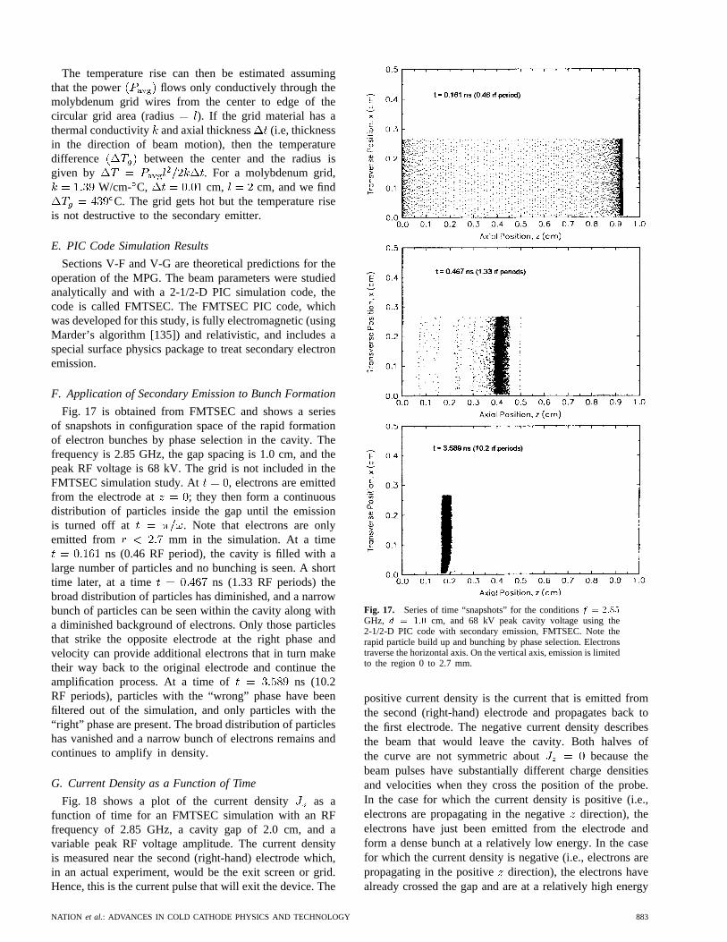
The temperature rise can then be estimated assumingthat the power flows only conductively through themolybdenum grid wires from the center to edge of thecircular grid area (radius ). If the grid material has athermal conductivity and axial thickness (i.e, thicknessin the direction of beam motion), then the temperaturedifference between the center and the radius isgiven by . For a molybdenum grid,
W/cm- C, cm, cm, and we findC. The grid gets hot but the temperature rise
is not destructive to the secondary emitter.
E. PIC Code Simulation Results
Sections V-F and V-G are theoretical predictions for theoperation of the MPG. The beam parameters were studiedanalytically and with a 2-1/2-D PIC simulation code, thecode is called FMTSEC. The FMTSEC PIC code, whichwas developed for this study, is fully electromagnetic (usingMarder’s algorithm [135]) and relativistic, and includes aspecial surface physics package to treat secondary electronemission.
F. Application of Secondary Emission to Bunch Formation
Fig. 17 is obtained from FMTSEC and shows a seriesof snapshots in configuration space of the rapid formationof electron bunches by phase selection in the cavity. Thefrequency is 2.85 GHz, the gap spacing is 1.0 cm, and thepeak RF voltage is 68 kV. The grid is not included in theFMTSEC simulation study. At , electrons are emittedfrom the electrode at ; they then form a continuousdistribution of particles inside the gap until the emissionis turned off at . Note that electrons are onlyemitted from mm in the simulation. At a time
ns (0.46 RF period), the cavity is filled with alarge number of particles and no bunching is seen. A shorttime later, at a time ns (1.33 RF periods) thebroad distribution of particles has diminished, and a narrowbunch of particles can be seen within the cavity along witha diminished background of electrons. Only those particlesthat strike the opposite electrode at the right phase andvelocity can provide additional electrons that in turn maketheir way back to the original electrode and continue theamplification process. At a time of ns (10.2RF periods), particles with the “wrong” phase have beenfiltered out of the simulation, and only particles with the“right” phase are present. The broad distribution of particleshas vanished and a narrow bunch of electrons remains andcontinues to amplify in density.
G. Current Density as a Function of Time
Fig. 18 shows a plot of the current density as afunction of time for an FMTSEC simulation with an RFfrequency of 2.85 GHz, a cavity gap of 2.0 cm, and avariable peak RF voltage amplitude. The current densityis measured near the second (right-hand) electrode which,in an actual experiment, would be the exit screen or grid.Hence, this is the current pulse that will exit the device. The
Fig. 17. Series of time “snapshots” for the conditionsf = 2:85
GHz, d = 1:0 cm, and 68 kV peak cavity voltage using the2-1/2-D PIC code with secondary emission, FMTSEC. Note therapid particle build up and bunching by phase selection. Electronstraverse the horizontal axis. On the vertical axis, emission is limitedto the region 0 to 2.7 mm.
positive current density is the current that is emitted fromthe second (right-hand) electrode and propagates back tothe first electrode. The negative current density describesthe beam that would leave the cavity. Both halves ofthe curve are not symmetric about because thebeam pulses have substantially different charge densitiesand velocities when they cross the position of the probe.In the case for which the current density is positive (i.e.,electrons are propagating in the negativedirection), theelectrons have just been emitted from the electrode andform a dense bunch at a relatively low energy. In the casefor which the current density is negative (i.e., electrons arepropagating in the positive direction), the electrons havealready crossed the gap and are at a relatively high energy
NATION et al.: ADVANCES IN COLD CATHODE PHYSICS AND TECHNOLOGY 883
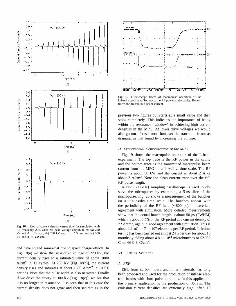
(a)
(b)
(c)
Fig. 18. Plots of current density versus time for simulation withRF frequency 2.85 GHz, for peak voltage amplitude of: (a) 220kV and d = 2:0 cm; (b) 280 kV andd = 2:0 cm; and (c) 300kV and d = 2:0 cm.
and have spread somewhat due to space charge effects. InFig. 18(a) we show that at a drive voltage of 220 kV, thecurrent density rises to a saturated value of about 1000A/cm in 13 cycles. At 280 kV [Fig. 18(b)], the currentdensity rises and saturates at about 1600 A/cmin 10 RFperiods. Note that the pulse width is also narrower. Finallyif we drive the cavity at 300 kV [Fig. 18(c)], we see thatit is no longer in resonance. It is seen that in this case thecurrent density does not grow and then saturate as in the
(a)
(b)
Fig. 19. Oscilloscope traces of macropulse operation of theL-band experiment. Top trace: the RF power in the cavity. Bottomtrace: the transmitted beam current.
previous two figures but starts at a small value and thenstops completely. This indicates the importance of beingwithin the resonance “window” in achieving high currentdensities in the MPG. At lower drive voltages we wouldalso go out of resonance, however the transition is not asdramatic as that found by increasing the voltage.
H. Experimental Demonstration of the MPG
Fig. 19 shows the macropulse operation of the L-bandexperiment. The top trace is the RF power in the cavityand the bottom trace is the transmitted macropulse beamcurrent from the MPG on a 1s/div. time scale. The RFpower is about 50 kW and the current is about 2 A orabout 2 A/cm. Note the clean current trace over the fullRF pulse length.
A fast (50 GHz) sampling oscilloscope is used to ob-serve the micropulses by examining a 5-ns slice of themacropulse. Fig. 20 shows a measurement of the buncheson a 500-ps/div time scale. The bunches appear withthe periodicity of the RF field (800 ps), in excellentagreement with simulation. More detailed measurementsshow that the actual bunch length is about 50 ps (FWHM)which is about 6.5% of the RF period at a current density of22 A/cm , again in good agreement with simulation. This isabout 1.1 nC or 7 10 electrons per RF period. Lifetimetesting has been carried out almost 24 h per day for about 15months, yielding about 4.8 10 microbunches or 52 050C or 66 348 C/cm.
VI. OTHER SOURCES
A. EEE
EEE from carbon fibers and other materials has longbeen proposed and used for the production of intense elec-tron beams with short pulse durations. In this applicationthe primary application is the production of X-rays. Theemission current densities are extremely high, often 10
884 PROCEEDINGS OF THE IEEE, VOL. 87, NO. 5, MAY 1999
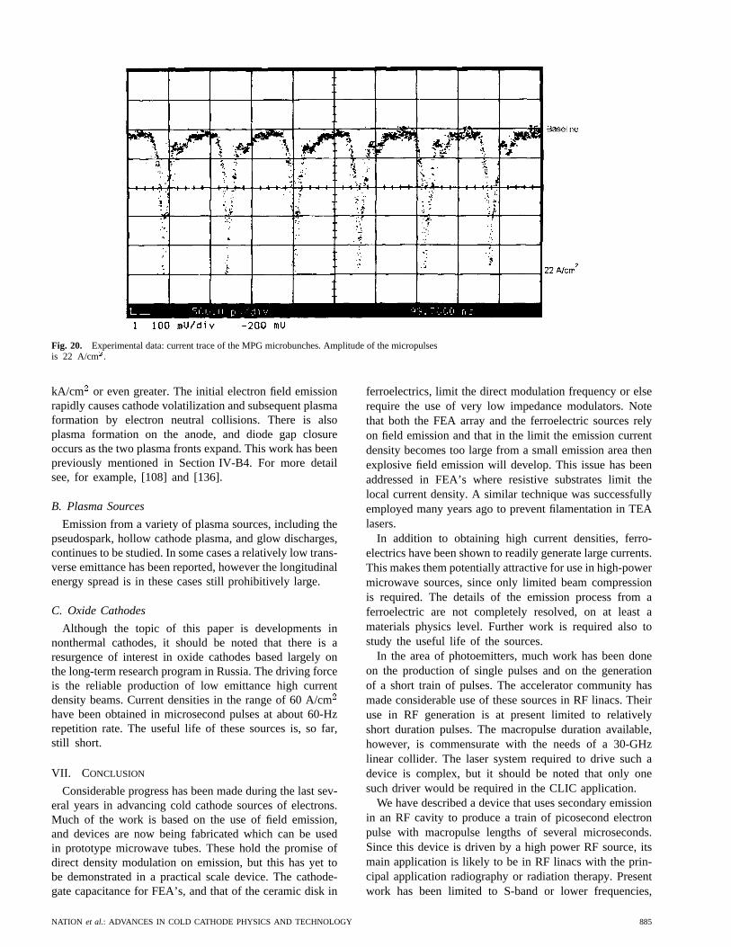
Fig. 20. Experimental data: current trace of the MPG microbunches. Amplitude of the micropulsesis 22 A/cm2.
kA/cm or even greater. The initial electron field emissionrapidly causes cathode volatilization and subsequent plasmaformation by electron neutral collisions. There is alsoplasma formation on the anode, and diode gap closureoccurs as the two plasma fronts expand. This work has beenpreviously mentioned in Section IV-B4. For more detailsee, for example, [108] and [136].
B. Plasma Sources
Emission from a variety of plasma sources, including thepseudospark, hollow cathode plasma, and glow discharges,continues to be studied. In some cases a relatively low trans-verse emittance has been reported, however the longitudinalenergy spread is in these cases still prohibitively large.
C. Oxide Cathodes
Although the topic of this paper is developments innonthermal cathodes, it should be noted that there is aresurgence of interest in oxide cathodes based largely onthe long-term research program in Russia. The driving forceis the reliable production of low emittance high currentdensity beams. Current densities in the range of 60 A/cmhave been obtained in microsecond pulses at about 60-Hzrepetition rate. The useful life of these sources is, so far,still short.
VII. CONCLUSION
Considerable progress has been made during the last sev-eral years in advancing cold cathode sources of electrons.Much of the work is based on the use of field emission,and devices are now being fabricated which can be usedin prototype microwave tubes. These hold the promise ofdirect density modulation on emission, but this has yet tobe demonstrated in a practical scale device. The cathode-gate capacitance for FEA’s, and that of the ceramic disk in
ferroelectrics, limit the direct modulation frequency or elserequire the use of very low impedance modulators. Notethat both the FEA array and the ferroelectric sources relyon field emission and that in the limit the emission currentdensity becomes too large from a small emission area thenexplosive field emission will develop. This issue has beenaddressed in FEA’s where resistive substrates limit thelocal current density. A similar technique was successfullyemployed many years ago to prevent filamentation in TEAlasers.
In addition to obtaining high current densities, ferro-electrics have been shown to readily generate large currents.This makes them potentially attractive for use in high-powermicrowave sources, since only limited beam compressionis required. The details of the emission process from aferroelectric are not completely resolved, on at least amaterials physics level. Further work is required also tostudy the useful life of the sources.
In the area of photoemitters, much work has been doneon the production of single pulses and on the generationof a short train of pulses. The accelerator community hasmade considerable use of these sources in RF linacs. Theiruse in RF generation is at present limited to relativelyshort duration pulses. The macropulse duration available,however, is commensurate with the needs of a 30-GHzlinear collider. The laser system required to drive such adevice is complex, but it should be noted that only onesuch driver would be required in the CLIC application.
We have described a device that uses secondary emissionin an RF cavity to produce a train of picosecond electronpulse with macropulse lengths of several microseconds.Since this device is driven by a high power RF source, itsmain application is likely to be in RF linacs with the prin-cipal application radiography or radiation therapy. Presentwork has been limited to S-band or lower frequencies,
NATION et al.: ADVANCES IN COLD CATHODE PHYSICS AND TECHNOLOGY 885
although scaling studies have been carried out indicatingthat higher frequency operation is possible. It may bepossible to use the bunches generated by this processand postaccelerate the electrons to produce amplified RFpower or power at a harmonic of the bunching frequency.The latter technique is similar to that used in the CLICexperiments described in Section III-D.
Although research into new electron emitters has ad-vanced substantially in the last several years, the use ofthese novel emitters, and others not described in this paper,still has a considerable way to go before their use inmicrowave tubes becomes widespread. Present limitationsinclude explosive field emission and plasma formation athigh current densities. The ability to turn on emissionquickly from a cold cathode device and to profile theemission characteristics both temporally and spatially offersa strong incentive to pursue this work further. Finally, wenote that there are a number of applications where lifetimeis not a major consideration, in which case these newsources may be used at their present state of development.
REFERENCES
[1] H. Makishima, H. Imura, M. Takahashi, H. Fukui, and A.Okamuoto, “Remarkable improvements of microwave electrontubes through the development of the cathode material,” inTech.Dig. IVMC’97, Kyongju, Korea, 1997, pp. 194–199.
[2] H. Imura, S. Tsuida, M. Takahasi, A. Okamoto, H. Makishima,and S. Miyano, “Electron gun design for traveling wave tubes(TWT’s) using a field emitter array (FEA) cathode,” inTech.Dig. IEDM, Int. Electron Devices Meeting, Washington, DC,Dec. 7–10, 1997, pp. 721–724.
[3] H. Takemura, Y. Tomihari, N. Furutake, F. Matsuno, M.Yoshiki, N. Takada, A. Okamoto, and S. Miyano, “A novelvertical current limiter fabricated with a deep trench formingtechnology for highly reliable field emitter arrays,” inTech.Dig. IEDM, Int. Electron Devices Meeting, Washington, DC,Dec. 7–10, 1997, pp. 709–712.
[4] J. Dayton, M. A. Hollis, K. L. Jensen, R. A. Murphy, L.Parameswaran, and E. Wintucky, private communications.
[5] S. G. Bandy, M. C. Green, C. A. Spindt, M. A. Hollis, D.Palmer, B. Goplen, and E. G. Wintucky, “Application of gatedfield emitter arrays in microwave amplifier tubes,” in1997 IEEEInt. Conf. Plasma Science, Conf. Record-Abstr., San Diego, May19–22, 1997, p. 127.
[6] L. Parameswaran, R. A. Murphy, C. T. Harris, R. H. Mathews,C. A. Graves, M. A. Hollis, J. Shaw, M. A. Kodis, M. Garven,M. T. Ngo, K. L. Jensen, M. Green, J. Legarra, J. Atkinson,L. Garbini, and S. Bandy, “Field emitter arrays for inductiveoutput amplifiers,” submitted for publication.
[7] K. L. Jensen, J. E. Yater, E. G. Zaidman, M. A. Kodis, and A.Shih, “Advanced emitters for next generation RF amplifiers,”in Tech. Dig. IVMC’97, Kyongju, Korea, 1997, pp. 186–189.
[8] D. Palmer, H. F. Gray, J. Mancusi, D. Temple, C. Ball, J. L.Shaw, and G. E. McGuire, “Silicon field emitter arrays withlow capacitance and improved transconductance for microwaveamplifier applications,”J. Vac. Sci. Technol. B, vol. 13, pp.576–579, 1995.
[9] R. K. Parker, K. L. Jensen, and R. H. Abrams, “Field emitterarray development for high frequency applications,” inTech.Dig. IVMC’97, Kyongju, Korea, 1997, pp. 92–97.
[10] C. A. Spindt, C. E. Holland, P. R. Schwoebel, and I. Brodie,“Field-Emitter array development for microwave applications,”J. Vac. Sci. Technol. B, vol. 14, pp. 1986–1989, 1996.
[11] C. A. Spindt, C. E. Holland, P. R. Schwoebel, and I. Brodie,“Field-emitter array development for microwave applications(II),” in Tech. Dig. IVMC’97, Kyongju, Korea, 1997, pp.200–207.
[12] C. O. Bozler, C. T. Harris, S. Rabe, D. D. Rathman, M. A.Hollis, and H. I. Smith, “Array of gated field-emitter cones
having 0.32 m tip-to-tip spacing,”J. Vac. Sci. Technol. B, vol.12, pp. 629–632, 1994.
[13] C. O. Bozler, D. D. Rathman, C. T. Harris, G. A. Lincoln, C.A. Graves, R. H. Mathews, S. Rabe, R. A. Murphy, and M.A. Hollis, “Field-emitter arrays for microwave power tubes,”in MPTC’96 Proc..
[14] J. P. Calame, H. F. Gray, and J. L. Shaw, “Analysis anddesign of microwave amplifiers employing field-emitter arrays,”J. Appl. Phys., vol. 73, pp. 1485–1504, 1993.
[15] H. G. Kosmahl, “A wide-bandwidth high gain small-size dis-tributed amplifier with field-emission triodes (FETRODE’s) forthe 10 to 300 GHz frequency range,”IEEE Trans. ElectronDevices, vol. 36, pp. 2728–2737, 1989.
[16] C. A. Spindt, “A thin film field-emission cathode,”J. Appl.Phys., vol. 39, pp. 3504–3505, 1968.
[17] H. F. Gray, “Silicon field emitter array technology,” inProc.29th Int. Field Emission Symp., Goteborg, Sweden, Aug. 9–13,1982, pp. 111–118.
[18] W. A. Mackie, R. L. Hartman, and P. R. Davis, “High currentdensity field-emission from transition metal carbides,”Appl.Surface Sci., vol. 67, pp. 29–35, 1993.
[19] W. A. Mackie, R. L. Hartman, M. A. Anderson, and P. R. Davis,“Transition metal carbides for use as field-emission cathodes,”J. Vac. Sci. Technol. B, vol. 12, pp. 722–726, 1994.
[20] H. F. Gray, “The field-emitter display,”Inform. Display, vol.9, no. 3, pp. 8–14, 1993.
[21] D. Cathey, Jr., “Field-Emission displays,”Inform. Display, vol.11, pp. 16–20, 1995.
[22] K. Derbyshire, “Beyond AMLCDs: Field emission displays,”Solid State Technol., vol. 37, no. 11, pp. 55–65, 1994.
[23] B. R. Chalamala, Y. Wei, and B. E. Gnade, “FED up with fattubes,” IEEE Spectrum, vol. 35, pp. 42–51, Apr. 1998.
[24] V. T. Binh, N. Garcia, and S. T. Purcell, “Electron field-emission from atomic-sources: Fabrication, properties and ap-plications of nanotips,”Adv. Imaging and Electron Phys., vol.95, pp. 63–153, 1996.
[25] R. H. Fowler and L. W. Nordheim, “Electron emission inintense fields,”Proc. Roy. Soc. A, vol. 119, pp. 173–181, 1928.
[26] I. Brodie and P. R. Schwoebel, “Vacuum microelectronic de-vices,” Proc. IEEE, vol. 82, pp. 1006–1034, 1994.
[27] F. Charbonnier, “Arcing and voltage breakdown in vacuummicroelectronics microwave devices using field emitter arrayscauses and possible solutions,” inTech. Dig. IVMC’97, Ky-ongju, Korea, 1997, pp. 7–13.
[28] W. A. Mackie, private communication.[29] T. Xie, W. A. Mackie, and P. R. Davis, “Field emission from
ZrC films on Si and Mo single emitters and emitter arrays,”J.Vac. Sci. Technol. B, vol. 14, p. 2090, 1996.
[30] D. Temple, C. A. Ball, W. D. Palmer, L. N. Yadon, D. Vellenga,J. Mancusi, G. E. McGuire, and H. F. Gray, “Fabrication ofcolumn-based silicon field emitter errays for enhanced perfor-mance and yield,”J. Vac. Sci. Technol. B, vol. 13, pp. 150–157,1995.
[31] L. N. Yadon, D. Temple, W. D. Palmer, C. A. Ball, G. E.McGuire, C. M. Tang, and T. A. Swy den, “Mini-columnsilicon field-emitter arrays,”J. Vac. Sci. Technol. B, vol. 13,pp. 580–584, 1995.
[32] A. I. Akinwande, P. E. Bauhahn, H. F. Gray, T. R. Ohstein,and J. O. Holmen, “Nanometer scale thin-film edge emitter de-vices with high current density characteristics,” inInt. ElectronDevices Meeting Tech. Dig., 1992, pp. 367–371.
[33] C. M. Tang, M. Goldstein, T. A. Swyden, and J. E. Walsh, “Freeelectron micro-laser,”Nucl. Instrum. Methods A, vol. 358, pp.7–10, 1995.
[34] Y. Liu and Y. Y. Lau, “An evaluation of the intrinsic emit-tance of a field emitter,”J. Vac. Sci. Technol. B, vol. 14, pp.2126–2129, 1996.
[35] C. M. Tang, “Microelectronic cathodes for RF sources andaccelerator applications,” inProc. 1995 Particle AcceleratorConf., Dallas, TX, 1995, pp. 70–74.
[36] C. M. Tang and T. A. Swyden, “Beam collimiation fromfield-emitter arrays with linear planar lenses,” inSociety forInformation Display Int. Symp. Dig. Tech. Papers, 1997, vol.XXVIII, pp. 115–118.
[37] C. A. Brau, “High-brightness electron beams-small free-electronlasers,” presented at 19th Interntional Free Electron LaserConference, Beijing, China, Aug. 1997.
886 PROCEEDINGS OF THE IEEE, VOL. 87, NO. 5, MAY 1999
[38] , “Needle cathodes as sources of high-brightness electronbeams,” presented at Gargnano Electron Beam Workshop, 1997.
[39] C. A. Brau, private communication.[40] P. R. Schwoebel and I. Brodie, “Surface-science aspects of
vacuum microelectronics,”J. Vac. Sci. Technol. B, vol. 13, pp.1391–1410, 1995.
[41] I. Brodie and C. A. Spindt,Adv. Electron. Electron Phys., vol.83, pp. 1–106, 1992.
[42] A. Ting, C. M. Tang, T. A. Swyden, D. McCarthy, andM. Peckerar, “Field-effect controlled vacuum field-emissioncathodes,” inTech. Dig. IVMC’91, 1991, pp. 200–201.
[43] J. Itoh, T. Hirano, and S. Kanemaru, “Ultrastable emission froma metal-oxide-semiconductor field-effect transistor-structuredSi emitter tip,” Appl. Phys. Lett., vol. 69, pp. 1578–1579,1996.
[44] K. Koga, S. Kanemaru, and J. Itoh, “Low voltage operationfrom tower structure MOSFET Si field emitter,” in1998 Tech.Dig. Intl. Vacuum Microelectronics Conf., 1998, pp. 126–127.
[45] K. Yokoo, M. Arai, M. Mori, J. E. Bae, and S. Ono, “Activecontrol of the emission current of field emitter arrays,”J. Vac.Sci. Technol. B, vol. 13, pp. 491–493, 1995.
[46] P. M. McIntyre, H. M. Bizek, S. M. Elliott, A. Nassiri, M.B. Popovic, D. Pararia, C. A. Swenson, and H. F. Gray,IEEETrans. Electron Devices, vol. 36, p. 2720, 1989.
[47] C. M. Tang, Y. Y. Lau, and T. A. Swyden, “Deflectionmicrowave amplifier with field-emitter arrays,”Appl. Phys.Lett., vol. 65, pp. 2881–2883, 1994.
[48] J. Zhou, C. Huang, C. Shi, M. Murnane, and H. C. Kapteyu“Generation of 21 fs multijoule energy pulses by use ofTi:sapphire,”Opt. Lett., vol. 19, no. 2, pp. 126–128, 1994.
[49] C. P. J. Barty, C. I. Gordon III, and B. E. Lemoff, “Multiter-awatt 30 fs Ti:sapphire laser system,”Opt. Lett., vol. 18, pp.1442–1444, 1994.
[50] J. P. Heritage, A. M. Weinerand, and R. N. Thurston, “Picosec-ond pulse shaping by spectral phase and amplitude manipula-tion,” Opt. Lett., vol. 10, p. 609, 1985.
[51] A. M. Weiner, J. P. Heritage, and E. M. Kirschner, “Highresolution femtosecond pulse shaping,”J. Opt. Soc. Amer. B,vol. 5, p. 1563, 1988.
[52] S. Skupsky, T. J. Kessler, S. A. Letzring, and Y. H. Chuang,“Laser beam shaping using spectral beam deflection,”J. Appl.Phys., vol. 73, pp. 2678–2684, 1993.
[53] R. P. Scott, C. V. Bennett, and B. H. Kolner, “Picosecond lasersource with single knob adjustable pulse width,” inProc. Lasersfor RF Guns, Anaheim, CA, May 14–15, 1994, BNL-52435,1994, pp. 97–108.
[54] L. K. Cotter and M. A. Handschy, “High contrast ferroelectricliquid crystal spatial light modulator,”Opt. Lett., vol. 19, pp.1255–1256, 1994.
[55] G. P. Le Sage, H. X. C. Feng, L. L. Laurent, F. V. Hartemann,N. C. Luhmann, Jr., J. P. Heritage, S. N. Fochs, M. D. Perry,and G. A. Westenskow, “Theory and design of a photoinjector-driven chirped pulse free-electron maser,”IEEE Trans. PlasmaSci., vol. 24, pp. 781–795, 1996.
[56] The CLIC Study Group, “CTF2 design report,” CERN, Geneva,Switzerland, CERN Rep. CLIC Note No. 304, 1996.
[57] M. A. LaPointe, R. B. Yoder, M. Wang, A. K. Ganguly, C.Wang, B. Hafizi, and J. L. Hirshfield, “High-power microwaveproduction by gyroharmonic conversion and co-generation,”in Proc. Advanced Accelerator Concepts Workshop, AIP Conf.Proc. 398, 1997, p. 887.
[58] D. B. Hopkins, K. Halbach, E. H. Hoyer, A. M. Sessler, and E.J. Sternbach, “Elements of a realistic 17 GHz FEL/TAB design,”AIP Conf. Proc. 193, 1989, p. 141.
[59] R. H. Fowler, “The analysis of photoelectric sensitivity curvesfor clean metals at various temperatures,”Phys. Rev., vol. 38,pp. 45–56, 1931.
[60] T. Srinivasan-Rao, J. Fischer, and T. Tsang, “Photoemissionstudies on metals using picosecond ultraviolet laser pulses,”J.Appl. Phys., vol. 69, pp. 3291–3296, 1991.
[61] E. Chevallay, J. Durand, S. Hutchins, G. Suberlucq, and M.Wurgel, “Photocathodes tested in the dc gun of the CERNphotoemission laboratory,”Nucl. Instrum. Meth. Phys. Res. A,vol. 340, pp. 146–156, 1994.
[62] T. Srinivasan-Rao, J. Yu, and X. J. Wang, “Study on thesensitivity of quantum efficiency of copper photocathodes onsample preparation,” Brookhaven National Lab., Rep. 62626,1996.
[63] T. Srinivasan-Rao, J. Fischer, and T. Tsang, “Picosecond fieldassisted photoemission from yttrium microstructures,”J. Opt.Soc. Am., vol. B8, pp. 294–299, 1991.
[64] , “Optical field enhanced multiphoton photoemission incopper mirrors,”Appl. Phys. Lett., vol. 63, 1595–1597, 1993.
[65] , “Photoemission from Mg irradiated by short pulse ultra-violet and visible lasers,”J. Appl. Phys., vol. 77, pp. 1275–1279,1995.
[66] G. Suberlucq, “Development and production of photocathodesfor the CLIC test facility,” inProc. 18th Int. Free Electron Conf.,Rome, Italy, Aug. 1996, pp. 20–30.
[67] T. Srinivasan-Rao, I. Ben-Zvi, J. Smedley, X. J. Wang, and M.Woodle, “Performance of magnesium cathode in the S band RFgun,” in Proc. Particle Accelerator Conf., Vancouver, Canada,May 1997, pp. 12–16.
[68] X. J. Wang, M. Babzein, K. Batchelor, I. Ben-Zui, R. Mal-one, I. Pogorelsky, X. Qui, J. Sheehan, J. Skaritka, and T.Srinivasan-Rao, “Experimental characterization of the high-brightness electron photoinjector,”Nucl. Instrum. Meth. Phys.Res. A, vol. 375, pp. 82–86, 1996.
[69] J. Rosenzweig, N. Barovet al., “Initial measurements of theUCLA RF photoinjector,”Nucl. Instrum. Meth. Phys. Res. A,vol. 341, pp. 379–385, 1994.
[70] S. Trotz, W. Brown, B. Danly, J. P. Hogge, K. E. Kreischer,M. Shapiro, and R. J. Temkin, “Experimental operation of a17 GHz photocathode rf gun,” inParticle Accelerator Conf.,Vancouver, Canada, May 1997, pp. 12–16.
[71] B. Leblond, G. Kuznetsov, and M. Batazova, “Short pulse pho-toemission from LaB6-based materials,”Nucl. Instrum. Meth.Phys. Res. A, vol. 372, pp. 562–566, 1996.
[72] I. S. Lehrman, J. Krishnaswamy, R. A. Hartley, and R. Bo-hanick, “Status of the Grumman compact infrared FEL,”Nucl.Instrum. Meth. Phys. Res. A, vol. 358, pp. ABS5–ABS6, 1995.
[73] R. Engstrom,Photomultiplier Handbook, RCA Corp., Lan-caster, PA, 1980, p. 15.
[74] A. di Bona, F. Sabary, S. Valeri, P. Michelato, D. Sertore, and G.Suberlucq, “Auger and X-ray photemission spectroscopy studyon Cs2Te photocathode,”J. Appl. Phys., vol. 80, pp. 3024–3030,1996.
[75] R. Bossart, H. Braun, M. Dehler, and J. C. Godot, “A 3 GHzphotoelectron gun for high beam intensity,” CERN, Geneva,Switzerland, Rep. CLIC Note 297, 1996.
[76] S. H. Kong, D. C. Nguyen, R. L. Sheffield, and B. A. Sherwood,“Fabrication and characterization of cesium telluride photocath-odes: A promising electron source for the Los Alamos advancedFEL,” Nucl. Instrum. Meth. Phys. Res. A, vol. 358, pp. 276–279,1995.
[77] R. Calabrese, G. Ciullo, G. Della Mea, G. P. Egeni, V. Guidi,G. Lamanna, P. Lenisa, B. Maciga, V. Rigato, V. Rudello, L.Tecchio, B. Yang, and S. Zandolin, “Performance of a GaAselectron source,”Nucl. Instrum. Meth. Phys Res. A, vol. 340,pp. 109–113, 1994.
[78] A. V. Aleksandrov, M. S. Avilov, R. Calabrese, G. Ciullo,N. S. Dikansky, V. Guidi, G. Lamanna, P. Logachov, A. V.Novohatsky, L. Tecchio, and B. Yang, “Experimental study ofthe response time of GaAs as a photoemitter,”Phys. Rev. E51,pp. 1449–1452, 1995.
[79] K. Aulenbacher, R. Bossart, H. Braun, J. Clendenin, J. P. Dela-haye, J. Madden, G. Mulhollan, J. Sheppard, G. Suberlucq, andH. Tang, “RF guns and the production of polarized electrons,”CERN, Geneva, Switzerland, Rep. CLIC Note No. 303, 1996.
[80] C. Travier, “An introduction to photo-injector design,”Nucl.Instrum. Meth. Phys. Res. A, vol. 340, pp. 26–39, 1994.
[81] I. Ben-Zvi, “Recent progress in photoinjectors,” inAIP Conf.Proc. No. 398, New York, 1997, pp. 40–54.
[82] A. M. Sessler, “The free electron laser as a power source fora high-gradient accelerating structure,” inAIP Conf. Proc. No.91, New York, 1982, pp. 154–159.
[83] W. Schnell, “Radio-frequency acceleration for linear colliders,”in AIP Conf. Proc. No. 156, New York, 1982, pp. 17–36.
[84] D. C. Nguyen, R. H. Austin,et al. “Initial performance ofLos Alamos advanced free electron laser,”Nucl. Instrum. Meth.Phys. Res. A, vol. 341, pp. 29–33, 1994.
[85] A. di Bona, F. Sabary, S. Joly, P. Michelato, D. Sertore, C.Pagani, and S. Valeri, “Development, operation and analysisof bialkali antimonide photocathodes for high brightness pho-toinjectors,” Nucl. Instrum. Meth. in Phys. Res. A, vol. 385,1997.
NATION et al.: ADVANCES IN COLD CATHODE PHYSICS AND TECHNOLOGY 887
[86] C. P. Beetz, B. Lincoln, K. Segall, D. Wall, M. Vasas, D. R.Winn, D. Doering, and D. Carroll, “Applications of diamondfilms to photocathode electron guns and accelerators,” inExt.Abstr. IEEE Particle Accelerator Conf., San Francisco, CA,May 1991.
[87] W. Gai, M. Conde, R. Konecny, X. Li, J. Power, P. Schoessow,and J. Simpson, “The argonne wakefield accelerator: Diagnos-tics and beam characterization,” inParticle Accelerator Conf.,Vancouver, Canada, May 1997, pp. 12–16.
[88] J. Krishnaswamy, I. S. Lehrman, R. A. Hartley, M. F. Reusch,A. M. M. Todd, R. H. Austin, and D. Feldman, “Beam diag-nostics and modeling in CIRFEL,”Nucl. Instrum. Meth. Phys.Res. A, pp. 119–122, 1996.
[89] G. I. Rosenman, V. A. Okhapkin, Y. L. Chepelev, and V. Y.Shur, “Electron emission during the switching of ferroelectriclead-germanate,”JETP Lett., vol. 39, p. 477, 1984.
[90] H. Gundel, H. Riege, E. J. N. Wilson, J. Handerek, and K.Zioutas, “Fast polarization changes in ferroelectrics and theirapplication in accelerators,”Nucl. Instrum. Methods Phys. Res.A, vol. 280, p. 1, 1989.
[91] A. S. Airapetov, A. K. Krasnykh, I. V. Levshin, and A. Y.Nikitskii, “Measurement of the emission current accompanyingthe reversal of polarization of a ferroelectric,”Sov. Tech. Phys.Lett., vol. 35, p. 182, 1990.
[92] J. D. Ivers, L. Schachter, J. A. Nation, G. S. Kerslick, and R.Advani, “Electron beam using ferroelectric cathodes,”J. Appl.Phys., vol. 73, p. 2667, 1993.
[93] L. Schachter, J. D. Ivers, G. S. Kerslick, and J. A. Nation, “Theanalysis of a diode with a ferroelectric cathode,”J. Appl. Phys.,vol. 73, p. 8097, 1993.
[94] B. Jiang, G. Kirkman, and N. Reinhardt, “High brightnesselectron beam produced by a ferroelectric cathode,”Appl. Phys.Lett., vol. 66, no. 1196, 1995.
[95] S. E. Sampayan, G. J. Caporaso, C. L. Holmes, E. J. Lauer,D. Prosnitz, D. O. Trimble, and G. A. Westenskow, “Emissionfrom ferroelectric cathodes,”Nucl. Instrum. Meth. Phys. Res. A,vol. 340, no. 90, 1994.
[96] T. C. Cavazos, W. L. Wilbanks, C. B. Fleddermann, and D.A. Shiffler, “Repeatable electron emission from (Pb, La)(Zr,Ti) O3 ferroelectric cathodes using direct-current reset,”Appl.Phys. Lett., vol. 65, p. 2612, 1994.
[97] M. Okuyama, J. Asano, and Y. Hamakawa, “Electron emissionfrom lead-zirconate-titanate ferroelectric ceramic induced bypulse electric field,”Japan J. Appl. Phys., vol. 33, p. 5506,1994.
[98] H. Riege, “Electron emission from ferroelectrics—A review,”Nucl. Instrum. Meth. Phys. Res. A, vol. 340, p. 80, 1994.
[99] D. Flechtner, C. Golkowski, G. S. Kerslick, J. A. Nation, andL. Schachter, “Electron emission from lead-zirconate-titanate(PZT) ceramics,”J. Appl. Phys., vol. 83, no. 2, pp. 955–961,Jan. 1998.
[100] D. Flechtner, J. D. Ivers, G. S. Kerslick, J. A. Nation, andL. Schachter, “Ferroelectric electron beam sources,” inProc.Beams’94, 1994, vol. 11, pp. 487–490.
[101] K. Geissler, A. Meineke, H. Riege, J. Handerek, H. Granzer,and D. Suchland, “Enhancement of laser-induced electronemission from ferroelectrics by surface charge refresh-ment,” Nucl. Instrum. Meth. Phys. Res. A, vol. 166, no. 84,1992.
[102] K. Geissler, A. Meineke, H. Riege, K. Schmidt, and J. Han-derek, “Intense laser-induced self-emission of electrons fromferroelectrics by surface charge refreshment,”Nucl. Instrum.Meth. Phys. Res. A, vol. 176, p. 387, 1993.
[103] H. Gundel, “Electron emission from ferroelectrics,” inScienceand Technology of Electroceramic Thin Films, O. Aucielloand R. Waser, Eds. Norwell, MA: Kluwer, 1995, pp. 335–351.
[104] V. D. Kugel, G. Rosenman, D. Shur, and Y. E. Krasik, “Copiouselectron emission from triglycine-sulfate ferroelectric crystal,”J. Appl. Phys., vol. 78, p. 2248, 1995.
[105] G. A. Mesyats “Electron emission from ferroelectric ceramic,”Tech. Phys. Lett., vol. 20, no. 8, 1994.
[106] V. L. Puchkarev and G. A. Mesyats, “On the mechanism ofemission from the ferroelectric ceramic cathode,”J. Appl. Phys.,vol. 78, p. 5633, 1995.
[107] R. V. Latham, “The origin of prebreakdown electron emissionfrom vacuum-insulated high voltage electrodes,”Vacuum, vol.32, p. 137, 1982.
[108] R. K. Parker, R. E. Anderson, and C. V. Duncan, “Plasma-induced field emission and the characteristics of high-currentrelativistic electron flow,”J. Appl. Phys., vol. 45, p. 2463, 1974.
[109] G. A. Mesyats, “Physics of electron emission from metal-dielectric cathodes,”IEEE Trans. Dielectrics Elect. Insulation,vol. 2, p. 272, 1995.
[110] L. Schachter, “Analytic expression for triple-point electronemission from an ideal edge,”Appl. Phys. Lett., vol. 72, no.4, pp. 421–423, 1998.
[111] A. Skilar, “Ferroelectric electron emission flat panel display,”J. Appl. Phys., vol. 79, p. 7401, 1996.
[112] G. Rosenman and M. Urbach, “Ion emission from ferroelectricmedia,” J. Appl. Phys., vol. 72, p. 1952, 1992.
[113] J. D. Ivers, D. Flechtner, C. Golkowski, G. Liu, J. A. Nation,and L. Schachter, “Electron beam generation using a ferroelec-tric cathode,”IEEE Trans. Plasma Sci., to be published.
[114] J. L. Adamski, W. J. Gallagher, R. C. Kennedy, B. Robinson,D. R. Shoffstall, E. L. Tyson, A. M. Vetter, and A. D. Yeremian,“The boeing 120 MeV RF linac for FEL research,”IEEE Trans.Nucl. Sci., vol. NS-32, p. 3397, Oct. 1985.
[115] T. F. Godlove and P. Sprangle, “High-Power free-electron lasersdriven by RF linear accelerators,”Particle Accelerators, vol.34, no. 169, 1990.
[116] M. E. Jones and W. Peter, “Particle-in-cell simulations of thelasertron,” IEEE Trans. Nucl. Sci., vol. NS-32, p. 1794, Oct.1985.
[117] P. Schoessow, E. Chojnacki, W. Gai, C. Ho, R. Konecny, S.Mtingwa, J. Norem, M. Rosing, and J. Simpson, “The argonnewakefield accelerator,” inProc. 2nd Europ. Particle AcceleratorConf., 1990, vol. 606.
[118] K. Batchelor, I. Ben-Zui, R. C. Fernow, J. Fischer, A. S.Fisher, J. Gallardo, G. Ingold, H. G. Kirk, K. P. Leung,R. Malone, I. Pogorelsky, T. Srinivasan-Rao, J. Rogers, T.Tsang, J. Sheehan, S. Ule, M. Woodle, J. Xie, R. S. Zhang,L. Y. Lin, K. T. Mcdonald, D. P. Russell, C. M. Huang,and K. J. Wang, “Performance of Brookhaven photo-cathodeRF gun,” Nucl. Instrum. Meth. Phys. Res., vol. A318, p. 372,1992.
[119] S. C. Hartman, N. Barov, S. Park, C. Pellegrini, J. Rosen-zweig, G. Travish, R. Zhang, P. Davis, C. Joshi, and G.Hairapetian, “Emittance measurements of the 4.5 MeV UCLARF photo-injector,” inProc. Particle Accelerator Conf., 1993,pp. 561–563.
[120] I. Ben-Zvi, “Performance of photocathode RF gun electronaccelerators,” inProc. Part. Accel. Conf., 1993, p. 2962.
[121] I. S. Lehrman, I. A. Birnbaum, M. Cole, R. L. Heuer, andE. Sheedy, “Design and construction of a high-duty factorphotocathode electron gun,” inProc. Particle Accelerator Conf.,1993, vol. 3012.
[122] C. Travier, M. Bernard, P. Dufresne, G. Mihaud, M. Omeich,M. Roch, and J. Rodier, “CANDELA photo-injector high-powertest,” Nucl. Instrum. Meth. Phys. Res. B89, p. 27, 1994.
[123] F. Mako and W. Peter, “A high-current micro-pulse electrongun,” in Proc. Particle Accelerator Conf., 1993, p. 2702.
[124] A. S. Gilmore, Microwave Tubes. Norwood, MA: ArtechHouse, 1986, p. 474.
[125] J. R. M. Vaughan, “Multipactor,”IEEE Trans. Electron Devices,vol. 35, p. 1172, July 1988.
[126] R. Kishek and Y. Y. Lau, “Interaction of multipactor dischargeand RF circuit,”Phys. Rev. Lett., vol. 75, no. 6, p. 1218, 1995.
[127] S. Ryopoulos, D. Chernin, and D. Dialetis, “Theory of electronmultipactor in crossed fields,”Phys. Plasmas, vol. 2, no. 8, p.3194, 1995; also appears inIEEE Trans. Electron Devices, vol.44, p. 489, 1997.
[128] D. E. Gray, Ed.,American Institute of Physics Handbook, 3rded. New York: McGraw-Hill.
[129] E. L. Garwin, F. K. King, R. E. Kirby, and O. Aita, “Surfaceproperties of metal-nitride and metal-carbide films deposited onNb for radio-frequency superconductivity,”J. Appl. Phys., vol.61, no. 3, p. 1145, 1987.
[130] E. L. Garwin, E. W. Hoyt, R. E. Kirby, and T. Momose,“Secondary electron yield and auger electron spectroscopymeasurements on oxides, carbide, and nitride of niobium,”J.Appl. Phys., vol. 59, no. 9, p. 3245, 1986.
[131] A. R. Nyaiesh, E. L. Garwin, F. K. King, and R. E. Kirby,“Properties of thin antimultipactor TiN and Cr2O3 coatingsfor klystron windows,” J. Vac. Sci. Tech. A, vol. 4, p. 2356,1986.
888 PROCEEDINGS OF THE IEEE, VOL. 87, NO. 5, MAY 1999
[132] S. Michizono, A. Kinbara, Y. Saito, S. Yamaguchi, S. Anami,and N. Matuda, “TiN film coatings on alumina radio frequencywindows,” J. Vac. Sci. Tech. A, vol. 10, p. 1180, 1992.
[133] B. K. Agarwal, “Variation of secondary emission with primaryelectron energy,”Proc. Roy. Soc. 71, p. 851, 1958.
[134] G. G. P. van Gorkom and A. M. E. Hoeberechts, “An efficientsilicon cold cathode for high current densities,”Phillips J. Res.,vol. 41, no. 4, p. 343, 1986; alsoJ. Vac. Sci. Tech. B, vol. 4,p. 108, 1986.
[135] B. Marder, “A method for incorporating gauss’ law into elec-tromagnetic PIC codes,”J. Computational Phys., vol. 68, p. 48,1987.
[136] S. P. Bugaev and G. A. Mesyats, “Investigation of the pulsedbreakdown mechanism at the surface of a dielectric in vacuum-1uniform field,” Sov. Phys.-Tech. Phys., vol. 12, pp. 1358–1363,1968.
John A. Nation (Fellow, IEEE) received theBachelor’s and Doctoral degrees in physics fromImperial College, University of London, U.K.
Between 1960 and 1965, he worked at theCNEN Laboratories, Frascati, Italy, and for theCEGB, Leatherhead, U.K. Since 1965, he hasbeen at Cornell University, Ithaca, NY, wherehe is now Professor of Electrical Engineering.From 1984 to 1989, he served as Director of theSchool of Electrical Engineering. He was oneof the founding members of the Laboratory of
Plasma Studies at Cornell and has been actively involved, through thelaboratory, in the direction of its intense particle beam research program.His present research interests are in ferroelectrics and in high-powermicrowave generation.
Dr. Nation has served as Chairman of the IEEE Executive Committeeon Plasma Science and Applications. He is an APS Fellow and a holderof the IEEE Centennial Award.
Levi Schachter (Member, IEEE) received theB.Sc, M.Sc., and D.Sc. degrees in electricalengineering from the Technion, Haifa, Israel, in1983, 1985, and 1988, respectively, and the B.A.degree in physics from the same institution in1985.
He spent four years at the School of ElectricalEngineering, Cornell University, Ithaca, NY.Currently, he is an Associate Professor in theElectrical Engineering Department, Technion.His fields of interest are radiation sources based
on free electrons, electron sources, and acceleration concepts.Dr. Schachter is a member of APS and is the Secretary of the Israeli
Section of URSI.
Frederick M. Mako (Member, IEEE) receivedthe B.A. degree in physics, the B.S. degreein electrical engineering, and the M.A. andPh.D. degrees from the University of California,Irvine.
He is the President of FM Technologies, Inc.,Fairfax, VA. He has 19 years of supervisoryand technical experience in the followingfields: charged particle beams; high-currentaccelerators; microwave generation; pulsedpower technology; diagnostics for charged
particle beams; and plasmas and microwaves. He has expertise inproject management through the phases of concept formulation, prototypedesign, and development of a working system. He has developed manytechnologies that are being pursued for commercial applications.
L. K. Len (Member, IEEE) received the B.Sc.degree in physics and the B.Sc. (honors) de-gree in applied physics from the University ofMalaya, the M.Sc. degree in applied nuclearphysics from the Colorado School of Mines,Golden, and the Ph.D. degree in nuclear engi-neering from the University of New Mexico,Albuquerque.
He is a Senior Experimental Scientist at FMTechnologies, Inc. (FMT), Fairfax, VA. His re-search interests include plasma, ion, and electron
beam physics and technology, pulsed power systems, electron beam, andmicrowave applications. At FMT, he has performed research in pulsedpower and electron beam technology, including pulsed electron beamsystems for ceramic bonding, microwave sources for ceramic heating,and switch and modulator technology for heavy-ion fusion. He has beenthe main experimentalist on several electron gun/beam related projectsincluding the Micro-Pulse Gun. Before coming to FMT, he worked onresearch projects at the Air Force Weapons Laboratory, Kirtland AFB,Albuquerque, NM, and the Institute for Accelerator and Plasma BeamTechnology at the University of New Mexico.
William Peter (Member, IEEE) received the B.S. degree from theUniversity of Southern California, Los Angeles, and the M.S. and Ph.D.degrees in physics from the University of California, Irvine.
His doctoral dissertation was on plasma motion across a magnetic field.His research interest is in the theory and simulation of accelerators and RFsources. He is the code developer of FMTSEC, a 2-1/2-D particle-in-cellcode that treats relativistic, particle dynamic problems self-consistently andincludes the secondary emission process. He is also one of the developersof OOPIC computer codes.
Cha-Mei Tang (Senior Member, IEEE) receivedthe B.S., M.S., and Sc.D. degrees from theDepartment of Electrical Engineering and Com-puter Science, Massachusetts Institute of Tech-nology, Cambridge, in 1971, 1973, and 1977,respectively.
From 1981 to 1996, she worked on free-electron lasers, accelerator physics, and fieldemission arrays at the Naval Research Labora-tory. In 1996, she founded Creatv MicroTech,Inc., Potomac, MD, and has been performing
research on and developing applications for field emitter arrays. She isalso developing X-ray imaging technologies.
Triveni Srinivasan-Rao received the Ph.D. de-gree in physics from the University of Illinois,Urbana, in 1983.
For the past 14 years she has been workingat the Brookhaven National Laboratory (BNL),Upton, NY. Her interests at BNL include shortpulse lasers, development of high quantum ef-ficiency photocathodes for photoinjectors, highbrightness electron sources and lately, high volt-age pulsers and their application for electroninjectors, accelerators from electron lasers, andmicrowave power sources.
NATION et al.: ADVANCES IN COLD CATHODE PHYSICS AND TECHNOLOGY 889