Embed Size (px)
Citation preview
Advances in Millimetre-
Wave 3D Printing and MCM
TechnologiesWM08
Dr Kamal K Samanta and Prof Ali A
Rezazadeh
AMWT Ltd UK and University of Manchester, UK
Prof. John Papapolymerou, Michigan State University, USA
24/07/2016
1
Slide 1of 16
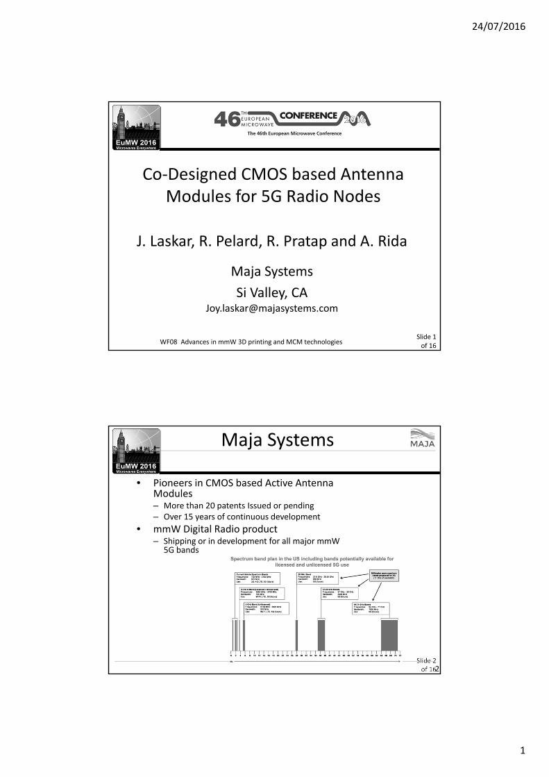
Co‐Designed CMOS based Antenna Modules for 5G Radio Nodes
J. Laskar, R. Pelard, R. Pratap and A. Rida
Maja Systems
Si Valley, [email protected]
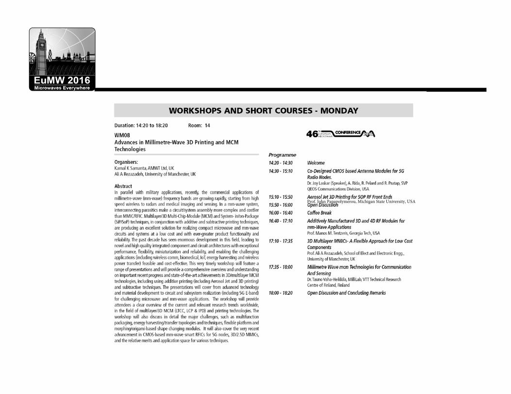
WF08 Advances in mmW 3D printing and MCM technologies
Slide 2of 16
Maja Systems
• Pioneers in CMOS based Active AntennaModules– More than 20 patents Issued or pending– Over 15 years of continuous development
• mmW Digital Radio product– Shipping or in development for all major mmW
5G bands
2
24/07/2016
2
Slide 3of 16
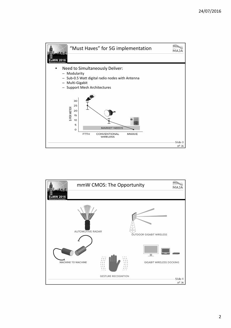
“Must Haves” for 5G implementation
• Need to Simultaneously Deliver:– Modularity– Sub‐0.5 Watt digital radio nodes with Antenna– Multi‐Gigabit– Support Mesh Architectures
Slide 4of 16
mmW CMOS: The Opportunity
24/07/2016
3
Slide 5of 16
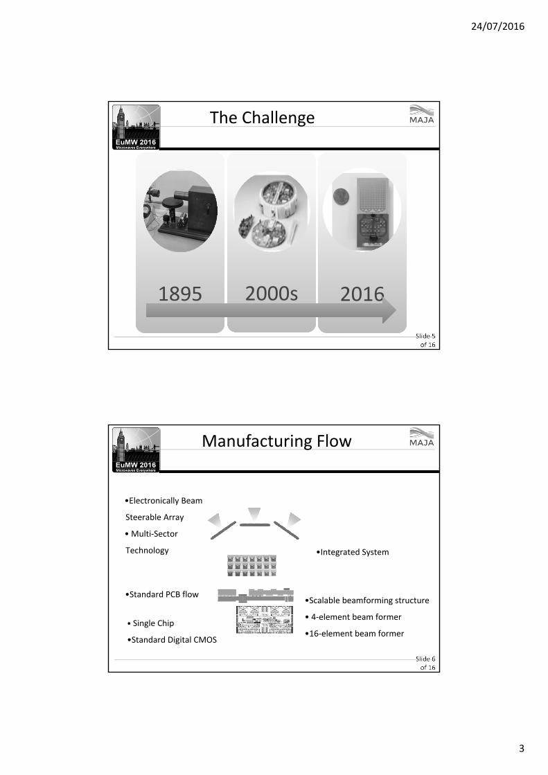
The Challenge
18951895 2000s2000s 20162016
Slide 6of 16
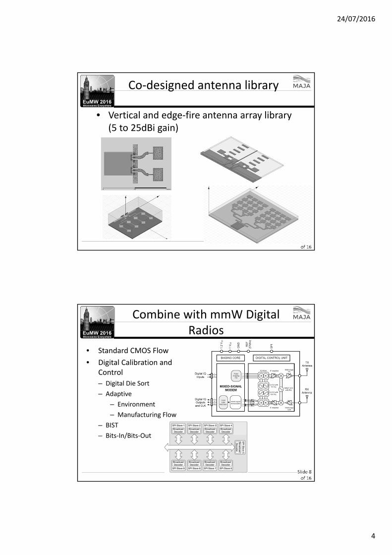
Manufacturing Flow
•Electronically Beam
Steerable Array
• Multi‐Sector
Technology
•Scalable beamforming structure
• 4‐element beam former
•16‐element beam former
•Standard PCB flow
•Integrated System
• Single Chip
•Standard Digital CMOS
24/07/2016
4
Slide 7of 16
Co‐designed antenna library
• Vertical and edge‐fire antenna array library (5 to 25dBi gain)
Slide 8of 16
Combine with mmW Digital Radios
• Standard CMOS Flow
• Digital Calibration and Control
– Digital Die Sort
– Adaptive
– Environment
– Manufacturing Flow
– BIST
– Bits‐In/Bits‐Out
24/07/2016
5
Slide 9of 16
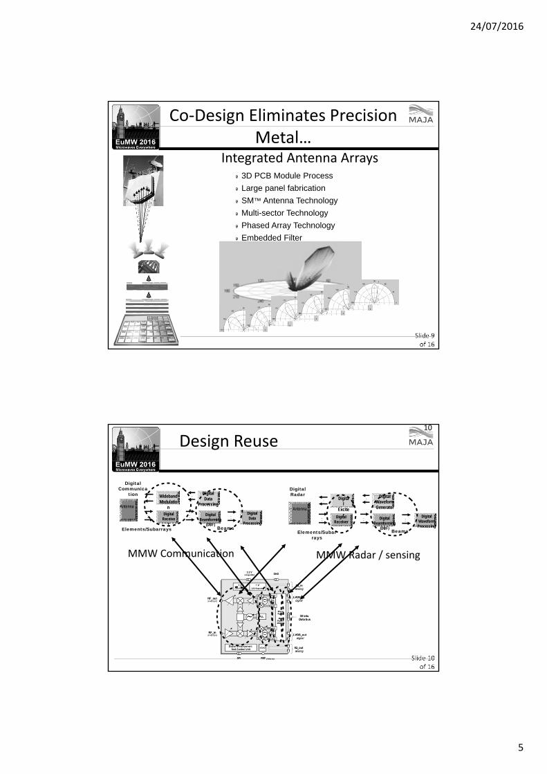
Co‐Design Eliminates Precision Metal…
Integrated Antenna Arrays3D PCB Module Process
Large panel fabrication
SM™ Antenna Technology
Multi-sector Technology
Phased Array Technology
Embedded Filter
Slide 10of 16
Design Reuse10
Antenna
Digital Receiver
Digital
Exciter Digital
WaveformProcessing
••
••
DigitalRadar
Elements/Subarrays
••
••
DigitalWaveformGenerator
Digital Beamforming
(DBF)
••
Beams
Antenna
Digital Receive
r
WidebandModulatio
nDigitalData
Processing
••
••
Elements/Subarrays
••
••
DigitalData
Processing
Digital Beamforming
(DBF)
••
Beams
MMW Radar / sensingMMW Communication
DigitalCommunica
tion
24/07/2016
6
Slide 11of 16
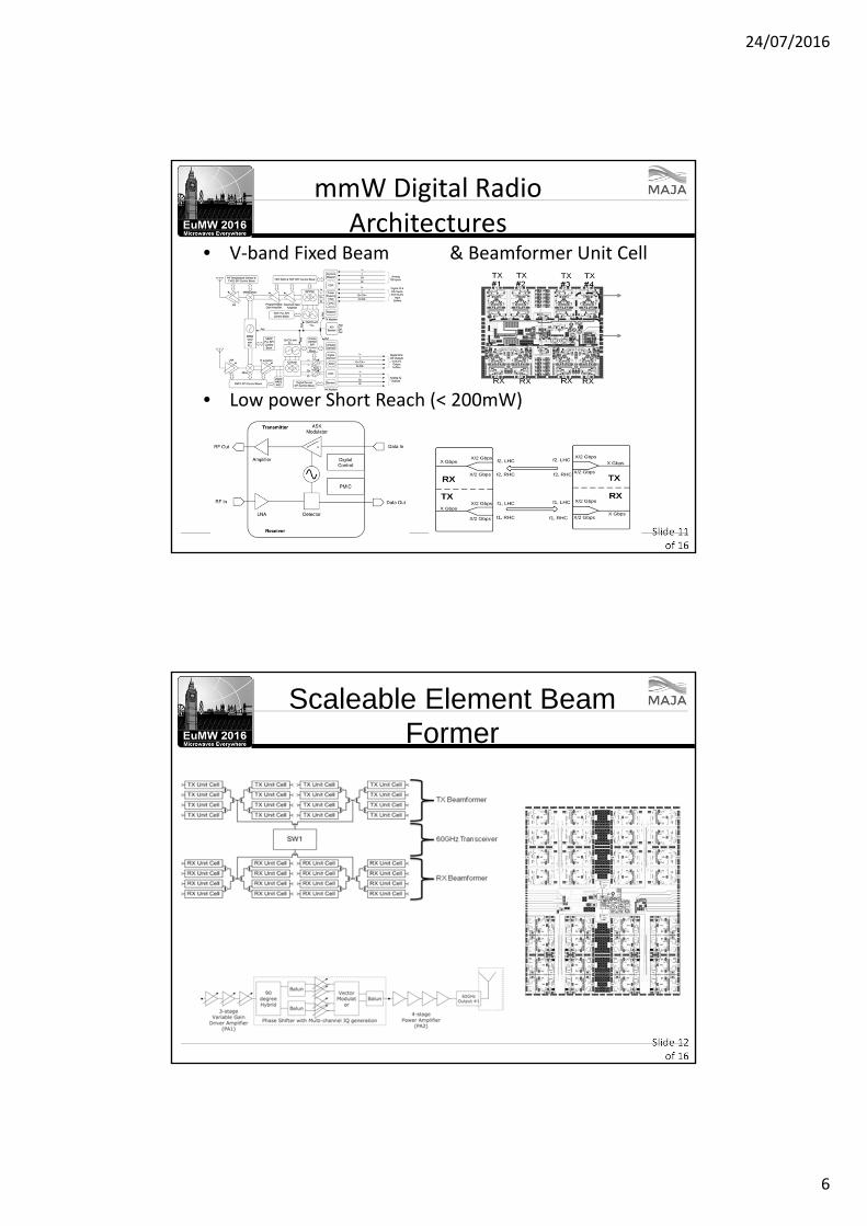
mmW Digital Radio Architectures
• V‐band Fixed Beam & Beamformer Unit Cell
• Low power Short Reach (< 200mW)
Slide 12of 16
Scaleable Element Beam Former
24/07/2016
7
Slide 13of 16
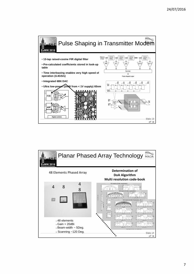
Pulse Shaping in Transmitter Modem
• 13-tap raised-cosine FIR digital filter
• Pre-calculated coefficients stored in look-up table
• Time interleaving enables very high speed of operation (4.4GS/s)
• Integrated 6BIt DAC
• Ultra low-power (2mW from < 1V supply) 65nm
Slide 14of 16
Planar Phased Array Technology
H2 matrix (2 bits resolution)
48 Elements Phased Array Determination of DoA Algorithm
Multi resolution code‐book
4 848
48 elementsGain > 20dBiBeam-width ~ 5Deg.
Scanning ~120 Deg.
H3 matrix (3 bits resolution)
H4 matrix (4 bits resolution, etc..)
24/07/2016
8
Slide 15of 16
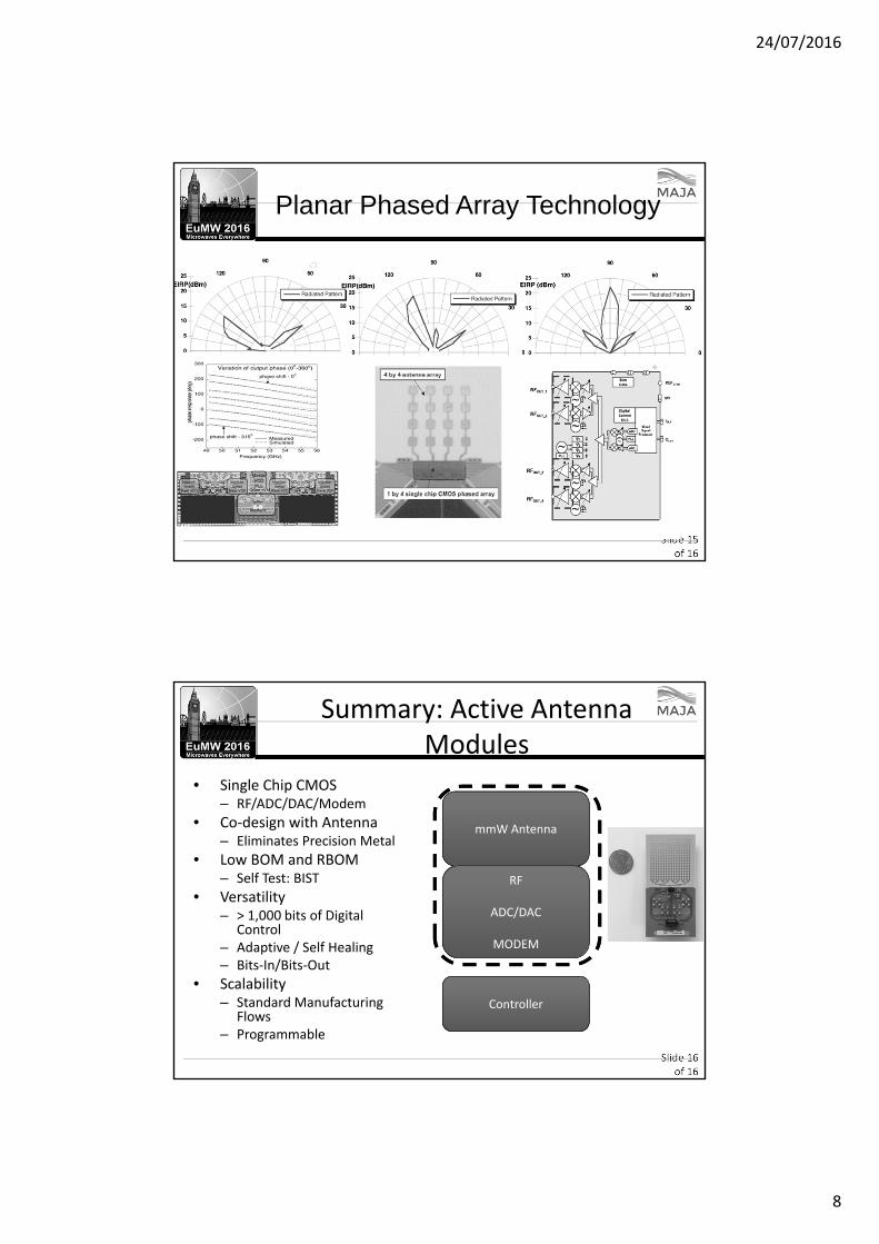
Planar Phased Array Technology
Slide 16of 16
Summary: Active Antenna Modules
• Single Chip CMOS– RF/ADC/DAC/Modem
• Co‐design with Antenna– Eliminates Precision Metal
• Low BOM and RBOM– Self Test: BIST
• Versatility– > 1,000 bits of Digital
Control– Adaptive / Self Healing– Bits‐In/Bits‐Out
• Scalability– Standard Manufacturing
Flows– Programmable
mmW Antenna
RF
ADC/DAC
MODEM
Controller
WM08 Advances in Millimeter-wave 3D Printing and MCM Technologies
Aerosol Jet 3D Printing for SOP RF Front Ends
John PapapolymerouMSU Foundation Professor and Chair
Department of Electrical and Computer EngineeringMichigan State UniversityEast Lansing, MI 48824
2016 European Microwave Conference Workshop WM08 Advances in Millimeter-wave 3D Printing and MCM Technologies
WM08 Advances in Millimeter-wave 3D Printing and MCM Technologies
Outline
• Introduction/Applications• Aerosol Jet Printing Basics• Examples of 3D Manufactured RF and mm-wave circuits• Conclusions
2
3
WM08 Advances in Millimeter-wave 3D Printing and MCM Technologies
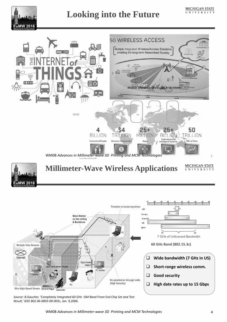
Looking into the Future
Mobile World Congress 2013 - Ericsson
WM08 Advances in Millimeter-wave 3D Printing and MCM Technologies
WM08 Advances in Millimeter-wave 3D Printing and MCM Technologies
Wide bandwidth (7 GHz in US)
Short-range wireless comm.
Good security
High date rates up to 15 Gbps
Millimeter-Wave Wireless Applications
60 GHz Band (802.15.3c)
Source: B.Gaucher, ‘Completely Integrated 60 GHz ISM Band Front End Chip Set and Test Result,’ IEEE 802.06-0003-00-003c, Jan. 9,2006.
4
WM08 Advances in Millimeter-wave 3D Printing and MCM Technologies
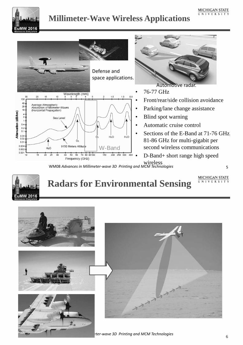
Millimeter-Wave Wireless Applications
5
Defense and space applications.
Automotive radar.• 76-77 GHz• Front/rear/side collision avoidance• Parking/lane change assistance• Blind spot warning• Automatic cruise control• Sections of the E-Band at 71-76 GHz,
81-86 GHz for multi-gigabit per second wireless communications
• D-Band+ short range high speed wireless
W-Band
WM08 Advances in Millimeter-wave 3D Printing and MCM TechnologiesWM08 Advances in Millimeee
Radars for Environmental Sensing
6
WM08 Advances in Millimeter-wave 3D Printing and MCM Technologies
Source: http://www.siemens.com/innovation/en/home/pictures-of-the-future/industry-and-automation/Additive-manufacturing-facts-and-forecasts.html
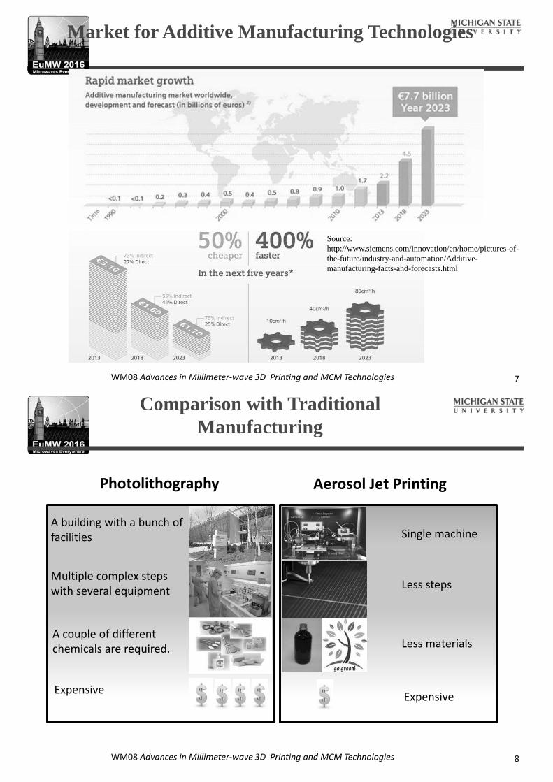
Market for Additive Manufacturing Technologies
7
WM08 Advances in Millimeter-wave 3D Printing and MCM Technologies
Less steps
Polyimide InkSilver Ink
Carrier Gas AerosolVirtual Impactor
Printing Head
A building with a bunch of facilities Single machine
Multiple complex steps with several equipment
A couple of different chemicals are required. Less materials
Photolithography Aerosol Jet Printing
Expensive Expensive
Comparison with Traditional Manufacturing
8
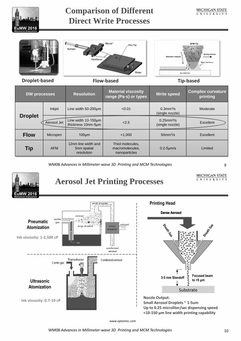
WM08 Advances in Millimeter-wave 3D Printing and MCM Technologies
DW processes ResolutionMaterial viscosity
range (Pa·s) or typesWrite speed
Complex curvature printing
Droplet
Inkjet Line width 50-200μm <0.01 0.3mm3/s(single nozzle)
Moderate
Aerosol JetLine width 10-150μm thickness 10nm-5μm <2.5
0.25mm3/s(single nozzle)
Excellent
Flow Micropen 100μm <1,000 50mm3/s Excellent
Tip AFM12nm line width and
5nm spatial resolution
Thiol molecules, macromolecules,
nanoparticles0.2-5μm/s Limited
Flow-based Tip-basedDroplet-based
Comparison of Different Direct Write Processes
9
WM08 Advances in Millimeter-wave 3D Printing and MCM Technologies
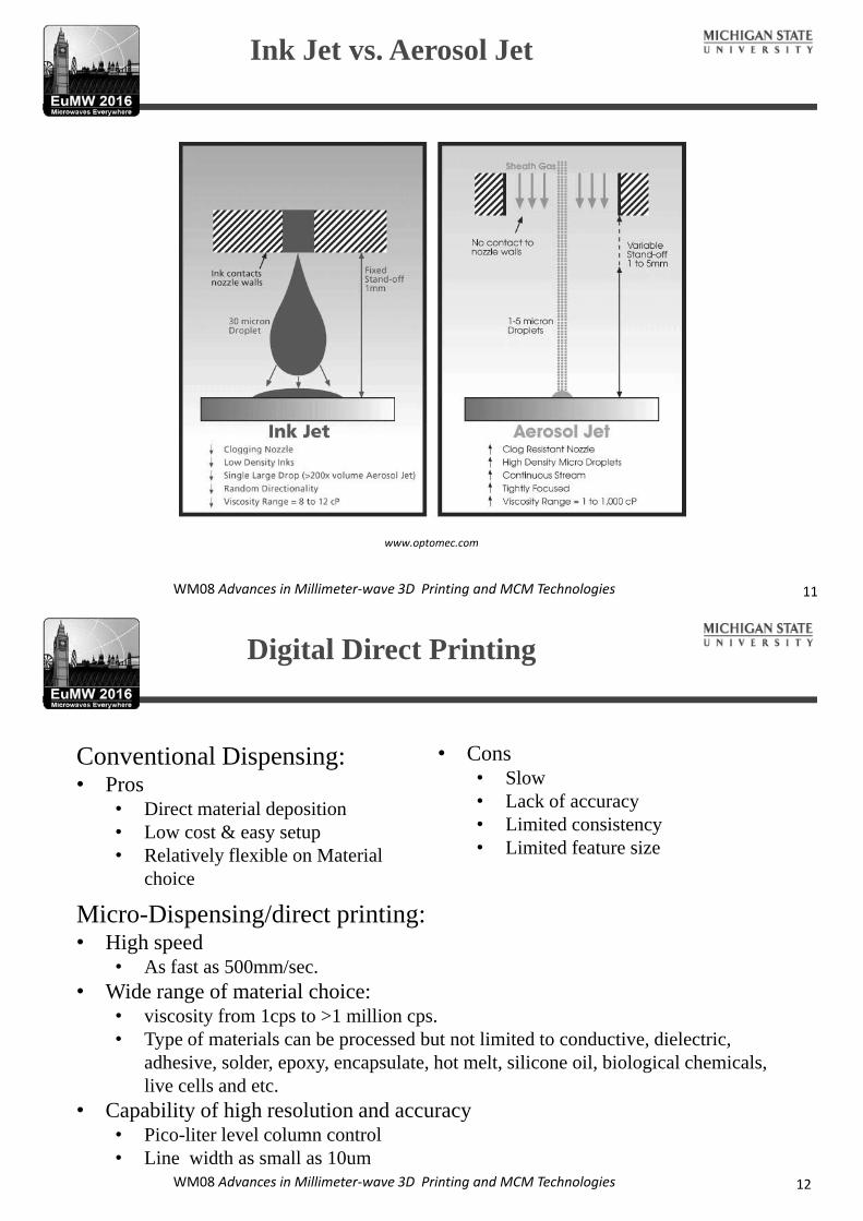
Nozzle Output:Small Aerosol Droplets ~ 1-5umUp to 0.25 microliter/sec dispensing speed<10-150 μm line width printing capability
Ink viscosity: 0.7-10 cP
Sheath Gas In
Focused BeamTo <10um
Dense Aerosol
Substrate
3 to 5mm Standoff
Shea
th G
as In
Sheath Gas In
Focused BeamTo <10um
Dense Aerosol
Substrate
3 to 5mm Standoff
Shea
th G
as In
Printing Head
3-5 mm Standoff Focused beam to <5 μm
Substrate
Gas InGas In
Pneumatic Atomization
UltrasonicAtomization
Ink viscosity: 1-2,500 cP
Condensed aerosolCarrier gas
Transducer
www.optomec.com
Aerosol Jet Printing Processes
10
WM08 Advances in Millimeter-wave 3D Printing and MCM Technologies
www.optomec.com
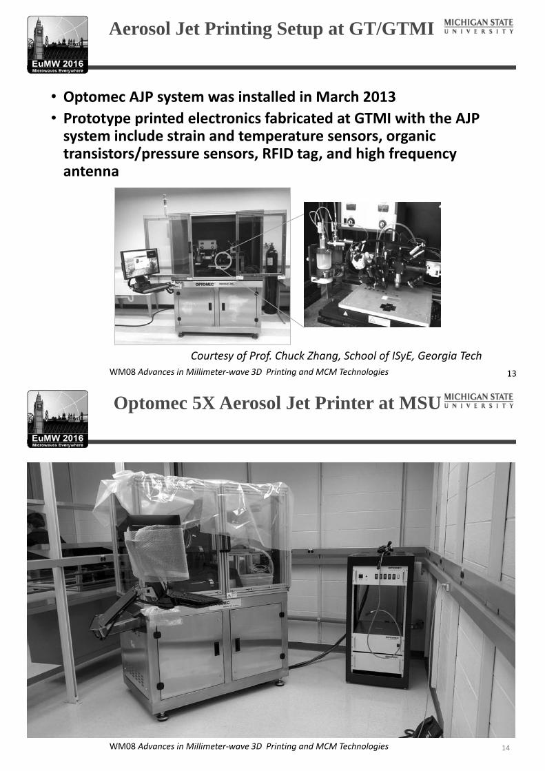
Ink Jet vs. Aerosol Jet
11
WM08 Advances in Millimeter-wave 3D Printing and MCM Technologies
Conventional Dispensing:• Pros
• Direct material deposition• Low cost & easy setup• Relatively flexible on Material
choice
• Cons• Slow• Lack of accuracy• Limited consistency• Limited feature size
Micro-Dispensing/direct printing:• High speed
• As fast as 500mm/sec.• Wide range of material choice:
• viscosity from 1cps to >1 million cps.• Type of materials can be processed but not limited to conductive, dielectric,
adhesive, solder, epoxy, encapsulate, hot melt, silicone oil, biological chemicals, live cells and etc.
• Capability of high resolution and accuracy• Pico-liter level column control• Line width as small as 10um
Digital Direct Printing
12
WM08 Advances in Millimeter-wave 3D Printing and MCM Technologies
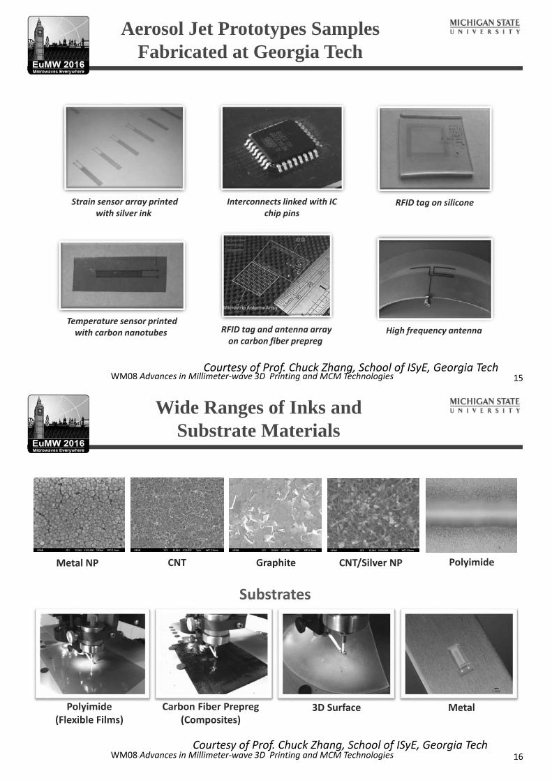
• Optomec AJP system was installed in March 2013• Prototype printed electronics fabricated at GTMI with the AJP
system include strain and temperature sensors, organic transistors/pressure sensors, RFID tag, and high frequency antenna
Courtesy of Prof. Chuck Zhang, School of ISyE, Georgia Tech13
Aerosol Jet Printing Setup at GT/GTMI
WM08 Advances in Millimeter-wave 3D Printing and MCM Technologies 14
Optomec 5X Aerosol Jet Printer at MSU
WM08 Advances in Millimeter-wave 3D Printing and MCM Technologies
Interconnects linked with IC chip pins
RFID tag on silicone
Temperature sensor printedwith carbon nanotubes RFID tag and antenna array
on carbon fiber prepreg
Strain sensor array printedwith silver ink
High frequency antenna
Courtesy of Prof. Chuck Zhang, School of ISyE, Georgia Tech
Aerosol Jet Prototypes Samples Fabricated at Georgia Tech
15
WM08 Advances in Millimeter-wave 3D Printing and MCM Technologies
Graphite CNT/Silver NPMetal NP CNT
Polyimide(Flexible Films)
Carbon Fiber Prepreg(Composites)
3D Surface
Substrates
Metal
Polyimide
Wide Ranges of Inks and Substrate Materials
Courtesy of Prof. Chuck Zhang, School of ISyE, Georgia Tech16
WM08 Advances in Millimeter-wave 3D Printing and MCM Technologies
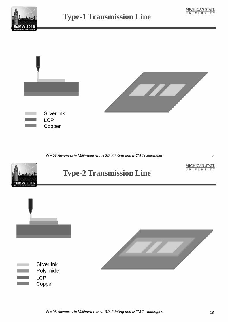
Silver InkLCPCopper
Type-1 Transmission Line
17
WM08 Advances in Millimeter-wave 3D Printing and MCM Technologies
Silver Ink
LCPCopper
Polyimide
Type-2 Transmission Line
18
WM08 Advances in Millimeter-wave 3D Printing and MCM Technologies
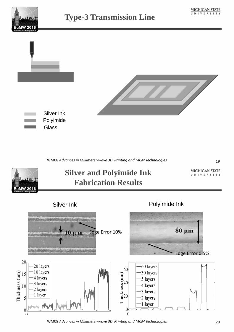
Silver Ink
GlassPolyimide
Type-3 Transmission Line
19
WM08 Advances in Millimeter-wave 3D Printing and MCM Technologies
Silver Ink Polyimide Ink
Edge Error 10%
Edge Error 0.5%
Silver and Polyimide Ink Fabrication Results
20
WM08 Advances in Millimeter-wave 3D Printing and MCM Technologies
Gap= 48 μm
Wsig= 138 μm
L = 2 mm
Wgnd = 1.5 mm
Fabrication Tolerance is 10%.
Silver and Polyimide Ink Fabrication Results
21
WM08 Advances in Millimeter-wave 3D Printing and MCM Technologies
(a) Printed silver ink on 2 mil LCP as type-1(b) the same dimension as type-1 with an additional 10 μm polyimide layer on LCP(c) printed metal-polyimide-metal 3-D structures as type-3 on the glass
Photos of Fabricated Samples
F. Cai, Y.H. Chang, K. Wang, C. Zhan and J. Papapolymerou, “Aerosol Jet Printing for 3D Multilayer Passive Microwave Circuitry,” 2014 IEEE European Microwave Conference, pp. 512-515, Rome, Italy, October 2014
22
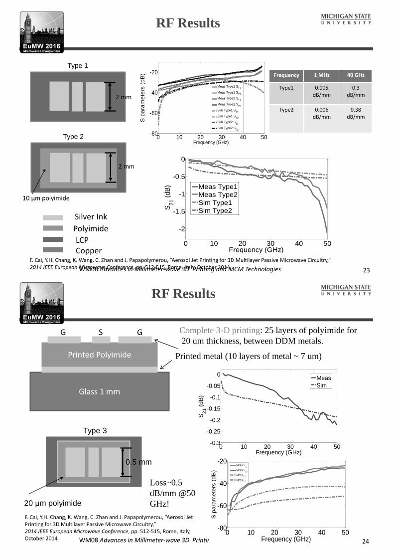
WM08 Advances in Millimeter-wave 3D Printing and MCM Technologies
Silver Ink
LCPCopper
Polyimide
Type 1
Type 2
0 10 20 30 40 50
-2
-1.5
-1
-0.5
0
Frequency (GHz)
S21
(dB
)
Meas Type1Meas Type2Sim Type1Sim Type2
0 10 20 30 40 50-80
-60
-40
-20
Frequency (GHz)S
para
mete
rs (
dB
)
Meas Type1 S11
Meas Type1 S22
Meas Type2 S11
Meas Type2 S22
Sim Type1 S11
Sim Type1 S22
Sim Type2 S11
Sim Type2 S22
2 mm
2 mm
10 μm polyimide
Frequency 1 MHz 40 GHz
Type1 0.005 dB/mm
0.3dB/mm
Type2 0.006 dB/mm
0.38dB/mm
RF Results
F. Cai, Y.H. Chang, K. Wang, C. Zhan and J. Papapolymerou, “Aerosol Jet Printing for 3D Multilayer Passive Microwave Circuitry,” 2014 IEEE European Microwave Conference, pp. 512-515, Rome, Italy, October 2014 23
WM08 Advances in Millimeter-wave 3D Printing and MCM Technologies
0.5 mm
20 μm polyimide
Complete 3-D printing: 25 layers of polyimide for20 um thickness, between DDM metals.
Printed metal (10 layers of metal ~ 7 um)
Type 3
Glass 1 mm
Printed Polyimide
G S G
Loss~0.5 dB/mm @50 GHz!
RF Results
0 10 20 30 40 50-0.3
-0.25
-0.2
-0.15
-0.1
-0.05
0
Frequency (GHz)
S2
1 (
dB)
MeasSim
0 10 20 30 40 50-80
-60
-40
-20
Frequency (GHz)
S p
ara
mete
rs (
dB
)
Meas S11
Meas S22
Sim S11
Sim S11
F. Cai, Y.H. Chang, K. Wang, C. Zhan and J. Papapolymerou, “Aerosol Jet Printing for 3D Multilayer Passive Microwave Circuitry,” 2014 IEEE European Microwave Conference, pp. 512-515, Rome, Italy, October 2014 24
WM08 Advances in Millimeter-wave 3D Printing and MCM Technologies
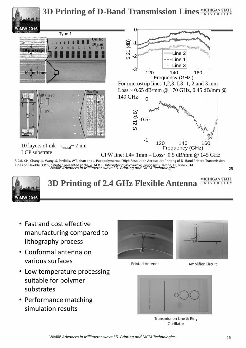
3D Printing of D-Band Transmission Lines
10 m Gap
10 m Line
21 3 4 5 6 7 8 9 10
Units:10 μm
120 140 160-3
-2
-1
0
Frequency (GHz )
S 2
1 (d
B)
Line 2Line 1Line 3
120 140 160-1
-0.5
0
Frequency (GHz)
S 2
1 (d
B)
10 layers of ink – tmetal~ 7 umLCP substrate
For microstrip lines 1,2,3: L3=1, 2 and 3 mmLoss ~ 0.65 dB/mm @ 170 GHz, 0.45 dB/mm @ 140 GHz
CPW line: L4= 1mm – Loss~ 0.5 dB/mm @ 145 GHz
25
Type 1
F. Cai, Y.H. Chang, K. Wang, S. Pavlidis, W.T. Khan and J. Papapolymerou, “High Resolution Aerosol Jet Printing of D- Band Printed TransmissionLines on Flexible LCP Substrate,” presented at the 2014 IEEE International Microwave Symposium, Tampa, FL, June 2014
WM08 Advances in Millimeter-wave 3D Printing and MCM Technologies
• Fast and cost effective manufacturing compared to lithography process
• Conformal antenna on various surfaces
• Low temperature processing suitable for polymer substrates
• Performance matching simulation results
Transmission Line & Ring Oscillator
Amplifier CircuitPrinted Antenna
3D Printing of 2.4 GHz Flexible Antenna
26
WM08 Advances in Millimeter-wave 3D Printing and MCM Technologies
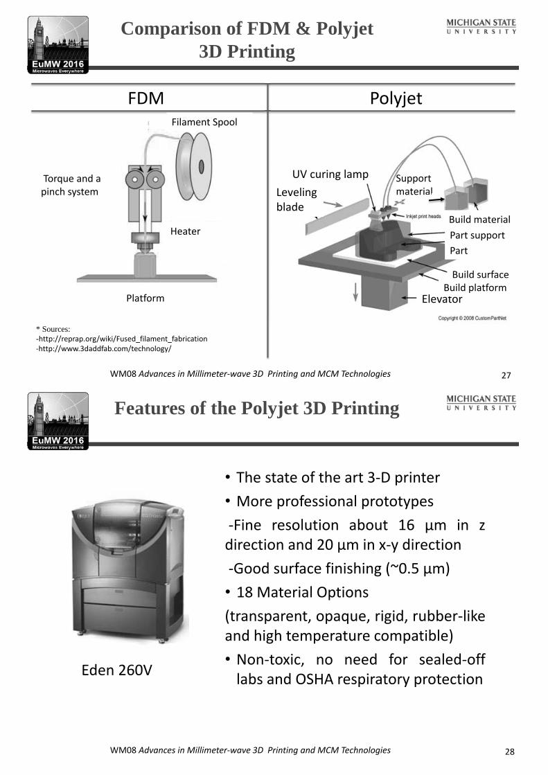
FDM Polyjet
* Sources: -http://reprap.org/wiki/Fused_filament_fabrication-http://www.3daddfab.com/technology/
Filament SpoolFilament is led to the extruder
Heater
UV curing lampLeveling blade
Elevator
Build surfaceBuild platform
Part supportPart
Build material
Support materialal
Torque and a pinch system
Platform
Comparison of FDM & Polyjet3D Printing
27
WM08 Advances in Millimeter-wave 3D Printing and MCM Technologies
• The state of the art 3-D printer• More professional prototypes-Fine resolution about 16 μm in zdirection and 20 μm in x-y direction-Good surface finishing (~0.5 μm)• 18 Material Options(transparent, opaque, rigid, rubber-likeand high temperature compatible)• Non-toxic, no need for sealed-off
labs and OSHA respiratory protectionEden 260V
Features of the Polyjet 3D Printing
28
WM08 Advances in Millimeter-wave 3D Printing and MCM Technologies
ab
d
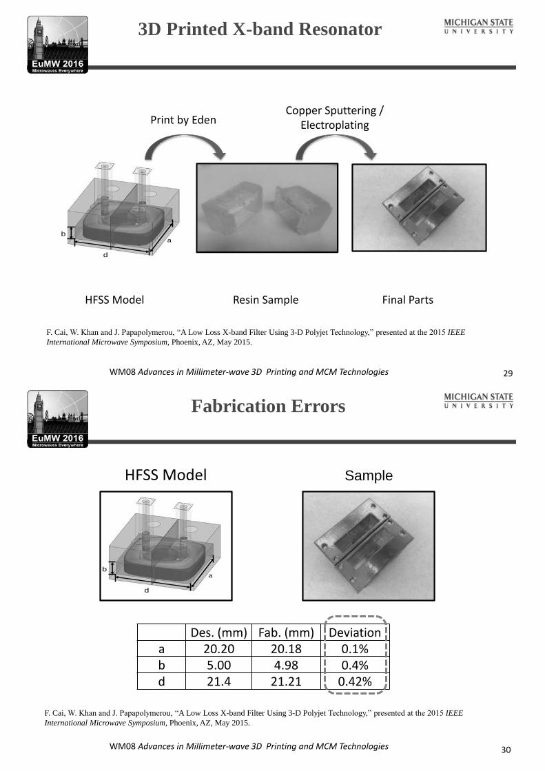
HFSS Model Resin Sample Final Parts
Print by EdenCopper Sputtering /
Electroplating
3D Printed X-band Resonator
F. Cai, W. Khan and J. Papapolymerou, “A Low Loss X-band Filter Using 3-D Polyjet Technology,” presented at the 2015 IEEE International Microwave Symposium, Phoenix, AZ, May 2015.
29
WM08 Advances in Millimeter-wave 3D Printing and MCM Technologies
HFSS Model Sample
Des. (mm) Fab. (mm) Deviationa 20.20 20.18 0.1%b 5.00 4.98 0.4%d 21.4 21.21 0.42%
ab
d
Fabrication Errors
F. Cai, W. Khan and J. Papapolymerou, “A Low Loss X-band Filter Using 3-D Polyjet Technology,” presented at the 2015 IEEE International Microwave Symposium, Phoenix, AZ, May 2015.
30
WM08 Advances in Millimeter-wave 3D Printing and MCM Technologies
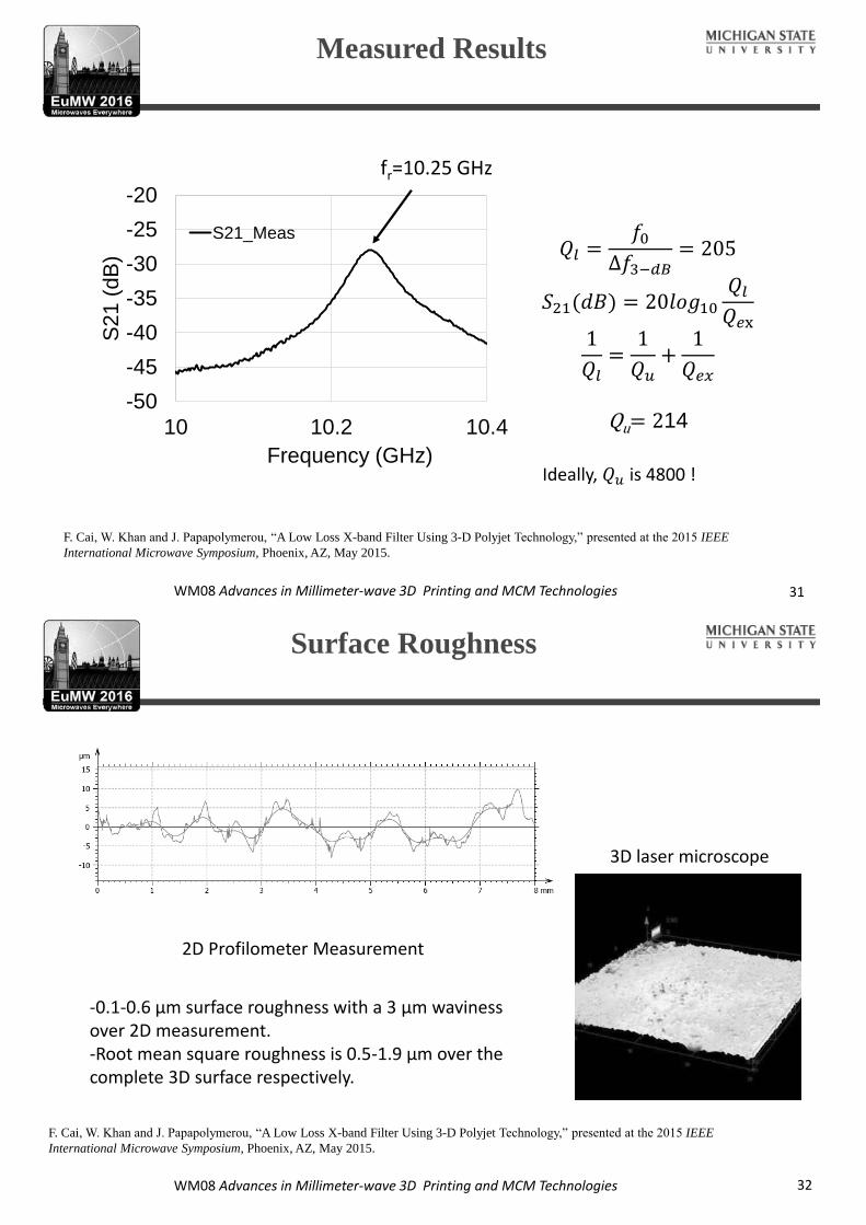
-50
-45
-40
-35
-30
-25
-20
10 10.2 10.4
S21
(dB
)
Frequency (GHz)
S21_Meas
14
fr=10.25 GHz
Ideally, is 4800 !
Measured Results
F. Cai, W. Khan and J. Papapolymerou, “A Low Loss X-band Filter Using 3-D Polyjet Technology,” presented at the 2015 IEEE International Microwave Symposium, Phoenix, AZ, May 2015.
31
WM08 Advances in Millimeter-wave 3D Printing and MCM Technologies
3D laser microscope
2D Profilometer Measurement
-0.1-0.6 μm surface roughness with a 3 μm waviness over 2D measurement. -Root mean square roughness is 0.5-1.9 μm over the complete 3D surface respectively.
Surface Roughness
F. Cai, W. Khan and J. Papapolymerou, “A Low Loss X-band Filter Using 3-D Polyjet Technology,” presented at the 2015 IEEE International Microwave Symposium, Phoenix, AZ, May 2015.
32
WM08 Advances in Millimeter-wave 3D Printing and MCM Technologies
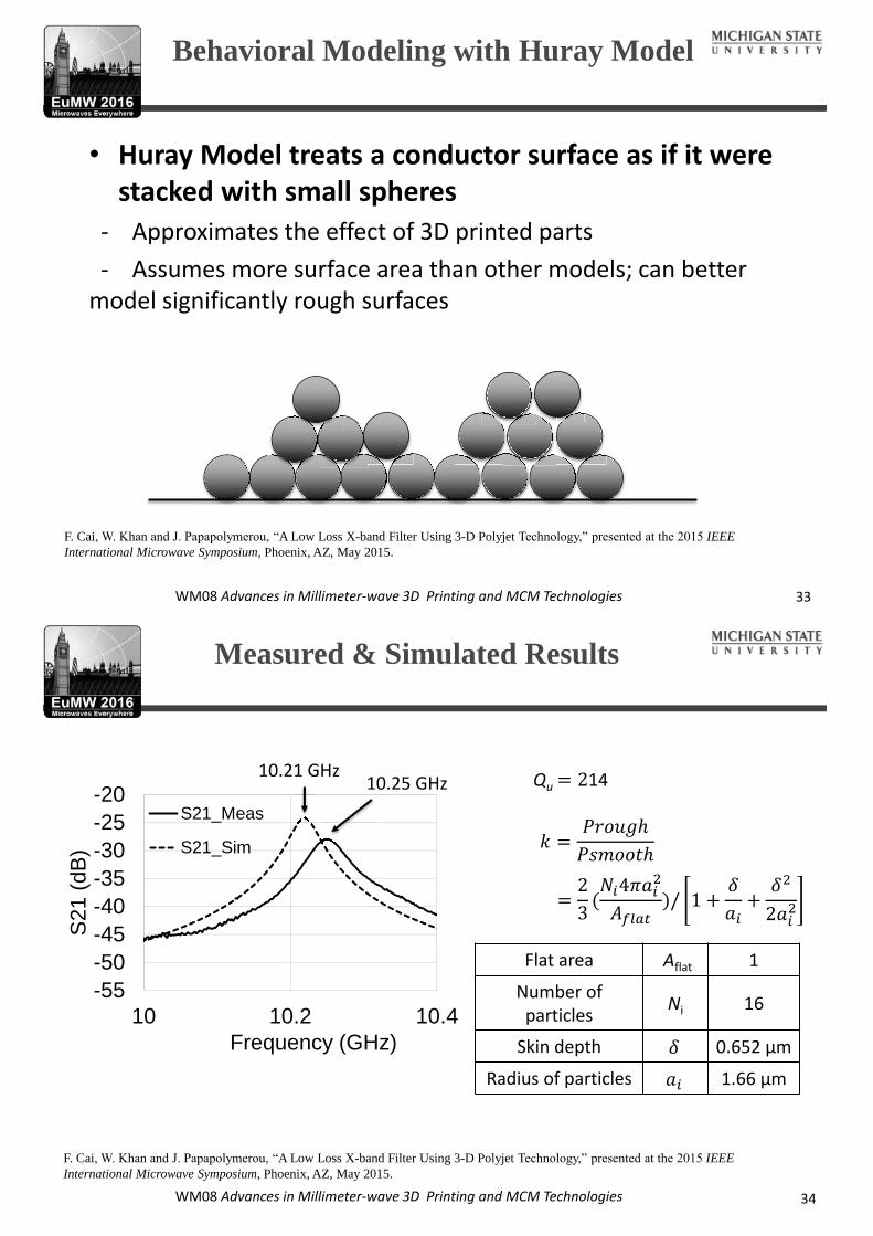
• Huray Model treats a conductor surface as if it were stacked with small spheres
- Approximates the effect of 3D printed parts- Assumes more surface area than other models; can better
model significantly rough surfaces
Behavioral Modeling with Huray Model
F. Cai, W. Khan and J. Papapolymerou, “A Low Loss X-band Filter Using 3-D Polyjet Technology,” presented at the 2015 IEEE International Microwave Symposium, Phoenix, AZ, May 2015.
33
WM08 Advances in Millimeter-wave 3D Printing and MCM Technologies
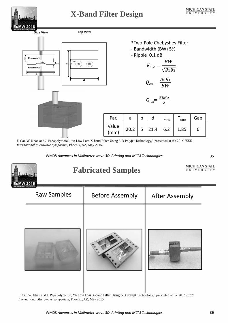
Qu 14
Flat area Aflat 1
Number of particles Ni 16
Skin depth 0.652 μm
Radius of particles 1.66 μm
-55-50-45-40-35-30-25-20
10 10.2 10.4
S21
(dB
)
Frequency (GHz)
S21_Meas
S21_Sim
10.21 GHz10.25 GHz
Measured & Simulated Results
F. Cai, W. Khan and J. Papapolymerou, “A Low Loss X-band Filter Using 3-D Polyjet Technology,” presented at the 2015 IEEE International Microwave Symposium, Phoenix, AZ, May 2015.
34
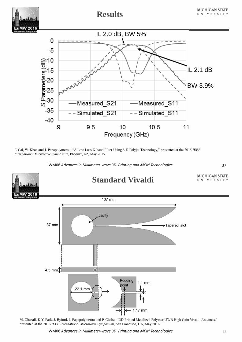
WM08 Advances in Millimeter-wave 3D Printing and MCM Technologies
Resonator1
Resonator 2
b
a
a
d
Gap
Side View Top View
L i r i s Tcont
Q ex
*Two-Pole Chebyshev Filter- Bandwidth (BW) 5% - Ripple 0.1 dB
Par. a b d Liris Tcont Gap
Value (mm) 20.2 5 21.4 6.2 1.85 6
X-Band Filter Design
F. Cai, W. Khan and J. Papapolymerou, “A Low Loss X-band Filter Using 3-D Polyjet Technology,” presented at the 2015 IEEE International Microwave Symposium, Phoenix, AZ, May 2015.
35
WM08 Advances in Millimeter-wave 3D Printing and MCM Technologies
Before Assembly After AssemblyRaw Samples
Fabricated Samples
F. Cai, W. Khan and J. Papapolymerou, “A Low Loss X-band Filter Using 3-D Polyjet Technology,” presented at the 2015 IEEE International Microwave Symposium, Phoenix, AZ, May 2015.
36
WM08 Advances in Millimeter-wave 3D Printing and MCM Technologies
IL 2.1 dB
BW 3.9%
IL 2.0 dB, BW 5%
Results
F. Cai, W. Khan and J. Papapolymerou, “A Low Loss X-band Filter Using 3-D Polyjet Technology,” presented at the 2015 IEEE International Microwave Symposium, Phoenix, AZ, May 2015.
37
38WM08 Advances in Millimeter-wave 3D Printing and MCM Technologies
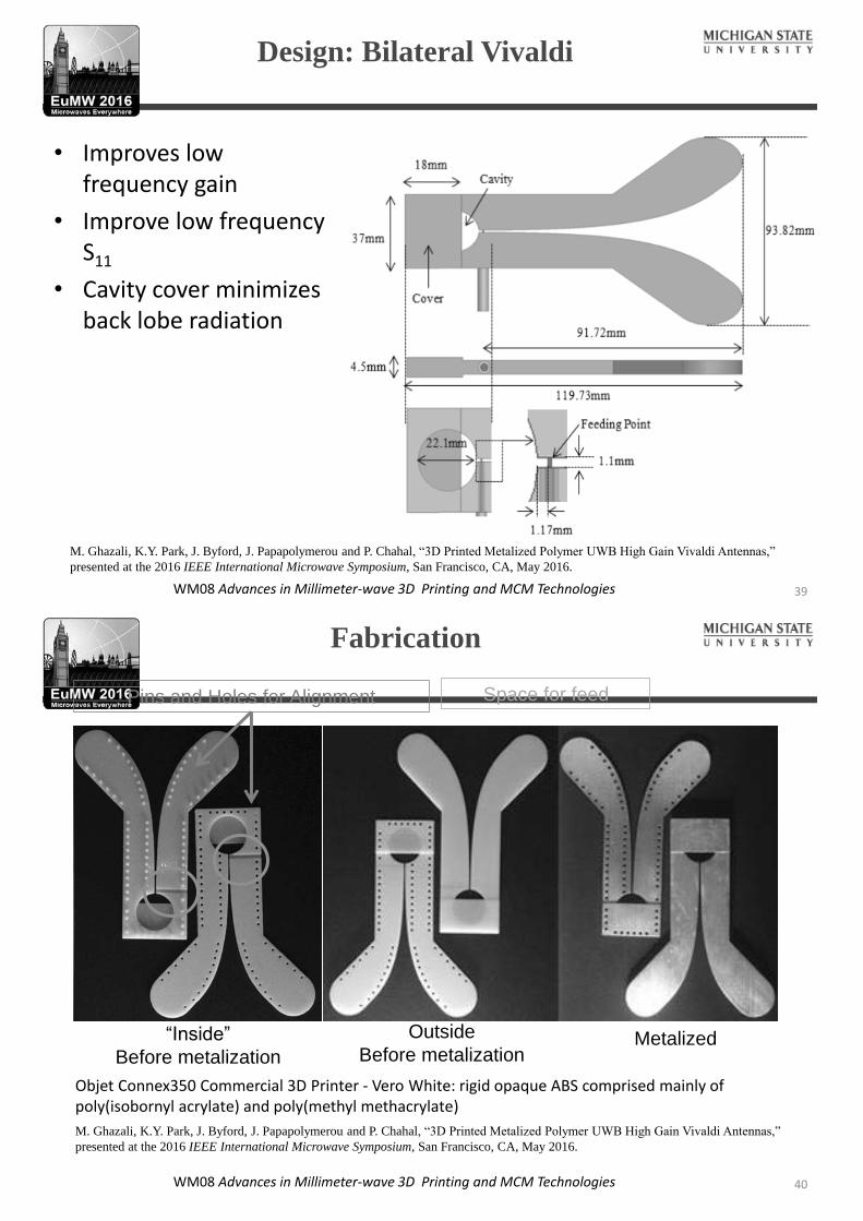
Standard Vivaldi
M. Ghazali, K.Y. Park, J. Byford, J. Papapolymerou and P. Chahal, “3D Printed Metalized Polymer UWB High Gain Vivaldi Antennas,” presented at the 2016 IEEE International Microwave Symposium, San Francisco, CA, May 2016.
39WM08 Advances in Millimeter-wave 3D Printing and MCM Technologies
Design: Bilateral Vivaldi
• Improves low frequency gain
• Improve low frequency S11
• Cavity cover minimizes back lobe radiation
M. Ghazali, K.Y. Park, J. Byford, J. Papapolymerou and P. Chahal, “3D Printed Metalized Polymer UWB High Gain Vivaldi Antennas,” presented at the 2016 IEEE International Microwave Symposium, San Francisco, CA, May 2016.
40WM08 Advances in Millimeter-wave 3D Printing and MCM Technologies
Fabrication
Pins and Holes for Alignment
“Inside” Before metalization
Outside Before metalization
Metalized
Space for feed
M. Ghazali, K.Y. Park, J. Byford, J. Papapolymerou and P. Chahal, “3D Printed Metalized Polymer UWB High Gain Vivaldi Antennas,” presented at the 2016 IEEE International Microwave Symposium, San Francisco, CA, May 2016.
Objet Connex350 Commercial 3D Printer - Vero White: rigid opaque ABS comprised mainly of poly(isobornyl acrylate) and poly(methyl methacrylate)
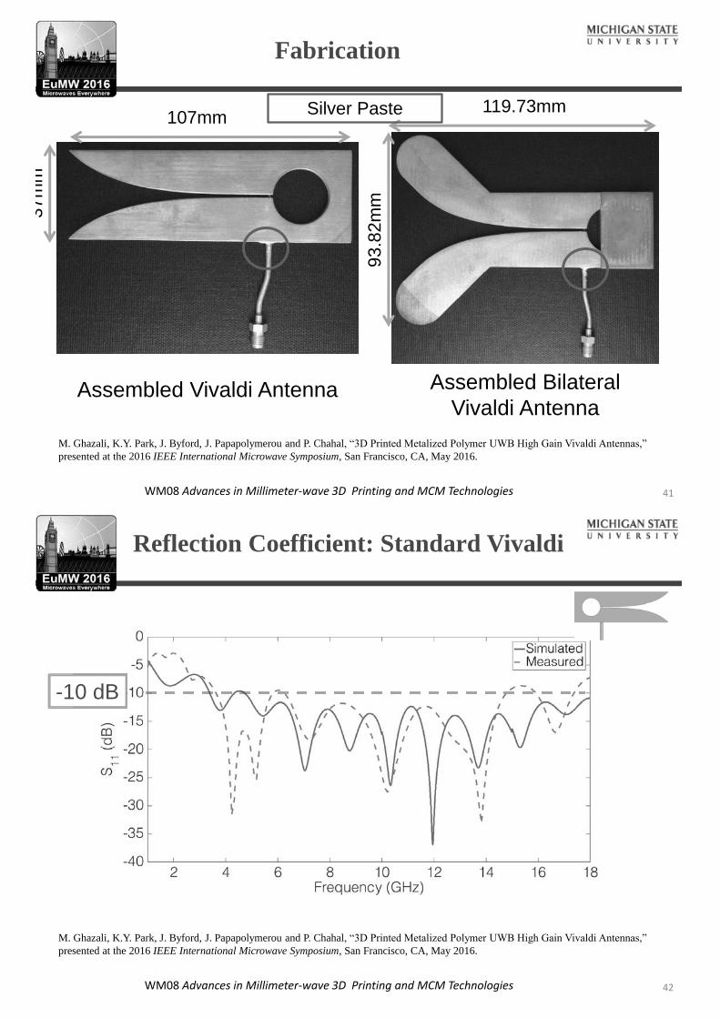
41WM08 Advances in Millimeter-wave 3D Printing and MCM Technologies
Assembled Vivaldi Antenna Assembled Bilateral Vivaldi Antenna
107mm119.73mm
37m
m
93.8
2mm
Silver Paste
Fabrication
M. Ghazali, K.Y. Park, J. Byford, J. Papapolymerou and P. Chahal, “3D Printed Metalized Polymer UWB High Gain Vivaldi Antennas,” presented at the 2016 IEEE International Microwave Symposium, San Francisco, CA, May 2016.
42WM08 Advances in Millimeter-wave 3D Printing and MCM Technologies
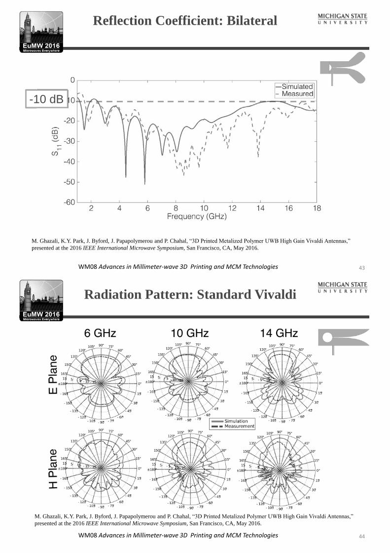
Reflection Coefficient: Standard Vivaldi
-10 dB
M. Ghazali, K.Y. Park, J. Byford, J. Papapolymerou and P. Chahal, “3D Printed Metalized Polymer UWB High Gain Vivaldi Antennas,” presented at the 2016 IEEE International Microwave Symposium, San Francisco, CA, May 2016.
43WM08 Advances in Millimeter-wave 3D Printing and MCM Technologies
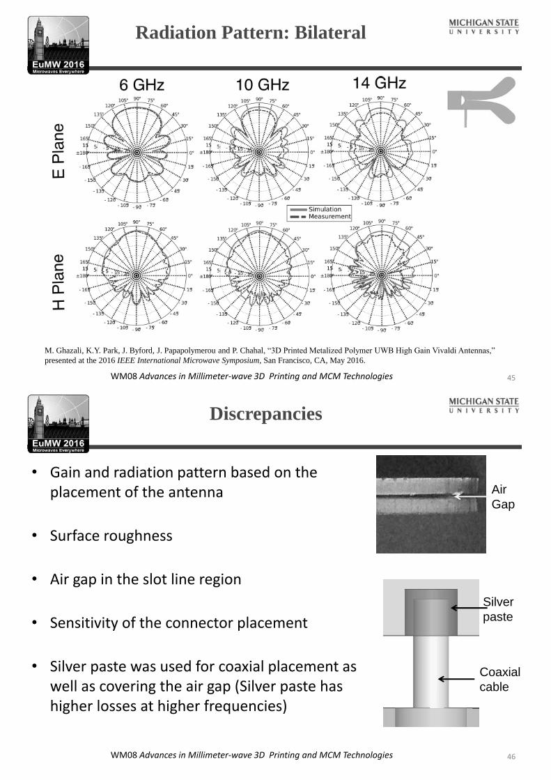
Reflection Coefficient: Bilateral
-10 dB
M. Ghazali, K.Y. Park, J. Byford, J. Papapolymerou and P. Chahal, “3D Printed Metalized Polymer UWB High Gain Vivaldi Antennas,” presented at the 2016 IEEE International Microwave Symposium, San Francisco, CA, May 2016.
44WM08 Advances in Millimeter-wave 3D Printing and MCM Technologies
Radiation Pattern: Standard Vivaldi
M. Ghazali, K.Y. Park, J. Byford, J. Papapolymerou and P. Chahal, “3D Printed Metalized Polymer UWB High Gain Vivaldi Antennas,” presented at the 2016 IEEE International Microwave Symposium, San Francisco, CA, May 2016.
45WM08 Advances in Millimeter-wave 3D Printing and MCM Technologies
Radiation Pattern: Bilateral
M. Ghazali, K.Y. Park, J. Byford, J. Papapolymerou and P. Chahal, “3D Printed Metalized Polymer UWB High Gain Vivaldi Antennas,” presented at the 2016 IEEE International Microwave Symposium, San Francisco, CA, May 2016.
46WM08 Advances in Millimeter-wave 3D Printing and MCM Technologies
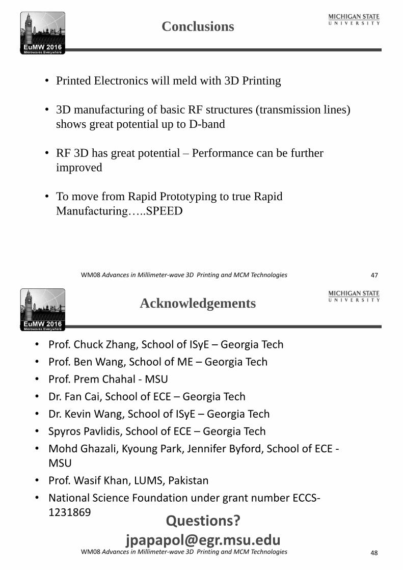
Discrepancies
• Gain and radiation pattern based on the placement of the antenna
• Surface roughness
• Air gap in the slot line region
• Sensitivity of the connector placement
• Silver paste was used for coaxial placement as well as covering the air gap (Silver paste has higher losses at higher frequencies)
Coaxial cable
Silver paste
Air Gap
WM08 Advances in Millimeter-wave 3D Printing and MCM Technologies
Conclusions
• Printed Electronics will meld with 3D Printing
• 3D manufacturing of basic RF structures (transmission lines) shows great potential up to D-band
• RF 3D has great potential – Performance can be further improved
• To move from Rapid Prototyping to true Rapid Manufacturing…..SPEED
47
WM08 Advances in Millimeter-wave 3D Printing and MCM Technologies
Acknowledgements
• Prof. Chuck Zhang, School of ISyE – Georgia Tech• Prof. Ben Wang, School of ME – Georgia Tech• Prof. Prem Chahal - MSU• Dr. Fan Cai, School of ECE – Georgia Tech• Dr. Kevin Wang, School of ISyE – Georgia Tech• Spyros Pavlidis, School of ECE – Georgia Tech• Mohd Ghazali, Kyoung Park, Jennifer Byford, School of ECE -
MSU• Prof. Wasif Khan, LUMS, Pakistan• National Science Foundation under grant number ECCS-
1231869
48
Slide 2 of NNN WF05 Advances in GaN Power Amplifiers: Linearity, Bandwidth and Efficiency
Ali A.Rezazadeh Prof. of Microwave and mm-wave Engineering
University of Manchester, UK [email protected]
3D Multilayer MMICs- A flexible approach for low cost components
Slide 3 of NNN
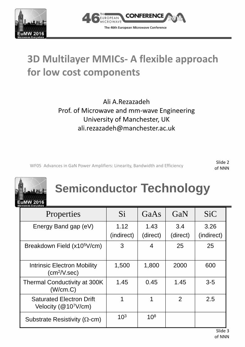
Semiconductor Technology
Properties Si GaAs GaN SiC Energy Band gap (eV) 1.12
(indirect) 1.43
(direct) 3.4
(direct) 3.26
(indirect)
Breakdown Field (x105V/cm)
3 4 25 25
Intrinsic Electron Mobility (cm2/V.sec)
1,500 1,800 2000 600
Thermal Conductivity at 300K (W/cm.C)
1.45 0.45 1.45 3-5
Saturated Electron Drift Velocity (@107V/cm)
1 1 2 2.5
Substrate Resistivity ( -cm) 103 108
Slide 4 of NNN
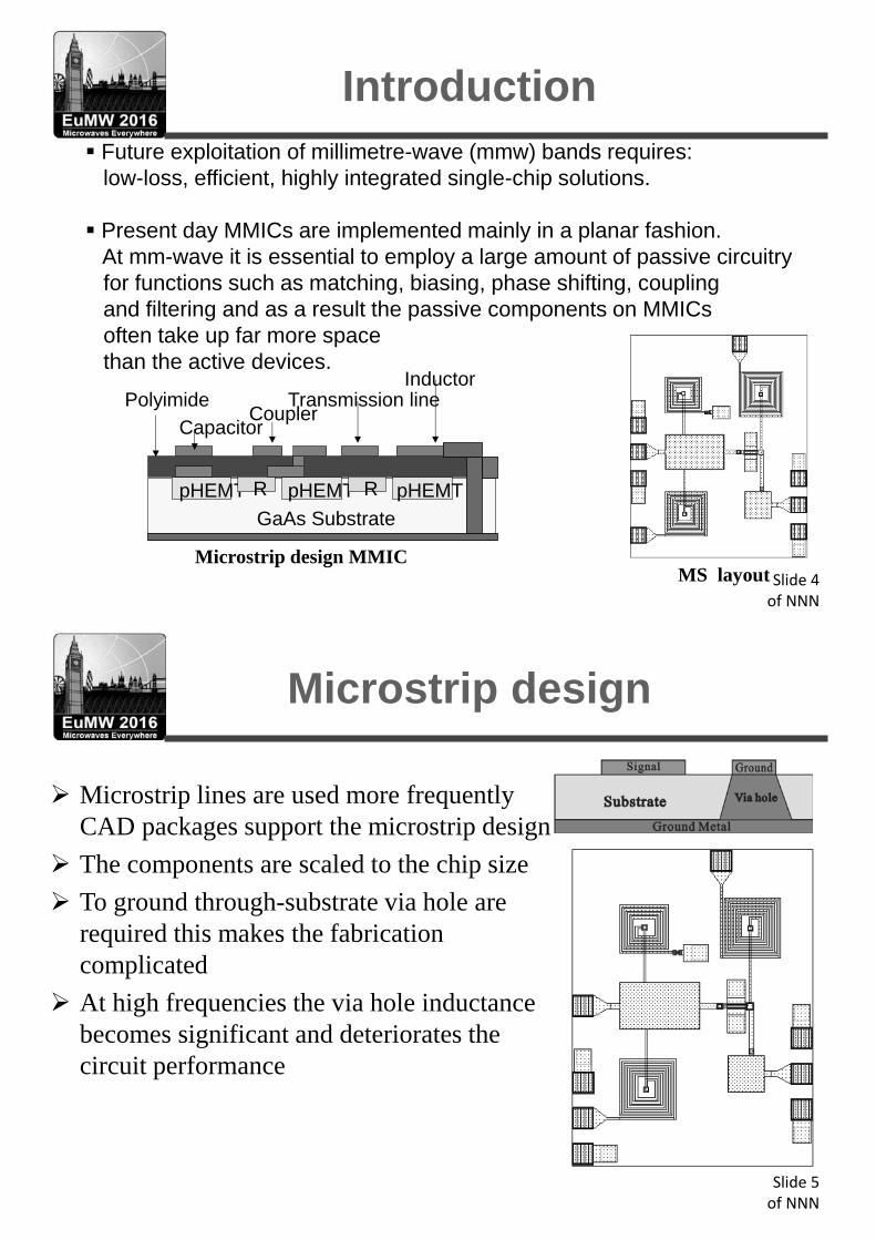
Introduction Future exploitation of millimetre-wave (mmw) bands requires:
low-loss, efficient, highly integrated single-chip solutions. Present day MMICs are implemented mainly in a planar fashion.
At mm-wave it is essential to employ a large amount of passive circuitry for functions such as matching, biasing, phase shifting, coupling and filtering and as a result the passive components on MMICs often take up far more space than the active devices.
pHEMT pHEMT pHEMT R R
Capacitor Coupler
Inductor Polyimide
GaAs Substrate
Transmission line
Microstrip design MMIC MS layout
Slide 5 of NNN
Microstrip design
Microstrip lines are used more frequently CAD packages support the microstrip design The components are scaled to the chip size To ground through-substrate via hole are required this makes the fabrication complicated At high frequencies the via hole inductance becomes significant and deteriorates the circuit performance
Slide 6 of NNN
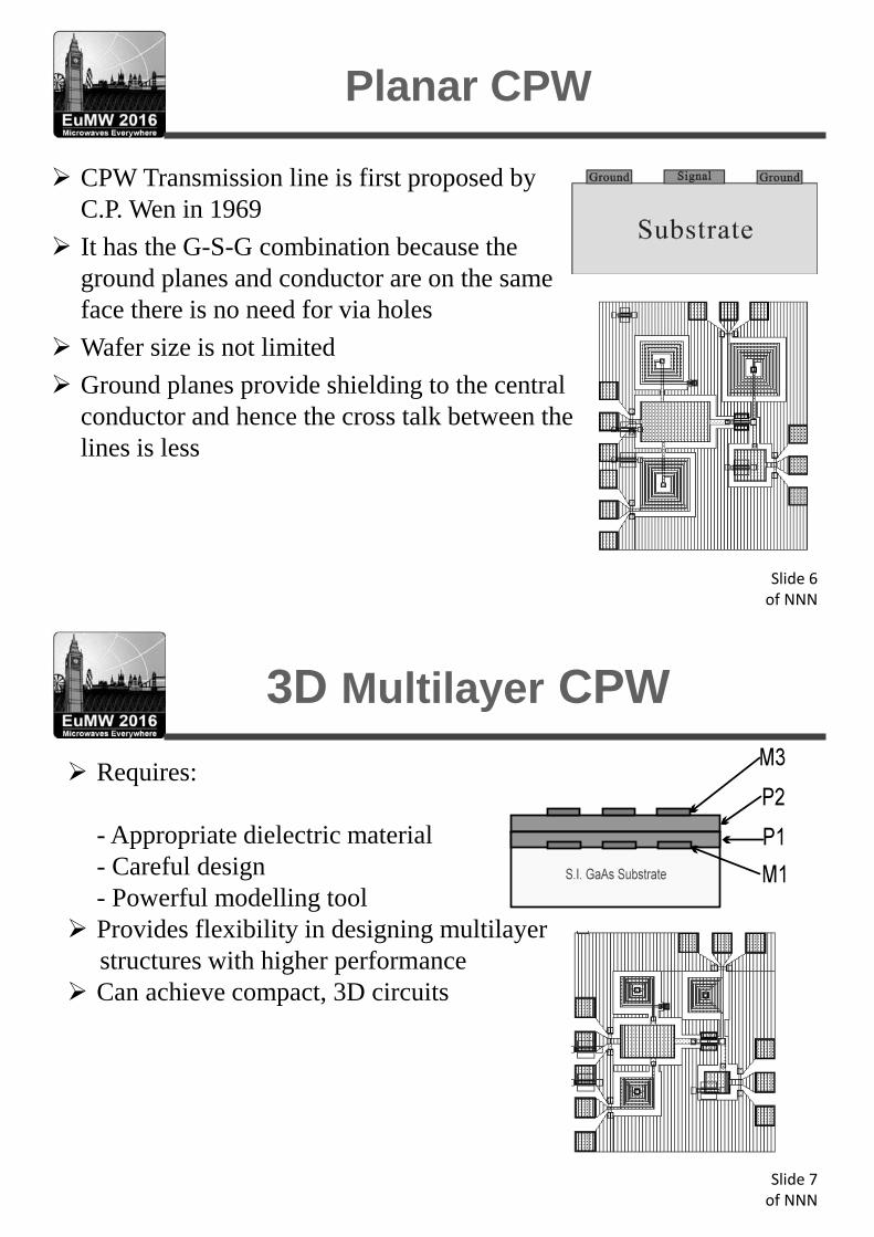
Planar CPW
CPW Transmission line is first proposed by C.P. Wen in 1969 It has the G-S-G combination because the ground planes and conductor are on the same face there is no need for via holes Wafer size is not limited Ground planes provide shielding to the central conductor and hence the cross talk between the lines is less
Slide 7 of NNN
3D Multilayer CPW
Requires: - Appropriate dielectric material - Careful design - Powerful modelling tool
Provides flexibility in designing multilayer structures with higher performance
Can achieve compact, 3D circuits
Slide 8 of NNN
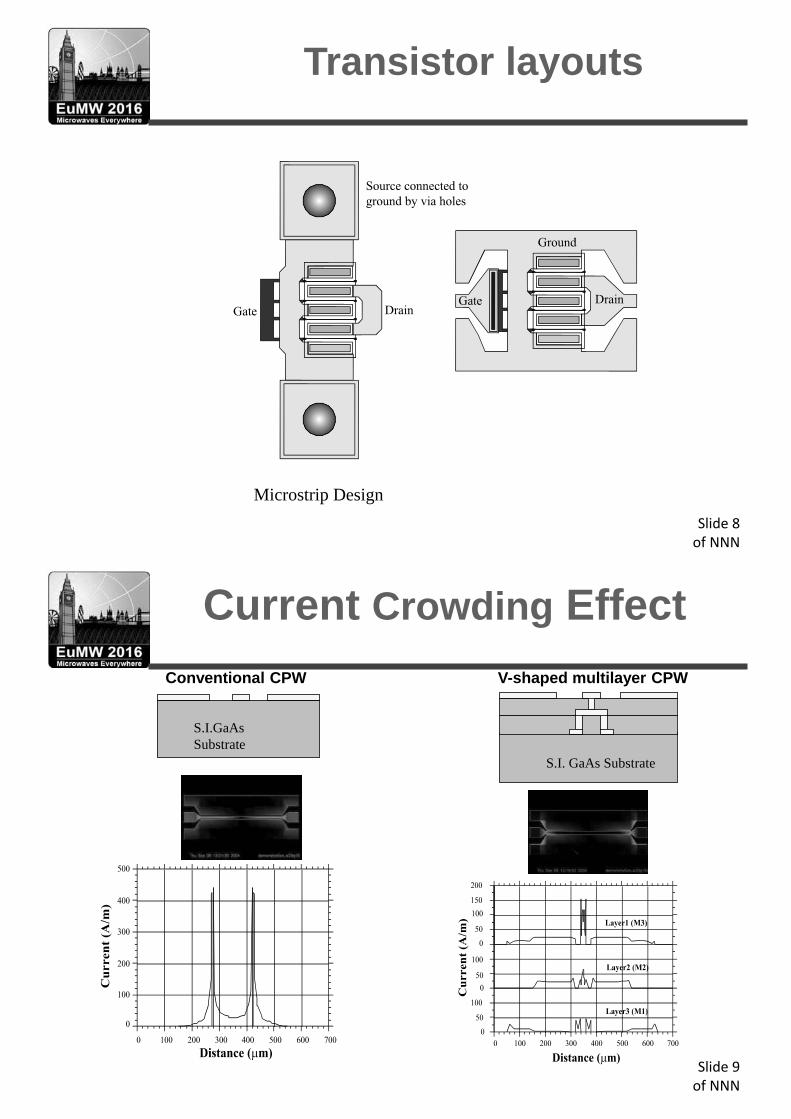
Transistor layouts
Microstrip Design
Slide 9 of NNN
Current Crowding Effect
S.I.GaAs Substrate
S.I. GaAs Substrate
Conventional CPW V-shaped multilayer CPW

Slide 10 of NNN
Transmission Line parameters - 1
CPW parameters:
Characteristic Impedance Z0 Effective Dielectric constant εreff
Dissipation loss The propagation constant is given as
And these parameters can be calculated in different ways, from the measured S-parameters the following relations are used
Slide 11 of NNN
Transmission Line Parameters -2
fc
effectiver 20,
10ln20
10lnln20log20_ leeLossnDissipatio
ll
Where,
C = Velocity of light
l = Length of the transmission line
= Attenuation constant
= Phase constant
Slide 12 of NNN
Transmission Line Parameters- 3
Conductor Loss
- DC Resistance - Surface resistance due to skin effect
f1 1
sR
- current crowding
Dielectric Loss
- Effective Dielectric constant
- Loss tangent
Radiation Loss
Slide 13 of NNN
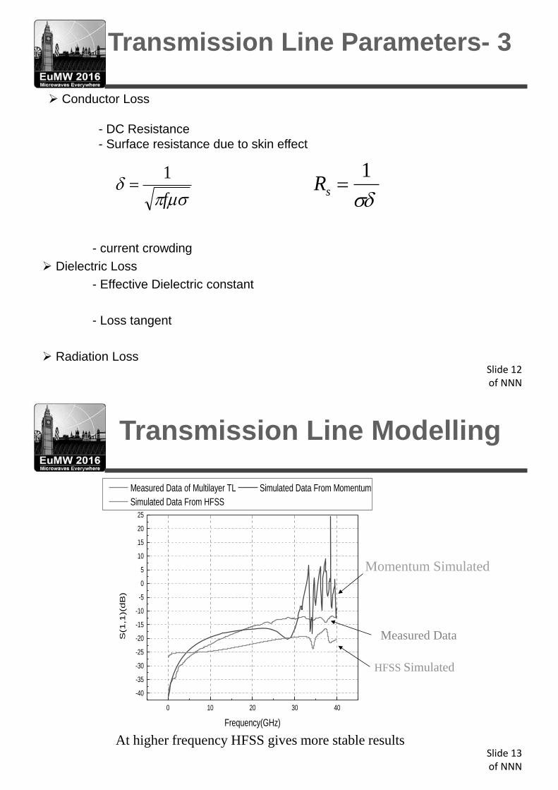
Transmission Line Modelling
0 10 20 30 40
-40
-35
-30
-25
-20
-15
-10
-5
0
5
10
15
20
25
Measured Data of Multilayer TL Simulated Data From Momentum Simulated Data From HFSS
S(1
,1)(
dB
)
Frequency(GHz)
Momentum Simulated
Measured Data
HFSS Simulated
At higher frequency HFSS gives more stable results
Slide 14 of NNN
Effect of Unintentional Horizontal Coupling
Measured coupling between two adjoining transmission lines
S = 75 m (=5G) provides sufficient isolation (30dB) for most application
Van Tuyen Vo, Lokesh Krishnamurthy, Qing Sun, and Ali A. Rezazadeh, “3-D Low-Loss Coplanar Waveguide Transmission Lines in Multilayer MMICs”, IEEE Transactions On Microwave Theory and Techniques, Vol. 54, No. 6, June 2006, pp2864-2871. Doi: 10.1109/TMTT.2006.875458
Slide 15 of NNN
Coupling Effect in MS and CPW Designs
(a) Microstrip coupled lines
(b) CPW coupled lines with ground shield
CPW circuits can be made more compact than MS circuits while good isolation between components can be obtained.
5 10 150 20
-60
-40
-20
-80
0
Frequency (GHz)
S21 [dB
]
MS S=90um
CPW S=90um
MS S=150um
Slide 16 of NNN
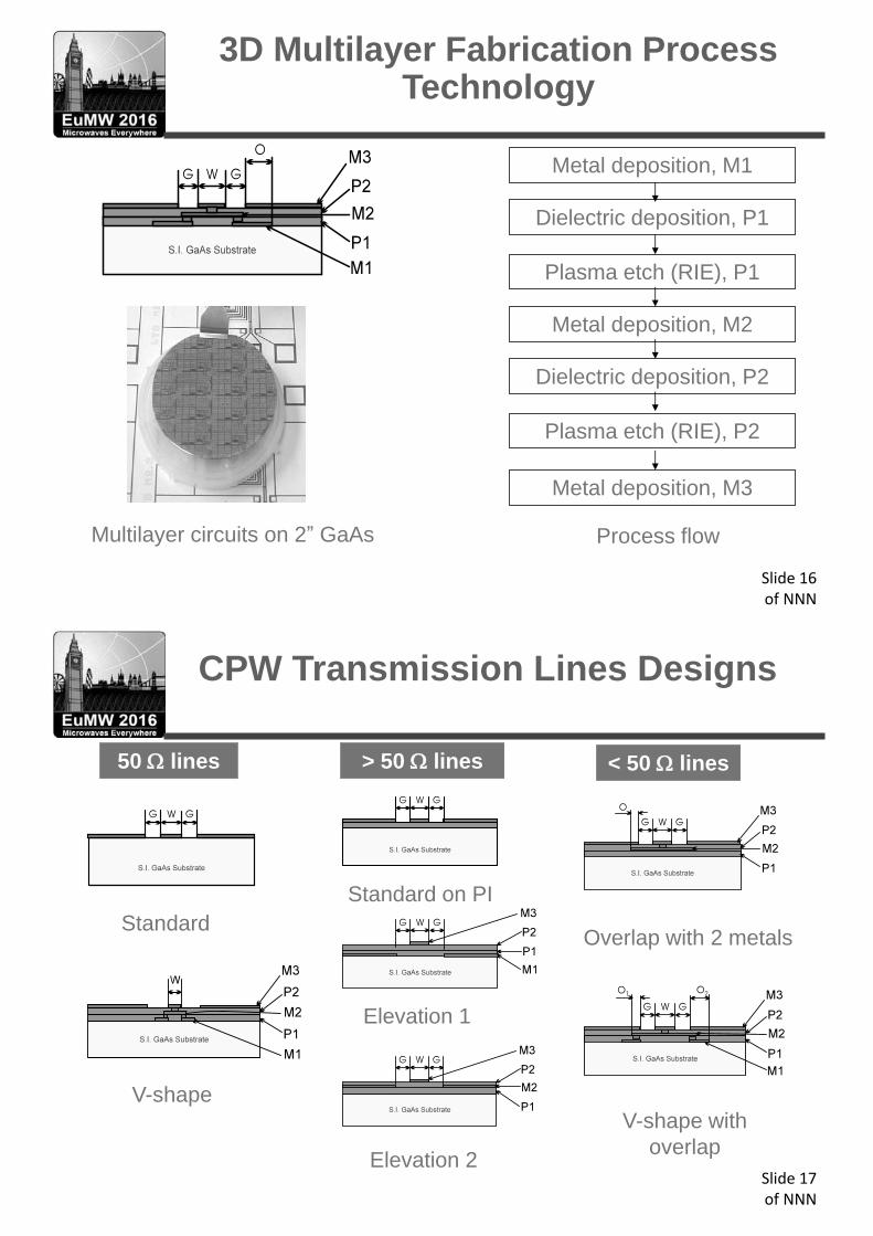
3D Multilayer Fabrication Process Technology
Metal deposition, M1
Dielectric deposition, P1
Plasma etch (RIE), P1
Metal deposition, M2
Dielectric deposition, P2
Plasma etch (RIE), P2
Metal deposition, M3
Process flow Multilayer circuits on 2” GaAs
Slide 17 of NNN
CPW Transmission Lines Designs
50 lines
V-shape
> 50 lines < 50 lines
Overlap with 2 metals
V-shape with overlap
Standard Standard on PI
Elevation 1
Elevation 2
Slide 18 of NNN
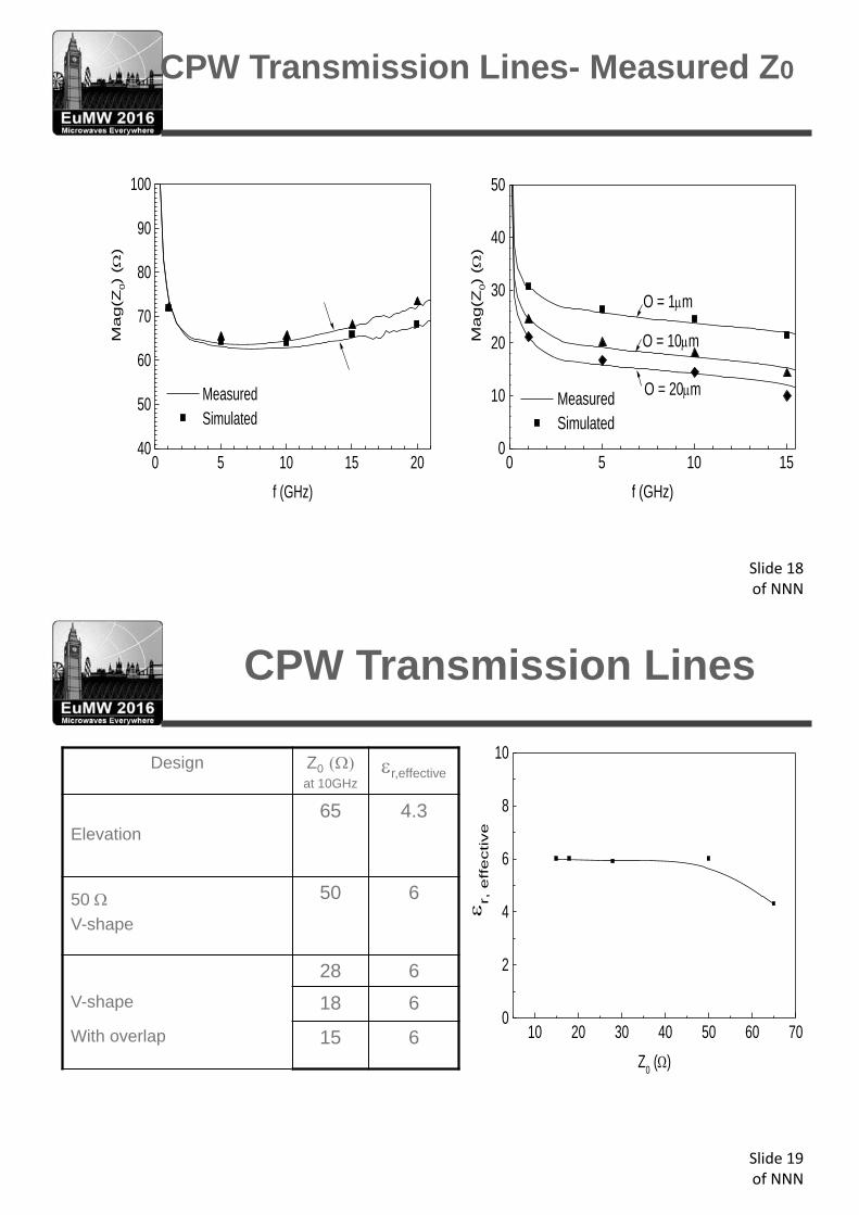
CPW Transmission Lines- Measured Z0
0 5 10 150
10
20
30
40
50
Measured Simulated
O = 20 m
O = 10 m
O = 1 m
Mag(Z
0)
()
f (GHz)
0 5 10 15 2040
50
60
70
80
90
100
Measured Simulated
Mag(Z
0)
()
f (GHz)
Slide 19 of NNN
Design Z0 at 10GHz
r,effective
Elevation 65 4.3
50
V-shape
50 6
28 6
V-shape 18 6
With overlap 15 6 10 20 30 40 50 60 700
2
4
6
8
10
r, e
ffe
ctive
Z0 ( )
CPW Transmission Lines
Slide 20 of NNN
S.I GaAs Substrate
S.I GaAs Substrate
S.I GaAs Substrate
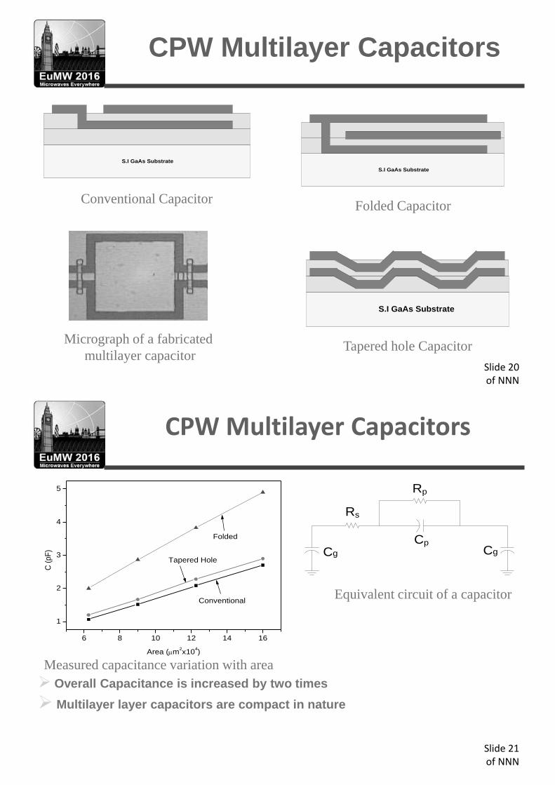
CPW Multilayer Capacitors
Conventional Capacitor Folded Capacitor
Micrograph of a fabricated multilayer capacitor
Tapered hole Capacitor
Slide 21 of NNN
CPW Multilayer Capacitors
6 8 10 12 14 16
1
2
3
4
5
Folded
Tapered Hole
C (p
F)
Area ( m2x104)
Conventional
Overall Capacitance is increased by two times
Multilayer layer capacitors are compact in nature
Measured capacitance variation with area
Equivalent circuit of a capacitor
Rp
Cg
Rs
CpCg
Slide 22 of NNN
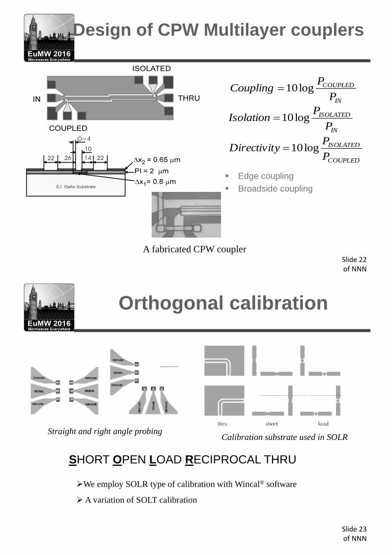
Design of CPW Multilayer couplers
Edge coupling
Broadside coupling
IN
COUPLED
PPCoupling log10
IN
ISOLATED
PPIsolation log10
COUPLED
ISOLATED
PPyDirectivit log10
A fabricated CPW coupler
Slide 23 of NNN
Straight and right angle probing Calibration substrate used in SOLR
We employ SOLR type of calibration with Wincal® software
A variation of SOLT calibration
SHORT OPEN LOAD RECIPROCAL THRU
Orthogonal calibration
Slide 24 of NNN
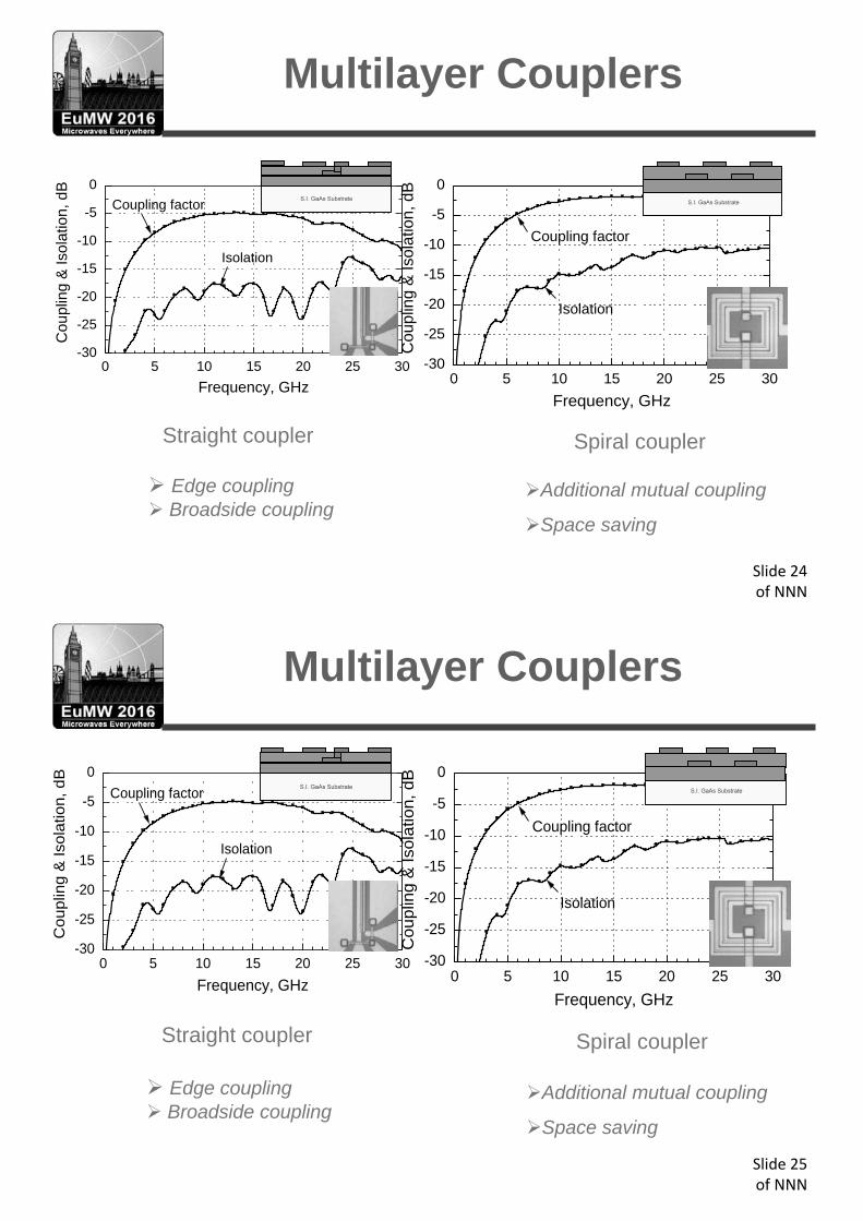
0 5 10 15 20 25 30-30
-25
-20
-15
-10
-5
0
Isolation
Coupling factor
Cou
plin
g &
Isol
atio
n, d
BFrequency, GHz
0 5 10 15 20 25 30-30
-25
-20
-15
-10
-5
0
Isolation
Coupling factor
Cou
plin
g &
Isol
atio
n, d
B
Frequency, GHz
Spiral coupler Straight coupler
Additional mutual coupling
Space saving
Edge coupling Broadside coupling
Multilayer Couplers
Slide 25 of NNN
0 5 10 15 20 25 30-30
-25
-20
-15
-10
-5
0
Isolation
Coupling factor
Co
up
ling
& Iso
latio
n, d
B
Frequency, GHz
0 5 10 15 20 25 30-30
-25
-20
-15
-10
-5
0
Isolation
Coupling factor
Co
up
ling
& Iso
latio
n, d
B
Frequency, GHz
Spiral coupler Straight coupler
Additional mutual coupling
Space saving
Edge coupling Broadside coupling
Multilayer Couplers
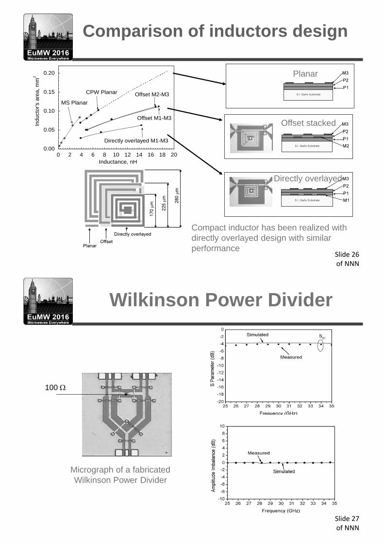
Slide 26 of NNN
Compact inductor has been realized with directly overlayed design with similar performance
0 2 4 6 8 10 12 14 16 18 200.00
0.05
0.10
0.15
0.20
MS Planar
Offset M2-M3
Directly overlayed M1-M3
Offset M1-M3
CPW Planar
Indu
ctor
's a
rea,
mm
2
Inductance, nH
Planar
Offset stacked
Directly overlayed
Comparison of inductors design
Slide 27 of NNN
Micrograph of a fabricated Wilkinson Power Divider
100
Wilkinson Power Divider
Slide 28 of NNN
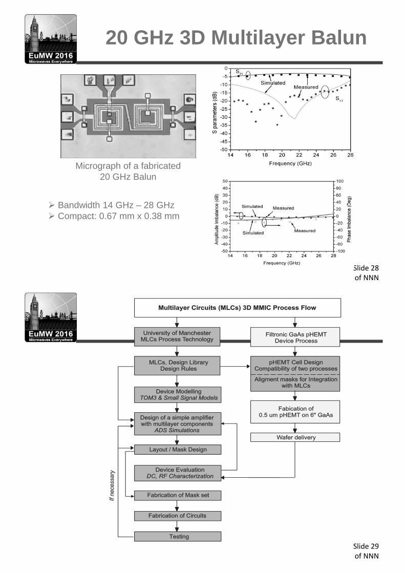
Bandwidth 14 GHz – 28 GHz Compact: 0.67 mm x 0.38 mm
Micrograph of a fabricated 20 GHz Balun
20 GHz 3D Multilayer Balun
Slide 29 of NNN
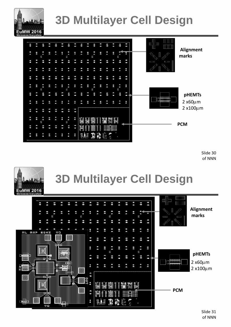
Slide 30 of NNN
Alignment marks
PCM
pHEMTs 2 x60 m 2 x100 m
3D Multilayer Cell Design
Slide 31 of NNN
Alignment marks
PCM
pHEMTs 2 x60 m 2 x100 m
3D Multilayer Cell Design
Slide 32 of NNN
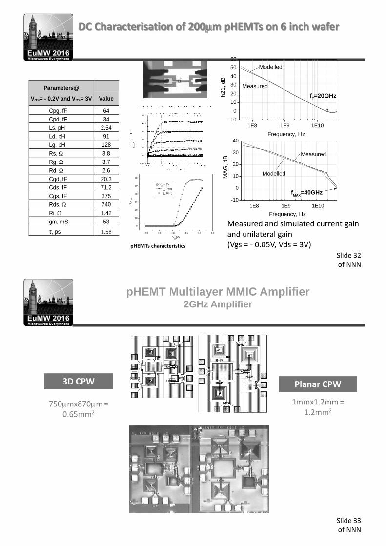
DC Characterisation of 200 m pHEMTs on 6 inch wafer
-2.0 -1.5 -1.0 -0.5 0.0 0.5
0
10
20
30
40
50
60
g m, I
ds
Vgs
(V)
@ Vds
= 3V
Ids
(mA)
gm (mS)
Measured and simulated current gain and unilateral gain (Vgs = - 0.05V, Vds = 3V) pHEMTs characteristics
1E8 1E9 1E10-10
0
10
20
30
40
50
60
fT=20GHz
Modelled
Measured
h21,
dB
Frequency, Hz
1E8 1E9 1E10-10
0
10
20
30
40
fMAX
=40GHz
Modelled
Measured
MA
G, d
B
Frequency, Hz
Parameters@
VGS= - 0.2V and VDS= 3V Value
Cpg, fF 64
Cpd, fF 34
Ls, pH 2.54
Ld, pH 91
Lg, pH 128
Rs, 3.8
Rg, 3.7
Rd, 2.6
Cgd, fF 20.3
Cds, fF 71.2
Cgs, fF 375
Rds, 740
Ri, 1.42
gm, mS 53
, ps 1.58
Slide 33 of NNN
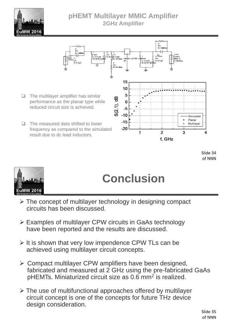
Planar CPW 3D CPW
750 mx870 m = 0.65mm2
1mmx1.2mm = 1.2mm2
pHEMT Multilayer MMIC Amplifier 2GHz Amplifier
Slide 34 of NNN
The multilayer amplifier has similar performance as the planar type while reduced circuit size is achieved.
The measured data shifted to lower frequency as compared to the simulated result due to dc lead inductors.
pHEMT Multilayer MMIC Amplifier 2GHz Amplifier
Slide 35 of NNN
The concept of multilayer technology in designing compact circuits has been discussed.
Examples of multilayer CPW circuits in GaAs technology
have been reported and the results are discussed. It is shown that very low impendence CPW TLs can be
achieved using multilayer circuit concepts.
Compact multilayer CPW amplifiers have been designed, fabricated and measured at 2 GHz using the pre-fabricated GaAs pHEMTs. Miniaturized circuit size as 0.6 mm2 is realized.
The use of multifunctional approaches offered by multilayer
circuit concept is one of the concepts for future THz device design consideration.
Conclusion

Slide 36 of NNN
Acknowledgement
- Peter Kyabaggu - Kila Haris - Dr Emerson Sinulingga - Dr Junyi Yuan - Dr Qing Sun - Dr Tuyn Vo
13/07/2016
1
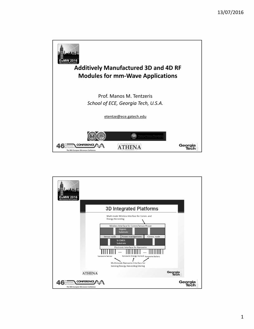
Additively Manufactured 3D and 4D RF Modules for mm‐Wave Applications
Prof. Manos M. Tentzeris
School of ECE, Georgia Tech, U.S.A.
13/07/2016
2
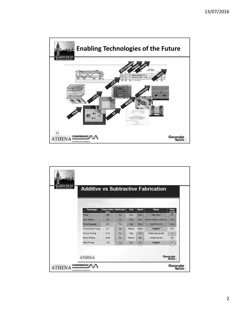
Enabling Technologies of the Future
F2
13/07/2016
3
Internet of Things
13/07/2016
4
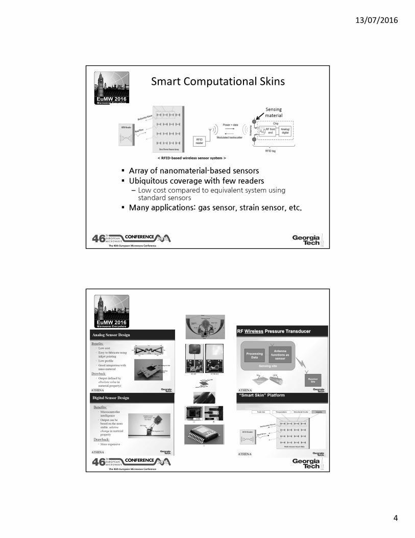
Smart Computational Skins
13/07/2016
5
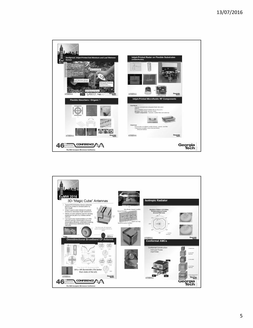
13/07/2016
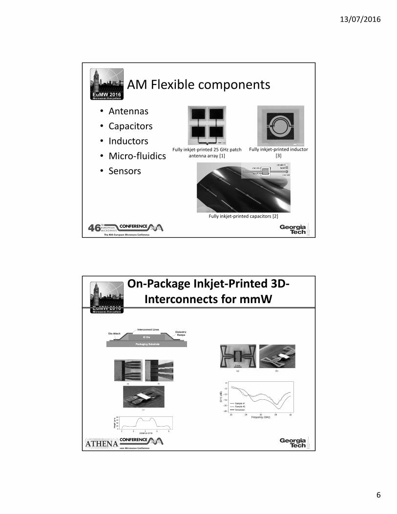
6
• Antennas
• Capacitors
• Inductors
• Micro‐fluidics
• Sensors
AM Flexible components
Fully inkjet‐printed 25 GHz patch antenna array [1]
Fully inkjet‐printed inductor [3]
Fully inkjet‐printed capacitors [2]
On‐Package Inkjet‐Printed 3D‐Interconnects for mmW
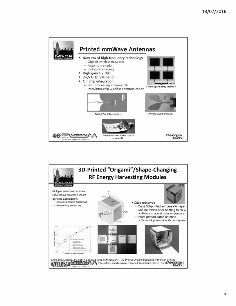
13/07/2016
7
3D‐Printed “Origami”/Shape‐Changing RF Energy Harvesting Modules
J.Kimionis, M.Isakov, B.S.Koh, A.Georgiadis and M.M.Tentzeris, ``3D‐Printed Origami Packaging with Inkjet‐Printed Antennas for RF Harvesting Sensors", IEEE Transactions on Microwave Theory & Techniques, Vol.63, No.12, pp.4521‐4532,December 2015.
13/07/2016
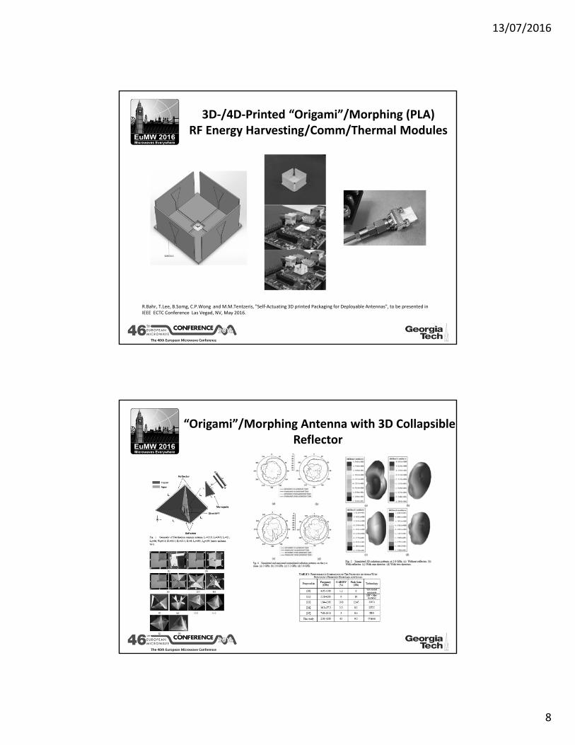
8
3D‐/4D‐Printed “Origami”/Morphing (PLA) RF Energy Harvesting/Comm/Thermal Modules
R.Bahr, T.Lee, B.Somg, C.P.Wong and M.M.Tentzeris, "Self‐Actuating 3D printed Packaging for Deployable Antennas", to be presented in IEEE ECTC Conference Las Vegad, NV, May 2016.
“Origami”/Morphing Antenna with 3D Collapsible Reflector
13/07/2016
9
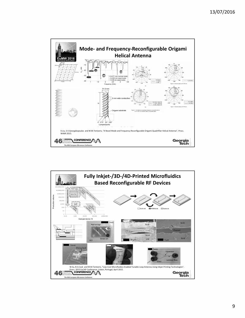
Mode‐ and Frequency‐Reconfigurable Origami Helical Antenna
X.Liu, S.V.Georgakopoulos and M.M.Tentzeris, “A Novel Mode and Frequency Reconfigurable Origami Quadrifilar Helical Antenna”, Procs. WAMI 2015.
Fully Inkjet‐/3D‐/4D‐Printed Microfluidics Based Reconfigurable RF Devices
W.Su, B.S.Cook and M.M.Tentzeris, “Low‐Cost Microfluidics‐Enabled Tunable Loop Antenna Using Inkjet‐Printing Technologies”,Procs. 2015 EuCAP Conference, Lisbon, Portugal, April 2015.
13/07/2016
10
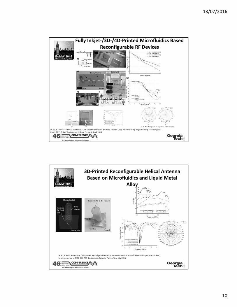
Fully Inkjet‐/3D‐/4D‐Printed Microfluidics Based Reconfigurable RF Devices
W.Su, B.S.Cook and M.M.Tentzeris, “Low‐Cost Microfluidics‐Enabled Tunable Loop Antenna Using Inkjet‐Printing Technologies”,Procs. 2015 EuCAP Conference, Lisbon, Portugal, April 2015.
3D‐Printed Reconfigurable Helical Antenna Based on Microfluidics and Liquid Metal
Alloy
W.Su, R.Bahr, S.Nauroze, “3D printed Reconfigurable Helical Antenna Based on Microfluidics and Liquid Metal Alloy”,to be presented in 2016 IEEE APS Conference, Fajardo, Puerto Rico, July 2016.
13/07/2016
11
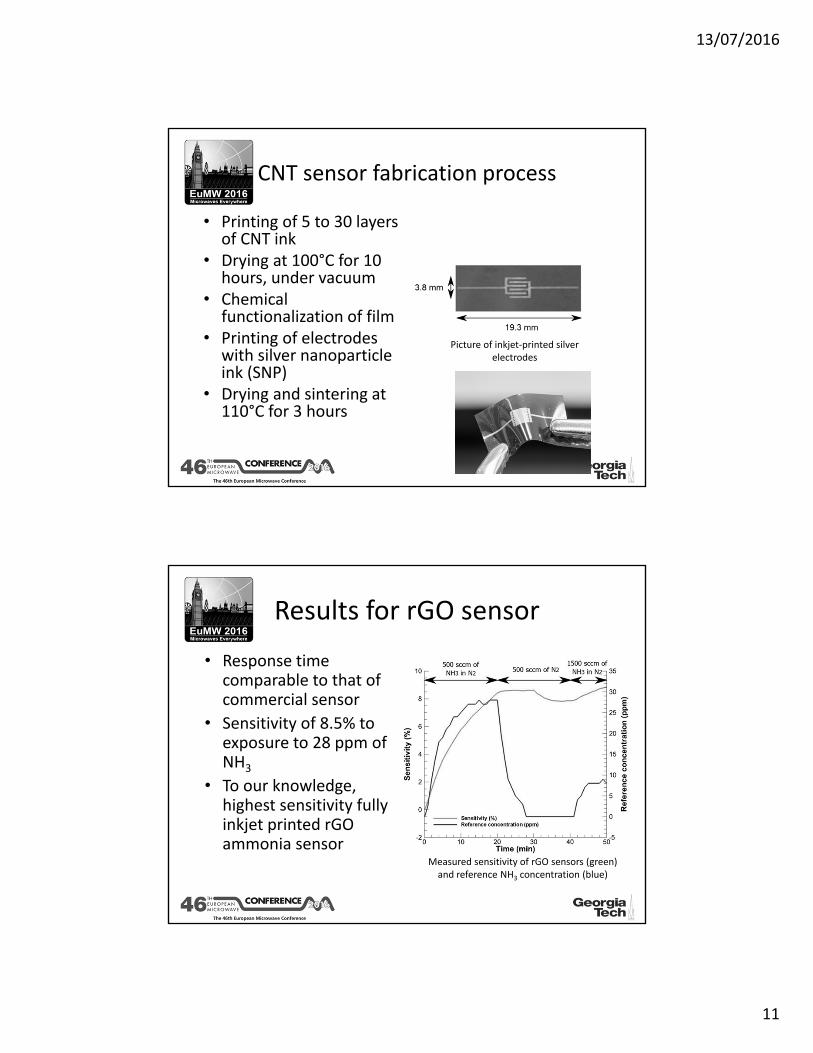
• Printing of 5 to 30 layers of CNT ink
• Drying at 100°C for 10 hours, under vacuum
• Chemical functionalization of film
• Printing of electrodes with silver nanoparticle ink (SNP)
• Drying and sintering at 110°C for 3 hours
CNT sensor fabrication process
Picture of inkjet‐printed silver electrodes
• Response time comparable to that of commercial sensor
• Sensitivity of 8.5% to exposure to 28 ppm of NH3
• To our knowledge, highest sensitivity fully inkjet printed rGOammonia sensor
Results for rGO sensor
Measured sensitivity of rGO sensors (green) and reference NH3 concentration (blue)
13/07/2016
12
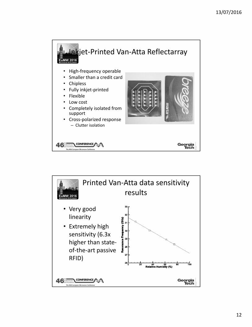
• High‐frequency operable• Smaller than a credit card• Chipless• Fully inkjet‐printed• Flexible• Low cost• Completely isolated from
support• Cross‐polarized response
– Clutter isolation
Inkjet‐Printed Van‐Atta Reflectarray
• Very good linearity
• Extremely high sensitivity (6.3x higher than state‐of‐the‐art passive RFID)
Printed Van‐Atta data sensitivity results
13/07/2016
13
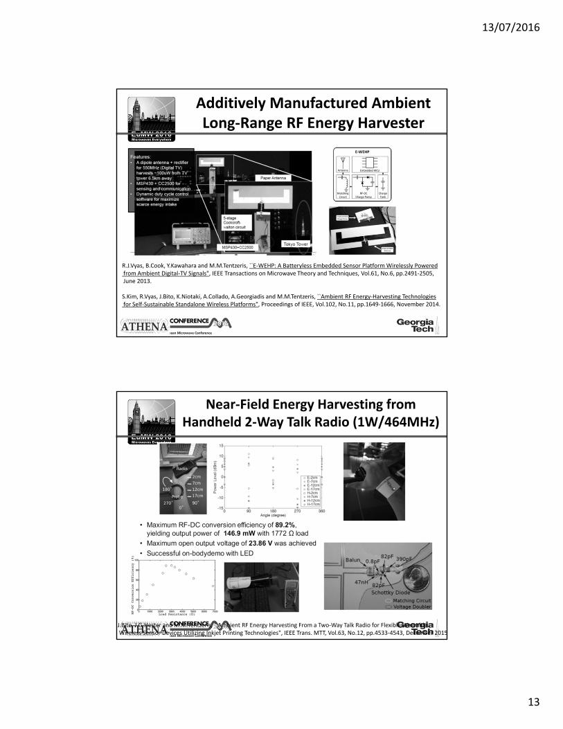
Additively Manufactured Ambient Long‐Range RF Energy Harvester
R.J.Vyas, B.Cook, Y.Kawahara and M.M.Tentzeris, ``E‐WEHP: A Batteryless Embedded Sensor Platform Wirelessly Poweredfrom Ambient Digital‐TV Signals", IEEE Transactions on Microwave Theory and Techniques, Vol.61, No.6, pp.2491‐2505,June 2013.
S.Kim, R.Vyas, J.Bito, K.Niotaki, A.Collado, A.Georgiadis and M.M.Tentzeris, ``Ambient RF Energy‐Harvesting Technologiesfor Self‐Sustainable Standalone Wireless Platforms", Proceedings of IEEE, Vol.102, No.11, pp.1649‐1666, November 2014.
Near‐Field Energy Harvesting from Handheld 2‐Way Talk Radio (1W/464MHz)
J.Bito, J.G.Hester and M.M.Tentzeris, ``Ambient RF Energy Harvesting From a Two‐Way Talk Radio for Flexible WearableWireless Sensor Devices Utilizing Inkjet Printing Technologies", IEEE Trans. MTT, Vol.63, No.12, pp.4533‐4543, December 2015
13/07/2016
14
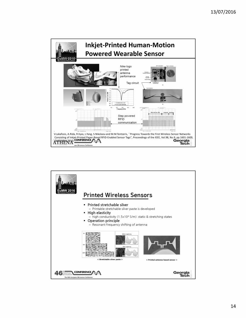
.V.Lakafosis, A.Rida, R.Vyas, L.Yang, S.Nikolaou and M.M.Tentzeris, ``Progress Towards the First Wireless Sensor NetworksConsisting of Inkjet‐Printed Paper‐Based RFID‐Enabled Sensor Tags", Proceedings of the IEEE, Vol.98, No.9, pp.1601‐1609,September 2010.
Inkjet‐Printed Human‐Motion Powered Wearable Sensor
13/07/2016
15
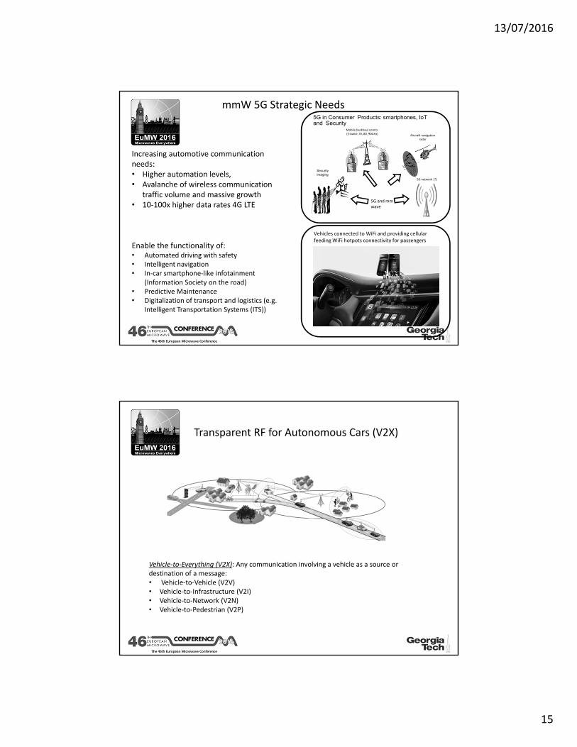
mmW 5G Strategic Needs
Vehicles connected to WiFi and providing cellular feeding WiFi hotpots connectivity for passengers
5G in Consumer Products: smartphones, IoTand Security
Security imaging
Aircraft navigation radar
Mobile backhaul comm.(E‐band: 70, 80, 90GHz)
5G network [*]
5G and mm wave
Increasing automotive communication needs:• Higher automation levels,• Avalanche of wireless communication
traffic volume and massive growth • 10‐100x higher data rates 4G LTE
Enable the functionality of:• Automated driving with safety• Intelligent navigation• In‐car smartphone‐like infotainment
(Information Society on the road)• Predictive Maintenance• Digitalization of transport and logistics (e.g.
Intelligent Transportation Systems (ITS))
Transparent RF for Autonomous Cars (V2X)
Vehicle‐to‐Everything (V2X): Any communication involving a vehicle as a source or destination of a message:• Vehicle‐to‐Vehicle (V2V)• Vehicle‐to‐Infrastructure (V2I)• Vehicle‐to‐Network (V2N)• Vehicle‐to‐Pedestrian (V2P)
07/07/2016
1
Slide 1of Tauno V-H
Millimetre Wave MCM Technologiesfor Communication and Sensing
Tauno Vähä-Heikkilä
VTT, MilliLab
WM08 Advances in Millimetre-Wave 3D Printing and MCM Technologies
Slide 2of Tauno V-H
• Background• Millimeter wave module technologies and
integration techniques• Antenna realizations• Summary
Outline
07/07/2016
2
Slide 3of Tauno V-H
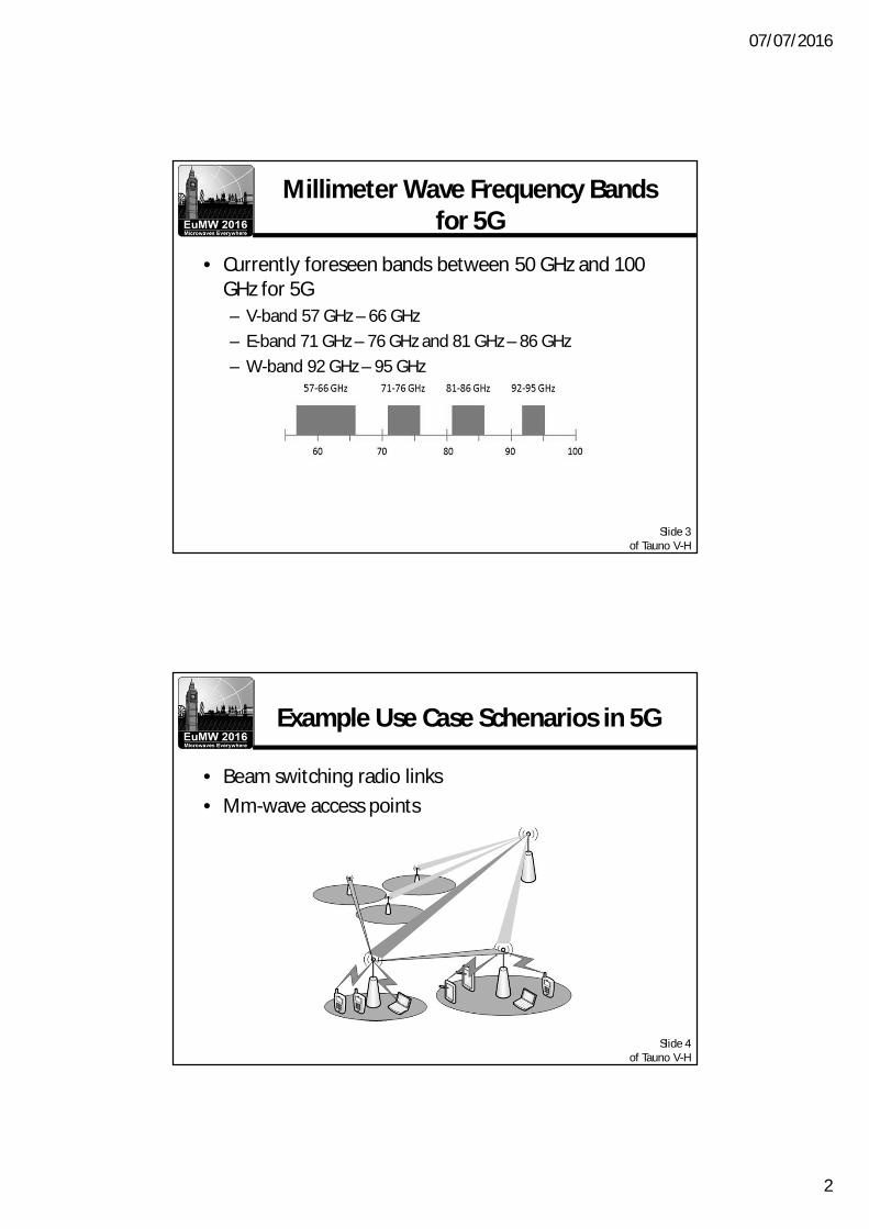
• Currently foreseen bands between 50 GHz and 100GHz for 5G– V-band 57 GHz – 66 GHz– E-band 71 GHz – 76 GHz and 81 GHz – 86 GHz– W-band 92 GHz – 95 GHz
Millimeter Wave Frequency Bandsfor 5G
Slide 4of Tauno V-H
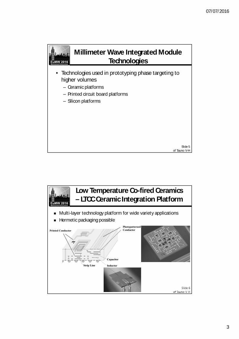
• Beam switching radio links• Mm-wave access points
Example Use Case Schenarios in 5G
07/07/2016
3
Slide 5of Tauno V-H
• Technologies used in prototyping phase targeting tohigher volumes– Ceramic platforms– Printed circuit board platforms– Silicon platforms
Millimeter Wave Integrated ModuleTechnologies
Slide 6of Tauno V-H
Low Temperature Co-fired Ceramics– LTCC Ceramic Integration Platform
n Multi-layer technology platform for wide variety applicationsn Hermetic packaging possible
07/07/2016
4
Slide 7of Tauno V-H
LTCC System-in-Packagen Packaging and integration technologyn Metallizations in several layers
n Vias between layersn Vias used for formimg EM sturctures like substrate integrated
waveguides, resonatorsn Several dielectric layers
n Can have cavities between the layersn Ceramic can be shaped to have 3D forms
Slide 8of Tauno V-H
LTCC as an Integration Platform forFront-End Modules and Filter Banks
LTCC can also be used inconsumer products
Source: www.epcos.com
07/07/2016
5
Slide 9of Tauno V-H
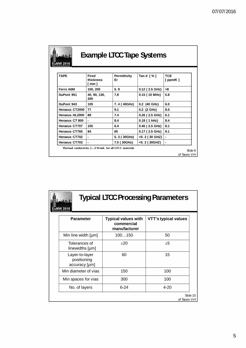
Example LTCC Tape Systems
TAPE Firedthickness[ mm ]
PermittivityEr
Tan d [ % ] TCE[ ppm/K ]
Ferro A6M 100, 200 5. 9 0.12 ( 2.5 GHz) >8
DuPont 951 40, 90, 130,200
7.8 0.15 ( 10 MHz) 5.8
DuPont 943 105 7. 4 ( 40GHz) 0.2 (40 GHz) 6.0
Heraeus CT2000 77 9.1 0.2 (2 GHz) 8.5
Heraeus HL2000 89 7.4 0.26 ( 2.5 GHz) 6.1
Heraeus CT 800 - 8.4 0.18 ( 1 kHz) 8.4
Heraeus CT707 105 6.4 0.46 ( 2.5 GHz) 8.1
Heraeus CT765 84 65 0.17 ( 2.5 GHz) 9.1
Heraeus CT702 - 5. 3 ( 30GHz) <0. 2 ( 30 GHZ) -
Heraeus CT703 - 7.0 ( 30GHz) <0. 2 ( 30GHZ) -
Thermal conductivity 2…4 W/mK for all LTCC materials
Slide 10of Tauno V-H
Typical LTCC Processing Parameters
Parameter Typical values withcommercial
manufacturer
VTT’s typical values
Min line width [µm] 100…150 50
Tolerances oflinewidths [µm]
±20 ±5
Layer-to-layerpositioning
accuracy [µm]
60 15
Min diameter of vias 150 100
Min spaces for vias 300 100
No. of layers 6-24 4-20
07/07/2016
6
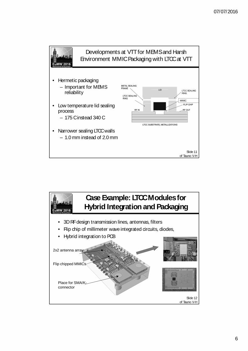
Slide 11of Tauno V-H
Developments at VTT for MEMS and HarshEnvironment MMIC Packaging with LTCC at VTT
• Hermetic packaging– Important for MEMS
reliability
• Low temperature lid sealingprocess– 175 C instead 340 C
• Narrower sealing LTCC walls– 1.0 mm instead of 2.0 mm
MMIC
Slide 12of Tauno V-H
Case Example: LTCC Modules forHybrid Integration and Packaging
• 3D RF design transmission lines, antennas, filters• Flip chip of millimeter wave integrated circuits, diodes,• Hybrid integration to PCB
2x2 antenna array
Flip chipped MMICs
Place for SMA/K-connector
07/07/2016
7
Slide 13of Tauno V-H
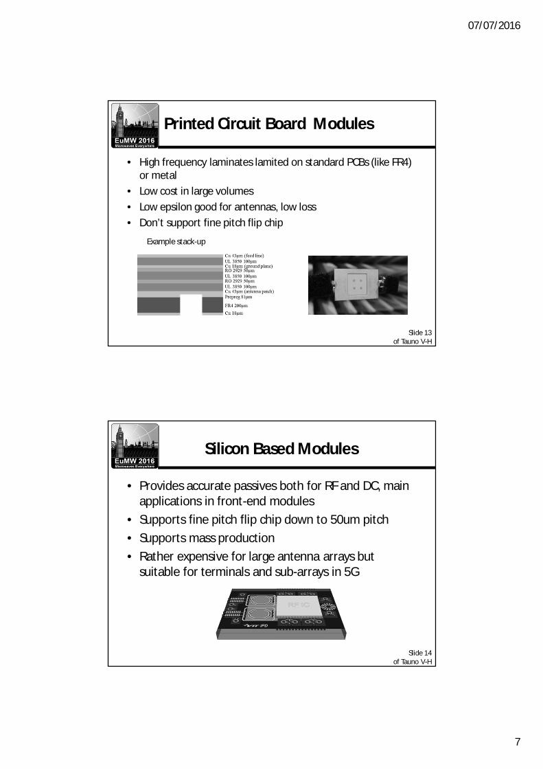
Printed Circuit Board Modules
• High frequency laminates lamited on standard PCBs (like FR4)or metal
• Low cost in large volumes• Low epsilon good for antennas, low loss• Don’t support fine pitch flip chip
Example stack-up
Slide 14of Tauno V-H
• Provides accurate passives both for RF and DC, mainapplications in front-end modules
• Supports fine pitch flip chip down to 50um pitch• Supports mass production• Rather expensive for large antenna arrays but
suitable for terminals and sub-arrays in 5G
Silicon Based Modules
07/07/2016
8
Slide 15of Tauno V-H
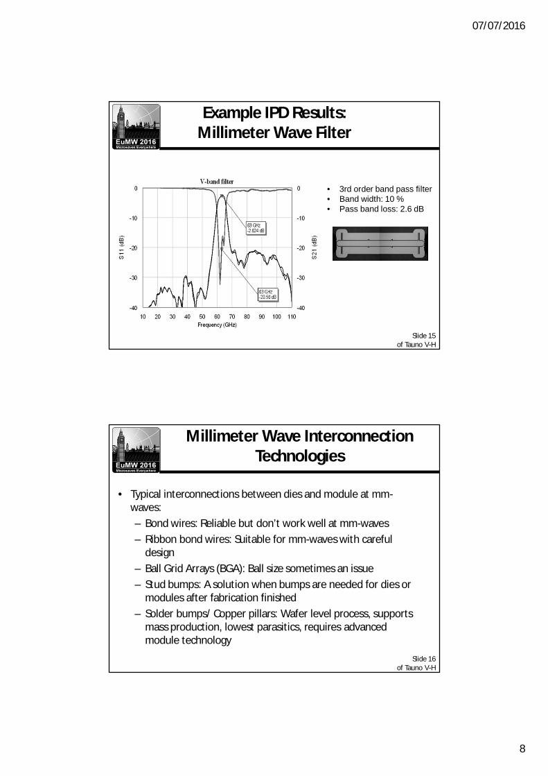
Example IPD Results:Millimeter Wave Filter
• 3rd order band pass filter• Band width: 10 %• Pass band loss: 2.6 dB
Slide 16of Tauno V-H
• Typical interconnections between dies and module at mm-waves:– Bond wires: Reliable but don’t work well at mm-waves– Ribbon bond wires: Suitable for mm-waves with careful
design– Ball Grid Arrays (BGA): Ball size sometimes an issue– Stud bumps: A solution when bumps are needed for dies or
modules after fabrication finished– Solder bumps/ Copper pillars: Wafer level process, supports
mass production, lowest parasitics, requires advancedmodule technology
Millimeter Wave InterconnectionTechnologies
07/07/2016
9
Slide 17of Tauno V-H
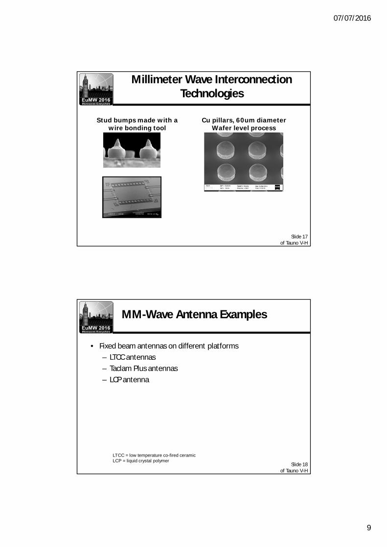
Millimeter Wave InterconnectionTechnologies
Cu pillars, 60um diameterWafer level process
Stud bumps made with awire bonding tool
Slide 18of Tauno V-H
MM-Wave Antenna Examples
• Fixed beam antennas on different platforms– LTCC antennas– Taclam Plus antennas– LCP antenna
LTCC = low temperature co-fired ceramicLCP = liquid crystal polymer
07/07/2016
10
Slide 19of Tauno V-H
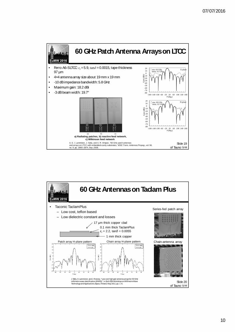
60 GHz Patch Antenna Arrays on LTCC
• Ferro A6-S LTCC: εr = 5.9, tanδ = 0.0015, tape thickness97 µm
• 4×4 antenna array size about 19 mm x 19 mm• -10 dB impedance bandwidth: 5.8 GHz• Maximum gain: 18.2 dBi• -3 dB beam width: 19.7°
A. E. I. Lamminen, J. Säily, and A. R. Vimpari, “60-GHz patch antennasand arrays on LTCC with embedded-cavity substrates,” IEEE Trans. Antennas Propag., vol. 56,no. 9, pp. 2865–2874, Sep. 2008.
θ (deg.)
Gai
n(d
Bi)
H-planesim. 60 GHzmeas. 61 GHz
-180 -140-100 -60 -20 20 60 100 140 180-80-70-60-50-40-30-20-10
01020
θ (deg.)
Gai
n(d
Bi)
sim. 60 GHzmeas. 61 GHz
E-plane
-180 -140 -100 -60 -20 20 60 100 140 180-80-70-60-50-40-30-20-10
01020
a) Radiating patches, b) reactive feed network,c) Wilkinson feed network
Slide 20of Tauno V-H
60 GHz Antennas on Taclam Plus
• Taconic TaclamPlus
– Low cost, teflon based
– Low dielectric constant and losses
17 μm thick copper clad
0.1 mm thick TaclamPlusεr = 2.2, tanδ = 0.0055
1 mm thick copper
Series-fed patch array
Chain-antenna arrayChain array H-plane patternPatch array H-plane pattern
J. Säily, A. Lamminen, and J. Francey, “Low cost high gain antenna arrays for 60 GHzmillimetre wave identification (MMID),” in Sixth ESA Workshop on Millimetre WaveTechnology and Applications, Espoo, Finland, May 2011, pp. 1–6.
07/07/2016
11
Slide 21of Tauno V-H
MM-Wave Antenna Examples
• Beam-switching antennas– 77 GHz end-fire antenna– 60 GHz integrated lens antenna
Slide 22of Tauno V-H
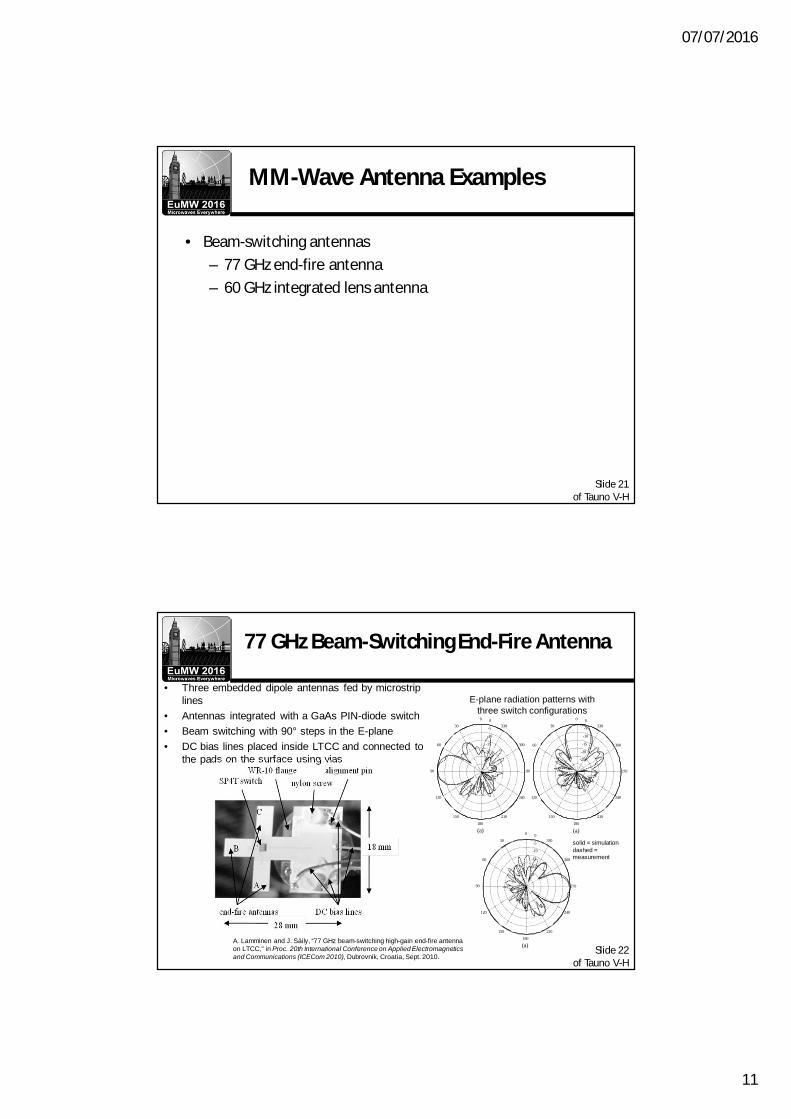
• Three embedded dipole antennas fed by microstriplines
• Antennas integrated with a GaAs PIN-diode switch
• Beam switching with 90° steps in the E-plane
• DC bias lines placed inside LTCC and connected tothe pads on the surface using vias
A. Lamminen and J. Säily, “77 GHz beam-switching high-gain end-fire antennaon LTCC,” in Proc. 20th International Conference on Applied Electromagneticsand Communications (ICECom 2010), Dubrovnik, Croatia, Sept. 2010.
-25
-20
-15
-10
-5
0
300
120
330
150
0
180
30
210
60
240
90
(a)
270
-25
-20
-15
-10
-5
0
300
120
330
150
0
180
30
210
60
240
90
(a)
-25
-20
-15
-10
-5
0
300
120
330
150
0
180
30
210
60
240
90 270
(a)
77 GHz Beam-Switching End-Fire Antenna
solid = simulationdashed =measurement
E-plane radiation patterns withthree switch configurations
07/07/2016
12
Slide 23of Tauno V-H
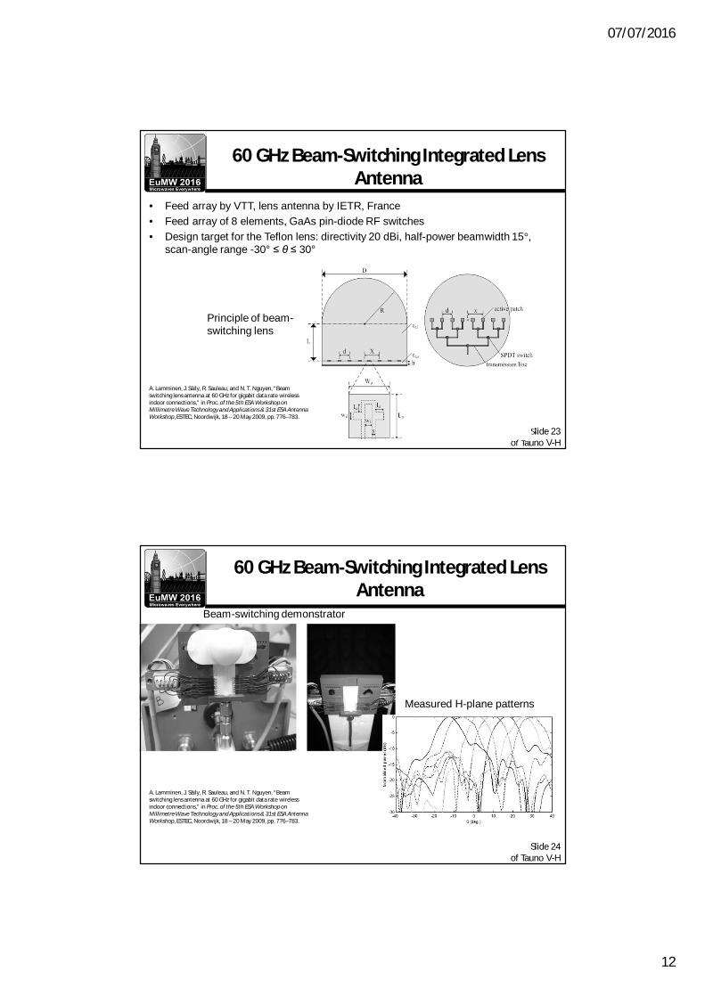
60 GHz Beam-Switching Integrated LensAntenna
• Feed array by VTT, lens antenna by IETR, France
• Feed array of 8 elements, GaAs pin-diode RF switches
• Design target for the Teflon lens: directivity 20 dBi, half-power beamwidth 15°,scan-angle range -30° ≤ θ ≤ 30°
Principle of beam-switching lens
A. Lamminen, J. Säily, R. Sauleau, and N. T. Nguyen, “Beamswitching lens antenna at 60 GHz for gigabit data rate wirelessindoor connections,” in Proc. of the 5th ESA Workshop onMillimetre Wave Technology and Applications & 31st ESA AntennaWorkshop, ESTEC, Noordwijk, 18 – 20 May 2009, pp. 776–783.
Slide 24of Tauno V-H
Beam-switching demonstrator
Measured H-plane patterns
60 GHz Beam-Switching Integrated LensAntenna
A. Lamminen, J. Säily, R. Sauleau, and N. T. Nguyen, “Beamswitching lens antenna at 60 GHz for gigabit data rate wirelessindoor connections,” in Proc. of the 5th ESA Workshop onMillimetre Wave Technology and Applications & 31st ESA AntennaWorkshop, ESTEC, Noordwijk, 18 – 20 May 2009, pp. 776–783.
07/07/2016
13
Slide 25of Tauno V-H
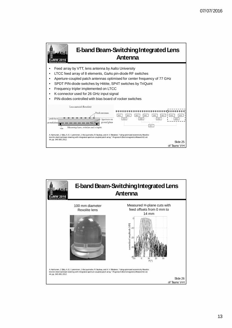
E-band Beam-Switching Integrated LensAntenna
• Feed array by VTT, lens antenna by Aalto University
• LTCC feed array of 8 elements, GaAs pin-diode RF switches
• Aperture-coupled patch antennas optimised for center frequency of 77 GHz
• SPDT PIN-diode switches by Hittite, SP4T switches by TriQuint
• Frequency tripler implemented on LTCC
• K-connector used for 26 GHz input signal
• PIN-diodes controlled with bias board of rocker switches
A. Karttunen, J. Säily, A. E. I. Lamminen, J. Ala-Laurinaho, R. Sauleau, and A. V. Räisänen, “Using optimized eccentricity Rexolitelens for electrical beam steering with integrated aperture coupled patch array,” Progress In Electromagnetics Research B, vol.44, pp. 345-365, 2012.
Slide 26of Tauno V-H
E-band Beam-Switching Integrated LensAntenna
100 mm diameterRexolite lens
Measured H-plane cuts withfeed offsets from 0 mm to
14 mm
A. Karttunen, J. Säily, A. E. I. Lamminen, J. Ala-Laurinaho, R. Sauleau, and A. V. Räisänen, “Using optimized eccentricity Rexolitelens for electrical beam steering with integrated aperture coupled patch array,” Progress In Electromagnetics Research B, vol.44, pp. 345-365, 2012.
07/07/2016
14
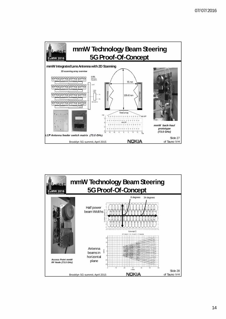
Slide 27of Tauno V-H
mmW Technology Beam Steering5G Proof-Of-Concept
LCP Antenna feeder switch matrix (73.5 GHz)
mmW back-haulprototype(73.5 GHz)
mmW Integrated Lens Antenna with 2D Scanning
Brooklyn 5G summit, April 2015
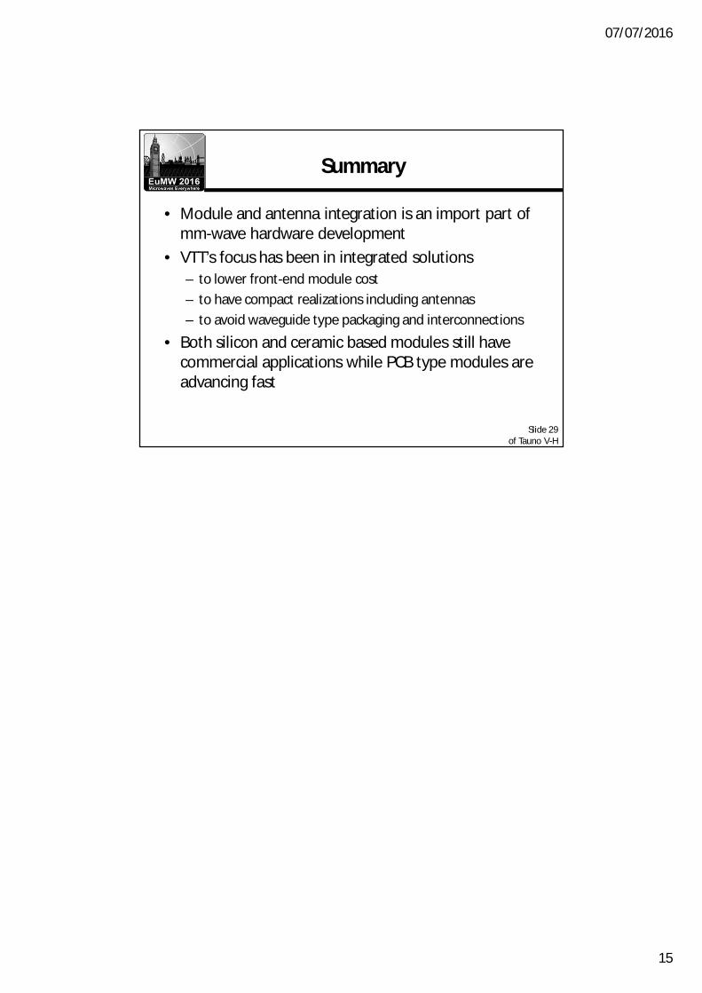
Slide 28of Tauno V-H
mmW Technology Beam Steering5G Proof-Of-Concept
8 degrees 34 degrees
Half powerbeam Widths
Access Point mmWRF Node (73.5 GHz)
Antennabeams inhorizontal
plane
Brooklyn 5G summit, April 2015
07/07/2016
15
Slide 29of Tauno V-H
• Module and antenna integration is an import part ofmm-wave hardware development
• VTT’s focus has been in integrated solutions– to lower front-end module cost– to have compact realizations including antennas– to avoid waveguide type packaging and interconnections
• Both silicon and ceramic based modules still havecommercial applications while PCB type modules areadvancing fast
Summary