Embed Size (px)
Citation preview

Rev. 1.2 8/03 Copyright © 2003 by Silicon Laboratories Aero+
Aero+
AERO™+ TRANSCEIVERFOR GSM AND GPRS WIRELESS COMMUNICATIONS
Features
Applications
Description
The Aero™+ transceiver is a complete RF front end for multi-band GSMand GPRS wireless communications. No external IF SAW filter or VCOmodules are required as all functions are completely implemented on-chip, resulting in a dramatic reduction of board area and componentcount. The Aero+ transceiver includes a digitally-controlled crystaloscillator (DCXO) that completely integrates the reference oscillator andvaractor.
Functional Block Diagram
Low-IF receiver:Dual or triple-band LNAImage-reject down-converter
Universal baseband interface:Digital IF to baseband converterChannel filter and gain controlAnalog or digital I/Q interface
Offset-PLL transmitter:Integrated TX VCO and loop filter
Dual RF synthesizer:Integrated RF and IF VCOs, loop filters, varactors, and resonators
Integrated reference oscillator:13 or 26 MHz operation
Quad-band support:GSM 850 Class 4, small MSE-GSM 900 Class 4, small MSDCS 1800 Class 1PCS 1900 Class 1
GPRS Class 12 compliantCMOS process technologyLow profile packages:
Si4200: 5 x 5 mm MLP32Si4201: 4 x 4 mm MLP20Si4134T: 5 x 5 mm MLP32
3-wire serial interface2.7 V to 3.0 V operation
Multi-band GSM/GPRS digital cellular handsetsMulti-band GPRS data modems and terminals
ADC
ADC
PGA
PGALNA
LNA
LNA
Si4200
IFPLL
RFPLL
Si4134T
GSM
DCS
PCS
GSM
DCSPCS
DCXO
0 / 90
ANTE
NNA S
WIT
CH
φDET
BASE
BAND
DAC
DAC
PGA
PGACHAN
NEL
FILT
ER
100 kHz
Si4201I
Q
I
Q
PA
PA
AFC
XOUT
Patents pending
Pin Assignments(Top View)Si4200-BM
(Si4200DB-BM see page 39)
Si4201-BM
Si4134T-BM
Ordering Information: See page 42.
GNDPAD
1
2
3
2526272829303132ION
IOP
TXQN
TXQP
CKN
CKP
TXIN
TXIP
IFLO
P
IFLO
N
GND
RFLO
P
RFLO
N
VDD
DIAG
2
DIAG
1
V DD PDN
GND
NC NC GND
VDD
RFOG
RFIDP
RFIDN
RFIPP
RFIPN
RFIGP
RFIGN
VDD
RFOD
17
18
19
20
21
22
23
24
9 10 11 12 13 14 15 16
4
5
6
7
8
GNDPAD
1
2
3
1617181920GND
RXQP
RXQN
RXIP
RXINVD
D
XIN
GND
CKP
CKN
V DD XOUT
SDI
SCLK
SEN
IOP
ION
XEN
PDN
SDO
11
12
13
14
15
6 7 8 9 10
4
5
GNDPAD
1
2
3
2526272829303132IFLB
IFLA
GND
VDD
PDN
XDRVEN
GND
XDRV
NC NC
XTAL
1
XTAL
2
XTAL
EN
XAFC SE
N
SCLK
GND
V DD IFLO
P
IFLO
N
VDD
RFLO
P
RFLO
N
GND
GND
RFLD
SDI
SDO
RFLC
GND
NC
GND
17
18
19
20
21
22
23
24
9 10 11 12 13 14 15 16
4
5
6
7
8
Aero+
2 Rev. 1.2

Aero+
Rev. 1.2 3
TABLE OF CONTENTS
Section Page
Electrical Specifications . . . . . . . . . . . . . . . . . . . . . . . . . . . . . . . . . . . . . . . . . . . . . . . . . . . . .4Typical Triple-Band Application Schematic . . . . . . . . . . . . . . . . . . . . . . . . . . . . . . . . . . . .16Bill of Materials . . . . . . . . . . . . . . . . . . . . . . . . . . . . . . . . . . . . . . . . . . . . . . . . . . . . . . . . . . . .17Functional Description . . . . . . . . . . . . . . . . . . . . . . . . . . . . . . . . . . . . . . . . . . . . . . . . . . . . .18
Receive Section . . . . . . . . . . . . . . . . . . . . . . . . . . . . . . . . . . . . . . . . . . . . . . . . . . . . . . . .19Transmit Section . . . . . . . . . . . . . . . . . . . . . . . . . . . . . . . . . . . . . . . . . . . . . . . . . . . . . . .20Frequency Synthesizer . . . . . . . . . . . . . . . . . . . . . . . . . . . . . . . . . . . . . . . . . . . . . . . . . .21VCO Inductor Design . . . . . . . . . . . . . . . . . . . . . . . . . . . . . . . . . . . . . . . . . . . . . . . . . . . .22DCXO Overview . . . . . . . . . . . . . . . . . . . . . . . . . . . . . . . . . . . . . . . . . . . . . . . . . . . . . . . .23Serial Interface . . . . . . . . . . . . . . . . . . . . . . . . . . . . . . . . . . . . . . . . . . . . . . . . . . . . . . . . .24XDRV Buffer . . . . . . . . . . . . . . . . . . . . . . . . . . . . . . . . . . . . . . . . . . . . . . . . . . . . . . . . . . .24XOUT Buffer . . . . . . . . . . . . . . . . . . . . . . . . . . . . . . . . . . . . . . . . . . . . . . . . . . . . . . . . . . .24
Control Registers . . . . . . . . . . . . . . . . . . . . . . . . . . . . . . . . . . . . . . . . . . . . . . . . . . . . . . . . . .25Pin Descriptions: Si4200-BM . . . . . . . . . . . . . . . . . . . . . . . . . . . . . . . . . . . . . . . . . . . . . . . . .38Pin Descriptions: Si4200DB-BM . . . . . . . . . . . . . . . . . . . . . . . . . . . . . . . . . . . . . . . . . . . . . .39Pin Descriptions: Si4201-BM . . . . . . . . . . . . . . . . . . . . . . . . . . . . . . . . . . . . . . . . . . . . . . . . .40Pin Descriptions: Si4134T-BM . . . . . . . . . . . . . . . . . . . . . . . . . . . . . . . . . . . . . . . . . . . . . . .41Ordering Guide . . . . . . . . . . . . . . . . . . . . . . . . . . . . . . . . . . . . . . . . . . . . . . . . . . . . . . . . . . . .42Package Outline: Si4200-BM and Si4200DB-BM . . . . . . . . . . . . . . . . . . . . . . . . . . . . . . . . .43Package Outline: Si4201-BM . . . . . . . . . . . . . . . . . . . . . . . . . . . . . . . . . . . . . . . . . . . . . . . . .44Package Outline: Si4134T-BM . . . . . . . . . . . . . . . . . . . . . . . . . . . . . . . . . . . . . . . . . . . . . . . .45Document Change List . . . . . . . . . . . . . . . . . . . . . . . . . . . . . . . . . . . . . . . . . . . . . . . . . . . . .46Contact Information . . . . . . . . . . . . . . . . . . . . . . . . . . . . . . . . . . . . . . . . . . . . . . . . . . . . . . . .48
Aero+
4 Rev. 1.2
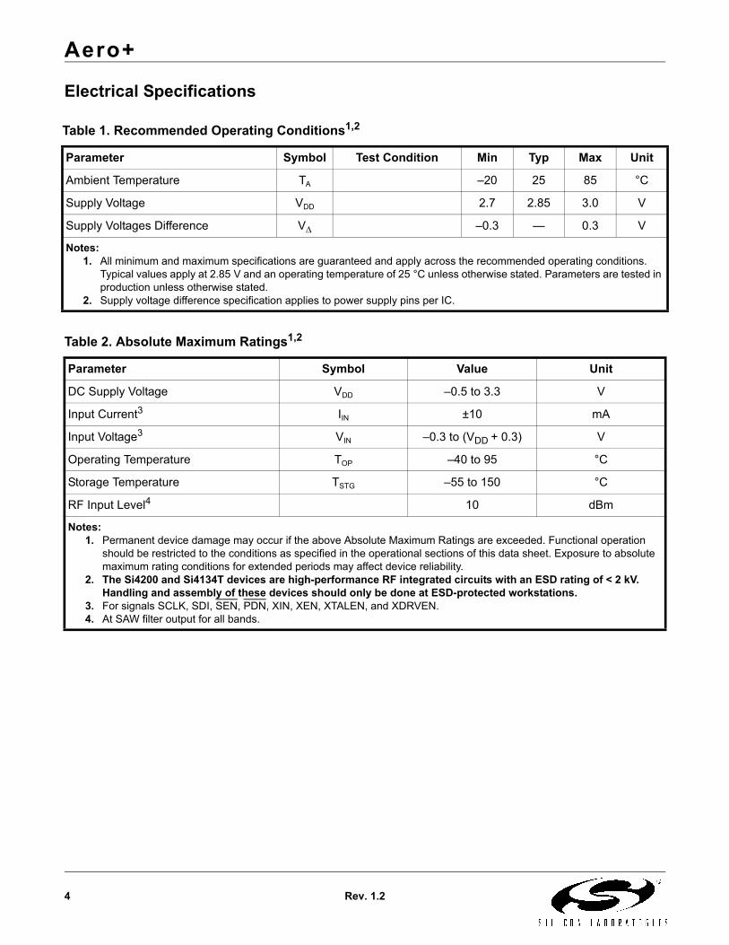
Electrical Specifications
Table 1. Recommended Operating Conditions1,2
Parameter Symbol Test Condition Min Typ Max Unit
Ambient Temperature TA –20 25 85 °C
Supply Voltage VDD 2.7 2.85 3.0 V
Supply Voltages Difference V∆ –0.3 — 0.3 V
Notes:1. All minimum and maximum specifications are guaranteed and apply across the recommended operating conditions.
Typical values apply at 2.85 V and an operating temperature of 25 °C unless otherwise stated. Parameters are tested in production unless otherwise stated.
2. Supply voltage difference specification applies to power supply pins per IC.
Table 2. Absolute Maximum Ratings1,2
Parameter Symbol Value Unit
DC Supply Voltage VDD –0.5 to 3.3 V
Input Current3 IIN ±10 mA
Input Voltage3 VIN –0.3 to (VDD + 0.3) V
Operating Temperature TOP –40 to 95 °C
Storage Temperature TSTG –55 to 150 °C
RF Input Level4 10 dBm
Notes:1. Permanent device damage may occur if the above Absolute Maximum Ratings are exceeded. Functional operation
should be restricted to the conditions as specified in the operational sections of this data sheet. Exposure to absolute maximum rating conditions for extended periods may affect device reliability.
2. The Si4200 and Si4134T devices are high-performance RF integrated circuits with an ESD rating of < 2 kV. Handling and assembly of these devices should only be done at ESD-protected workstations.
3. For signals SCLK, SDI, SEN, PDN, XIN, XEN, XTALEN, and XDRVEN.4. At SAW filter output for all bands.

Aero+
Rev. 1.2 5
Table 3. DC Characteristics(VDD = 2.7 to 3.0 V, TA = –20 to 85 °C)
Parameter Symbol Test Condition Min Typ Max Unit
Si4200 Supply Current IRX0 Receive mode — 55 80 mA
ITX0 Transmit mode — 60 80 mA
IPDN0 PDN = 0 — 1 50 µA
Si4201 Supply Current1 IRX1 Receive mode — 9 12 mA
IPDN1 PDN = 0, XEN = 0,XBUF = 0, XPD1 = 1
— 1 50 µA
IXOUT1 PDN = 0, XEN = 1 — 1 2 mA
Si4134T Supply Current2 IRX3 Receive mode — 18 22 mA
ITX3 Transmit mode — 24 30 mA
IPDN3 PDN = 0, XTALEN = 0 — 1 50 µA
IXTAL13 PDN = 0, XTALEN = 1, fREF = 13 MHz
— 2.5 3.5 mA
IXTAL26 PDN = 0, XTALEN = 1, fREF = 26 MHz
— 3.0 4.0 mA
Total Chipset Supply Current IRX Receive mode — 83 — mA
ITX Transmit mode — 85 — mA
High Level Input Voltage3 VIH 0.7 VDD — — V
Low Level Input Voltage3 VIL — — 0.3 VDD V
High Level Input Current3 IIH VIH = VDD = 3.0 V –10 — 10 µA
Low Level Input Current3 IIL VIL = 0 V, VDD = 3.0 V
–10 — 10 µA
High Level Output Voltage4 VOH IOH = –500 µA VDD–0.4 — — V
Low Level Output Voltage4 VOL IOL = 500 µA — — 0.4 V
High Level Output Voltage5 VOH IOH = –10 mA VDD–0.4 — — V
Low Level Output Voltage5 VOL IOL = 10 mA — — 0.4 V
Notes:1. Measured with load on XOUT pin of 10 pF and fREF = 13 MHz. Limits with XEN = 1 guaranteed by characterization.2. RF1 VCO is used for receive mode, RF2 and IF VCOs are used for transmit mode. Center frequencies for each VCO
are as follows: RF1 = 1.9 GHz, RF2 = 1.35 GHz, IF = 825 MHz, fREF = 13 MHz. 3. For pins SCLK, SDI, SEN, XEN, PDN, XDRVEN, and XTALEN.4. For pins SDO and XOUT.5. For pins DIAG1 and DIAG2.

Aero+
6 Rev. 1.2
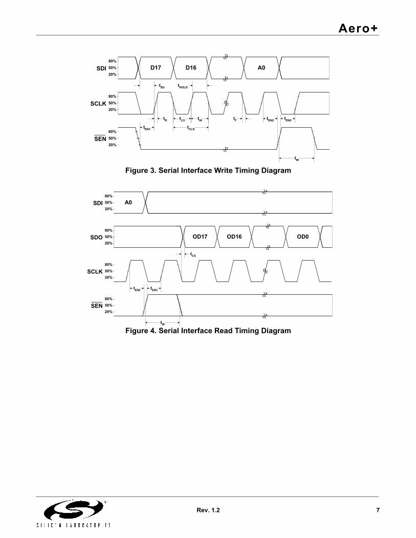
Figure 1. SCLK Timing Diagram
Figure 2. PDN Timing Diagram
Table 4. AC Characteristics(VDD = 2.7 to 3.0 V, TA = –20 to 85 °C)
Parameter Symbol Test Condition Min Typ Max UnitSCLK Cycle Time tCLK Figure 1, Figure 3 35 — — nsSCLK Rise Time tR Figure 1, Figure 3 — — 50 nsSCLK Fall Time tF Figure 1, Figure 3 — — 50 nsSCLK High Time tHI Figure 1, Figure 3 10 — — nsSCLK Low Time tLO Figure 1, Figure 3 10 — — nsPDN Rise Time tPR Figure 2 — — 10 nsPDN Fall Time tPF Figure 2 — — 10 nsSDI Setup Time to SCLK↑ tSU Figure 3 15 — — nsSDI Hold Time from SCLK↑ tHOLD Figure 3 10 — — nsSEN↓ to SCLK↑ Delay Time tEN1 Figure 3 10 — — nsSCLK↑ to SEN↑ Delay Time tEN2 Figure 3, Figure 4 12 — — nsSEN↑ to SCLK↑ Delay Time tEN3 Figure 3, Figure 4 12 — — nsSEN Pulse Width tW Figure 3, Figure 4 10 — — nsSCLK↓ to SDO Time tCA Figure 4 — — 27 nsDigital Input Pin Capacitance1 — — 5 pFAllowable Board Capacitance2 — — 1 pFNotes:
1. For pins SCLK, SDI, SEN, XEN, PDN, XDRVEN, and XTALEN.2. For pins CKN, CKP, ION, and IOP.
SCLK80%
20%50%
tR tF
tLOtCLK
tHI
PDN80%
20%
tPR tPF
Aero+
Rev. 1.2 7
Figure 3. Serial Interface Write Timing Diagram
Figure 4. Serial Interface Read Timing Diagram
tEN1
80%50%20%
80%50%20%
80%50%20%
D17 D16 A0
tR
tW
tEN2tFtLO tHI
tCLK
tHOLDtSU
SDI
SCLK
SEN
tEN3
80%50%20%
80%50%20%
80%50%20%
A0
80%50%20%
SDI
SCLK
SEN
SDO OD17 OD0OD16
tCA
tEN2 tEN3
tW

Aero+
8 Rev. 1.2
Table 5. Receiver Characteristics (VDD = 2.7 to 3.0 V, TA = –20 to 85 °C)
Parameter Symbol Test Condition Min Typ Max UnitGSM Input Frequency1 FIN GSM 850 band 869 — 894 MHz
E-GSM 900 band 925 — 960 MHzDCS or PCS Input Frequency1 DCS 1800 band 1805 — 1880 MHz
PCS 1900 band 1930 — 1990 MHzNoise Figure at 25 °C2,3 NF25 GSM 850 band — 2.6 3.3 dB
E-GSM 900 band — 2.7 3.4 dBDCS 1800 band — 3.2 3.9 dBPCS 1900 band — 3.6 4.3 dB
Noise Figure at 75 °C2,3 NF75 GSM 850 band — 3.3 4.0 dBE-GSM 900 band — 3.4 4.1 dBDCS 1800 band — 4.1 4.8 dBPCS 1900 band — 4.8 5.5 dB
Noise Figure at 85 °C2,3 NF85 GSM 850 band — 3.4 4.1 dBE-GSM 900 band — 3.5 4.2 dBDCS 1800 band — 4.5 5.2 dBPCS 1900 band — 5.1 5.8 dB
3 MHz Input Desensitization2,3,4 DES3 GSM input –25 –21 — dBmDCS/PCS inputs –28 –25 — dBm
20 MHz Input Desensitization2,3,4 DES20 GSM input –20 –16 — dBmDCS/PCS inputs –19 –15 — dBm
Input IP22 IP2 |f1,2 – f0| ≥ 6 MHz, |f2 – f1| = 100 kHz
29 40 — dBm
Input IP32 IP3 |f2 – f1| ≥ 800 kHz, f0 = 2f1 – f2
–18 –12 — dBm
Image Rejection2,4 IR GSM Input 28 35 — dBDCS/PCS Inputs 28 40 — dB
1 dB Input Compression2,5 CPMAX GSM Input –28 –23 — dBmDCS/PCS inputs –27 –22 — dBm
1 dB Input Compression2,6 CPMIN GSM Input –23 –18 — dBmDCS/PCS inputs –23 –18 — dBm
Minimum Voltage Gain2,6,7 GMIN GSM input 4.5 8.5 12.5 dBDCS/PCS inputs 11.5 15.5 19.5 dB
Maximum Voltage Gain2,7 GMAX GSM input 100 104 108 dBDCS/PCS inputs 96 102 106 dB
LNA Voltage Gain3,8 GLNA GSM input — 17 — dBDCS/PCS inputs — 15 — dB
Aero+
Rev. 1.2 9
LNA Gain Control Range ∆GLNA GSM input 13 17 21 dBDCS/PCS inputs 4 8 12 dB
Analog PGA Control Range ∆GAPGA 13 16 19 dBAnalog PGA Step Size 3.2 4.0 4.8 dBDigital PGA Control Range ∆GDPGA — 63 — dBDigital PGA Step Size — 1 — dBMaximum Differential Output Voltage9 DACFS[1:0] = 00 0.8 1.0 1.2 VPPD
DACFS[1:0] = 01 1.6 2.0 2.4 VPPD
DACFS[1:0] = 10 2.8 3.5 4.2 VPPD
Output Common Mode Voltage9 DACCM[1:0] = 00 0.8 1.0 1.2 VDACCM[1:0] = 01 1.05 1.25 1.45 VDACCM[1:0] = 10 1.15 1.35 1.55 V
Differential Output Offset Voltage9,10 — — 50 mVBaseband Gain Error9,10 — — 1 %Baseband Phase Error9,10 — — 1 degOutput Load Resistance9 RL Single-ended 10 — — kΩ
Output Load Capacitance9 CL Single-ended — — 10 pFGroup Delay11 CSEL = 0 — — 22 µs
CSEL = 1 — — 16 µsDifferential Group Delay11 CSEL = 0 — — 1.5 µs
CSEL = 1 — — 1 µsPowerup Settling Time3,12 From powerdown — 200 220 µsNotes:
1. GSM input pins RFIGP and RFIGN. DCS input pins RFIDP and RFIDN. PCS input pins RFIPP and RFIPN. On the Si4200DB, the PCS input should be used for either PCS 1900 or DCS 1800 bands.
2. Measurement is performed with a 2:1 balun (50 Ω input, 200 Ω balanced output) and includes matching network and PCB losses. Measured at max gain (AGAIN[2:0] =100b, LNAG[1:0] = 01b, LNAC[1:0] = 01b) unless otherwise noted. Noise figure measurements are referred to 290 °K. Insertion loss of the balun is removed.
3. Specifications guaranteed by characterization.4. Input signal at balun is –102 dBm. SNR at baseband output is 9 dB.5. AGAIN[2:0]=000b, LNAG[1:0] = 01b, LNAC[1:0] = 01b.6. AGAIN[2:0]=000b, LNAG[1:0] = 00b, LNAC[1:0] = 00b.7. Voltage gain is defined as the differential rms voltage at the RXIP/RXIN pins or RXQP/RXQN pins divided by the rms voltage at the
balun input with DACFS[1:0] = 01 and CSEL = 1. Gain is 1.5 dB higher with CSEL = 0. Minimum and maximum values do not include the variation in the Si4201 DAC full scale voltage (also see Maximum Differential Output Voltage specification).
8. Voltage gain is defined as the differential rms voltage at the LNA output divided by the rms voltage at the balun output.9. Output pins RXIP, RXIN, RXQP, RXQN. 10. The baseband signal path is entirely digital. Gain, phase, and offset errors at the baseband outputs are because of the Si4201 D/A
converters. Offsets can be measured and calibrated out. See ZERODEL[2:0] in the register description.11. Group delay is measured from antenna input to baseband outputs. Differential group delay is measured in-band.12. Includes settling time of the Si4134T frequency synthesizer with 13 MHz DCXO output settled. Settling to 5 degrees phase error
measured at RXIP, RXIN, RXQP, and RXQN pins.
Table 5. Receiver Characteristics (Continued)(VDD = 2.7 to 3.0 V, TA = –20 to 85 °C)
Parameter Symbol Test Condition Min Typ Max Unit
Aero+
10 Rev. 1.2
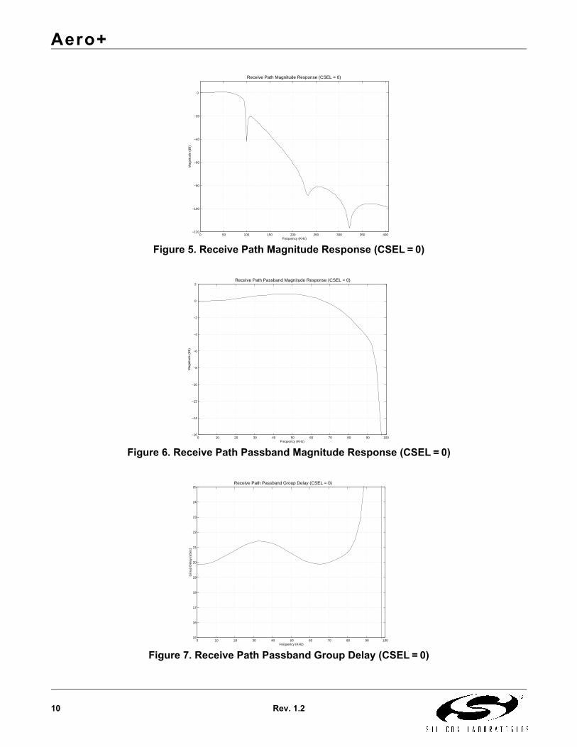
Figure 5. Receive Path Magnitude Response (CSEL = 0)
Figure 6. Receive Path Passband Magnitude Response (CSEL = 0)
Figure 7. Receive Path Passband Group Delay (CSEL = 0)
0 50 100 150 200 250 300 350 400−120
−100
−80
−60
−40
−20
0
Receive Path Magnitude Response (CSEL = 0)
Mag
nitu
de (
dB)
Frequency (KHz)
0 10 20 30 40 50 60 70 80 90 100−16
−14
−12
−10
−8
−6
−4
−2
0
2 Receive Path Passband Magnitude Response (CSEL = 0)
Mag
nitu
de (
dB)
Frequency (KHz)
0 10 20 30 40 50 60 70 80 90 10015
16
17
18
19
20
21
22
23
24
25Receive Path Passband Group Delay (CSEL = 0)
Gro
up D
elay
(uS
ec)
Frequency (KHz)

Aero+
Rev. 1.2 11
Figure 8. Receive Path Magnitude Response (CSEL = 1)
Figure 9. Receive Path Passband Magnitude Response (CSEL = 1)
Figure 10. Receive Path Passband Group Delay (CSEL = 1)
0 50 100 150 200 250 300 350 400 −80
−60
−40
−20
0
Receive Path Magnitude Response (CSEL = 1)
Mag
nitu
de (
dB)
Frequency (KHz)
0 10 20 30 40 50 60 70 80 90 100−16
−14
−12
−10
−8
−6
−4
−2
0
2 Receive Path Passband Magnitude Response (CSEL = 1)
Mag
nitu
de (
dB)
Frequency (KHz)
0 10 20 30 40 50 60 70 80 90 10010
11
12
13
14
15
16
17
18
19
20Receive Path Passband Group Delay (CSEL = 1)
Gro
up D
elay
(uS
ec)
Frequency (KHz)

Aero+
12 Rev. 1.2
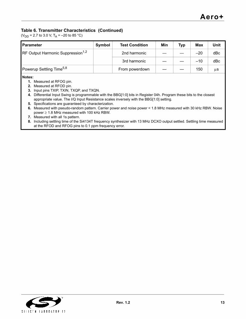
Table 6. Transmitter Characteristics (VDD = 2.7 to 3.0 V, TA = –20 to 85 °C)
Parameter Symbol Test Condition Min Typ Max Unit
RFOG Output Frequency1 GSM 850 band 824 — 849 MHz
E-GSM 900 band 880 — 915 MHz
RFOD Output Frequency2 DCS 1800 band 1710 — 1785 MHz
PCS 1900 band 1850 — 1910 MHz
I/Q Differential Input Swing3,4 0.88 — 2.2 VPPD
I/Q Input Common-Mode3 1.1 — 1.4 V
I/Q Differential Input Resistance3,4 BBG[1:0] = 11b 26 30 35 kΩ
BBG[1:0] = 00b 22 25 29 kΩ
BBG[1:0] = 01b 17 20 23 kΩ
Powered down — Hi-Z — kΩ
I/Q Input Capacitance3,5 — — 5 pF
I/Q Input Bias Current3 13 16 19 µA
Sideband Suppression 67.7 kHz sinusoid — –46 –34 dBc
Carrier Suppression 67.7 kHz sinusoid — –48 –33 dBc
IM3 Suppression 67.7 kHz sinusoid — –57 –50 dBc
Phase Error5 — 1.9 3.0 orms
— 5 10 oPEAK
TXVCO Pushing1,2 Open loop — 100 — kHz/V
TXVCO Pulling1,2 VSWR 2:1, all phases open loop
— 200 — kHzPP
RFOG Output Modulation Spectrum1,6 400 kHz offset — –65 –63 dBc
1.8 MHz offset — –70 –68 dBc
RFOD Output Modulation Spectrum2,6 400 kHz offset — –65 –63 dBc
1.8 MHz offset — –70 –65 dBc
RFOG Output Phase Noise1,5,7 10 MHz offset — –160 –155 dBc/Hz
20 MHz offset — –166 –164 dBc/Hz
RFOD Output Phase Noise2,5,7 20 MHz offset — –163 –157 dBc/Hz
RFOG Output Power Level1 ZL = 50 Ω 7 9 11 dBm
RFOD Output Power Level2 ZL = 50 Ω 6 8 10 dBm
Aero+
Rev. 1.2 13
RF Output Harmonic Suppression1,2 2nd harmonic — — –20 dBc
3rd harmonic — — –10 dBc
Powerup Settling Time5,8 From powerdown — — 150 µs
Notes:1. Measured at RFOG pin.2. Measured at RFOD pin.3. Input pins TXIP, TXIN, TXQP, and TXQN.4. Differential Input Swing is programmable with the BBG[1:0] bits in Register 04h. Program these bits to the closest
appropriate value. The I/Q Input Resistance scales inversely with the BBG[1:0] setting.5. Specifications are guaranteed by characterization.6. Measured with pseudo-random pattern. Carrier power and noise power < 1.8 MHz measured with 30 kHz RBW. Noise
power ≥ 1.8 MHz measured with 100 kHz RBW.7. Measured with all 1s pattern.8. Including settling time of the Si4134T frequency synthesizer with 13 MHz DCXO output settled. Settling time measured
at the RFOD and RFOG pins to 0.1 ppm frequency error.
Table 6. Transmitter Characteristics (Continued)(VDD = 2.7 to 3.0 V, TA = –20 to 85 °C)
Parameter Symbol Test Condition Min Typ Max Unit

Aero+
14 Rev. 1.2
Table 7. Frequency Synthesizer Characteristics(VDD = 2.7 to 3.0 V, TA = –20 to 85 °C)
Parameter Symbol Test Condition Min Typ Max Unit
RF1 VCO Frequency1 fRF1 GSM 850 band 1737.8 — 1787.8 MHz
E-GSM 900 band 1849.8 — 1919.8 MHz
DCS 1800 band 1804.9 — 1879.9 MHz
PCS 1900 band 1929.9 — 1989.9 MHz
RF2 VCO Frequency1 fRF2 GSM 850 band 1272 — 1297 MHz
E-GSM 900 1279 — 1314 MHz
DCS 1800 band 1327 — 1402 MHz
PCS 1900 band 1423 — 1483 MHz
IF VCO Frequency1 fIF GSM 850 band — 896 — MHz
E-GSM 900 band880–895 MHz900–915 MHz
— 798 — MHz
E-GSM 900 band895–900 MHz
— 790 — MHz
DCS 1800 band — 766 — MHz
PCS 1900 band — 854 — MHz
RF1 PLL Phase Detector UpdateFrequency
fφ GSM input, RFUP = 0
— 200 — kHz
DCS/PCS inputs,RFUP = 1
— 100 — kHz
IF and RF2 PLL Phase Detector Update Frequency
fφ — 200 — kHz
RF2 VCO Nominal Capacitance2,3 CNOM — 4.8 — pF
IF VCO Nominal Capacitance2,3 — 6.5 — pF
RF2 VCO Package Inductance2,3 LPKG — 2.0 — nH
IF VCO Package Inductance2,3 — 1.6 — nH
RF1 VCO Pushing3 Open Loop — 500 — kHz/V
RF2 VCO Pushing3 — 400 — kHz/V
IF VCO Pushing3 — 300 — kHz/V
RF1 VCO Pulling3 VSWR = 2:1, all phases, open loop
— 400 — kHzPP
RF2 VCO Pulling3 — 100 — kHzPP
IF VCO Pulling3 — 100 — kHzPP
RF1 PLL Phase Noise3 3 MHz offset — –144 –138 dBc/Hz
RF2 PLL Phase Noise3 400 kHz offset — –126 –121 dBc/Hz
IF PLL Phase Noise3 400 kHz offset — –128 –123 dBc/Hz

Aero+
Rev. 1.2 15
RF1 PLL Spurious3 3 MHz offset — –95 –83 dBc
RF2 PLL Spurious3 400 kHz offset — –80 –75 dBc
IF PLL Spurious3 400 kHz offset — –80 –70 dBc
Notes:1. For the GSM input, the RF1 VCO is divided by two on the Si4200. During transmit, the IF VCO is divided by two on the
Si4200. These tuning ranges are guaranteed provided the VCOs on the Si4134T are properly centered during the PC board design phase. See “AN49: Aero Transceiver PCB Layout Guidelines” for more information.
2. See "VCO Inductor Design" on page 22.3. Specifications are guaranteed by characterization.
Table 8. Reference Oscillator (DCXO) Characteristics(VDD = 2.7 to 3.0 V, TA = –20 to 85 °C)
Parameter Symbol Test Condition Min Typ Max Unit
XDRV Board Capacitance CXDRV — — 2 pF
XTAL1 Trace Capacitance1 CXTAL1 — 0.90 — pF
XTAL2 Trace Capacitance1 CXTAL2 — 0.63 — pF
Crystal Oscillation Frequency fREF XSEL = 0, DIV2 = 0 — 13 — MHz
XSEL = 1, DIV2 = 1 — 26 — MHz
Crystal Load Capacitance CL — 8 — pF
Crystal Sensitivity2 S — 22.5 — ppm/pF
Initial Crystal Frequency Offset ∆fOFF TA = 25 °C –10 — 10 ppm
Crystal Frequency Tolerance3 ∆fTOL –10 — 10 ppm
CDAC Range4 ∆fCDAC 20 — — ppm
CDAC Step Size4,5 — 1.0 1.5 ppm
CVAR Input Voltage VXAFC 0 — 2.5 V
CVAR Range4 ∆fCVAR VCTL = 0 to 2.5 V 20 30 60 ppm
Powerup Settling Time tDCXO VCTL = 1.25 V — 1.0 — ms
Notes:1. See “AN49: Aero Transceiver PCB Layout Guidelines” for suggested layout.2. Allowable manufacturing tolerance of ±10% from typical value.3. Crystal accuracy over temperature range.4. Specifications guaranteed when using a crystal that conforms to fREF = 13 MHz, CL = 8 pF, S = 22.5 ppm/pF,
∆fOFF = ±10 ppm, and ∆fTOL = ±10 ppm.5. Average step size over CDAC codes 0 to 63.
Table 7. Frequency Synthesizer Characteristics (Continued)(VDD = 2.7 to 3.0 V, TA = –20 to 85 °C)
Parameter Symbol Test Condition Min Typ Max Unit

Aero+
16 Rev. 1.2
Typical Triple-Band Application Schematic
Notes:1. Connect GND pad on bottom of U1–U3 to GND.2. All VDD pins may be fed from a single supply or regulator.3. For dual-band designs, the DCS LNA input pins (U1 pins 19–20) should be grounded. For a complete pinout, see "Pin
Descriptions: Si4200DB-BM" on page 39.4. See “AN49: Aero Transceiver PCB Layout Guidelines” for details on the following:
LNA matching network (C1–C6, L1–L3). Values should be custom tuned for a specific PCB layout and SAW filter to optimize performance.Differential traces between the SAW filters (Z1–Z3) and transceiver (U1) pins 17–22.Detailed SAW filter (Z1–Z3) requirements.L4 and PCB inductor trace L5 for frequency synthesizer (U3) pins 1–2 and 20–21.CKP/CKN and IOP/ION differential traces between transceiver (U1) pins 1–4 and baseband interface (U2) pins 9–12.X1 connection to U3 pins 11–12.
5. XEN, XDRVEN, and XTALEN are recommended to be tied together and controlled simultaneously.
VDD
VDDVDD VDD
VDD
VDD
VDDVDD
VDD
PDNSENSCLKSDI
TXIP
SDO
RXQNRXIPRXIN
RXQP
EGSM TX OutputDCS/PCS TX Output
TXINTXQPTXQN
EGSM RX Input
DCS RX Input
PCS RX Input
XAFCXTAL_EN
Z1
OUT-
OUT+
In
Gnd
C7
C3
C4
U2SI4201
GND1
RXQP2
RXQN3
RXIP4
RXIN5
VD
D6
XIN
7
CK
P9
CK
N10
IOP11
SDO15
PDN14
XOE13
ION12
GN
D8
SE
N16
SC
LK
17
SD
I18
XO
UT
19
VD
D20
C12
C5
C13
C6
13/26MHz
L2
C14
C1
C10
L4
C2
L3
C9
U1SI4200
L2
28
TXQP7
CKN3
CKP4
TXIP5
TXIN6
TXQN8
IFL
OP
9
IFL
ON
10
RF
LO
P12
RF
LO
N13
VD
D14
DIA
G2
15
RFIDN20
RFIDP19
RFIPN18
RFIPP17
DIA
G1
16
RFIGN22
RFIGP21
RF
OG
25
RFOD24
VDD23
GN
D11
GN
D27
VD
D26
ION1
IOP2
L1
29
GN
D30
PD
N31
VD
D32
Z2
OUT-
OUT+
In
Gnd
L5PCB Trace
L1
U3SI4134T
GND6
IFLB1
IFLA2
GN
D32
VDD7
PDN3
SDO18
SE
N15
SC
LK
16
SDI17
GND19
RFLD20
RFLC21
GND24
NC23
GND22
GN
D25
RF
LO
N26
RF
LO
P27
VD
D28
IFL
ON
29
IFL
OP
30
VD
D31
XDRVEN4
XDRV5
GND8
NC
9
NC
10
XT
AL
111
XT
AL
212
XT
AL
EN
13
XA
FC
14
Z3
OUT-
OUT+
In
Gnd
C11
X1

Aero+
Rev. 1.2 17
Bill of Materials
Component(s) Value/Description Supplier(s)C1–C2 1.2 pF, ±0.1 pF, C0G
(GSM 850 and E-GSM 900)Murata GRM36C0G series
Venkel C0402C0G500 series
C3–C4 1.0 pF, ±0.1 pF, C0G(DCS 1800)
Murata GRM36C0G seriesVenkel C0402C0G500 series
C5–C6 1.0 pF, ±0.1 pF, C0G(PCS 1900)
Murata GRM36C0G seriesVenkel C0402C0G500 series
C7 100pF, ±5%, C0G Venkel C0402C0G500 series
C9–C10, C13–C14 22 nF, ±20%, Z5U
C11–C12 10 pF, ±20%, C0G
L1 24 nH, ±5% Murata LQW18AN series (0603 size)Murata LQW15A series (0402 size)
L2 7.5 nH, ±0.5 nH Murata LQW18AN series (0603 size)Murata LQW15A series (0402 size)
L3 6.8 nH, ±0.2 nH Murata LQW18AN series (0603 size)Murata LQW15A series (0402 size)
L4 3.9 nH, ±5% Multi-layer (0402 or 0603 size)
L5 Inductor for RF2 VCO PCB Trace
R1 100 Ω, ±5%
U1 GSM Transceiver Silicon Laboratories Si4200-BM
U2 Universal Baseband Interface Silicon Laboratories Si4201-BM
U3 RF Synthesizer Silicon Laboratories Si4134T-BM
X1 13 or 26 MHz Crystal, CL = 8.0 pF KDS BR13000AA0EKSS CX96FFFBQAJ13
Z1 GSM 850 RX SAW Filter(150 or 200 Ω balanced output)
EPCOS B39881-B7719-C610 (6-pin, 2.0x2.5 mm)EPCOS B39881-B9001-C710 (5-pin, 1.4x2.0 mm)Murata SAFSD881MFL0T00R00 (6-pin, 2.0x2.5 mm)Murata SAFEK881MFL0T00R00 (6-pin, 1.6x2.0 mm)
E-GSM 900 RX SAW Filter(150 or 200 Ω balanced output)
EPCOS B39941-B7721-C910 (6-pin, 2.0x2.5 mm)EPCOS B39941-B7820-C710 (5-pin, 1.4x2.0 mm)Murata SAFSD942MFM0T00R00 (6-pin, 2.0x2.5 mm)Murata SAFEK942MFM0T00R00 (6-pin, 1.6x2.0 mm)
Z2 DCS 1800 RX SAW Filter(150 or 200 Ω balanced output)
EPCOS B39182-B7749-C910 (6-pin, 2.0x2.5 mm)EPCOS B39182-B7821-C710 (5-pin, 1.4x2.0 mm)Murata SAFSD1G84FA0T00R00 (6-pin, 2.0x2.5 mm)Murata SAFEK1G84FA0T00R00 (6-pin, 1.6x2.0 mm)
Z3 PCS 1900 RX SAW Filter(150 or 200 Ω balanced output)
EPCOS B39202-B7741-C910 (6-pin, 2.0x2.5 mm)EPCOS B39202-B7825-C710 (5-pin, 1.4x2.0 mm)Murata SAFSD1G96FB0T00R00 (6-pin, 2.0x2.5 mm)Murata SAFEK1G96FA0T00R00 (6-pin, 1.6x2.0 mm)

Aero+
18 Rev. 1.2
Functional Description
Figure 11. Aero+ Transceiver Block Diagram
The Aero+ transceiver is the industry’s most integratedRF front end for multi-band GSM/GPRS digital cellularhandsets and wireless data modems. The chipsetconsists of the Si4200 GSM transceiver, Si4201universal baseband interface, and Si4134T dual RFsynthesizer with an integrated digitally-controlled crystaloscillator (DCXO). The highly integrated solutioneliminates the IF SAW filter, external low noiseamplifiers (LNAs) for three bands, transmit and RFvoltage-controlled oscillator (VCO) modules, and morethan 60 other discrete components found inconventional designs. The high level of integration combined with microleadframe package (MLP) technology and fine lineCMOS process technology results in a solution with50% less area and 80% fewer components thancompeting solutions. A triple-band GSM transceiverusing the Aero+ chipset can be implemented with 19components in less than 2 cm2 of board area. This levelof integration is an enabling force in lowering the cost,simplifying the design and manufacturing, and shrinkingthe form factor in next-generation GSM/GPRS voiceand data terminals.The receive section uses a digital low-IF architecturethat avoids the difficulties associated with directconversion while delivering lower solution cost and
reduced complexity. The universal baseband interfaceis compatible with any supplier’s baseband subsystem.The transmit section is a complete up-conversion pathfrom the baseband subsystem to the power amplifier,and uses an offset phase-locked loop (PLL) with a fullyintegrated transmit VCO. The frequency synthesizeruses Silicon Laboratories’ proven technology thatincludes integrated RF and IF VCOs, varactors, andloop filters.The unique integer-N PLL architecture used in theSi4134T produces a transient response superior inspeed to fractional-N architectures without suffering thehigh phase noise or spurious modulation effects oftenassociated with those designs. This fast transientresponse makes the Aero+ chipset well suited to GPRSmulti-slot applications where channel switching andsettling times are critical. While conventional solutions use BiCMOS or otherbipolar process technologies, the Aero+ chipset is theindustry’s first cellular transceiver to be implemented ina 100% CMOS process. This brings the cost savingsand extensive manufacturing capacity of CMOS to theGSM market.
ADC
ADC
PGA
PGALNA
LNA
LNA
Si4200
IFPLL
RFPLL
Si4134T
GSM
DCS
PCS
GSM
DCSPCS
DCXO
0 / 90
ANTE
NNA S
WIT
CH
φDET
BASE
BAND
DAC
DAC
PGA
PGACHAN
NEL
FILT
ER
100 kHz
Si4201I
Q
I
Q
PA
PA
AFC
XOUT

Aero+
Rev. 1.2 19
Receive Section
Figure 12. Receiver Block Diagram
The Aero+ transceiver uses a low-IF receiverarchitecture that allows for the on-chip integration of thechannel selection filters, eliminating the external RFimage reject filters and the IF SAW filter required inconventional superheterodyne architectures. Comparedto a direct-conversion architecture, the low-IFarchitecture has a much greater degree of immunity todc offsets that can arise from RF local oscillator (RFLO)self-mixing, 2nd-order distortion of blockers, and device1/f noise. This relaxes the common-mode balancerequirements on the input SAW filters and simplifies PCboard design and manufacturing.The Si4200 integrates three differential-input LNAs. TheGSM input supports the GSM 850 (869–894 MHz) or E-GSM 900 (925–960 MHz) bands. The DCS inputsupports the DCS 1800 (1805–1880 MHz) band. ThePCS input supports the PCS 1900 (1930–1990 MHz)band. For quad-band designs, SAW filters for theGSM 850 and E-GSM 900 bands should be connectedto a balanced combiner which drives the GSM input forboth bands. For dual-band designs using theSi4200DB-BM, the PCS input should be used for eitherDCS 1800 or PCS 1900 bands.The LNA inputs are matched to the 200 Ω balanced-output SAW filters through external LC matchingnetworks. See “AN49: Aero Transceiver PCB LayoutGuidelines” for details. The LNA gain is controlled withthe LNAG[1:0] and LNAC[1:0] bits in register 05h. A quadrature image-reject mixer downconverts the RFsignal to a 100 kHz intermediate frequency (IF) with theRFLO from the Si4134T frequency synthesizer. TheRFLO frequency is between 1737.8 and 1989.9 MHz,and is divided by two in the Si4200 for GSM 850 and E-
GSM 900 modes. The mixer output is amplified with ananalog programmable gain amplifier (PGA), which iscontrolled with the AGAIN[2:0] bits in register 05h. Thequadrature IF signal is digitized with high resolution A/Dconverters (ADCs).The Si4201 downconverts the ADC output to basebandwith a digital 100 kHz quadrature LO signal. Digitaldecimation and IIR filters perform channel selection toremove blocking and reference interference signals.The response of the IIR filter is programmable to a highselectivity setting (CSEL = 0) or a low selectivity setting(CSEL = 1). The low selectivity filter has a flatter groupdelay response that may be desirable where the finalchannelization filter is in the baseband chip. Afterchannel selection, the digital output is scaled with adigital PGA, which is controlled with the DGAIN[5:0] bitsin register 05h.The LNAG[1:0], LNAC[1:0], AGAIN[2:0] and DGAIN[5:0]bits must be set to provide a constant amplitude signalto the baseband receive inputs. See “AN51: AeroTransceiver AGC Strategy” for more details.DACs drive a differential analog signal onto the RXIP,RXIN, RXQP, and RXQN pins to interface to standardanalog-input baseband ICs. No special processing isrequired in the baseband for offset compensation orextended dynamic range. The receive and transmitbaseband I/Q pins can be multiplexed together into a 4-wire interface. The common mode level at the receive Iand Q outputs is programmable with the DACCM[1:0]bits, and the full scale level is programmable with theDACFS[1:0] bits in register 12h.
BASE
BAND
DAC
DAC
PGA
PGACHAN
NEL
FILT
ER
100 kHz
ADC
ADC
PGA
PGA
LNA
LNA
LNA
Si4200
0 / 90
Si4134T
Si4201I
Q
NRF1[15:0]RFUP
RXBAND[1:0]LNAC[1:0]LNAG[1:0]
AGAIN[2:0] CSEL DGAIN[5:0] DACCM[1:0]DACFS[1:0]
ZERODEL[2:0]
RFPLL
PCS
DCS
GSM

Aero+
20 Rev. 1.2
Transmit Section
Figure 13. Transmitter Block Diagram
The transmit (TX) section consists of an I/Q basebandupconverter, an offset phase-locked loop (OPLL), andtwo output buffers that can drive external poweramplifiers (PA): one for the GSM 850 (824 to 849 MHz)and E-GSM 900 (880 to 915 MHz) bands and one forthe DCS 1800 (1710 to 1785 MHz) and PCS 1900(1850 to 1910 MHz) bands. The OPLL requires noexternal filtering to attenuate transmitter noise orspurious signals in the receive band, saving both costand power. Additionally, the output of the transmit VCO(TXVCO) is a constant-envelope signal that reduces theproblem of spectral spreading caused by non-linearity inthe PA.A quadrature mixer upconverts the differential in-phase(TXIP, TXIN) and quadrature (TXQP, TXQN) signalswith the IFLO to generate a SSB IF signal that is filteredand used as the reference input to the OPLL. TheSi4134T generates the IFLO frequency between 766and 896 MHz. The IFLO is divided by two to generatethe quadrature LO signals for the quadrature modulator,resulting in an IF between 383 and 448 MHz. For the E-GSM 900 band, two different IFLO frequencies arerequired for spur management. Therefore, the IF PLLmust be programmed per channel in the E-GSM 900band. The IFLO frequencies are defined in Table 6 onpage 12.The OPLL consists of a feedback mixer, a phasedetector, a loop filter, and a fully integrated TXVCO. TheTXVCO is centered between the DCS 1800 andPCS 1900 bands, and its output is divided by two for theGSM 850 and E-GSM 900 bands. The Si4134Tgenerates the RFLO frequency between 1272 and1483 MHz. To allow a single VCO to be used for the
RFLO, high-side injection is used for the GSM 850 andE-GSM 900 bands, and low-side injection is used forthe DCS 1800 and PCS 1900 bands. The I and Qsignals are automatically swapped within the Si4200when switching bands. Additionally, the SWAP bit inregister 03h can be used to manually exchange the Iand Q signals.Low-pass filters before the OPLL phase detector reducethe harmonic content of the quadrature modulator andfeedback mixer outputs. The cutoff frequency of thefilters is programmable with the FIF[3:0] bits inregister 04h and should be set to the recommendedsettings detailed in the register description.
BASE
BAND
φDET
PA
PA
I
Q
GSM
DCS/PCS
IFPLL
RFPLL
Si4134T
÷2FIF[3:0]
NRF2[15:0]PDRB
NIF [15:0]PDIB
÷1, 2
TXBAND[1:0]
Si4200REG
REG
BBG[1:0]SWAP

Aero+
Rev. 1.2 21
Frequency Synthesizer
Figure 14. Si4134T Frequency Synthesizer Block Diagram
The Si4134T dual frequency synthesizer is a monolithicCMOS integrated circuit that performs IF and RFsynthesis. An integrated digitally-controlled crystaloscillator (DCXO) is provided to generate the referenceclock. The DCXO allows the use of a standard crystalresonator, avoiding the need for a crystal oscillatormodule. Two complete PLLs are integrated including VCOs,varactors, resonators, loop filters, reference and VCOdividers, and phase detectors. Differential outputs forthe IF and RF PLLs are provided for direct connection tothe Si4200 transceiver IC. The RF PLL uses twomultiplexed VCOs. The RF1 VCO is used for receivemode, and the RF2 VCO is used for transmit mode. TheIF PLL is used only during transmit mode and uses asingle VCO.The IF and RF output frequencies are set byprogramming the N-Divider registers, NRF1, NRF2, andNIF. Programming the N-Divider register for either RF1or RF2 automatically selects the proper VCO. Theoutput frequency of each PLL is as follows:
A programmable divider in the input stage allows eithera 13 or 26 MHz reference frequency depending on thechoice of crystal. When configured for 26 MHzoperation using a TCXO, the DIV2 bit in Register 31h
should be set appropriately. The RF PLL phase detectorupdate rate (fφ) can be programmed with the RFUP bitin Register 31h to either fφ = 100 kHz or fφ = 200 kHz.Receive mode should use fφ = 100 kHz in DCS 1800and PCS 1900 bands, and fφ = 200 kHz in the GSM 850and E-GSM 900 bands. For transmit modes, the RF2and IF PLL phase detector update rates should alwaysbe configured for fφ = 200 kHz.
Si4134T
SelfTune
φDET
RF1
RF2
÷N
NRF1[15:0]NRF2[15:0]
÷1,2
PowerControl
SerialI/O
÷N
φDET
N IF [15:0]
DIV2
PDIBPDRB
SDOSEL[3:0]
IF PLL
RF PLL
SelfTune
RFLD
IFLBIFLA
RFLOP
SENSCLK
SDO
SDI
PDN
XAFC
DCXO
÷65,÷130
RFUP
CDAC[5:0]
XDRVENXDRV
XTALENXTAL1
XTAL2
RFLC
RFLON
IFLOP
IFLON
fOUT N fφ×=

Aero+
22 Rev. 1.2
VCO Inductor Design
Figure 15. VCO Block DiagramDetermining LEXT
The center frequencies for the RF2, and IF VCOs in theSi4134T are set using an external inductance (LEXT). Itis very important that LEXT be properly designed toensure maximum manufacturing margin for the desiredVCO frequency tuning ranges. Because the total tankinductance is in the low nH range, the inductance of thepackage (LPKG) must be considered in determining thecorrect external inductance.Figure 15 shows the detailed configuration of theintegrated VCOs. The total inductance (LTOT) of eachVCO is the sum of the external inductance (LEXT) andthe package inductance (LPKG). The total capacitance(CTOT) of each VCO is the sum of the self tuningcapacitance (CTUNE), the PLL varactor capacitance(CVAR), and the fixed capacitance (CFIX). The nominalcapacitance (CNOM) of each VCO is calculated withCTUNE and CVAR at their center values. CNOM and LPKGvalues are defined in Table 7 on page 14.The center frequency is calculated as follows:
The value for the external inductor is determined by thefollowing:
where fCEN = desired center frequency of VCO.CNOM= nominal capacitance from Table 7.LPKG = package inductance from Table 7.LEXT = external inductance required.
For example, the RF2 VCO for a triple-band designrequires fCEN = 1381 MHz. Table 7 on page 14 showsCNOM = 4.8 pF and LPKG = 2.02 nH for the RF2 VCO.The previous equation shows LEXT = 0.75 nH should beconnected between the RFLC and RFLD pins.See “AN49: Aero Transceiver PCB Layout Guidelines”for details on how to implement and verify the propervalue of LEXT.
PACKAGE BOARDICPLL Self
Tune
AMPCVAR CTUNE CFIXLEXT
LPKG/2
LPKG/2
Si4134T
fCEN1
2π CNOM LPKG LEXT+( )-------------------------------------------------------------------=
LEXT1
2πfCEN( )2CNOM
-------------------------------------------- LPKG–=
Table 9. VCO fCEN Values (MHz)
Supported BandsRF1*VCO
RF2VCO
IFVCO
European Dual-Band (900/1800) 1862 1341 782
Triple-Band (900/1800/1900) 1897 1381 810
Quad-Band (850/900/1800/1900) or North American Dual Band (850/1900)
1864 1378 831
*Note: LEXT is set internally.
Table 10. VCO LEXT Values (nH)
Supported BandsRF2VCO
IFVCO
European Dual-Band (900/1800) 0.91 4.77
Triple-Band (900/1800/1900) 0.75 4.34
Quad-Band (850/900/1800/1900) or North American Dual Band (850/1900)
0.76 4.04

Aero+
Rev. 1.2 23
DCXO OverviewThe Si4134T integrates the DCXO circuitry required togenerate a precise system reference clock using onlyan external crystal resonator. (See Figure 16.) Aninternal digitally programmable capacitor array (CDAC)provides a coarse method of adjusting the referencefrequency in discrete steps. An integrated analogvaractor (CVAR) allows for a fine and continuousadjustment of the reference frequency by an externalcontrol voltage (XAFC). This control voltage is suppliedby the AFC DAC on the baseband IC. The completeDCXO solution effectively replaces the TCVCXOmodule typically required to provide a 13 or 26 MHzreference clock for the system. The Si4134T generatesa single-ended 13 or 26 MHz output (XDRV) to drive theSi4201, and the Si4201 then buffers a 13 or 26 MHzreference clock (XOUT) to be sent to other systemcomponents such as the baseband. The completecircuit is shown in the "Typical Triple-Band ApplicationSchematic" on page 16. DCXO TuningThe DCXO uses the CDAC and the CVAR to correct forboth static and dynamic frequency errors, respectively.To compensate for crystal systematic offset error, theCDAC ensures a minimum of ±10 ppm frequencyadjustment capability. The CDAC is programmed usingregister 28h.
The CDAC[5:0] register (register 28) may beprogrammed during powerup or after an initialcalibration. Periodic adjustments to compensate foraging may also be performed over time to ensureaccuracy.The baseband determines the appropriate frequencyadjustment based on the receipt of the FCCH burst. Thebaseband then adjusts the XAFC voltage using thebaseband AFC DAC (12 or 13-bit), which controls thevaractor on the Si4134T.The baseband AFC DAC can adjust CVAR to correct forfrequency variations caused by temperature drift. Thestep size per bit depends on the resolution of the AFCDAC and its output voltage range.DCXO Crystal SelectionThe tuning range specifications listed in Table 8 onpage 15 for CDAC and CVAR assume that Aero+ isused with a crystal that conforms to the crystalparameters listed in the same table. Other crystals maybe used with Aero+ for cost and/or performancereasons. For example, using a higher sensitivity crystalextends the CVAR and the CDAC frequencycompensation range. However, care must be takenwhen using a more sensitive crystal because othersystem parameters are affected. Contact SiliconLaboratories' applications support for assistance inspecifying other crystals.
Figure 16. DCXO System Signal Routing Diagram
BASE
BAND
XTAL1
XTAL2
Si4134TXDRV
XAFC
ToPLLs
CDAC[5:0]AFCDAC
Si4201XOUT XIN
Y1 CVAR AMP

Aero+
24 Rev. 1.2
Serial InterfaceA three-wire serial interface is provided to allow anexternal system controller to write the control registersfor dividers, receive path gain, powerdown settings, andother controls. The serial control word is 24 bits inlength, comprised of an 18-bit data field and a 6-bitaddress field as shown in Figure 17. A single logicalregister space is shared among the three chips, which issummarized in Table 11 on page 25.
Figure 17. Serial Interface Format
The serial interface pins are intended to be connected inparallel to both the Si4201 and the Si4134T. Serialcontrol is relayed from the Si4201 to the Si4200 overthe signal interface (IOP/ION and CKP/CKN pins). Allregisters must be written when the PDN pin is asserted(low), except for Register 22h. All serial interface pinsshould be held at a constant level during receive andtransmit bursts to minimize spurious emissions. Thisincludes stopping the SCLK clock. A timing diagram forthe serial interface is shown in Figure 3 on page 7. When the serial interface is enabled (i.e., when SEN islow), data and address bits on the SDI pin are clockedinto an internal shift register on the rising edge of SCLK.Data in the shift register is then transferred on the risingedge of SEN into the internal data register addressed inthe address field. The internal shift register ignores anyleading bits before the 24 required bits. The serialinterface is disabled when SEN is high. Optionally, registers can be read as illustrated inFigure 4 on page 7. The serial output data appears onthe SDO pin after writing the revision register with theaddress to be read. SDO is enabled when PDN = 0 onthe Si4201 and when PDN = 1 on the Si4134T, allowingthe SDO pin to be shared. Writing to any of the registerscauses the function of SDO to revert to its previouslyprogrammed function.
XDRV BufferTo supply a frequency adjusted reference clock to theSi4201, the XDRVEN pin on the Si4134T must be high.When held low, the Si4134T is fully operational, but noreference signal (either 13 or 26 MHz) is sourced fromthe XDRV pin.The XTALEN signal controls the powerup state of theDCXO and must be enabled (XTALEN = 1) before theXDRV signal can be sourced.
XOUT BufferThe Si4201 contains a reference clock buffer to drivethe baseband input. The clock signal from the Si4134Tis capacitively coupled to the XIN pin on the Si4201. Toachieve complete powerdown during sleep, the XEN pinmust be set low, the XBUF bit in Register 12 must beset to 0, and the XPD1 bit in Register 11 must be set to1. During normal operation, these bits should set to theirdefault values.The XOUT buffer is a CMOS driver stage withapproximately 250 Ω of series resistance. This buffer isenabled when the XEN hardware control (pin 13 on theSi4201) is set high, independent of the PDN control pin.
D15
D14
D13
D12
D11
D10
D9
D8
D7
D6
D5
D4
D3
D2
D1
D0
A5
A4
A3
A2
A1
A0
Data Field Address Field
Last bitclocked in
D16
D17

Aero+
Rev. 1.2 25
Control RegistersTable 11. Register Summary
Notes:1. Any register not listed here is reserved and should not be written. Writing to reserved registers may result in
unpredictable behavior. 2. Master registers 20h to 24h simplify programming the Aero+ transceiver to support initiation of receive (RX) and transmit
(TX) operations with only two register writes.3. See “AN50: Aero Transceiver Programming Guide” for detailed instructions on register programming.
Reg NameBit
D17 D16 D15 D14 D13 D12 D11 D10 D9 D8 D7 D6 D5 D4 D3 D2 D1 D0
00h Si4200Revision/Read 0 0 0 0 0 0 0 0 0 0 REV0[7:0]
01h Reset 0 0 0 0 0 0 0 0 0 0 0 0 0 0 0 0 0 RESET
02h Mode 0 0 0 0 0 0 0 0 0 0 0 0 0 0 0 AUTO MODE[1:0]
03h Config 0 0 0 0 DIAG[1:0] SWAP 0 0 0 TXBAND[1:0] RXBAND[1:0] 0 0 1 0
04h Transmit 0 0 0 0 0 0 0 1 BBG[1:0] FIF[3:0] 0 0 0 0
05h Receive 0 0 0 0 DGAIN[5:0] 0 AGAIN[2:0] LNAC[1:0] LNAG[1:0]
10h Si4201Revision/Read 0 0 0 0 0 0 0 0 0 0 REV1[7:0]
11h Config 0 0 0 0 DPDS[2:0] XPD1 1 XSEL 0 1 0 1 0 0 0 CSEL
12h DAC Config 0 0 0 0 0 0 0 1 XBUF‘ 0 ZDBS ZERODEL[2:0] DACCM[1:0] DACFS[1:0]
19h Reserved 0 0 0 0 0 0 0 0 0 0 0 0 0 0 0 0 0 0
Mas
ter R
egis
ters 20h RX Master #1 RXBAND[1:0] NRF1[15:0]
21h RX Master #2 0 DPDS[2:0] LNAC[1:0] LNAG[1:0] AGAIN[2:0] 0 DGAIN[5:0]
22h RX Master #3 0 0 0 0 0 0 0 0 0 0 0 0 DGAIN[5:0]
23h TX Master #1 TXBAND[1:0] NRF2[15:0]
24h TX Master #2 FIF[3:0] NIF[13:0]
28h CDAC 0 0 0 0 0 0 0 0 0 0 0 0 CDAC[5:0]
30h Si4134TRevision/Read 0 0 0 0 0 0 0 0 0 0 REV3[7:0]
31h Config 0 0 0 SDOSEL[3:0] 0 0 0 0 0 0 RFUP DIV2 0 0 0
32h Powerdown 0 0 0 0 0 0 0 0 0 0 0 0 0 0 0 0 PDIB PDRB
33h RF1 N Divider 0 0 NRF1[15:0]
34h RF2 N Divider 0 0 NRF2[15:0]
35h IF N Divider 0 0 NIF[15:0]

Aero+
26 Rev. 1.2
Note: Registers on the Si4200 can be read by writing this register with the address of the register to be read.
Register 00h. Revision/Read (Si4200)
Bit D17 D16 D15 D14 D13 D12 D11 D10 D9 D8 D7 D6 D5 D4 D3 D2 D1 D0
Name 0 0 0 0 0 0 0 0 0 0 REV0[7:0]
Bit Name Function17:8 Reserved Read as zero.
7:0 REV0[7:0] Si4200 Revision (read only).00h = Si4200 revision A01h = Si4200 revision B02h = Si4200 revision C03h = Si4200 revision D14h = Si4200DB revision E (dual-band)05h = Si4200 revision F (triple-band)
Register 01h. Reset (Si4200/Si4201)
Bit D17 D16 D15 D14 D13 D12 D11 D10 D9 D8 D7 D6 D5 D4 D3 D2 D1 D0
Name 0 0 0 0 0 0 0 0 0 0 0 0 0 0 0 0 0 RESET
Bit Name Function17:1 Reserved Program to zero.
0 RESET Chip Reset.0 = Normal operation (default).1 = Reset all registers to default values.Note: See “Control Registers” on page 25 for more details. This register must be
written to 0 twice after a reset operation. This bit does not reset Si4134T registers 30h to 35h.

Aero+
Rev. 1.2 27
Note: Calibration must be performed each time the power supply is applied. To initiate the calibration mode, set MODE[1:0] = 10, and pulse the PDN pin high for at least 150 µs.
Register 02h. Mode Control (Si4200/Si4201)
Bit D17 D16 D15 D14 D13 D12 D11 D10 D9 D8 D7 D6 D5 D4 D3 D2 D1 D0
Name 0 0 0 0 0 0 0 0 0 0 0 0 0 0 0 AUTO MODE[1:0]
Bit Name Function17:3 Reserved Program to zero.
2 AUTO Automatic Mode Select.0 = Manual. Mode is controlled by MODE[1:0] bits (default).1 = Automatic. Last register write to NRF1 implies RX mode; Last register
write to NRF2 implies TX mode. MODE[1:0] bits are ignored.1:0 MODE[1:0] Transmit/Receive/Calibration Mode Select.
00 = Receive mode (default).01 = Transmit mode.10 = Calibration mode.11 = Reserved.Note: These bits are valid only when AUTO = 0.

Aero+
28 Rev. 1.2
Register 03h. Configuration (Si4200)
Bit D17 D16 D15 D14 D13 D12 D11 D10 D9 D8 D7 D6 D5 D4 D3 D2 D1 D0
Name 0 0 0 0 DIAG[1:0] SWAP 0 0 0 TXBAND[1:0] RXBAND[1:0] 0 0 1 0
Bit Name Function17:14 Reserved Program to zero.
13:12 DIAG[1:0] DIAG1/DIAG2 Output Select.DIAG1 DIAG2
00 = LOW LOW (default)01 = LOW HIGH10 = HIGH LOW11 = HIGH HIGHNote: These pins can be used to control antenna switch functions. These bits
must be programmed with the PDN pin is zero. The DIAG1/DIAG2 pins are be held at the desired value regardless of the state of the PDN pin.
11 SWAP Transmit I/Q Swap.0 = Normal (default).1 = Swap I and Q for TXIP, TXIN, TXQP, and TXQN pins.
10:8 Reserved Program to zero.
7:6 TXBAND[1:0] Transmit Band Select.00 = GSM 850 or E-GSM 900 (default).01 = DCS 1800.10 = PCS 1900.11 = Reserved.
5:4 RXBAND[1:0] Receive Band Select.00 = GSM input. (default),01 = DCS input.10 = PCS input.11 = Reserved.
3:2 Reserved Program to zero.
1 Reserved Program to one.
0 Reserved Program to zero.

Aero+
Rev. 1.2 29
Register 04h. Transmit Control (Si4200)
Bit D17 D16 D15 D14 D13 D12 D11 D10 D9 D8 D7 D6 D5 D4 D3 D2 D1 D0
Name 0 0 0 0 0 0 0 1 BBG[1:0] FIF[3:0] 0 0 0 0
Bit Name Function17:11 Reserved Program to zero.
10 Reserved Program to one.
9:8 BBG[1:0] TX Baseband Input Full Scale Differential Input Voltage.00 = 1.7 VPPD (default).01 = 1.3 VPPD.10 = Reserved.11 = 2.0 VPPD.Note: Refer to Table 6 for minimum and maximum values. Set this register to the
nearest value.
7:4 FIF[3:0] TX IF Filter Cutoff Frequency.0110 = Use for DCS 1800 band.0111 = Use for GSM 850, E-GSM 900 and PCS 1900 bands.Note: Use the recommended setting for each band. Other settings reserved.
3:0 Reserved Program to zero.

Aero+
30 Rev. 1.2
Register 05h. Receive Gain (Si4200/Si4201)
Bit D17 D16 D15 D14 D13 D12 D11 D10 D9 D8 D7 D6 D5 D4 D3 D2 D1 D0
Name 0 0 0 0 DGAIN[5:0] 0 AGAIN[2:0] LNAC[1:0] LNAG[1:0]
Bit Name Function17:14 Reserved Program to zero.
13:8 DGAIN[5:0] Digital PGA Gain Control.00h = 0 dB (default).01h = 1 dB....3Fh = 63 dB.Note: See “AN51: Aero Transceiver AGC Strategy” for details on setting the gain
registers.
7 Reserved Program to zero.
6:4 AGAIN[2:0] Analog PGA Gain Control.000 = 0 dB (default).001 = 4 dB.010 = 8 dB.011 = 12 dB.100 = 16 dB.101 = Reserved.110 = Reserved.111 = Reserved.Note: See “AN51: Aero Transceiver AGC Strategy” for details on setting the gain
registers.
3:2 LNAC[1:0] LNA Bias Current Control. 00 = Minimum current (default).01 = Maximum current.10 = Reserved.11 = Reserved.Note: Program these bits to the same value as same as LNAG[1:0]
1:0 LNAG[1:0] LNA Gain Control.00 = Minimum gain (default).01 = Maximum gain.10 = Reserved.11 = Reserved.Notes:
1. Program these bits to the same value as same as LNAC[1:0]2. See “AN51: Aero Transceiver AGC Strategy” for details on setting the gain
registers.

Aero+
Rev. 1.2 31
Note: Registers on the Si4201 can be read by writing this register with the address of the register to be read.
Register 10h. Revision/Read (Si4201)
Bit D17 D16 D15 D14 D13 D12 D11 D10 D9 D8 D7 D6 D5 D4 D3 D2 D1 D0
Name 0 0 0 0 0 0 0 0 0 0 REV1[7:0]
Bit Name Function17:8 Reserved Read as zero.
7:0 REV1[7:0] Si4201 Revision (read only).00h = Rev A.01h = Rev B.02h = Rev C (latest version).
Register 11h. Configuration (Si4201)
Bit D17 D16 D15 D14 D13 D12 D11 D10 D9 D8 D7 D6 D5 D4 D3 D2 D1 D0
Name 0 0 0 0 DPDS[2:0] XPD1 1 XSEL 0 1 0 1 0 0 0 CSEL
Bit Name Function17:14 Reserved Program to zero.13:11 DPDS[2:0] Data Path Delayed Start.
111= Use for GSM 850 and GSM 900 bands.011= Use for DCS 1800 and PCS 1900 bands (default).Note: Use the recommended setting for each band. Other settings reserved.
10 XPD1 Reference Buffer Powerdown.0 = Reference buffer automatically enabled (default).1 = Reference buffer disabled.Note: This bit should be set to 0 during normal operation. To achieve lowest
Si4201 powerdown current (IPDN1), this bit should be set to 1. The XBUF bit in Register 12h must also be set appropriately
9 Reserved Program to one.8 XSEL Reference Frequency Select.
0 = No divider. XIN = 13 MHz (default).1 = Divide XIN by 2. XIN = 26 MHz.Note: The internal clock should always be 13 MHz.
7 Reserved Program to zero.6 Reserved Program to one.5 Reserved Program to zero.4 Reserved Program to one.
3:1 Reserved Program to zero.0 CSEL Digital IIR Coefficient Select.
0 = High selectivity filter (default). 1 = Low selectivity filter.
Aero+
32 Rev. 1.2
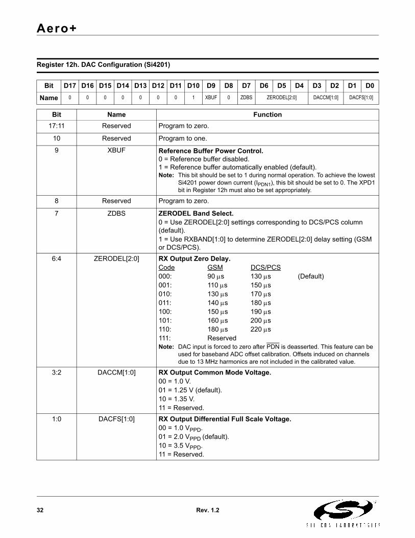
Register 12h. DAC Configuration (Si4201)
Bit D17 D16 D15 D14 D13 D12 D11 D10 D9 D8 D7 D6 D5 D4 D3 D2 D1 D0
Name 0 0 0 0 0 0 0 1 XBUF 0 ZDBS ZERODEL[2:0] DACCM[1:0] DACFS[1:0]
Bit Name Function17:11 Reserved Program to zero.
10 Reserved Program to one.
9 XBUF Reference Buffer Power Control.0 = Reference buffer disabled.1 = Reference buffer automatically enabled (default).Note: This bit should be set to 1 during normal operation. To achieve the lowest
Si4201 power down current (IPDN1), this bit should be set to 0. The XPD1 bit in Register 12h must also be set appropriately.
8 Reserved Program to zero.
7 ZDBS ZERODEL Band Select.0 = Use ZERODEL[2:0] settings corresponding to DCS/PCS column (default).1 = Use RXBAND[1:0] to determine ZERODEL[2:0] delay setting (GSM or DCS/PCS).
6:4 ZERODEL[2:0] RX Output Zero Delay.Code GSM DCS/PCS000: 90 µs 130 µs (Default)001: 110 µs 150 µs010: 130 µs 170 µs011: 140 µs 180 µs100: 150 µs 190 µs101: 160 µs 200 µs110: 180 µs 220 µs111: ReservedNote: DAC input is forced to zero after PDN is deasserted. This feature can be
used for baseband ADC offset calibration. Offsets induced on channels due to 13 MHz harmonics are not included in the calibrated value.
3:2 DACCM[1:0] RX Output Common Mode Voltage.00 = 1.0 V.01 = 1.25 V (default).10 = 1.35 V.11 = Reserved.
1:0 DACFS[1:0] RX Output Differential Full Scale Voltage.00 = 1.0 VPPD.01 = 2.0 VPPD (default).10 = 3.5 VPPD.11 = Reserved.

Aero+
Rev. 1.2 33
Notes:1. See registers 03h and 33h for bit definitions.2. When this register is written, the PDIB bit automatically sets to 0, the PDRB bit is set to 1, and the RFUP bit is set as a
function of RXBAND[1:0].
Note: See registers 05h and 11h for bit definitions.
Notes:1. See register 05h for bit definitions.2. The DGAIN[5:0] in Register 22h can be changed without powering down.
Notes:1. See registers 03h and 34h for bit definitions.2. When this register is written, the PDIB bit automatically sets to 1, and the PDRB bit is set to 1.
Register 19h. Reserved (Si4201)
Bit D17 D16 D15 D14 D13 D12 D11 D10 D9 D8 D7 D6 D5 D4 D3 D2 D1 D0
Name 0 0 0 0 0 0 0 0 0 0 0 0 0 0 0 0 0 0
Bit Name Function17:0 Reserved Program to zero.
Register 20h. RX Master #1
Bit D17 D16 D15 D14 D13 D12 D11 D10 D9 D8 D7 D6 D5 D4 D3 D2 D1 D0
Name RXBAND[1:0] NRF1[15:0]
Register 21h. RX Master #2
Bit D17 D16 D15 D14 D13 D12 D11 D10 D9 D8 D7 D6 D5 D4 D3 D2 D1 D0
Name 0 DPDS[2:0] LNAC[1:0] LNAG[1:0] AGAIN[2:0] 0 DGAIN[5:0]
Register 22h. RX Master #3
Bit D17 D16 D15 D14 D13 D12 D11 D10 D9 D8 D7 D6 D5 D4 D3 D2 D1 D0
Name 0 0 0 0 0 0 0 0 0 0 0 0 DGAIN[5:0]
Register 23h. TX Master #1
Bit D17 D16 D15 D14 D13 D12 D11 D10 D9 D8 D7 D6 D5 D4 D3 D2 D1 D0
Name TXBAND[1:0] NRF2[15:0]

Aero+
34 Rev. 1.2
Note: See registers 04h and 35h for bit definitions.
Note: Registers on the Si4134T can be read by writing this register with the address of the register to be read.
Register 24h. TX Master #2
Bit D17 D16 D15 D14 D13 D12 D11 D10 D9 D8 D7 D6 D5 D4 D3 D2 D1 D0
Name FIF[3:0] NIF[13:0]
Register 28h. CDAC (Si4134T)
Bit D17 D16 D15 D14 D13 D12 D11 D10 D9 D8 D7 D6 D5 D4 D3 D2 D1 D0
Name 0 0 0 0 0 0 0 0 0 0 0 0 CDAC[5:0]
Bit Name Function17:6 Reserved Read as zero.
5:0 CDAC[5:0] DCXO Coarse Frequency DAC Adjustment.64 steps. See Table 8 on page 15 for step size. An increase in CDAC results in a lower oscillating frequency. Likewise, a decrease in CDAC results in a higher oscillating frequency.000000 = Highest frequency...111111 = Lowest frequency
Register 30h. Revision/Read (Si4134T)
Bit D17 D16 D15 D14 D13 D12 D11 D10 D9 D8 D7 D6 D5 D4 D3 D2 D1 D0
Name 0 0 0 0 0 0 0 0 0 0 REV3[7:0]
Bit Name Function17:8 Reserved Read as zero.
7:0 REV3[7:0] Si4134T Revision (read only).C0h = Rev A (latest version).

Aero+
Rev. 1.2 35
Register 31h. Main Configuration (Si4134T)
Bit D17 D16 D15 D14 D13 D12 D11 D10 D9 D8 D7 D6 D5 D4 D3 D2 D1 D0
Name 0 0 0 SDOSEL[3:0] 0 0 0 0 0 0 RFUP DIV2 0 0 0
Bit Name Function17:15 Reserved Program to zero.
14:11 SDOSEL[3:0] SDO Output Control Register.The mux_output table is as follows:
0000 Connected to the Output Shift Register (default).0001 Force the Output to Low.0010 Reference Clock.0011 Lock Detect (LDETB) Signal from Phase Detectors.1111 High Impedance.
Notes:1. SDO is high-impedance when PDN = 0.2. SDO is Serial Data Output when in register read mode.
10:5 Reserved Program to zero.
4 RFUP RF PLL Update Rate (RF1 VCO only).0 = 200 kHz update rate (Receive GSM modes).1 = 100 kHz update rate (Receive DCS and PCS modes).Note: This bit is set to 1 when Register 20h D[17:16] = 01b or 10b (DCS 1800 or
PCS 1900 receive modes) and is set to 0 when D[17:16] = 00b or 11b (GSM 850 or GSM 900 modes).
3 DIV2 Input Clock Frequency.0 = No divider. XIN = 13 MHz.1 = Divide XIN by 2. XIN = 26 MHz.
2:0 Reserved Program to zero.

Aero+
36 Rev. 1.2
Register 32h. Powerdown (Si4134T)
Bit D17 D16 D15 D14 D13 D12 D11 D10 D9 D8 D7 D6 D5 D4 D3 D2 D1 D0
Name 0 0 0 0 0 0 0 0 0 0 0 0 0 0 0 0 PDIB PDRB
Bit Name Function17:2 Reserved Program to zero.
1 PDIB Powerdown IF PLL.0 = IF synthesizer powered down.1 = IF synthesizer powered up when the PDN pin is high.Notes:
1. The IF PLL is only used in transmit mode. Powerdown for receive mode. 2. This bit is set to 0 when register 20h is written (receive mode).3. This bit is set to 1 when register 23h is written (transmit mode).
0 PDRB Powerdown RF PLL.0 = RF synthesizer powered down.1 = RF synthesizer powered up when the PDN pin is high.Notes:
1. This bit is set to 1 when register 20h is written (receive mode).2. This bit is set to 1 when register 23h is written (transmit mode).
Register 33h. RF1 N Divider (Si4134T)
Bit D17 D16 D15 D14 D13 D12 D11 D10 D9 D8 D7 D6 D5 D4 D3 D2 D1 D0
Name 0 0 NRF1[15:0]
Bit Name Function17:16 Reserved Program to zero.15:0 NRF1[15:0] N Divider for RF PLL (RF1 VCO).
Used for Receive mode.
Register 34h. RF2 N Divider (Si4134T)
Bit D17 D16 D15 D14 D13 D12 D11 D10 D9 D8 D7 D6 D5 D4 D3 D2 D1 D0
Name 0 0 NRF2[15:0]
Bit Name Function17:16 Reserved Program to zero.15:0 NRF2[15:0] N Divider for RF PLL (RF2 VCO).
Used for Transmit mode.

Aero+
Rev. 1.2 37
Register 35h. IF N Divider (Si4134T)
Bit D17 D16 D15 D14 D13 D12 D11 D10 D9 D8 D7 D6 D5 D4 D3 D2 D1 D0
Name 0 0 NIF[15:0]
Bit Name Function17:16 Reserved Program to zero.15:0 NIF[15:0] N Divider for IF Synthesizer.
Used for transmit mode.
Aero+
38 Rev. 1.2
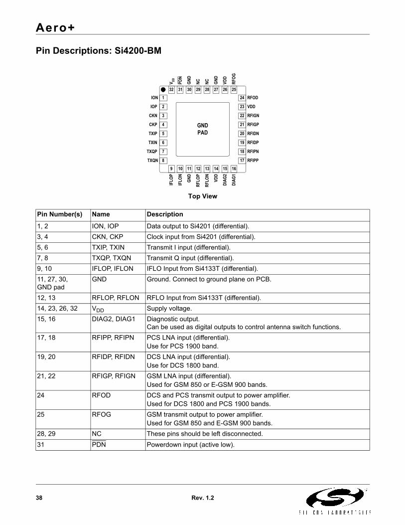
Pin Descriptions: Si4200-BM
Pin Number(s) Name Description
1, 2 ION, IOP Data output to Si4201 (differential).3, 4 CKN, CKP Clock input from Si4201 (differential).5, 6 TXIP, TXIN Transmit I input (differential).7, 8 TXQP, TXQN Transmit Q input (differential).9, 10 IFLOP, IFLON IFLO Input from Si4133T (differential).11, 27, 30, GND pad
GND Ground. Connect to ground plane on PCB.
12, 13 RFLOP, RFLON RFLO Input from Si4133T (differential).14, 23, 26, 32 VDD Supply voltage.15, 16 DIAG2, DIAG1 Diagnostic output.
Can be used as digital outputs to control antenna switch functions.17, 18 RFIPP, RFIPN PCS LNA input (differential).
Use for PCS 1900 band.19, 20 RFIDP, RFIDN DCS LNA input (differential).
Use for DCS 1800 band.21, 22 RFIGP, RFIGN GSM LNA input (differential).
Used for GSM 850 or E-GSM 900 bands.24 RFOD DCS and PCS transmit output to power amplifier.
Used for DCS 1800 and PCS 1900 bands.25 RFOG GSM transmit output to power amplifier.
Used for GSM 850 and E-GSM 900 bands.28, 29 NC These pins should be left disconnected.31 PDN Powerdown input (active low).
Top View
GNDPAD
1
2
3
2526272829303132ION
IOP
TXQN
TXQP
CKN
CKP
TXIN
TXIP
IFLO
P
IFLO
N
GND
RFLO
P
RFLO
N
VDD
DIAG
2
DIAG
1
V DD PDN
GND
NC NC GND
VDD
RFOG
RFIDP
RFIDN
RFIPP
RFIPN
RFIGP
RFIGN
VDD
RFOD
17
18
19
20
21
22
23
24
9 10 11 12 13 14 15 16
4
5
6
7
8
Aero+
Rev. 1.2 39
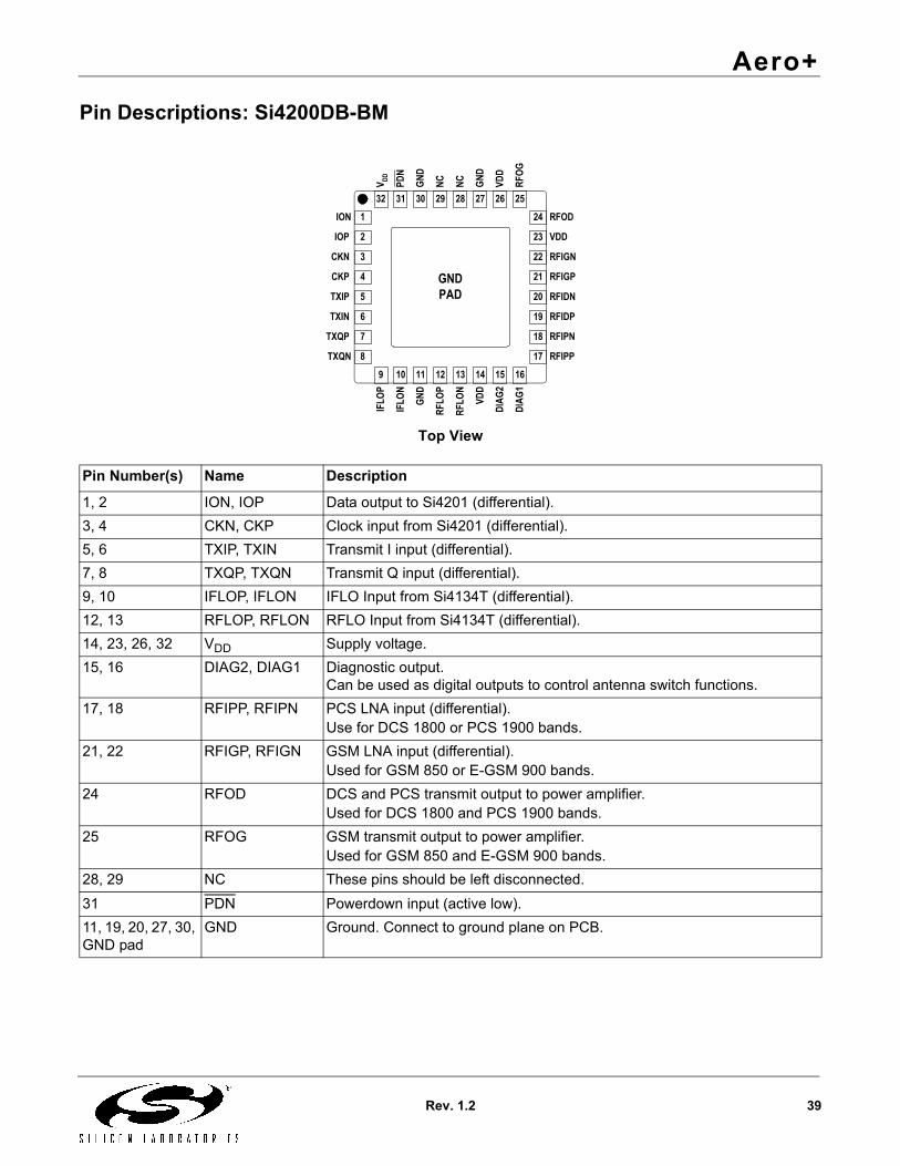
Pin Descriptions: Si4200DB-BM
Pin Number(s) Name Description
1, 2 ION, IOP Data output to Si4201 (differential).3, 4 CKN, CKP Clock input from Si4201 (differential).5, 6 TXIP, TXIN Transmit I input (differential).7, 8 TXQP, TXQN Transmit Q input (differential).9, 10 IFLOP, IFLON IFLO Input from Si4134T (differential).12, 13 RFLOP, RFLON RFLO Input from Si4134T (differential).14, 23, 26, 32 VDD Supply voltage.15, 16 DIAG2, DIAG1 Diagnostic output.
Can be used as digital outputs to control antenna switch functions.17, 18 RFIPP, RFIPN PCS LNA input (differential).
Use for DCS 1800 or PCS 1900 bands.21, 22 RFIGP, RFIGN GSM LNA input (differential).
Used for GSM 850 or E-GSM 900 bands.24 RFOD DCS and PCS transmit output to power amplifier.
Used for DCS 1800 and PCS 1900 bands.25 RFOG GSM transmit output to power amplifier.
Used for GSM 850 and E-GSM 900 bands.28, 29 NC These pins should be left disconnected.31 PDN Powerdown input (active low).11, 19, 20, 27, 30, GND pad
GND Ground. Connect to ground plane on PCB.
Top View
GNDPAD
1
2
3
2526272829303132ION
IOP
TXQN
TXQP
CKN
CKP
TXIN
TXIP
IFLO
P
IFLO
N
GND
RFLO
P
RFLO
N
VDD
DIAG
2
DIAG
1
V DD PDN
GND
NC NC GND
VDD
RFOG
RFIDP
RFIDN
RFIPP
RFIPN
RFIGP
RFIGN
VDD
RFOD
17
18
19
20
21
22
23
24
9 10 11 12 13 14 15 16
4
5
6
7
8

Aero+
40 Rev. 1.2
Pin Descriptions: Si4201-BM
Pin Number(s) Name Description
2, 3 RXQP, RXQN Receive Q output (differential).4, 5 RXIP, RXIN Receive I output (differential).6, 20 VDD Supply voltage.7 XIN Reference frequency input from crystal oscillator.9, 10 CKP, CKN Clock output to Si4200 (differential).11, 12 IOP, ION Data input from Si4200 (differential).13 XEN XOUT pin enable14 PDN Powerdown input (active low).15 SDO Serial data output.16 SEN Serial enable input (active low).17 SCLK Serial clock input.18 SDI Serial data input.19 XOUT Clock output to baseband.1, 8, GND pad
GND Ground. Connect to ground plane on PCB.
Top View
GNDPAD
1
2
3
1617181920GND
RXQP
RXQN
RXIP
RXIN
VDD
XIN
GND
CKP
CKN
V DD XOUT
SDI
SCLK
SEN
IOP
ION
XEN
PDN
SDO
11
12
13
14
15
6 7 8 9 10
4
5
Aero+
Rev. 1.2 41
Pin Descriptions: Si4134T-BM
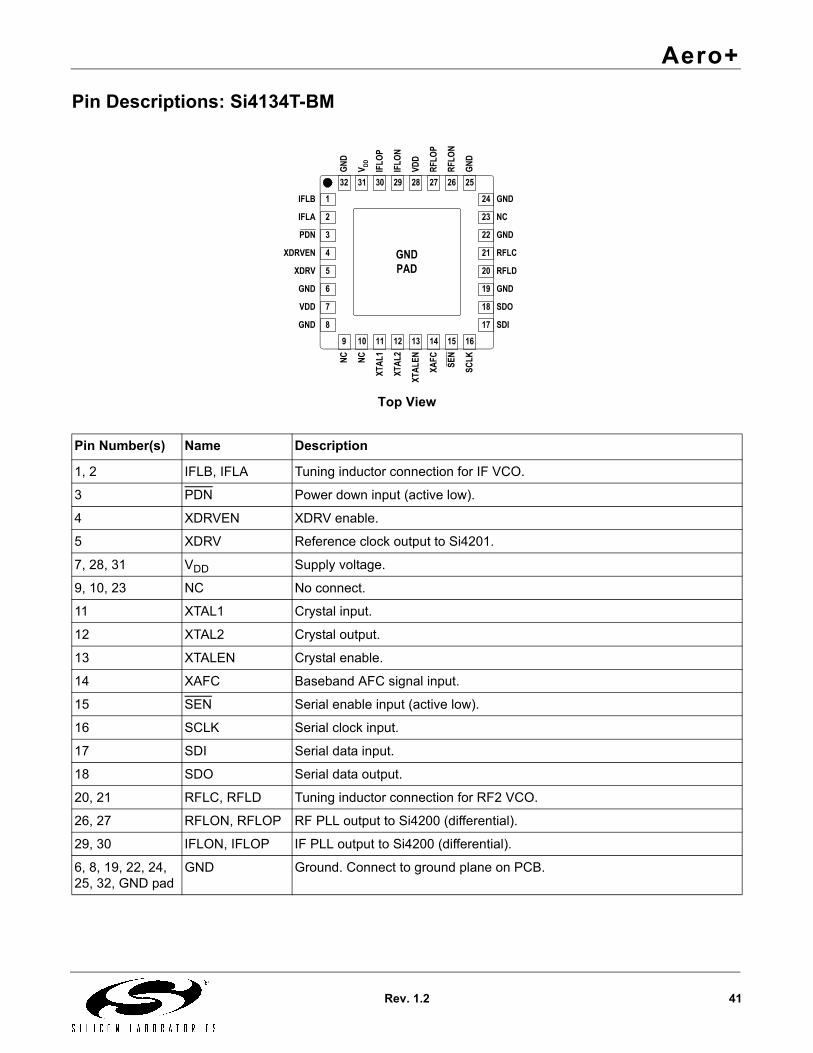
Pin Number(s) Name Description
1, 2 IFLB, IFLA Tuning inductor connection for IF VCO.
3 PDN Power down input (active low).
4 XDRVEN XDRV enable.
5 XDRV Reference clock output to Si4201.
7, 28, 31 VDD Supply voltage.
9, 10, 23 NC No connect.
11 XTAL1 Crystal input.
12 XTAL2 Crystal output.
13 XTALEN Crystal enable.
14 XAFC Baseband AFC signal input.
15 SEN Serial enable input (active low).
16 SCLK Serial clock input.
17 SDI Serial data input.
18 SDO Serial data output.
20, 21 RFLC, RFLD Tuning inductor connection for RF2 VCO.
26, 27 RFLON, RFLOP RF PLL output to Si4200 (differential).
29, 30 IFLON, IFLOP IF PLL output to Si4200 (differential).
6, 8, 19, 22, 24, 25, 32, GND pad
GND Ground. Connect to ground plane on PCB.
Top View
GNDPAD
1
2
3
2526272829303132IFLB
IFLA
GND
VDD
PDN
XDRVEN
GND
XDRV
NC NC
XTAL
1
XTAL
2
XTAL
EN
XAFC SE
N
SCLK
GND
V DD IFLO
P
IFLO
N
VDD
RFLO
P
RFLO
N
GND
GND
RFLD
SDI
SDO
RFLC
GND
NC
GND
17
18
19
20
21
22
23
24
9 10 11 12 13 14 15 16
4
5
6
7
8
Aero+
42 Rev. 1.2
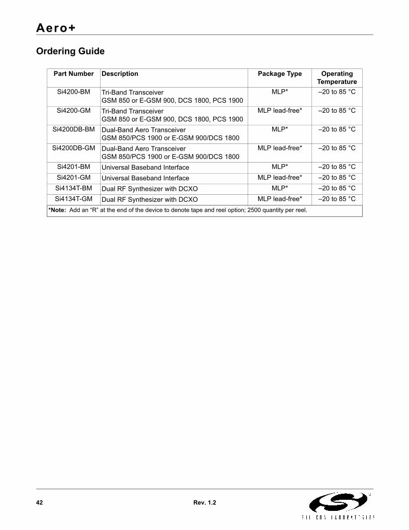
Ordering Guide
Part Number Description Package Type Operating Temperature
Si4200-BM Tri-Band TransceiverGSM 850 or E-GSM 900, DCS 1800, PCS 1900
MLP* –20 to 85 °C
Si4200-GM Tri-Band TransceiverGSM 850 or E-GSM 900, DCS 1800, PCS 1900
MLP lead-free* –20 to 85 °C
Si4200DB-BM Dual-Band Aero TransceiverGSM 850/PCS 1900 or E-GSM 900/DCS 1800
MLP* –20 to 85 °C
Si4200DB-GM Dual-Band Aero TransceiverGSM 850/PCS 1900 or E-GSM 900/DCS 1800
MLP lead-free* –20 to 85 °C
Si4201-BM Universal Baseband Interface MLP* –20 to 85 °CSi4201-GM Universal Baseband Interface MLP lead-free* –20 to 85 °CSi4134T-BM Dual RF Synthesizer with DCXO MLP* –20 to 85 °CSi4134T-GM Dual RF Synthesizer with DCXO MLP lead-free* –20 to 85 °C
*Note: Add an “R” at the end of the device to denote tape and reel option; 2500 quantity per reel.

Aero+
Rev. 1.2 43
Package Outline: Si4200-BM and Si4200DB-BMFigure 18 illustrates the package details for the Si4200-BM and Si4200DB-BM. Table 12 lists the values for thedimensions shown in the illustration.
Figure 18. 32-Pin Micro Leadframe Package (MLP)
Table 12. Package Dimensions
Symbol Millimeters Symbol MillimetersMin Nom Max Min Nom Max
A — 0.85 0.90 D1, E1 4.75 BSC
A1 0.00 0.01 0.05 D2, E2 3.15 3.30 3.45
A2 — 0.65 0.70 e 0.50 BSC
A3 0.20 REF. θ — — 12°
b 0.18 0.23 0.30 L 0.30 0.40 0.50
D, E 5.00 BSCNotes:
1. Dimensioning and tolerances conform to ASME Y14.5M. - 19942. Package warpage MAX 0.05 mm.3. “b” applies to plated terminal and is measured between 0.20 and 0.25 mm from terminal TIP.4. The package weight is approximately 68 mg.5. The mold compound for this package has a flammability rating of UL94-V0 with an oxygen index of 28
minimum/54 typical.6. The recommended reflow profile for this package is defined by the JEDEC-020B Small Body specification.
32
Bottom View
11
E2
D2
23
Top View Side View
A
A1
A2
A3
θ
23
PIN1 ID0.50 DIA.
b
32
b
e
L PIN1 ID0.20 R.
e
EE1
D
D1
Aero+
44 Rev. 1.2
Package Outline: Si4201-BMFigure 19 illustrates the package details for the Si4201-BM. Table 13 lists the values for the dimensions shown inthe illustration.
Figure 19. 20-Pin Micro Leadframe Package (MLP)
Table 13. Package Dimensions
Symbol Millimeters Symbol Millimeters
Min Nom Max Min Nom MaxA — 0.85 0.90 D1, E1 3.75 BSC
A1 0.00 0.01 0.05 D2, E2 1.95 2.10 2.25
A2 — 0.65 0.70 e 0.50 BSC
A3 0.20 REF. θ — — 12°
b 0.18 0.23 0.30 L 0.50 0.60 0.75
D, E 4.00 BSC
Notes:1. Dimensioning and tolerances conform to ASME Y14.5M. - 19942. Package warpage MAX 0.05 mm.3. “b” applies to plated terminal and is measured between 0.20 and 0.25 mm from terminal TIP.4. The package weight is approximately 42 mg.5. The mold compound for this package has a flammability rating of UL94-V0 with an oxygen index of 28
minimum/54 typical.6. The recommended reflow profile for this package is defined by the JEDEC-020B Small Body specification.
20
Bottom View
11
E2
D2
23
Top View Side View
A
A1
A2
A3
θ
23 EE1
PIN1 ID0.50 DIA.
D
b20
D1
b
ee
L
Aero+
Rev. 1.2 45
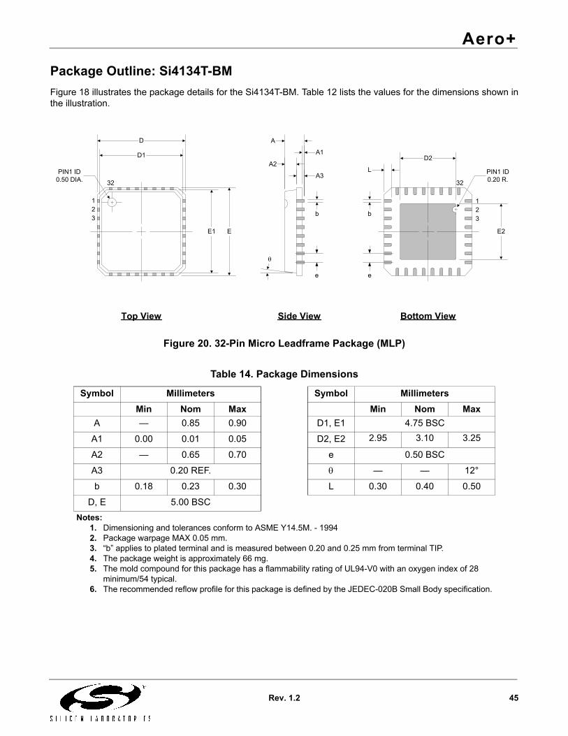
Package Outline: Si4134T-BMFigure 18 illustrates the package details for the Si4134T-BM. Table 12 lists the values for the dimensions shown inthe illustration.
Figure 20. 32-Pin Micro Leadframe Package (MLP)
Table 14. Package Dimensions
Symbol Millimeters Symbol MillimetersMin Nom Max Min Nom Max
A — 0.85 0.90 D1, E1 4.75 BSC
A1 0.00 0.01 0.05 D2, E2 2.95 3.10 3.25
A2 — 0.65 0.70 e 0.50 BSC
A3 0.20 REF. θ — — 12°
b 0.18 0.23 0.30 L 0.30 0.40 0.50
D, E 5.00 BSCNotes:
1. Dimensioning and tolerances conform to ASME Y14.5M. - 19942. Package warpage MAX 0.05 mm.3. “b” applies to plated terminal and is measured between 0.20 and 0.25 mm from terminal TIP.4. The package weight is approximately 66 mg.5. The mold compound for this package has a flammability rating of UL94-V0 with an oxygen index of 28
minimum/54 typical.6. The recommended reflow profile for this package is defined by the JEDEC-020B Small Body specification.
32
Bottom View
11
E2
D2
23
Top View Side View
A
A1
A2
A3
θ
23
PIN1 ID0.50 DIA.
b
32
b
e
L PIN1 ID0.20 R.
e
EE1
D
D1

Aero+
46 Rev. 1.2
Document Change ListRevision 1.0 to Revision 1.1
This document corresponds to the following:Si4200DB revision E (dual band LNA) or Si4200 revision F (triple band LNA)Si4201 revision CSi4134T revision A
"Bill of Materials" on page 17Updated L1–-L3 with 0402 sizes.
"Ordering Guide" on page 42 updated to include lead-free ordering option."Package Outline: Si4200-BM and Si4200DB-BM" on page 43 (documentation change only, no change to part)
Updated D2,E2 dimensions.Updated device weight.Added notes 5 and 6.
"Package Outline: Si4201-BM" on page 44 (documentation change only, no change to part)
Updated L dimension.Updated device weight.Added notes 5 and 6.
"Package Outline: Si4134T-BM" on page 45 (documentation change only, no change to part)
Updated L dimension.Updated device weight.Added notes 5 and 6.
Revision 1.1 to Revision 1.2This document corresponds to the following:
Si4200DB revision E (dual band LNA) or Si4200 revision F (triple band LNA)Si4201 revision CSi4134T revision A
"Package Outline: Si4134T-BM" on page 45 (documentation change only, no change to part)
Updated L dimension

Aero+
Rev. 1.2 47
Notes:

Aero+
48 Rev. 1.2
Contact InformationSilicon Laboratories Inc.4635 Boston LaneAustin, Texas 78735Tel:1+ (512) 416-8500Fax:1+ (512) 416-9669Toll Free:1+ (877) 444-3032Email: [email protected]: www.silabs.com
Silicon Laboratories, Silicon Labs, and Aero are trademarks of Silicon Laboratories Inc.Other products or brand names mentioned herein are trademarks or registered trademarks of their respective holder
The information in this document is believed to be accurate in all respects at the time of publication but is subject to change without notice. Silicon Laboratories assumes no responsibility for errors and omissions, and disclaims responsibility for any consequences resulting from the use of information included herein. Additionally, Silicon Laboratories assumes no responsibility for the functioning of undescribed fea-tures or parameters. Silicon Laboratories reserves the right to make changes without further notice. Silicon Laboratories makes no war-
ranty, representation or guarantee regarding the suitability of its products for any particular purpose, nor does Silicon Laboratories assume any liability arising out of the application or use of any product or circuit, and specifically disclaims any and all liability, including without
limitation consequential or incidental damages. Silicon Laboratories products are not designed, intended, or authorized for use in applica-tions intended to support or sustain life, or for any other application in which the failure of the Silicon Laboratories product could create a situation where personal injury or death may occur. Should Buyer purchase or use Silicon Laboratories products for any such unintended
or unauthorized application, Buyer shall indemnify and hold Silicon Laboratories harmless against all claims and damages.