Embed Size (px)
Citation preview
Aerogel Structures for Photocathodes
Michael PellinArgonne Distinguished FellowDirector, Materials Science Division
Thomas Prolier, Jeff Elam, Alex Martinson Stacey Standridge (NU), Joe Hupp (NU)
1st Workshop on Photo-cathodes: 300nm-500nmJuly 20-21, 2009: University of Chicago
Photocathode WorkshopJuly 20-21, 2009
University of Chicago
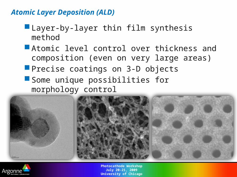
Atomic Layer Deposition (ALD)
Layer-by-layer thin film synthesis method Atomic level control over thickness and composition
(even on very large areas) Precise coatings on 3-D objects Some unique possibilities for morphology control
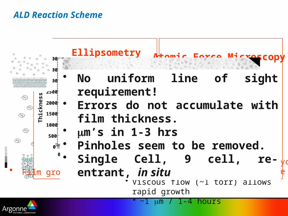
ALD Reaction Scheme
• ALD involves the use of a pair of reagents.• each reacts with the surface completely• each will not react with itself
• This setup eliminates line of site requirments
• Application of this AB Scheme• Reforms the surface• Adds precisely 1 monolayer
• Pulsed Valves allow atomic layer precision in growth
• Viscous flow (~1 torr) allows rapid growth• ~1 mm / 1-4 hours
0
500
1000
1500
2000
2500
3000
3500
4000
0 500 1000 1500 2000 2500 3000AB Cycles
Th
ick
nes
s (Å
)
Ellipsometry Atomic Force Microscopy
• Film growth is linear with AB Cycles• RMS Roughness = 4 Å (3000 Cycles)• ALD Films Flat, Pinhole freeFlat, Pinhole-Free Film
Seagate, Stephen Ferro
• No uniform line of sight requirement!• Errors do not accumulate with film
thickness.• mm’s in 1-3 hrs• Pinholes seem to be removed.• Single Cell, 9 cell, re-entrant, in situ
Photocathode WorkshopJuly 20-21, 2009
University of Chicago
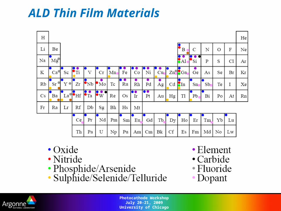
ALD Thin Film Materials
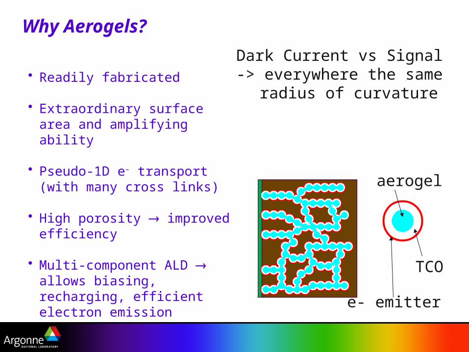
• Readily fabricated
• Extraordinary surface area and amplifying ability
• Pseudo-1D e- transport (with many cross links)
• High porosity improved efficiency
• Multi-component ALD allows biasing, recharging, efficient electron emission
e- emitter
aerogel
TCO
Why Aerogels?
Dark Current vs Signal-> everywhere the same
radius of curvature
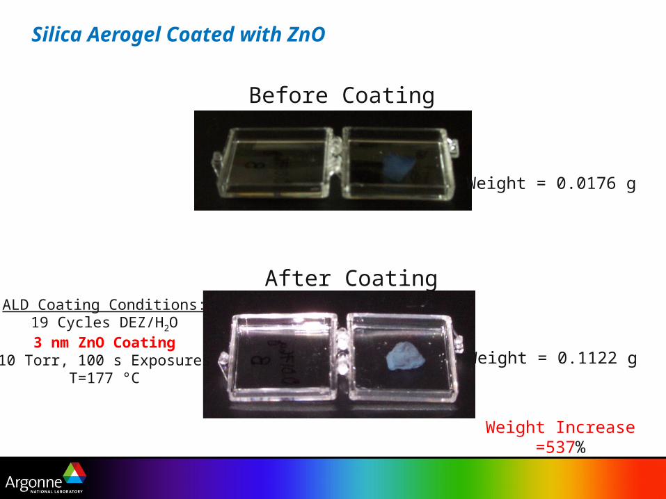
Before Coating
After Coating
Weight = 0.0176 g
Weight = 0.1122 g
Weight Increase=537%
ALD Coating Conditions:19 Cycles DEZ/H2O3 nm ZnO Coating
10 Torr, 100 s ExposuresT=177 °C
Silica Aerogel Coated with ZnO
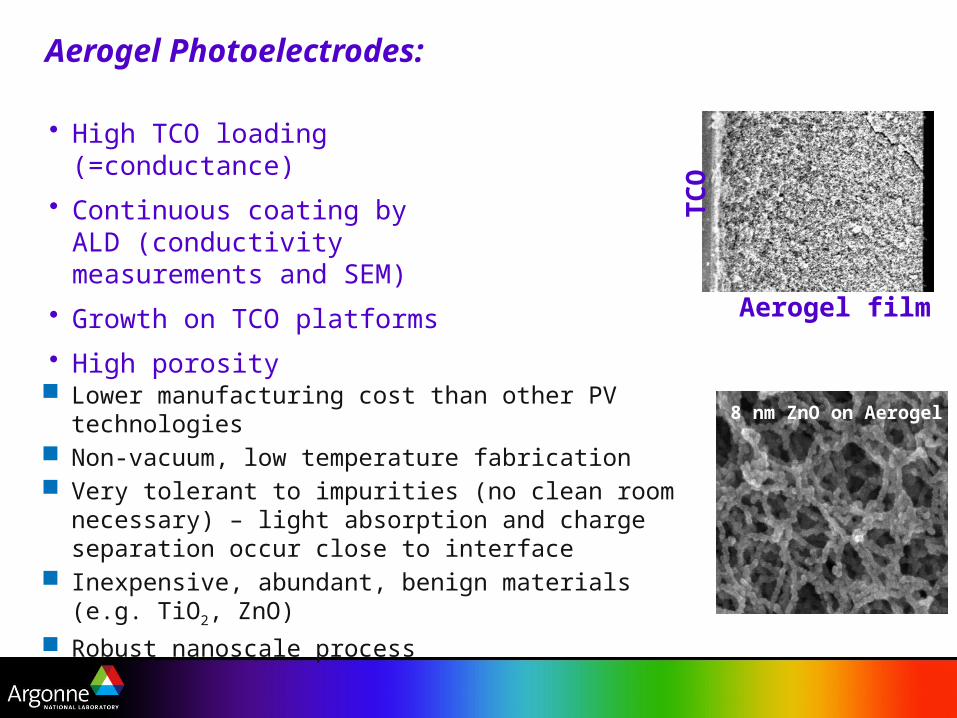
• High TCO loading (=conductance)
• Continuous coating by ALD (conductivity measurements and SEM)
• Growth on TCO platforms
• High porosity
Aerogel film
TC
O
8 nm ZnO on Aerogel
Aerogel Photoelectrodes:
Lower manufacturing cost than other PV technologies Non-vacuum, low temperature fabrication Very tolerant to impurities (no clean room necessary) –
light absorption and charge separation occur close to interface
Inexpensive, abundant, benign materials (e.g. TiO2, ZnO)
Robust nanoscale process
Photocathode WorkshopJuly 20-21, 2009
University of Chicago
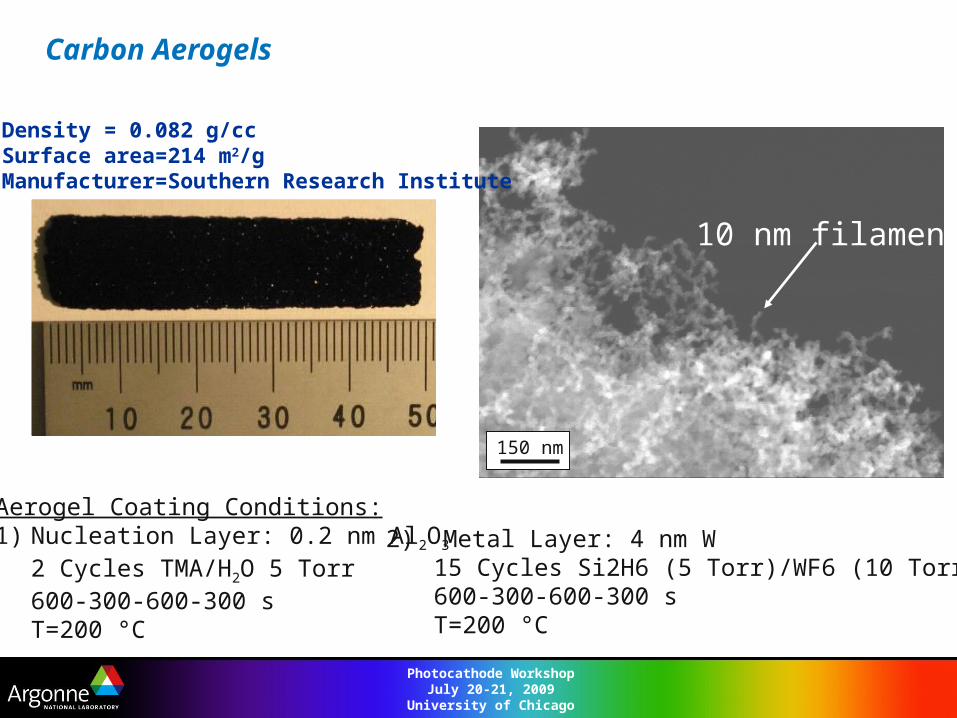
Density = 0.082 g/ccSurface area=214 m2/gManufacturer=Southern Research Institute
10 nm filaments
150 nm
Aerogel Coating Conditions:1) Nucleation Layer: 0.2 nm Al2O3
2 Cycles TMA/H2O 5 Torr600-300-600-300 sT=200 °C
Carbon Aerogels
2) Metal Layer: 4 nm W15 Cycles Si2H6 (5 Torr)/WF6 (10 Torr)600-300-600-300 sT=200 °C
Photocathode WorkshopJuly 20-21, 2009
University of Chicago
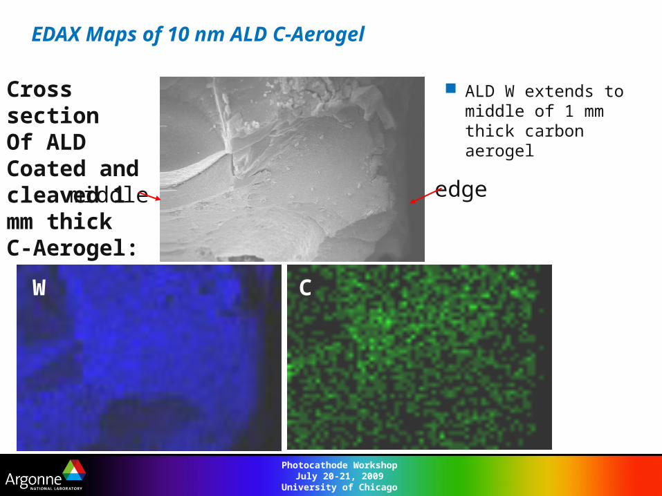
EDAX Maps of 10 nm ALD C-Aerogel
ALD W extends to middle of 1 mm thick carbon aerogel
edgemiddle
W C
Cross section Of ALD Coated and cleaved 1 mm thickC-Aerogel:
Photocathode WorkshopJuly 20-21, 2009
University of Chicago
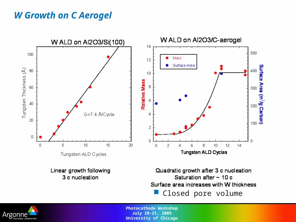
W Growth on C Aerogel
Closed pore volume
Photocathode WorkshopJuly 20-21, 2009
University of Chicago
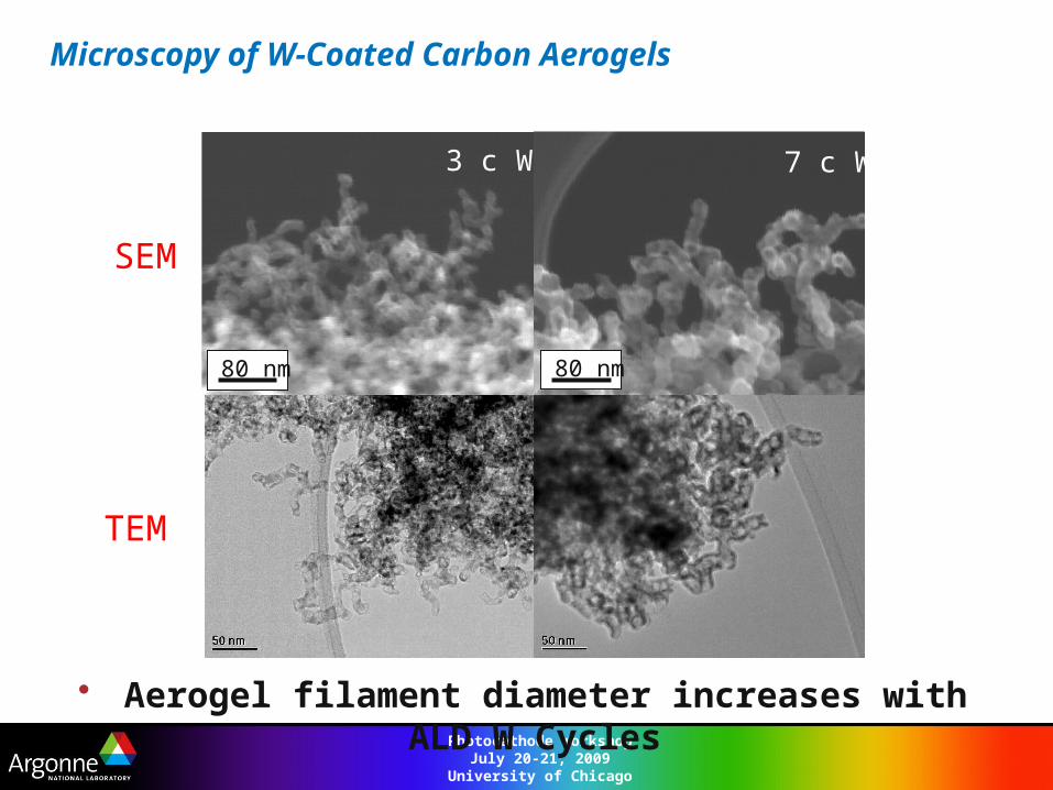
• Aerogel filament diameter increases with ALD W Cycles
SEM
TEM
80 nm
3 c W 7 c W
80 nm
Microscopy of W-Coated Carbon Aerogels
Photocathode WorkshopJuly 20-21, 2009
University of Chicago
Metal-coated aerogels are pyrophoric!
Photocathode WorkshopJuly 20-21, 2009
University of Chicago
Conclusions: Aerogels
Aerogels are one of many nanostructured materials that may be of interest to the detector community.
Aerogels can be coated allowing the resistivity necessary to provide a kilovolt gradient.
Abundant surface area means amplification should be achieved over relatively thin structures.
Large areas are relatively easy to achieve + the self limiting properties of ALD encourages one to believe that these large areas can be uniformly coated.
Interestingly– channel plate detectors achieve uniform flight times with very uniform
structures– Aerogels would achieve uniformity with random structure averaging
Remember 2ndary electrons are ejected without memory of their incoming direction.