Embed Size (px)
Citation preview
Avago Technologies Proprietary
• Real time monitoring of:- Transmitter average optical power- Received average optical power- Laser bias current- Temperature- Supply Voltage
• SFP28 mechanical specifications per SFF-8432• SFP28 compliant low speed interface per SFF-8419• Fibre Channel FC-PI-6 compliant high speed interface
- 3200-M5-SN-S, 1600-M5-SN-S, 800-M5-SN-S- 3200-M5E-SN-I, 1600-M5E-SN-I, 800-M5E-SN-I- 3200-M5F-SN-I, 1600-M5F-SN-I, 800-M5F-SN-I
• Fibre Channel FC-PI-6 compliant optical link distances
Applications• Fibre Channel switches (director, stand alone, blade)• Fibre Channel Host Bus Adapters• Fibre Channel RAID controllers• Fibre Channel tape drive• Port side connections• Inter-switch or inter-chassis aggregated links
DescriptionAvago Technologies’ AFBR-57G5MZ optical transceiver supports high speed serial links over multi-mode optical fiber at signalling rates up to 28.05Gb/s (the serial line rate of 32GFC). The product is compliant with Small Form Plug-gable industry agreements SFP and SFP28 for mechanical and low speed electrical specifications. High speed elec-trical and optical specifications are compliant with ANSI Fibre Channel FC-PI-6.
The AFBR-57G5MZ is a multi-rate 850nm transceiver which ensures compliance with FC-PI-6 32GFC, 16GFC and 8GFC specifications. Per the requirements of 32GFC, inter-nal clock and data recovery circuits (CDRs) are present on both electrical input and electrical output of this trans-ceiver. These CDRs will lock at 28.05Gb/s and 14.025Gb/s (32GFC and 16GFC) but must be bypassed for operation at 8.5Gb/s (8GFC), accomplished by using two Rate Select inputs to configure transmit and receive sides. Transmitter and receiver can operate at different data rates, as is often seen during Fibre Channel speed negotiation.
Digital diagnostic monitoring information (DMI) is present in the AFBR-57G5MZ per the requirements of SFF-8472, providing real time monitoring information of transceiver laser, receiver and environment conditions over a SFF-8419 2-wire serial interface.
Related Products• AFCT-57G5MZ: 1310nm SFP for 32G/16G/8G Fibre Channel
• AFBR-57F5MZ: 850nm SFP for 16G/8G/4G Fibre Channel
• AFCT-57F5AMZ: 1310nm SFP for 16G/8G/4G Fibre Channel
• AFBR-57D9AMZ: 850nm SFP for 8G/4G/2G Fibre Channel
• AFCT-57D5ATPZ: 1310nm SFP for 8G/4G/2G Fibre Channel
• AFCT-57D5ANPZ: 1310nm SFP for 8G/4G/2G Fibre Channel
• AFBR-57R5APZ: 850nm SFP for 4G/2G/1G Fibre Channel
• AFCT-57R5APZ: 1310nm SFP for 4G/2G/1G Fibre Channel
• AFCT-57R5ATPZ: 1310nm SFP for 4G/2G/1G Fibre Channel
• AFCT-57R5ANPZ: 1310nm SFP for 4G/2G/1G Fibre ChannelPatent - www.avagotech.com/patents
Features• Compliant to RoHS directives• 850nm Vertical Cavity Surface Emitting Laser (VCSEL)• Class 1 eye safe per IEC60825-1 and CDRH• Wide temperature range (0°C to 70°C)• LC duplex connector optical interface conforming to
ANSI TIA/EIA604-10 (FOCIS 10A)• Diagnostic features per SFF-8472 “Diagnostic
Monitoring Interface for Optical Transceivers”
AFBR-57G5MZ32GFC SFP28 for Multi-Mode Optical FiberDigital Diagnostic SFP, 850nm, 32G/16G/8G Low Voltage (3.3V) Fibre Channel Optical Transceiver
Data Sheet
Avago Technologies Proprietary 2
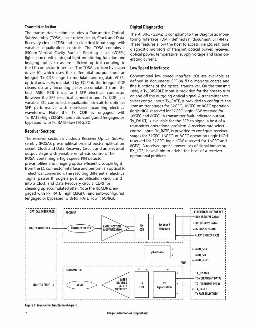
Figure 1. Transceiver functional diagram.
Rx Vout &Emphasis
RxCDR
TxEqualization
TxCDR
LIGHT FROM FIBER
LIGHT TO FIBER
PHOTO-DETECTOR
RECEIVER
AMPLIFICATION& QUANTIZATION
RD+ (RECEIVE DATA)
RD- (RECEIVE DATA)
Rx LOSS OF SIGNAL
VCSEL
TRANSMITTER
LASERDRIVER &
SAFETYCIRCUITRY
TX_DISABLE
TD+ (TRANSMIT DATA)
TD- (TRANSMIT DATA)
TX_FAULT
ELECTRICAL INTERFACE
MOD_SDA
MOD_SCLMOD_ABS
µController
OPTICAL INTERFACE
Rx RATE SELECT RS(0)
Tx RATE SELECT RS(1)
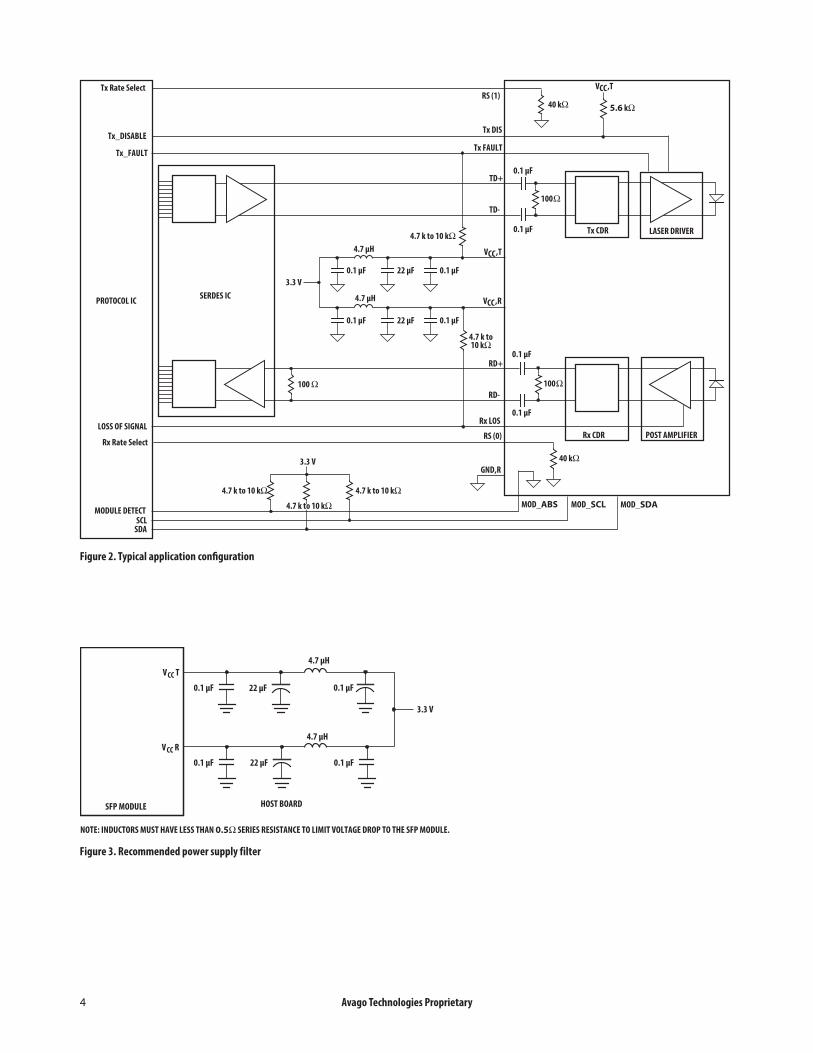
Transmitter SectionThe transmitter section includes a Transmitter Optical SubAssembly (TOSA), laser driver circuit, Clock and Data Recovery circuit (CDR) and an electrical input stage with variable equalization controls. The TOSA contains a 850nm Vertical Cavity Surface Emitting Laser (VCSEL) light source with integral light monitoring function and imaging optics to assure efficient optical coupling to the LC connector in-terface. The TOSA is driven by a laser driver IC, which uses the differential output from an integral Tx CDR stage to modulate and regulate VCSEL optical power. As mandated by FC-PI-6, the integral CDR cleans up any incoming jit-ter accumulated from the host ASIC, PCB traces and SFP electrical connector. Between the SFP electrical connector and Tx CDR is a variable, i2c controlled, equalization cir-cuit to optimize SFP performance with non-ideal incom-ing electrical waveforms. Note the Tx CDR is engaged with Tx_RATE=high (32GFC) and auto-configured (engaged or bypassed) with Tx_RATE=low (16G/8G).
Receiver Section:The receiver section includes a Receiver Optical SubAs-sembly (ROSA), pre-amplification and post-amplification circuit, Clock and Data Recovery Circuit and an electrical output stage with variable emphasis controls. The ROSA, containing a high speed PIN detector, pre-amplifier and imaging optics efficiently couple light from the LC connector interface and perform an optical to
electrical conversion. The resulting differential electrical signal passes through a post amplification circuit and into a Clock and Data Recovery circuit (CDR) for cleaning up accumulated jitter. Note the Rx CDR is en-gaged with Rx_RATE=high (32GFC) and auto-configured (engaged or bypassed) with Rx_RATE=low (16G/8G).
Digital Diagnostics:The AFBR-57G5MZ is compliant to the Diagnostic Moni-toring Interface (DMI) defined i n document SFF-8472. These features allow the host to access, via i2c, real time diagnostic monitors of transmit optical power, received optical power, temperature, supply voltage and laser op-erating current.
Low Speed Interfaces:
Conventional low speed interface I/Os are available as defined in documents SFF-8419 t o manage coarse and fine functions of the optical transceiver. On the transmit side, a Tx_DISABLE input is provided for the host to turn on and off the outgoing optical signal. A transmitter rate select control input, Tx_RATE, is provided to configure the transmitter stages for 32GFC, 16GFC or 8GFC operation (logic HIGH reserved for 32GFC, logic LOW reserved for 16GFC and 8GFC). A transmitter fault indicator output, Tx_FAULT, is available for the SFP to signal a host of a transmitter operational problem. A receiver rate select control input, Rx_RATE, is provided to configure receiver stages for 32GFC, 16GFC, or 8GFC operation (logic HIGH reserved for 32GFC, logic LOW reserved for 16GFC and 8GFC). A received optical power loss of signal indicator, RX_LOS, is available to advise the host of a receiver operational problem.
Avago Technologies Proprietary 3
Table 1. Regulatory Compliance
Feature Test Method PerformanceElectrostatic Discharge (ESD)to the Electrical Contacts
JEDEC Human Body Model (HBM)(JESD22-A114-B)
High speed contacts shall withstand 1000V. All other contacts shall withstand 2000 V.
Electrostatic Discharge (ESD) to the Optical Connector Receptacle
EN61000-4-2, Criterion B When installed in a properly grounded housing and chassis the units are subject-ed to 15kV air discharges during operation and 8kV direct discharges to the case.
Electromagnetic Interference (EMI) FCC Part 15 CENELEC EN55022(CISPR 22A) VCCI Class 1
System margins are dependent on cus-tomer board and chassis design.
Immunity Variation of IEC 61000-4-3 Typically shows no measurable effect from a 10V/m field swept from 80 MHz to 1 GHz applied to the module without a chassis enclosure
Laser Eye Safety and Equipment Type Testing
US FDA CDRH AEL Class 1US21 CFP, Subchapter J per Paragraphs 1002.10 and 1002.12
(IEC) EN60825-1:1994 +A11 +A2(IEC) EN60825-2:1994 +A1(IEC) EN60950:1992 +A1 +A2 +A3 +A4 +A11
CDRH Certification 9720151-155 TUV File: R72121699
Component Recognition Underwriters Laboratories (UL) and Canadian Standards Association (CSA) Joint Component Recognition for Information Technology Equip-ment including Electrical Business Equipment
UL File: E173874
RoHS Compliance Less than 1000 ppm of cadmium, lead, mercury, hexavalent chromium, polybro-minated biphenyls (PPB) and polybromi-nated biphenyl ethers (PBDE).
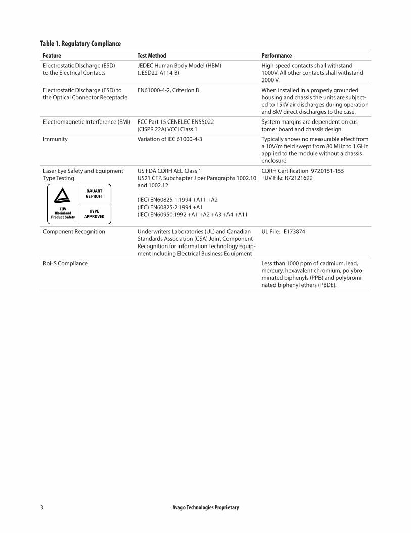
BAUARTGEPRUFT
TYPEAPPROVED
TUVRheinland
Product Safety
¬
¬
Avago Technologies Proprietary 4
Figure 2. Typical application configuration
4.7 µH
4.7 µH
0.1 µF
VCC R
SFP MODULE
22 µF
VCC T
0.1 µF
0.1 µF
3.3 V
HOST BOARD
0.1 µF
NOTE: INDUCTORS MUST HAVE LESS THAN 0.5Ω SERIES RESISTANCE TO LIMIT VOLTAGE DROP TO THE SFP MODULE.
Figure 3. Recommended power supply filter
22 µF
Tx CDR
MODULE DETECT
LOSS OF SIGNAL
SCLSDA
Tx_FAULT
Tx_DISABLE
TD+
Tx FAULT
Tx DIS
TD-
RD+
RD-
MOD_SDAMOD_SCLMOD_ABS
GND,R
4.7 k to10 kΩ
4.7 k to 10 kΩ4.7 k to 10 kΩ
PROTOCOL IC
VCC,T
VCC,T
VCC,R
4.7 µH
22 µF3.3 V
3.3 V
SERDES IC
Rx LOS
0.1 µF
Rx CDR
100 Ω
4.7 k to 10 kΩ
100 Ω
5.6 kΩ
4.7 k to 10 kΩ
LASER DRIVER
POST AMPLIFIER
Tx Rate Select
Rx Rate SelectRS (0)
RS (1)
40 kΩ
40 kΩ
4.7 µH
0.1 µF0.1 µF
22 µF 0.1 µF0.1 µF
0.1 µF
0.1 µF
0.1 µF
100 Ω
Avago Technologies Proprietary 5
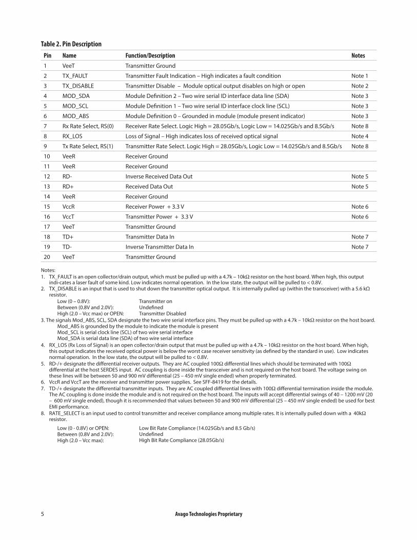
Table 2. Pin Description
Pin Name Function/Description Notes1 VeeT Transmitter Ground
2 TX_FAULT Transmitter Fault Indication – High indicates a fault condition Note 1
3 TX_DISABLE Transmitter Disable – Module optical output disables on high or open Note 2
4 MOD_SDA Module Definition 2 – Two wire serial ID interface data line (SDA) Note 3
5 MOD_SCL Module Definition 1 – Two wire serial ID interface clock line (SCL) Note 3
6 MOD_ABS Module Definition 0 – Grounded in module (module present indicator) Note 3
7 Rx Rate Select, RS(0) Receiver Rate Select. Logic High = 28.05Gb/s, Logic Low = 14.025Gb/s and 8.5Gb/s Note 8
8 RX_LOS Loss of Signal – High indicates loss of received optical signal Note 4
9 Tx Rate Select, RS(1) Transmitter Rate Select. Logic High = 28.05Gb/s, Logic Low = 14.025Gb/s and 8.5Gb/s Note 8
10 VeeR Receiver Ground
11 VeeR Receiver Ground
12 RD- Inverse Received Data Out Note 5
13 RD+ Received Data Out Note 5
14 VeeR Receiver Ground
15 VccR Receiver Power + 3.3 V Note 6
16 VccT Transmitter Power + 3.3 V Note 6
17 VeeT Transmitter Ground
18 TD+ Transmitter Data In Note 7
19 TD- Inverse Transmitter Data In Note 7
20 VeeT Transmitter Ground
Notes:1. TX_FAULT is an open collector/drain output, which must be pulled up with a 4.7k – 10kΩ resistor on the host board. When high, this output
indi-cates a laser fault of some kind. Low indicates normal operation. In the low state, the output will be pulled to < 0.8V.2. TX_DISABLE is an input that is used to shut down the transmitter optical output. It is internally pulled up (within the transceiver) with a 5.6 kΩ
resistor.Low (0 – 0.8V): Transmitter onBetween (0.8V and 2.0V): UndefinedHigh (2.0 – Vcc max) or OPEN: Transmitter Disabled
3. The signals Mod_ABS, SCL, SDA designate the two wire serial interface pins. They must be pulled up with a 4.7k – 10kΩ resistor on the host board. Mod_ABS is grounded by the module to indicate the module is present Mod_SCL is serial clock line (SCL) of two wire serial interface Mod_SDA is serial data line (SDA) of two wire serial interface
4. RX_LOS (Rx Loss of Signal) is an open collector/drain output that must be pulled up with a 4.7k – 10kΩ resistor on the host board. When high, this output indicates the received optical power is below the worst case receiver sensitivity (as defined by the standard in use). Low indicates normal operation. In the low state, the output will be pulled to < 0.8V.
5. RD-/+ designate the differential receiver outputs. They are AC coupled 100Ω differential lines which should be terminated with 100Ωdifferential at the host SERDES input. AC coupling is done inside the transceiver and is not required on the host board. The voltage swing on these lines will be between 50 and 900 mV differential (25 – 450 mV single ended) when properly terminated.
6. VccR and VccT are the receiver and transmitter power supplies. See SFF-8419 for the details.7. TD-/+ designate the differential transmitter inputs. They are AC coupled differential lines with 100Ω differential termination inside the module.
The AC coupling is done inside the module and is not required on the host board. The inputs will accept differential swings of 40 – 1200 mV (20 – 600 mV single ended), though it is recommended that values between 50 and 900 mV differential (25 – 450 mV single ended) be used for best EMI performance.
8. RATE_SELECT is an input used to control transmitter and receiver compliance among multiple rates. It is internally pulled down with a 40kΩ resistor.
Low (0 - 0.8V) or OPEN: Between (0.8V and 2.0V): High (2.0 – Vcc max):
Low Bit Rate Compliance (14.025Gb/s and 8.5 Gb/s) UndefinedHigh Bit Rate Compliance (28.05Gb/s)
Avago Technologies Proprietary 6
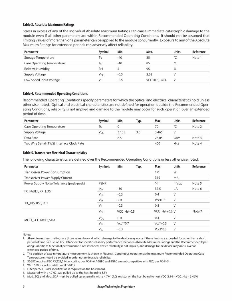
Table 3. Absolute Maximum Ratings
Stress in excess of any of the individual Absolute Maximum Ratings can cause immediate catastrophic damage to the module even if all other parameters are within Recommended Operating Conditions. It should not be assumed that limiting values of more than one parameter can be applied to the module concurrently. Exposure to any of the Absolute Maximum Ratings for extended periods can adversely affect reliability.
Parameter Symbol Min. Max. Units ReferenceStorage Temperature TS -40 85 °C Note 1
Case Operating Temperature TC -40 85 °C
Relative Humidity RH 5 95 %
Supply Voltage VCC -0.5 3.63 V
Low Speed Input Voltage Vi -0.5 VCC+0.5, 3.63 V
Table 4. Recommended Operating Conditions
Recommended Operating Conditions specify parameters for which the optical and electrical characteristics hold unless otherwise noted. Optical and electrical characteristics are not defined for operation outside the Recommended Oper-ating Conditions, reliability is not implied and damage to the module may occur for such operation over an extended period of time.
Parameter Symbol Min. Typ. Max. Units ReferenceCase Operating Temperature Tc 0 70 °C Note 2
Supply Voltage VCC 3.135 3.3 3.465 V
Data Rate 8.5 28.05 Gb/s Note 3
Two Wire Serial (TWS) Interface Clock Rate 400 kHz Note 4
Table 5. Transceiver Electrical Characteristics
The following characteristics are defined over the Recommended Operating Conditions unless otherwise noted.
Parameter Symbols Min. Typ. Max. Units ReferenceTransceiver Power Consumption 1.0 W
Transceiver Power Supply Current 319 mA
Power Supply Noise Tolerance (peak-peak) PSNR 66 mVpp Note 5
Notes:1. Absolute maximum ratings are those values beyond which damage to the device may occur if these limits are exceeded for other than a short
period of time. See Reliability Data Sheet for specific reliability performance. Between Absolute Maximum Ratings and the Recommended Oper-ating Conditions functional performance is not intended, device reliability is not implied, and damage to the device may occur over an extended period of time.
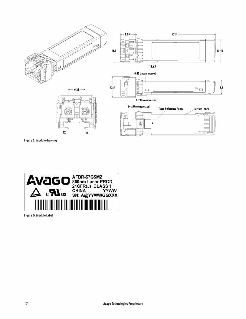
2. The position of case temperature measurement is shown in Figure 5. Continuous operation at the maximum Recommended Operating Case Temperature should be avoided in order not to degrade reliability.
3. 32GFC requires FEC RS(528,514) encoding per FC-PI-6. 16GFC and 8GFC are not compatible with FEC, per FC-PI-5.4. With 500us clock stretch per SFF-84195. Filter per SFF-8419 specification is required on the host board.6. Measured with a 4.7kΩ load pulled up to the host board to 3.3V7. Mod_SCL and Mod_SDA must be pulled up externally with a 4.7k-10kΩ resistor on the host board to host VCC (3.14 < VCC_Hst < 3.46V).
IOH -50 37.5 mA Note 6TX_FAULT, RX_LOS
VOL 0.4 V
TX_DIS, RS0, RS1VIH 2.0 Vcc+0.3 V
Note 7
VIL -0.3 0.8 V
-0.3
VOH VCC_Hst-0.5 VCC_Hst+0.3 V
MOD_SCL, MOD_SDAVOL 0.4 V
VIH V
VIL -0.3 V
0.0
VccT*0.3
VccT+0.5VccT*0.7
Avago Technologies Proprietary 7
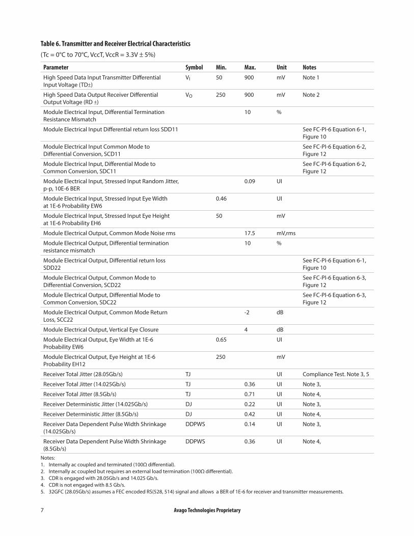
Table 6. Transmitter and Receiver Electrical Characteristics(Tc = 0°C to 70°C, VccT, VccR = 3.3V ± 5%)
Parameter Symbol Min. Max. Unit NotesHigh Speed Data Input Transmitter Differential Input Voltage (TD±)
VI 50 900 mV Note 1
High Speed Data Output Receiver Differential Output Voltage (RD ±)
VO 250 900 mV Note 2
Module Electrical Input, Differential Termination Resistance Mismatch
10 %
Module Electrical Input Differential return loss SDD11 See FC-PI-6 Equation 6-1, Figure 10
Module Electrical Input Common Mode to Differential Conversion, SCD11
See FC-PI-6 Equation 6-2, Figure 12
Module Electrical Input, Differential Mode to Common Conversion, SDC11
See FC-PI-6 Equation 6-2, Figure 12
Module Electrical Input, Stressed Input Random Jitter, p-p, 10E-6 BER
0.09 UI
Module Electrical Input, Stressed Input Eye Width at 1E-6 Probability EW6
0.46 UI
Module Electrical Input, Stressed Input Eye Height at 1E-6 Probability EH6
50 mV
Module Electrical Output, Common Mode Noise rms 17.5 mV,rms
Module Electrical Output, Differential termination resistance mismatch
10 %
Module Electrical Output, Differential return loss SDD22
See FC-PI-6 Equation 6-1, Figure 10
Module Electrical Output, Common Mode to Differential Conversion, SCD22
See FC-PI-6 Equation 6-3, Figure 12
Module Electrical Output, Differential Mode to Common Conversion, SDC22
See FC-PI-6 Equation 6-3, Figure 12
Module Electrical Output, Common Mode Return Loss, SCC22
-2 dB
Module Electrical Output, Vertical Eye Closure 4 dB
Module Electrical Output, Eye Width at 1E-6 Probability EW6
0.65 UI
Module Electrical Output, Eye Height at 1E-6 Probability EH12
250 mV
Receiver Total Jitter (28.05Gb/s) TJ UI Compliance Test. Note 3, 5
Receiver Total Jitter (14.025Gb/s) TJ 0.36 UI Note 3,
Receiver Total Jitter (8.5Gb/s) TJ 0.71 UI Note 4,
Receiver Deterministic Jitter (14.025Gb/s) DJ 0.22 UI Note 3,
Receiver Deterministic Jitter (8.5Gb/s) DJ 0.42 UI Note 4,
Receiver Data Dependent Pulse Width Shrinkage (14.025Gb/s)
DDPWS 0.14 UI Note 3,
Receiver Data Dependent Pulse Width Shrinkage (8.5Gb/s)
DDPWS 0.36 UI Note 4,
Notes:1. Internally ac coupled and terminated (100Ω differential).2. Internally ac coupled but requires an external load termination (100Ω differential).3. CDR is engaged with 28.05Gb/s and 14.025 Gb/s.4. CDR is not engaged with 8.5 Gb/s.5. 32GFC (28.05Gb/s) assumes a FEC encoded RS(528, 514) signal and allows a BER of 1E-6 for receiver and transmitter measurements.
Avago Technologies Proprietary 8
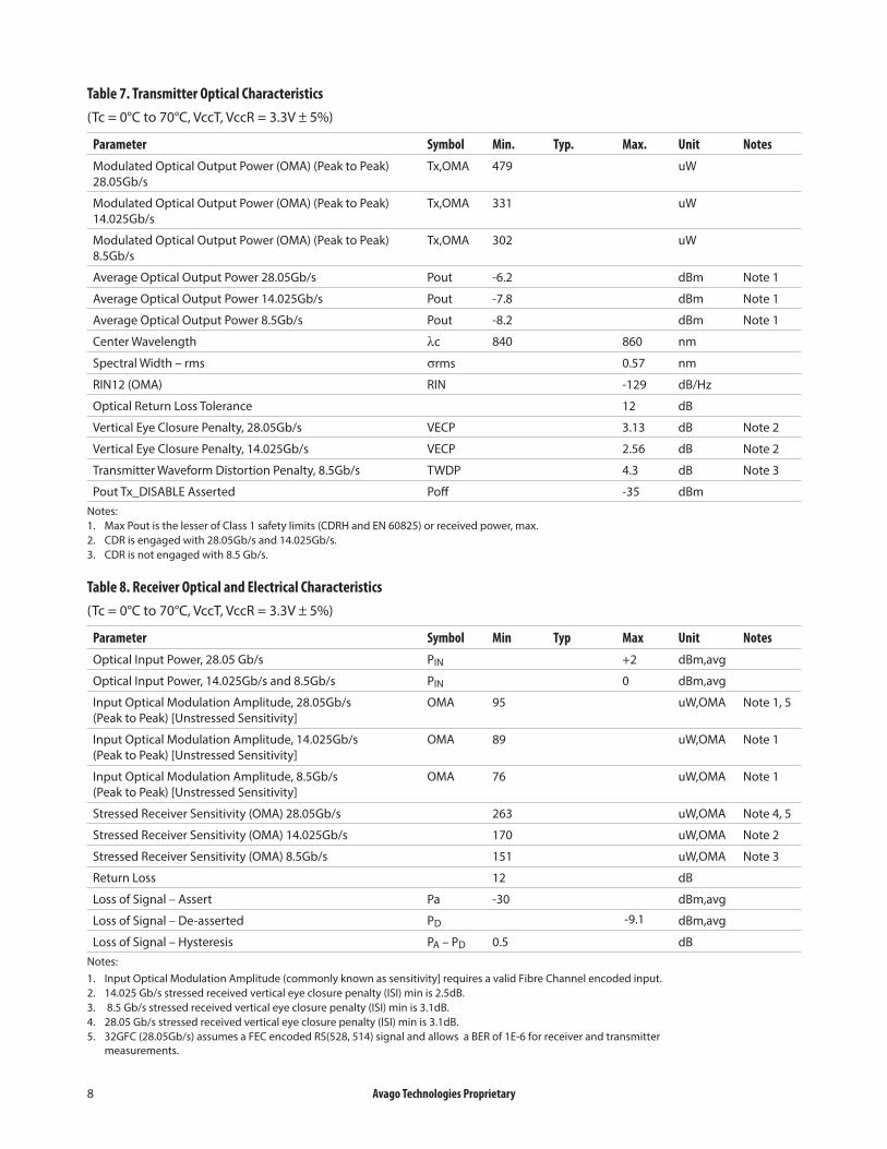
Table 7. Transmitter Optical Characteristics(Tc = 0°C to 70°C, VccT, VccR = 3.3V ± 5%)
Parameter Symbol Min. Typ. Max. Unit NotesModulated Optical Output Power (OMA) (Peak to Peak) 28.05Gb/s
Tx,OMA 479 uW
Modulated Optical Output Power (OMA) (Peak to Peak) 14.025Gb/s
Tx,OMA 331 uW
Modulated Optical Output Power (OMA) (Peak to Peak) 8.5Gb/s
Tx,OMA 302 uW
Average Optical Output Power 28.05Gb/s Pout -6.2 dBm Note 1
Average Optical Output Power 14.025Gb/s Pout -7.8 dBm Note 1
Average Optical Output Power 8.5Gb/s Pout -8.2 dBm Note 1
Center Wavelength λc 840 860 nm
Spectral Width – rms σrms 0.57 nm
RIN12 (OMA) RIN -129 dB/Hz
Optical Return Loss Tolerance 12 dB
Vertical Eye Closure Penalty, 28.05Gb/s VECP 3.13 dB Note 2
Vertical Eye Closure Penalty, 14.025Gb/s VECP 2.56 dB Note 2
Transmitter Waveform Distortion Penalty, 8.5Gb/s TWDP 4.3 dB Note 3
Pout Tx_DISABLE Asserted Poff -35 dBmNotes:1. Max Pout is the lesser of Class 1 safety limits (CDRH and EN 60825) or received power, max.2. CDR is engaged with 28.05Gb/s and 14.025Gb/s.3. CDR is not engaged with 8.5 Gb/s.
Table 8. Receiver Optical and Electrical Characteristics(Tc = 0°C to 70°C, VccT, VccR = 3.3V ± 5%)
Parameter Symbol Min Typ Max Unit NotesOptical Input Power, 28.05 Gb/s PIN +2 dBm,avg
Optical Input Power, 14.025Gb/s and 8.5Gb/s PIN 0 dBm,avg
Input Optical Modulation Amplitude, 28.05Gb/s (Peak to Peak) [Unstressed Sensitivity]
OMA 95 uW,OMA Note 1, 5
Input Optical Modulation Amplitude, 14.025Gb/s (Peak to Peak) [Unstressed Sensitivity]
OMA 89 uW,OMA Note 1
Input Optical Modulation Amplitude, 8.5Gb/s (Peak to Peak) [Unstressed Sensitivity]
OMA 76 uW,OMA Note 1
Stressed Receiver Sensitivity (OMA) 28.05Gb/s 263 uW,OMA Note 4, 5
Stressed Receiver Sensitivity (OMA) 14.025Gb/s 170 uW,OMA Note 2
Stressed Receiver Sensitivity (OMA) 8.5Gb/s 151 uW,OMA Note 3
Return Loss 12 dB
Loss of Signal – Assert Pa -30 dBm,avg
Loss of Signal – De-asserted PD dBm,avg
Loss of Signal – Hysteresis PA – PD 0.5 dBNotes:1. Input Optical Modulation Amplitude (commonly known as sensitivity] requires a valid Fibre Channel encoded input.2. 14.025 Gb/s stressed received vertical eye closure penalty (ISI) min is 2.5dB.3. 8.5 Gb/s stressed received vertical eye closure penalty (ISI) min is 3.1dB.4. 28.05 Gb/s stressed received vertical eye closure penalty (ISI) min is 3.1dB.5. 32GFC (28.05Gb/s) assumes a FEC encoded RS(528, 514) signal and allows a BER of 1E-6 for receiver and transmitter
measurements.
-9.1
Avago Technologies Proprietary 9
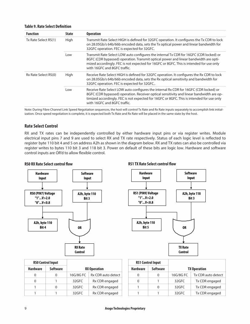
RS0 RX Rate Select control flow
RS0 Control Input
RX OperationHardware Software0 0 16G/8G FC Rx CDR auto detect
0 1 32GFC Rx CDR engaged
1 0 32GFC Rx CDR engaged
1 1 32GFC Rx CDR engaged
RS1 Control Input
TX OperationHardware Software0 0 16G/8G FC Tx CDR auto detect
0 1 32GFC Tx CDR engaged
1 0 32GFC Tx CDR engaged
1 1 32GFC Tx CDR engaged
RS0 (PIN7) Voltage"1"...V>2.0"0"...V<0.8
A2h, byte 110Bit 3
ORA2h, byte 110
Bit 4
RX RateControl
Software Input
Hardware Input
RS1 (PIN9) Voltage"1"...V>2.0"0"...V<0.8
A2h, byte 118Bit 3
ORA2h, byte 110
Bit 5
TX RateControl
Software Input
Hardware Input
Table 9. Rate Select Definition
Function State OperationTx Rate Select RS(1) High Transmit Rate Select HIGH is defined for 32GFC operation. It configures the Tx CDR to lock
on 28.05Gb/s 64b/66b encoded data, sets the Tx optical power and linear bandwidth for 32GFC operation. FEC is expected for 32GFC.
Low Transmit Rate Select LOW auto configures the internal Tx CDR for 16GFC (CDR locked) or 8GFC (CDR bypassed) operation. Transmit optical power and linear bandwidth are opti-mized accordingly. FEC is not expected for 16GFC or 8GFC. This is intended for use only with 16GFC and 8GFC traffic.
Rx Rate Select RS(0) High Receive Rate Select HIGH is defined for 32GFC operation. It configures the Rx CDR to lock on 28.05Gb/s 64b/66b encoded data, sets the Rx optical sensitivity and bandwidth for 32GFC operation. FEC is expected for 32GFC..
Low Receive Rate Select LOW auto configures the internal Rx CDR for 16GFC (CDR locked) or 8GFC (CDR bypassed) operation. Receiver optical sensitivity and linear bandwidth are op-timized accordingly. FEC is not expected for 16GFC or 8GFC. This is intended for use only with 16GFC and 8GFC traffic.
Note: During Fibre Channel Link Speed Negotiation sequences, the host will control Tx Rate and Rx Rate inputs separately to accomplish link initial-ization. Once speed negotiation is complete, it is expected both Tx Rate and Rx Rate will be placed in the same state by the host.
Rate Select ControlRX and TX rates can be independently controlled by either hardware input pins or via register writes. Module electrical input pins 7 and 9 are used to select RX and TX rate respectively. Status of each logic level is reflected to register byte 110 bit 4 and 5 on address A2h as shown in the diagram below. RX and TX rates can also be controlled via register writes to bytes 110 bit 3 and 118 bit 3. Power on default of these bits are logic low. Hardware and software control inputs are OR’d to allow flexible control.
RS1 TX Rate Select control flow
Avago Technologies Proprietary 10
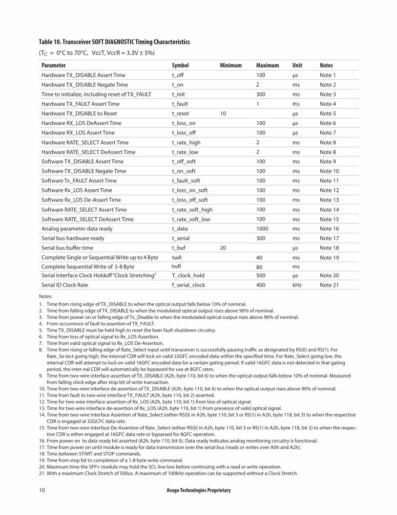
Table 10. Transceiver SOFT DIAGNOSTIC Timing Characteristics (TC
Serial Interface Clock Holdoff “Clock Stretching” T_clock_hold 500 µs Note 20
Serial ID Clock Rate f_serial_clock 400 kHz Note 21
Notes1. Time from rising edge of TX_DISABLE to when the optical output falls below 10% of nominal.2. Time from falling edge of TX_DISABLE to when the modulated optical output rises above 90% of nominal.3. Time from power on or falling edge of Tx_Disable to when the modulated optical output rises above 90% of nominal.4. From occurrence of fault to assertion of TX_FAULT.5. Time TX_DISABLE must be held high to reset the laser fault shutdown circuitry.6. Time from loss of optical signal to Rx_LOS Assertion.7. Time from valid optical signal to Rx_LOS De-Assertion.8. Time from rising or falling edge of Rate_Select input until transceiver is successfully passing traffic as designated by RS(0) and RS(1). For
Rate_Se-lect going high, the internal CDR will lock on valid 32GFC encoded data within the specified time. For Rate_Select going low, the internal CDR will attempt to lock on valid 16GFC encoded data for a certain gating period. If valid 16GFC data is not detected in that gating period, the inter-nal CDR will automatically be bypassed for use at 8GFC rates.
9. Time from two-wire interface assertion of TX_DISABLE (A2h, byte 110, bit 6) to when the optical output falls below 10% of nominal. Measured from falling clock edge after stop bit of write transaction.
10. Time from two-wire interface de-assertion of TX_DISABLE (A2h, byte 110, bit 6) to when the optical output rises above 90% of nominal. 11. Time from fault to two-wire interface TX_FAULT (A2h, byte 110, bit 2) asserted.12. Time for two-wire interface assertion of Rx_LOS (A2h, byte 110, bit 1) from loss of optical signal.13. Time for two-wire interface de-assertion of Rx_LOS (A2h, byte 110, bit 1) from presence of valid optical signal.14. Time from two-wire interface Assertion of Rate_Select (either RS(0) in A2h, byte 110, bit 3 or RS(1) in A2h, byte 118, bit 3) to when the respective
CDR is engaged at 32GCFC data rate.15. Time from two-wire interface De-Assertion of Rate_Select (either RS(0) in A2h, byte 110, bit 3 or RS(1) in A2h, byte 118, bit 3) to when the respec-
tive CDR is either engaged at 16GFC data rate or bypassed for 8GFC operation.16. From power on to data ready bit asserted (A2h, byte 110, bit 0). Data ready indicates analog monitoring circuitry is functional.17. Time from power on until module is ready for data transmission over the serial bus (reads or writes over A0h and A2h).18. Time between START and STOP commands.19. Time from stop bit to completion of a 1-8 byte write command.20. Maximum time the SFP+ module may hold the SCL line low before continuing with a read or write operation.21. With a maximum Clock Stretch of 500us. A maximum of 100kHz operation can be supported without a Clock Stretch.
Complete Sequential Write of 5-8 Byte twR 80 ms
= 0°C to 70°C, VccT, VccR = 3.3V ± 5%)
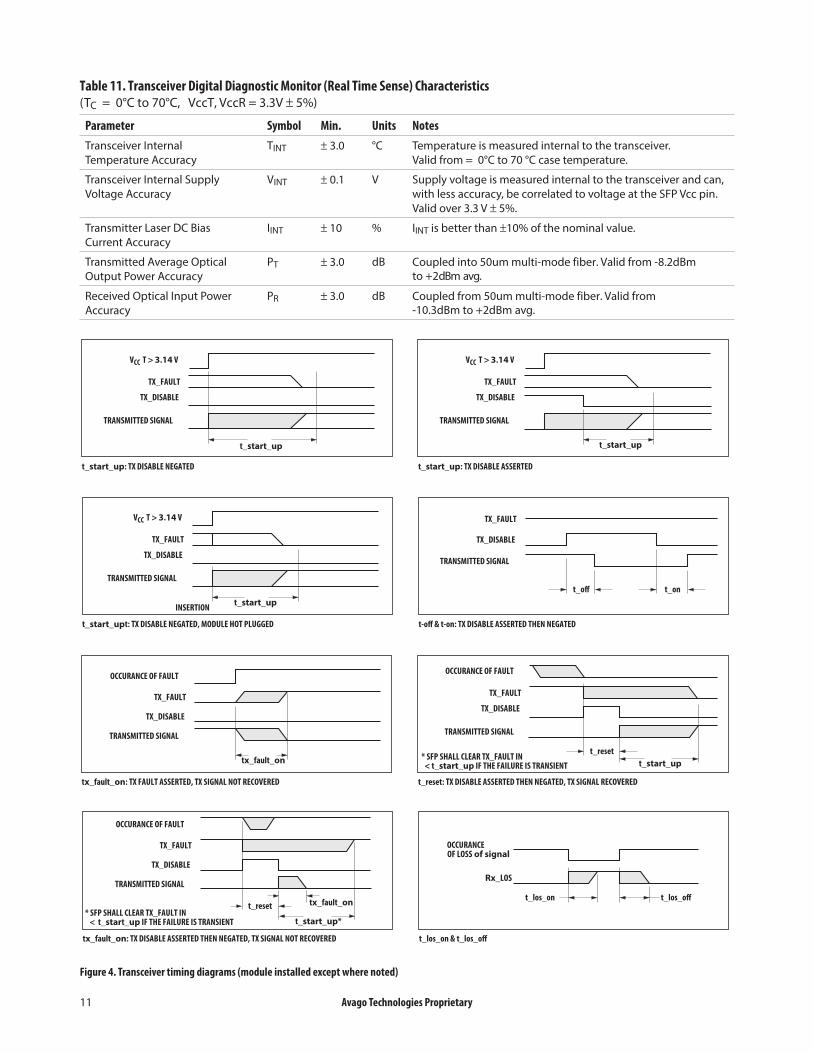
Parameter Symbol Minimum Maximum Unit NotesHardware TX_DISABLE Assert Time t_off 100 µs Note 1
Hardware TX_DISABLE Negate Time t_on 2 ms Note 2
Time to initialize, including reset of TX_FAULT t_init 300 ms Note 3
Hardware TX_FAULT Assert Time t_fault 1 ms Note 4
Hardware TX_DISABLE to Reset t_reset 10 µs Note 5
Hardware RX_LOS DeAssert Time t_loss_on 100 µs Note 6
Hardware RX_LOS Assert Time t_loss_off 100 µs Note 7
Hardware RATE_SELECT Assert Time t_rate_high 2 ms Note 8
Hardware RATE_SELECT DeAssert Time t_rate_low 2 ms Note 8
Software TX_DISABLE Assert Time t_off_soft 100 ms Note 9
Software TX_DISABLE Negate Time t_on_soft 100 ms Note 10
Software Tx_FAULT Assert Time t_fault_soft 100 ms Note 11
Software Rx_LOS Assert Time t_loss_on_soft 100 ms Note 12
Software Rx_LOS De-Assert Time t_loss_off_soft 100 ms Note 13
Software RATE_SELECT Assert Time t_rate_soft_high 100 ms Note 14
Software RATE_SELECT DeAssert Time t_rate_soft_low 100 ms Note 15
Analog parameter data ready t_data 1000 ms Note 16
Serial bus hardware ready t_serial 300 ms Note 17
Serial bus buffer time t_buf 20 µs Note 18
Complete Single or Sequential Write up to 4 Byte twR 40 ms Note 19
Avago Technologies Proprietary 11
Figure 4. Transceiver timing diagrams (module installed except where noted)
Table 11. Transceiver Digital Diagnostic Monitor (Real Time Sense) Characteristics (TC = 0°C to 70°C, VccT, VccR = 3.3V ± 5%)
Parameter Symbol Min. Units NotesTransceiver Internal Temperature Accuracy
TINT ± 3.0 °C Temperature is measured internal to the transceiver. Valid from = 0°C to 70 °C case temperature.
Transceiver Internal Supply Voltage Accuracy
VINT ± 0.1 V Supply voltage is measured internal to the transceiver and can, with less accuracy, be correlated to voltage at the SFP Vcc pin. Valid over 3.3 V ± 5%.
Transmitter Laser DC Bias Current Accuracy
IINT ± 10 % IINT is better than ±10% of the nominal value.
Transmitted Average Optical Output Power Accuracy
PT ± 3.0 dB Coupled into 50um multi-mode fiber. Valid from -8.2dBm to +2dBm avg.
Received Optical Input Power Accuracy
PR ± 3.0 dB Coupled from 50um multi-mode fiber. Valid from -10.3dBm to +2dBm avg.
TX_FAULT
OCCURANCE OF FAULT
tx_fault_on
TX_DISABLE
TRANSMITTED SIGNAL
TX_FAULT
OCCURANCE OF FAULT
TX_DISABLE
TRANSMITTED SIGNAL
tx_fault_on: TX FAULT ASSERTED, TX SIGNAL NOT RECOVERED t_reset: TX DISABLE ASSERTED THEN NEGATED, TX SIGNAL RECOVERED
t_resett_start_up
* SFP SHALL CLEAR TX_FAULT IN< t_start_up IF THE FAILURE IS TRANSIENT
TX_FAULT
OCCURANCE OF FAULT
tx_fault_on
TX_DISABLE
TRANSMITTED SIGNALRx_LOS
tx_fault_on: TX DISABLE ASSERTED THEN NEGATED, TX SIGNAL NOT RECOVERED t_los_on & t_los_o
t_los_on
t_start_up*
t_reset* SFP SHALL CLEAR TX_FAULT IN
< t_start_up IF THE FAILURE IS TRANSIENT
t_los_o
OCCURANCEOF LOSS of signal
TX_FAULT
VCC T > 3.14 V
t_start_up
TX_DISABLE
TRANSMITTED SIGNAL
t_start_up
TX_FAULT
VCC T > 3.14 V
TX_DISABLE
TRANSMITTED SIGNAL
t_start_up: TX DISABLE NEGATED t_start_up: TX DISABLE ASSERTED
TX_FAULT
VCC T > 3.14 V
t_start_up
TX_DISABLE
TRANSMITTED SIGNALt_o
TX_FAULT
TX_DISABLE
TRANSMITTED SIGNAL
t_start_upt: TX DISABLE NEGATED, MODULE HOT PLUGGED t-o & t-on: TX DISABLE ASSERTED THEN NEGATED
INSERTION
t_on
Avago Technologies Proprietary 12
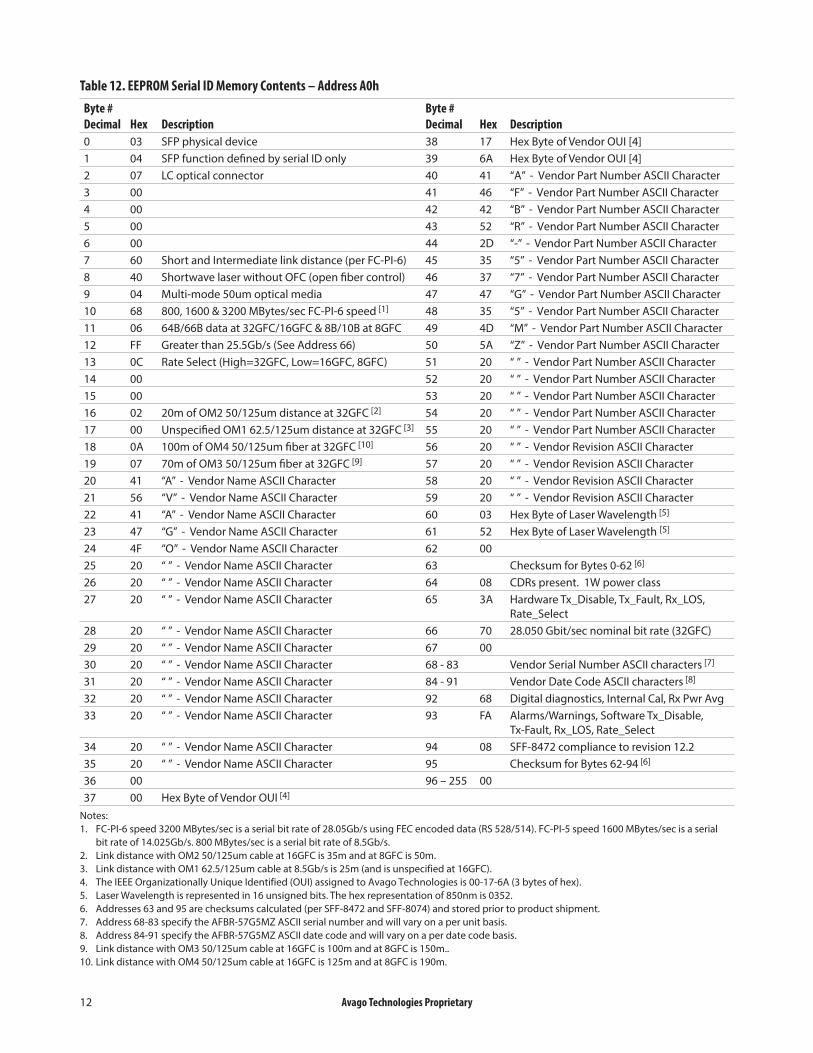
Table 12. EEPROM Serial ID Memory Contents – Address A0h
Byte # Decimal Hex Description
Byte # Decimal Hex Description
0 03 SFP physical device 38 17 Hex Byte of Vendor OUI [4]1 04 SFP function defined by serial ID only 39 6A Hex Byte of Vendor OUI [4]2 07 LC optical connector 40 41 “A” - Vendor Part Number ASCII Character3 00 41 46 “F” - Vendor Part Number ASCII Character4 00 42 42 “B” - Vendor Part Number ASCII Character5 00 43 52 “R” - Vendor Part Number ASCII Character6 00 44 2D “-” - Vendor Part Number ASCII Character7 60 Short and Intermediate link distance (per FC-PI-6) 45 35 “5” - Vendor Part Number ASCII Character8 40 Shortwave laser without OFC (open fiber control) 46 37 “7” - Vendor Part Number ASCII Character9 04 Multi-mode 50um optical media 47 47 “G” - Vendor Part Number ASCII Character10 68 800, 1600 & 3200 MBytes/sec FC-PI-6 speed [1] 48 35 “5” - Vendor Part Number ASCII Character11 06 64B/66B data at 32GFC/16GFC & 8B/10B at 8GFC 49 4D “M” - Vendor Part Number ASCII Character12 FF Greater than 25.5Gb/s (See Address 66) 50 5A “Z” - Vendor Part Number ASCII Character13 0C Rate Select (High=32GFC, Low=16GFC, 8GFC) 51 20 “ ” - Vendor Part Number ASCII Character14 00 52 20 “ ” - Vendor Part Number ASCII Character15 00 53 20 “ ” - Vendor Part Number ASCII Character16 02 20m of OM2 50/125um distance at 32GFC [2] 54 20 “ ” - Vendor Part Number ASCII Character17 00 Unspecified OM1 62.5/125um distance at 32GFC [3] 55 20 “ ” - Vendor Part Number ASCII Character18 0A 100m of OM4 50/125um fiber at 32GFC [10] 56 20 “ ” - Vendor Revision ASCII Character19 07 70m of OM3 50/125um fiber at 32GFC [9] 57 20 “ ” - Vendor Revision ASCII Character20 41 “A” - Vendor Name ASCII Character 58 20 “ ” - Vendor Revision ASCII Character21 56 “V” - Vendor Name ASCII Character 59 20 “ ” - Vendor Revision ASCII Character22 41 “A” - Vendor Name ASCII Character 60 03 Hex Byte of Laser Wavelength [5]
23 47 “G” - Vendor Name ASCII Character 61 52 Hex Byte of Laser Wavelength [5]
24 4F “O” - Vendor Name ASCII Character 62 0025 20 “ ” - Vendor Name ASCII Character 63 Checksum for Bytes 0-62 [6]
26 20 “ ” - Vendor Name ASCII Character 64 08 CDRs present. 1W power class27 20 “ ” - Vendor Name ASCII Character 65 3A Hardware Tx_Disable, Tx_Fault, Rx_LOS,
Rate_Select28 20 “ ” - Vendor Name ASCII Character 66 70 28.050 Gbit/sec nominal bit rate (32GFC)29 20 “ ” - Vendor Name ASCII Character 67 0030 20 “ ” - Vendor Name ASCII Character 68 - 83 Vendor Serial Number ASCII characters [7]
31 20 “ ” - Vendor Name ASCII Character 84 - 91 Vendor Date Code ASCII characters [8]
32 20 “ ” - Vendor Name ASCII Character 92 68 Digital diagnostics, Internal Cal, Rx Pwr Avg33 20 “ ” - Vendor Name ASCII Character 93 FA Alarms/Warnings, Software Tx_Disable,
Tx-Fault, Rx_LOS, Rate_Select34 20 “ ” - Vendor Name ASCII Character 94 08 SFF-8472 compliance to revision 12.235 20 “ ” - Vendor Name ASCII Character 95 Checksum for Bytes 62-94 [6]
36 00 96 – 255 0037 00 Hex Byte of Vendor OUI [4]
Notes:1. FC-PI-6 speed 3200 MBytes/sec is a serial bit rate of 28.05Gb/s using FEC encoded data (RS 528/514). FC-PI-5 speed 1600 MBytes/sec is a serial
bit rate of 14.025Gb/s. 800 MBytes/sec is a serial bit rate of 8.5Gb/s. 2. Link distance with OM2 50/125um cable at 16GFC is 35m and at 8GFC is 50m. 3. Link distance with OM1 62.5/125um cable at 8.5Gb/s is 25m (and is unspecified at 16GFC).4. The IEEE Organizationally Unique Identified (OUI) assigned to Avago Technologies is 00-17-6A (3 bytes of hex).5. Laser Wavelength is represented in 16 unsigned bits. The hex representation of 850nm is 0352.6. Addresses 63 and 95 are checksums calculated (per SFF-8472 and SFF-8074) and stored prior to product shipment.7. Address 68-83 specify the AFBR-57G5MZ ASCII serial number and will vary on a per unit basis.8. Address 84-91 specify the AFBR-57G5MZ ASCII date code and will vary on a per date code basis.9. Link distance with OM3 50/125um cable at 16GFC is 100m and at 8GFC is 150m..10. Link distance with OM4 50/125um cable at 16GFC is 125m and at 8GFC is 190m.
Avago Technologies Proprietary 13
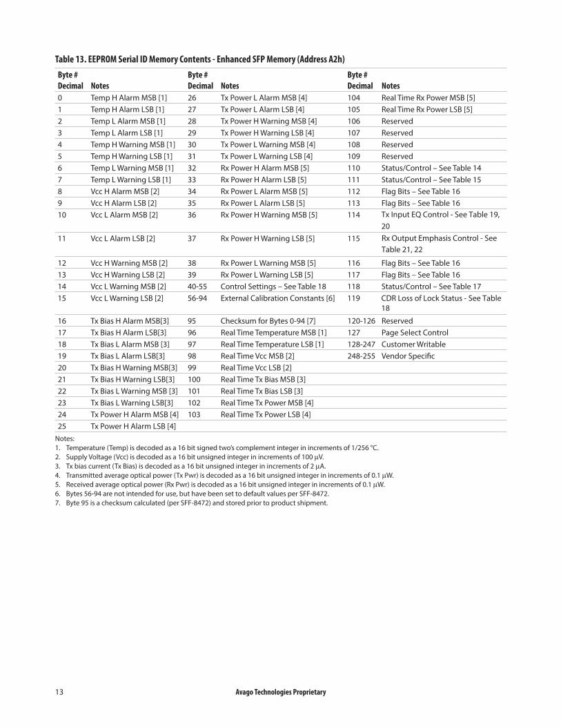
Table 13. EEPROM Serial ID Memory Contents - Enhanced SFP Memory (Address A2h)
Byte # Decimal Notes
Byte # Decimal Notes
Byte # Decimal Notes
0 Temp H Alarm MSB [1] 26 Tx Power L Alarm MSB [4] 104 Real Time Rx Power MSB [5]1 Temp H Alarm LSB [1] 27 Tx Power L Alarm LSB [4] 105 Real Time Rx Power LSB [5]2 Temp L Alarm MSB [1] 28 Tx Power H Warning MSB [4] 106 Reserved3 Temp L Alarm LSB [1] 29 Tx Power H Warning LSB [4] 107 Reserved4 Temp H Warning MSB [1] 30 Tx Power L Warning MSB [4] 108 Reserved5 Temp H Warning LSB [1] 31 Tx Power L Warning LSB [4] 109 Reserved6 Temp L Warning MSB [1] 32 Rx Power H Alarm MSB [5] 110 Status/Control – See Table 147 Temp L Warning LSB [1] 33 Rx Power H Alarm LSB [5] 111 Status/Control – See Table 158 Vcc H Alarm MSB [2] 34 Rx Power L Alarm MSB [5] 112 Flag Bits – See Table 169 Vcc H Alarm LSB [2] 35 Rx Power L Alarm LSB [5] 113 Flag Bits – See Table 1610 Vcc L Alarm MSB [2] 36 Rx Power H Warning MSB [5] 114
11 Vcc L Alarm LSB [2] 37 Rx Power H Warning LSB [5] 115
Tx Input EQ Control - See Table 19, 20
12 Vcc H Warning MSB [2] 38 Rx Power L Warning MSB [5] 116 Flag Bits – See Table 1613 Vcc H Warning LSB [2] 39 Rx Power L Warning LSB [5] 117 Flag Bits – See Table 1614 Vcc L Warning MSB [2] 40-55 Control Settings – See Table 18 118 Status/Control – See Table 1715 Vcc L Warning LSB [2] 56-94 External Calibration Constants [6] 119 CDR Loss of Lock Status - See Table
18
16 Tx Bias H Alarm MSB[3] 95 Checksum for Bytes 0-94 [7] 120-126 Reserved17 Tx Bias H Alarm LSB[3] 96 Real Time Temperature MSB [1] 127 Page Select Control18 Tx Bias L Alarm MSB [3] 97 Real Time Temperature LSB [1] 128-247 Customer Writable19 Tx Bias L Alarm LSB[3] 98 Real Time Vcc MSB [2] 248-255 Vendor Specific20 Tx Bias H Warning MSB[3] 99 Real Time Vcc LSB [2]21 Tx Bias H Warning LSB[3] 100 Real Time Tx Bias MSB [3]22 Tx Bias L Warning MSB [3] 101 Real Time Tx Bias LSB [3]23 Tx Bias L Warning LSB[3] 102 Real Time Tx Power MSB [4]24 Tx Power H Alarm MSB [4] 103 Real Time Tx Power LSB [4]25 Tx Power H Alarm LSB [4]
Notes:1. Temperature (Temp) is decoded as a 16 bit signed two’s complement integer in increments of 1/256 °C.2. Supply Voltage (Vcc) is decoded as a 16 bit unsigned integer in increments of 100 µV.3. Tx bias current (Tx Bias) is decoded as a 16 bit unsigned integer in increments of 2 µA.4. Transmitted average optical power (Tx Pwr) is decoded as a 16 bit unsigned integer in increments of 0.1 µW.5. Received average optical power (Rx Pwr) is decoded as a 16 bit unsigned integer in increments of 0.1 µW.6. Bytes 56-94 are not intended for use, but have been set to default values per SFF-8472.7. Byte 95 is a checksum calculated (per SFF-8472) and stored prior to product shipment.
Rx Output Emphasis Control - See Table 21, 22
Avago Technologies Proprietary 14
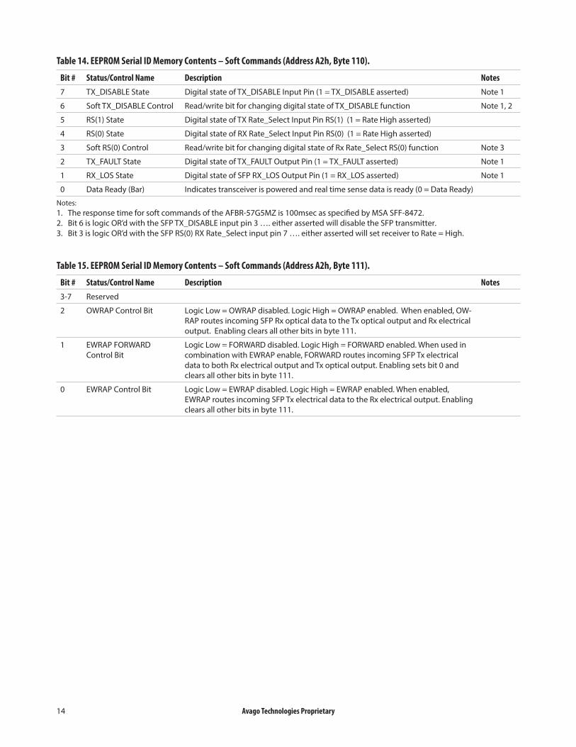
Table 14. EEPROM Serial ID Memory Contents – Soft Commands (Address A2h, Byte 110).
Bit # Status/Control Name Description Notes7 TX_DISABLE State Digital state of TX_DISABLE Input Pin (1 = TX_DISABLE asserted) Note 1
6 Soft TX_DISABLE Control Read/write bit for changing digital state of TX_DISABLE function Note 1, 2
5 RS(1) State Digital state of TX Rate_Select Input Pin RS(1) (1 = Rate High asserted)
4 RS(0) State Digital state of RX Rate_Select Input Pin RS(0) (1 = Rate High asserted)
3 Soft RS(0) Control Read/write bit for changing digital state of Rx Rate_Select RS(0) function Note 3
2 TX_FAULT State Digital state of TX_FAULT Output Pin (1 = TX_FAULT asserted) Note 1
1 RX_LOS State Digital state of SFP RX_LOS Output Pin (1 = RX_LOS asserted) Note 1
0 Data Ready (Bar) Indicates transceiver is powered and real time sense data is ready (0 = Data Ready)
Notes:1. The response time for soft commands of the AFBR-57G5MZ is 100msec as specified by MSA SFF-8472.2. Bit 6 is logic OR’d with the SFP TX_DISABLE input pin 3 …. either asserted will disable the SFP transmitter.3. Bit 3 is logic OR’d with the SFP RS(0) RX Rate_Select input pin 7 …. either asserted will set receiver to Rate = High.
Table 15. EEPROM Serial ID Memory Contents – Soft Commands (Address A2h, Byte 111).
Bit # Status/Control Name Description Notes3-7 Reserved
2 OWRAP Control Bit Logic Low = OWRAP disabled. Logic High = OWRAP enabled. When enabled, OW-RAP routes incoming SFP Rx optical data to the Tx optical output and Rx electrical output. Enabling clears all other bits in byte 111.
1 EWRAP FORWARD Control Bit
Logic Low = FORWARD disabled. Logic High = FORWARD enabled. When used in combination with EWRAP enable, FORWARD routes incoming SFP Tx electrical data to both Rx electrical output and Tx optical output. Enabling sets bit 0 and clears all other bits in byte 111.
0 EWRAP Control Bit Logic Low = EWRAP disabled. Logic High = EWRAP enabled. When enabled, EWRAP routes incoming SFP Tx electrical data to the Rx electrical output. Enabling clears all other bits in byte 111.
Avago Technologies Proprietary 15
Table 16. EEPROM Serial ID Memory Contents – Alarms and Warnings (Address A2h, Bytes 112, 113, 116, 117)
Byte Bit Flag Bit Name Description112 7 Temp High Alarm Set when transceiver internal temperature exceeds high alarm threshold.
6 Temp Low Alarm Set when transceiver internal temperature exceeds low alarm threshold.
5 Vcc High Alarm Set when transceiver internal supply voltage exceeds high alarm threshold.
4 Vcc Low Alarm Set when transceiver internal supply voltage exceeds low alarm threshold.
3 Tx Bias High Alarm Set when transceiver laser bias current exceeds high alarm threshold.
2 Tx Bias Low Alarm Set when transceiver laser bias current exceeds low alarm threshold.
1 Tx Power High Alarm Set when transmitted average optical power exceeds high alarm threshold.
0 Tx Power Low Alarm Set when transmitted average optical power exceeds low alarm threshold.
113 7 Rx Power High Alarm Set when received average optical power exceeds high alarm threshold.
6 Rx Power Low Alarm Set when received average optical power exceeds low alarm threshold.
0-5 reserved
116 7 Temp High Warning Set when transceiver internal temperature exceeds high warning threshold.
6 Temp Low Warning Set when transceiver internal temperature exceeds low warning threshold.
5 Vcc High Warning Set when transceiver internal supply voltage exceeds high warning threshold.
4 Vcc Low Warning Set when transceiver internal supply voltage exceeds low warning threshold.
3 Tx Bias High Warning Set when transceiver laser bias current exceeds high warning threshold.
2 Tx Bias Low Warning Set when transceiver laser bias current exceeds low warning threshold.
1 Tx Power High Warning Set when transmitted average optical power exceeds high warning threshold.
0 Tx Power Low Warning Set when transmitted average optical power exceeds low warning threshold.
117 7 Rx Power High Warning Set when received average optical power exceeds high warning threshold.
6 Rx Power Low Warning Set when received average optical power exceeds low warning threshold.
0-5 reserved
Table 17. EEPROM Serial ID Memory Contents – Soft Commands (Address A2h, Byte 118).
Bit # Status/Control Name Description Notes4-7 Reserved
3 Soft RS(1) Control Read/write bit for changing digital state of Tx Rate_Select RS(1) function Note 1
2 Reserved
1 Power Level State Always set to zero. Value of zero indicates Power Level 1 operation (1 Watt max)
0 Power Level Select Unused. This device supports power level zero (1 Watt max) only.
Notes:1. Bit 3 is log OR’d with the SFP RS(1) TX Rate_Select input pin 9 …. either asserted will set transmitter to Rate = High.
Table 18. EEPROM Serial ID Memory Contents – CDR Loss of Lock (LOL) Status Indicators (Address A2h, Byte 119).
Bit # Status/Control Name Description Notes7-2 Reserved
1 Tx CDR LOL Flag A value of 0 indicates the CDR is locked. A value of 1 indicates CDR loss of lock. If the CDR is operationally bypassed (ie. for 8.5Gb/s operation), value is undefined.
0 Rx CDR LOL Flag A value of 0 indicates the CDR is locked. A value of 1 indicates CDR loss of lock. If the CDR is operationally bypassed (ie. for 8.5Gb/s operation), value is undefined.
Avago Technologies Proprietary 16
Table 19. EEPROM Serial ID Memory Contents – Transmitter Input Electrical Equalization Control (Address A2h, Byte 114).
Bit # Status/Control Name Description7-4 TX EQ, RS(1)=HIGH Selects an input equalization value per Table 9-13 of SFF-8472 for high rate operation.
3-0 TX EQ, RS(1)=LOW Selects an input equalization value per Table 9-13 of SFF-8472 for low rate operation.
Table 20. Transmitter Input Equalization Control Values (Address A2h, Byte 114)From Table 9-13 of SFF-8472
Code
Transmitter Input Equalization
Nominal Units11xx Reserved
1011 Reserved
1010 10 dB
1001 9 dB
1000 8 dB
0111 7 dB
0110 6 dB
0101 5 dB
0100 4 dB
0011 3 dB
0010 2 dB
0001 1 dB
0000 0 No Equalization
Table 21. EEPROM Serial ID Memory Contents – Receiver Output Electrical Emphasis Control (Address A2h, Byte 115).
Bit # Status/Control Name Description7-4 RX EMPH, RS(0)=HIGH Selects an output emphasis value per Table 9-14 of SFF-8472 for high rate operation.
3-0 RX EMPH, RS(0)=LOW Selects an output emphasis value per Table 9-14 of SFF-8472 for low rate operation.
Table 22. Receiver Output Emphasis Control Values (Address A2h, Byte 115)From Table 9-14 of SFF-8472
Code
Receiver Output EmphasisAt nominal Output Amplitude
Nominal Units1xxx Vendor Specific
0111 7 dB
0110 6 dB
0101 5 dB
0100 4 dB
0011 3 dB
0010 2 dB
0001 1 dB
0000 0 No Emphasis
Avago Technologies Proprietary 17
Figure 5. Module drawing
47.5
13.9
8.99
13.65
13.46
8.512.5
0.65 Uncompressed
0.7 Uncompressed
Bottom LabelTcase Reference Point14.8 Uncompressed
TX RX
6.25
Figure 6. Module Label
Avago Technologies Proprietary 18
2x 1.7
20x 0.5 ± 0.030.9
2 ± 0.005 TYP.0.06
10.5311.93
20
1011
PIN 1
20
10 11
PIN 1
0.8TYP .
10.939.6
2x 1.55 ± 0.05
3.25
4
32
1
1
26.8 511x 2.0
103x
41.3
42.3
B
10x 1.05 ± 0.01
16.25REF . 14.25
11.088.58
5.68
2.011x
11.939.6
4.8
8.48
A
3.68
SEE DETAIL 1
9x 0.95 ± 0.05
2.5
7.17.2
2.5
103x
34.5
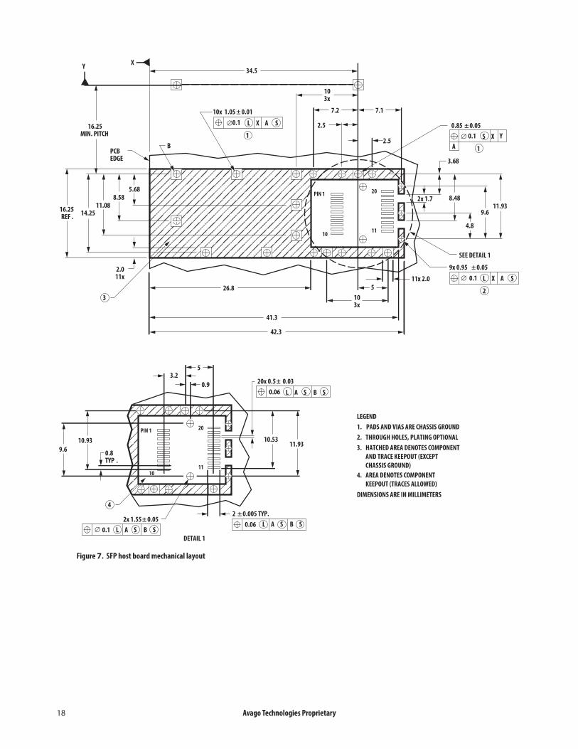
16.25MIN. PITCH
Y X
DETAIL 1
Figure 7. SFP host board mechanical layout
0.85 ± 0.05
PCBEDGE
0.06
0.1
0.1
0.1
0.1 Y
∅
∅
∅
∅
LEGEND1. PADS AND VIAS ARE CHASSIS GROUND2. THROUGH HOLES, PLATING OPTIONAL3. HATCHED AREA DENOTES COMPONENT
AND TRACE KEEPOUT (EXCEPTCHASSIS GROUND)
4. AREA DENOTES COMPONENTKEEPOUT (TRACES ALLOWED)
DIMENSIONS ARE IN MILLIMETERS
L X A S
L X A S
S X
L A S B S
L A S B SL A S B S
Avago Technologies Proprietary
42.08 ± 0.5
3.5 ± 0.31.7 ± 0.9
10
15.25 ± 0.1
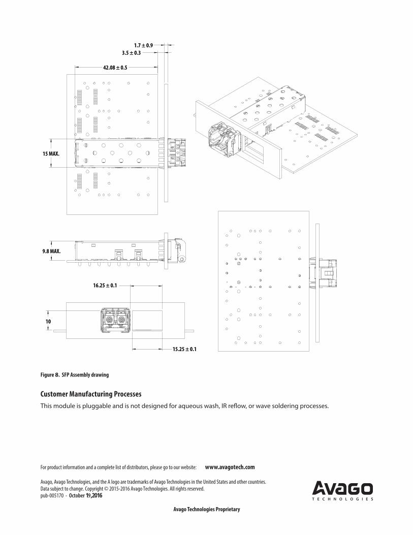
Figure 8. SFP Assembly drawing
Customer Manufacturing ProcessesThis module is pluggable and is not designed for aqueous wash, IR reflow, or wave soldering processes.
9.8 MAX.
15 MAX.
16.25 ± 0.1
For product information and a complete list of distributors, please go to our website: www.avagotech.com
Avago, Avago Technologies, and the A logo are trademarks of Avago Technologies in the United States and other countries. Data subject to change. Copyright © 2015-2016 Avago Technologies. All rights reserved. pub-005170 - October 19,2016