Embed Size (px)
Citation preview

AFE840x System Evaluation Kit and GC StudioReference
User's Guide
Literature Number: SLWU034AMay 2006–Revised November 2008

2 SLWU034A–May 2006–Revised November 2008Submit Documentation Feedback

Contents
1 AFE840x System Evaluation Kit (SEK) Overview ............................................................ 51.1 AFE840x System Evaluation Kit ........................................................................................... 6
2 Installing the Software ................................................................................................ 72.1 TSW2100 SPI Software Installation ....................................................................................... 72.2 GC Studio Software Installation............................................................................................ 7
3 Setting up the System ................................................................................................. 93.1 Hardware Setup.............................................................................................................. 93.2 Loading and Running a GC Studio Project ............................................................................. 12
3.2.1 ADC Experiments: AFE840x_TESTBUS_EX Directory ...................................................... 123.2.2 UMTS Experiment: AFE840x_UMTS_EX Directory .......................................................... 123.2.3 CDMA2000 Experiment: AFE840x_CDMA2k_EX Directory................................................. 123.2.4 DDC AGC Experiment: AFE840x_AGC_EX Directory ....................................................... 123.2.5 ADC Experiment: AFE840x_ADC_EX Directory .............................................................. 133.2.6 Parallel Port Output Experiment: AFE840x_Parallel_Output_EX Directory ............................... 13
3.3 Creating a New GC Studio Project....................................................................................... 15
4 Other Options in GC Studio ....................................................................................... 334.1 Saving the Output to a File................................................................................................ 334.2 Changing the Data Capture Size......................................................................................... 344.3 Capturing the AFE840x Test Bus Output ............................................................................... 36
5 AFE840x Daughtercard Description ............................................................................ 415.1 AFE840x Daughtercard Pin Description................................................................................. 415.2 AFE840x Daughtercard Jumpers ........................................................................................ 435.3 AFE840x Daughtercard Power Supplies ................................................................................ 435.4 AFE840x Daughtercard Clock Configurations.......................................................................... 43
Important Notices ............................................................................................................... 45
SLWU034A–May 2006–Revised November 2008 Contents 3Submit Documentation Feedback
www.ti.com
List of Figures1-1 Kit Contents................................................................................................................... 63-1 System Setup ............................................................................................................... 103-2 Typical Setup ............................................................................................................... 113-3 TSW2100 SPI Software Screen.......................................................................................... 12
List of Tables3-1 Clock Requirements ......................................................................................................... 93-2 SMA Cable Connections .................................................................................................. 103-3 Default Jumper Settings ................................................................................................... 105-1 Memory Input Bus—36 Data Inputs Used to Stimulate the AFE840x Inputs....................................... 425-2 Memory Output Bus—36 Data Outputs From Selected AFE840x Outputs Captured by the GC101 ........... 425-3 Clock ......................................................................................................................... 425-4 Microprocessor Control Bus—Bus to Program the Internal Registers .............................................. 425-5 JTAG ......................................................................................................................... 425-6 Power and Ground ......................................................................................................... 42
4 List of Figures SLWU034A–May 2006–Revised November 2008Submit Documentation Feedback
C001
Chapter 1SLWU034A–May 2006–Revised November 2008
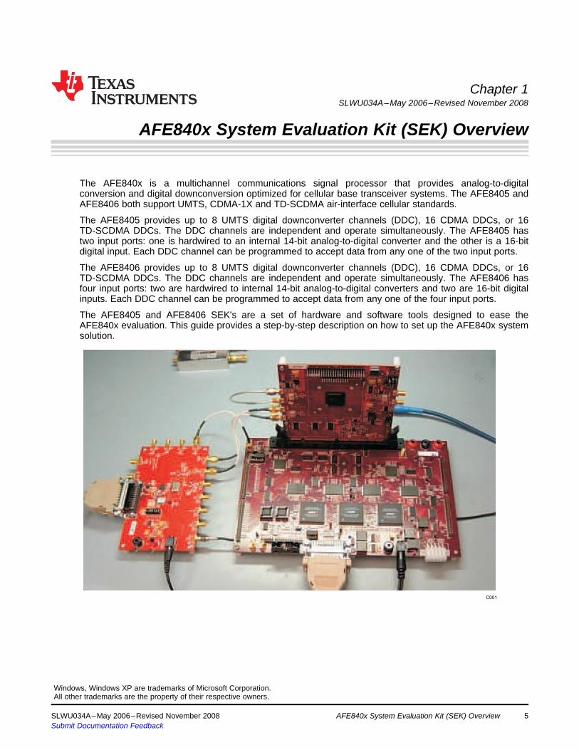
AFE840x System Evaluation Kit (SEK) Overview
The AFE840x is a multichannel communications signal processor that provides analog-to-digitalconversion and digital downconversion optimized for cellular base transceiver systems. The AFE8405 andAFE8406 both support UMTS, CDMA-1X and TD-SCDMA air-interface cellular standards.
The AFE8405 provides up to 8 UMTS digital downconverter channels (DDC), 16 CDMA DDCs, or 16TD-SCDMA DDCs. The DDC channels are independent and operate simultaneously. The AFE8405 hastwo input ports: one is hardwired to an internal 14-bit analog-to-digital converter and the other is a 16-bitdigital input. Each DDC channel can be programmed to accept data from any one of the two input ports.
The AFE8406 provides up to 8 UMTS digital downconverter channels (DDC), 16 CDMA DDCs, or 16TD-SCDMA DDCs. The DDC channels are independent and operate simultaneously. The AFE8406 hasfour input ports: two are hardwired to internal 14-bit analog-to-digital converters and two are 16-bit digitalinputs. Each DDC channel can be programmed to accept data from any one of the four input ports.
The AFE8405 and AFE8406 SEK's are a set of hardware and software tools designed to ease theAFE840x evaluation. This guide provides a step-by-step description on how to set up the AFE840x systemsolution.
Windows, Windows XP are trademarks of Microsoft Corporation.All other trademarks are the property of their respective owners.
SLWU034A–May 2006–Revised November 2008 AFE840x System Evaluation Kit (SEK) Overview 5Submit Documentation Feedback
1.1 AFE840x System Evaluation Kit
M0050-01
SMA cables
5-V power supply for TSW2100
GC101 motherboard
5-V power supply for GC101
AFE840x daughtercard
TSW2100 clock solution EVM
Parallel port cable Software CD
AFE840x System Evaluation Kit www.ti.com
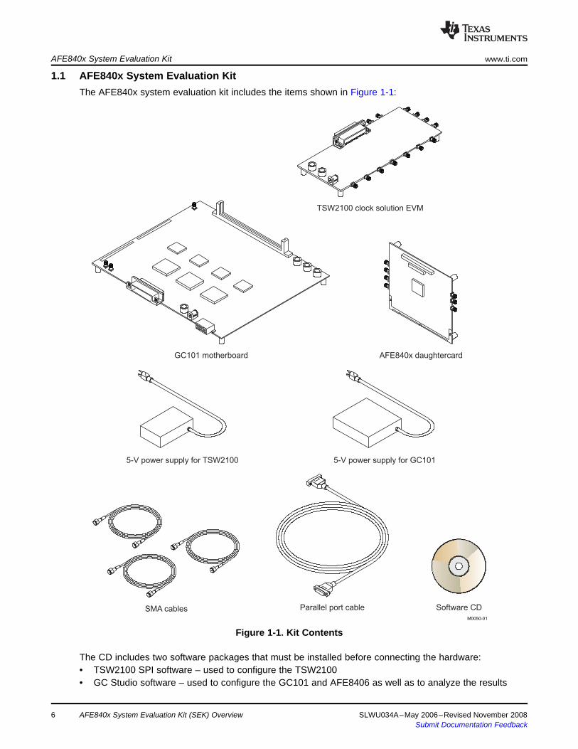
The AFE840x system evaluation kit includes the items shown in Figure 1-1:
Figure 1-1. Kit Contents
The CD includes two software packages that must be installed before connecting the hardware:• TSW2100 SPI software – used to configure the TSW2100• GC Studio software – used to configure the GC101 and AFE8406 as well as to analyze the results
6 AFE840x System Evaluation Kit (SEK) Overview SLWU034A–May 2006–Revised November 2008Submit Documentation Feedback
2.1 TSW2100 SPI Software Installation
C049
2.2 GC Studio Software Installation
Chapter 2SLWU034A–May 2006–Revised November 2008
Installing the Software
All necessary software to operate the serial interface is provided on the included CD. This sectiondescribes in detail how to install the required software packages.
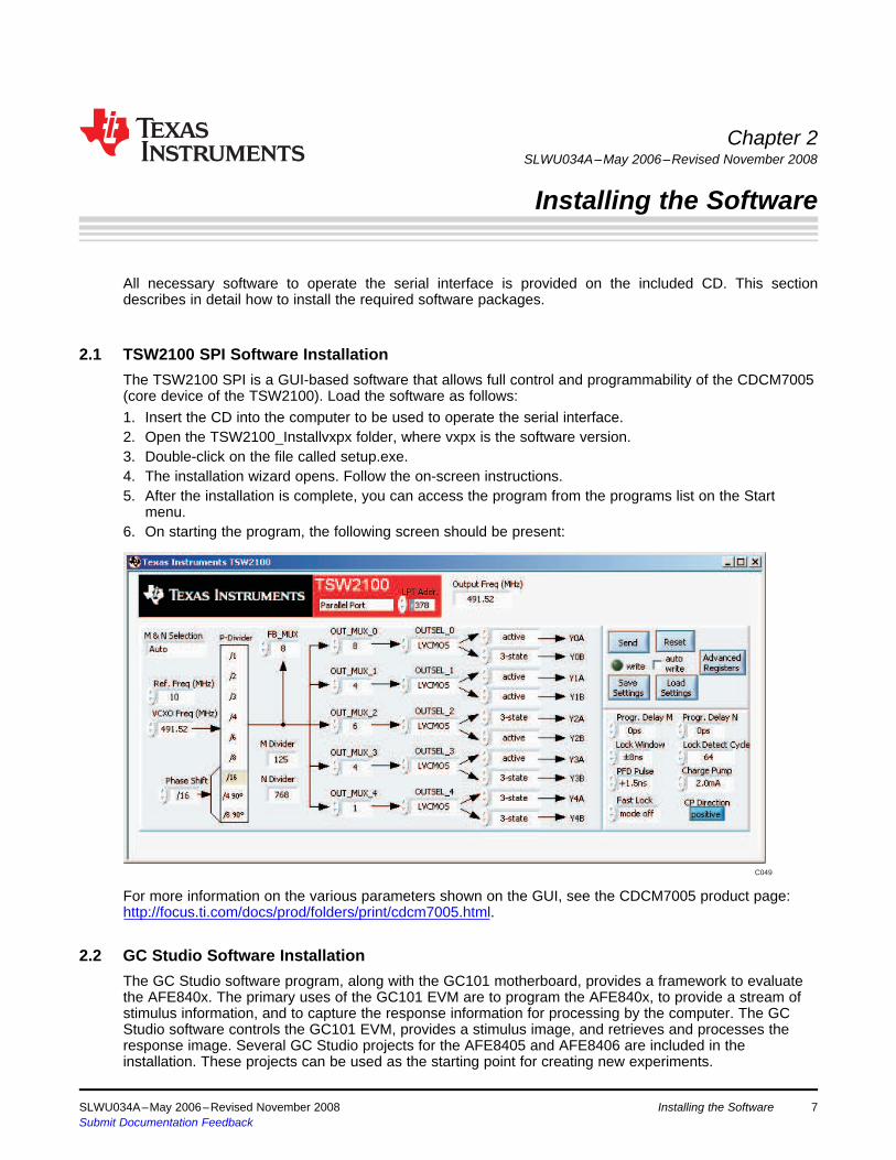
The TSW2100 SPI is a GUI-based software that allows full control and programmability of the CDCM7005(core device of the TSW2100). Load the software as follows:1. Insert the CD into the computer to be used to operate the serial interface.2. Open the TSW2100_Installvxpx folder, where vxpx is the software version.3. Double-click on the file called setup.exe.4. The installation wizard opens. Follow the on-screen instructions.5. After the installation is complete, you can access the program from the programs list on the Start
menu.6. On starting the program, the following screen should be present:
For more information on the various parameters shown on the GUI, see the CDCM7005 product page:http://focus.ti.com/docs/prod/folders/print/cdcm7005.html.
The GC Studio software program, along with the GC101 motherboard, provides a framework to evaluatethe AFE840x. The primary uses of the GC101 EVM are to program the AFE840x, to provide a stream ofstimulus information, and to capture the response information for processing by the computer. The GCStudio software controls the GC101 EVM, provides a stimulus image, and retrieves and processes theresponse image. Several GC Studio projects for the AFE8405 and AFE8406 are included in theinstallation. These projects can be used as the starting point for creating new experiments.
SLWU034A–May 2006–Revised November 2008 Installing the Software 7Submit Documentation Feedback

C003
GC Studio Software Installation www.ti.com
The minimum requirements to install GC Studio are:• Host computer (PC) with BIOS supporting ECP mode for LPT1, running Windows™ 98 SP 2, Windows
ME, Windows 2000 SP 1, Windows XP™ Home or Windows XP Professional• Administrator group privileges
The steps to install GC Studio are as follows:1. Insert the CD into the computer to be used to operate the serial interface.2. Double-click the file called GCStudio_Setup_xx_xx_xxxxxx.exe, where xx_xx_xxxx corresponds to the
GC Studio version number.3. The installation wizard opens. Follow the on-screen instructions. This loads the main GC Studio
software.4. After the installation is complete, you can access the program from the programs list on the Start
menu.5. To start the program, click on the Windows menu sequence Start - All Programs - GC Studio - GC
Studio. On starting the program, the following screen should be present:
8 Installing the Software SLWU034A–May 2006–Revised November 2008Submit Documentation Feedback
3.1 Hardware Setup
Chapter 3SLWU034A–May 2006–Revised November 2008
Setting up the System
The GC101 and AFE840x daughtercard require three clocks when used for operation with an analog inputsignal. The clocks are described in Table 3-1.
Table 3-1. Clock RequirementsBOARD CONNECTOR DESCRIPTION
AFE840x daughtercard CLKP (J6) AFE840x ADC clock. On the AFE840x daughtercard, thissignal is converted to a differential signal and routed toAFE840x balls CLK(M/P)(A/B). It must be a low-jitter clockfor optimal performance.
AFE840x daughtercard CLKM (J5) AFE840x digital clock. Routed to AFE840x ball RXCLK.GC101 motherboard EXT CLK (J1) Digital clock input for GC101. Digital source and capture
rate.
When the AFE840x FIFO is enabled (recommended), an arbitrary skew between the AFE840x ADC clockand the AFE840x digital clock can be used. The skew between the AFE840x digital clock and the GC101EXT CLK is important, and the optimum setting depends on the clock frequency. Note that the frequencyof the two digital clocks must be the same frequency and locked.
The TSW2100 EVM provides a platform for providing multiple clock sources without any other equipment.In particular, several outputs have an amplifier and filter circuit that can provide a low-jitter clock for theAFE840x ADC clocks. The TSW2100 default configuration has a 491.52-MHz VCXO, which allows foroutput frequencies of 491.52/N MHz, where N = 2, 3, 4, 6, 8, or 16. See the TSW2100 EVM User’s Guide(SLWU026) for more information. The default board has three filter clock paths at 122.88 MHz, 81.92MHz, and 61.44 MHz (N = 4, 6, and 8, respectively).
Alternatively, the TSW2100 VCXO can be bypassed so that an input signal with arbitrary frequency can beused. In this mode, the TSW2100 can still be used as a multiple-output buffer and clock divider.
In the default configuration, the TSW2100 can generate a filtered ADC clock at 61.44 MHz and two digitalclocks for the AFE840x daughtercard and GC101 at 122.88 MHz. This is a common configuration forWCDMA applications. With this configuration, the TSW2100 EVM and GC101/AFE840x cards areconnected as described in the following steps and in Figure 3-1.1. Plug the AFE840x daughtercard into the GC101 EVM.2. Connect the TSW2100 to the GC101/AFE840x system using the included SMA cables, as indicated in
Table 3-2.3. Connect the external analog input signal(s) to AIN and/or BIN (AFE8406 only) on the AFE840x
daughtercard.4. For synchronization, an external 10-MHz reference can be plugged into the TSW2100 J2 SMA
connector. If this is the case, ensure there is a jumper on J14 between pins 11 and 12. If using theonboard reference, then the jumper must be between pins 10 and 11.
5. Ensure the remaining jumpers for the TSW2100 are installed as follows: W2 pins 2-3, J14 pins 2-3,5-6, 8-9, 10-11, 14-15, 17-18, 20-21, 26-27, and 29-30. Verify that the jumpers on the AFE840x are setas indicated in Table 3-3.
SLWU034A–May 2006–Revised November 2008 Setting up the System 9Submit Documentation Feedback
M0051-01
x
Hardware Setup www.ti.com
Table 3-2. SMA Cable ConnectionsTSW2100 SMA Connector GC101/AFE8406 SMA Connector
J3 (Y1A) AFE840x J5 (CLKM)J4 (Y1B) GC101 J1 (EXTCLK)J12 (Y0A) AFE840x J6 (CLKP)
Table 3-3. Default Jumper SettingsJumper
Connect PinsRev. F Boards All Other Boards
W2 J7 2–3W3 J8 1–2W4 J9 1–2W5 W27 1–2W6 J23 OpenW7 W14 1–2W8 W25 1–2W9 J17 3–4, 5–6 for
AFE8406; 3-4 for theAFE8405
W10 W15 1–2W11 W26 1–2W12 J11 1–2W13 J12 2–3SJP1 JP1 2–3SJP2 JP2 2–3SJP3 JP3 2–3SJP4 JP4 2–3N/A W13 1–2
Figure 3-1. System Setup
10 Setting up the System SLWU034A–May 2006–Revised November 2008Submit Documentation Feedback
B0133-01
GC101
AFE840xDIMM card
TSW2100 CLKdistribution board
CDCM7005
VCXO
FilterAmp
Filtered ADC Clock
Digital AFE Clock
GC101 clock
Agilent 4438 ESG Filter
10-MHz reference
A or B input
www.ti.com Hardware Setup
A typical setup with external 10-MHz reference is shown in Figure 3-2.
Figure 3-2. Typical Setup
The following steps are required to set up the TSW2100:1. If using a USB interface, plug the provided USB-to-parallel port adapter board into J10 of the
TSW2100 EVM. Connect one end of the supplied USB interface cable to a PC USB port and the otherend of the cable into J1 of the adpater board. If using a parallel port interface, plug one end of theprovided parallel-port cable into J10 on the EVM and the other end to the PC parallel port.
2. Provide 5 V to J15 by using the power supply provided. LED D1 should light, indicating that thereference input is present. LED D3 should light, indicating that the VCXO input is present. If LED D1does not light, ensure that a jumper is on J14 between pins 10 and 11 if using the onboard reference.The jumper should be between pins 11 and 12 if using the external reference.
3. Open the TSW2100 SPI software.4. The default settings assume that the base address for the parallel port is hexadecimal 378. If this is not
the case, the base address should be changed to match your computer configuration. If using the USBadapter board, go to the red GUI window that displays Parallel Port located at the top of the TSW2100GUI. Click on this box and select the USB option.
5. Click the Load Setting button (Figure 3-3). This opens up a window asking for an *.reg7005configuration file. Load the file TSW2100_491p52VCXO_61p44Filter.reg7005, located on the providedCD.
6. Click the Send button (Figure 3-3). LED D2 should light, indicating that the clock outputs aresynchronized with the reference input. The EVM is now ready to clock the AFE840x and GC101boards.
SLWU034A–May 2006–Revised November 2008 Setting up the System 11Submit Documentation Feedback
C050
3.2 Loading and Running a GC Studio Project
3.2.1 ADC Experiments: AFE840x_TESTBUS_EX Directory
3.2.2 UMTS Experiment: AFE840x_UMTS_EX Directory
3.2.3 CDMA2000 Experiment: AFE840x_CDMA2k_EX Directory
3.2.4 DDC AGC Experiment: AFE840x_AGC_EX Directory
Loading and Running a GC Studio Project www.ti.com
Figure 3-3. TSW2100 SPI Software Screen
The simplest way to use GC Studio with the AFE840x is to open an existing project and to modify itaccording to the application-specific requirements. These projects are loaded during the installation of GCStudio at My Documents - My GC Studio Projects - AFE8405 and AFE8406. The following exampleprojects, along with the corresponding TSW2100 setup files, are included in the Experiments directory:
In this project, the AFE840x test bus is used to obtain the internal analog-to-digital converter outputs witha sampling rate of 61.44 Msps and 81.92 Msps. The ADC outputs are decimated by a factor of 32.
In this project, a UMTS signal with IF frequency of 15.36 MHz, either from analog input or file, isdownconverted. The ADC rate is 61.44 Msps. The NCO mixes the input down to baseband. The mixerbaseband output is upsampled 2× (zero-stuffed) to 122.88 Msps. The zero-stuffed output is decimated 8×by the CIC filter, then decimated 2× by a 32-tap CFIR, with final symbol shaping provided by a 64-tapPFIR. Serial output of the recovered UMTS signal (7.68 Msps) is captured from output port A0 andgraphed spectrally.
In this project, a two-carrier CDMA2000 signal with IF frequency of 8.6432 MHz, either from analog inputor file, is downconverted. The ADC rate is 78.6432 Msps. The NCO mixes the carriers down to baseband.The mixer outputs are decimated 16× by the CIC filter, then decimated 2× by a 32-tap CFIR, with finalsymbol shaping provided by a 64-tap PFIR. Serial outputs of the recovered CDMA2000 signals (2.4576Msps) are captured from output ports A0 and B0 and graphed spectrally.
This project demonstrates the adaptation of the DDC AGC. The AFE8406 built-in self-test circuit is used tooutput a constant which, when multiplied by the NCO, generates a sinusoid signal at the input to the AGCblock. Both the PFIR and CFIR have the maximum positive value (131071) programmed into thecorresponding tap0 to allow signal values to pass through the FIRs without being disturbed. In CDMA
12 Setting up the System SLWU034A–May 2006–Revised November 2008Submit Documentation Feedback

3.2.5 ADC Experiment: AFE840x_ADC_EX Directory
3.2.6 Parallel Port Output Experiment: AFE840x_Parallel_Output_EX Directory
C005
www.ti.com Loading and Running a GC Studio Project
mode, two signals are present in the interleaved data stream (A and B). To demonstrate the effectivenessof the AGC on both streams, the A and B paths have different AGC gain values. The AGC operationcauses the two signals converge to the same amplitude, one from a lower value (requiring amplification)and one from a higher value (requiring attenuation). Adjusting the agc_gaina_lsb/msb (GAIN_FOR_A) andagc_gainb_lsb/msb (GAIN_FOR_B) values adjusts the amount of change. The rate of change is controlledby the following parameters: agc_dabv, agc_dblw, agc_dsat, and agc_dzro.
In this project, an input IF of 70.1 MHz, provided from an external source, is sent to the internalanalog-to-digital converter outputs with a sampling rate of 61.44 Msps. The ADC outputs are decimated 8×by the CIC filter, then decimated 2× by a 32-tap CFIR, with final symbol shaping provided by a 64-tapPFIR.
In this project, the ADC is bypassed and a digital test pattern is brought in through the C digital-input port.The zero-stuffed output is decimated 8× by the CIC filter, then decimated 2× by a 32-tap CFIR, with finalsymbol shaping provided by a 64-tap PFIR.
To load and run an existing GC Studio project, perform the following steps:• Connect the parallel-port cable to the port connector on the GC101.• Provide power to the GC101 using the power supply provided.• Open the GC Studio program from the Start menu. This opens the main GC Studio window.• Select Open Project… from the File menu. From the CD, go to the AFE8405 experiments directory.
Under the directory called AFE8405_Parallel_Output_EX, select the project calledafe8405_cicd8_cfird2_pfird1_umts_parinCsel.gcproj. This loads the experiment into GC Studio. Thisexperiment will work with either the AFE8405EVM or the AFE8406EVM.
• In the same directory, load the TSW2100 with the file calledtsw2100_rxclk_gc101_122p88_adc61p44.reg7005.
• Click on the Build button. This instructs GC Studio to build the experiment, load it into the GC101 andAFE840x, and capture one frame of data.
• After the experiment is complete, the captured data should look as shown.
SLWU034A–May 2006–Revised November 2008 Setting up the System 13Submit Documentation Feedback
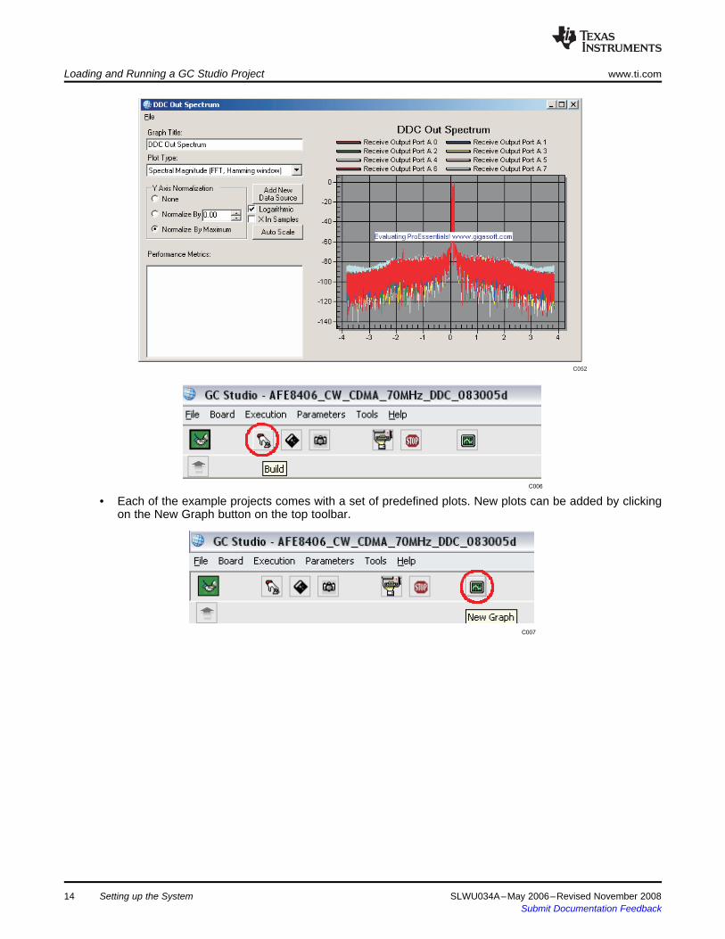
C052
C006
C007
Loading and Running a GC Studio Project www.ti.com
• Each of the example projects comes with a set of predefined plots. New plots can be added by clickingon the New Graph button on the top toolbar.
14 Setting up the System SLWU034A–May 2006–Revised November 2008Submit Documentation Feedback
C008
3.3 Creating a New GC Studio Project
www.ti.com Creating a New GC Studio Project
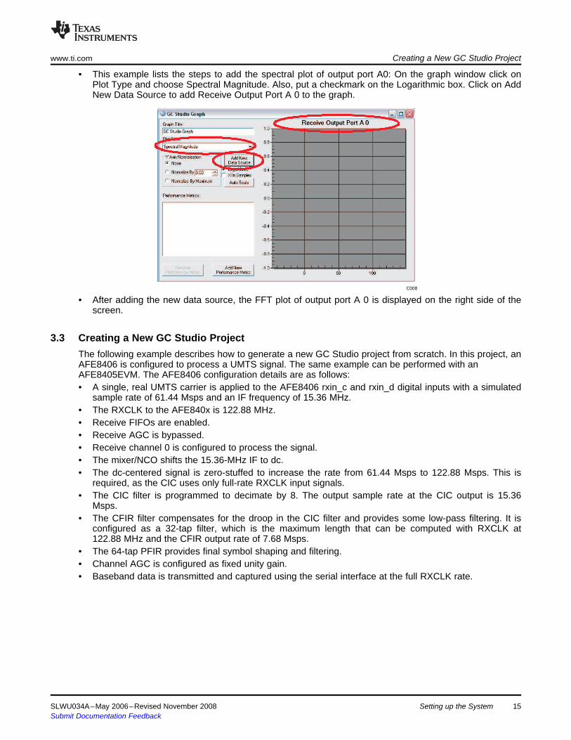
• This example lists the steps to add the spectral plot of output port A0: On the graph window click onPlot Type and choose Spectral Magnitude. Also, put a checkmark on the Logarithmic box. Click on AddNew Data Source to add Receive Output Port A 0 to the graph.
• After adding the new data source, the FFT plot of output port A 0 is displayed on the right side of thescreen.
The following example describes how to generate a new GC Studio project from scratch. In this project, anAFE8406 is configured to process a UMTS signal. The same example can be performed with anAFE8405EVM. The AFE8406 configuration details are as follows:• A single, real UMTS carrier is applied to the AFE8406 rxin_c and rxin_d digital inputs with a simulated
sample rate of 61.44 Msps and an IF frequency of 15.36 MHz.• The RXCLK to the AFE840x is 122.88 MHz.• Receive FIFOs are enabled.• Receive AGC is bypassed.• Receive channel 0 is configured to process the signal.• The mixer/NCO shifts the 15.36-MHz IF to dc.• The dc-centered signal is zero-stuffed to increase the rate from 61.44 Msps to 122.88 Msps. This is
required, as the CIC uses only full-rate RXCLK input signals.• The CIC filter is programmed to decimate by 8. The output sample rate at the CIC output is 15.36
Msps.• The CFIR filter compensates for the droop in the CIC filter and provides some low-pass filtering. It is
configured as a 32-tap filter, which is the maximum length that can be computed with RXCLK at122.88 MHz and the CFIR output rate of 7.68 Msps.
• The 64-tap PFIR provides final symbol shaping and filtering.• Channel AGC is configured as fixed unity gain.• Baseband data is transmitted and captured using the serial interface at the full RXCLK rate.
SLWU034A–May 2006–Revised November 2008 Setting up the System 15Submit Documentation Feedback
C003
C010
Creating a New GC Studio Project www.ti.com
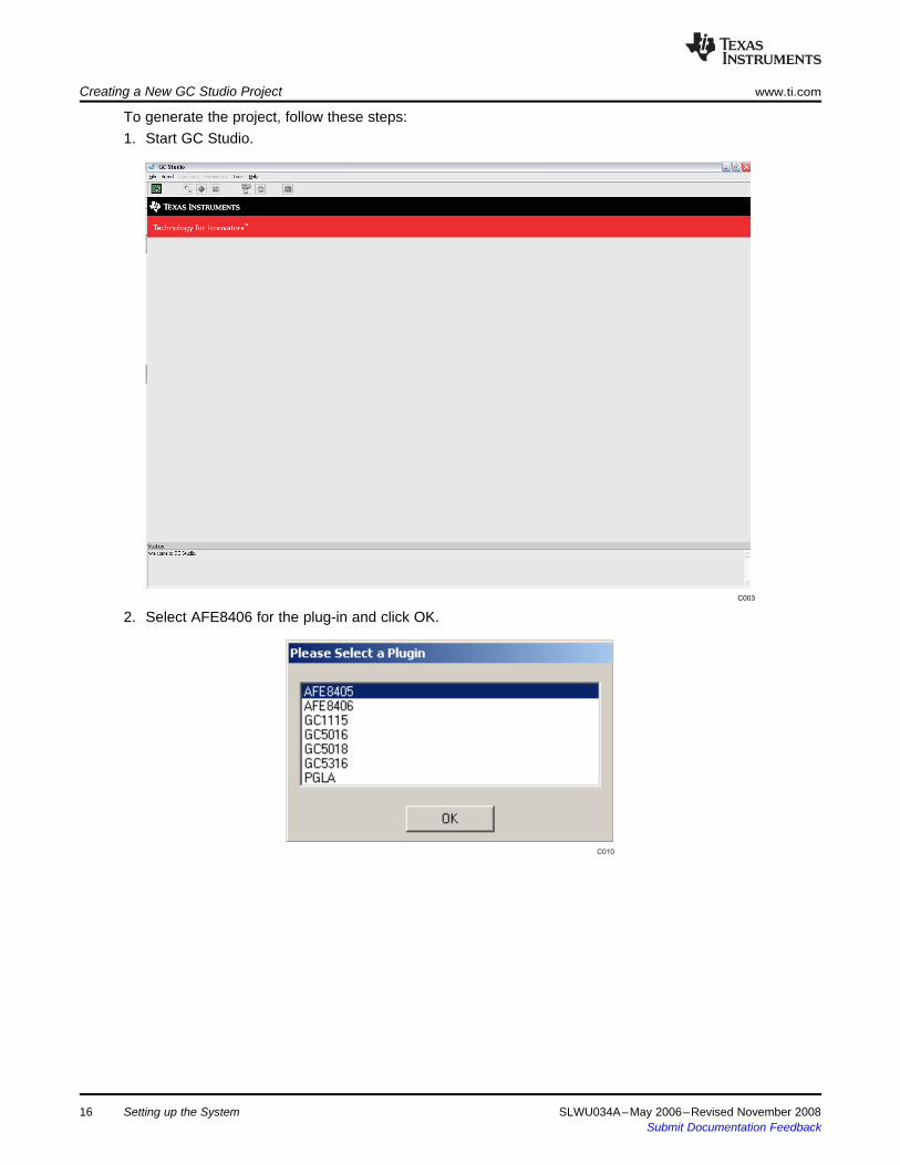
To generate the project, follow these steps:1. Start GC Studio.
2. Select AFE8406 for the plug-in and click OK.
16 Setting up the System SLWU034A–May 2006–Revised November 2008Submit Documentation Feedback
C009
C011
www.ti.com Creating a New GC Studio Project
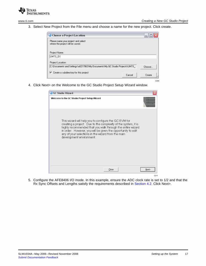
3. Select New Project from the File menu and choose a name for the new project. Click create.
4. Click Next> on the Welcome to the GC Studio Project Setup Wizard window.
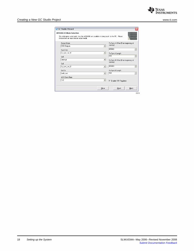
5. Configure the AFE8406 I/O mode. In this example, ensure the ADC clock rate is set to 1/2 and that theRx Sync Offsets and Lengths satisfy the requirements described in Section 4.2. Click Next>.
SLWU034A–May 2006–Revised November 2008 Setting up the System 17Submit Documentation Feedback
C013
Creating a New GC Studio Project www.ti.com
Setting up the System18 SLWU034A–May 2006–Revised November 2008Submit Documentation Feedback

C014
C053
www.ti.com Creating a New GC Studio Project
6. Set the simulated clock rate to 122.88 MHz and click Next>.
7. Click Next> on Channel Copying.8. Set the desired Stimulus and Response Memory length. Click Next>.
SLWU034A–May 2006–Revised November 2008 Setting up the System 19Submit Documentation Feedback
C016
C017
Creating a New GC Studio Project www.ti.com
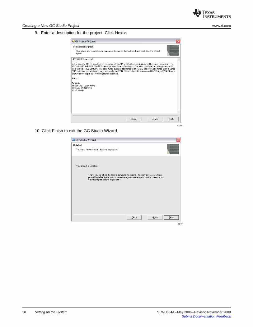
9. Enter a description for the project. Click Next>.
10. Click Finish to exit the GC Studio Wizard.
20 Setting up the System SLWU034A–May 2006–Revised November 2008Submit Documentation Feedback

C018
C019
www.ti.com Creating a New GC Studio Project
11. Click on the large AFE8406 box on the left side of the GUI to display the global control registers.
12. Double-click on the AFE8406 block to push down one level into the AFE8406. Click on the InputInterface block to display and edit the receive input interface registers. Set rate_sel to HALF; thisconfigures the AFE8406 for input samples at 1/2 the RXCLK rate. Set adc_fifo_bypass to NOTBYPASSED to enable the rxin_a/b/c/d input FIFO circuits.
SLWU034A–May 2006–Revised November 2008 Setting up the System 21Submit Documentation Feedback
C020
C021
Creating a New GC Studio Project www.ti.com
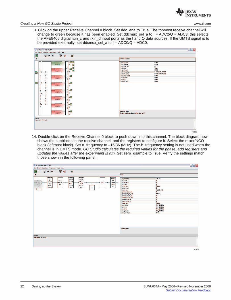
13. Click on the upper Receive Channel 0 block. Set ddc_ena to True. The topmost receive channel willchange to green because it has been enabled. Set ddcmux_sel_a to I = ADC2/Q = ADC3; this selectsthe AFE8406 digital rxin_c and rxin_d input ports as the I and Q data sources. If the UMTS signal is tobe provided externally, set ddcmux_sel_a to I = ADC0/Q = ADC0.
14. Double-click on the Receive Channel 0 block to push down into this channel. The block diagram nowshows the subblocks in the receive channel, and the registers to configure it. Select the mixer/NCOblock (leftmost block). Set a_frequency to –15.36 (MHz). The b_frequency setting is not used when thechannel is in UMTS mode. GC Studio calculates the required values for the phase_add registers andupdates the values after the experiment is run. Set zero_qsample to True. Verify the settings matchthose shown in the following panel.
22 Setting up the System SLWU034A–May 2006–Revised November 2008Submit Documentation Feedback
C022
C023
www.ti.com Creating a New GC Studio Project
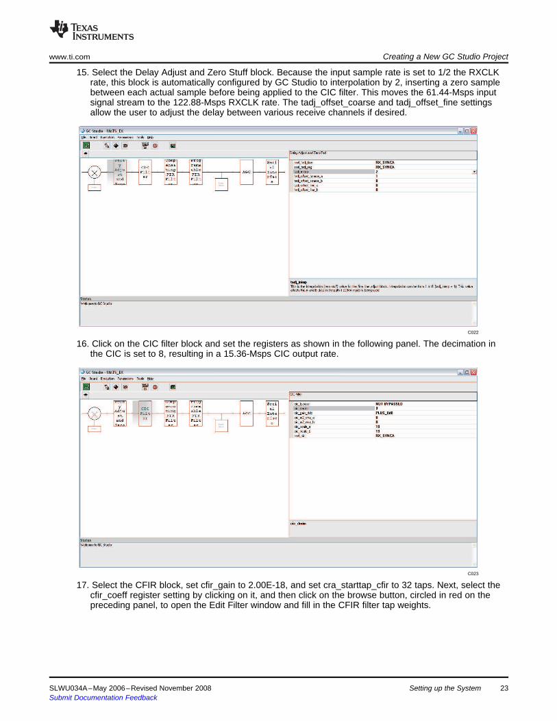
15. Select the Delay Adjust and Zero Stuff block. Because the input sample rate is set to 1/2 the RXCLKrate, this block is automatically configured by GC Studio to interpolation by 2, inserting a zero samplebetween each actual sample before being applied to the CIC filter. This moves the 61.44-Msps inputsignal stream to the 122.88-Msps RXCLK rate. The tadj_offset_coarse and tadj_offset_fine settingsallow the user to adjust the delay between various receive channels if desired.
16. Click on the CIC filter block and set the registers as shown in the following panel. The decimation inthe CIC is set to 8, resulting in a 15.36-Msps CIC output rate.
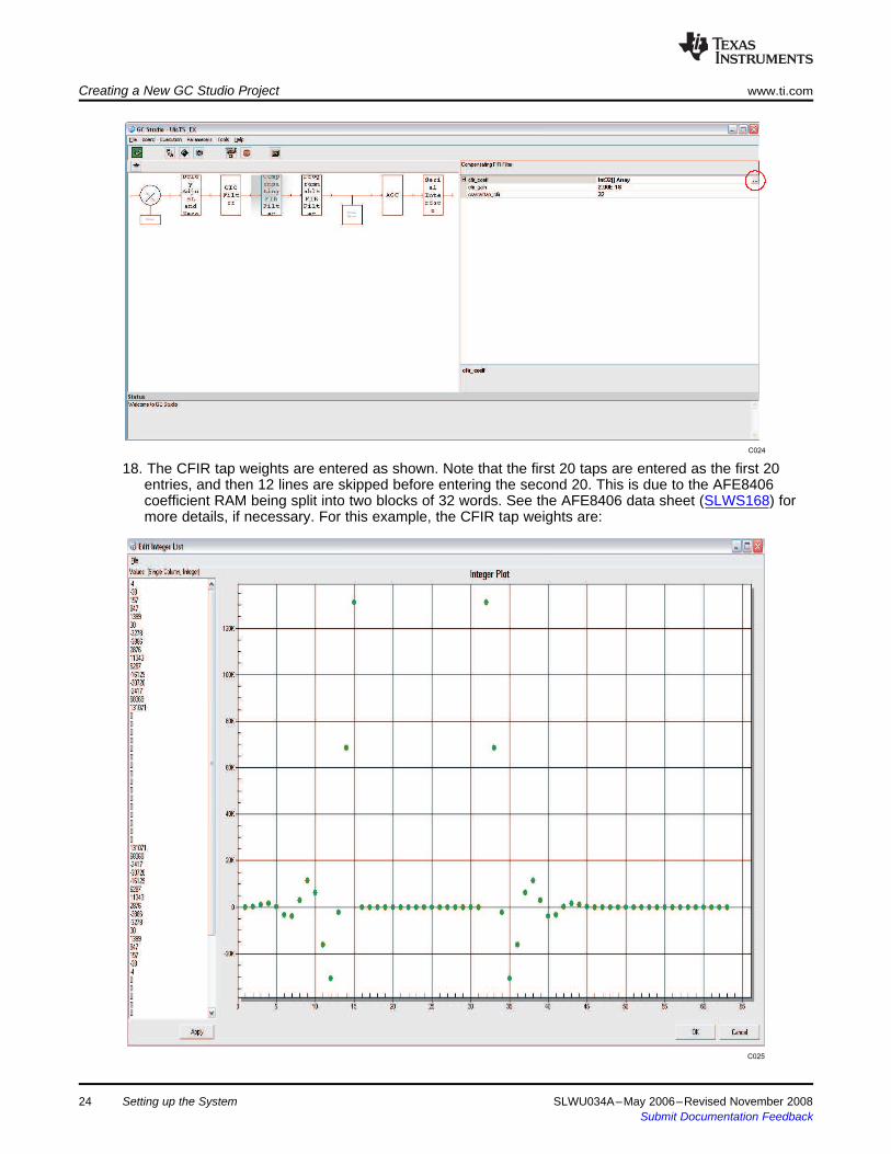
17. Select the CFIR block, set cfir_gain to 2.00E-18, and set cra_starttap_cfir to 32 taps. Next, select thecfir_coeff register setting by clicking on it, and then click on the browse button, circled in red on thepreceding panel, to open the Edit Filter window and fill in the CFIR filter tap weights.
SLWU034A–May 2006–Revised November 2008 Setting up the System 23Submit Documentation Feedback
C024
C025
Creating a New GC Studio Project www.ti.com
18. The CFIR tap weights are entered as shown. Note that the first 20 taps are entered as the first 20entries, and then 12 lines are skipped before entering the second 20. This is due to the AFE8406coefficient RAM being split into two blocks of 32 words. See the AFE8406 data sheet (SLWS168) formore details, if necessary. For this example, the CFIR tap weights are:
24 Setting up the System SLWU034A–May 2006–Revised November 2008Submit Documentation Feedback
C026
C027
www.ti.com Creating a New GC Studio Project
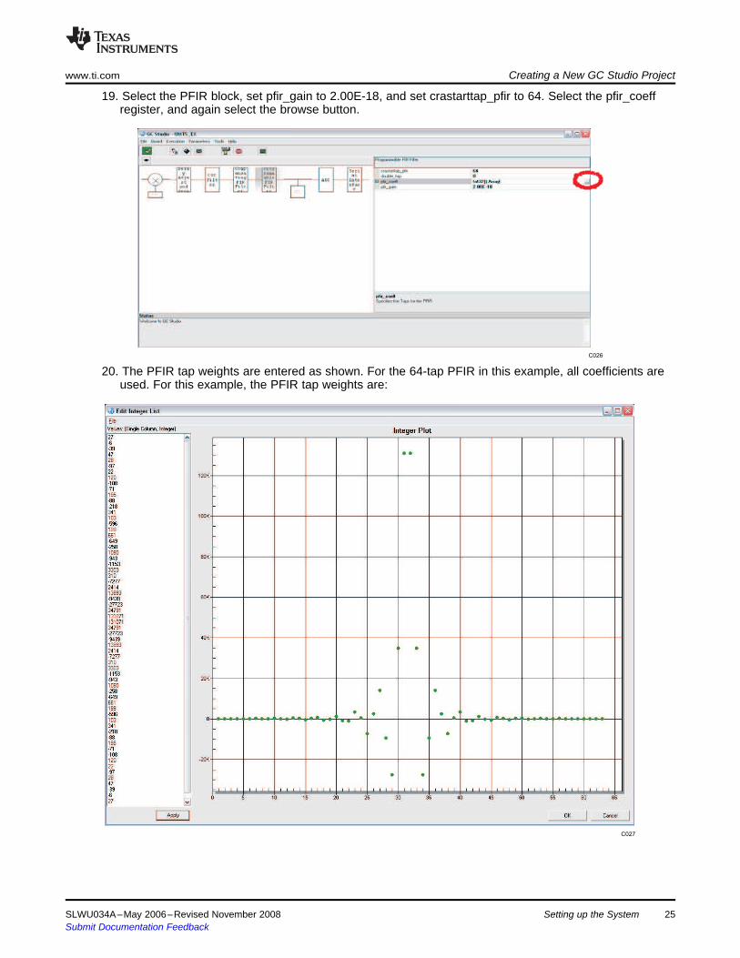
19. Select the PFIR block, set pfir_gain to 2.00E-18, and set crastarttap_pfir to 64. Select the pfir_coeffregister, and again select the browse button.
20. The PFIR tap weights are entered as shown. For the 64-tap PFIR in this example, all coefficients areused. For this example, the PFIR tap weights are:
SLWU034A–May 2006–Revised November 2008 Setting up the System 25Submit Documentation Feedback
C028
C029
Creating a New GC Studio Project www.ti.com
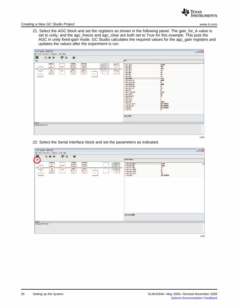
21. Select the AGC block and set the registers as shown in the following panel. The gain_for_A value isset to unity, and the agc_freeze and agc_clear are both set to True for this example. This puts theAGC in unity fixed-gain mode. GC Studio calculates the required values for the agc_gain registers andupdates the values after the experiment is run.
22. Select the Serial Interface block and set the parameters as indicated.
26 Setting up the System SLWU034A–May 2006–Revised November 2008Submit Documentation Feedback
C030
www.ti.com Creating a New GC Studio Project
23. After verifying the values for the serial interface, click the arrow circled in red in the preceding panel topop up one level in the AFE8406 hierarchy.Through the preceding steps, receive channel 0 has now been configured as follows:• UMTS input signal at 61.44 Msps with a 15.36-MHz IF• Mixer/NCO block shifts the signal to dc.• Zero-stuff block interpolates by 2, moving the 61.44-Msps signal to 122.88 Msps.• CIC block decimates by 8, to 15.36 Msps.• 32-tap CFIR compensates for the CIC droop, filters and decimates the signal to 7.68 Msps.• 64-tap PFIR filters the signal.• Channel AGC is set to a fixed gain of 1.• Serial interface is used to output the baseband signal.AThe AFE8406 daughtercard configuration uses rx_sync_out_6 as the strobe that indicates when theserial output data starts each transfer. In the following step, the receive channel-0 configuration iscopied to receive channel 6 so the strobe is present in the captured GC101 data.
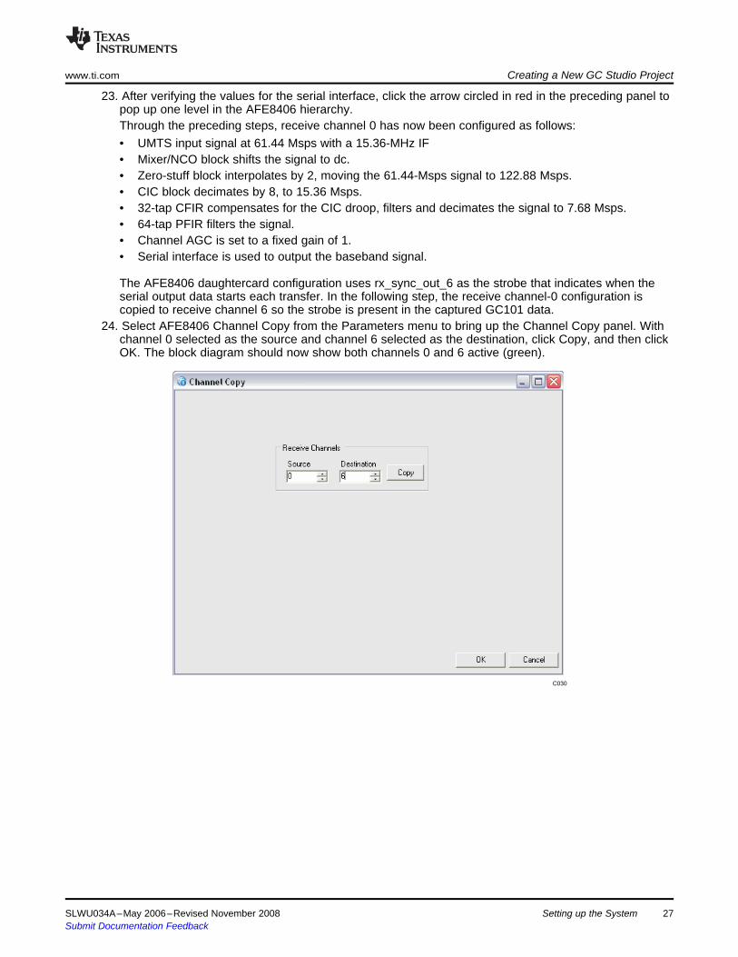
24. Select AFE8406 Channel Copy from the Parameters menu to bring up the Channel Copy panel. Withchannel 0 selected as the source and channel 6 selected as the destination, click Copy, and then clickOK. The block diagram should now show both channels 0 and 6 active (green).
SLWU034A–May 2006–Revised November 2008 Setting up the System 27Submit Documentation Feedback
C031
C032
Creating a New GC Studio Project www.ti.com
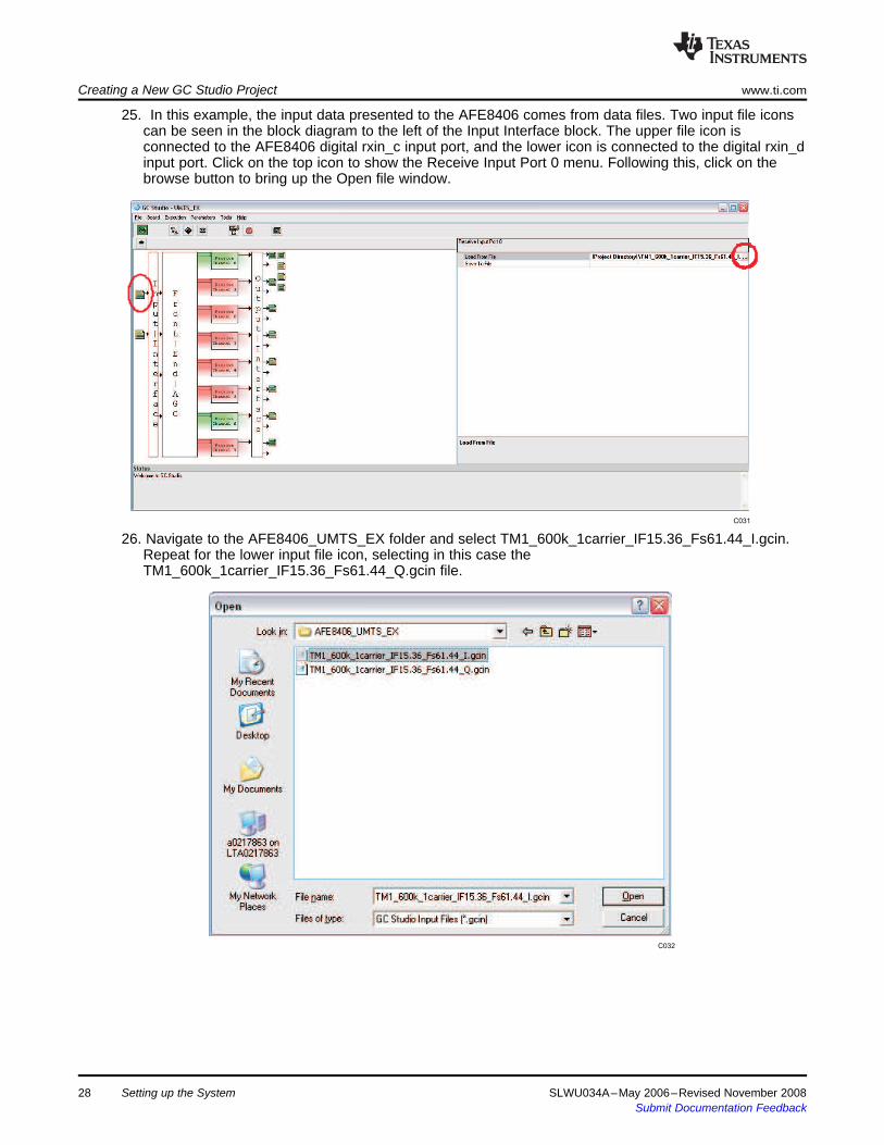
25. In this example, the input data presented to the AFE8406 comes from data files. Two input file iconscan be seen in the block diagram to the left of the Input Interface block. The upper file icon isconnected to the AFE8406 digital rxin_c input port, and the lower icon is connected to the digital rxin_dinput port. Click on the top icon to show the Receive Input Port 0 menu. Following this, click on thebrowse button to bring up the Open file window.
26. Navigate to the AFE8406_UMTS_EX folder and select TM1_600k_1carrier_IF15.36_Fs61.44_I.gcin.Repeat for the lower input file icon, selecting in this case theTM1_600k_1carrier_IF15.36_Fs61.44_Q.gcin file.
28 Setting up the System SLWU034A–May 2006–Revised November 2008Submit Documentation Feedback

C033
C034
www.ti.com Creating a New GC Studio Project
27. Click on the graph button, circled in red, to open the graph panel.
28. Click the Add New Data Source button and select Receive Output Port A 0.
SLWU034A–May 2006–Revised November 2008 Setting up the System 29Submit Documentation Feedback
C035
C036
Creating a New GC Studio Project www.ti.com
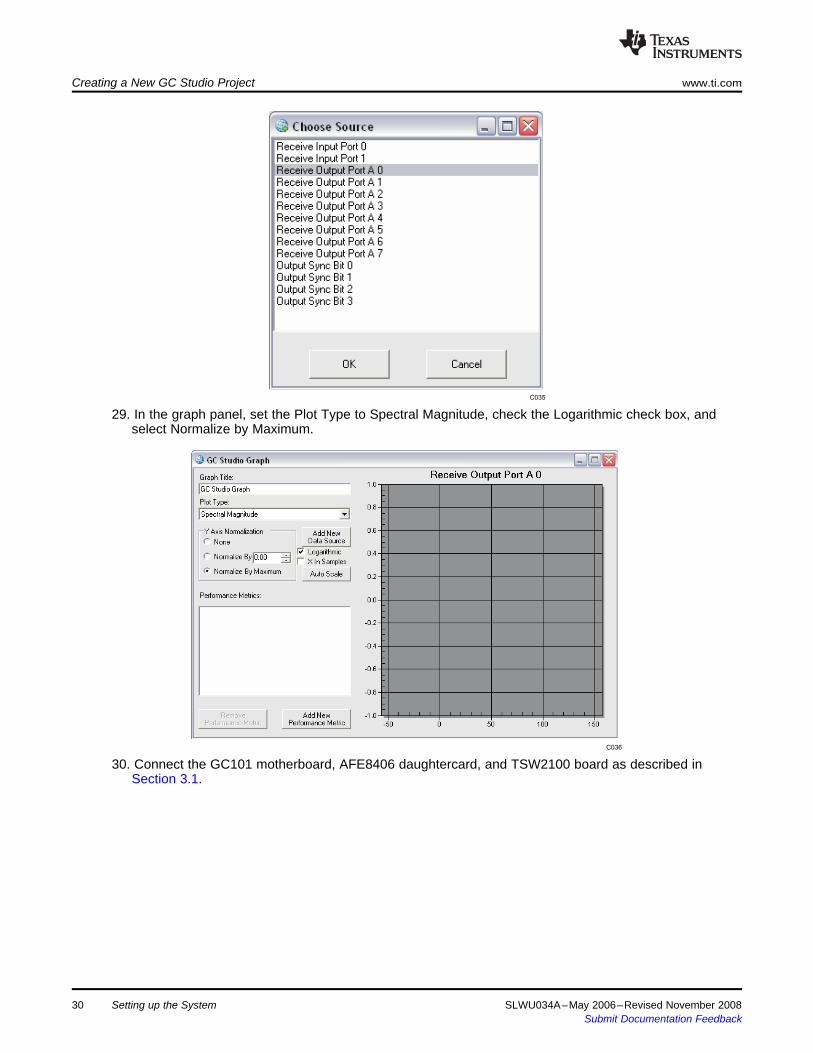
29. In the graph panel, set the Plot Type to Spectral Magnitude, check the Logarithmic check box, andselect Normalize by Maximum.
30. Connect the GC101 motherboard, AFE8406 daughtercard, and TSW2100 board as described inSection 3.1.
30 Setting up the System SLWU034A–May 2006–Revised November 2008Submit Documentation Feedback
C047
C051
C037
www.ti.com Creating a New GC Studio Project
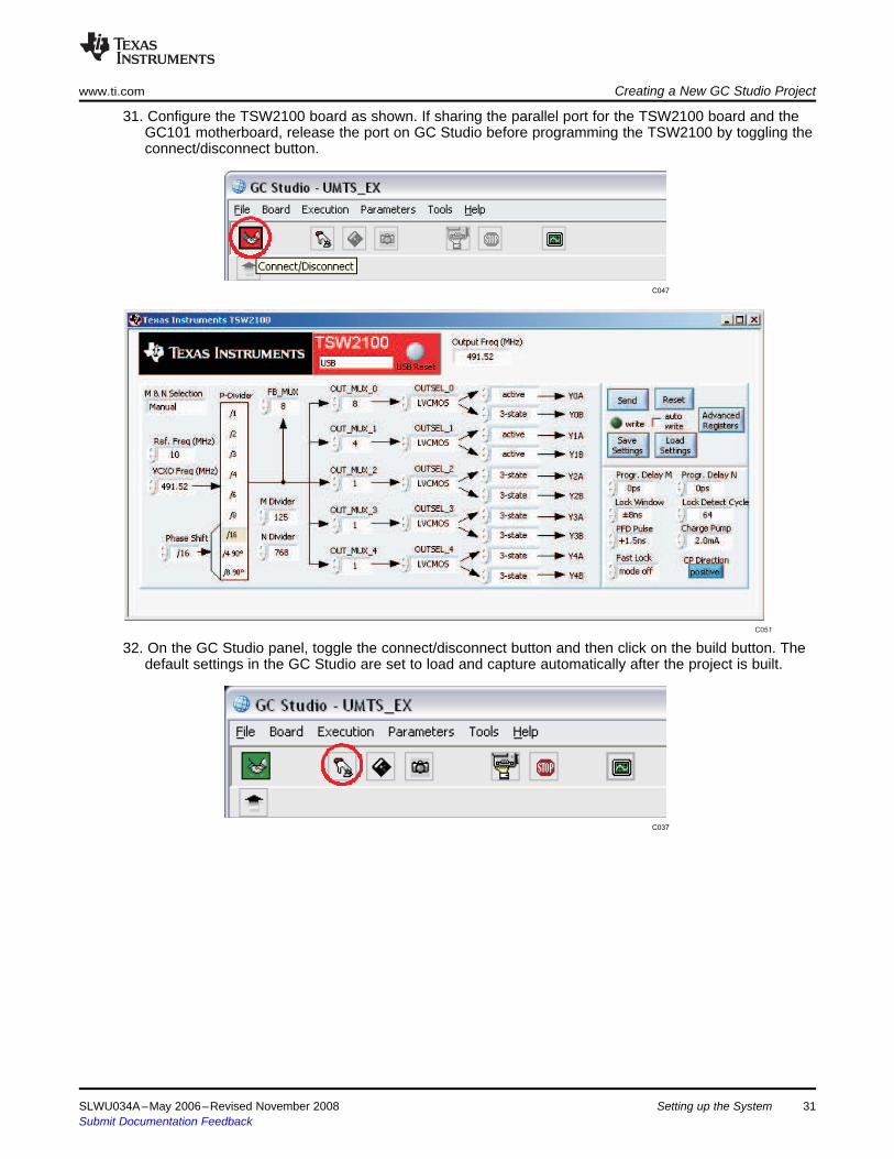
31. Configure the TSW2100 board as shown. If sharing the parallel port for the TSW2100 board and theGC101 motherboard, release the port on GC Studio before programming the TSW2100 by toggling theconnect/disconnect button.
32. On the GC Studio panel, toggle the connect/disconnect button and then click on the build button. Thedefault settings in the GC Studio are set to load and capture automatically after the project is built.
SLWU034A–May 2006–Revised November 2008 Setting up the System 31Submit Documentation Feedback
C038
Creating a New GC Studio Project www.ti.com
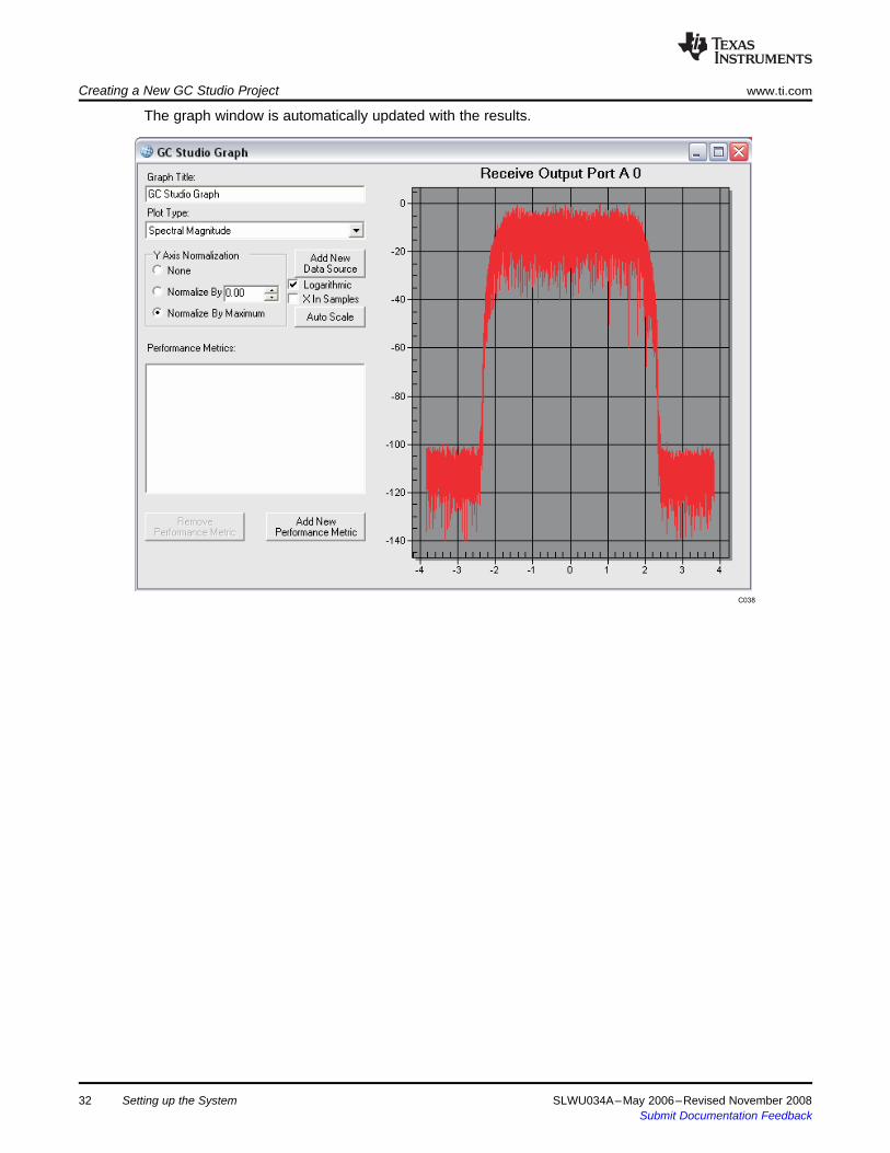
The graph window is automatically updated with the results.
Setting up the System32 SLWU034A–May 2006–Revised November 2008Submit Documentation Feedback
4.1 Saving the Output to a File
C039
Chapter 4SLWU034A–May 2006–Revised November 2008
Other Options in GC Studio
GC Studio offers much flexibility in evaluating the data processed by the AFE840x. Following is a list ofsome of these capabilities:
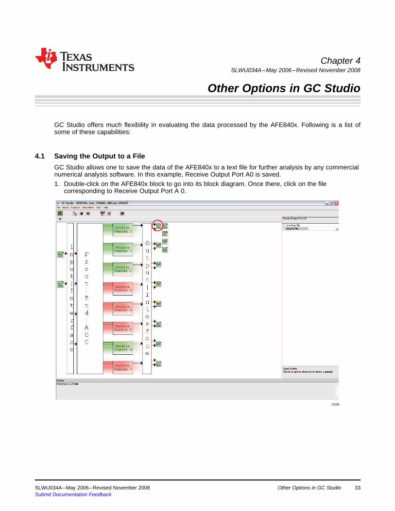
GC Studio allows one to save the data of the AFE840x to a text file for further analysis by any commercialnumerical analysis software. In this example, Receive Output Port A0 is saved.1. Double-click on the AFE840x block to go into its block diagram. Once there, click on the file
corresponding to Receive Output Port A 0.
SLWU034A–May 2006–Revised November 2008 Other Options in GC Studio 33Submit Documentation Feedback
C040
4.2 Changing the Data Capture Size
C041
Changing the Data Capture Size www.ti.com
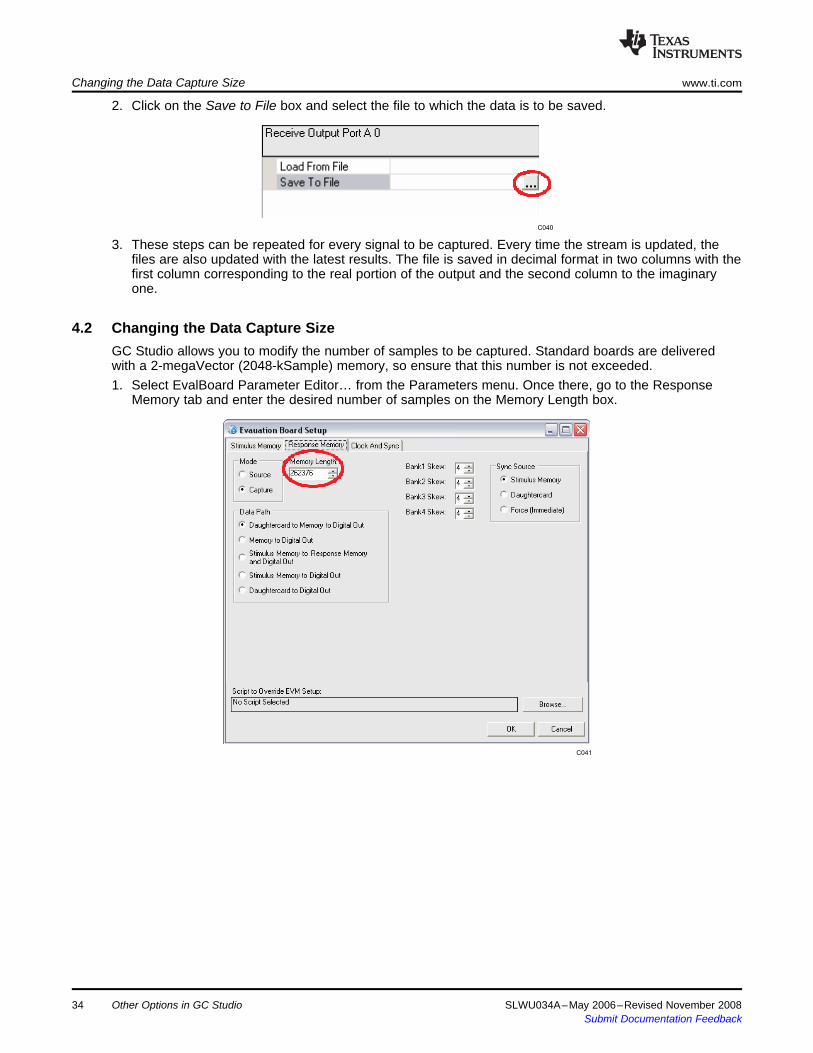
2. Click on the Save to File box and select the file to which the data is to be saved.
3. These steps can be repeated for every signal to be captured. Every time the stream is updated, thefiles are also updated with the latest results. The file is saved in decimal format in two columns with thefirst column corresponding to the real portion of the output and the second column to the imaginaryone.
GC Studio allows you to modify the number of samples to be captured. Standard boards are deliveredwith a 2-megaVector (2048-kSample) memory, so ensure that this number is not exceeded.1. Select EvalBoard Parameter Editor… from the Parameters menu. Once there, go to the Response
Memory tab and enter the desired number of samples on the Memory Length box.
34 Other Options in GC Studio SLWU034A–May 2006–Revised November 2008Submit Documentation Feedback

T0124-01
Stimulus memory
Sync length
Sync offset
Captured data is in this region
C042
www.ti.com Changing the Data Capture Size
2. In the current version of GC Studio, the Response Memory capture is triggered by the StimulusMemory. Improper setting of the Stimulus Memory may result in errors in the captured data. Becauseof this, every time the captured data size is modified, it is necessary to corroborate that the StimulusMemory size and the Sync Offset are set up properly.
3. From the foregoing diagram, it is observed that the Sync Offset must be slightly bigger than theResponse Memory size. Also, it is necessary to verify that the Stimulus Memory size is large enough toencompass the Sync Offset and the Sync Length. To adjust the Stimulus Memory size, selectEvalBoard Parameter Editor… from the Parameters menu and go to the Stimulus Memory tab. Enterthe proper number of samples in the Memory Length box.
SLWU034A–May 2006–Revised November 2008 Other Options in GC Studio 35Submit Documentation Feedback
C043
4.3 Capturing the AFE840x Test Bus Output
Capturing the AFE840x Test Bus Output www.ti.com
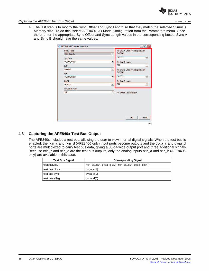
4. The last step is to modify the Sync Offset and Sync Length so that they match the selected StimulusMemory size. To do this, select AFE840x I/O Mode Configuration from the Parameters menu. Oncethere, enter the appropriate Sync Offset and Sync Length values in the corresponding boxes. Sync Aand Sync B should have the same values.
The AFE840x includes a test bus, allowing the user to view internal digital signals. When the test bus isenabled, the rxin_c and rxin_d (AFE8406 only) input ports become outputs and the dvga_c and dvga_dports are multiplexed to carry test bus data, giving a 36-bit-wide output port and three additional signals.Because rxin_c and rxin_d are the test bus outputs, only the analog inputs rxin_a and rxin_b (AFE8406only) are available in this case.
Test Bus Signal Corresponding Signaltestbus(35:0) rxin_d(15:0), dvga_c(3:2), rxin_c(15:0), dvga_c(5:4)test bus clock dvga_c(1)test bus sync dvga_c(0)test bus aflag dvga_d(5)
Other Options in GC Studio36 SLWU034A–May 2006–Revised November 2008Submit Documentation Feedback
C044
www.ti.com Capturing the AFE840x Test Bus Output
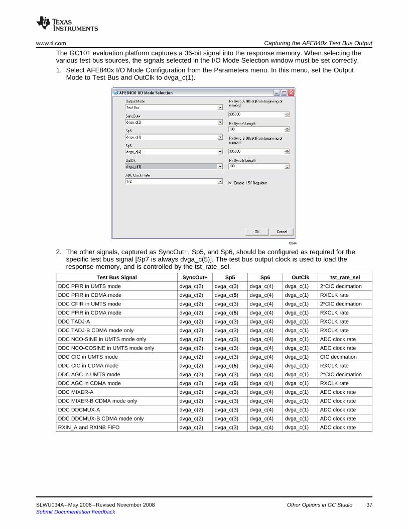
The GC101 evaluation platform captures a 36-bit signal into the response memory. When selecting thevarious test bus sources, the signals selected in the I/O Mode Selection window must be set correctly.1. Select AFE840x I/O Mode Configuration from the Parameters menu. In this menu, set the Output
Mode to Test Bus and OutClk to dvga_c(1).
2. The other signals, captured as SyncOut+, Sp5, and Sp6, should be configured as required for thespecific test bus signal [Sp7 is always dvga_c(5)]. The test bus output clock is used to load theresponse memory, and is controlled by the tst_rate_sel.
Test Bus Signal SyncOut+ Sp5 Sp6 OutClk tst_rate_selDDC PFIR in UMTS mode dvga_c(2) dvga_c(3) dvga_c(4) dvga_c(1) 2*CIC decimationDDC PFIR in CDMA mode dvga_c(2) dvga_c(5) dvga_c(4) dvga_c(1) RXCLK rateDDC CFIR in UMTS mode dvga_c(2) dvga_c(3) dvga_c(4) dvga_c(1) 2*CIC decimationDDC PFIR in CDMA mode dvga_c(2) dvga_c(5) dvga_c(4) dvga_c(1) RXCLK rateDDC TADJ-A dvga_c(2) dvga_c(3) dvga_c(4) dvga_c(1) RXCLK rateDDC TADJ-B CDMA mode only dvga_c(2) dvga_c(3) dvga_c(4) dvga_c(1) RXCLK rateDDC NCO-SINE in UMTS mode only dvga_c(2) dvga_c(3) dvga_c(4) dvga_c(1) ADC clock rateDDC NCO-COSINE in UMTS mode only dvga_c(2) dvga_c(3) dvga_c(4) dvga_c(1) ADC clock rateDDC CIC in UMTS mode dvga_c(2) dvga_c(3) dvga_c(4) dvga_c(1) CIC decimationDDC CIC in CDMA mode dvga_c(2) dvga_c(5) dvga_c(4) dvga_c(1) RXCLK rateDDC AGC in UMTS mode dvga_c(2) dvga_c(3) dvga_c(4) dvga_c(1) 2*CIC decimationDDC AGC in CDMA mode dvga_c(2) dvga_c(5) dvga_c(4) dvga_c(1) RXCLK rateDDC MIXER-A dvga_c(2) dvga_c(3) dvga_c(4) dvga_c(1) ADC clock rateDDC MIXER-B CDMA mode only dvga_c(2) dvga_c(3) dvga_c(4) dvga_c(1) ADC clock rateDDC DDCMUX-A dvga_c(2) dvga_c(3) dvga_c(4) dvga_c(1) ADC clock rateDDC DDCMUX-B CDMA mode only dvga_c(2) dvga_c(3) dvga_c(4) dvga_c(1) ADC clock rateRXIN_A and RXINB FIFO dvga_c(2) dvga_c(3) dvga_c(4) dvga_c(1) ADC clock rate
SLWU034A–May 2006–Revised November 2008 Other Options in GC Studio 37Submit Documentation Feedback
C045
Capturing the AFE840x Test Bus Output www.ti.com
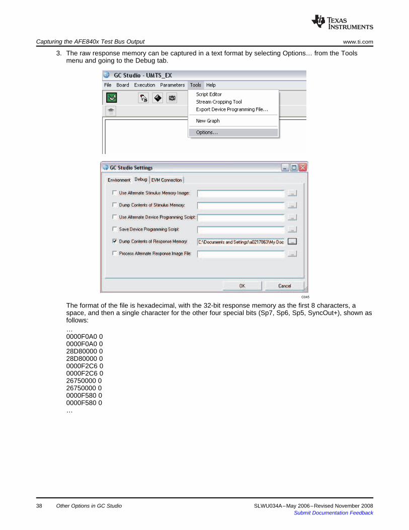
3. The raw response memory can be captured in a text format by selecting Options… from the Toolsmenu and going to the Debug tab.
The format of the file is hexadecimal, with the 32-bit response memory as the first 8 characters, aspace, and then a single character for the other four special bits (Sp7, Sp6, Sp5, SyncOut+), shown asfollows:…0000F0A0 00000F0A0 028D80000 028D80000 00000F2C6 00000F2C6 026750000 026750000 00000F580 00000F580 0…A
38 Other Options in GC Studio SLWU034A–May 2006–Revised November 2008Submit Documentation Feedback
C046
www.ti.com Capturing the AFE840x Test Bus Output
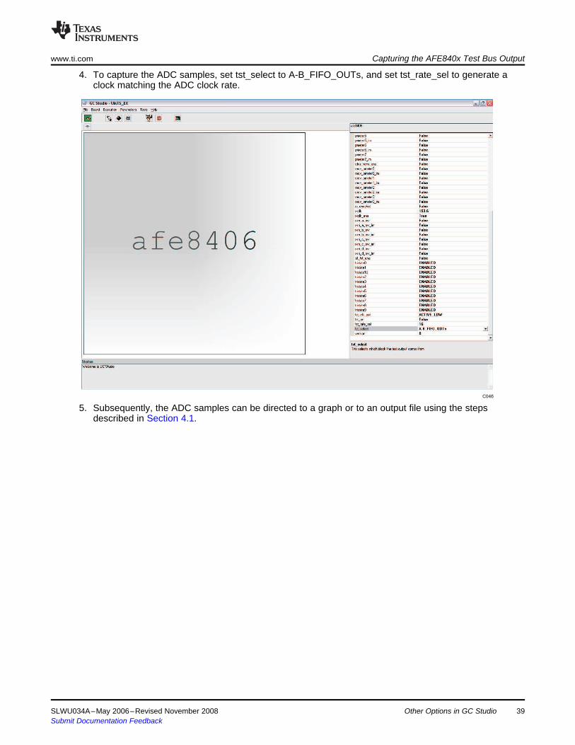
4. To capture the ADC samples, set tst_select to A-B_FIFO_OUTs, and set tst_rate_sel to generate aclock matching the ADC clock rate.
5. Subsequently, the ADC samples can be directed to a graph or to an output file using the stepsdescribed in Section 4.1.
SLWU034A–May 2006–Revised November 2008 Other Options in GC Studio 39Submit Documentation Feedback

Other Options in GC Studio40 SLWU034A–May 2006–Revised November 2008Submit Documentation Feedback
B0134-01
CLK+
SP3
adcclk_c
To/From GC101 SWITCH
External power supply
rx_synca
SIGIN[31:16]
SIGIN[15:0]
rxin_c_ovr
SIGOUT[15:0]
rxclk_out
SYNCOUT+
GC101 GC101
From GC101 To GC101
AFE8406 DIMM board
SP1
SYNC+
SP2
CLKOUT+
dvga_c[5]
dvga_c[4]
dvga_c[3]
dvga_c[2]
SP5
SP6
SP7
rx_sync_out
interrupt
SIGOUT[31:16]rxout_7:3_d:a
adcclk_d
rxout_4:0_d:a
[dvga_c[3:0]:dvga_a[5:0]:
dvga_b[5:0]]
rx_sync_out_6
dvga_c[0]
dvga_d[5]
dvga_c[1]
rxin_d_ovr
rx_sync_out_0
rxin_c[15:0]
rxin_d[15:0]
rx_syncb
AFE8406
Tristate buffercontrol register
TTJTAGMPU Interface[a(6), d(16), rd_n,wr_n, ce_n,reset_n],Power/Gnd
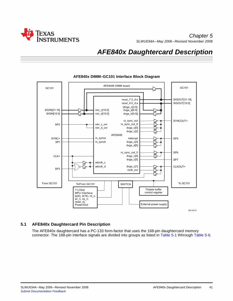
5.1 AFE840x Daughtercard Pin Description
Chapter 5SLWU034A–May 2006–Revised November 2008
AFE840x Daughtercard Description
AFE840x DIMM–GC101 Interface Block Diagram
The AFE840x daughtercard has a PC-133 form-factor that uses the 168-pin daughtercard memoryconnector. The 168-pin interface signals are divided into groups as listed in Table 5-1 thhrough Table 5-6.
SLWU034A–May 2006–Revised November 2008 AFE840x Daughtercard Description 41Submit Documentation Feedback
AFE840x Daughtercard Pin Description www.ti.com
Table 5-1. Memory Input Bus—36 Data Inputs Used to Stimulate the AFE840x InputsSignal Alias Description
SIGIN(35) SP3 Clock gating signal for adcclk_a and adcclk_bSIGIN(34) SP2 rxin_c_ovr and rxin_d_ovr input signalsSIGIN(33) SP1 rx_syncb input signalSIGIN(32) SYNC+ rx_synca input signalSIGIN(31:16) rxin_c(15:0) input dataSIGIN(15:0) rxin_d(15:0) input data
Table 5-2. Memory Output Bus—36 Data Outputs From Selected AFE840x Outputs Captured by theGC101
Signal Alias DescriptionSIGOUT(35) SP7 dvga_c(5)SIGOUT(34) SP6 dvga_c(4) or rx_sync_out_0SIGOUT(33) SP5 dvga_c(3), dvga_d(5) or interruptSIGOUT(32) SYNCOUT+ rx_sync_out, rx_sync_out_6, dvga_c(0) or dvga_c(2)SIGOUT(31:16) rxout_7:4_d:a baseband DDC data or rxin_d(15:0) testbus outputSIGOUT(15:0) rxout_3:0_d:a baseband DDC data or rxin_c(15:0) testbus output
Table 5-3. ClockSignal Description
CLK+ RXCLK clock for AFE840x; can be used as a full-rate or gated clock source when combinedwith the gating signal SP3 for the adcclk_a and adcclk_b (AFE8406 only) inputs.
CLKOUT Clock signal from the daughtercard to the GC101; RXCLK, rxclk_out from the GC5018 ordvga_c(1)
Table 5-4. Microprocessor Control Bus—Bus to Program the Internal RegistersSignal Description
d(15:0) Control data I//O bus, active-high bidirectional I/O pins. This is the 16-bit control data I/Obus. Control registers are written to or read from through these pins. The chip drives thesepins when CE is low, RD is low, and WR is high.
A(10:0) Control address bus, active-high inputs. These pins are used to address the control registerswithin the chip. Each of the control register within the chip is assigned a unique address. Acontrol retister can be written to or read from by having the page register set to theappropriate page and then setting A(10:0) to the register address.
CE, RD, WR, and RST ce_n, rd_n, wr_n and rst_n on the AFE840x
Table 5-5. JTAGSignal Description
JTAG 5-pin JTAG test port for AFE840xTRST, TCK, TMS, TDI, TDO trst_n, tck, tms, tdi, and tdo on the AFE840x
Table 5-6. Power and GroundSignal Description
VDUT1 3.3-V power from GC101 EVM to the daughtercardGND Return path for the daughtercard
See the GC101 EVM User's Guide (SLWU018) for the 168-pin connector table. Detailed Schematics andBill of Materials (BOM) for the AFE840x daughtercard can be found on the provide CD .
AFE840x Daughtercard Description42 SLWU034A–May 2006–Revised November 2008Submit Documentation Feedback

5.2 AFE840x Daughtercard Jumpers
5.3 AFE840x Daughtercard Power Supplies
5.4 AFE840x Daughtercard Clock Configurations
www.ti.com AFE840x Daughtercard Jumpers
The following table describes the various jumpers on the AFE840x daughtercard card:Jumper (Rev E Description
and older)W2 (J7) Pin_configure signal. Factory test only. Connect to VDD, pins 2-3 (default).W3 (J8) Enables ADC A outputs. Jumper installed between pins 1-2 (default). Disables ADC A outputs when jumper is
installed between pins 2-3.W4 (J9) Enables ADC B outputs (AFE8406 only) when jumper is installed between pins 1-2 (default). Disables ADC
outputs when jumper is installed between pins 2-3.W12 (J11) Clock doubler power down for the CDC5801. Jumper installed between pins 1-2 for 3.3 V, enabled (default).
Position 2-3 for 0 V, powered down.W13 (J12) 1× or 2× clock select for the CDC5801. Jumper installed between 2-3 for 2× output clock (default). Position
1-2 for 2× output clock.W7 (W14) 3.3-V fuse power for ADC. Jumper installed between pins 1-2 for 3.3 V, normal operation (default). Position
2-3 for 0 V – DO NOT USE THIS POSITION.W10 (W15) 3.3-V fuse power for DDC. Jumper installed between pins 1-2 for 3.3 V, normal operation (default). Position
2-3 for 0 V – DO NOT USE THIS POSITION.W9 (J17) SDI - Set to AVDD.Factory use only, jumper removed (default). SEN - ADC internal reference when set to
GND. Jumper installed between pins 3-4 (default). Ext reference with jumper removed. SCLK - AVDD forAFE8405, jumper removed 9default). Power down for AFE8406, jumper installed between Pins 5-6 (default).
N/A (W13) External DVDD power supply. Jumper installed betwwen pins 1-2 for internal 1.5 V to DVDD (default).Position 2-3 for external 1.5 V through J24.
W8 (W25) External AVDD power supply. Jumper installed between pins 1-2 for internal 3.3 V to AVDD (default). Position2-3 for external 3.3 V through J29.
W11 (W26) External VDDS power supply. Jumper installed between pins 1-2 for internal 3.3 V to VDDS (default). Position2-3 for external 3.3 V through J30.
W5 (W27) External DRVDD power supply. Jumper installed between pins 1-2 for internal 3.3 V to DRVDD(default).Position 2-3 for external 3.3 V through J28.
W6 (J23) 1.5-V regulator software control using c10 register bit – DO NOT INSTALL.
The AFE840x I/O and core power supplies are 3.3 V and 1.5 V, respectively. The default configuration ofthe AFE840x daughtercard enables the GC101 motherboard to supply 3.3 V to the daughtercard, whichincludes a 1.5-V regulator. Alternatively, by modifying jumpers W13, W25, W26 and W27, on Rev E orolder boards, and W5, W8, and W11, on Rev F or newer boards, external power supplies can be used toprovide these voltages to the daughtercard.
The AFE840x daughtercard card allows for the following clock configurations:1. Default configuration (to be used with TSW2100): AFE840x daughtercard RX clock SMA input
• Input RX clock rate at J5 (CLKM)• Install 0-Ω resistors in
– R40– R72– R58
• Remove resistors in– R36– R43– R52– R73
• For CDCF5801 at 1, install– J12 jumper between pins 2 and 3
SLWU034A–May 2006–Revised November 2008 AFE840x Daughtercard Description 43Submit Documentation Feedback
AFE840x Daughtercard Clock Configurations www.ti.com
• For CDCF5801 at 2, install– J12 jumper between pins 1 and 2
• Clock path:J5 → R40 → R72 → C137 → U22 (pin2) → U22 (pin20) → R58 → AFE8406 (ball r22)
2. Configuration for AFE840x daughtercard RX clock from GC101 (through CDCF5801)• Install 0-Ω resistors in
– R46– R70– R73– R58
• Remove resistors in– R36– R43– R52– R72
• For CDCF5801 at 1, install– J12 jumper between pins 2 and 3
• For CDCF5801 at 2, install– J12 jumper between pins 1 and 2
• Clock path:J16A (pin 34) → R46 → C148 → U2 (pin1) → U2 (pin2) → R70 →R73 → C137 → U22 (pin2) →U22 (pin20) → R58 → AFE840x (ball r22)
3. Configuration for AFE840x daughtercard RX clock from GC101 (bypass CDCF5801)• Install 0-Ω resistors in
– R46– R36– R73
• Remove resistors in– R43– R52– R73– R72– R58
• Clock path:J16A (pin 34) → R46 → C148 → U2 (pin1) → U2 (pin2) → R36 → AFE840x (ball r22)
4. Configuration for AFE8406 daughtercard RX clock from ADC clock (GC101 separate)• Install 0-Ω resistors in
– R52– R58
• Remove resistors in– R36– R43– R52– R72– R73
• For CDCF5801 at 1, install– J12 jumper between pins 2 and 3
• For CDCF5801 at 2, install– J12 jumper between pins 1 and 2
• Clock path:J6 (CLKP) → R52 → C137 → U22 (pin2) → U22 (pin20) → R58 → AFE840x (ball r22)
44 AFE840x Daughtercard Description SLWU034A–May 2006–Revised November 2008Submit Documentation Feedback

EVALUATION BOARD/KIT IMPORTANT NOTICETexas Instruments (TI) provides the enclosed product(s) under the following conditions:This evaluation board/kit is intended for use for ENGINEERING DEVELOPMENT, DEMONSTRATION, OR EVALUATION PURPOSESONLY and is not considered by TI to be a finished end-product fit for general consumer use. Persons handling the product(s) must haveelectronics training and observe good engineering practice standards. As such, the goods being provided are not intended to be completein terms of required design-, marketing-, and/or manufacturing-related protective considerations, including product safety and environmentalmeasures typically found in end products that incorporate such semiconductor components or circuit boards. This evaluation board/kit doesnot fall within the scope of the European Union directives regarding electromagnetic compatibility, restricted substances (RoHS), recycling(WEEE), FCC, CE or UL, and therefore may not meet the technical requirements of these directives or other related directives.Should this evaluation board/kit not meet the specifications indicated in the User’s Guide, the board/kit may be returned within 30 days fromthe date of delivery for a full refund. THE FOREGOING WARRANTY IS THE EXCLUSIVE WARRANTY MADE BY SELLER TO BUYERAND IS IN LIEU OF ALL OTHER WARRANTIES, EXPRESSED, IMPLIED, OR STATUTORY, INCLUDING ANY WARRANTY OFMERCHANTABILITY OR FITNESS FOR ANY PARTICULAR PURPOSE.The user assumes all responsibility and liability for proper and safe handling of the goods. Further, the user indemnifies TI from all claimsarising from the handling or use of the goods. Due to the open construction of the product, it is the user’s responsibility to take any and allappropriate precautions with regard to electrostatic discharge.EXCEPT TO THE EXTENT OF THE INDEMNITY SET FORTH ABOVE, NEITHER PARTY SHALL BE LIABLE TO THE OTHER FOR ANYINDIRECT, SPECIAL, INCIDENTAL, OR CONSEQUENTIAL DAMAGES.TI currently deals with a variety of customers for products, and therefore our arrangement with the user is not exclusive.TI assumes no liability for applications assistance, customer product design, software performance, or infringement of patents orservices described herein.Please read the User’s Guide and, specifically, the Warnings and Restrictions notice in the User’s Guide prior to handling the product. Thisnotice contains important safety information about temperatures and voltages. For additional information on TI’s environmental and/orsafety programs, please contact the TI application engineer or visit www.ti.com/esh.No license is granted under any patent right or other intellectual property right of TI covering or relating to any machine, process, orcombination in which such TI products or services might be or are used.
FCC WarningThis evaluation board/kit is intended for use for ENGINEERING DEVELOPMENT, DEMONSTRATION, OR EVALUATION PURPOSESONLY and is not considered by TI to be a finished end-product fit for general consumer use. It generates, uses, and can radiate radiofrequency energy and has not been tested for compliance with the limits of computing devices pursuant to part 15 of FCC rules, which aredesigned to provide reasonable protection against radio frequency interference. Operation of this equipment in other environments maycause interference with radio communications, in which case the user at his own expense will be required to take whatever measures maybe required to correct this interference.
Mailing Address: Texas Instruments, Post Office Box 655303, Dallas, Texas 75265Copyright © 2006, Texas Instruments Incorporated
EVM WARNINGS AND RESTRICTIONSIt is important to operate this EVM within the AVDD voltage range of –0.3 V to 3.8 V and the DVDD voltage range of –0.3 V to 5 V.Exceeding the specified input range may cause unexpected operation and/or irreversible damage to the EVM. If there are questionsconcerning the input range, please contact a TI field representative prior to connecting the input power.Applying loads outside of the specified output range may result in unintended operation and/or possible permanent damage to the EVM.Please consult the EVM User's Guide prior to connecting any load to the EVM output. If there is uncertainty as to the load specification,please contact a TI field representative.During normal operation, some circuit components may have case temperatures greater than 25°C. The EVM is designed to operateproperly with certain components above 50°C as long as the input and output ranges are maintained. These components include but arenot limited to linear regulators, switching transistors, pass transistors, and current sense resistors. These types of devices can be identifiedusing the EVM schematic located in the EVM User's Guide. When placing measurement probes near these devices during operation,please be aware that these devices may be very warm to the touch.
Mailing Address: Texas Instruments, Post Office Box 655303, Dallas, Texas 75265Copyright © 2006, Texas Instruments Incorporated

IMPORTANT NOTICETexas Instruments Incorporated and its subsidiaries (TI) reserve the right to make corrections, modifications, enhancements, improvements,and other changes to its products and services at any time and to discontinue any product or service without notice. Customers shouldobtain the latest relevant information before placing orders and should verify that such information is current and complete. All products aresold subject to TI’s terms and conditions of sale supplied at the time of order acknowledgment.TI warrants performance of its hardware products to the specifications applicable at the time of sale in accordance with TI’s standardwarranty. Testing and other quality control techniques are used to the extent TI deems necessary to support this warranty. Except wheremandated by government requirements, testing of all parameters of each product is not necessarily performed.TI assumes no liability for applications assistance or customer product design. Customers are responsible for their products andapplications using TI components. To minimize the risks associated with customer products and applications, customers should provideadequate design and operating safeguards.TI does not warrant or represent that any license, either express or implied, is granted under any TI patent right, copyright, mask work right,or other TI intellectual property right relating to any combination, machine, or process in which TI products or services are used. Informationpublished by TI regarding third-party products or services does not constitute a license from TI to use such products or services or awarranty or endorsement thereof. Use of such information may require a license from a third party under the patents or other intellectualproperty of the third party, or a license from TI under the patents or other intellectual property of TI.Reproduction of TI information in TI data books or data sheets is permissible only if reproduction is without alteration and is accompaniedby all associated warranties, conditions, limitations, and notices. Reproduction of this information with alteration is an unfair and deceptivebusiness practice. TI is not responsible or liable for such altered documentation. Information of third parties may be subject to additionalrestrictions.Resale of TI products or services with statements different from or beyond the parameters stated by TI for that product or service voids allexpress and any implied warranties for the associated TI product or service and is an unfair and deceptive business practice. TI is notresponsible or liable for any such statements.TI products are not authorized for use in safety-critical applications (such as life support) where a failure of the TI product would reasonablybe expected to cause severe personal injury or death, unless officers of the parties have executed an agreement specifically governingsuch use. Buyers represent that they have all necessary expertise in the safety and regulatory ramifications of their applications, andacknowledge and agree that they are solely responsible for all legal, regulatory and safety-related requirements concerning their productsand any use of TI products in such safety-critical applications, notwithstanding any applications-related information or support that may beprovided by TI. Further, Buyers must fully indemnify TI and its representatives against any damages arising out of the use of TI products insuch safety-critical applications.TI products are neither designed nor intended for use in military/aerospace applications or environments unless the TI products arespecifically designated by TI as military-grade or "enhanced plastic." Only products designated by TI as military-grade meet militaryspecifications. Buyers acknowledge and agree that any such use of TI products which TI has not designated as military-grade is solely atthe Buyer's risk, and that they are solely responsible for compliance with all legal and regulatory requirements in connection with such use.TI products are neither designed nor intended for use in automotive applications or environments unless the specific TI products aredesignated by TI as compliant with ISO/TS 16949 requirements. Buyers acknowledge and agree that, if they use any non-designatedproducts in automotive applications, TI will not be responsible for any failure to meet such requirements.Following are URLs where you can obtain information on other Texas Instruments products and application solutions:Products ApplicationsAmplifiers amplifier.ti.com Audio www.ti.com/audioData Converters dataconverter.ti.com Automotive www.ti.com/automotiveDSP dsp.ti.com Broadband www.ti.com/broadbandClocks and Timers www.ti.com/clocks Digital Control www.ti.com/digitalcontrolInterface interface.ti.com Medical www.ti.com/medicalLogic logic.ti.com Military www.ti.com/militaryPower Mgmt power.ti.com Optical Networking www.ti.com/opticalnetworkMicrocontrollers microcontroller.ti.com Security www.ti.com/securityRFID www.ti-rfid.com Telephony www.ti.com/telephonyRF/IF and ZigBee® Solutions www.ti.com/lprf Video & Imaging www.ti.com/video
Wireless www.ti.com/wireless
Mailing Address: Texas Instruments, Post Office Box 655303, Dallas, Texas 75265Copyright © 2008, Texas Instruments Incorporated