Embed Size (px)
Citation preview

AFM Probe Manufacturing
Phil RussellAppalachian State University
Slides Courtesy of:Oliver Krause
NanoWorld Services GmbH
All mentioned company names and trademarks are property of the respective companies.
Monday, 10 November 2008 P. Russell Appalachian State Univ. AFM TIP Webinar Page 2
Overview
Fabrication steps of AFM probesSilicon tip manufacturing process
Undercut tip conceptCorner tip concept
Nitride tip manufacturing process (mold and release concept)
Tip refinement, extra tipsTip shapingHigh Aspect Ratio tipsCarbon Nanotube tips
Probe functionalizationFunctional coatingsIntegrated sensors and emitters
Integration of actuation and beam deflection detectionIntegrated readoutActuator integration
Monday, 10 November 2008 P. Russell Appalachian State Univ. AFM TIP Webinar Page 3
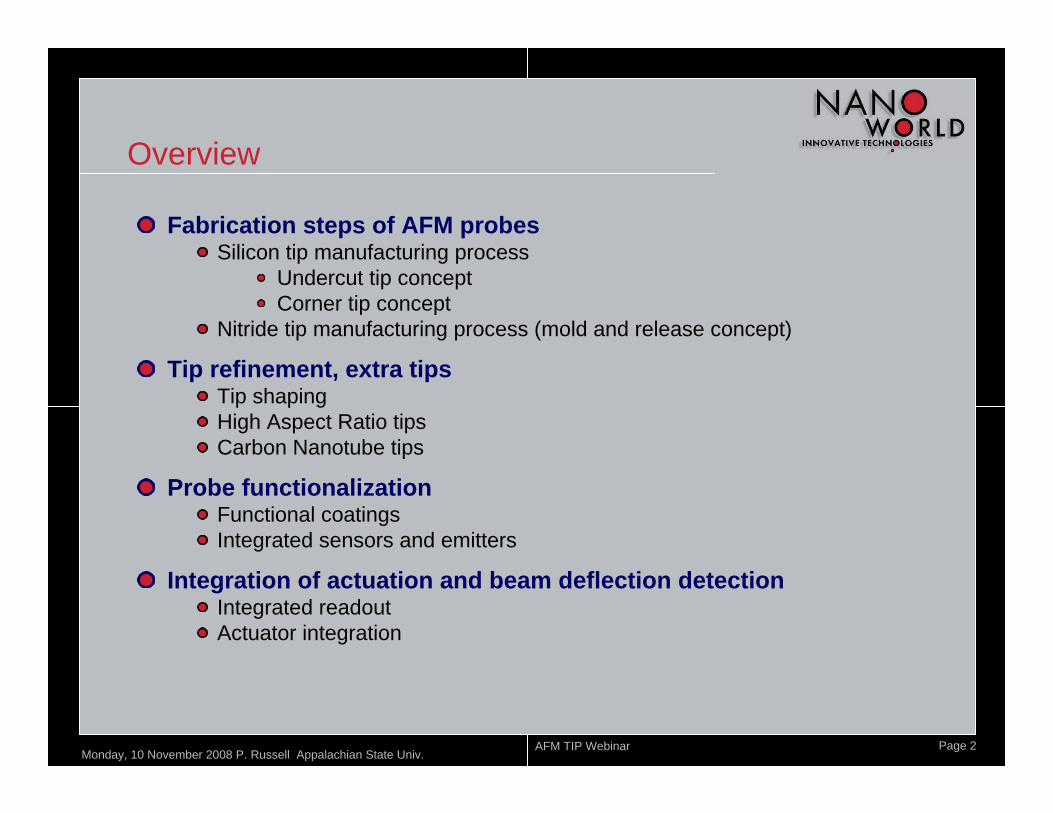
General remarks - Batch Fabrication
4-inch waferwith 388 probes
6-inch wafer with more than 1000 probes
Monday, 10 November 2008 P. Russell Appalachian State Univ. AFM TIP Webinar Page 4
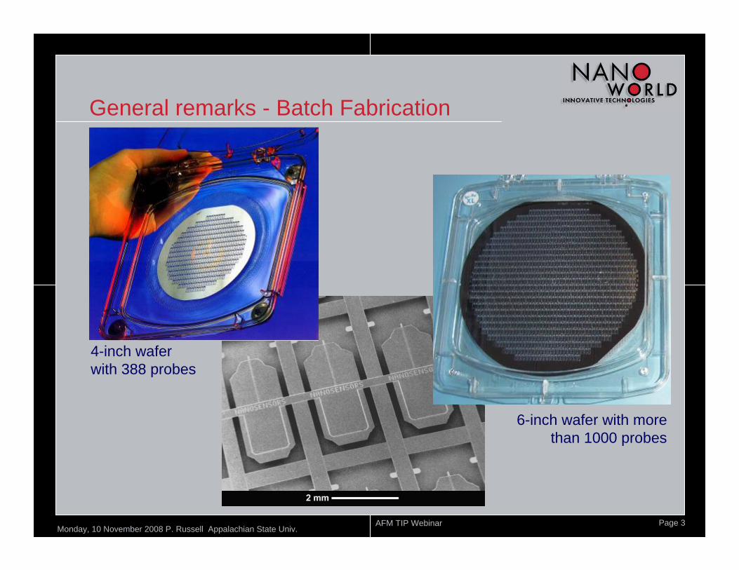
TipRadius < 15 nm
Tip height > 3 to 20µm
Cantilever BeamForce constant range: 0.01 to 50 N/m
Resonance frequency: 1 kHz to 1 MHzTypical Geometry
Length: 50 to 500 µmWidth: 20 to 50 µm
Thickness: 0.4 to 8 µm
HolderMacroscopic dimensions: 1.6 x 3.4 mm2
for easy handling and mounting into the SPM
Material: Single Crystalline Silicon or Silicon Nitride Thin Film
General remarks - AFM probe basics
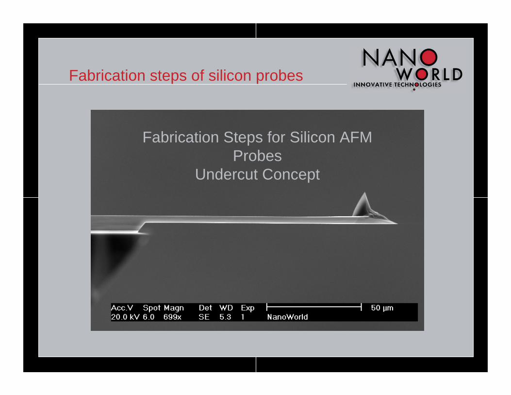
Fabrication Steps for Silicon AFM Probes
Undercut Concept
Fabrication steps of silicon probes
Monday, 10 November 2008 P. Russell Appalachian State Univ. AFM TIP Webinar Page 6
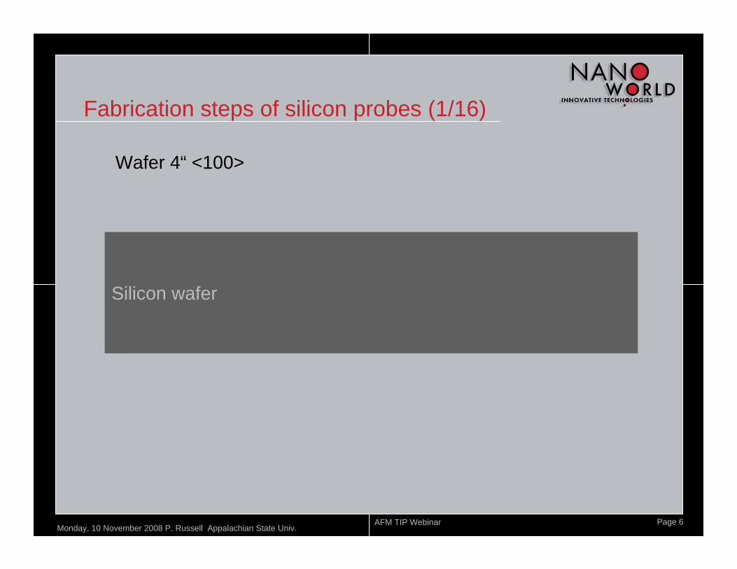
Silicon wafer
Wafer 4“ <100>
Fabrication steps of silicon probes (1/16)
Monday, 10 November 2008 P. Russell Appalachian State Univ. AFM TIP Webinar Page 7
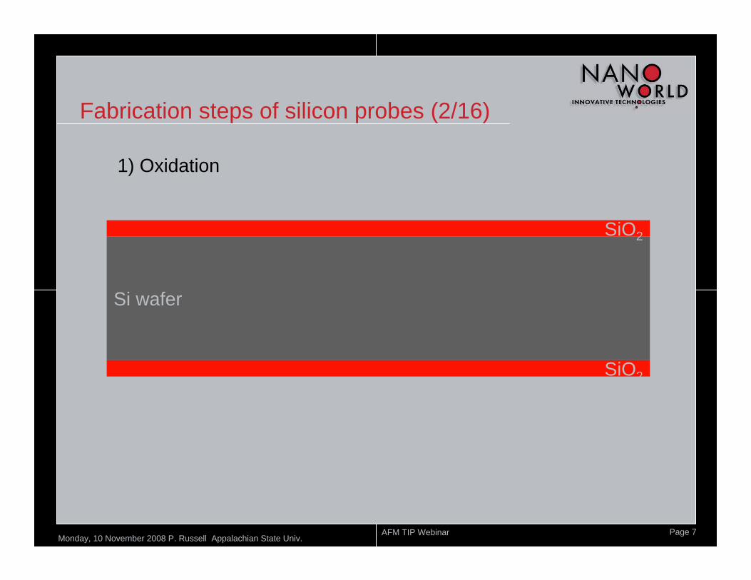
Si wafer
SiO2
SiO2
1) Oxidation
Fabrication steps of silicon probes (2/16)
Monday, 10 November 2008 P. Russell Appalachian State Univ. AFM TIP Webinar Page 8
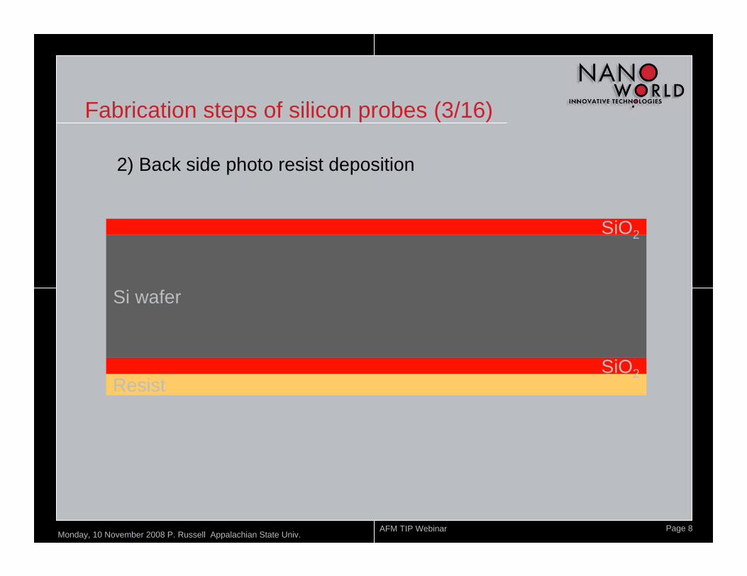
Si wafer
SiO2
ResistSiO2
2) Back side photo resist deposition
Fabrication steps of silicon probes (3/16)
Monday, 10 November 2008 P. Russell Appalachian State Univ. AFM TIP Webinar Page 9
Si wafer
SiO2
ResistSiO2
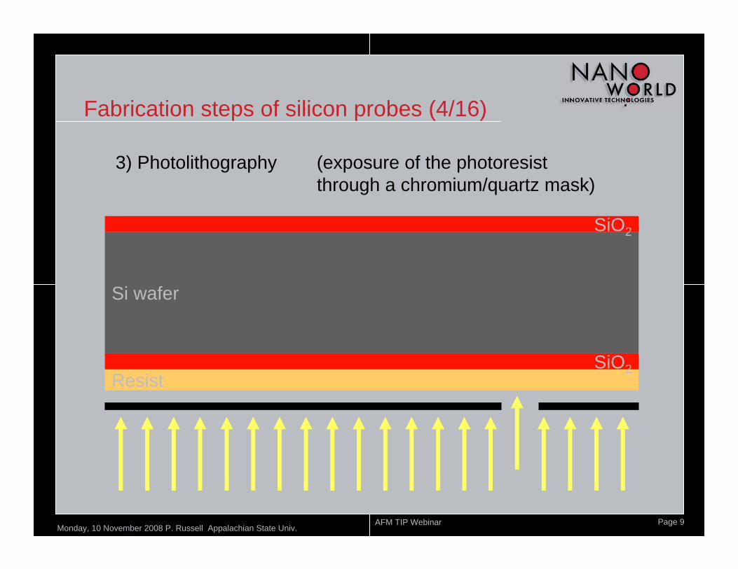
3) Photolithography (exposure of the photoresistthrough a chromium/quartz mask)
Fabrication steps of silicon probes (4/16)
Monday, 10 November 2008 P. Russell Appalachian State Univ. AFM TIP Webinar Page 10
Si wafer
SiO2
ResistSiO2
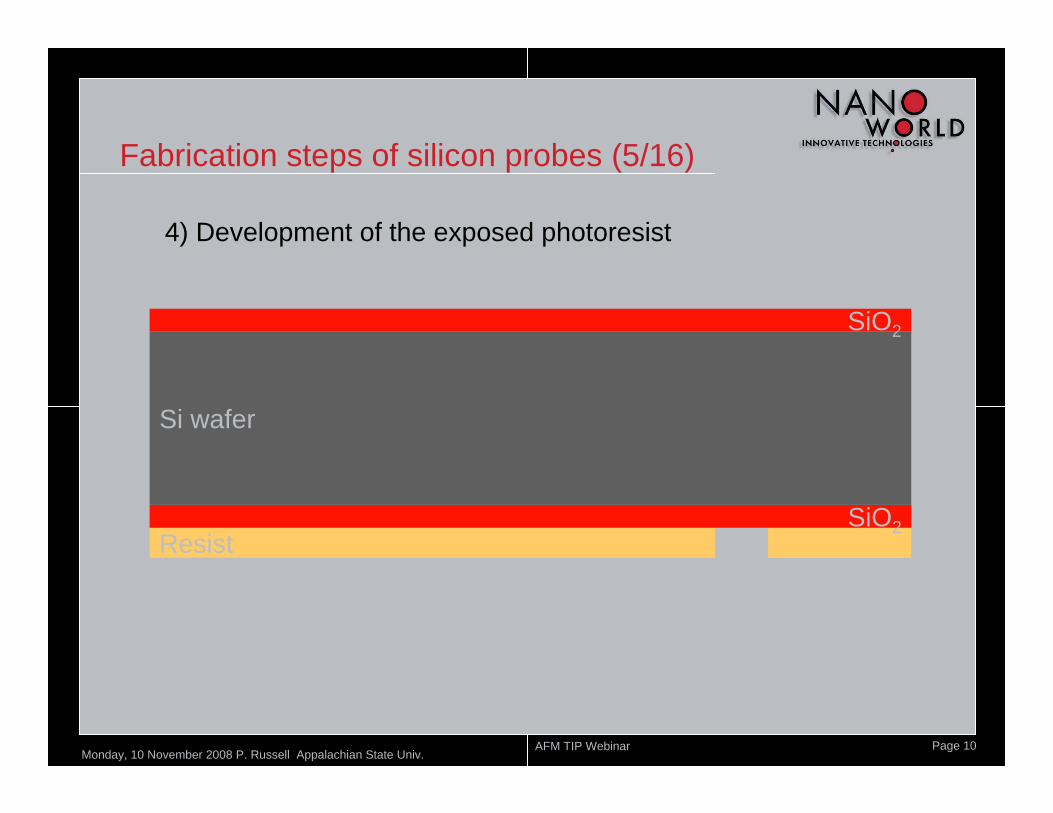
4) Development of the exposed photoresist
Fabrication steps of silicon probes (5/16)
Monday, 10 November 2008 P. Russell Appalachian State Univ. AFM TIP Webinar Page 11
Si wafer
SiO2
Resist
ResistSiO2
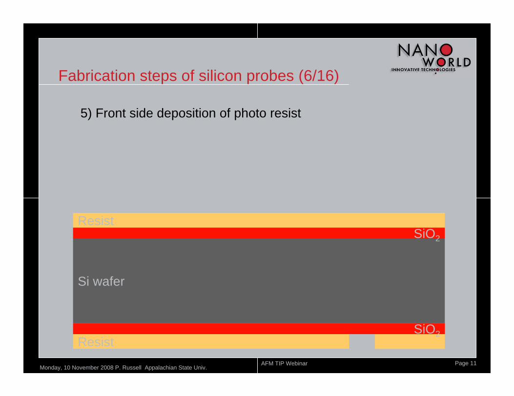
5) Front side deposition of photo resist
Fabrication steps of silicon probes (6/16)
Monday, 10 November 2008 P. Russell Appalachian State Univ. AFM TIP Webinar Page 12
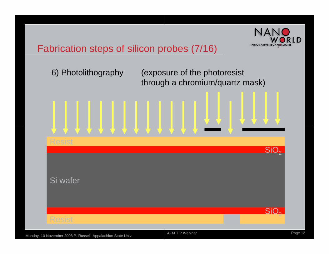
Fabrication steps of silicon probes (7/16)
Si wafer
SiO2
Resist
ResistSiO2
6) Photolithography (exposure of the photoresistthrough a chromium/quartz mask)
Monday, 10 November 2008 P. Russell Appalachian State Univ. AFM TIP Webinar Page 13
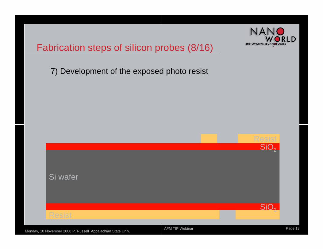
Fabrication steps of silicon probes (8/16)
Si wafer
SiO2
ResistSiO2
7) Development of the exposed photo resist
Resist
Monday, 10 November 2008 P. Russell Appalachian State Univ. AFM TIP Webinar Page 14
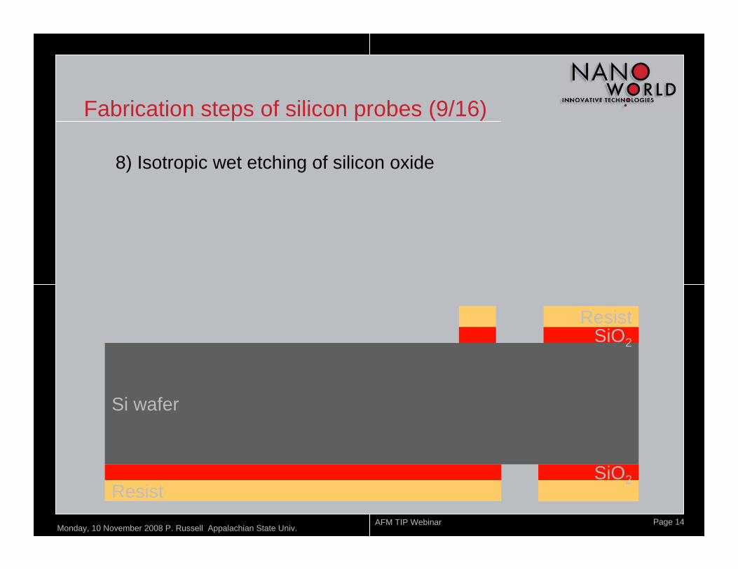
Si wafer
ResistSiO2
SiO2
8) Isotropic wet etching of silicon oxide
Resist
Fabrication steps of silicon probes (9/16)
Monday, 10 November 2008 P. Russell Appalachian State Univ. AFM TIP Webinar Page 15
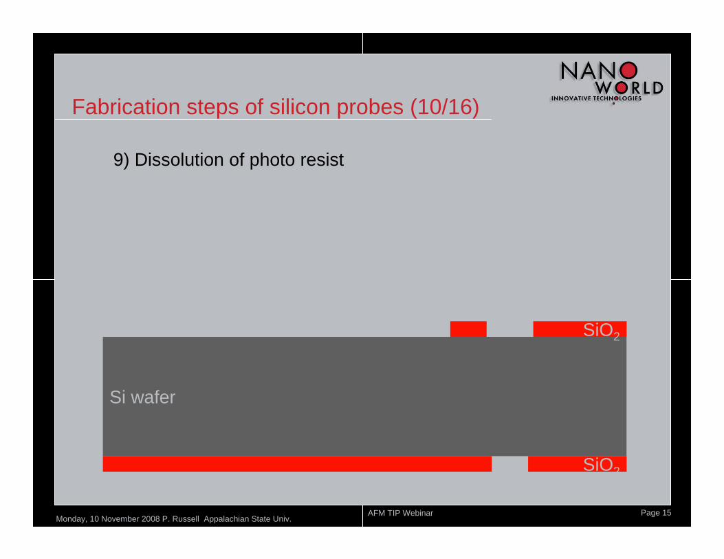
Si wafer
SiO2
SiO2
9) Dissolution of photo resist
Fabrication steps of silicon probes (10/16)

Monday, 10 November 2008 P. Russell Appalachian State Univ. AFM TIP Webinar Page 16
SiO2
Si wafer
SiO2
10) Anisotropic wet etching of silicon by KOHdone in several steps
Fabrication steps of silicon probes (11/16)
Monday, 10 November 2008 P. Russell Appalachian State Univ. AFM TIP Webinar Page 17
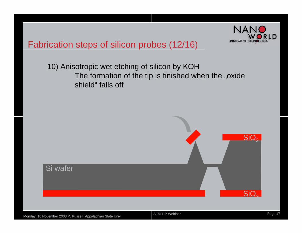
SiO2
Si wafer
SiO2
10) Anisotropic wet etching of silicon by KOHThe formation of the tip is finished when the „oxide shield“ falls off
Fabrication steps of silicon probes (12/16)
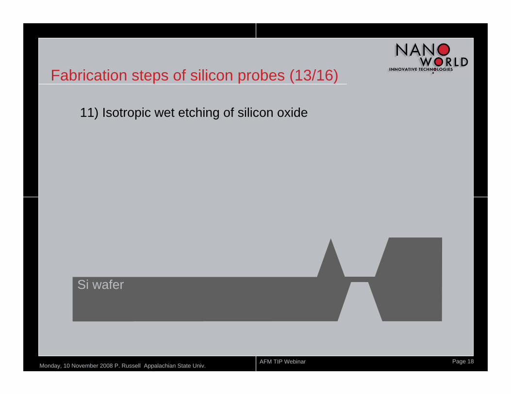
Monday, 10 November 2008 P. Russell Appalachian State Univ. AFM TIP Webinar Page 18
Si wafer
11) Isotropic wet etching of silicon oxide
Fabrication steps of silicon probes (13/16)
Monday, 10 November 2008 P. Russell Appalachian State Univ. AFM TIP Webinar Page 19
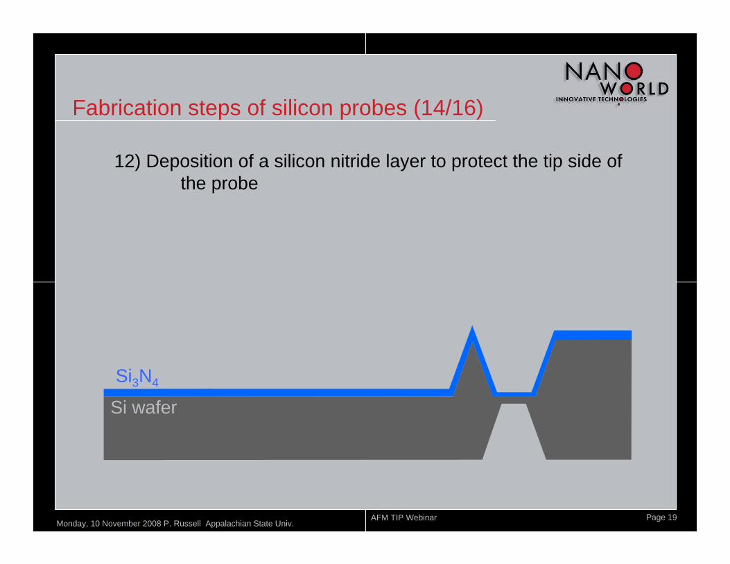
Fabrication steps of silicon probes (14/16)
Si wafer
Si3N4
12) Deposition of a silicon nitride layer to protect the tip side of the probe
Monday, 10 November 2008 P. Russell Appalachian State Univ. AFM TIP Webinar Page 20
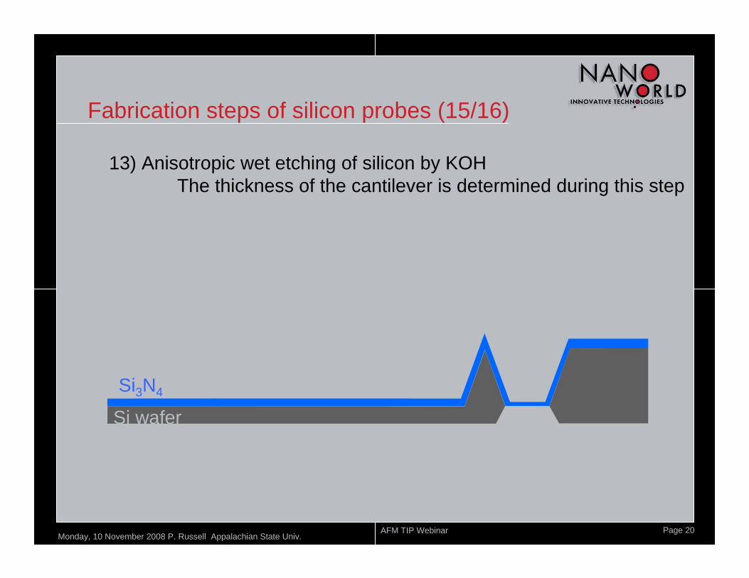
Si Wafer
13) Anisotropic wet etching of silicon by KOHThe thickness of the cantilever is determined during this step
Si3N4
Si wafer
Fabrication steps of silicon probes (15/16)
Monday, 10 November 2008 P. Russell Appalachian State Univ. AFM TIP Webinar Page 21
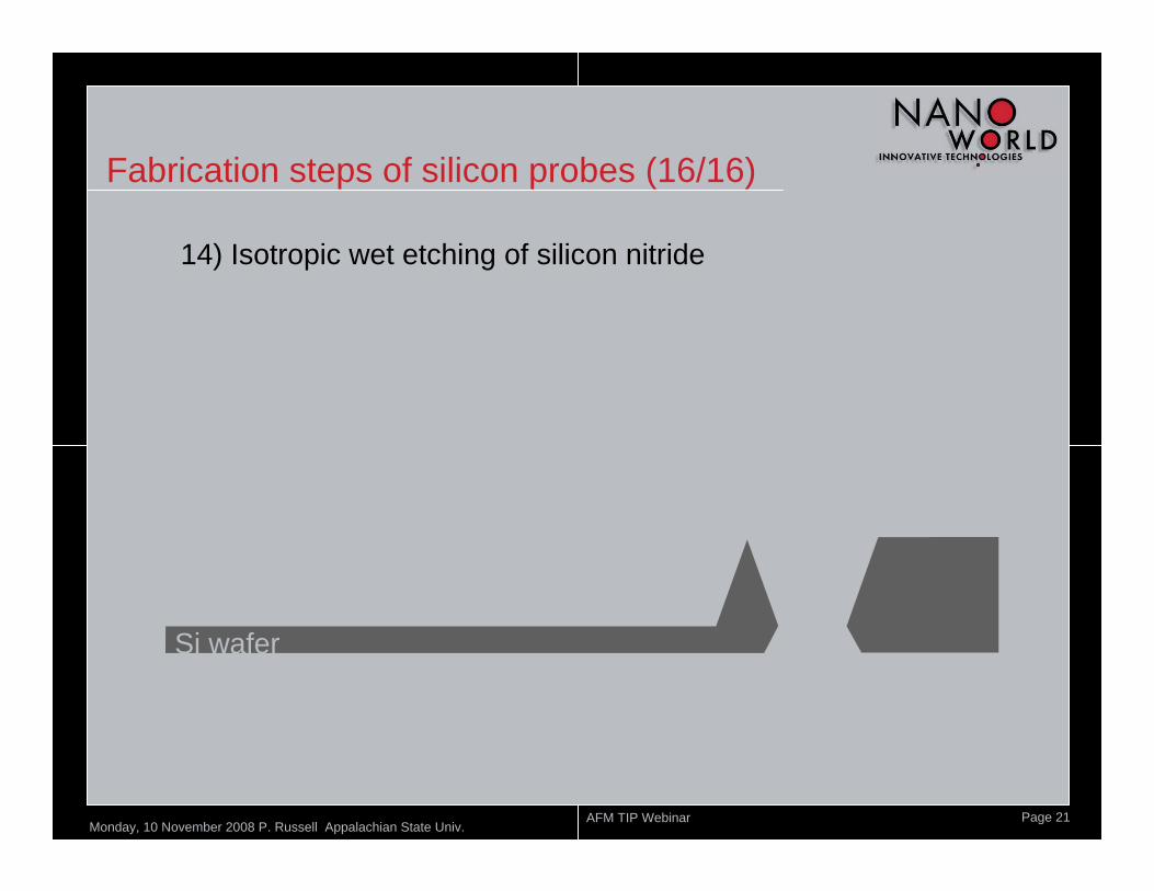
Si Wafer
14) Isotropic wet etching of silicon nitride
Si wafer
Fabrication steps of silicon probes (16/16)
Monday, 10 November 2008 P. Russell Appalachian State Univ. AFM TIP Webinar Page 22
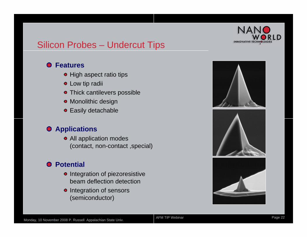
Silicon Probes – Undercut Tips
FeaturesHigh aspect ratio tipsLow tip radiiThick cantilevers possibleMonolithic designEasily detachable
ApplicationsAll application modes (contact, non-contact ,special)
PotentialIntegration of piezoresistive beam deflection detectionIntegration of sensors (semiconductor)
Monday, 10 November 2008 P. Russell Appalachian State Univ. AFM TIP Webinar Page 23
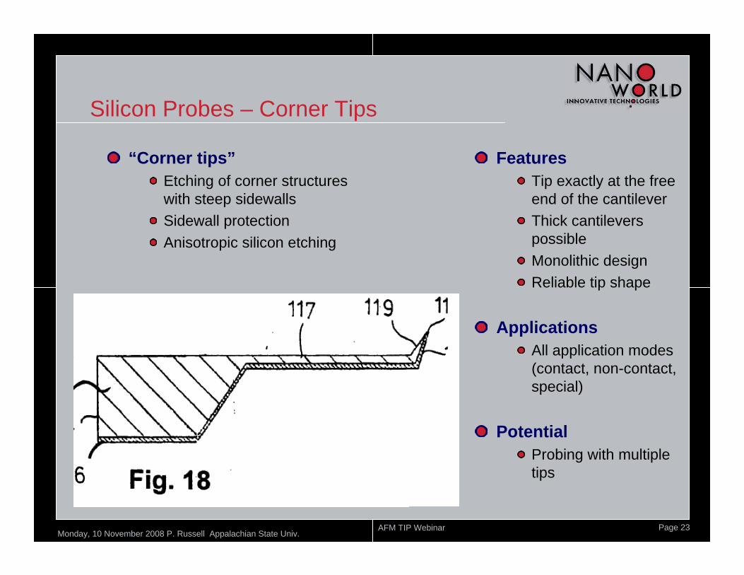
Silicon Probes – Corner Tips
“Corner tips”Etching of corner structures with steep sidewallsSidewall protectionAnisotropic silicon etching
FeaturesTip exactly at the free end of the cantileverThick cantilevers possibleMonolithic designReliable tip shape
ApplicationsAll application modes (contact, non-contact, special)
PotentialProbing with multiple tips
Monday, 10 November 2008 P. Russell Appalachian State Univ. AFM TIP Webinar Page 24
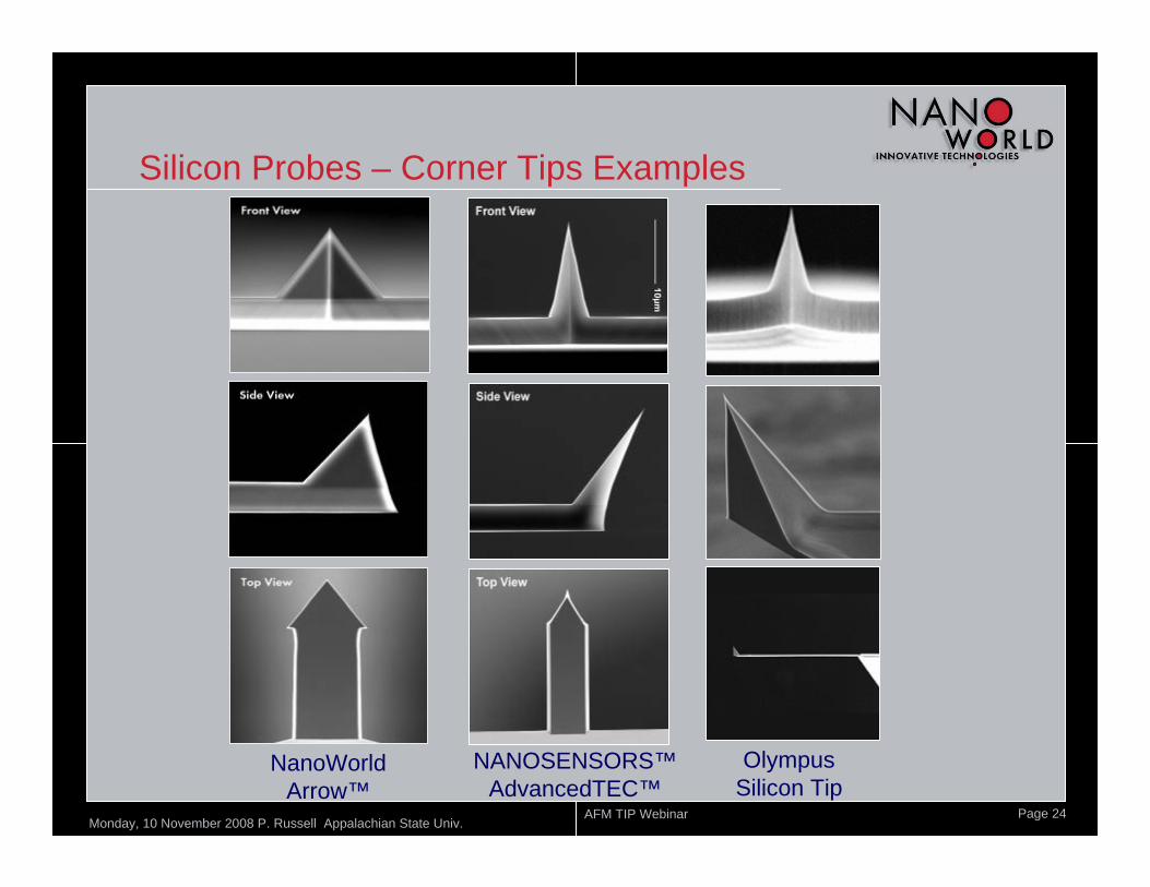
Silicon Probes – Corner Tips Examples
NanoWorldArrow™
NANOSENSORS™AdvancedTEC™
Olympus Silicon Tip
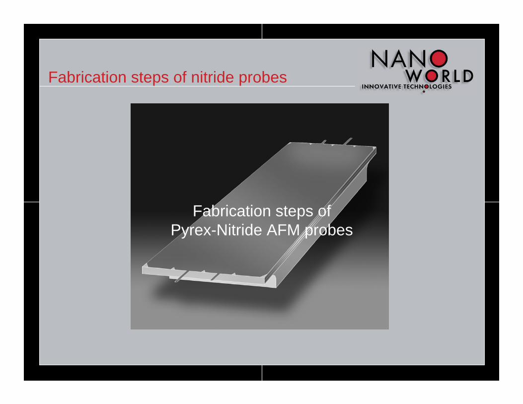
Fabrication steps of Pyrex-Nitride AFM probes
Fabrication steps of nitride probes
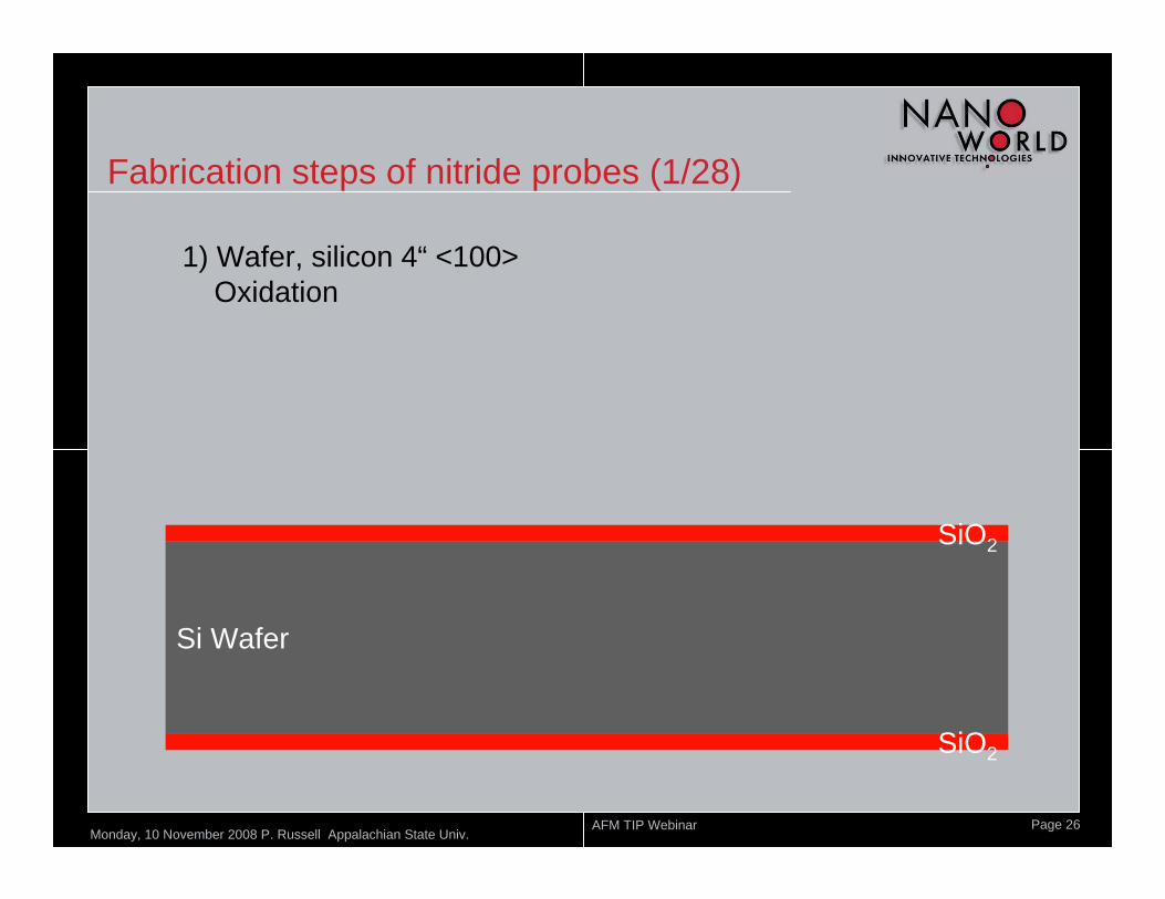
Monday, 10 November 2008 P. Russell Appalachian State Univ. AFM TIP Webinar Page 26
Si Wafer
SiO2
SiO2
1) Wafer, silicon 4“ <100>Oxidation
Fabrication steps of nitride probes (1/28)
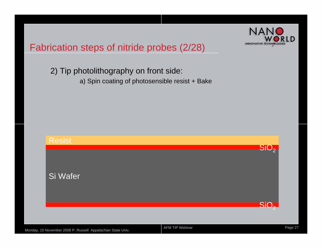
Monday, 10 November 2008 P. Russell Appalachian State Univ. AFM TIP Webinar Page 27
Si Wafer
SiO2
Resist
SiO2
2) Tip photolithography on front side:a) Spin coating of photosensible resist + Bake
Fabrication steps of nitride probes (2/28)
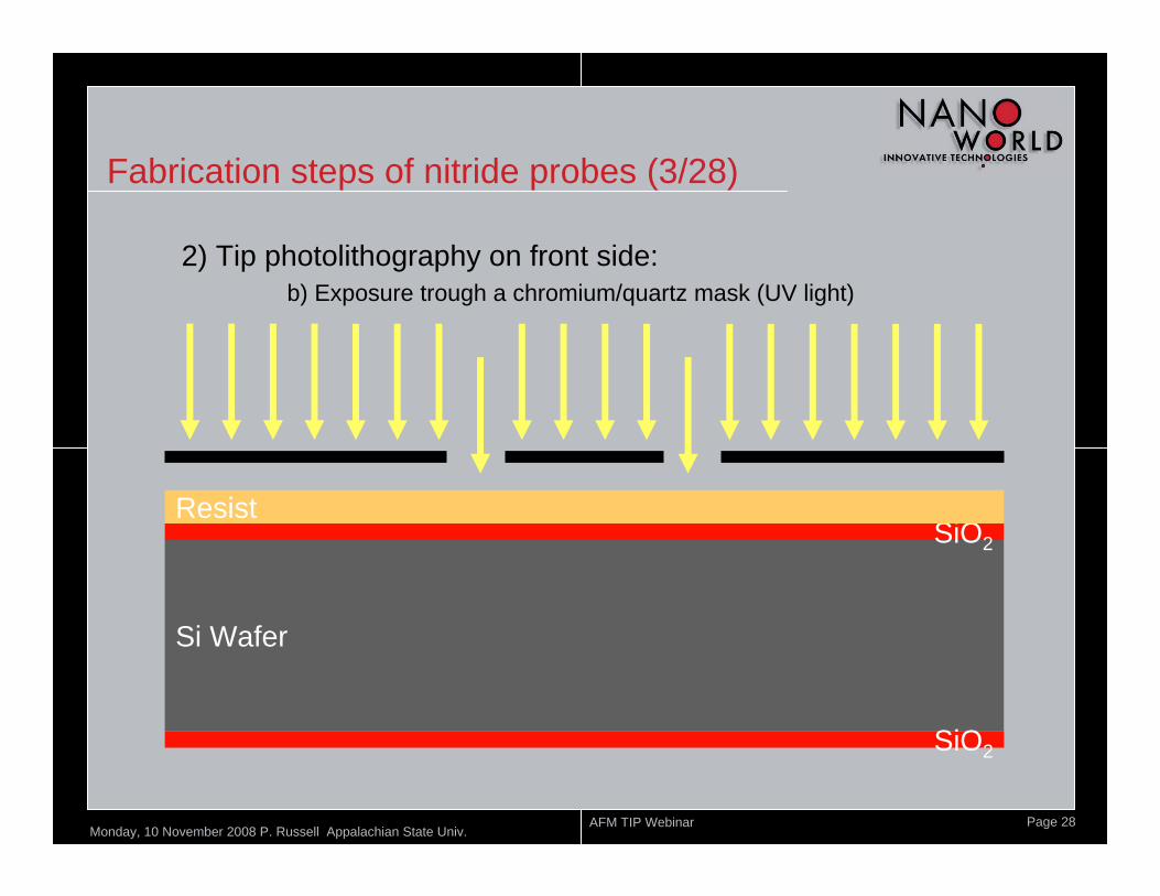
Monday, 10 November 2008 P. Russell Appalachian State Univ. AFM TIP Webinar Page 28
Si Wafer
SiO2
Resist
SiO2
2) Tip photolithography on front side:b) Exposure trough a chromium/quartz mask (UV light)
Fabrication steps of nitride probes (3/28)
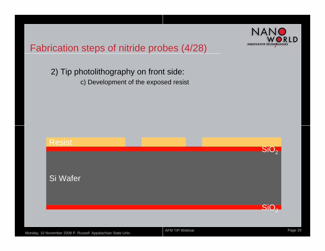
Monday, 10 November 2008 P. Russell Appalachian State Univ. AFM TIP Webinar Page 29
Si Wafer
SiO2
Resist
SiO2
2) Tip photolithography on front side:c) Development of the exposed resist
Fabrication steps of nitride probes (4/28)
Monday, 10 November 2008 P. Russell Appalachian State Univ. AFM TIP Webinar Page 30
Si Wafer
SiO2
Resist
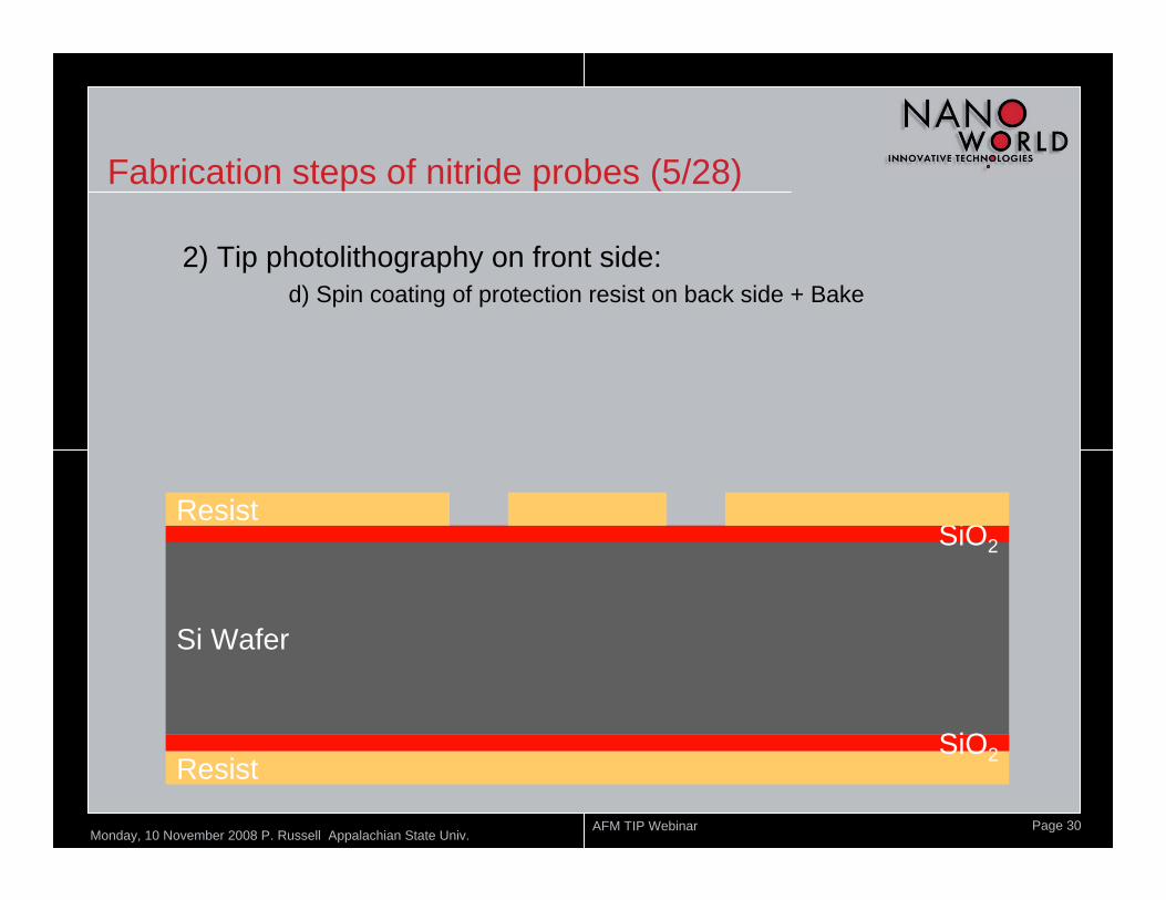
2) Tip photolithography on front side:d) Spin coating of protection resist on back side + Bake
ResistSiO2
Fabrication steps of nitride probes (5/28)
Monday, 10 November 2008 P. Russell Appalachian State Univ. AFM TIP Webinar Page 31
Si Wafer
SiO2
Resist
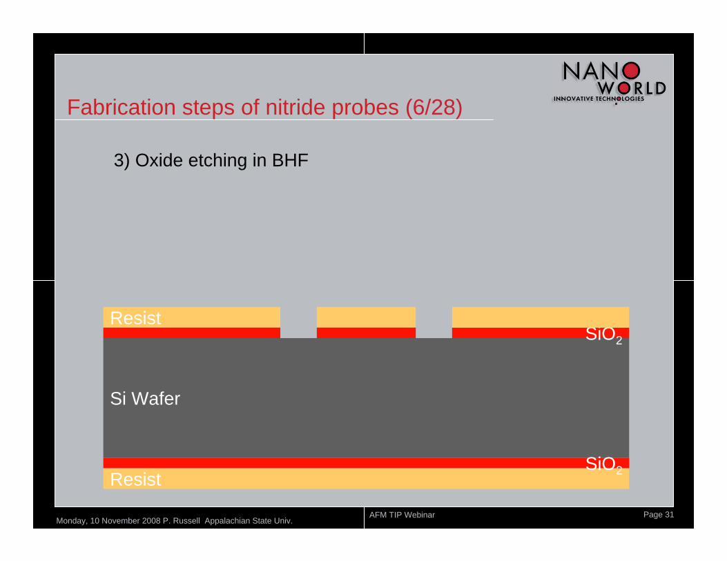
3) Oxide etching in BHF
ResistSiO2
Fabrication steps of nitride probes (6/28)
Monday, 10 November 2008 P. Russell Appalachian State Univ. AFM TIP Webinar Page 32
Si Wafer
SiO2
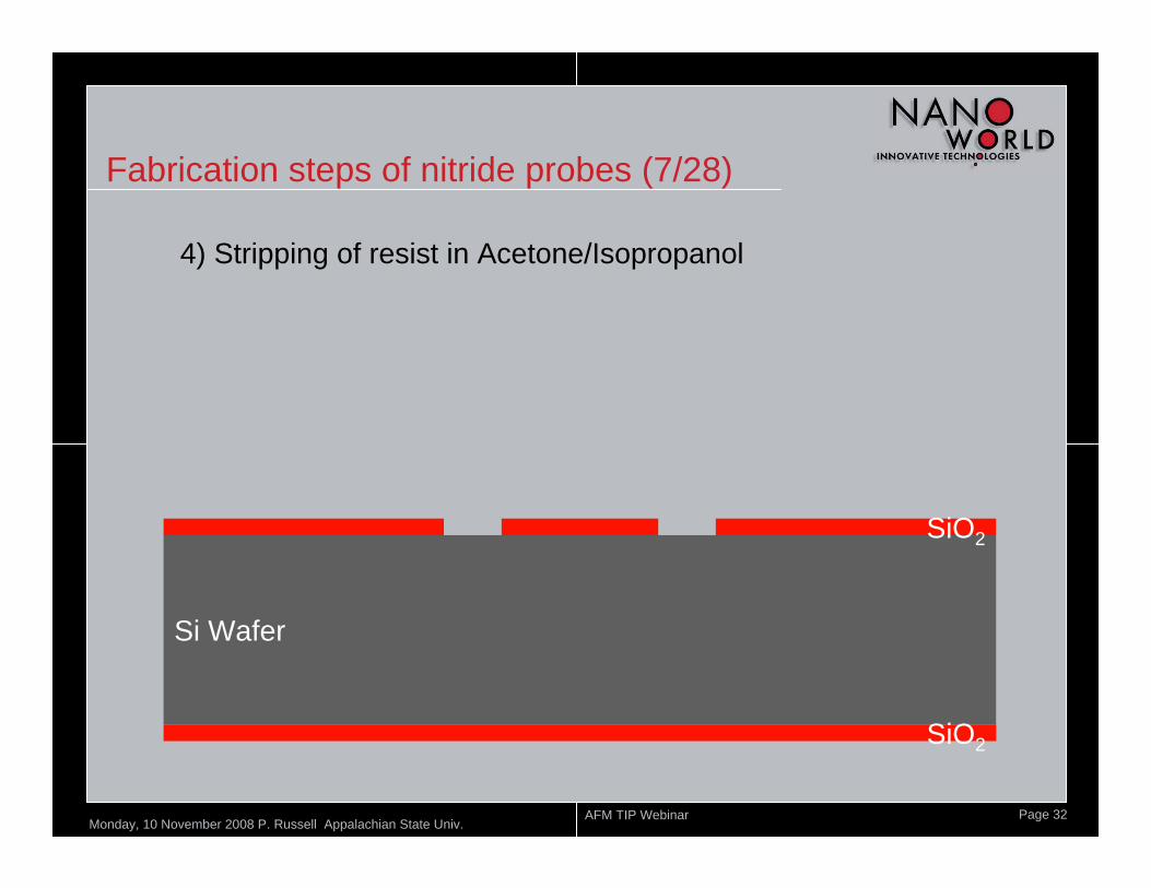
4) Stripping of resist in Acetone/Isopropanol
SiO2
Fabrication steps of nitride probes (7/28)
Monday, 10 November 2008 P. Russell Appalachian State Univ. AFM TIP Webinar Page 33
Si Wafer
SiO2
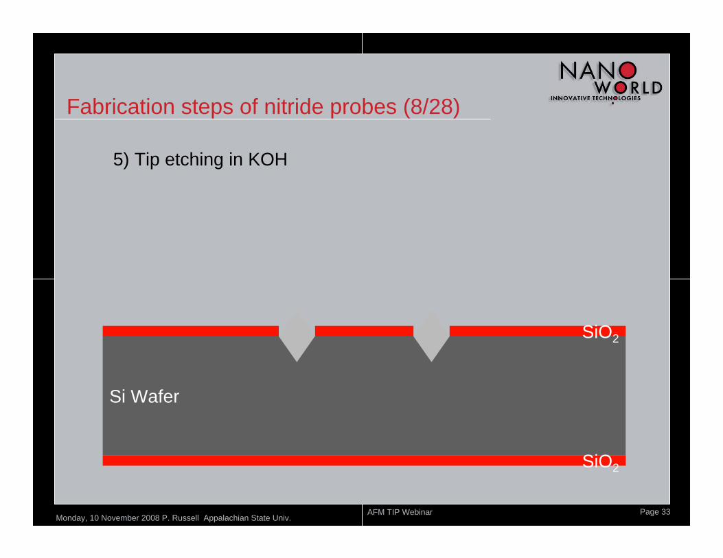
5) Tip etching in KOH
SiO2
Fabrication steps of nitride probes (8/28)
Monday, 10 November 2008 P. Russell Appalachian State Univ. AFM TIP Webinar Page 34
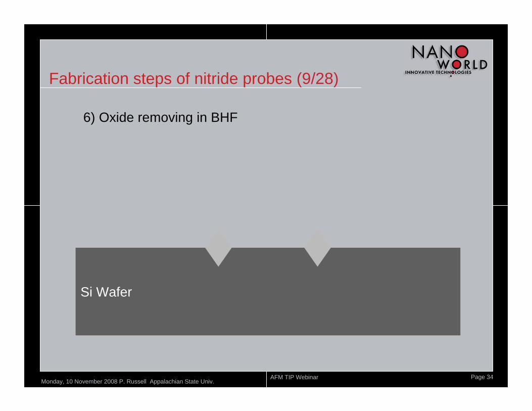
Si Wafer
6) Oxide removing in BHF
Fabrication steps of nitride probes (9/28)
Monday, 10 November 2008 P. Russell Appalachian State Univ. AFM TIP Webinar Page 35
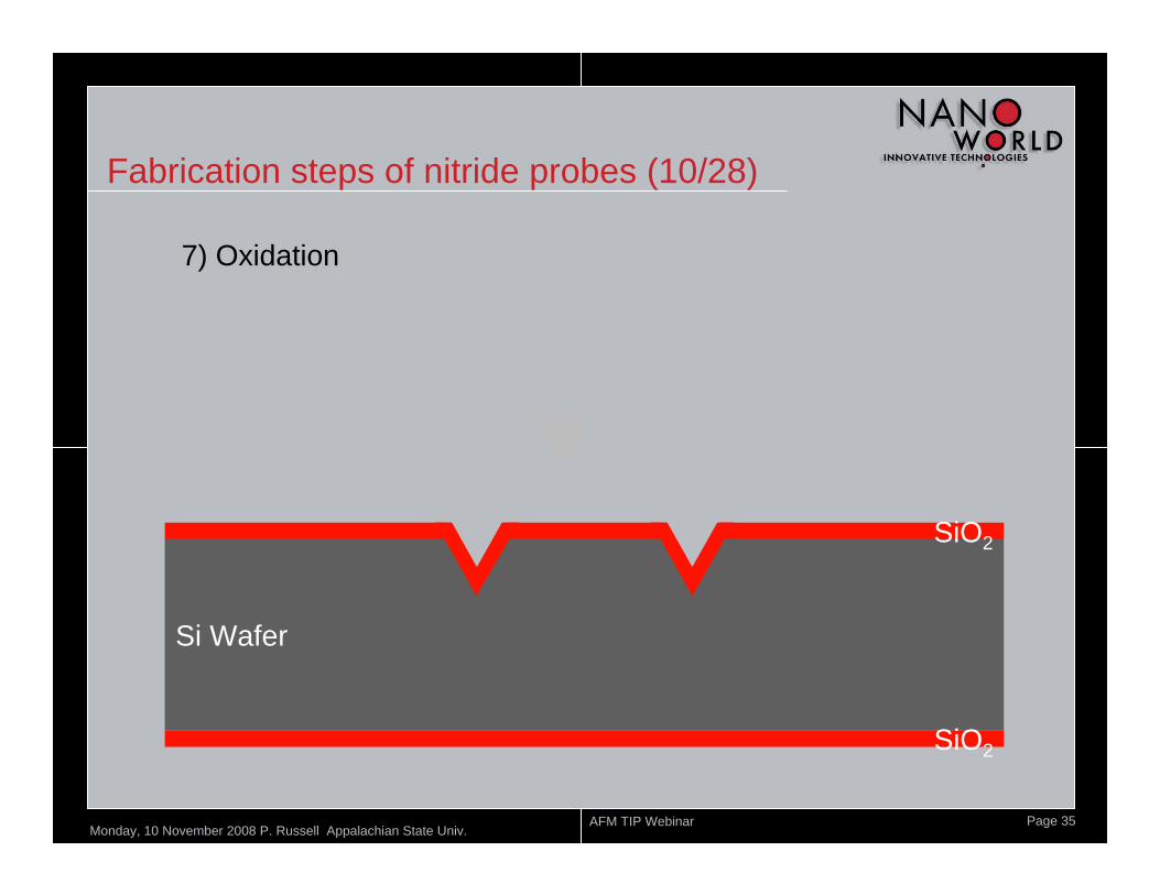
Si Wafer
SiO2
7) Oxidation
SiO2
Fabrication steps of nitride probes (10/28)
Monday, 10 November 2008 P. Russell Appalachian State Univ. AFM TIP Webinar Page 36
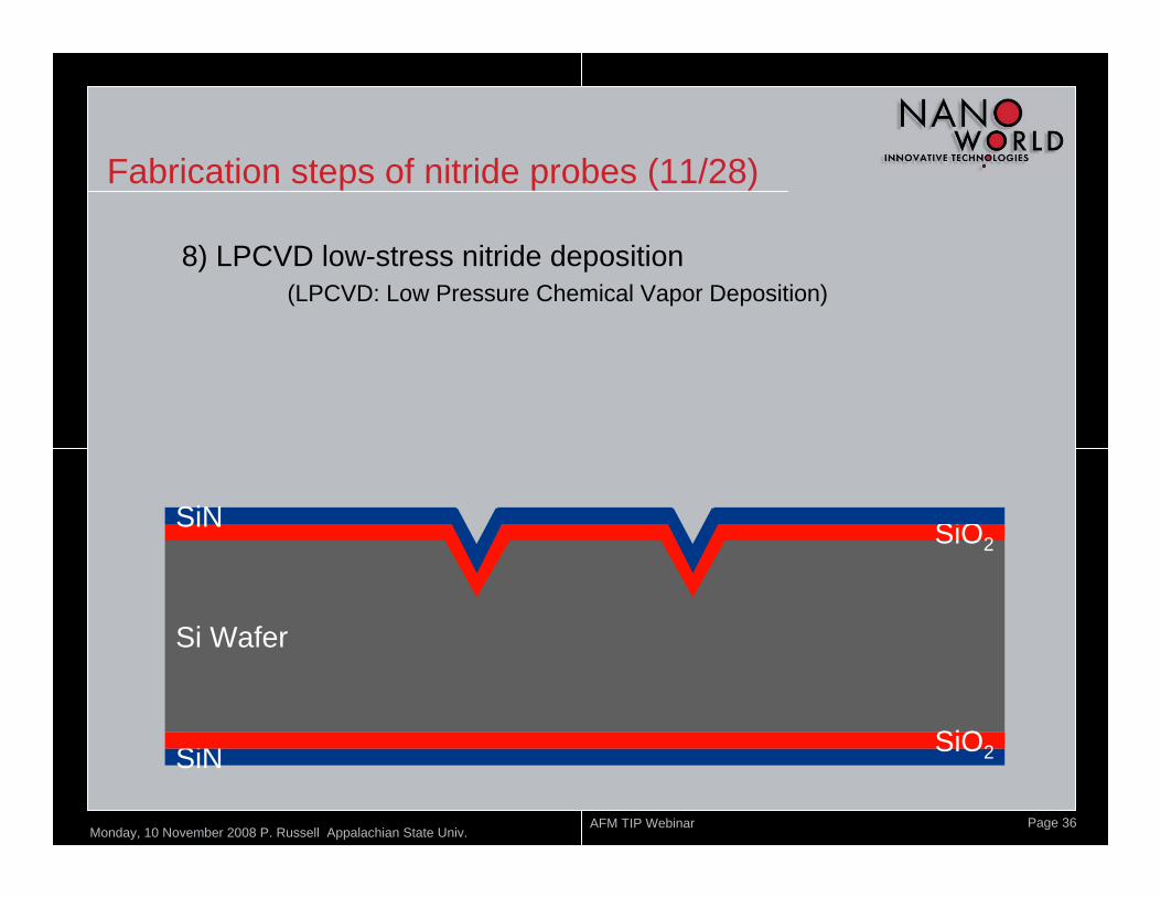
Si Wafer
SiO2
8) LPCVD low-stress nitride deposition(LPCVD: Low Pressure Chemical Vapor Deposition)
SiN
SiN SiO2
Fabrication steps of nitride probes (11/28)
Monday, 10 November 2008 P. Russell Appalachian State Univ. AFM TIP Webinar Page 37
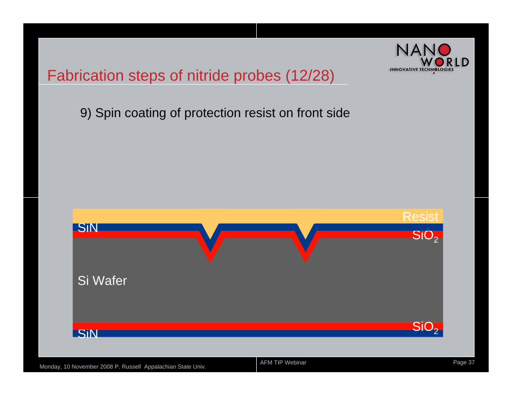
Si Wafer
SiO2
9) Spin coating of protection resist on front side
SiN
SiN SiO2
Resist
Fabrication steps of nitride probes (12/28)
Monday, 10 November 2008 P. Russell Appalachian State Univ. AFM TIP Webinar Page 38
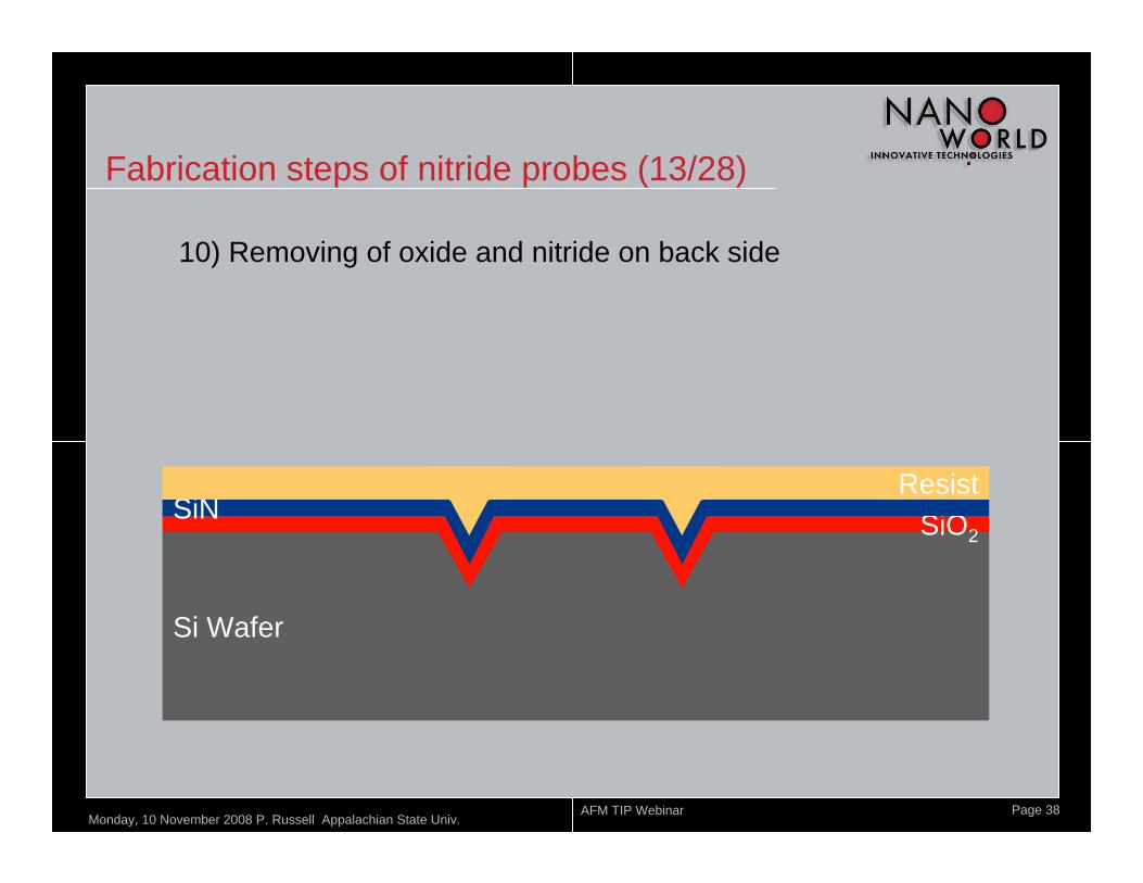
Si Wafer
SiO2
10) Removing of oxide and nitride on back side
SiNResist
Fabrication steps of nitride probes (13/28)
Monday, 10 November 2008 P. Russell Appalachian State Univ. AFM TIP Webinar Page 39
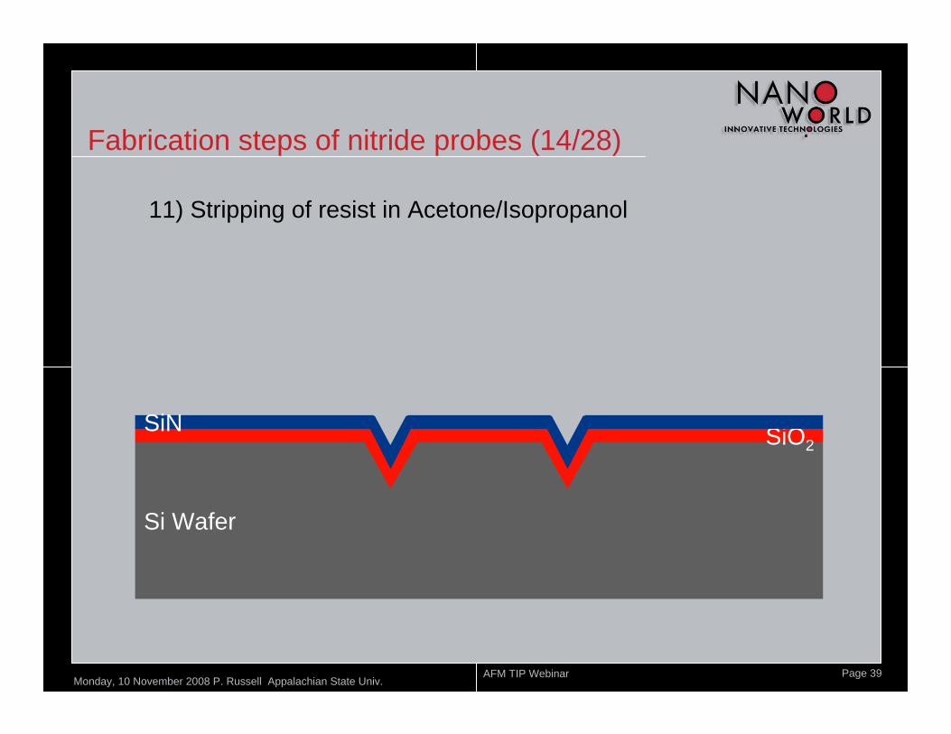
Si Wafer
SiO2
11) Stripping of resist in Acetone/Isopropanol
SiN
Fabrication steps of nitride probes (14/28)
Monday, 10 November 2008 P. Russell Appalachian State Univ. AFM TIP Webinar Page 40
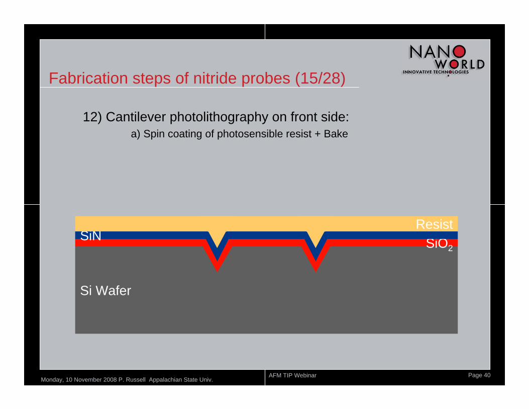
Si Wafer
SiO2SiN
Resist
12) Cantilever photolithography on front side:a) Spin coating of photosensible resist + Bake
Fabrication steps of nitride probes (15/28)
Monday, 10 November 2008 P. Russell Appalachian State Univ. AFM TIP Webinar Page 41
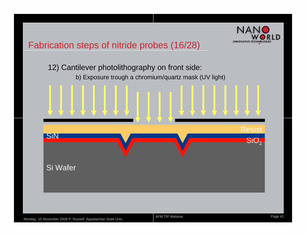
Si Wafer
SiO2SiN
Resist
12) Cantilever photolithography on front side:b) Exposure trough a chromium/quartz mask (UV light)
Fabrication steps of nitride probes (16/28)
Monday, 10 November 2008 P. Russell Appalachian State Univ. AFM TIP Webinar Page 42
Si Wafer
SiO2SiN
Resist
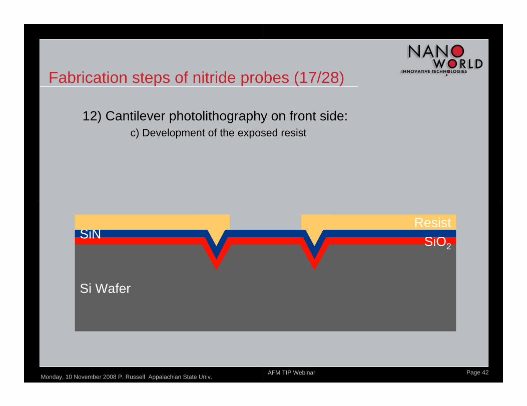
12) Cantilever photolithography on front side:c) Development of the exposed resist
Fabrication steps of nitride probes (17/28)
Monday, 10 November 2008 P. Russell Appalachian State Univ. AFM TIP Webinar Page 43
Si Wafer
SiO2SiN
Resist
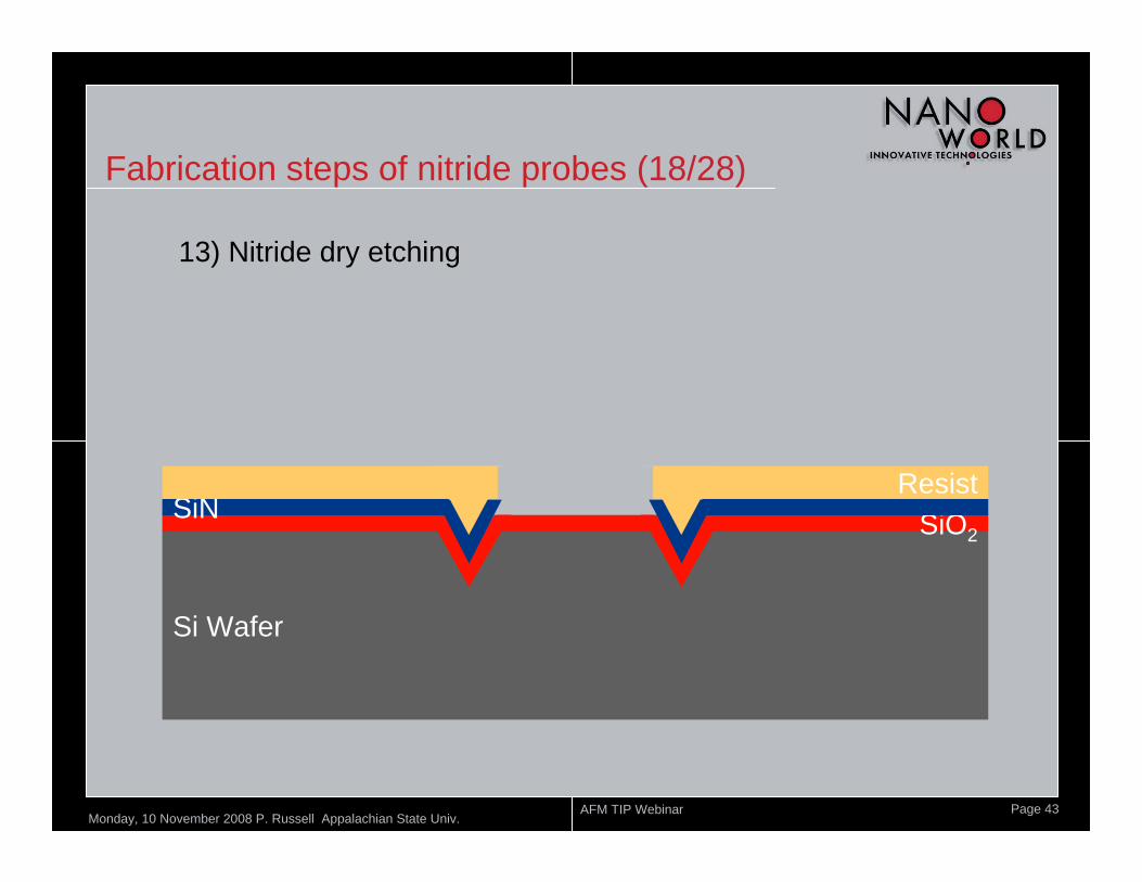
13) Nitride dry etching
Fabrication steps of nitride probes (18/28)
Monday, 10 November 2008 P. Russell Appalachian State Univ. AFM TIP Webinar Page 44
Si Wafer
SiO2
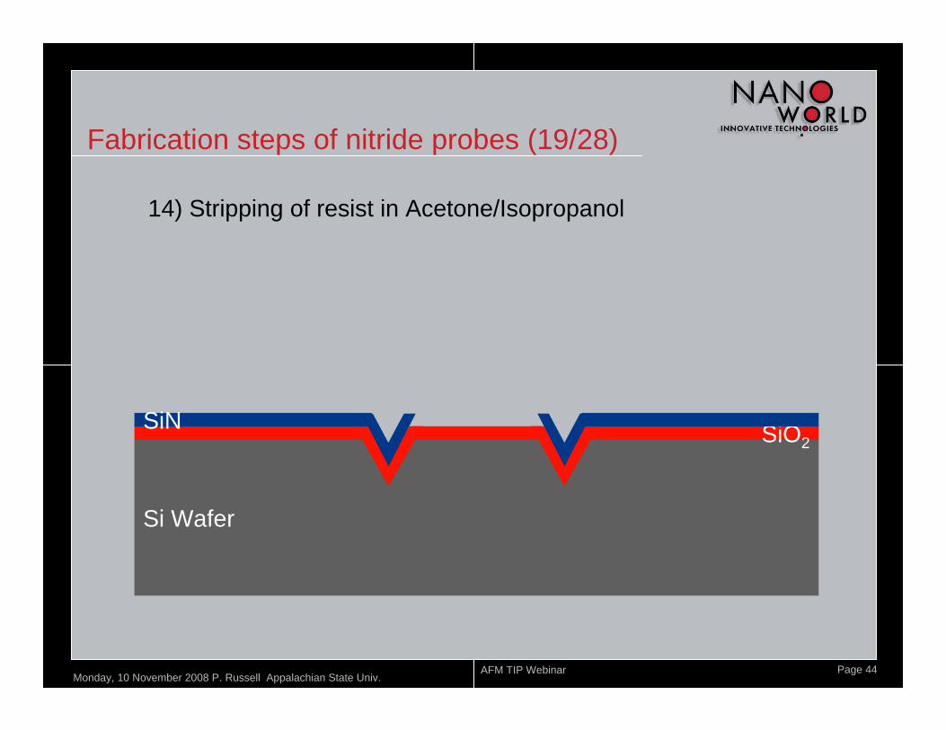
14) Stripping of resist in Acetone/Isopropanol
SiN
Fabrication steps of nitride probes (19/28)
Monday, 10 November 2008 P. Russell Appalachian State Univ. AFM TIP Webinar Page 45
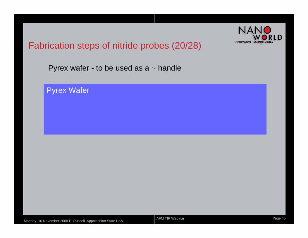
Pyrex wafer - to be used as a ~ handle
Pyrex Wafer
Fabrication steps of nitride probes (20/28)
Monday, 10 November 2008 P. Russell Appalachian State Univ. AFM TIP Webinar Page 46
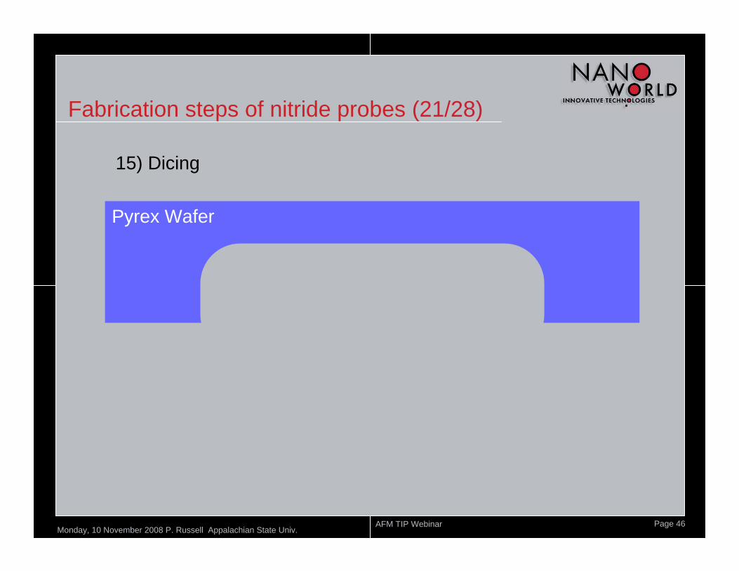
15) Dicing
Pyrex Wafer
Fabrication steps of nitride probes (21/28)
Monday, 10 November 2008 P. Russell Appalachian State Univ. AFM TIP Webinar Page 47
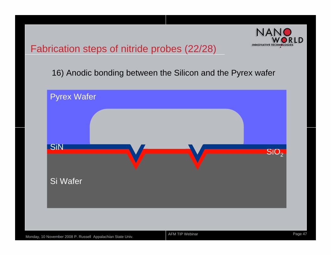
Pyrex Wafer
Si Wafer
SiO2
16) Anodic bonding between the Silicon and the Pyrex wafer
SiN
Fabrication steps of nitride probes (22/28)
Monday, 10 November 2008 P. Russell Appalachian State Univ. AFM TIP Webinar Page 48
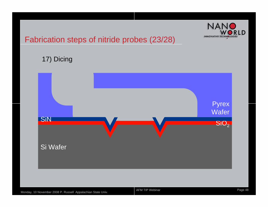
PyrexWafer
Si Wafer
SiO2SiN
17) Dicing
Fabrication steps of nitride probes (23/28)
Monday, 10 November 2008 P. Russell Appalachian State Univ. AFM TIP Webinar Page 49
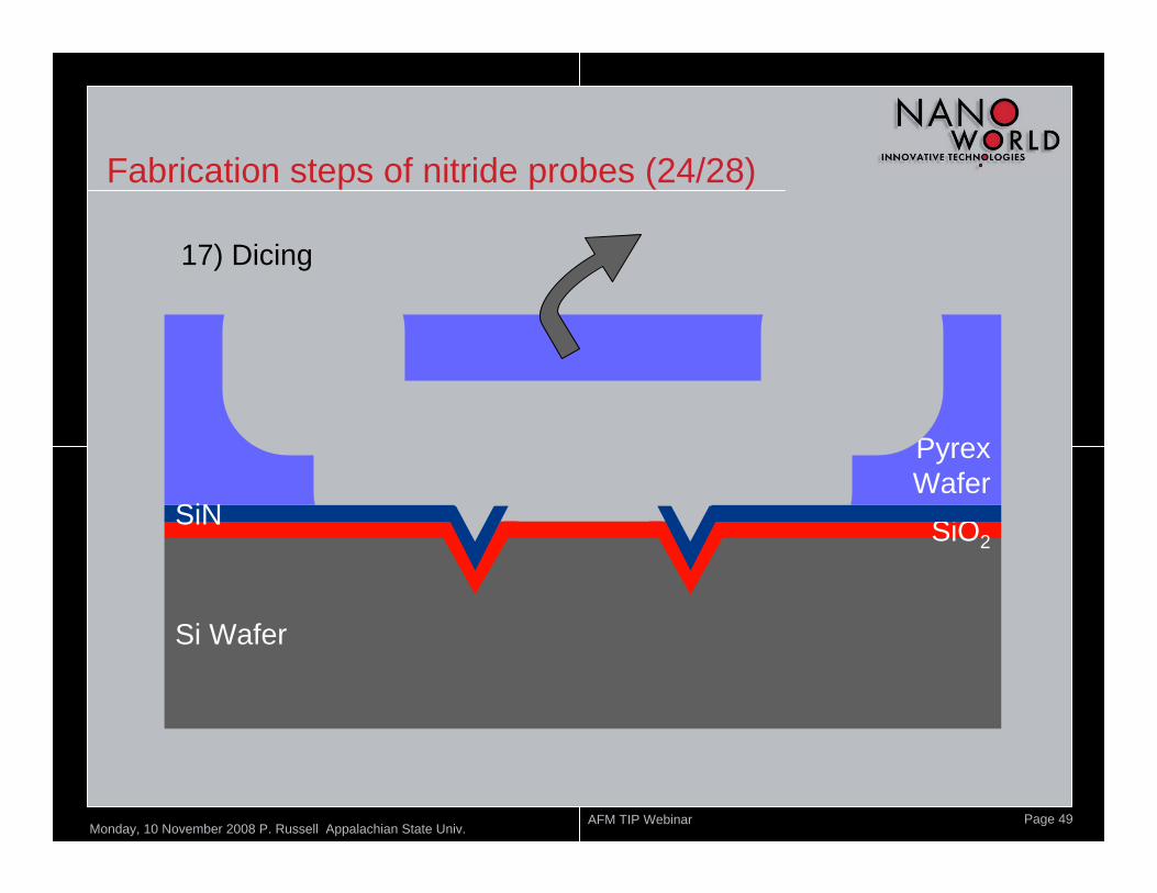
PyrexWafer
Si Wafer
SiO2SiN
17) Dicing
Fabrication steps of nitride probes (24/28)
Monday, 10 November 2008 P. Russell Appalachian State Univ. AFM TIP Webinar Page 50
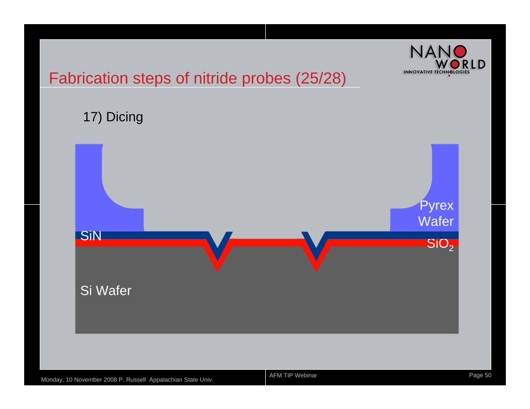
PyrexWafer
Si Wafer
SiO2SiN
17) Dicing
Fabrication steps of nitride probes (25/28)
Monday, 10 November 2008 P. Russell Appalachian State Univ. AFM TIP Webinar Page 51
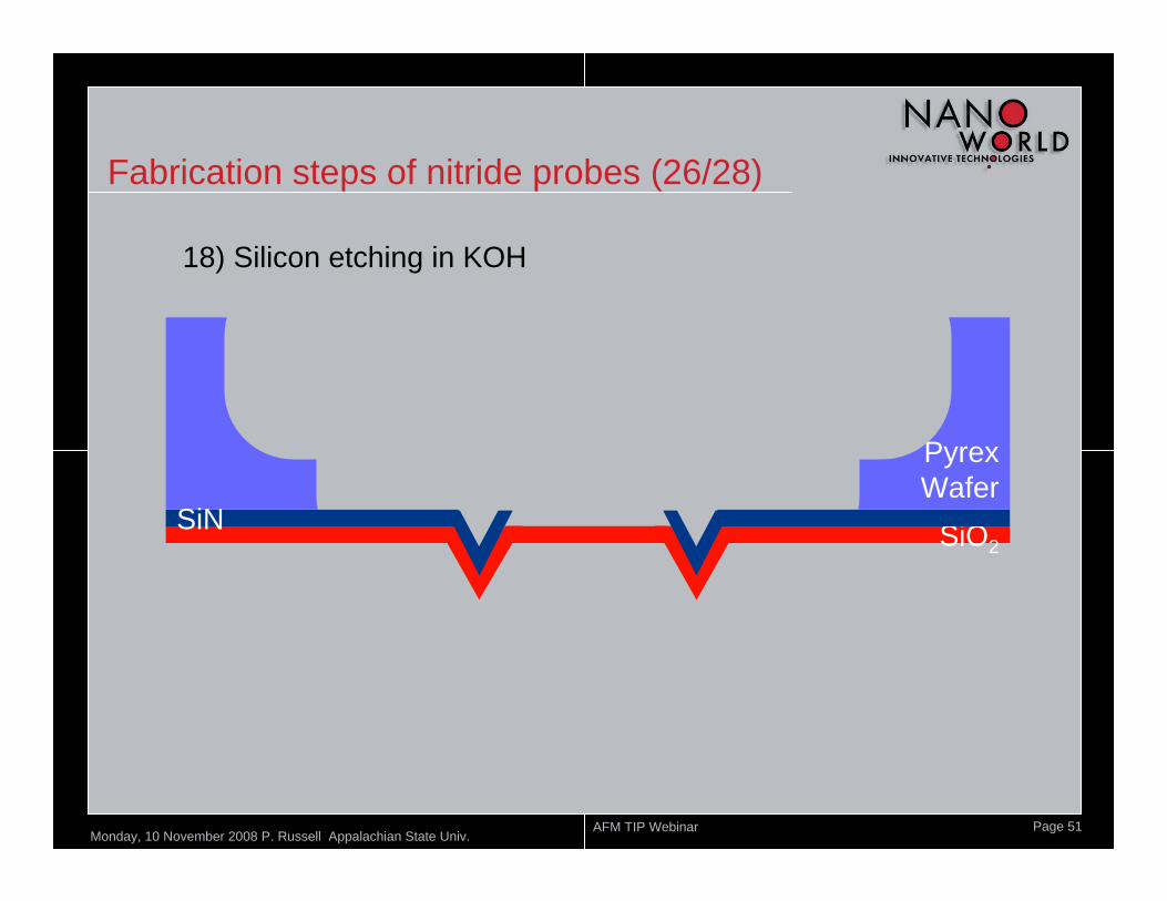
PyrexWafer
SiO2SiN
18) Silicon etching in KOH
Fabrication steps of nitride probes (26/28)
Monday, 10 November 2008 P. Russell Appalachian State Univ. AFM TIP Webinar Page 52
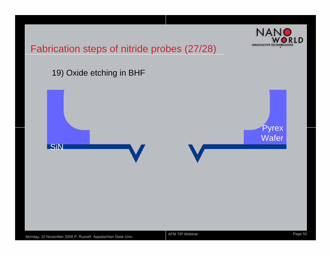
PyrexWafer
SiN
19) Oxide etching in BHF
Fabrication steps of nitride probes (27/28)
Monday, 10 November 2008 P. Russell Appalachian State Univ. AFM TIP Webinar Page 53
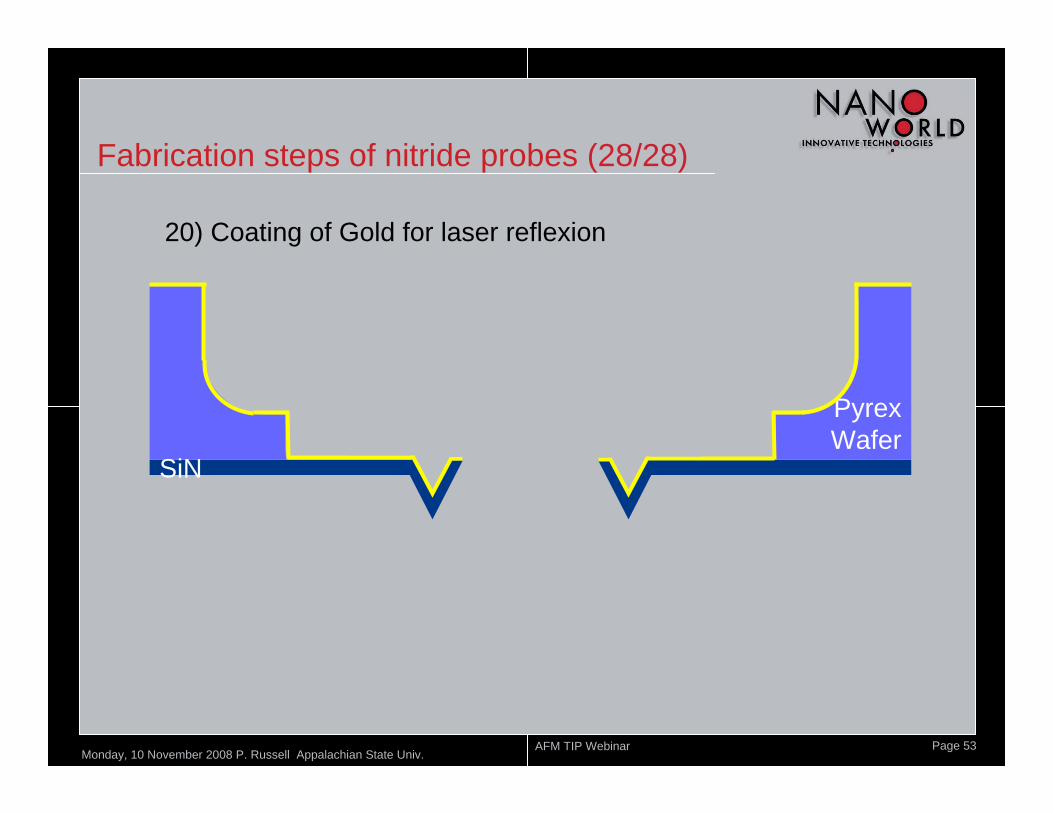
PyrexWafer
SiN
20) Coating of Gold for laser reflexion
Fabrication steps of nitride probes (28/28)
Monday, 10 November 2008 P. Russell Appalachian State Univ. AFM TIP Webinar Page 54
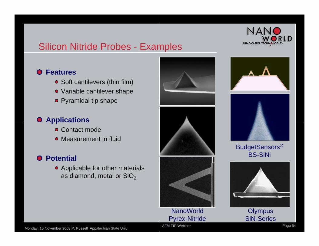
Silicon Nitride Probes - Examples
NanoWorldPyrex-Nitride
BudgetSensors®
BS-SiNi
OlympusSiN-Series
FeaturesSoft cantilevers (thin film)Variable cantilever shapePyramidal tip shape
ApplicationsContact modeMeasurement in fluid
PotentialApplicable for other materials as diamond, metal or SiO2
Monday, 10 November 2008 P. Russell Appalachian State Univ. AFM TIP Webinar Page 55
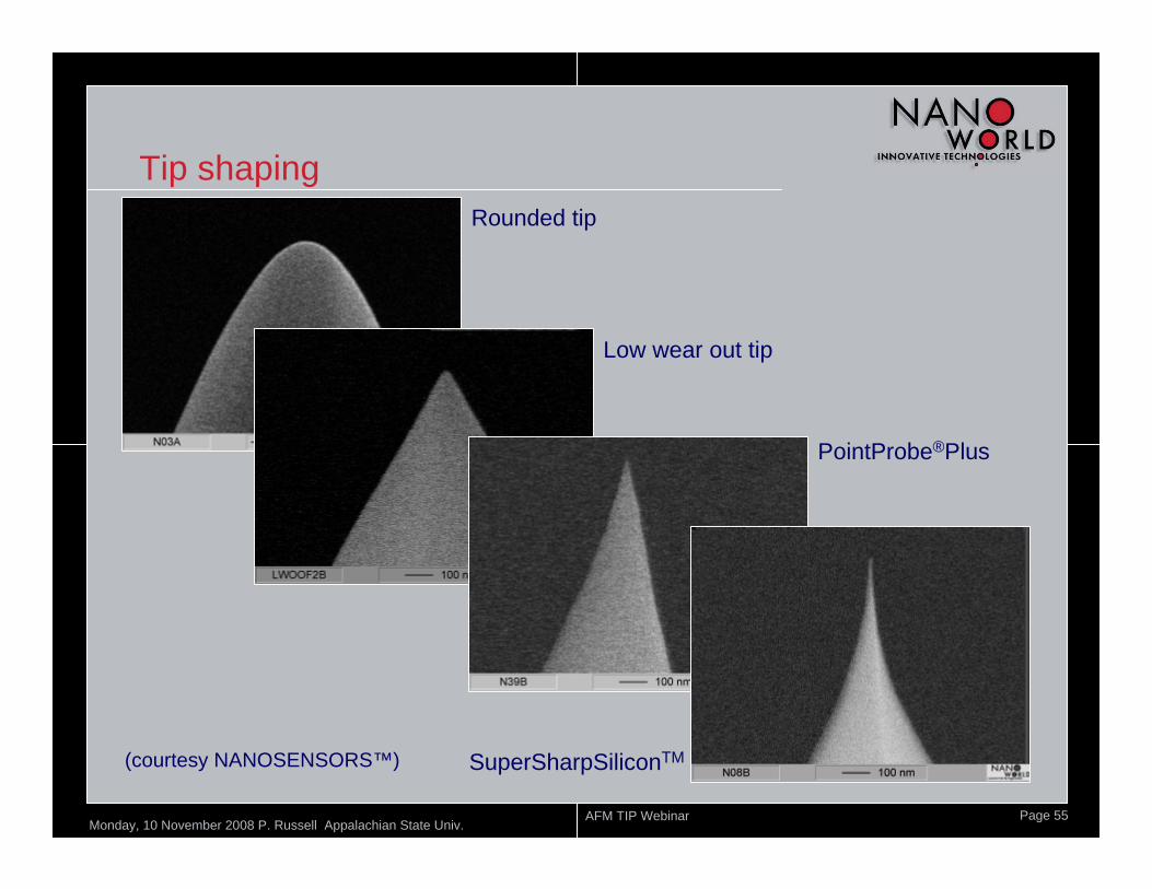
Tip shapingRounded tip
(courtesy NANOSENSORS™)
Low wear out tip
PointProbe®Plus
SuperSharpSiliconTM
Monday, 10 November 2008 P. Russell Appalachian State Univ. AFM TIP Webinar Page 56
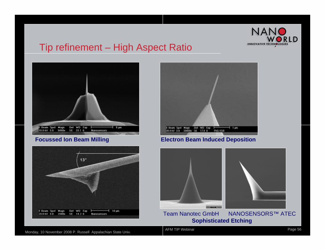
Tip refinement – High Aspect Ratio
Focussed Ion Beam Milling Electron Beam Induced Deposition
Sophisticated EtchingNANOSENSORS™ ATECTeam Nanotec GmbH
Monday, 10 November 2008 P. Russell Appalachian State Univ. AFM TIP Webinar Page 57
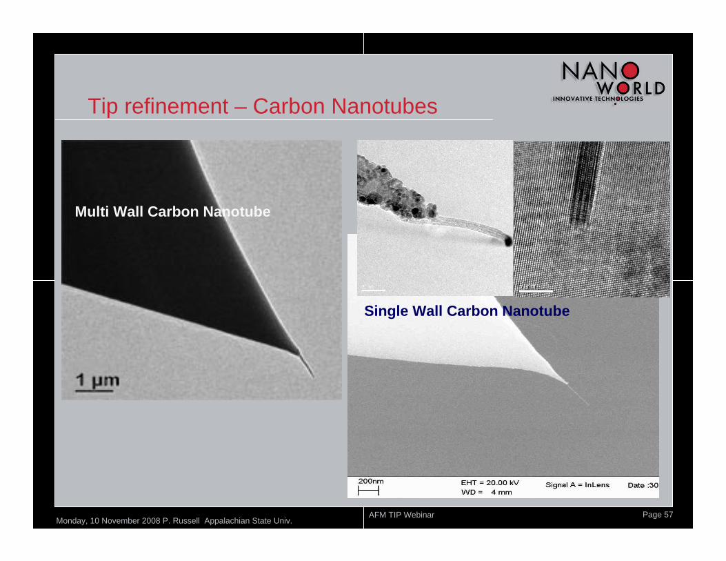
Tip refinement – Carbon Nanotubes
Single Wall Carbon Nanotube
Multi Wall Carbon Nanotube
Monday, 10 November 2008 P. Russell Appalachian State Univ. AFM TIP Webinar Page 58
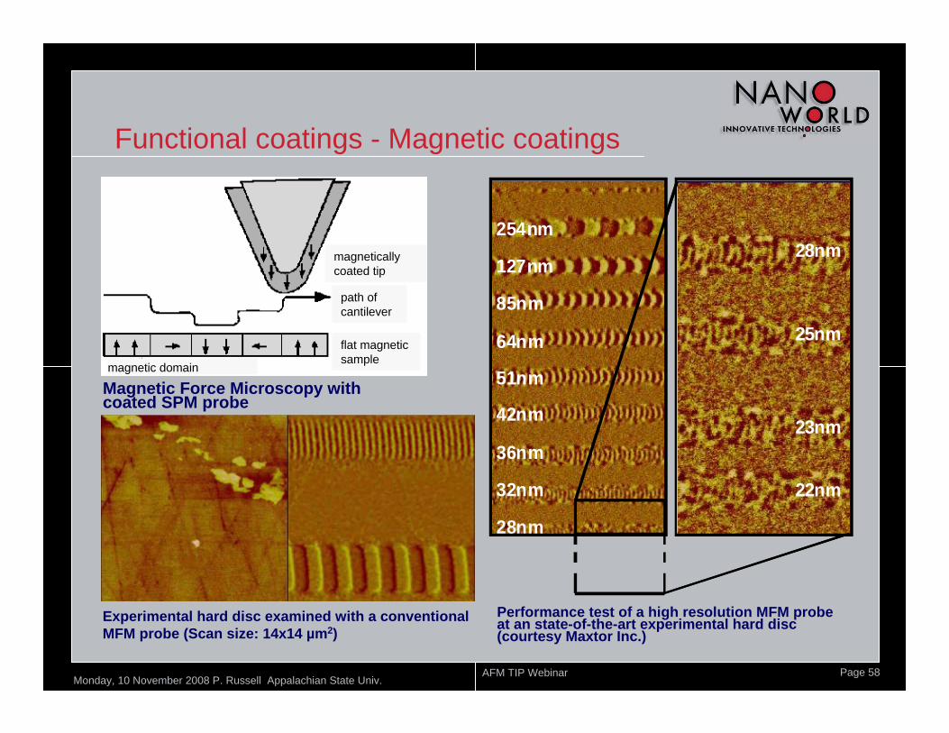
Functional coatings - Magnetic coatings
Experimental hard disc examined with a conventional MFM probe (Scan size: 14x14 µm2)
Performance test of a high resolution MFM probe at an state-of-the-art experimental hard disc (courtesy Maxtor Inc.)
254nm
127nm
85nm
64nm
51nm
42nm
36nm
32nm
28nm
28nm
25nm
23nm
22nm
254nm
127nm
85nm
64nm
51nm
42nm
36nm
32nm
28nm
28nm
25nm
23nm
22nm
Magnetic Force Microscopy with coated SPM probe
magnetically coated tip
path of cantilever
flat magnetic sample
magnetic domain
Monday, 10 November 2008 P. Russell Appalachian State Univ. AFM TIP Webinar Page 59
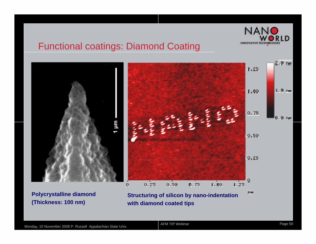
Functional coatings: Diamond Coating
Polycrystalline diamond(Thickness: 100 nm)
Structuring of silicon by nano-indentation with diamond coated tips
Monday, 10 November 2008 P. Russell Appalachian State Univ. AFM TIP Webinar Page 60
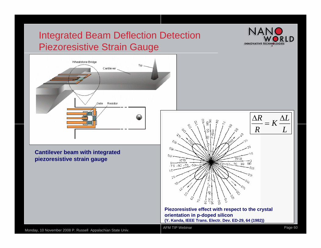
Integrated Beam Deflection DetectionPiezoresistive Strain Gauge
Cantilever beam with integrated piezoresistive strain gauge
LLK
RR Δ=
Δ
Piezoresistive effect with respect to the crystal orientation in p-doped silicon (Y. Kanda, IEEE Trans. Electr. Dev. ED-29, 64 (1982))
Monday, 10 November 2008 P. Russell Appalachian State Univ. AFM TIP Webinar Page 61
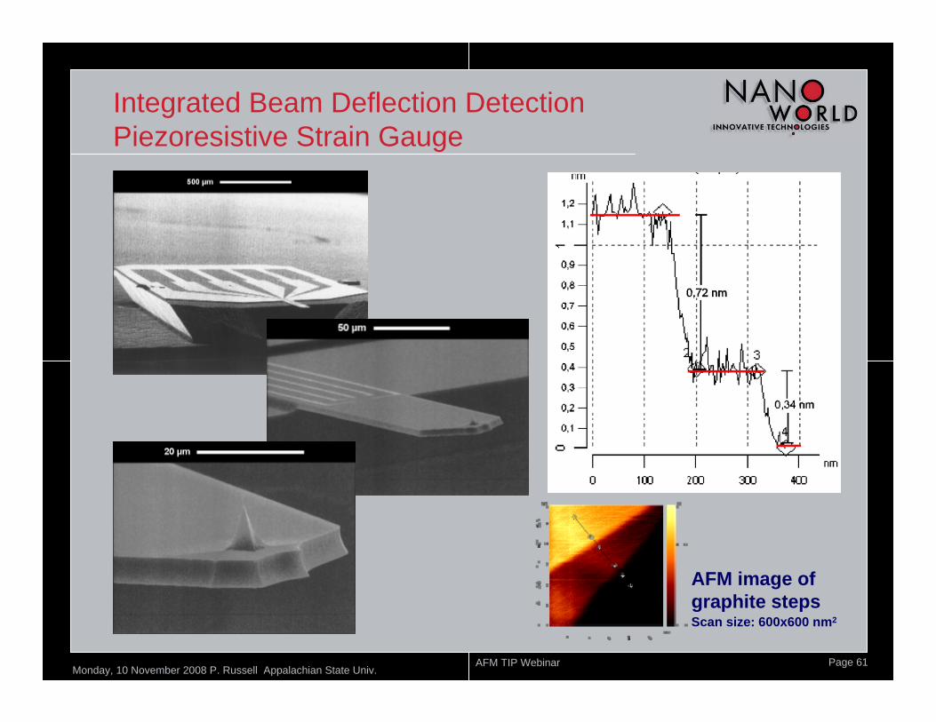
Integrated Beam Deflection DetectionPiezoresistive Strain Gauge
AFM image of graphite stepsScan size: 600x600 nm2
Monday, 10 November 2008 P. Russell Appalachian State Univ. AFM TIP Webinar Page 62
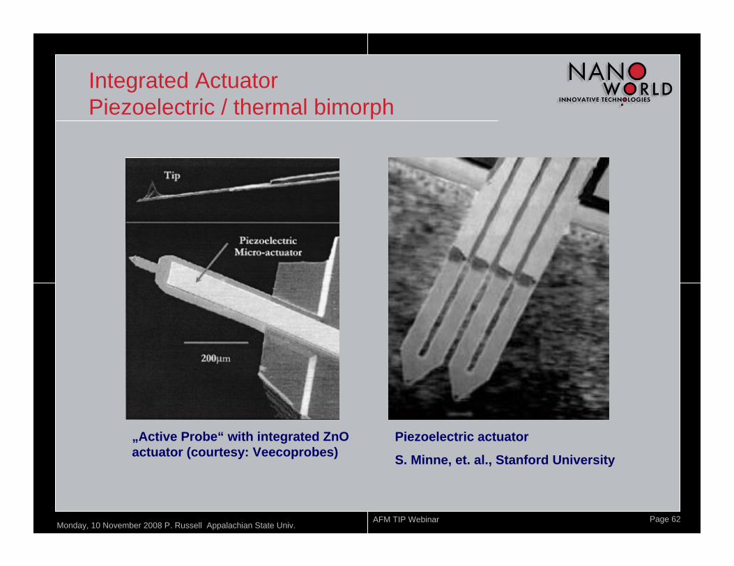
Integrated ActuatorPiezoelectric / thermal bimorph
„Active Probe“ with integrated ZnO actuator (courtesy: Veecoprobes)
Piezoelectric actuator
S. Minne, et. al., Stanford University
Monday, 10 November 2008 P. Russell Appalachian State Univ. AFM TIP Webinar Page 63
Acknowledgement
Thanks to Oliver Krause for use of his excellentTip fabrication slides!