Embed Size (px)
Citation preview

Continued Innovation in ICT
February 2006Page 1
Agilent Bead Probe
Technology
Continued Innovation in ICT
February 2006Page 2
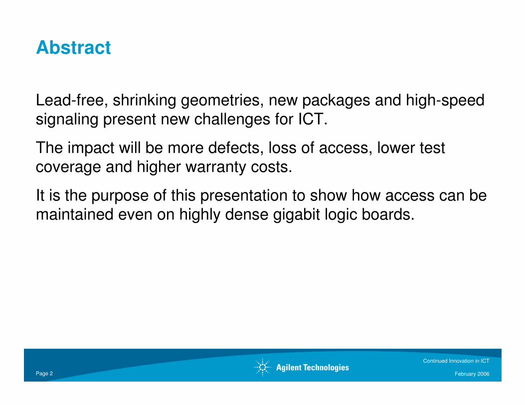
Abstract
Lead-free, shrinking geometries, new packages and high-speed signaling present new challenges for ICT.
The impact will be more defects, loss of access, lower test coverage and higher warranty costs.
It is the purpose of this presentation to show how access can bemaintained even on highly dense gigabit logic boards.
Continued Innovation in ICT
February 2006Page 3
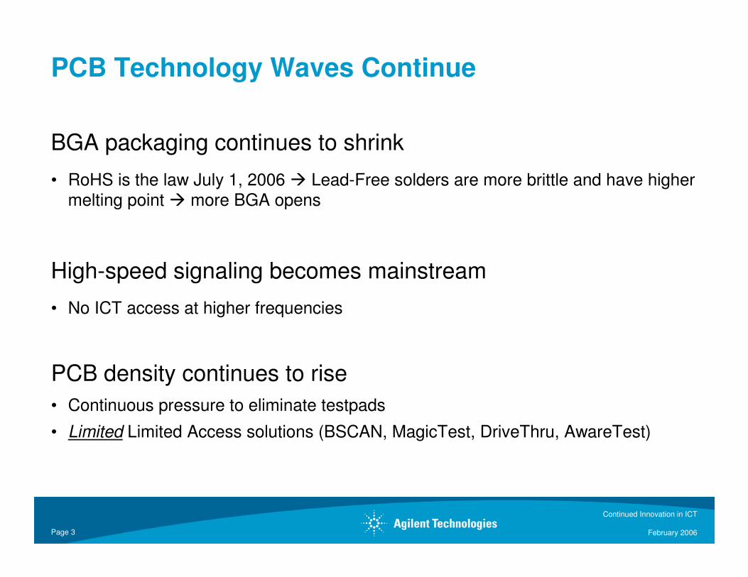
PCB Technology Waves Continue
BGA packaging continues to shrink
• RoHS is the law July 1, 2006 � Lead-Free solders are more brittle and have higher melting point � more BGA opens
High-speed signaling becomes mainstream
• No ICT access at higher frequencies
PCB density continues to rise
• Continuous pressure to eliminate testpads
• Limited Limited Access solutions (BSCAN, MagicTest, DriveThru, AwareTest)
Continued Innovation in ICT
February 2006Page 4
High-Speed Signal Propagation (HSSP) is a
coming “wave” in our industry.
This will create a new class of “defect effects”
we have not seen before.
We need to prepare ourselves for this wave.
High-Speed Signaling Wave
Continued Innovation in ICT
February 2006Page 5
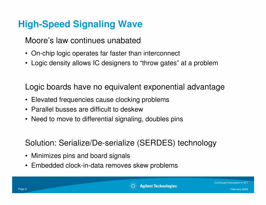
Moore’s law continues unabated
• On-chip logic operates far faster than interconnect
• Logic density allows IC designers to “throw gates” at a problem
Logic boards have no equivalent exponential advantage
• Elevated frequencies cause clocking problems
• Parallel busses are difficult to deskew
• Need to move to differential signaling, doubles pins
Solution: Serialize/De-serialize (SERDES) technology
• Minimizes pins and board signals
• Embedded clock-in-data removes skew problems
High-Speed Signaling Wave
Continued Innovation in ICT
February 2006Page 6
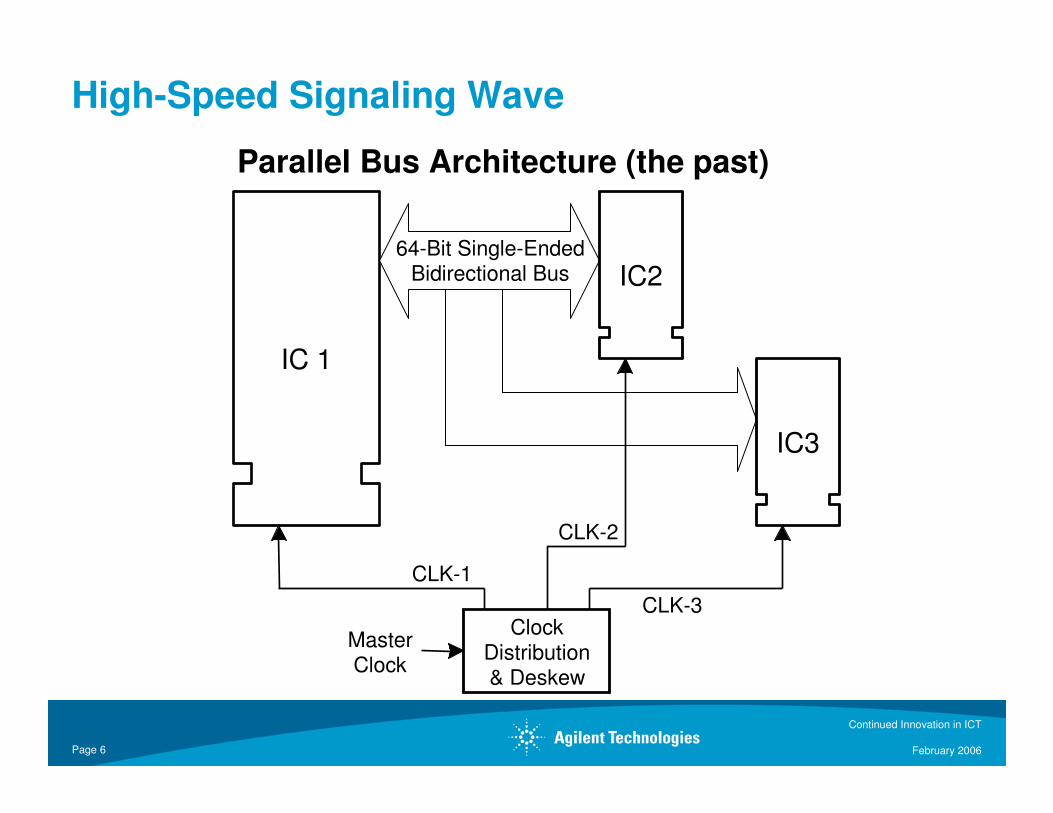
Parallel Bus Architecture (the past)
High-Speed Signaling Wave
IC 1
64-Bit Single-EndedBidirectional Bus IC2
ClockDistribution& Deskew
MasterClock
CLK-1
CLK-2
CLK-3
IC3

Continued Innovation in ICT
February 2006Page 7
Parallel Bus Architecture
High-Speed Signaling Wave
Bit 8
Bit 1
Bit 2
TX RX
Master Clk
Mis
sio
n L
ogic
Mis
sio
n L
ogic

Continued Innovation in ICT
February 2006Page 8
Serial Bus Architecture (the future)
High-Speed Signaling Wave
IC 1
IC2
CLK-1
CLK-2
CLK-3
IC3
8-Bit SerializedDifferential Buses
4-Bit SerializedDifferential Buses
Continued Innovation in ICT
February 2006Page 9
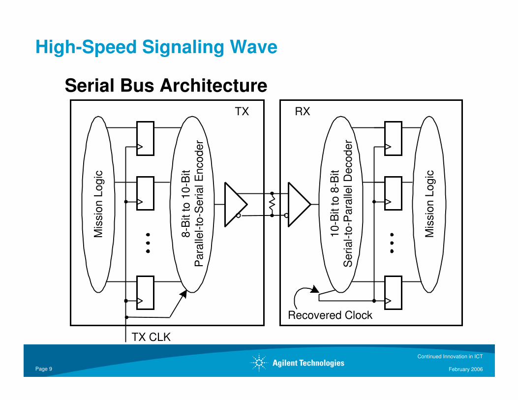
Serial Bus Architecture
High-Speed Signaling Wave
TX RX
TX CLK
Mis
sio
n L
ogic
Mis
sio
n L
ogic
8-B
it to
10-B
itP
ara
llel-to
-Serial E
ncoder
Recovered Clock
10-B
it to
8-B
itS
erial-to
-Para
llel D
ecoder

Continued Innovation in ICT
February 2006Page 10
Interconnect Standards
XAUI
On Chip
PCI 32/33 & 64/66
Chip-to-Chip Local Bus SystemBackplane
CoreConnect SCSI
USB
Serial ATA
IEEE 1394
1Gb Ethernet
CompactPCI
VME
PCI-X 66 & 100
POS-PHY L3/L4
XAUI
3GIO, PCI-Express 2.5Gb/s
RapidIO 3.125Gb/s
3.125Gb/s
Fibre-Channel
InfiniBand 2.5Gb/s
1.5HyperTransport 1.6Gb/s
2nd gen PCI-Express (5-6.25Gb/s)
6Gb/s SATA III
6.25Gb/s double XAUI
VXS Backplane (VITA41)
AdvancedTCA (PICMG 3.x)
GigE Backplane (VITA 31.1)
StarFabric Backplane(PICMG2.17)
Serial Mesh Backplane(PICMG2.20)VME320
1
2.5
2
3
5
6
10Gb Ethernet
CSIX
Flexbus 4
10
Gb/s
Continued Innovation in ICT
February 2006Page 11
High Density PCB Wave
Continuous pressure to eliminate testpads
– Consumes PCB real estate
– Adds to routing complexity
– Used only at ICT, adds no value to board
– No testpads for high speed nets
– Designers perceive risk in adding testpads
– ICT rapidly loses effectiveness with less than 100% access
Limited Limited Access solutions (BSCAN, MagicTest, DriveThru, AwareTest)
– BSCAN requires DFT, expertise, power
– MagicTest and DriveThru address corner cases only
– AwareTest requires X-Ray inspection to perform like a tester

Continued Innovation in ICT
February 2006Page 12
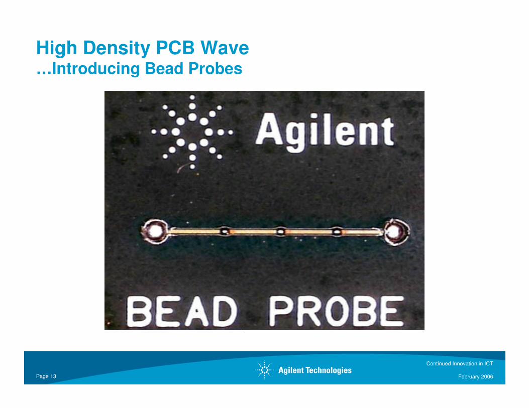
High Density PCB Wave…Introducing Bead Probes
Before: Add probe targets to a board layout and hit
them with probes mounted in a test fixture.
Problem: Probe targets disturb circuit layout.
Solution: Figure out how to
get access without changing
the layout.
New Paradigm: Place probe
targets in a fixture and hit
them with tiny probes
mounted on the board.
No Probe Targets
Probe targets, symmetric and 50 mils apart
Probe Targets, asymmetric and 50 mils apart
Tx
Tx
Tx
Rx
Rx
Rx
Continued Innovation in ICT
February 2006Page 13
High Density PCB Wave…Introducing Bead Probes
Continued Innovation in ICT
February 2006Page 14
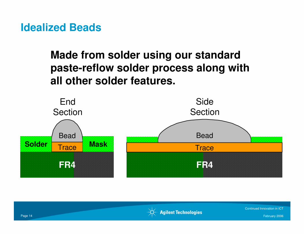
Idealized Beads
Made from solder using our standard
paste-reflow solder process along with
all other solder features.
Bead
FR4
Trace MaskSolder
EndSection
Bead
FR4
SideSection
Trace
Continued Innovation in ICT
February 2006Page 15
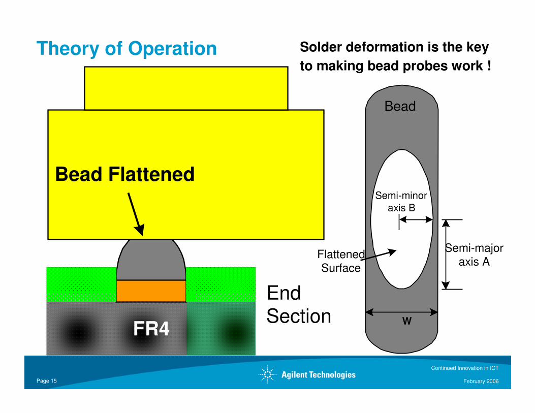
Theory of Operation Solder deformation is the key
to making bead probes work !
FR4
EndSection
Semi-majoraxis A
Semi-minor
axis B
Bead Flattened
FlattenedSurface
W
Bead

Continued Innovation in ICT
February 2006Page 16
Bead Solder Mask and Stencil Stackup
Cu Trace
Cu Trace
Stackup
Solder Mask Opening
Solder Stencil Opening
Stackup
W
L
D

Continued Innovation in ICT
February 2006Page 17
Good view of Bead Probe

Continued Innovation in ICT
February 2006Page 18
TDR of Ideal Trace versus 35 mil target
0.50.0 1.0
38
44
50
32
56
time, nsec
Z_p_id
eal_
5_3_0
Z_p_std
_tp
t_5_3_0
Ideal Trace
With 35 milprobe targetIm
pedance in O
hm
s
Inputdiscontinuity
Outputdiscontinuity
Transit time for 3 inch trace
Continued Innovation in ICT
February 2006Page 19
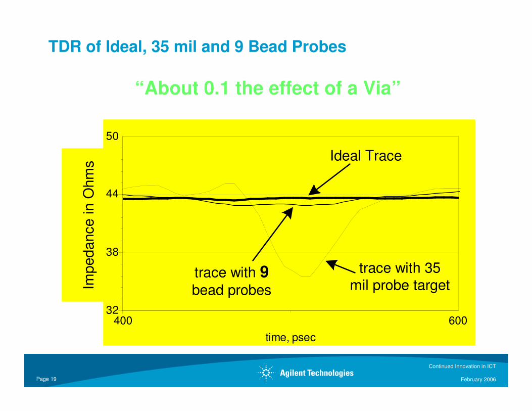
TDR of Ideal, 35 mil and 9 Bead Probes
400 600
38
44
32
50
time, psec
Z_p_id
eal_
5_
3_0
Z_p_
std
_tp
t_5_
3_0
Z_p
_bead
_5_
3_9
Impedance in O
hm
s
Ideal Trace
trace with 35mil probe target
trace with 9bead probes
“About 0.1 the effect of a Via”
Continued Innovation in ICT
February 2006Page 20
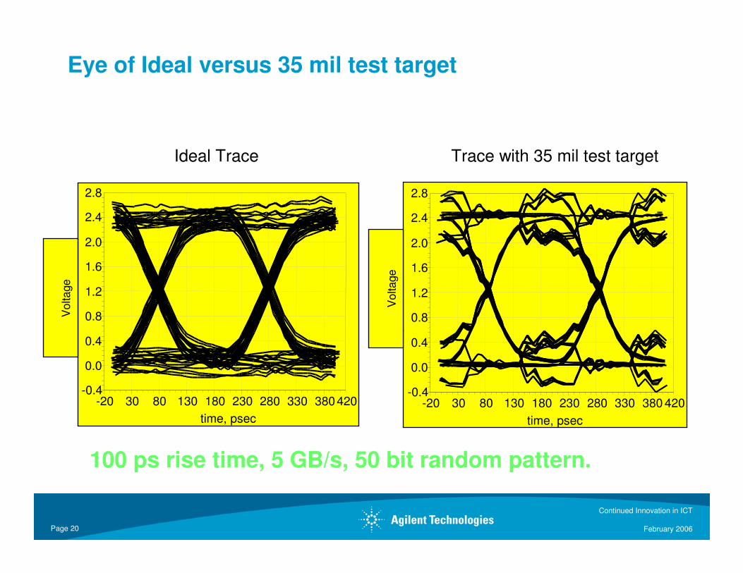
Eye of Ideal versus 35 mil test target
100 ps rise time, 5 GB/s, 50 bit random pattern.
30 80 130 180 230 280 330 380-20 420
0.0
0.4
0.8
1.2
1.6
2.0
2.4
-0.4
2.8
time, psec
p_id
eal_
5_
3_0
Vo
lta
ge
30 80 130 180 230 280 330 380-20 420
0.0
0.4
0.8
1.2
1.6
2.0
2.4
-0.4
2.8
time, psec
p_S
TD
_5
_3
_0
Vo
lta
ge
Ideal Trace Trace with 35 mil test target
Continued Innovation in ICT
February 2006Page 21
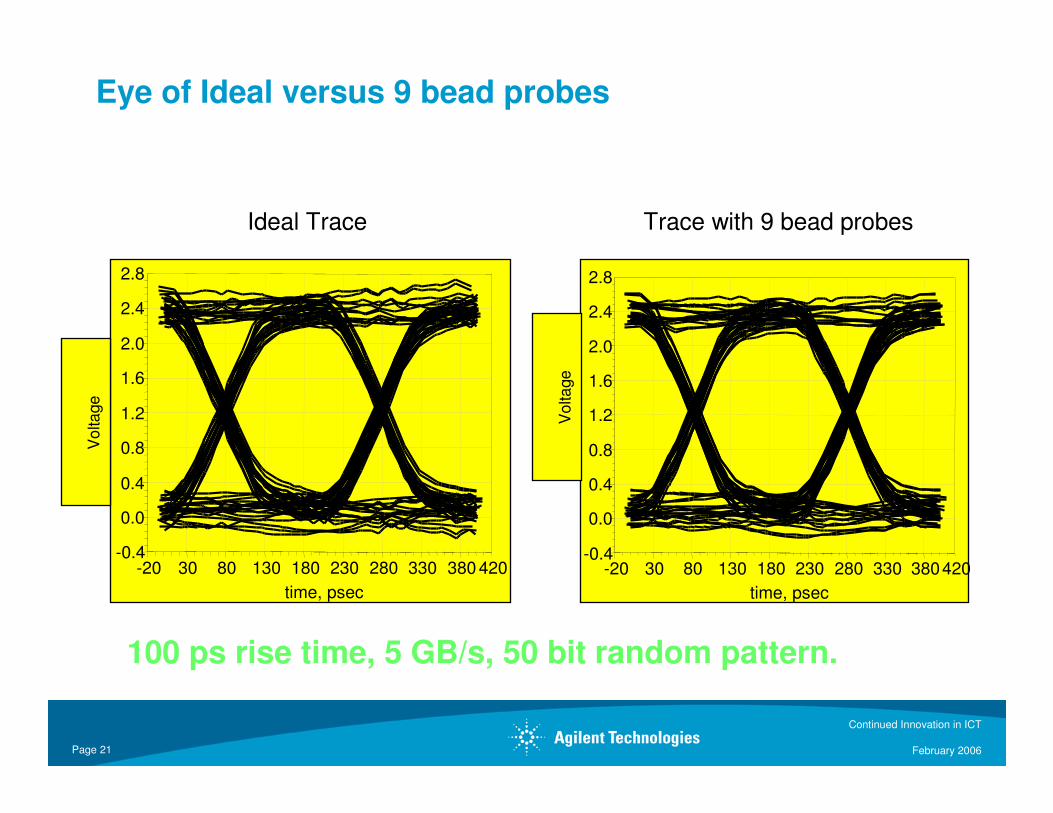
Eye of Ideal versus 9 bead probes
100 ps rise time, 5 GB/s, 50 bit random pattern.
30 80 130 180 230 280 330 380-20 420
0.0
0.4
0.8
1.2
1.6
2.0
2.4
-0.4
2.8
time, psec
p_id
eal_
5_
3_0
Vo
lta
ge
Ideal Trace Trace with 9 bead probes
30 80 130 180 230 280 330 380-20 420
0.0
0.4
0.8
1.2
1.6
2.0
2.4
-0.4
2.8
time, psec
P_B
EA
D_5_
3_
9V
olta
ge

Continued Innovation in ICT
February 2006Page 22
Benefits
Improved test access. Now have a method to add to high speed lines that does not affect signal integrity. Also on dense board have a method to add test coverage.
Uses standard ICT methods.
One the CAD translation software is configured, should be able to use a standard process for bead probe.
Can have multiple bead probe locations for a node.
Can help reduce/eliminate the need for 50mil and 39mil probes, reducing fixture costs and increasing fixture reliability.
Continued Innovation in ICT
February 2006Page 23
Agilent Bead Probe Technology Summary� Simple Design
• No complex signal trace layout design• Board Independence• No risk to signal integrity
� Simple Manufacturing Process• Using existing screen printing and Re-flow processes• No additional process step needed
� Maximize Fault Coverage• Multiple (Alternative) access points on single signal trace• Reliable electrical contact - Bead is self-cleaning (oxide removal) on
contact with Test Probe• Multiple “Re-probing” possible
� Agilent Bead Probe Technology is a proprietary design and manufacturing methodology for Test Probes on PCB signal traces.
� 15 Patents surrounding the design, manufacturability and measurement of electrical signals using this technology has beenfiled.
� Agilent grants the use of Bead Probe Technology on Agilent ICT -free license available
� Visit www.agilent.com/see/beadprobe