Embed Size (px)
Citation preview
Power Generation by Harvesting
Ambient Energy with a
Micro-Electromagnetic Generator
THESIS
James Shields, Captain, USAF
AFIT/GE/ENG/09-42
DEPARTMENT OF THE AIR FORCEAIR UNIVERSITY
AIR FORCE INSTITUTE OF TECHNOLOGY
Wright-Patterson Air Force Base, Ohio
APPROVED FOR PUBLIC RELEASE; DISTRIBUTION UNLIMITED.

The views expressed in this thesis are those of the author and do not reflect theofficial policy or position of the United States Air Force, Department of Defense, orthe United States Government.
AFIT/GE/ENG/09-42
Power Generation by Harvesting
Ambient Energy with a
Micro-Electromagnetic Generator
THESIS
Presented to the Faculty
Department of Electrical and Computer Engineering
Graduate School of Engineering and Management
Air Force Institute of Technology
Air University
Air Education and Training Command
In Partial Fulfillment of the Requirements for the
Degree of Master of Science in Electrical Engineering
James Shields, B.S.C.E.
Captain, USAF
March 2009
APPROVED FOR PUBLIC RELEASE; DISTRIBUTION UNLIMITED.
AFIT/GE/ENG/09-42
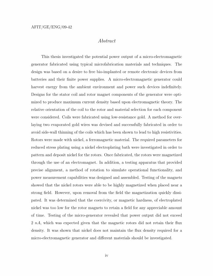
Abstract
This thesis investigated the potential power output of a micro-electromagnetic
generator fabricated using typical microfabrication materials and techniques. The
design was based on a desire to free bio-implanted or remote electronic devices from
batteries and their finite power supplies. A micro-electromagnetic generator could
harvest energy from the ambient environment and power such devices indefinitely.
Designs for the stator coil and rotor magnet components of the generator were opti-
mized to produce maximum current density based upon electromagnetic theory. The
relative orientation of the coil to the rotor and material selection for each component
were considered. Coils were fabricated using low-resistance gold. A method for over-
laying two evaporated gold wires was devised and successfully fabricated in order to
avoid side-wall thinning of the coils which has been shown to lead to high resistivities.
Rotors were made with nickel, a ferromagnetic material. The required parameters for
reduced stress plating using a nickel electroplating bath were investigated in order to
pattern and deposit nickel for the rotors. Once fabricated, the rotors were magnetized
through the use of an electromagnet. In addition, a testing apparatus that provided
precise alignment, a method of rotation to simulate operational functionality, and
power measurement capabilities was designed and assembled. Testing of the magnets
showed that the nickel rotors were able to be highly magnetized when placed near a
strong field. However, upon removal from the field the magnetization quickly dissi-
pated. It was determined that the coercivity, or magnetic hardness, of electroplated
nickel was too low for the rotor magnets to retain a field for any appreciable amount
of time. Testing of the micro-generator revealed that power output did not exceed
2 nA, which was expected given that the magnetic rotors did not retain their flux
density. It was shown that nickel does not maintain the flux density required for a
micro-electromagnetic generator and different materials should be investigated.
iv
Acknowledgements
First and foremost, I would like to express my gratitude and appreciation for my
wife and my children for their patience and support during this thesis effort. I would
also like to formally thank my thesis advisor, Maj. LaVern Starman, and my thesis
committee members, Lt. Col. Ron Coutu, Dr. Michael Durstock and Dr. Nancy
Kelley-Loughnane, for their guidance and insight. In addition, individuals at AFIT,
AFRL/Sensors Directorate, and AFRL/Propulsion Directorate who provided support
with fabrication and testing were invaluable, namely: Rich Johnston, Kevin Leedy,
Capt Kelson Chabak, Paul Cassity, Larry Callahan, and Dr. Zafer Turgut. Finally,
my fellow students were a tremendous asset to discuss ideas and provide critiques
of my work. Thanks to all of them as well: Nick Coleman, Dan Gallagher, Adam
Gubbels, Moe Kossler, Tom Lagoski, Tod Laurvick, Mimi Ledet and Luke Rederus.
James Shields
v
Table of ContentsPage
Abstract . . . . . . . . . . . . . . . . . . . . . . . . . . . . . . . . . . . . . iv
Acknowledgements . . . . . . . . . . . . . . . . . . . . . . . . . . . . . . . v
Table of Contents . . . . . . . . . . . . . . . . . . . . . . . . . . . . . . . . vi
List of Figures . . . . . . . . . . . . . . . . . . . . . . . . . . . . . . . . . ix
List of Tables . . . . . . . . . . . . . . . . . . . . . . . . . . . . . . . . . . xii
List of Abbreviations . . . . . . . . . . . . . . . . . . . . . . . . . . . . . . xiii
I. Introduction . . . . . . . . . . . . . . . . . . . . . . . . . . . . . 11.1 Ambient Energy Harvesting . . . . . . . . . . . . . . . . 1
1.2 Microelectromechanical Systems (MEMS) . . . . . . . . 2
1.3 Problem Overview . . . . . . . . . . . . . . . . . . . . . 41.4 Research Intent . . . . . . . . . . . . . . . . . . . . . . . 51.5 Organization of Thesis . . . . . . . . . . . . . . . . . . . 6
II. Literature Review . . . . . . . . . . . . . . . . . . . . . . . . . . 82.1 From Batteries to Harvesters . . . . . . . . . . . . . . . 82.2 Micro-Scale Energy Harvesting Research . . . . . . . . . 9
2.2.1 Electromagnetic Power Generation . . . . . . . 11
2.2.2 Piezoelectric Power Generation . . . . . . . . . 122.2.3 Electrostatic Power Generation . . . . . . . . . 142.2.4 Previous AFIT Research . . . . . . . . . . . . . 16
2.3 Identified Challenges . . . . . . . . . . . . . . . . . . . . 16
2.4 Chapter Summary . . . . . . . . . . . . . . . . . . . . . 19
III. Methodology and Theory . . . . . . . . . . . . . . . . . . . . . . 20
3.1 Electromagnetic Generators . . . . . . . . . . . . . . . . 20
3.1.1 Theory of Electromagnetic Generators . . . . . 21
3.1.2 Generator Design Parameters . . . . . . . . . . 22
3.2 Magnet Design . . . . . . . . . . . . . . . . . . . . . . . 23
3.2.1 Magnetic Material Selection . . . . . . . . . . . 24
3.2.2 Magnet Layout Design . . . . . . . . . . . . . . 26
3.2.3 Nickel Deposition Process . . . . . . . . . . . . 28
3.2.4 Magnetization of Nickel Deposit . . . . . . . . . 31
vi
Page
3.3 Coil Design . . . . . . . . . . . . . . . . . . . . . . . . . 33
3.3.1 Coil Material Selection . . . . . . . . . . . . . . 333.3.2 Coil Layout . . . . . . . . . . . . . . . . . . . . 34
3.4 Test Structure . . . . . . . . . . . . . . . . . . . . . . . 413.4.1 Rotation Mechanism . . . . . . . . . . . . . . . 413.4.2 Precise Alignment . . . . . . . . . . . . . . . . . 41
3.4.3 Power Output Measurement . . . . . . . . . . . 42
3.5 Chapter Summary . . . . . . . . . . . . . . . . . . . . . 43
IV. Fabrication . . . . . . . . . . . . . . . . . . . . . . . . . . . . . . 444.1 Mask Fabrication and Substrate Selection . . . . . . . . 444.2 Magnet Fabrication . . . . . . . . . . . . . . . . . . . . . 45
4.2.1 Photoresist Characterization . . . . . . . . . . . 454.2.2 Nickel Plating . . . . . . . . . . . . . . . . . . . 47
4.2.3 Magnetization . . . . . . . . . . . . . . . . . . . 57
4.3 Coil Fabrication . . . . . . . . . . . . . . . . . . . . . . . 574.3.1 Runner . . . . . . . . . . . . . . . . . . . . . . . 584.3.2 Dielectric . . . . . . . . . . . . . . . . . . . . . 614.3.3 Coil . . . . . . . . . . . . . . . . . . . . . . . . 61
4.4 Test Structure Assembly . . . . . . . . . . . . . . . . . . 63
4.5 Chapter Summary . . . . . . . . . . . . . . . . . . . . . 66
V. Testing and Results . . . . . . . . . . . . . . . . . . . . . . . . . 68
5.1 Rotor Magnets . . . . . . . . . . . . . . . . . . . . . . . 68
5.2 Stator Coils . . . . . . . . . . . . . . . . . . . . . . . . . 715.3 Testing Apparatus . . . . . . . . . . . . . . . . . . . . . 72
5.4 Micro-Generator . . . . . . . . . . . . . . . . . . . . . . 755.5 Chapter Summary . . . . . . . . . . . . . . . . . . . . . 75
VI. Conclusions . . . . . . . . . . . . . . . . . . . . . . . . . . . . . . 766.1 Scientific Contributions . . . . . . . . . . . . . . . . . . 766.2 Lessons Learned and Recommendations . . . . . . . . . 76
6.2.1 Sample Selection . . . . . . . . . . . . . . . . . 76
6.2.2 LOR for Runner Deposit . . . . . . . . . . . . . 77
6.2.3 Use of a High Precision Rotary Stage . . . . . . 77
6.2.4 Electromagnetic Modeling Tools . . . . . . . . . 77
6.2.5 Magnetic Material Selection . . . . . . . . . . . 77
6.2.6 Turbine Integration, Packaging and Power Con-ditioning . . . . . . . . . . . . . . . . . . . . . . 78
6.2.7 Piezoelectric Research . . . . . . . . . . . . . . 786.3 Conclusion . . . . . . . . . . . . . . . . . . . . . . . . . 79
vii
Page
Appendix A. Supporting Calculations . . . . . . . . . . . . . . . . . . 80
Appendix B. Lithographic Mask Design . . . . . . . . . . . . . . . . . 82
Appendix C. Fabrication Methods . . . . . . . . . . . . . . . . . . . . 90
Appendix D. Experimental Raw Data . . . . . . . . . . . . . . . . . . 94
Bibliography . . . . . . . . . . . . . . . . . . . . . . . . . . . . . . . . . . 98
Vita . . . . . . . . . . . . . . . . . . . . . . . . . . . . . . . . . . . . . . . 100
viii
List of FiguresFigure Page
1.1. Sandia National Labs MEMS Ratchet System . . . . . . . . . . 3
1.2. Penny Sized MEMS Combustion Engine . . . . . . . . . . . . . 4
2.1. Alessandro Volta and the Voltaic Cell . . . . . . . . . . . . . . 8
2.2. Moore’s Law vs. Battery Growth . . . . . . . . . . . . . . . . . 10
2.3. Common Electromagnetic Generator Designs . . . . . . . . . . 11
2.4. Piezoelectric Generator Designs . . . . . . . . . . . . . . . . . . 13
2.5. Coulomb Force Generator Design . . . . . . . . . . . . . . . . . 15
2.6. Coulomb-Damped Resonant Generator Design . . . . . . . . . 15
2.7. MFPG Design . . . . . . . . . . . . . . . . . . . . . . . . . . . 17
3.1. Demonstration of Faraday’s Law . . . . . . . . . . . . . . . . . 21
3.2. MFPG Coil and Magnet Design . . . . . . . . . . . . . . . . . 24
3.3. Rotor Layout - Rectangular Arms . . . . . . . . . . . . . . . . 27
3.4. Rotor Layout - Segmented Toroidal Magnets . . . . . . . . . . 27
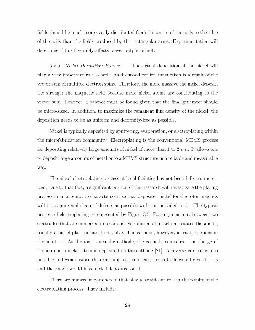
3.5. Nickel Electroplating Process . . . . . . . . . . . . . . . . . . . 29
3.6. Concept Drawing of Generator Design . . . . . . . . . . . . . . 32
3.7. Resistance vs. Coil Turns Plot . . . . . . . . . . . . . . . . . . 35
3.8. Current Path Between Runner and Coil . . . . . . . . . . . . . 36
3.9. Thinning of Coil Sidewalls Due to Runner Deposit . . . . . . . 37
3.10. Original MFPG Coil Layout . . . . . . . . . . . . . . . . . . . 38
3.11. 6 and 12-Turn Arrayed Angled Coil Layout . . . . . . . . . . . 40
3.12. Schematic of Generator Power Testing . . . . . . . . . . . . . . 43
4.1. Spin Curve for AZ P4620 . . . . . . . . . . . . . . . . . . . . . 46
4.2. Exposure Comparison of AZ P4620 Lithography Patterns . . . 47
4.3. Delamination of Sprecher’s Nickel Samples . . . . . . . . . . . 48
4.4. Nickel Electroplating Samples NiStr7b and NiStr8 . . . . . . . 53
ix
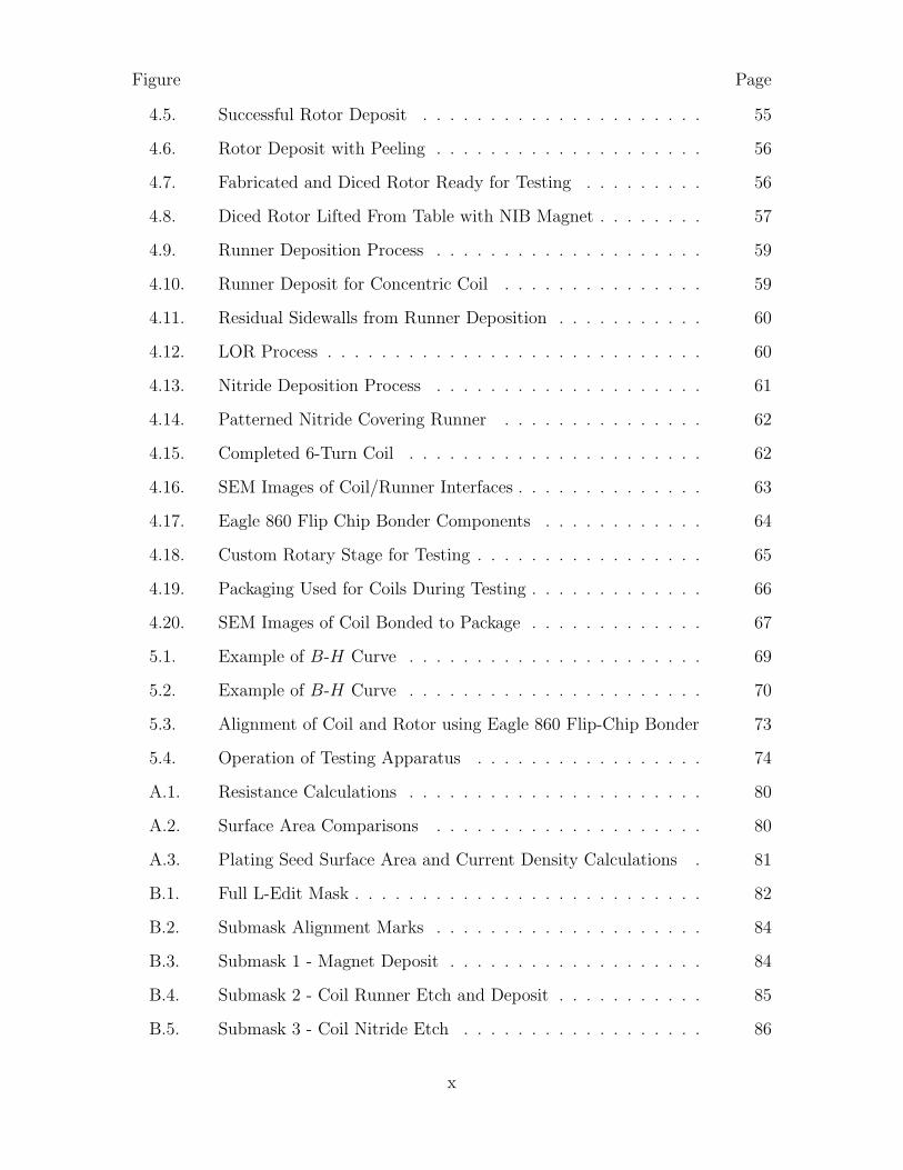
Figure Page
4.5. Successful Rotor Deposit . . . . . . . . . . . . . . . . . . . . . 55
4.6. Rotor Deposit with Peeling . . . . . . . . . . . . . . . . . . . . 56
4.7. Fabricated and Diced Rotor Ready for Testing . . . . . . . . . 56
4.8. Diced Rotor Lifted From Table with NIB Magnet . . . . . . . . 57
4.9. Runner Deposition Process . . . . . . . . . . . . . . . . . . . . 59
4.10. Runner Deposit for Concentric Coil . . . . . . . . . . . . . . . 59
4.11. Residual Sidewalls from Runner Deposition . . . . . . . . . . . 60
4.12. LOR Process . . . . . . . . . . . . . . . . . . . . . . . . . . . . 60
4.13. Nitride Deposition Process . . . . . . . . . . . . . . . . . . . . 61
4.14. Patterned Nitride Covering Runner . . . . . . . . . . . . . . . 62
4.15. Completed 6-Turn Coil . . . . . . . . . . . . . . . . . . . . . . 62
4.16. SEM Images of Coil/Runner Interfaces . . . . . . . . . . . . . . 63
4.17. Eagle 860 Flip Chip Bonder Components . . . . . . . . . . . . 64
4.18. Custom Rotary Stage for Testing . . . . . . . . . . . . . . . . . 65
4.19. Packaging Used for Coils During Testing . . . . . . . . . . . . . 66
4.20. SEM Images of Coil Bonded to Package . . . . . . . . . . . . . 67
5.1. Example of B-H Curve . . . . . . . . . . . . . . . . . . . . . . 69
5.2. Example of B-H Curve . . . . . . . . . . . . . . . . . . . . . . 70
5.3. Alignment of Coil and Rotor using Eagle 860 Flip-Chip Bonder 73
5.4. Operation of Testing Apparatus . . . . . . . . . . . . . . . . . 74
A.1. Resistance Calculations . . . . . . . . . . . . . . . . . . . . . . 80
A.2. Surface Area Comparisons . . . . . . . . . . . . . . . . . . . . 80
A.3. Plating Seed Surface Area and Current Density Calculations . 81
B.1. Full L-Edit Mask . . . . . . . . . . . . . . . . . . . . . . . . . . 82
B.2. Submask Alignment Marks . . . . . . . . . . . . . . . . . . . . 84
B.3. Submask 1 - Magnet Deposit . . . . . . . . . . . . . . . . . . . 84
B.4. Submask 2 - Coil Runner Etch and Deposit . . . . . . . . . . . 85
B.5. Submask 3 - Coil Nitride Etch . . . . . . . . . . . . . . . . . . 86
x
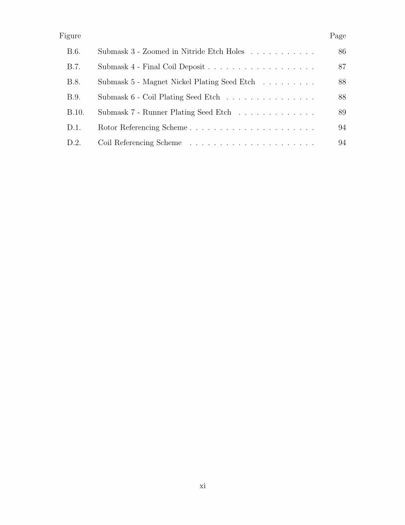
Figure Page
B.6. Submask 3 - Zoomed in Nitride Etch Holes . . . . . . . . . . . 86
B.7. Submask 4 - Final Coil Deposit . . . . . . . . . . . . . . . . . . 87
B.8. Submask 5 - Magnet Nickel Plating Seed Etch . . . . . . . . . 88
B.9. Submask 6 - Coil Plating Seed Etch . . . . . . . . . . . . . . . 88
B.10. Submask 7 - Runner Plating Seed Etch . . . . . . . . . . . . . 89
D.1. Rotor Referencing Scheme . . . . . . . . . . . . . . . . . . . . . 94
D.2. Coil Referencing Scheme . . . . . . . . . . . . . . . . . . . . . 94
xi
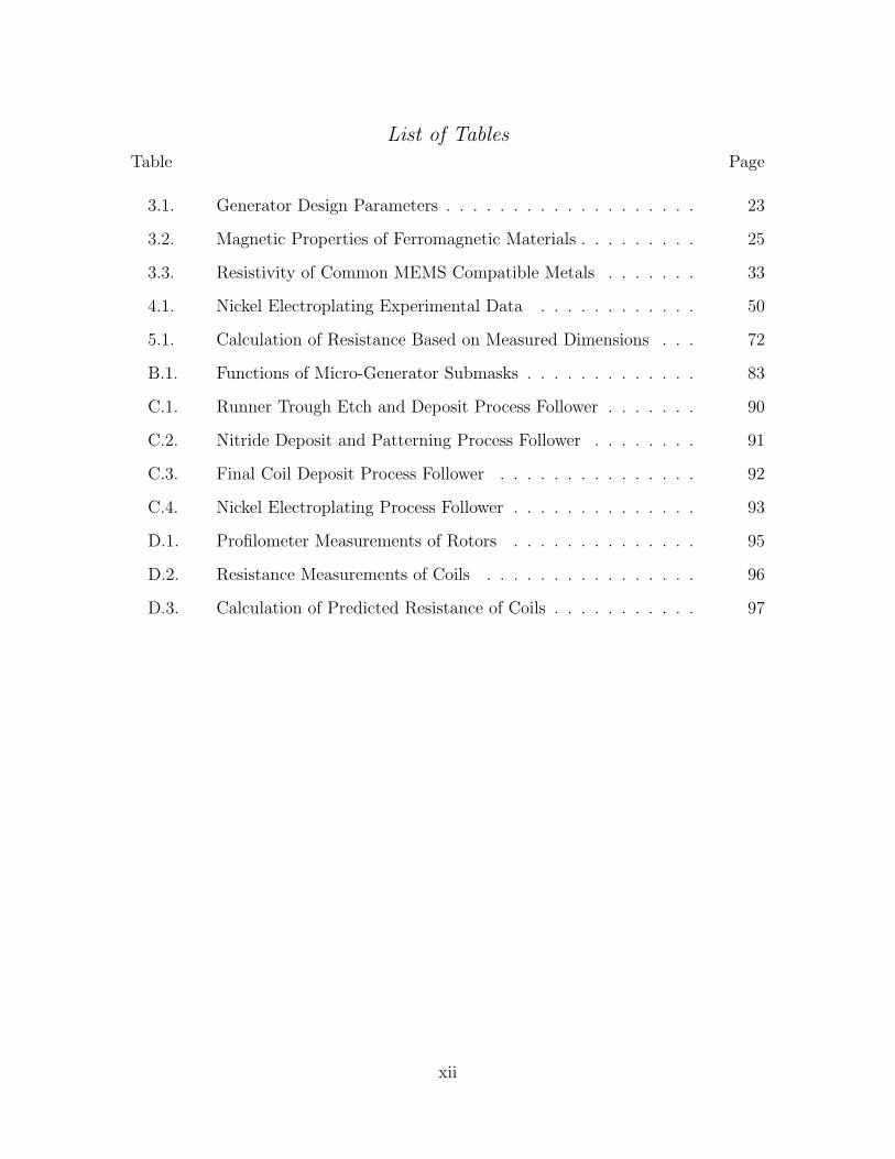
List of TablesTable Page
3.1. Generator Design Parameters . . . . . . . . . . . . . . . . . . . 23
3.2. Magnetic Properties of Ferromagnetic Materials . . . . . . . . . 25
3.3. Resistivity of Common MEMS Compatible Metals . . . . . . . 33
4.1. Nickel Electroplating Experimental Data . . . . . . . . . . . . 50
5.1. Calculation of Resistance Based on Measured Dimensions . . . 72
B.1. Functions of Micro-Generator Submasks . . . . . . . . . . . . . 83
C.1. Runner Trough Etch and Deposit Process Follower . . . . . . . 90
C.2. Nitride Deposit and Patterning Process Follower . . . . . . . . 91
C.3. Final Coil Deposit Process Follower . . . . . . . . . . . . . . . 92
C.4. Nickel Electroplating Process Follower . . . . . . . . . . . . . . 93
D.1. Profilometer Measurements of Rotors . . . . . . . . . . . . . . 95
D.2. Resistance Measurements of Coils . . . . . . . . . . . . . . . . 96
D.3. Calculation of Predicted Resistance of Coils . . . . . . . . . . . 97
xii
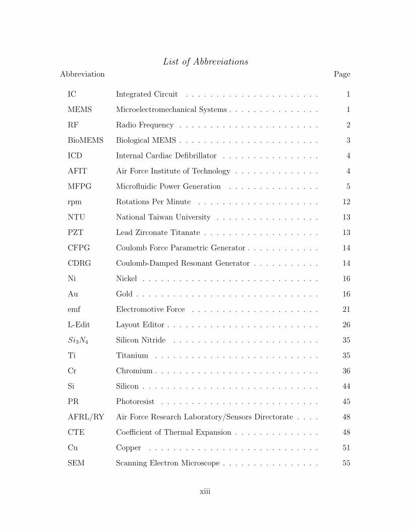
List of AbbreviationsAbbreviation Page
IC Integrated Circuit . . . . . . . . . . . . . . . . . . . . . . 1
MEMS Microelectromechanical Systems . . . . . . . . . . . . . . . 1
RF Radio Frequency . . . . . . . . . . . . . . . . . . . . . . . 2
BioMEMS Biological MEMS . . . . . . . . . . . . . . . . . . . . . . . 3
ICD Internal Cardiac Defibrillator . . . . . . . . . . . . . . . . 4
AFIT Air Force Institute of Technology . . . . . . . . . . . . . . 4
MFPG Microfluidic Power Generation . . . . . . . . . . . . . . . 5
rpm Rotations Per Minute . . . . . . . . . . . . . . . . . . . . 12
NTU National Taiwan University . . . . . . . . . . . . . . . . . 13
PZT Lead Zirconate Titanate . . . . . . . . . . . . . . . . . . . 13
CFPG Coulomb Force Parametric Generator . . . . . . . . . . . . 14
CDRG Coulomb-Damped Resonant Generator . . . . . . . . . . . 14
Ni Nickel . . . . . . . . . . . . . . . . . . . . . . . . . . . . . 16
Au Gold . . . . . . . . . . . . . . . . . . . . . . . . . . . . . . 16
emf Electromotive Force . . . . . . . . . . . . . . . . . . . . . 21
L-Edit Layout Editor . . . . . . . . . . . . . . . . . . . . . . . . . 26
Si3N4 Silicon Nitride . . . . . . . . . . . . . . . . . . . . . . . . 35
Ti Titanium . . . . . . . . . . . . . . . . . . . . . . . . . . . 35
Cr Chromium . . . . . . . . . . . . . . . . . . . . . . . . . . . 36
Si Silicon . . . . . . . . . . . . . . . . . . . . . . . . . . . . . 44
PR Photoresist . . . . . . . . . . . . . . . . . . . . . . . . . . 45
AFRL/RY Air Force Research Laboratory/Sensors Directorate . . . . 48
CTE Coefficient of Thermal Expansion . . . . . . . . . . . . . . 48
Cu Copper . . . . . . . . . . . . . . . . . . . . . . . . . . . . 51
SEM Scanning Electron Microscope . . . . . . . . . . . . . . . . 55
xiii
Abbreviation Page
NIB Neodymium Iron Boron . . . . . . . . . . . . . . . . . . . 57
RIE Reactive Ion Etch . . . . . . . . . . . . . . . . . . . . . . 58
PECVD Plasma Enhanced Chemical Vapor Deposition . . . . . . . 58
LOR Lift Off Resist . . . . . . . . . . . . . . . . . . . . . . . . 59
VSM Vibrating Sample Magnetometer . . . . . . . . . . . . . . 70
AFRL/RZ Air Force Research Laboratory/Propulsion Directorate . . 70
PLD Pulse Laser Deposition . . . . . . . . . . . . . . . . . . . . 78
xiv
Power Generation by Harvesting
Ambient Energy with a
Micro-Electromagnetic Generator
I. Introduction
Can you think of a person that does not make use of a mobile electronic device
(wireless phone, MP3 player, garage door opener, pacemaker, etc.)? It is very unlikely.
Mobile electronics are an essential part of our current society. This is due, in no small
part, to continuing advances in integrated circuit (IC) and microelectromechanical
systems (MEMS) technology. Engineers paradoxically provide more capability and
computing power even as the actual electronic devices become smaller. Typically,
as these devices become smaller and more powerful, unhampered mobility tends to
become a requirement, or at least highly desired.
For an electronic device to be mobile, however, a portable power source is re-
quired. For the majority of modern day mobile electronics, that power source is
provided by a battery which inherently has severe drawbacks: mass, volume and
most importantly, a finite power supply. Recently, much research has been applied
in the MEMS domain to discover methods of harvesting energy from the ambient
environment of these miniaturized mobile systems and converting that energy to elec-
tricity to power the circuitry of the device, thus eliminating the need for batteries and
their shortcomings. This thesis will investigate one such method of harvesting that
ambient energy.
1.1 Ambient Energy Harvesting
Energy sources to be potentially harvested and converted to electrical energy
include solar, acoustic, thermal and any kinetic motion. Kinetic energy sources are
numerous and can be harvested with a number of different methods. Within coal
plants, nuclear plants, and hydroelectric dams the kinetic energy of the moving steam
1
or water is converted through the use of an electromagnetic generator and turbine. A
company from Germany, EnOcean GmbH, created a wireless light switch that gleans
the energy required to transmit the radio frequency (RF) signal to the lights from the
kinetic motion of pushing in the switch [1].
Of course the potential sources of ambient energy depend entirely on the in-
tended environment of the device to be used. If a device does not experience signifi-
cant exposure to light, then solar harvesting is not a viable option. The environment
that the electronic system is designed to operate in must be analyzed in order to
identify energy sources that could be harvested. With reported growth rates as high
as 78% within the energy harvesting market [1], it appears that there are numerous
opportunities to move away from a battery solution and look to harvesting untapped
ambient energy.
1.2 Microelectromechanical Systems (MEMS)
In recent years numerous gaming systems have introduced motion-sensitive con-
trollers through the use of a MEMS accelerometer. MEMS technology is often asso-
ciated with microelectronics, but there are distinct differences. This misconception is
most likely due to the fact that they are both typically manufactured using the same
micro and nano-lithographic processes and are often reliant upon one another within
a fielded device. While microelectronics make use of silicon and other semiconduc-
tor materials to manipulate the flow of electrons and thereby process information,
MEMS use those materials to create transducers or minute physical mechanisms such
as mirrors, latches, or gears such as those shown in Figure 1.1.
A transducer is defined as “a device that is actuated by power from one system
and supplies power usually in another form to a second system” [3]. By acting as a
transducer, MEMS provide the capability to transfer information between the phys-
ical world and the microelectronic world. When a MEMS device is used to transfer
information from the electronic world to the physical, then it is referred to as an actu-
ator. If the MEMS device is used to transfer information from the physical world to
2
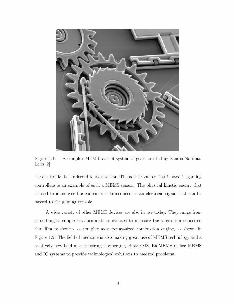
Figure 1.1: A complex MEMS ratchet system of gears created by Sandia NationalLabs [2].
the electronic, it is referred to as a sensor. The accelerometer that is used in gaming
controllers is an example of such a MEMS sensor. The physical kinetic energy that
is used to maneuver the controller is transduced to an electrical signal that can be
passed to the gaming console.
A wide variety of other MEMS devices are also in use today. They range from
something as simple as a beam structure used to measure the stress of a deposited
thin film to devices as complex as a penny-sized combustion engine, as shown in
Figure 1.2. The field of medicine is also making great use of MEMS technology and a
relatively new field of engineering is emerging–BioMEMS. BioMEMS utilize MEMS
and IC systems to provide technological solutions to medical problems.
3
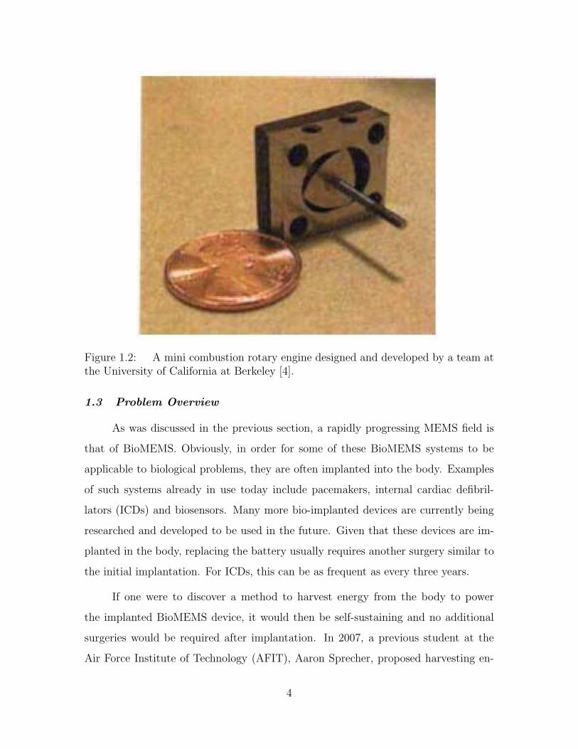
Figure 1.2: A mini combustion rotary engine designed and developed by a team atthe University of California at Berkeley [4].
1.3 Problem Overview
As was discussed in the previous section, a rapidly progressing MEMS field is
that of BioMEMS. Obviously, in order for some of these BioMEMS systems to be
applicable to biological problems, they are often implanted into the body. Examples
of such systems already in use today include pacemakers, internal cardiac defibril-
lators (ICDs) and biosensors. Many more bio-implanted devices are currently being
researched and developed to be used in the future. Given that these devices are im-
planted in the body, replacing the battery usually requires another surgery similar to
the initial implantation. For ICDs, this can be as frequent as every three years.
If one were to discover a method to harvest energy from the body to power
the implanted BioMEMS device, it would then be self-sustaining and no additional
surgeries would be required after implantation. In 2007, a previous student at the
Air Force Institute of Technology (AFIT), Aaron Sprecher, proposed harvesting en-
4
ergy from blood flow similar to the way a hydroelectric dam harvests energy from the
flow of water [5]. His design used a micro-sized electromagnetic generator to convert
the energy of blood flow to electricity. Sprecher was unable to completely fabricate
his design within the time frame he was allotted, but was able to propose a de-
sign, perform theoretical calculations, and begin characterizing fabrication methods.
Currently, there are a number of unanswered questions about his proposed design.
Primarily, how much power can one realistically harvest using his Microfluidic Power
Generation (MFPG) approach? Will his predicted estimates match the experimen-
tal results? What parameters are most influential in optimizing the efficiency of the
electromagnetic generator? Is it feasible to fabricate the device as it was originally
envisioned?
1.4 Research Intent
The goal of this thesis is to further investigate the feasibility of using a micro-
electromagnetic generator to harvest energy from fluid flow and answer those questions
that were proposed in the previous section. With the rapid advancements that are
occurring in MEMS technology, it seems logical to believe that an electromagnetic
generator design that is extensively used at the macro scale should be achievable
at the micro scale as well. However, very little research has been accomplished to
characterize electromagnetic generators at the micro scale, therefore, it is the intent
of this thesis to fabricate the micro-electromagnetic generator portion of the MFPG
design and thereby characterize the potential power output of such a device.
The original MFPG design included numerous components and assembly was
complex. This thesis will focus on the fabrication and design of the generator portion
only, thereby reducing complexity and allowing for full characterization of the poten-
tial power output. The following objectives will lead to such a characterization of the
micro-electromagnetic generator:
1. Design and fabricate a MEMS-compatible magnetic rotor for a micro-generator.
5
2. Design and fabricate a MEMS-compatible stator coil that minimizes resistance
and maximizes power output.
3. Determine how to best polarize the rotor magnet structures.
4. Design a simple testing apparatus for the generator that allows for power output
measurements.
5. Perform the characterization tests for varying generator designs and parameters.
1.5 Organization of Thesis
This thesis will be organized in the following manner:
Chapter 1 - Introduction Provide an introduction to this thesis effort by pointing
out the need to move away from batteries for mobile devices, provide an overview
of MEMS engineering, identify the questions that need to be answered before
fully fabricating the MFPG design, and lay out the goals of this effort.
Chapter 2 - Literature Review Discuss the current research in micro-power gen-
eration that applies to a bio-implanted system and the challenges associated
with it. Provide background information of previous micro-generator research
accomplished at AFIT.
Chapter 3 - Methodology and Theory Explicitly detail the problem solving ap-
proach for designing a micro-generator. Discuss the theory upon which proposed
layouts and material selection was based. Present optimized designs and discuss
testing requirements.
Chapter 4 - Fabrication Discuss the fabrication process of the rotor magnet, sta-
tor coil and testing apparatus. Present the characterization process for any
steps that required characterization.
Chapter 5 - Testing and Results Discuss results of testing of the micro-generator
and identify trends.
6
Chapter 6 - Conclusions Provide recommendations for future research and discuss
the scientific contributions made during this effort.
Appendix A - Supporting Calculations Calculations performed for this thesis
effort.
Appendix B - Lithographic Mask Design Provides details and images of the
lithographic mask used for the micro-generator.
Appendix C - Fabrication Methods Compilation of process followers and fabri-
cation methods used.
Appendix D - Experimental Raw Data Collection of the raw data collected from
the micro-generator measurements and testing.
7
II. Literature Review
This chapter will explore some of the state-of-the-art techniques of micro-power har-
vesting and their associated research; focusing on the techniques that could potentially
be used with bio-implanted systems. In addition, the research that was previously
conducted at AFIT will be discussed and analyzed. Finally a summary of the ongoing
challenges associated with this field of research will be presented.
2.1 From Batteries to Harvesters
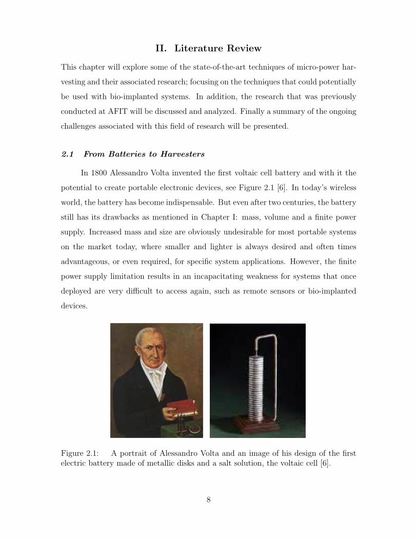
In 1800 Alessandro Volta invented the first voltaic cell battery and with it the
potential to create portable electronic devices, see Figure 2.1 [6]. In today’s wireless
world, the battery has become indispensable. But even after two centuries, the battery
still has its drawbacks as mentioned in Chapter I: mass, volume and a finite power
supply. Increased mass and size are obviously undesirable for most portable systems
on the market today, where smaller and lighter is always desired and often times
advantageous, or even required, for specific system applications. However, the finite
power supply limitation results in an incapacitating weakness for systems that once
deployed are very difficult to access again, such as remote sensors or bio-implanted
devices.
Figure 2.1: A portrait of Alessandro Volta and an image of his design of the firstelectric battery made of metallic disks and a salt solution, the voltaic cell [6].
8
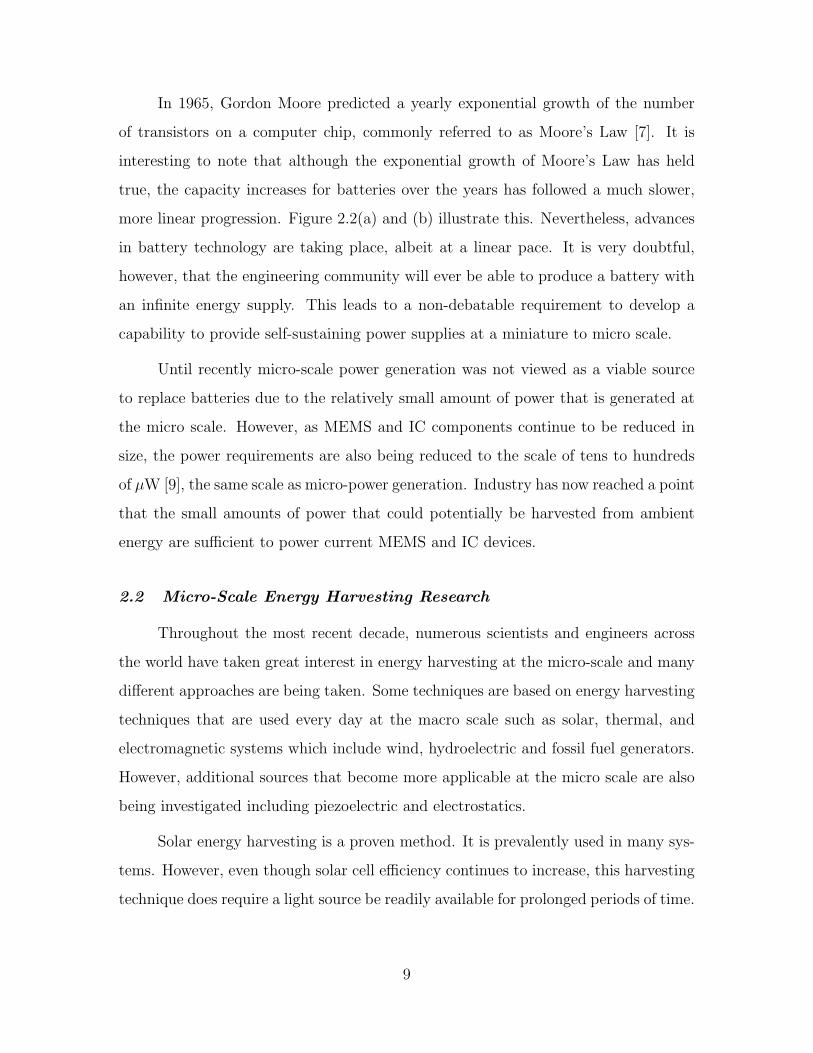
In 1965, Gordon Moore predicted a yearly exponential growth of the number
of transistors on a computer chip, commonly referred to as Moore’s Law [7]. It is
interesting to note that although the exponential growth of Moore’s Law has held
true, the capacity increases for batteries over the years has followed a much slower,
more linear progression. Figure 2.2(a) and (b) illustrate this. Nevertheless, advances
in battery technology are taking place, albeit at a linear pace. It is very doubtful,
however, that the engineering community will ever be able to produce a battery with
an infinite energy supply. This leads to a non-debatable requirement to develop a
capability to provide self-sustaining power supplies at a miniature to micro scale.
Until recently micro-scale power generation was not viewed as a viable source
to replace batteries due to the relatively small amount of power that is generated at
the micro scale. However, as MEMS and IC components continue to be reduced in
size, the power requirements are also being reduced to the scale of tens to hundreds
of µW [9], the same scale as micro-power generation. Industry has now reached a point
that the small amounts of power that could potentially be harvested from ambient
energy are sufficient to power current MEMS and IC devices.
2.2 Micro-Scale Energy Harvesting Research
Throughout the most recent decade, numerous scientists and engineers across
the world have taken great interest in energy harvesting at the micro-scale and many
different approaches are being taken. Some techniques are based on energy harvesting
techniques that are used every day at the macro scale such as solar, thermal, and
electromagnetic systems which include wind, hydroelectric and fossil fuel generators.
However, additional sources that become more applicable at the micro scale are also
being investigated including piezoelectric and electrostatics.
Solar energy harvesting is a proven method. It is prevalently used in many sys-
tems. However, even though solar cell efficiency continues to increase, this harvesting
technique does require a light source be readily available for prolonged periods of time.
9
(a) Moore’s Law Graph [7]
(b) Battery Capacity Graph [8]
Figure 2.2: (a) Moore’s Law predicts an exponential growth in transistor technol-ogy; a trend that has been followed since the 1970s. (b) Battery capacity growth hasfollowed a much more linear trend. Note the logarithmic scale of transistor growthcompared to the linear scale of battery capacity growth.
10
For most personal electronics and all bio-implanted systems this is not an option that
would be applicable.
Thermal energy harvesting requires that thermal gradients be present. Again,
although thermal gradients are available in some environments, this is not a viable
option for bio-implanted devices given that there are no consistent and substantial
temperature gradients in the body. Therefore, electromagnetic, piezoelectric, and
electrostatic energy sources are the potential solutions for bio-implanted devices and
each will now be investigated in depth in the subsequent sections [10].
2.2.1 Electromagnetic Power Generation. Electromagnetic generators at
the macro scale are well understood energy sources. They have been used for decades
in hydroelectric dams, fossil fuel plants and wind generators. The interest in the use
of electromagnetic generators at the micro scale is largely based on the high power
density and efficiency found in the macro scale systems. In fact, it has been shown
that the flux density available from a permanent magnet is independent of its size
and that current densities might even benefit from increased surface area and reduced
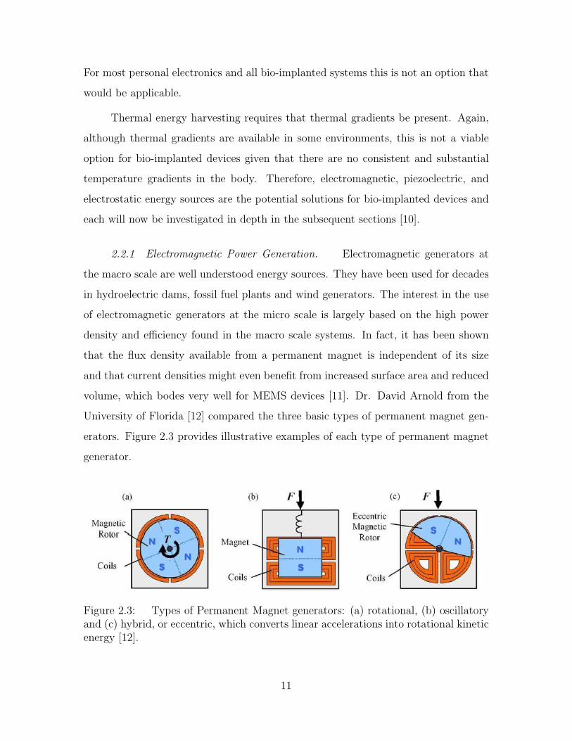
volume, which bodes very well for MEMS devices [11]. Dr. David Arnold from the
University of Florida [12] compared the three basic types of permanent magnet gen-
erators. Figure 2.3 provides illustrative examples of each type of permanent magnet
generator.
Figure 2.3: Types of Permanent Magnet generators: (a) rotational, (b) oscillatoryand (c) hybrid, or eccentric, which converts linear accelerations into rotational kineticenergy [12].
11
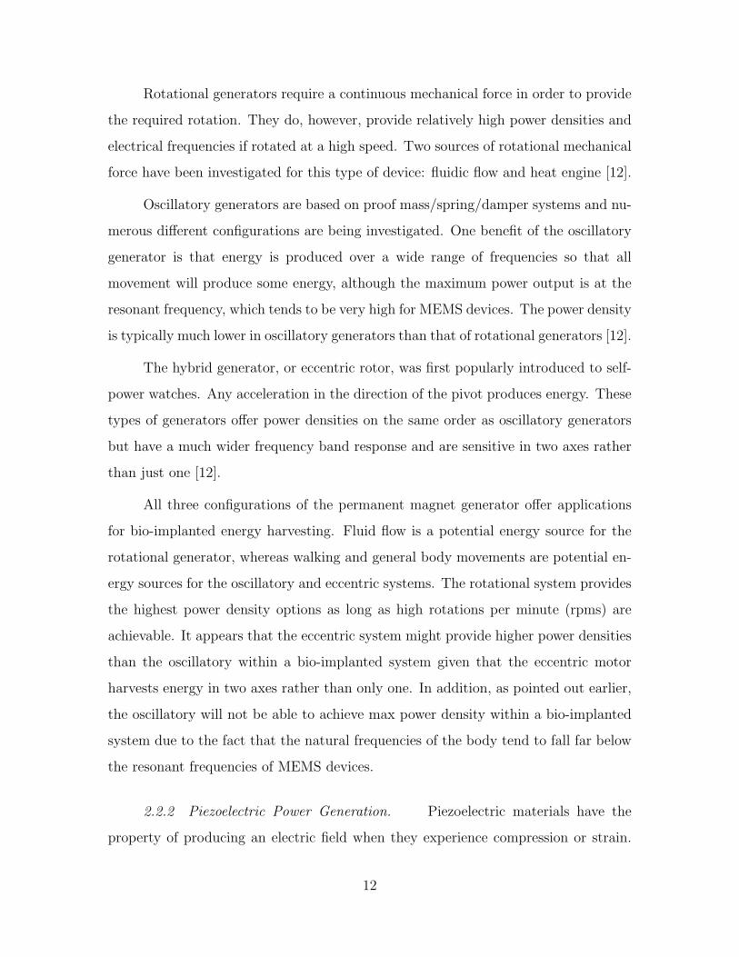
Rotational generators require a continuous mechanical force in order to provide
the required rotation. They do, however, provide relatively high power densities and
electrical frequencies if rotated at a high speed. Two sources of rotational mechanical
force have been investigated for this type of device: fluidic flow and heat engine [12].
Oscillatory generators are based on proof mass/spring/damper systems and nu-
merous different configurations are being investigated. One benefit of the oscillatory
generator is that energy is produced over a wide range of frequencies so that all
movement will produce some energy, although the maximum power output is at the
resonant frequency, which tends to be very high for MEMS devices. The power density
is typically much lower in oscillatory generators than that of rotational generators [12].
The hybrid generator, or eccentric rotor, was first popularly introduced to self-
power watches. Any acceleration in the direction of the pivot produces energy. These
types of generators offer power densities on the same order as oscillatory generators
but have a much wider frequency band response and are sensitive in two axes rather
than just one [12].
All three configurations of the permanent magnet generator offer applications
for bio-implanted energy harvesting. Fluid flow is a potential energy source for the
rotational generator, whereas walking and general body movements are potential en-
ergy sources for the oscillatory and eccentric systems. The rotational system provides
the highest power density options as long as high rotations per minute (rpms) are
achievable. It appears that the eccentric system might provide higher power densities
than the oscillatory within a bio-implanted system given that the eccentric motor
harvests energy in two axes rather than only one. In addition, as pointed out earlier,
the oscillatory will not be able to achieve max power density within a bio-implanted
system due to the fact that the natural frequencies of the body tend to fall far below
the resonant frequencies of MEMS devices.
2.2.2 Piezoelectric Power Generation. Piezoelectric materials have the
property of producing an electric field when they experience compression or strain.
12
The typical technique of harnessing this property to harvest energy consists of build-
ing piezoelectric structures that are sensitive to accelerations. As these accelerations
occur, the structures are simply compressed or stretched and thereby a current is
produced. However, just like the oscillatory permanent magnet method, resonant
frequencies are required in order to achieve the best results.
A proposed improvement on this technique makes use of an electromagnet to
vary the strain in the host material and thereby alter and expand the piezoelectric
material’s frequency domain. This method creates a broadband frequency spectrum
for the piezoelectric material, but requires the added complexity of another device to
vary the host’s strain [13].
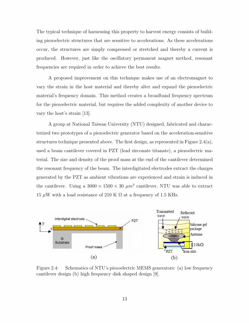
A group at National Taiwan University (NTU) designed, fabricated and charac-
terized two prototypes of a piezoelectric generator based on the acceleration-sensitive
structures technique presented above. The first design, as represented in Figure 2.4(a),
used a beam cantilever covered in PZT (lead zirconate titanate), a piezoelectric ma-
terial. The size and density of the proof mass at the end of the cantilever determined
the resonant frequency of the beam. The interdigitated electrodes extract the charges
generated by the PZT as ambient vibrations are experienced and strain is induced in
the cantilever. Using a 3000 × 1500 × 30 µm3 cantilever, NTU was able to extract
15 µW with a load resistance of 210 K Ω at a frequency of 1.5 KHz.
Figure 2.4: Schematics of NTU’s piezoelectric MEMS generators: (a) low frequencycantilever design (b) high frequency disk shaped design [9].
13
The second design, represented in Figure 2.4(b), functions at much higher fre-
quencies. The antenna is encased in a gel and sits on top of a PZT slab. Incoming high
frequency acoustic waves, approximately 75 KHz, vibrate the antenna and thereby
induce strain in the PZT slab underneath, resulting in charge being produced. Using
a spherical gel package, NTU was able to achieve a maximum power output of -40 dB
relative to the transmitted signal [9]. It must be noted that although this method
is not technically harvesting naturally occurring ambient energy, it does propose an
alternative solution to physically replacing batteries. One could potentially recharge
batteries or capacitors by sending a signal, wirelessly, to a bio-implanted system.
Given that these piezoelectric devices are so sensitive to accelerations, they
provide yet another option to harvest ambient energy for a bio-implanted device. The
power density appears to be on the same scale as what has been found with the
electromagnetic generator as well.
2.2.3 Electrostatic Power Generation. The last technique for power genera-
tion to be reviewed makes use of electrostatics at the micro scale. There are two types
of electrostatic power generation devices that will be examined here. One is termed as
a Coulomb Force Parametric Generator (CFPG) and the other is a Coulomb-Damped
Resonant Generator (CDRG). The CFPG generator produces power via accelerations
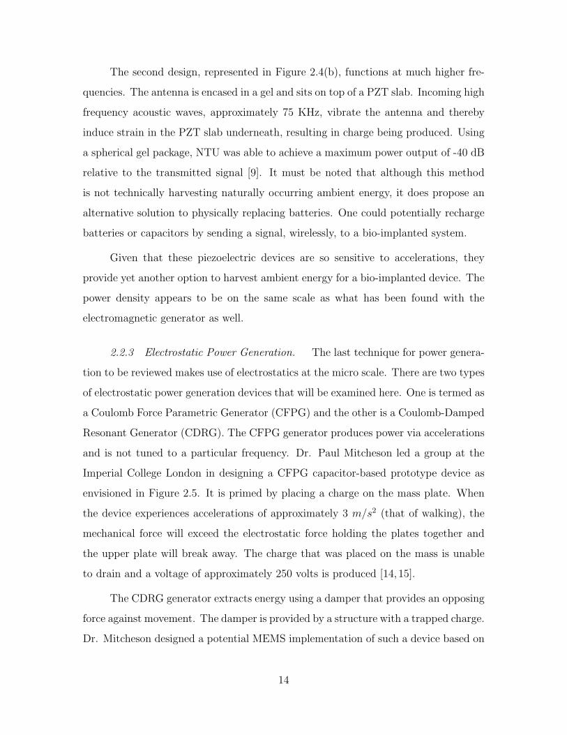
and is not tuned to a particular frequency. Dr. Paul Mitcheson led a group at the
Imperial College London in designing a CFPG capacitor-based prototype device as
envisioned in Figure 2.5. It is primed by placing a charge on the mass plate. When
the device experiences accelerations of approximately 3 m/s2 (that of walking), the
mechanical force will exceed the electrostatic force holding the plates together and
the upper plate will break away. The charge that was placed on the mass is unable
to drain and a voltage of approximately 250 volts is produced [14,15].
The CDRG generator extracts energy using a damper that provides an opposing
force against movement. The damper is provided by a structure with a trapped charge.
Dr. Mitcheson designed a potential MEMS implementation of such a device based on
14
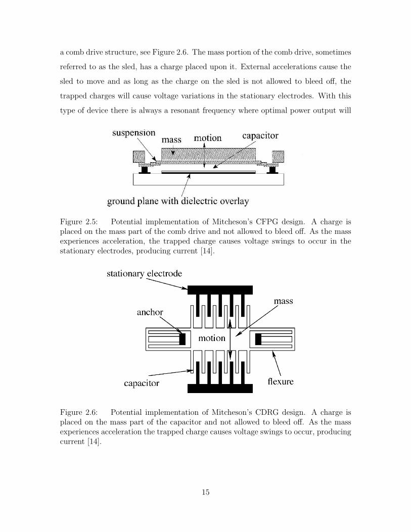
a comb drive structure, see Figure 2.6. The mass portion of the comb drive, sometimes
referred to as the sled, has a charge placed upon it. External accelerations cause the
sled to move and as long as the charge on the sled is not allowed to bleed off, the
trapped charges will cause voltage variations in the stationary electrodes. With this
type of device there is always a resonant frequency where optimal power output will
Figure 2.5: Potential implementation of Mitcheson’s CFPG design. A charge isplaced on the mass part of the comb drive and not allowed to bleed off. As the massexperiences acceleration, the trapped charge causes voltage swings to occur in thestationary electrodes, producing current [14].
Figure 2.6: Potential implementation of Mitcheson’s CDRG design. A charge isplaced on the mass part of the capacitor and not allowed to bleed off. As the massexperiences acceleration the trapped charge causes voltage swings to occur, producingcurrent [14].
15
occur. With MEMS devices of this type, the resonant frequency tends to be in the
tens of KHz range [14], a range difficult to obtain in the human body.
Both electrostatic generator methods discussed here, CFPG and CDRG, are po-
tential candidates for bio-implanted devices. However, the high resonant frequencies
required for power generation using the CDRG method might result in extremely low
power output.
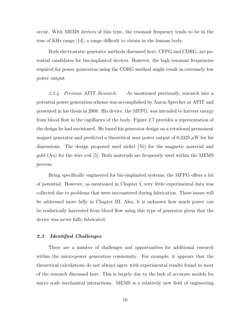
2.2.4 Previous AFIT Research. As mentioned previously, research into a
potential power generation scheme was accomplished by Aaron Sprecher at AFIT and
presented in his thesis in 2008. His device, the MFPG, was intended to harvest energy
from blood flow in the capillaries of the body. Figure 2.7 provides a representation of
the design he had envisioned. He based his generator design on a rotational permanent
magnet generator and predicted a theoretical max power output of 0.3325 µW for his
dimensions. The design proposed used nickel (Ni) for the magnetic material and
gold (Au) for the wire coil [5]. Both materials are frequently used within the MEMS
process.
Being specifically engineered for bio-implanted systems, the MFPG offers a lot
of potential. However, as mentioned in Chapter I, very little experimental data was
collected due to problems that were encountered during fabrication. These issues will
be addressed more fully in Chapter III. Also, it is unknown how much power can
be realistically harvested from blood flow using this type of generator given that the
device was never fully fabricated.
2.3 Identified Challenges
There are a number of challenges and opportunities for additional research
within the micro-power generation community. For example, it appears that the
theoretical calculations do not always agree with experimental results found in most
of the research discussed here. This is largely due to the lack of accurate models for
micro scale mechanical interactions. MEMS is a relatively new field of engineering
16
(a) MFPG Top View
(b) MFPG Side View
Figure 2.7: The MFPG was designed to harvest energy from blood flow. The deviceis assembled by stacking three wafers. (a) A top view illustrates the channels whereblood would flow and the turbine used to harvest the energy. (b) The side viewillustrates how the turbine is connected to the rotor magnets with a shaft. As theturbine and rotor magnets rotate, a current is induced in the gold wire coil below themagnets [5].
17
and there is still much to learn. Of particular interest is how permanent magnets
scale at the micro level. Severe discrepancies have been noted between predicted val-
ues and experimental results [12]. Actually fabricating the devices discussed here and
characterizing them would provide much data to potentially develop more accurate
models for this area of research.
In addition, electromagnetic generators require low-friction. Given that only
a small amount of ambient energy will be collected in a micro generator system, it
is essential that each system be extremely efficient so as to maximize power output.
Potential solutions include micro ball bearings, gas bearings, and magnetic bearings,
all of which are currently being researched. However, even if one of these technologies
was found superior, the integration of such a technology only leads to more complexity
in the fabrication process [12].
Another challenge includes the fact that industry’s capability to deposit and
pattern certain ferromagnetic materials at the micro level has yet to approach their
capability at the macro level. For electromagnetic generators, the use of high energy
density magnetic materials such as CoPt, FePt, SmCo or NdFeB is essential, but
microfabrication methods such as sputtering and evaporation are relatively primitive
for these types of materials. In addition, to achieve optimal magnetic properties, high
temperature anneals are required. The annealing process allows for more of the mag-
netic moments to align, creating stronger fields, but the high temperature also limits
the types of materials that can be integrated with the magnets [12]. Piezoelectric
materials are just as difficult to pattern and deposit at the micro scale. Numerous
processes are currently being used, such as sol-gel deposition and ”jet-printing,” but
a standardized, high resolution process is not currently available [9].
Along with discovering new harvesting techniques, engineers must also design
new micro-power devices and circuits that convert and condition the supplied energy
so as to properly power the IC portion of the integrated system. This has proven
difficult due to the fact that some ambient energy harvesting techniques do not provide
18
continuous energy supplies, are not necessarily harmonic and often provide only short
pulses of energy. The group at the Imperial College London claim to have designed
a converter device for their electrostatic generator that takes all of these limitations
into consideration by analyzing the system parasitics and selecting specific transistor
devices that optimized their converter [15]. This converter, however, is applicable to
only a CFPG type of electrostatic generator. Similar research needs to be applied to
all the other types of generators discussed in this paper as well.
This thesis effort will focus on collecting more data applicable to two of these
micro-power generation issues–matching experimental with theoretical data and pat-
terning magnetic material at the MEMS level. A test apparatus will be designed and
experimental power generation data will be collected. This experimental data can
then be compared with the theoretical calculations and used to improve the models.
In addition, it is anticipated that throughout the process of fabricating the magnets
to be used in the micro-generator, a successful patterning process will be identified.
2.4 Chapter Summary
This chapter has reviewed multiple methods of micro power generation being
researched today. Electromagnetic, piezoelectric and electrostatic generators appear
to be the most logical solutions for bio-implanted devices. The benefits and difficul-
ties associated with each type were discussed. In addition multiple challenges and
potential research topics for this area of study were laid out.
Without a doubt there is much to learn and discover about micro power gener-
ation and the capability to harness the ambient energy that surrounds us every day.
It is the intent of this thesis research to obtain more data for the community at large
in order to increase the knowledge base for this area of interest.
19
III. Methodology and Theory
As discussed in previous chapters, this research is based on the MFPG design pre-
sented by a previous student at AFIT, Aaron Sprecher [5]. The MFPG design pro-
posed harvesting energy from blood flow in the human body. Blood flow actuated
micro turbines which, in turn, rotated magnetic rotors above stator coils, thereby
inducing a current in the coils. Given that the device was never fully fabricated or
tested, this thesis will build upon the original generator design and characterize the
potential power output of the proposed design.
The process of designing and fabricating a micro-electromagnetic generator re-
quires knowledge of multiple engineering disciplines including: electromagnetism,
microfabrication techniques, and microelectronic device physics. This chapter will
present the methodology utilized in this research effort alongside the associated the-
ory and design approaches. Primarily, it is essential to understand how electromag-
netic generators function. By investigating how they work, one can identify what
parameters optimize performance, and design to those optimizations.
3.1 Electromagnetic Generators
Electromagnetic generators form the basis for the majority of today’s energy
production. Coal, nuclear, wind, and hydroelectric power generation all make use
of electromagnetic generators. All of these generators consist of a turbine, rotor
and stator. The rotor and stator make up what will be referred to as the active
generator, meaning that they contain the magnetic and conductive coil components
of the generator, and therefore are the primary source of power generation within the
device.
The turbine makes direct contact with a fluid flow, such as steam, wind, water,
etc., and is shaped such that the interaction with the fluid flow causes the turbine to
rotate. The rotor is attached to the turbine via a shaft and is the moving portion of
the active generator. It consists of either an array of magnets or an array of conductive
coils. The stator is stationary and is composed of coils if the rotor is magnetic and of
20
magnets if the rotor is an array of coils. As the fluid flow pushes through the turbine,
it rotates the turbines, and therefore the rotor as well. This rotation induces a current
in the coils and power is transduced from the kinetic energy of fluid flow to electric
energy.
3.1.1 Theory of Electromagnetic Generators. Electromagnetic generators
function on the principle of electromagnetic induction, also known as Faraday’s Law.
Faraday’s Law states that when a magnet and a coil are relatively close, any time
changing magnetic flux results in a current flow in the coil. Quantitatively, Faraday’s
Law is expressed as
ξ = −NdΦB
dt(3.1)
where ξ is the electromotive force (emf) for voltage, N is the number of turns of the
coil and dΦB/dt is the rate of change of magnetic flux with time [16]. Figure 3.1
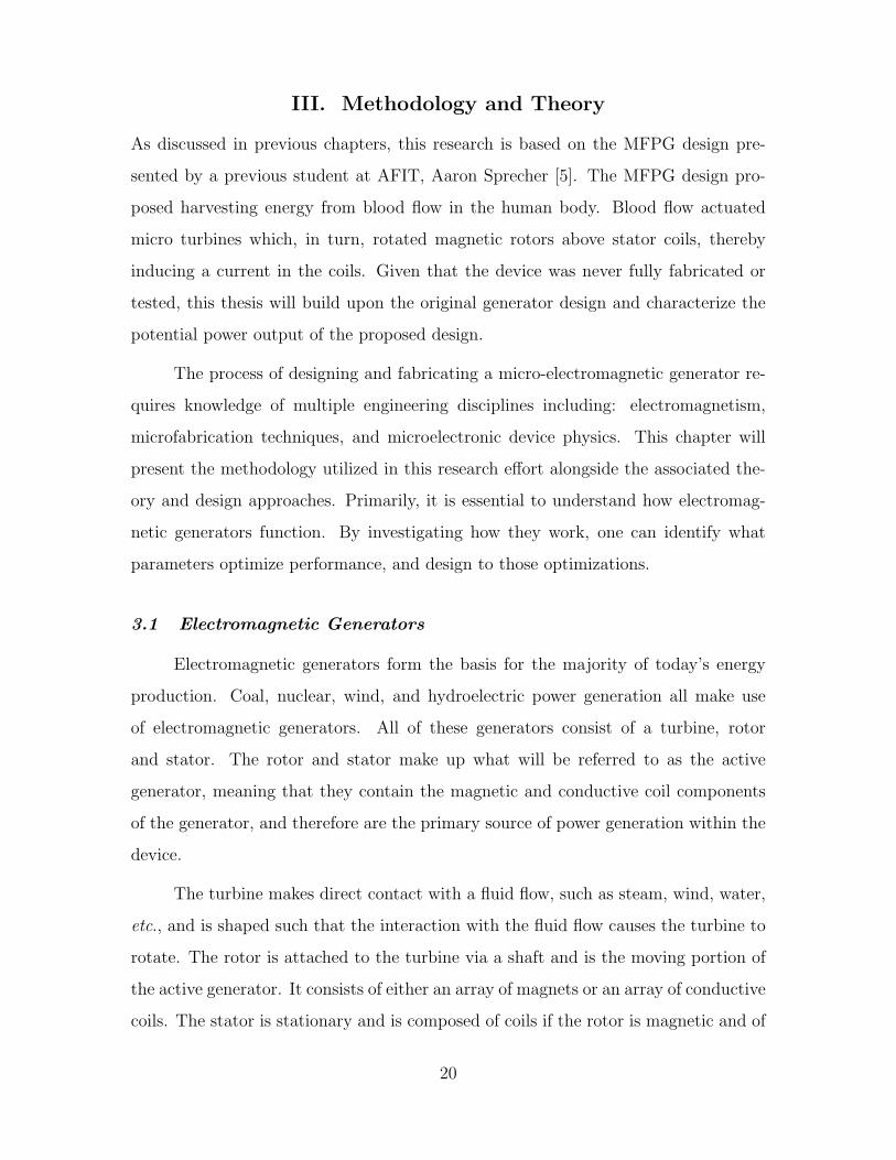
provides an illustration of this law. As the bar magnet is moved within the coil, a
current is induced in the coil and the galvanometer, or ammeter, is deflected. The
Figure 3.1: As the bar magnet is moved in and out of the coil, the galvanometerregisters current flow. However, the current only flows during motion of the magnetor coil. No current flows when the coil and magnet are at rest [17].
21
galvanometer is deflected in the opposite direction as the magnet is withdrawn from
the coil.
In addition, Maxwell’s 4th equation, known as the Ampere-Maxwell Law, states
that
∇×B = µ0J + µ0ε0∂E/∂t. (3.2)
This law defines the relationship of the curl of the magnetic field (∇×B) to the current
density (J) and displacement current (∂E/∂t). µ0 is the permeability of free space
and ε0 is the permittivity of free space. It is through the use of Ampere-Maxwell’s
Law that one can also determine the direction of the current flow induced by using
the right-hand rule. The right-hand rule, as it pertains to magnetic fields, states that
if one curls their right hand in the direction of the B field then the direction that
your thumb is pointing is also the direction of current flow.
Therefore, using Equation 3.1 and Equation 3.2 it is shown that a time changing
magnetic field will induce a current within a wire in that field and the current is
optimized when the current flow, the magnetic field and the direction of motion are
all mutually orthogonal. These laws form the basis for the development of a micro-
generator.
3.1.2 Generator Design Parameters. The driving factor for designing the
micro-generator is to maximize power output for the device. Equation 3.1 states that
the number of turns in the coil and the rate of change of the magnetic field directly
affect the amount of power output. Equation 3.2 states that the magnitude of the
B field and orientation of the B field to the coil will affect the current density and
electric field induced as well. It can also be inferred that the closer the magnet is to
the coil then the stronger the coil will be affected by the magnetic field. The amount
of power that is consumed in the coil of the generator will have a direct affect on
the amount of power delivered to the load as well. This consumption of power can
be reduced by decreasing the resistance of the coil. All of these considerations are
compiled in Table 3.1 for quick reference.
22
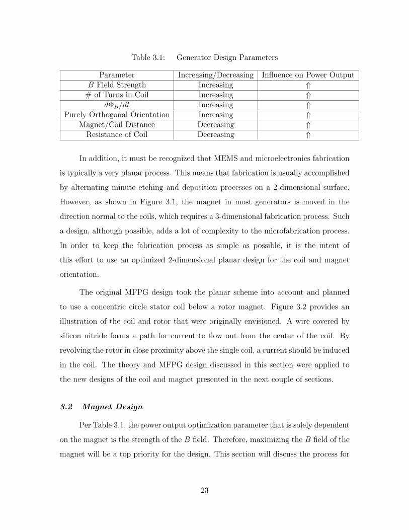
Table 3.1: Generator Design Parameters
Parameter Increasing/Decreasing Influence on Power OutputB Field Strength Increasing ⇑# of Turns in Coil Increasing ⇑
dΦB/dt Increasing ⇑Purely Orthogonal Orientation Increasing ⇑
Magnet/Coil Distance Decreasing ⇑Resistance of Coil Decreasing ⇑
In addition, it must be recognized that MEMS and microelectronics fabrication
is typically a very planar process. This means that fabrication is usually accomplished
by alternating minute etching and deposition processes on a 2-dimensional surface.
However, as shown in Figure 3.1, the magnet in most generators is moved in the
direction normal to the coils, which requires a 3-dimensional fabrication process. Such
a design, although possible, adds a lot of complexity to the microfabrication process.
In order to keep the fabrication process as simple as possible, it is the intent of
this effort to use an optimized 2-dimensional planar design for the coil and magnet
orientation.
The original MFPG design took the planar scheme into account and planned
to use a concentric circle stator coil below a rotor magnet. Figure 3.2 provides an
illustration of the coil and rotor that were originally envisioned. A wire covered by
silicon nitride forms a path for current to flow out from the center of the coil. By
revolving the rotor in close proximity above the single coil, a current should be induced
in the coil. The theory and MFPG design discussed in this section were applied to
the new designs of the coil and magnet presented in the next couple of sections.
3.2 Magnet Design
Per Table 3.1, the power output optimization parameter that is solely dependent
on the magnet is the strength of the B field. Therefore, maximizing the B field of the
magnet will be a top priority for the design. This section will discuss the process for
23
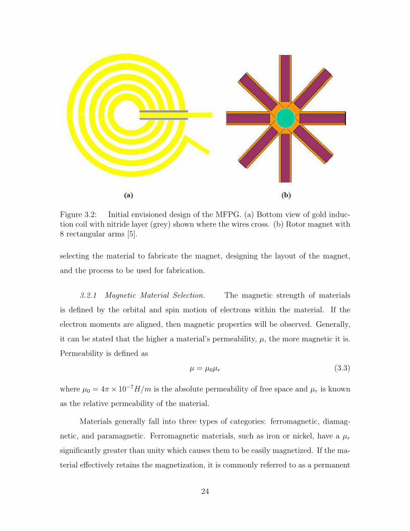
Figure 3.2: Initial envisioned design of the MFPG. (a) Bottom view of gold induc-tion coil with nitride layer (grey) shown where the wires cross. (b) Rotor magnet with8 rectangular arms [5].
selecting the material to fabricate the magnet, designing the layout of the magnet,
and the process to be used for fabrication.
3.2.1 Magnetic Material Selection. The magnetic strength of materials
is defined by the orbital and spin motion of electrons within the material. If the
electron moments are aligned, then magnetic properties will be observed. Generally,
it can be stated that the higher a material’s permeability, µ, the more magnetic it is.
Permeability is defined as
µ = µ0µr (3.3)
where µ0 = 4π× 10−7H/m is the absolute permeability of free space and µr is known
as the relative permeability of the material.
Materials generally fall into three types of categories: ferromagnetic, diamag-
netic, and paramagnetic. Ferromagnetic materials, such as iron or nickel, have a µr
significantly greater than unity which causes them to be easily magnetized. If the ma-
terial effectively retains the magnetization, it is commonly referred to as a permanent
24
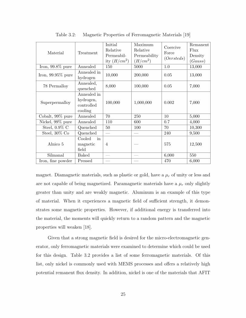
Table 3.2: Magnetic Properties of Ferromagnetic Materials [19]
Material Treatment
InitialRelativePermeabil-ity (H/cm2)
MaximumRelativePermeability(H/cm2)
CoerciveForce(Oersteds)
RemanentFluxDensity(Gauss)
Iron, 99.8% pure Annealed 150 5000 1.0 13,000
Iron, 99.95% pureAnnealed inhydrogen
10,000 200,000 0.05 13,000
78 PermalloyAnnealed,quenched
8,000 100,000 0.05 7,000
Superpermalloy
Annealed inhydrogen,controlledcooling
100,000 1,000,000 0.002 7,000
Cobalt, 99% pure Annealed 70 250 10 5,000Nickel, 99% pure Annealed 110 600 0.7 4,000
Steel, 0.9% C Quenched 50 100 70 10,300Steel, 30% Co Quenched — — 240 9,500
Alnico 5Cooled inmagneticfield
4 — 575 12,500
Silmanal Baked — — 6,000 550Iron, fine powder Pressed — — 470 6,000
magnet. Diamagnetic materials, such as plastic or gold, have a µr of unity or less and
are not capable of being magnetized. Paramagnetic materials have a µr only slightly
greater than unity and are weakly magnetic. Aluminum is an example of this type
of material. When it experiences a magnetic field of sufficient strength, it demon-
strates some magnetic properties. However, if additional energy is transferred into
the material, the moments will quickly return to a random pattern and the magnetic
properties will weaken [18].
Given that a strong magnetic field is desired for the micro-electromagnetic gen-
erator, only ferromagnetic materials were examined to determine which could be used
for this design. Table 3.2 provides a list of some ferromagnetic materials. Of this
list, only nickel is commonly used with MEMS processes and offers a relatively high
potential remanent flux density. In addition, nickel is one of the materials that AFIT
25
has the ability to deposit. An 80%/20% nickel/iron alloy has been electroplated in
MEMS processes as well and offers a higher permeability [20], however, AFIT does
not have this material readily available for deposition. A pure nickel deposition will
be used for this effort.
3.2.2 Magnet Layout Design. It is not completely clear how the layout of
the magnets will affect the power output of the device. As discussed earlier, most
electromagnetic generators operate in a 3-dimensional environment, whereas, the mi-
cro design is intended to be a planar scheme. No relevant research was found that
addressed how to best layout the magnetic portion of the generator with such a planar
design. There are, however, two aspects of the layout that are important and did play
into the proposed designs.
First, it was decided that the magnets should be attached to the rotor and the
coil should be the stator portion of the generator, just as was originally envisioned
with the MFPG. The reasoning is that the coils will be attached to a load. Keeping
the load and coil stationary would reduce design complexity significantly. The mag-
nets, however, do not require any physical interface with another component and are
therefore the best choice for the rotor.
In addition, it is known that a time-varying change in magnetic field will be
required to induce the current per Faraday’s Law. For a planar design, such as that
proposed with the MFPG, this translates into a gap between magnets. The gap allows
for the coils to experience variations in the magnetic fields. When a magnet is directly
over the coils, a strong magnetic field will be experienced. As the magnet moves off
of the coil, the field is decreased. The rate of change of the field will be defined by
the speed of rotation of the turbines.
In order to identify some trends and determine if the magnet layout really makes
an appreciable difference in power output, a few different layouts were evaluated. All
layouts were created using the Layout Editor (L-Edit) of MEMS ProTM Version 6.0.
The rotor layouts are of two different varieties: rectangular arms and segmented
26
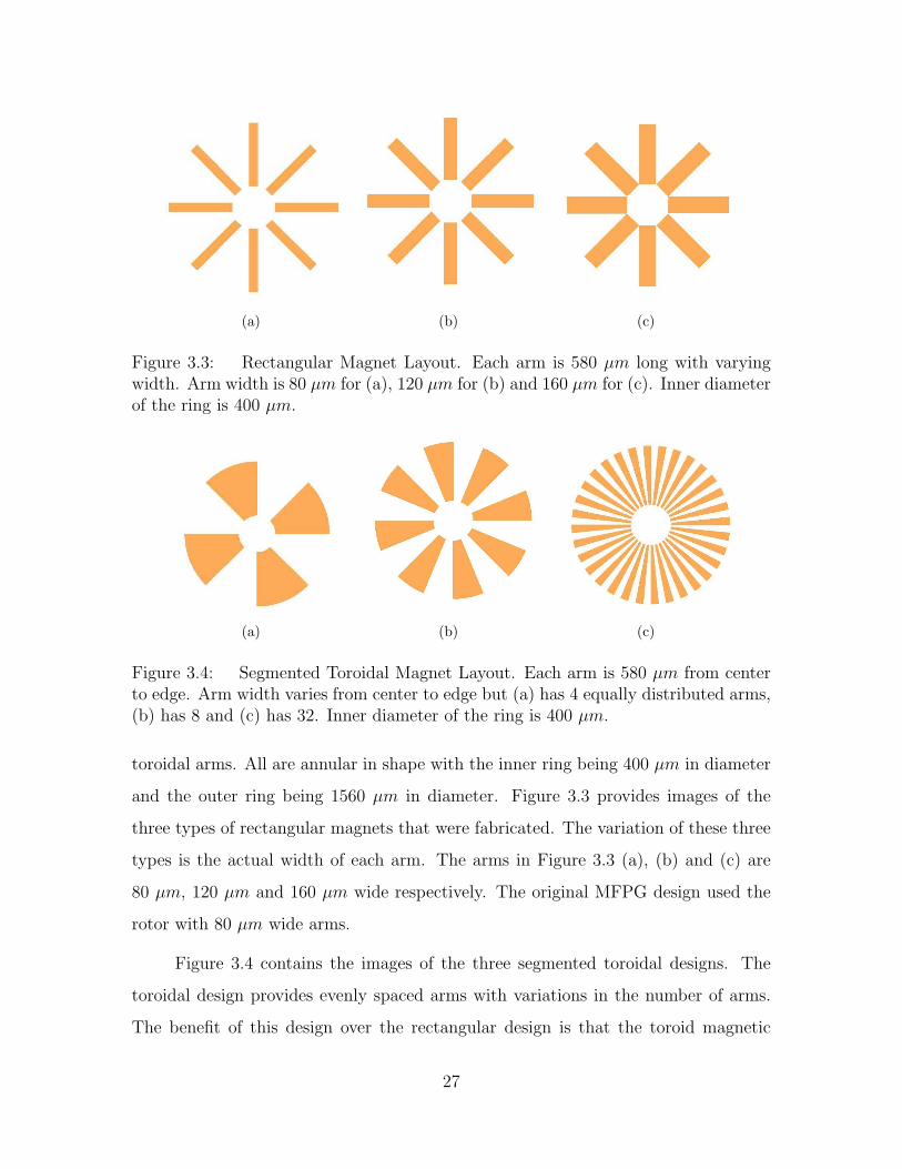
(a) (b) (c)
Figure 3.3: Rectangular Magnet Layout. Each arm is 580 µm long with varyingwidth. Arm width is 80 µm for (a), 120 µm for (b) and 160 µm for (c). Inner diameterof the ring is 400 µm.
(a) (b) (c)
Figure 3.4: Segmented Toroidal Magnet Layout. Each arm is 580 µm from centerto edge. Arm width varies from center to edge but (a) has 4 equally distributed arms,(b) has 8 and (c) has 32. Inner diameter of the ring is 400 µm.
toroidal arms. All are annular in shape with the inner ring being 400 µm in diameter
and the outer ring being 1560 µm in diameter. Figure 3.3 provides images of the
three types of rectangular magnets that were fabricated. The variation of these three
types is the actual width of each arm. The arms in Figure 3.3 (a), (b) and (c) are
80 µm, 120 µm and 160 µm wide respectively. The original MFPG design used the
rotor with 80 µm wide arms.
Figure 3.4 contains the images of the three segmented toroidal designs. The
toroidal design provides evenly spaced arms with variations in the number of arms.
The benefit of this design over the rectangular design is that the toroid magnetic
27
fields should be much more evenly distributed from the center of the coils to the edge
of the coils than the fields produced by the rectangular arms. Experimentation will
determine if this favorably affects power output or not.
3.2.3 Nickel Deposition Process. The actual deposition of the nickel will
play a very important role as well. As discussed earlier, magnetism is a result of the
vector sum of multiple electron spins. Therefore, the more massive the nickel deposit,
the stronger the magnetic field because more nickel atoms are contributing to the
vector sum. However, a balance must be found given that the final generator should
be micro-sized. In addition, to maximize the remanent flux density of the nickel, the
deposition needs to be as uniform and deformity-free as possible.
Nickel is typically deposited by sputtering, evaporation, or electroplating within
the microfabrication community. Electroplating is the conventional MEMS process
for depositing relatively large amounts of nickel of more than 1 to 2 µm. It allows one
to deposit large amounts of metal onto a MEMS structure in a reliable and measurable
way.
The nickel electroplating process at local facilities has not been fully character-
ized. Due to that fact, a significant portion of this research will investigate the plating
process in an attempt to characterize it so that deposited nickel for the rotor magnets
will be as pure and clean of defects as possible with the provided tools. The typical
process of electroplating is represented by Figure 3.5. Passing a current between two
electrodes that are immersed in a conductive solution of nickel ions causes the anode,
usually a nickel plate or bar, to dissolve. The cathode, however, attracts the ions in
the solution. As the ions touch the cathode, the cathode neutralizes the charge of
the ion and a nickel atom is deposited on the cathode [21]. A reverse current is also
possible and would cause the exact opposite to occur, the cathode would give off ions
and the anode would have nickel deposited on it.
There are numerous parameters that play a significant role in the results of the
electroplating process. They include:
28
Figure 3.5: Process of Electroplating Nickel. An applied current flow causes nickelions to be removed from the anode and deposited on the cathode. [5].
• Wafer Preparation: The best results will be achieved by using a fresh, clean
wafer. One must avoid having any oxidation or other foreign material on the
surface of the wafer prior to being placed in the electroplating bath. If a foreign
material is on the substrate prior to the plating process, then the new material
will not be able to adhere as well as if there was a clean surface to be plated to.
• Seed Layer: The seed layer is of the utmost importance. It provides an interface
between the wafer material and the metal to be electroplated. Electroplating
would not occur without a seed layer and certain metals provide better seeds for
nickel than others. The best seed layers for nickel plating will be investigated
later in this research.
• Bath Composition and State: There are numerous solutions of nickel baths
available for purchase. Some provide lower stress while others offer a more shiny
29
surface. In addition, as the bath is used over time the composition is changed
and the pH is changed, which will alter results over time. The temperature of
the bath during the process is another critical parameter that must be adjusted
to obtain desired results. One must also consider that when the bath is stored at
high or low temperatures, this could potentially lead to the solution becoming
hydrolyzed. Hydrolysis is the decomposition of the original solution molecules,
and for some plating baths, the hydrolyzed solution is less soluble and tends to
lead to increased tensile stress [21].
• Forward and Reverse Current Density: The current density determines how
rapidly the plating process will occur. A reverse density is typically used in
order to produce an even distribution across the surface being plated. The
edges of the sample usually experience a much higher current than the center
and, therefore, are plated more rapidly. A reverse current causes some of that
excess to be released. A correct balance of the two should produce a uniform
distribution across the surface.
• Duty Cycle: Not only must one consider the amount of forward and reverse
current to use, but the amount of time that each direction is applied should
be considered as well. The duty cycle is usually expressed as a ratio such as
“60/40”. This denotes that 60% of the duty cycle is made up by the forward
current and the 40% is made up of the reverse current.
• Time: The total amount of time the sample is in the bath with the current
being applied determines the thickness of the plating. It can be expressed in
two forms: minutes or amp-minutes. Minutes is the amount of time that the
sample is actually in the bath. Amp-minutes denotes the number of minutes
that a full amp of current is being applied to the sample. This is usually the
number that is input into the electroplating power supply. The relationship is
therefore stated: amp-minutes is equal to the average forward current multiplied
by plating time.
30
• Position of Anode: The proximity of the anode to the sample makes a significant
difference in the plating process, for if the anode is placed closer to the sample
cathode, then the plating process will be accelerated. Therefore, the forward
and reverse current and the amount of time in the bath will have to be altered
in order to account for this.
As one can see, many parameters will affect the process for depositing the mag-
netic material. Chapter IV will discuss the fabrication process used for the microgen-
erator and Chapter V will present the results observed from depositing the nickel.
3.2.4 Magnetization of Nickel Deposit. In determining the proper method
for magnetizing, or polarizing, the rotor arms one must consider the orientation to be
used with the rotor magnets and stator coil. As discussed earlier in this chapter, in
order to maximize current density, one must ensure that the direction of field variation,
direction of the B fields, and the flow of current are all mutually orthogonal. Figure 3.6
provides a representation of an orientation that provides such orthogonality. This
figure contains one of the varieties of magnetic rotors (grey) and stator coils (gold) to
be fabricated. The arrows provide an illustration of the magnetic field lines produced
when the magnets are polarized top to bottom as shown. When rotated, the field
lines will be perpendicular to the direction of rotation as well as to the direction of
current flow in the coils, satisfying the requirements for optimal current density.
Given that nickel is a ferromagnetic material, significant polarization can be
accomplished by placing the deposited nickel in a strong external magnetic field. This
external magnetic field aligns the electron spins within the nickel, thereby magnetizing
the nickel. By adding heat to the process, the alignment occurs more quickly. The
extra energy allows more atoms to align properly faster. As long as the nickel does
not experience excessive heat or kinetic energy, then it will remain polarized.
Optimally this polar alignment would be accomplished in situ as the nickel is
deposited. However, available resources do not allow for this. For this reason a Hall
Measurement System manufactured by LakeShore will be used to polarize the nickel
31
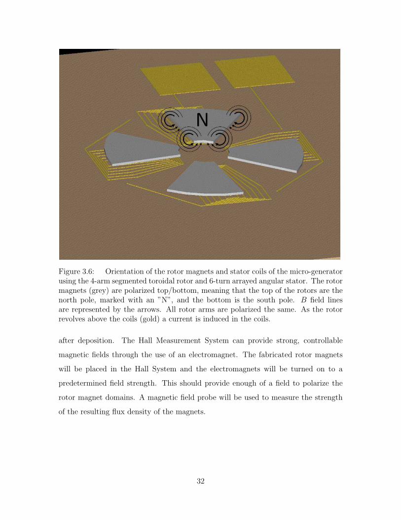
Figure 3.6: Orientation of the rotor magnets and stator coils of the micro-generatorusing the 4-arm segmented toroidal rotor and 6-turn arrayed angular stator. The rotormagnets (grey) are polarized top/bottom, meaning that the top of the rotors are thenorth pole, marked with an ”N”, and the bottom is the south pole. B field linesare represented by the arrows. All rotor arms are polarized the same. As the rotorrevolves above the coils (gold) a current is induced in the coils.
after deposition. The Hall Measurement System can provide strong, controllable
magnetic fields through the use of an electromagnet. The fabricated rotor magnets
will be placed in the Hall System and the electromagnets will be turned on to a
predetermined field strength. This should provide enough of a field to polarize the
rotor magnet domains. A magnetic field probe will be used to measure the strength
of the resulting flux density of the magnets.
32
Table 3.3: Resistivity of Common MEMS Compatible Metals at 20 C [22,23]Material Resistivity ρ (Ω−m)Copper 1.678× 10⁻⁸
Gold 2.214× 10⁻⁸
Aluminum 2.65× 10⁻⁸
Tungsten 5.28× 10⁻⁸
Zinc 5.9× 10⁻⁸
Nickel 6.93× 10⁻⁸
Chromium 12.5× 10⁻⁸
Titanium 42× 10−8
3.3 Coil Design
Referring back to Table 3.1, we can see that two parameters are purely depen-
dent on the coil design: resistance of the coil and the number of turns in the coil. In
addition, one must ensure that the orientation of the coil to the magnet induces the
desired current. All of these parameters will be discussed in this section as well as
the resulting coil designs for this effort.
3.3.1 Coil Material Selection. Resistance is a measure of how easily a
current can flow in a material. Analytically it is defined by the equation
R =ρL
A(3.4)
where R is resistance, ρ is the resistivity of a material, L is the length of the path the
current is flowing through and A is the cross sectional area of that path. Resistivity
is a material constant and, by Equation 3.4, is directly proportional to resistance.
Table 3.3 provides a list of some metals commonly used with microelectronics and
their respective resistivity values. Copper has the lowest resistivity, but oxidizes
quickly when exposed to air. Oxidation causes difficulty in making good metal-to-
metal connections when multiple depositions are used. Gold was selected as the
material for the coils because it has the second lowest resistivity and does not oxidize.
Low resistivity leads to low resistance and, thereby, less power loss in the coils.
33
3.3.2 Coil Layout. In designing the layout of the coils, numerous aspects
need to be taken into consideration to optimize the power output of the micro-
generator. These include the following:
• Cross-Sectional Area and Length of Wires in the Coil
• Design Current Path from Center of Coil Without Shorting the Circuit
• Orthogonality of Current Flow to B Field and Flux
3.3.2.1 Cross-Sectional Area and Length of Wires in the Coil. Equa-
tion 3.4 defines resistance as inversely proportional to the cross-sectional area of the
wires and directly proportional to the length of the wire. Given that information, the
coil layout should be as short in length as possible with a cross-sectional area as large
as possible in order to lower resistance and thereby maximize power output.
Cross-sectional area is easily varied by increasing the amount of gold that is
deposited for each coil, thereby changing the thickness of the coil. Width of the coil
could also be varied to increase cross-sectional area. It was decided to keep width
constant among all the coils to assist in standardizing the testing of the generator
power output. All coils presented in this thesis have a wire width of 10 µm.
Regarding the length of the wire coils, there is a tradeoff that needs to be
managed. As discussed at the beginning of this chapter, one of the parameters that
plays into the efficiency of the overall generator is the number of turns in the coil.
However, as you increase the number of turns, you also increase the length of the
current path and therefore the resistance and power lost in the coil, as illustrated
with the plot in Figure 3.7. It must also be remembered that this is to be a micro-
generator. Increasing the number of turns translates into significant increases in size
of the layout footprint due to the planar nature of the design. For example, a 12-turn
angled coil requires 51% more device surface area than the 6-turn angled coil. For
this effort, coils with 14, 12, and 6 turns were designed and fabricated.
34
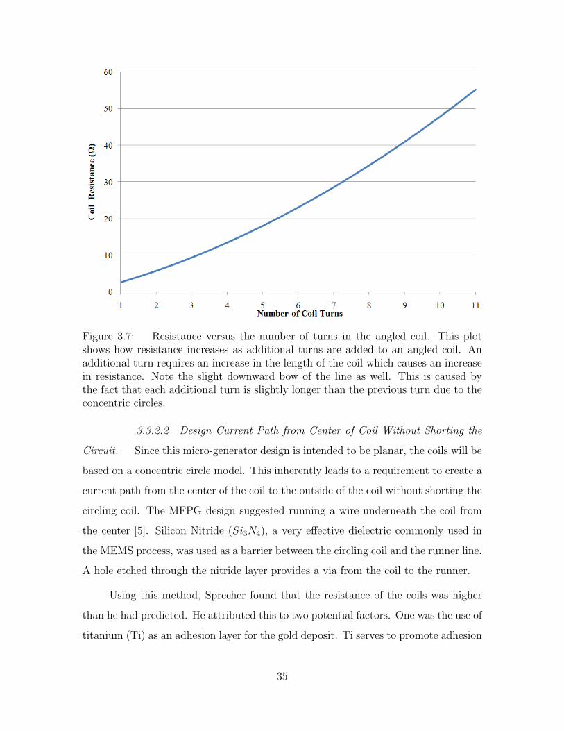
Figure 3.7: Resistance versus the number of turns in the angled coil. This plotshows how resistance increases as additional turns are added to an angled coil. Anadditional turn requires an increase in the length of the coil which causes an increasein resistance. Note the slight downward bow of the line as well. This is caused bythe fact that each additional turn is slightly longer than the previous turn due to theconcentric circles.
3.3.2.2 Design Current Path from Center of Coil Without Shorting the
Circuit. Since this micro-generator design is intended to be planar, the coils will be
based on a concentric circle model. This inherently leads to a requirement to create a
current path from the center of the coil to the outside of the coil without shorting the
circling coil. The MFPG design suggested running a wire underneath the coil from
the center [5]. Silicon Nitride (Si3N4), a very effective dielectric commonly used in
the MEMS process, was used as a barrier between the circling coil and the runner line.
A hole etched through the nitride layer provides a via from the coil to the runner.
Using this method, Sprecher found that the resistance of the coils was higher
than he had predicted. He attributed this to two potential factors. One was the use of
titanium (Ti) as an adhesion layer for the gold deposit. Ti serves to promote adhesion
35
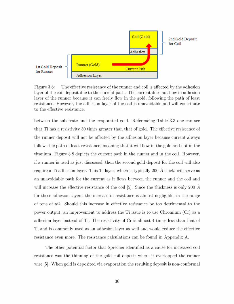
Figure 3.8: The effective resistance of the runner and coil is affected by the adhesionlayer of the coil deposit due to the current path. The current does not flow in adhesionlayer of the runner because it can freely flow in the gold, following the path of leastresistance. However, the adhesion layer of the coil is unavoidable and will contributeto the effective resistance.
between the substrate and the evaporated gold. Referencing Table 3.3 one can see
that Ti has a resistivity 30 times greater than that of gold. The effective resistance of
the runner deposit will not be affected by the adhesion layer because current always
follows the path of least resistance, meaning that it will flow in the gold and not in the
titanium. Figure 3.8 depicts the current path in the runner and in the coil. However,
if a runner is used as just discussed, then the second gold deposit for the coil will also
require a Ti adhesion layer. This Ti layer, which is typically 200 A thick, will serve as
an unavoidable path for the current as it flows between the runner and the coil and
will increase the effective resistance of the coil [5]. Since the thickness is only 200 A
for these adhesion layers, the increase in resistance is almost negligible, in the range
of tens of µΩ. Should this increase in effective resistance be too detrimental to the
power output, an improvement to address the Ti issue is to use Chromium (Cr) as a
adhesion layer instead of Ti. The resistivity of Cr is almost 4 times less than that of
Ti and is commonly used as an adhesion layer as well and would reduce the effective
resistance even more. The resistance calculations can be found in Appendix A.
The other potential factor that Sprecher identified as a cause for increased coil
resistance was the thinning of the gold coil deposit where it overlapped the runner
wire [5]. When gold is deposited via evaporation the resulting deposit is non-conformal
36
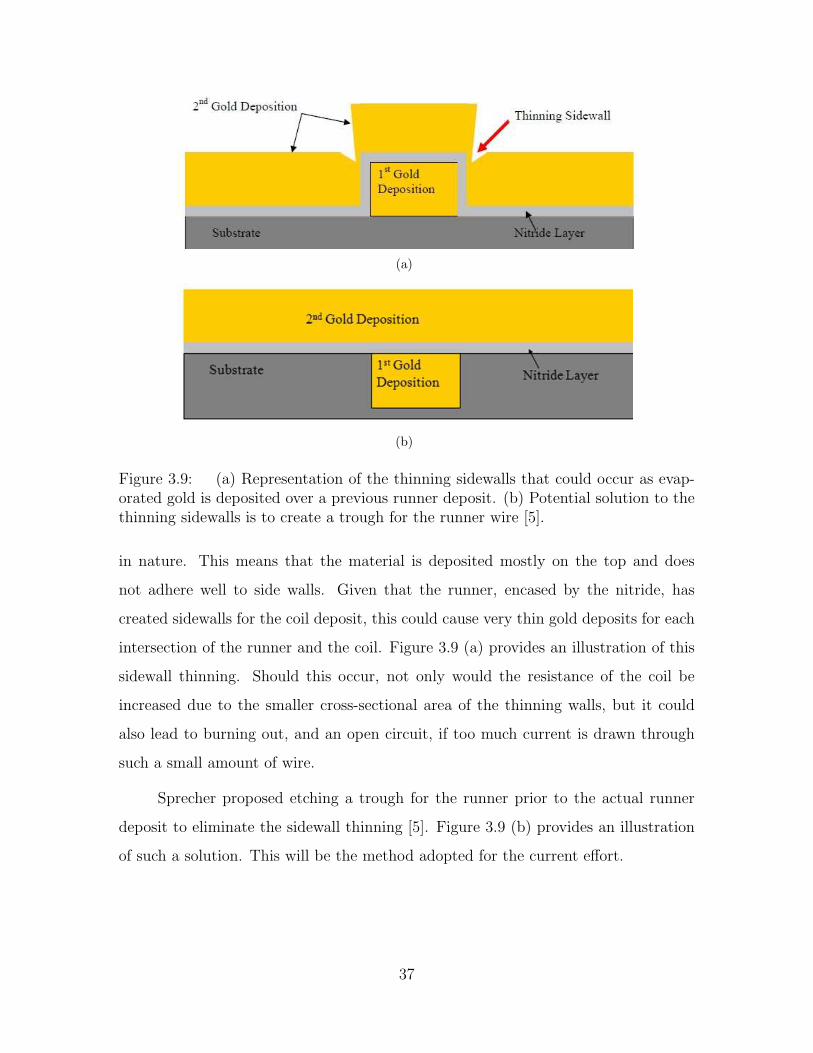
(a)
(b)
Figure 3.9: (a) Representation of the thinning sidewalls that could occur as evap-orated gold is deposited over a previous runner deposit. (b) Potential solution to thethinning sidewalls is to create a trough for the runner wire [5].
in nature. This means that the material is deposited mostly on the top and does
not adhere well to side walls. Given that the runner, encased by the nitride, has
created sidewalls for the coil deposit, this could cause very thin gold deposits for each
intersection of the runner and the coil. Figure 3.9 (a) provides an illustration of this
sidewall thinning. Should this occur, not only would the resistance of the coil be
increased due to the smaller cross-sectional area of the thinning walls, but it could
also lead to burning out, and an open circuit, if too much current is drawn through
such a small amount of wire.
Sprecher proposed etching a trough for the runner prior to the actual runner
deposit to eliminate the sidewall thinning [5]. Figure 3.9 (b) provides an illustration
of such a solution. This will be the method adopted for the current effort.
37
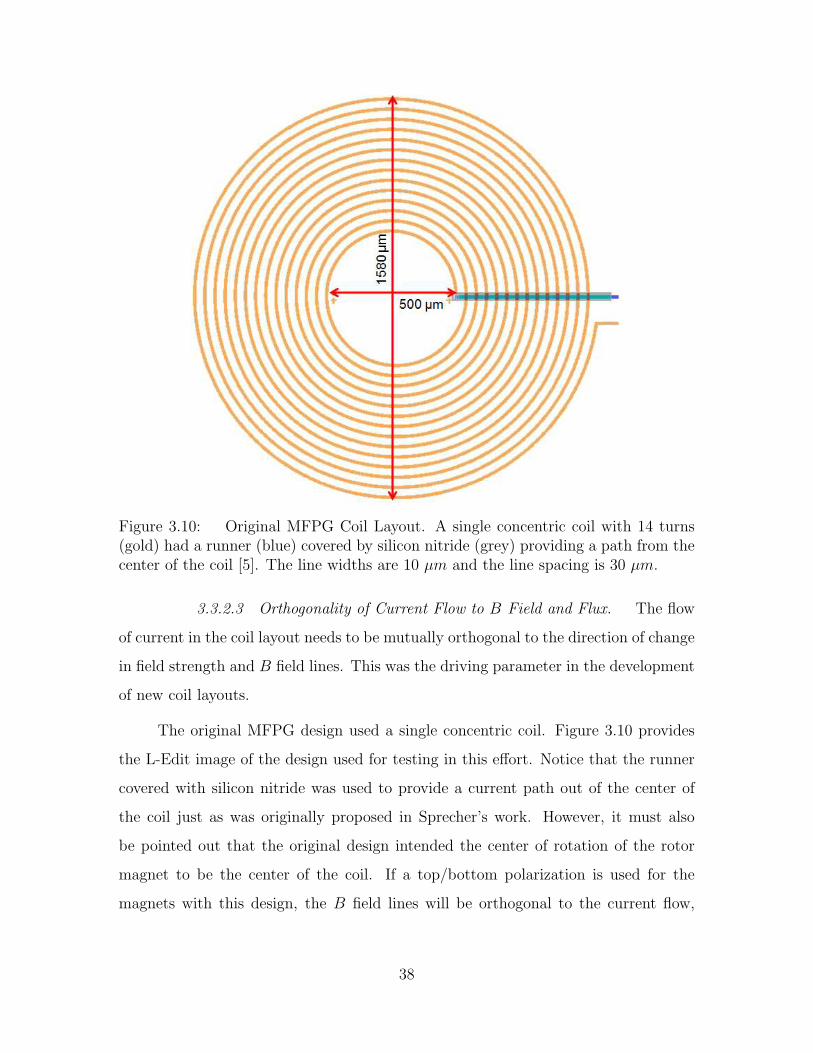
Figure 3.10: Original MFPG Coil Layout. A single concentric coil with 14 turns(gold) had a runner (blue) covered by silicon nitride (grey) providing a path from thecenter of the coil [5]. The line widths are 10 µm and the line spacing is 30 µm.
3.3.2.3 Orthogonality of Current Flow to B Field and Flux. The flow
of current in the coil layout needs to be mutually orthogonal to the direction of change
in field strength and B field lines. This was the driving parameter in the development
of new coil layouts.
The original MFPG design used a single concentric coil. Figure 3.10 provides
the L-Edit image of the design used for testing in this effort. Notice that the runner
covered with silicon nitride was used to provide a current path out of the center of
the coil just as was originally proposed in Sprecher’s work. However, it must also
be pointed out that the original design intended the center of rotation of the rotor
magnet to be the center of the coil. If a top/bottom polarization is used for the
magnets with this design, the B field lines will be orthogonal to the current flow,
38
however, the direction of the magnetic flux would be in the same direction as the
intended flow of current. As discussed earlier, this would lead to a less than optimal
current density, if any at all. The next two designs presented offer a variation of the
original MFPG design that should optimize the current density.
The object of the new design is to have the direction of current flow purely or-
thogonal to the direction of magnetic flux caused by the rotation of the rotor magnets.
In order to do this, the coil wires need to be aligned with radial lines from the center
of rotor rotation. This requirement led to a new design consisting of an intercon-
nected polar array of angular coils centered on the rotor magnets center of rotation.
Figures 3.11 (a) and (b) provide images of the angular coil designs developed using
L-Edit. As shown in Figure 3.11, the runner wire was covered by silicon nitride to
provide the current path from the center of the coils for both designs. The difference
between the two is simply the number of turns contained in each coil. Figure 3.11 (a)
contains 12 turns and (b) contains 6.
It turns out that the 6-turn angular coil aligns very well with the 4-arm toroidal
rotor as can be observed in Figure 3.6. It is anticipated that this combination of rotor
and coil placement will provide the highest power output of all potential combinations
of the rotors and coils presented in this chapter. In order to understand the reason
for such an assumption, one must recall the right-hand rule as it pertains to the
Ampere-Maxwell Law discussed at the beginning of this chapter. Using the right-
hand rule with the B fields at the edge of each magnet arm, such as those illustrated
in Figure 3.6, one can recognize those fields induce currents opposite in direction of
one another; the current on one side of the magnet flows in the opposite direction as
that on the other side of the arm. Therefore, optimally the arm will be the same size
as the coil, or very close, so that the currents are effectively combining for maximum
current density. If multiple magnets are covering one coil then the currents might
completely cancel with each other and the effective current flow would be zero.
39
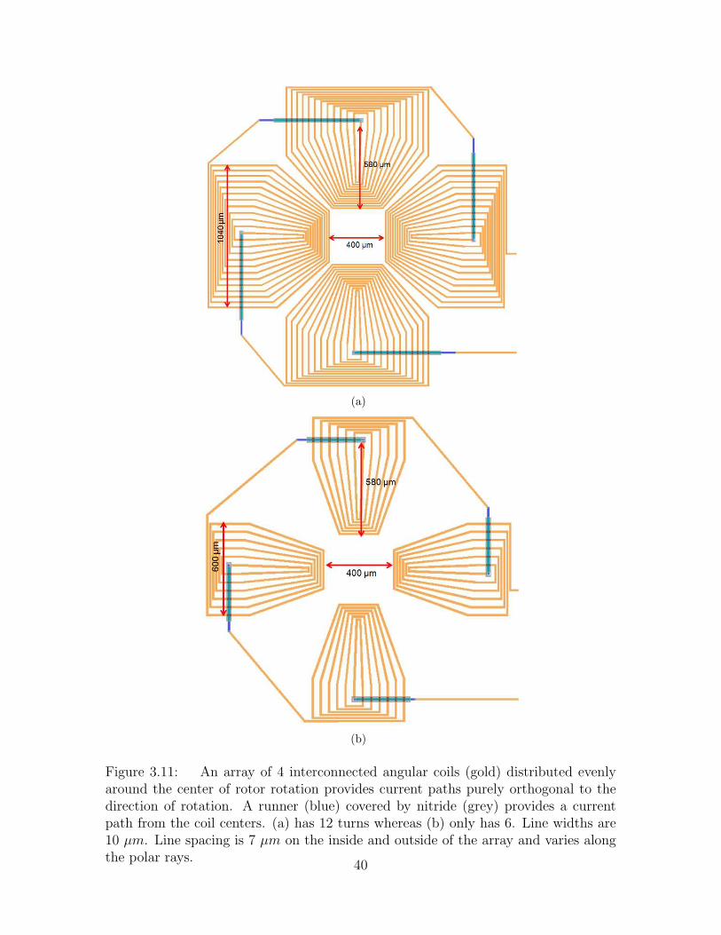
(a)
(b)
Figure 3.11: An array of 4 interconnected angular coils (gold) distributed evenlyaround the center of rotor rotation provides current paths purely orthogonal to thedirection of rotation. A runner (blue) covered by nitride (grey) provides a currentpath from the coil centers. (a) has 12 turns whereas (b) only has 6. Line widths are10 µm. Line spacing is 7 µm on the inside and outside of the array and varies alongthe polar rays.
40
3.4 Test Structure
The original MFPG design was intended to function using a turbine actuated by
blood flow in order to move the rotor. Such a design is very complicated and exceeds
the scope of this effort, therefore, in order to test the power output of the stator
coil and rotor magnet designs presented in this chapter, a test structure is required.
The general idea for the test structure is to align a rotor and an inverted coil within
close proximity, revolve the rotor, and measure the output current of the coil. The
test structure, therefore, needs to perform three main functions: provide a rotation
mechanism for the rotor, allow for precise alignment of rotor and coil, and measure
power output.
3.4.1 Rotation Mechanism. The testing apparatus should simulate the
rotation that might be provided by a turbine interfacing with blood flow. Sprecher
calculated the rotation rate provided by typical human blood flow to be approximately
39.3 RPM [5]. This rotation rate will serve as a starting point for the current research.
In addition, the rotation device needs to be able to provide a consistent planar surface
given that it will serve as a stage for the rotor and will be placed within tens of µm to
the stator coils. Any fluctuations could cause the stator and rotor to come in contact
and damage the devices.
Difficulty arises in finding a device that is accurate to such a slow rotation rate.
Devices considered included a photoresist application spinner, rotary stage for optics
tables, and a servo motor produced for a robot system built by LEGOTM Mindstorms
NXT. Spinners are typically only accurate to about 100 RPM. Optics table rotary
stages meet the rotation rate requirements and are excessively accurate but one was
not available for this research. The LEGOTM motor is available and provides a variable
RPM that meets the requirements.
3.4.2 Precise Alignment. The center of rotation of the rotor must be aligned
very accurately with the center of the stator design in order for correct functionality.
41
This requires a tool that can provide minute alterations in orientation in all 6 degrees
of freedom as well as imaging to verify alignment. Microstages, such as those fabri-
cated by Klinger Scientific, can provide such precise control of orientation within a
few microns. Multiple microstages are available and will be used in this effort.
Imaging is more complicated. Given that the stator and rotor must be in close
proximity, it is very difficult to see between them to observe if they are correctly
aligned. A solution is to take advantage of a system that is already designed for such
imaging. A flip-chip bonder uses a special optical tool to align two microelectronics
devices and bond them together. AFIT has an Eagle 860 flip-chip bonder. It is
expected that a custom stage with micro controls and rotation capability could be
built and used with the optics of this bonder. In order to facilitate with the alignment,
rotors and stators will both be fabricated and centered on small chips of the same
size, 5000× 5000 µm2.
3.4.3 Power Output Measurement. A technique for measuring the power
output of the device must be considered as well. Power is defined by
P =V 2
R(3.5)
where P is power in watts, V is voltage in volts, and R is resistance in ohms. In order
to measure the power output of any device, a predetermined load, or resistance, can
be placed in the circuit. The voltage drop across that load can be measured and,
using Equation 3.5, one can determine the power output of the system.
Therefore, in order to measure the power output of the micro-generator, a re-
sistor will be placed between the two electrodes of the coil. Two large gold pads
connected to the coil will be included on the stator chips to facilitate the measure-
ment. A wire bonder will connect a small wire to each pad and a resistor will be
placed between them. A multimeter will be used to measure the voltage drop across
the resistor and the power output will be determined using Equation 3.5 for multiple
42
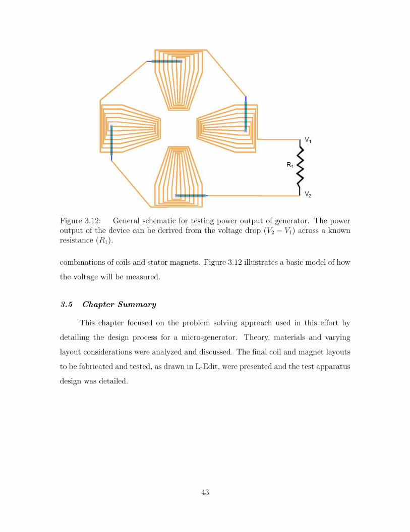
Figure 3.12: General schematic for testing power output of generator. The poweroutput of the device can be derived from the voltage drop (V2 − V1) across a knownresistance (R1).
combinations of coils and stator magnets. Figure 3.12 illustrates a basic model of how
the voltage will be measured.
3.5 Chapter Summary
This chapter focused on the problem solving approach used in this effort by
detailing the design process for a micro-generator. Theory, materials and varying
layout considerations were analyzed and discussed. The final coil and magnet layouts
to be fabricated and tested, as drawn in L-Edit, were presented and the test apparatus
design was detailed.
43
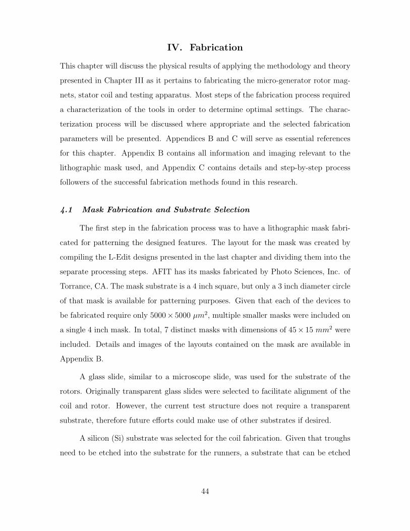
IV. Fabrication
This chapter will discuss the physical results of applying the methodology and theory
presented in Chapter III as it pertains to fabricating the micro-generator rotor mag-
nets, stator coil and testing apparatus. Most steps of the fabrication process required
a characterization of the tools in order to determine optimal settings. The charac-
terization process will be discussed where appropriate and the selected fabrication
parameters will be presented. Appendices B and C will serve as essential references
for this chapter. Appendix B contains all information and imaging relevant to the
lithographic mask used, and Appendix C contains details and step-by-step process
followers of the successful fabrication methods found in this research.
4.1 Mask Fabrication and Substrate Selection
The first step in the fabrication process was to have a lithographic mask fabri-
cated for patterning the designed features. The layout for the mask was created by
compiling the L-Edit designs presented in the last chapter and dividing them into the
separate processing steps. AFIT has its masks fabricated by Photo Sciences, Inc. of
Torrance, CA. The mask substrate is a 4 inch square, but only a 3 inch diameter circle
of that mask is available for patterning purposes. Given that each of the devices to
be fabricated require only 5000× 5000 µm2, multiple smaller masks were included on
a single 4 inch mask. In total, 7 distinct masks with dimensions of 45× 15 mm2 were
included. Details and images of the layouts contained on the mask are available in
Appendix B.
A glass slide, similar to a microscope slide, was used for the substrate of the
rotors. Originally transparent glass slides were selected to facilitate alignment of the
coil and rotor. However, the current test structure does not require a transparent
substrate, therefore future efforts could make use of other substrates if desired.
A silicon (Si) substrate was selected for the coil fabrication. Given that troughs
need to be etched into the substrate for the runners, a substrate that can be etched
44
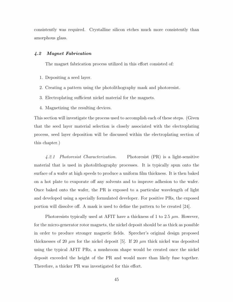
consistently was required. Crystalline silicon etches much more consistently than
amorphous glass.
4.2 Magnet Fabrication
The magnet fabrication process utilized in this effort consisted of:
1. Depositing a seed layer.
2. Creating a pattern using the photolithography mask and photoresist.
3. Electroplating sufficient nickel material for the magnets.
4. Magnetizing the resulting devices.
This section will investigate the process used to accomplish each of these steps. (Given
that the seed layer material selection is closely associated with the electroplating
process, seed layer deposition will be discussed within the electroplating section of
this chapter.)
4.2.1 Photoresist Characterization. Photoresist (PR) is a light-sensitive
material that is used in photolithography processes. It is typically spun onto the
surface of a wafer at high speeds to produce a uniform film thickness. It is then baked
on a hot plate to evaporate off any solvents and to improve adhesion to the wafer.
Once baked onto the wafer, the PR is exposed to a particular wavelength of light
and developed using a specially formulated developer. For positive PRs, the exposed
portion will dissolve off. A mask is used to define the pattern to be created [24].
Photoresists typically used at AFIT have a thickness of 1 to 2.5 µm. However,
for the micro-generator rotor magnets, the nickel deposit should be as thick as possible
in order to produce stronger magnetic fields. Sprecher’s original design proposed
thicknesses of 20 µm for the nickel deposit [5]. If 20 µm thick nickel was deposited
using the typical AFIT PRs, a mushroom shape would be created once the nickel
deposit exceeded the height of the PR and would more than likely fuse together.
Therefore, a thicker PR was investigated for this effort.
45
Figure 4.1: Spin Curve for AZ P4620. Provides associated thicknesses relative tospin speeds for the P4620 photoresist [25].
AZ P4620 is a PR produced by AZ Electronic Materials. It can be deposited to
thicknesses ranging from 3 to 60 µm [25]. This PR was selected to provide the pattern
for the nickel deposit. Figure 4.1 provides a chart mapping spin speed to thickness
for P4620.
The datasheet for this PR listed a double application process to acquire a 24 µm
thick film as well as a single application process that resulted in greater than 20 µm
thick film [25]. Both were investigated and the double application process was iden-
tified as the best choice given that it provided a more uniform and consistent PR
spread.
The datasheet also listed a recommended constant exposure dose of between
1500 mJ/cm2 to 1750 mJ/cm2 [25]. Through experimentation using AFIT’s EVG
620 mask aligner, it was found that this recommended dose was more than twice
what was actually needed. Figure 4.2 provides images of the results of two different
exposure doses. As can be observed in Figure 4.2 (a), the 1600 mJ/cm2 exposure
resulted in very rounded edges, indicative of over-exposure. A reduced exposure,
46
(a) (b)
Figure 4.2: Exposure comparison of AZ P4620 lithography patterns. The recom-mended fixed dose exposure was higher than what was required with AFIT’s EVG620 Mask Aligner. Using a fixed dose of 1600 mJ/cm2 resulted in very rounded edgesas represented in image (a). A fixed dose of 750 mJ/cm2 produced much sharperlines, represented in image (b).
shown Figure 4.2 (b), produced much cleaner lines. The optimal dosage was found to
be 680 mJ/cm2 with the EVG 620.
In addition, the high viscosity of the P4620 and the rectangular shape of the
substrate slides resulted in significant edge beading. Some beading was measured to
be 50% thicker than the center of the slide. With such variation in thickness a single
exposure and development time could not be used for the entirety of the slide. For
this reason only two rows of rotors were patterned in the center of each slide instead
of the three rows originally planned. Doing so successfully avoided the edge beads
and allowed for clean patterning. The entire process follower for the successful 24 µm
thick AZ P4620 application can be found in Appendix C.
4.2.2 Nickel Plating. This section will analyze the fabrication experiments
completed in order to characterize the nickel electroplating bath as well as discuss the
resulting process selected for the rotor magnet deposition.
47
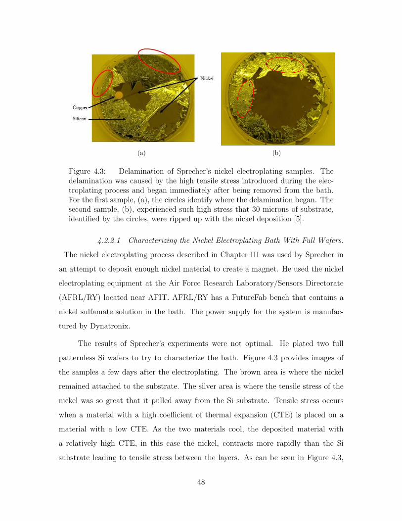
(a) (b)
Figure 4.3: Delamination of Sprecher’s nickel electroplating samples. Thedelamination was caused by the high tensile stress introduced during the elec-troplating process and began immediately after being removed from the bath.For the first sample, (a), the circles identify where the delamination began. Thesecond sample, (b), experienced such high stress that 30 microns of substrate,identified by the circles, were ripped up with the nickel deposition [5].
4.2.2.1 Characterizing the Nickel Electroplating Bath With Full Wafers.
The nickel electroplating process described in Chapter III was used by Sprecher in
an attempt to deposit enough nickel material to create a magnet. He used the nickel
electroplating equipment at the Air Force Research Laboratory/Sensors Directorate
(AFRL/RY) located near AFIT. AFRL/RY has a FutureFab bench that contains a
nickel sulfamate solution in the bath. The power supply for the system is manufac-
tured by Dynatronix.
The results of Sprecher’s experiments were not optimal. He plated two full
patternless Si wafers to try to characterize the bath. Figure 4.3 provides images of
the samples a few days after the electroplating. The brown area is where the nickel
remained attached to the substrate. The silver area is where the tensile stress of the
nickel was so great that it pulled away from the Si substrate. Tensile stress occurs
when a material with a high coefficient of thermal expansion (CTE) is placed on a
material with a low CTE. As the two materials cool, the deposited material with
a relatively high CTE, in this case the nickel, contracts more rapidly than the Si
substrate leading to tensile stress between the layers. As can be seen in Figure 4.3,
48
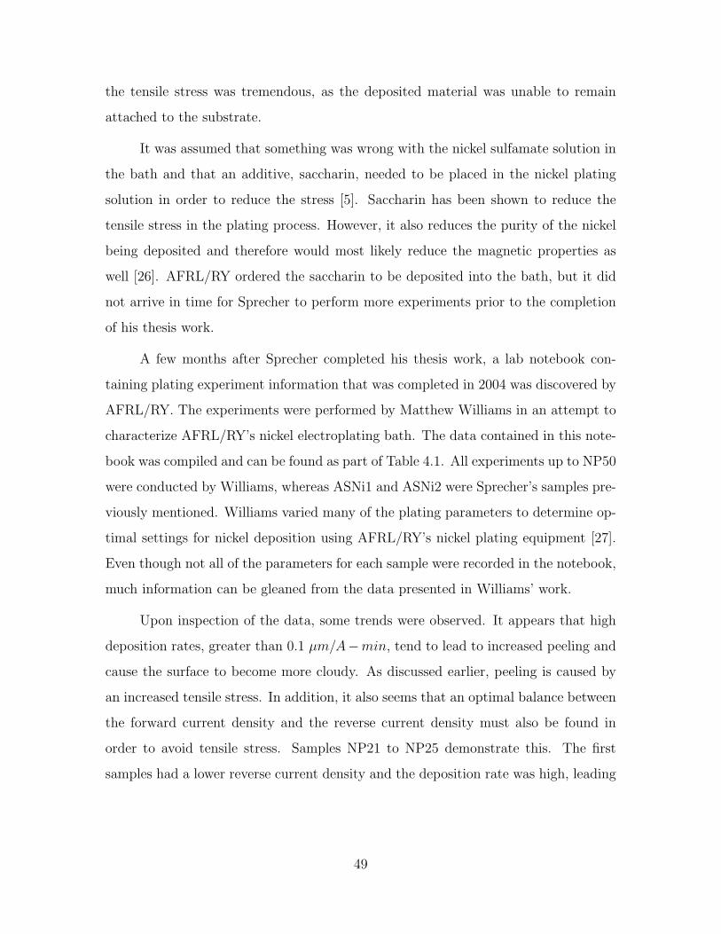
the tensile stress was tremendous, as the deposited material was unable to remain
attached to the substrate.
It was assumed that something was wrong with the nickel sulfamate solution in
the bath and that an additive, saccharin, needed to be placed in the nickel plating
solution in order to reduce the stress [5]. Saccharin has been shown to reduce the
tensile stress in the plating process. However, it also reduces the purity of the nickel
being deposited and therefore would most likely reduce the magnetic properties as
well [26]. AFRL/RY ordered the saccharin to be deposited into the bath, but it did
not arrive in time for Sprecher to perform more experiments prior to the completion
of his thesis work.
A few months after Sprecher completed his thesis work, a lab notebook con-
taining plating experiment information that was completed in 2004 was discovered by
AFRL/RY. The experiments were performed by Matthew Williams in an attempt to
characterize AFRL/RY’s nickel electroplating bath. The data contained in this note-
book was compiled and can be found as part of Table 4.1. All experiments up to NP50
were conducted by Williams, whereas ASNi1 and ASNi2 were Sprecher’s samples pre-
viously mentioned. Williams varied many of the plating parameters to determine op-
timal settings for nickel deposition using AFRL/RY’s nickel plating equipment [27].
Even though not all of the parameters for each sample were recorded in the notebook,
much information can be gleaned from the data presented in Williams’ work.
Upon inspection of the data, some trends were observed. It appears that high
deposition rates, greater than 0.1 µm/A−min, tend to lead to increased peeling and
cause the surface to become more cloudy. As discussed earlier, peeling is caused by
an increased tensile stress. In addition, it also seems that an optimal balance between
the forward current density and the reverse current density must also be found in
order to avoid tensile stress. Samples NP21 to NP25 demonstrate this. The first
samples had a lower reverse current density and the deposition rate was high, leading
49
Tab
le4.
1:N
icke
lE
lect
ropla
ting
Exper
imen
talD
ata
[5,2
7].
Yel
low
hig
hligh
ting
indic
ates
chan
ges
from
pre
vio
us
run.
50
to some peeling. However, as an optimal reverse current was approached, the peeling
stopped.
It was also noted that even though the deposition rate of NP26 was the same as
that of NP22, no peeling occurred with NP26 and it had a more uniform deposition.
This seems to indicate that the deposition rate might not be the best method of stress
control. There were two parameters that were changed between these two samples:
proximity to the anode and the reverse current. Further testing was required to
identify which parameter induced the high stress.
Williams also tried different seed layers. It appears, from the recorded data,
that there was not much difference between the 200 A Ti/2000 A Copper (Cu) seed
and the 200 A Ti/1000 A Ni seed. In fact the two runs with the least peeling and
shiniest surfaces were done with these two seeds, samples NP27 and NP33. AFIT
does not have the capability to deposit Cu, therefore the 200 A Ti/1000 A Ni will be
used as the seed for this effort.
After compiling this data and combining it with the results of Sprecher’s ex-
periments, samples ASNi1 and 2, some additional experiments were designed and
conducted by this author and some of the staff at AFRL/RY on full 3-inch wafers.
Table 4.1 contains the parameters from the most recent full wafer experiments as well,
NiStr1 to NiStr8. It must be noted that the saccharine additive was not added to the
solution before the most current experiments began. Therefore the solution that was
used by Sprecher and the solution that was used for the current sample set, NiStr1 - 8,
are the same.
Of the new batch of experiments, the most informative were NiStr3, NiStr4 and
NiStr6. NiStr3 had very little peeling. For NiStr4, two parameters were varied from
NiStr3, proximity to the anode and reverse current; similar to the variation of NP22
and NP26 previously mentioned. Serious peeling was observed with NiStr4. Sample
NiStr6 was an attempt to identify whether the excessive stress of NiStr4 was due to
moving the anode closer or reducing the reverse current. For NiStr6, the anode was
51
left in the normal position and only the reverse current was reduced. The stress was
still present. Therefore it is concluded that the stress is at least partially caused by the
change in reverse current. In addition, since moving the anode closer to the sample
should only increase the deposition rate (which can easily be varied by altering the
forward current), the anode should be left in the normal position for all additional
plating runs.
NiStr7a, NiStr7b, and NiStr8 were duplicates of previous processes in order
to verify that one could recreate the results of previous experiments. NiStr7a was a
duplicate of Sprecher’s work. The only difference was the seed layer. A nickel seed was
used instead of a chromium/copper seed. The results however were almost identical.
(An image was unavailable but it appeared very similar to Figure 4.3.) Upon closer
inspection of the parameters that were used and the deposition rate, one can recognize
that high stress would be expected. These parameters produce a deposition rate of
more than 0.4 µm/A−min and no reverse current was used.
NiStr7b and NiStr8 used the same process as NP27 and NP33, respectively, and
produced the best results seen during this round of experimentation. In addition, the
results mirrored Williams’ tests. Given that successful platings were accomplished
using the same bath but different parameters, it was determined that the saccharine
additive was not needed to reduce the stress. Images of the wafers after the electro-
plating process can be seen in Figure 4.4. The forward and reverse current densities
used for these wafers (17.5 mA/cm2 and 11.5 mA/cm2) will be the starting point for
the parameters to be used on the patterned samples discussed in the next section.
In summary, lessons learned from characterizing AFRL/RY’s nickel plating bath
with full size wafers include:
1. High stress deposits lead to delamination of the nickel deposit.
2. 200 A Ti/1000 A Ni provides a good seed layer for nickel and will be used as
the seed for this effort.
52
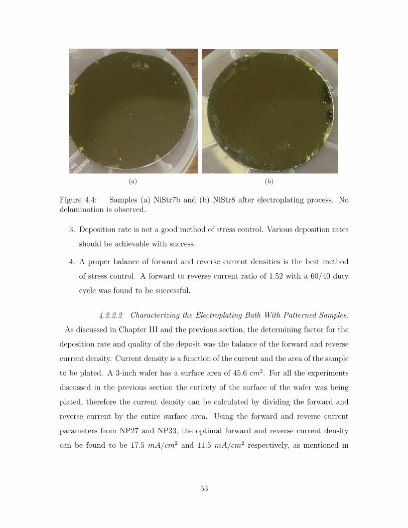
(a) (b)
Figure 4.4: Samples (a) NiStr7b and (b) NiStr8 after electroplating process. Nodelamination is observed.
3. Deposition rate is not a good method of stress control. Various deposition rates
should be achievable with success.
4. A proper balance of forward and reverse current densities is the best method
of stress control. A forward to reverse current ratio of 1.52 with a 60/40 duty
cycle was found to be successful.
4.2.2.2 Characterizing the Electroplating Bath With Patterned Samples.
As discussed in Chapter III and the previous section, the determining factor for the
deposition rate and quality of the deposit was the balance of the forward and reverse
current density. Current density is a function of the current and the area of the sample
to be plated. A 3-inch wafer has a surface area of 45.6 cm2. For all the experiments
discussed in the previous section the entirety of the surface of the wafer was being
plated, therefore the current density can be calculated by dividing the forward and
reverse current by the entire surface area. Using the forward and reverse current
parameters from NP27 and NP33, the optimal forward and reverse current density
can be found to be 17.5 mA/cm2 and 11.5 mA/cm2 respectively, as mentioned in
53
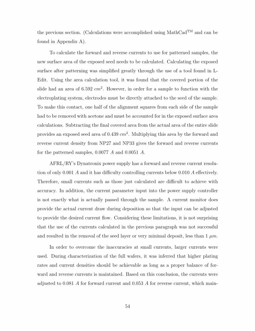
the previous section. (Calculations were accomplished using MathCadTM and can be
found in Appendix A).
To calculate the forward and reverse currents to use for patterned samples, the
new surface area of the exposed seed needs to be calculated. Calculating the exposed
surface after patterning was simplified greatly through the use of a tool found in L-
Edit. Using the area calculation tool, it was found that the covered portion of the
slide had an area of 6.592 cm2. However, in order for a sample to function with the
electroplating system, electrodes must be directly attached to the seed of the sample.
To make this contact, one half of the alignment squares from each side of the sample
had to be removed with acetone and must be accounted for in the exposed surface area
calculations. Subtracting the final covered area from the actual area of the entire slide
provides an exposed seed area of 0.439 cm2. Multiplying this area by the forward and
reverse current density from NP27 and NP33 gives the forward and reverse currents
for the patterned samples, 0.0077 A and 0.0051 A.
AFRL/RY’s Dynatronix power supply has a forward and reverse current resolu-
tion of only 0.001 A and it has difficulty controlling currents below 0.010 A effectively.
Therefore, small currents such as those just calculated are difficult to achieve with
accuracy. In addition, the current parameter input into the power supply controller
is not exactly what is actually passed through the sample. A current monitor does
provide the actual current draw during deposition so that the input can be adjusted
to provide the desired current flow. Considering these limitations, it is not surprising
that the use of the currents calculated in the previous paragraph was not successful
and resulted in the removal of the seed layer or very minimal deposit, less than 1 µm.
In order to overcome the inaccuracies at small currents, larger currents were
used. During characterization of the full wafers, it was inferred that higher plating
rates and current densities should be achievable as long as a proper balance of for-
ward and reverse currents is maintained. Based on this conclusion, the currents were
adjusted to 0.081 A for forward current and 0.053 A for reverse current, which main-
54
Figure 4.5: SEM image of successfully plated toroidal rotor. This rotor is 8 µmthick and no peeling is observed.
tains the ratio of forward to reverse current previously found of 1.52. These currents
lead to current densities of 182 mA/cm2 and 121 mA/cm2 respectively. The resulting
deposition rate was approximately 0.4 µm/min and no peeling or discoloration was
observed. Figure 4.5 provides a scanning electron microscope (SEM) image of one
of the successfully electroplated rotors resulting from this process. The variation in
plating thickness across the slide was significant, however, resulting in rotors with
thicknesses of up to 14 µm on the edges and only 7 µm thick in the middle.
In an effort to reduce the thickness variation, the reverse current was slightly
increased relative to the forward current leading to a forward/reverse ratio of 1.463,
with forward current at 0.06 A and reverse current at 0.041 A. Peeling was once
again observed. Figure 4.6 provides an SEM image of the resulting delamination. It
appears even slight changes in the forward to reverse ratio will affect the stress of the
deposit.
Given that the ratio needs to stay the same, it appears that an appropriate
method to reduce the variation in thicknesses would be to use a different shaped sam-
ple. The rectangular samples used in this effort allowed for one electrode attachment
on each end and lead to high current densities on the edges near the electrodes and
smaller current densities toward the center of the sample. Round samples would al-
55
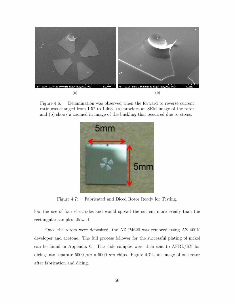
(a) (b)
Figure 4.6: Delamination was observed when the forward to reverse currentratio was changed from 1.52 to 1.463. (a) provides an SEM image of the rotorand (b) shows a zoomed in image of the buckling that occurred due to stress.
Figure 4.7: Fabricated and Diced Rotor Ready for Testing.
low the use of four electrodes and would spread the current more evenly than the
rectangular samples allowed.
Once the rotors were deposited, the AZ P4620 was removed using AZ 400K
developer and acetone. The full process follower for the successful plating of nickel
can be found in Appendix C. The slide samples were then sent to AFRL/RY for
dicing into separate 5000 µm × 5000 µm chips. Figure 4.7 is an image of one rotor
after fabrication and dicing.
56
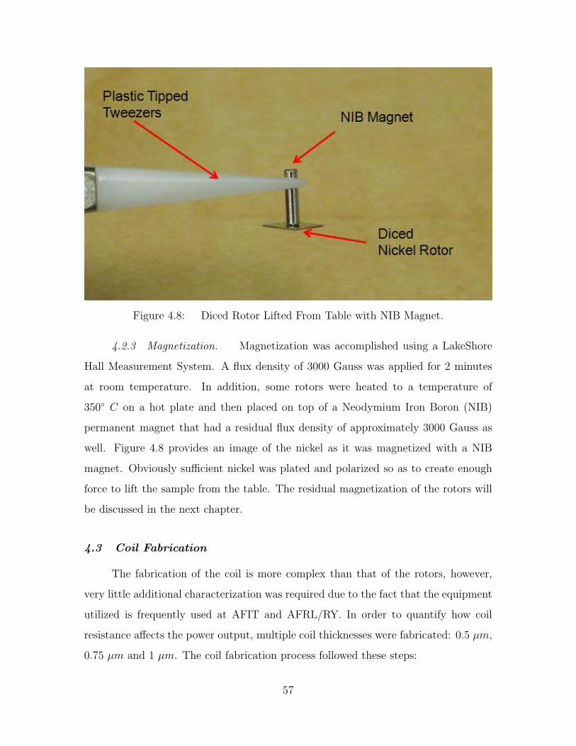
Figure 4.8: Diced Rotor Lifted From Table with NIB Magnet.
4.2.3 Magnetization. Magnetization was accomplished using a LakeShore
Hall Measurement System. A flux density of 3000 Gauss was applied for 2 minutes
at room temperature. In addition, some rotors were heated to a temperature of
350 C on a hot plate and then placed on top of a Neodymium Iron Boron (NIB)
permanent magnet that had a residual flux density of approximately 3000 Gauss as
well. Figure 4.8 provides an image of the nickel as it was magnetized with a NIB
magnet. Obviously sufficient nickel was plated and polarized so as to create enough
force to lift the sample from the table. The residual magnetization of the rotors will
be discussed in the next chapter.
4.3 Coil Fabrication
The fabrication of the coil is more complex than that of the rotors, however,
very little additional characterization was required due to the fact that the equipment
utilized is frequently used at AFIT and AFRL/RY. In order to quantify how coil
resistance affects the power output, multiple coil thicknesses were fabricated: 0.5 µm,
0.75 µm and 1 µm. The coil fabrication process followed these steps:
57
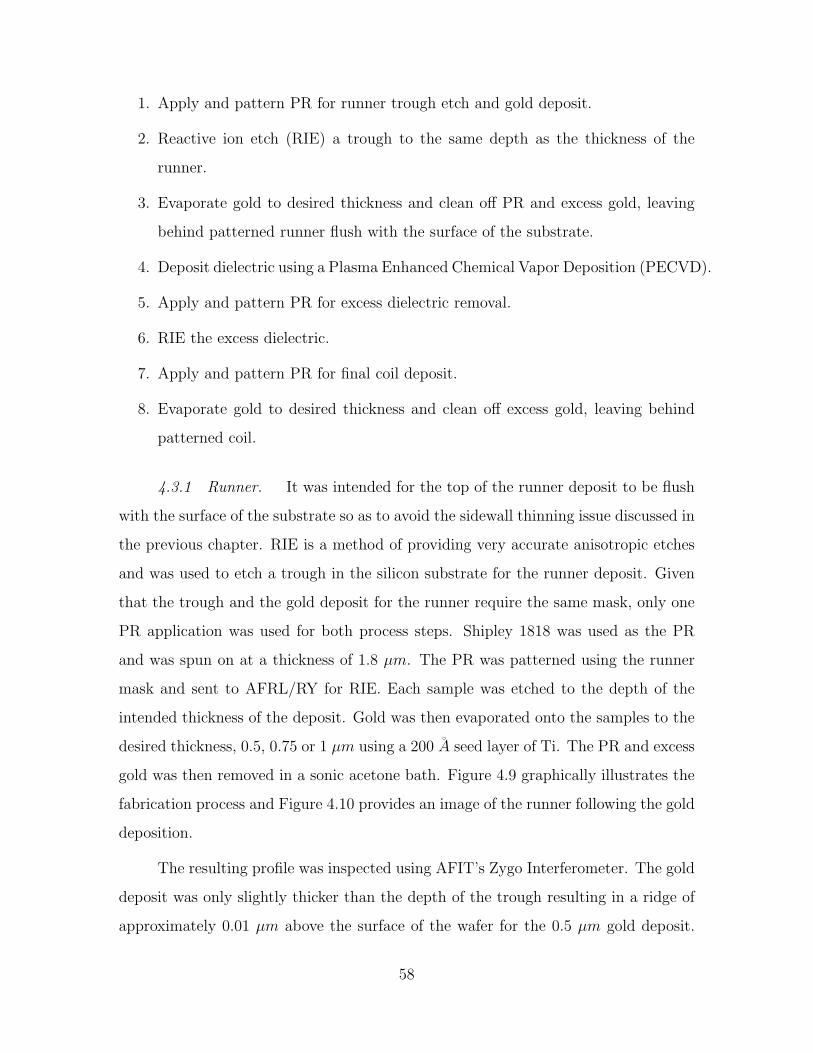
1. Apply and pattern PR for runner trough etch and gold deposit.
2. Reactive ion etch (RIE) a trough to the same depth as the thickness of the
runner.
3. Evaporate gold to desired thickness and clean off PR and excess gold, leaving
behind patterned runner flush with the surface of the substrate.
4. Deposit dielectric using a Plasma Enhanced Chemical Vapor Deposition (PECVD).
5. Apply and pattern PR for excess dielectric removal.
6. RIE the excess dielectric.
7. Apply and pattern PR for final coil deposit.
8. Evaporate gold to desired thickness and clean off excess gold, leaving behind
patterned coil.
4.3.1 Runner. It was intended for the top of the runner deposit to be flush
with the surface of the substrate so as to avoid the sidewall thinning issue discussed in
the previous chapter. RIE is a method of providing very accurate anisotropic etches
and was used to etch a trough in the silicon substrate for the runner deposit. Given
that the trough and the gold deposit for the runner require the same mask, only one
PR application was used for both process steps. Shipley 1818 was used as the PR
and was spun on at a thickness of 1.8 µm. The PR was patterned using the runner
mask and sent to AFRL/RY for RIE. Each sample was etched to the depth of the
intended thickness of the deposit. Gold was then evaporated onto the samples to the
desired thickness, 0.5, 0.75 or 1 µm using a 200 A seed layer of Ti. The PR and excess
gold was then removed in a sonic acetone bath. Figure 4.9 graphically illustrates the
fabrication process and Figure 4.10 provides an image of the runner following the gold
deposition.
The resulting profile was inspected using AFIT’s Zygo Interferometer. The gold
deposit was only slightly thicker than the depth of the trough resulting in a ridge of
approximately 0.01 µm above the surface of the wafer for the 0.5 µm gold deposit.
58
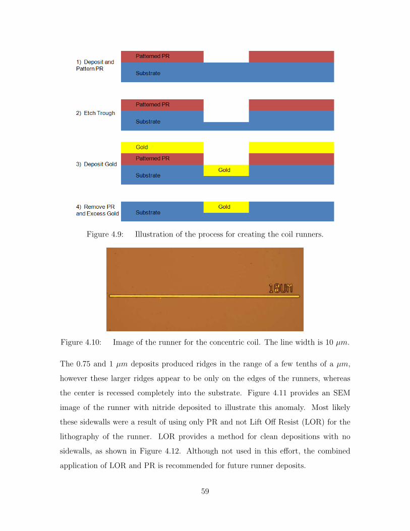
Figure 4.9: Illustration of the process for creating the coil runners.
Figure 4.10: Image of the runner for the concentric coil. The line width is 10 µm.
The 0.75 and 1 µm deposits produced ridges in the range of a few tenths of a µm,
however these larger ridges appear to be only on the edges of the runners, whereas
the center is recessed completely into the substrate. Figure 4.11 provides an SEM
image of the runner with nitride deposited to illustrate this anomaly. Most likely
these sidewalls were a result of using only PR and not Lift Off Resist (LOR) for the
lithography of the runner. LOR provides a method for clean depositions with no
sidewalls, as shown in Figure 4.12. Although not used in this effort, the combined
application of LOR and PR is recommended for future runner deposits.
59
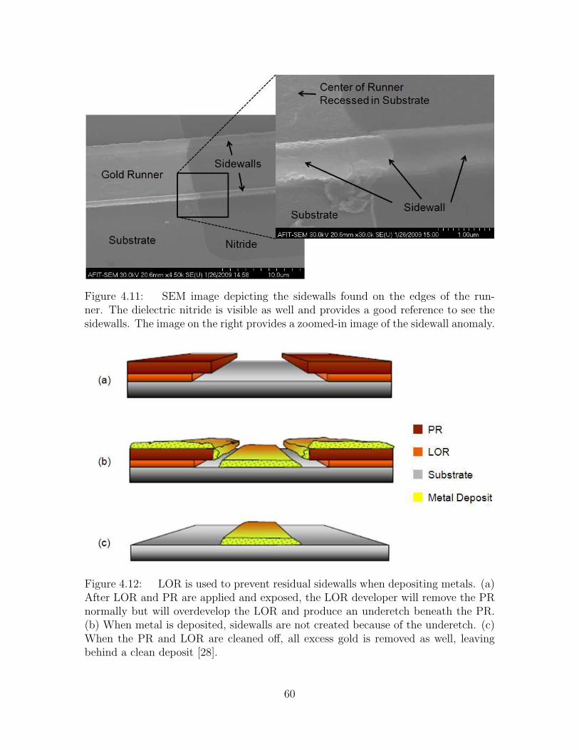
Figure 4.11: SEM image depicting the sidewalls found on the edges of the run-ner. The dielectric nitride is visible as well and provides a good reference to see thesidewalls. The image on the right provides a zoomed-in image of the sidewall anomaly.
Figure 4.12: LOR is used to prevent residual sidewalls when depositing metals. (a)After LOR and PR are applied and exposed, the LOR developer will remove the PRnormally but will overdevelop the LOR and produce an underetch beneath the PR.(b) When metal is deposited, sidewalls are not created because of the underetch. (c)When the PR and LOR are cleaned off, all excess gold is removed as well, leavingbehind a clean deposit [28].
60
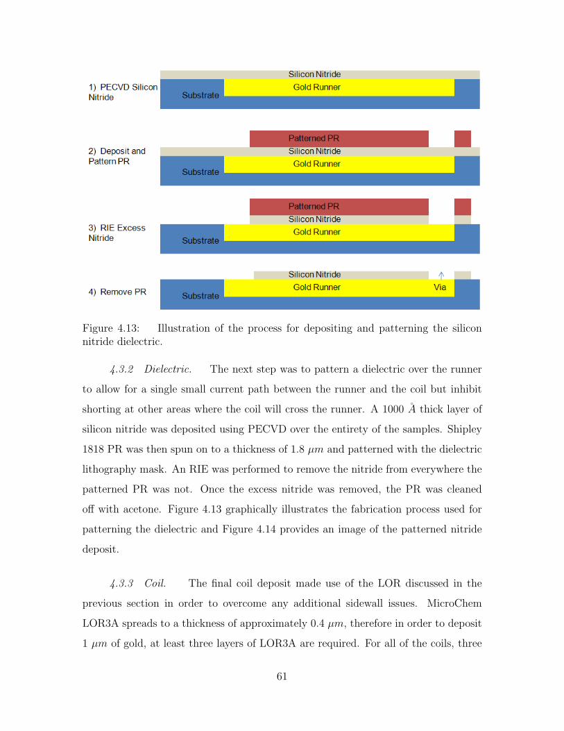
Figure 4.13: Illustration of the process for depositing and patterning the siliconnitride dielectric.
4.3.2 Dielectric. The next step was to pattern a dielectric over the runner
to allow for a single small current path between the runner and the coil but inhibit
shorting at other areas where the coil will cross the runner. A 1000 A thick layer of
silicon nitride was deposited using PECVD over the entirety of the samples. Shipley
1818 PR was then spun on to a thickness of 1.8 µm and patterned with the dielectric
lithography mask. An RIE was performed to remove the nitride from everywhere the
patterned PR was not. Once the excess nitride was removed, the PR was cleaned
off with acetone. Figure 4.13 graphically illustrates the fabrication process used for
patterning the dielectric and Figure 4.14 provides an image of the patterned nitride
deposit.
4.3.3 Coil. The final coil deposit made use of the LOR discussed in the
previous section in order to overcome any additional sidewall issues. MicroChem
LOR3A spreads to a thickness of approximately 0.4 µm, therefore in order to deposit
1 µm of gold, at least three layers of LOR3A are required. For all of the coils, three
61
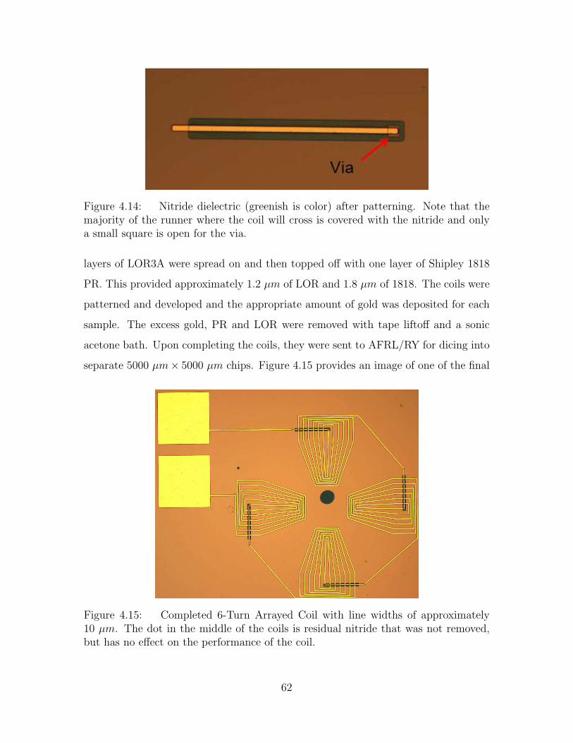
Figure 4.14: Nitride dielectric (greenish is color) after patterning. Note that themajority of the runner where the coil will cross is covered with the nitride and onlya small square is open for the via.
layers of LOR3A were spread on and then topped off with one layer of Shipley 1818
PR. This provided approximately 1.2 µm of LOR and 1.8 µm of 1818. The coils were
patterned and developed and the appropriate amount of gold was deposited for each
sample. The excess gold, PR and LOR were removed with tape liftoff and a sonic
acetone bath. Upon completing the coils, they were sent to AFRL/RY for dicing into
separate 5000 µm× 5000 µm chips. Figure 4.15 provides an image of one of the final
Figure 4.15: Completed 6-Turn Arrayed Coil with line widths of approximately10 µm. The dot in the middle of the coils is residual nitride that was not removed,but has no effect on the performance of the coil.
62
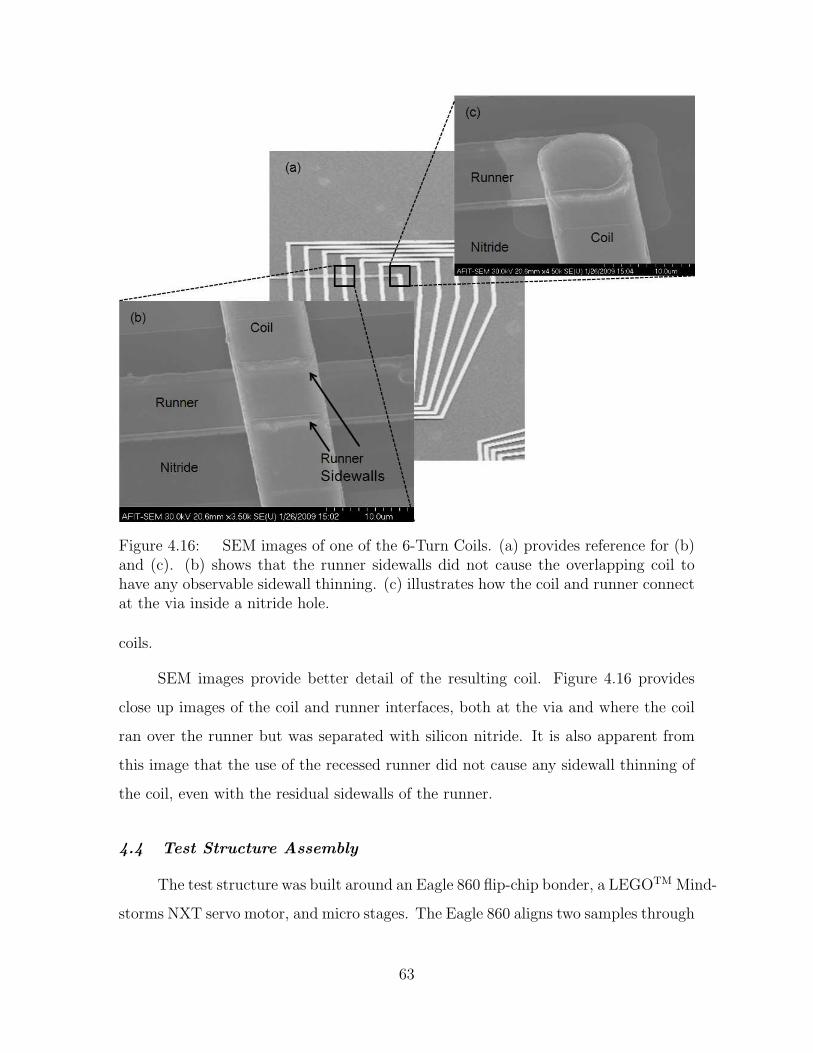
Figure 4.16: SEM images of one of the 6-Turn Coils. (a) provides reference for (b)and (c). (b) shows that the runner sidewalls did not cause the overlapping coil tohave any observable sidewall thinning. (c) illustrates how the coil and runner connectat the via inside a nitride hole.
coils.
SEM images provide better detail of the resulting coil. Figure 4.16 provides
close up images of the coil and runner interfaces, both at the via and where the coil
ran over the runner but was separated with silicon nitride. It is also apparent from
this image that the use of the recessed runner did not cause any sidewall thinning of
the coil, even with the residual sidewalls of the runner.
4.4 Test Structure Assembly
The test structure was built around an Eagle 860 flip-chip bonder, a LEGOTM Mind-
storms NXT servo motor, and micro stages. The Eagle 860 aligns two samples through
63
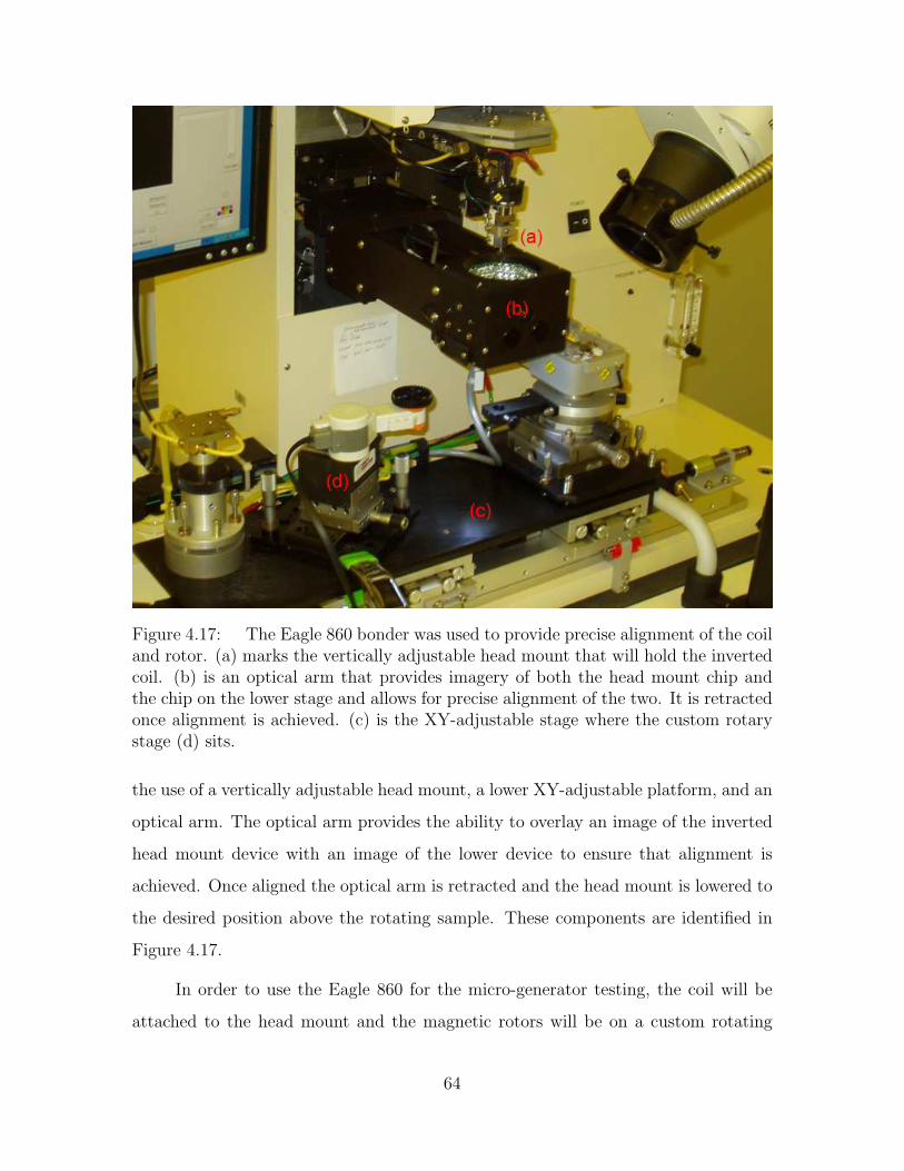
Figure 4.17: The Eagle 860 bonder was used to provide precise alignment of the coiland rotor. (a) marks the vertically adjustable head mount that will hold the invertedcoil. (b) is an optical arm that provides imagery of both the head mount chip andthe chip on the lower stage and allows for precise alignment of the two. It is retractedonce alignment is achieved. (c) is the XY-adjustable stage where the custom rotarystage (d) sits.
the use of a vertically adjustable head mount, a lower XY-adjustable platform, and an
optical arm. The optical arm provides the ability to overlay an image of the inverted
head mount device with an image of the lower device to ensure that alignment is
achieved. Once aligned the optical arm is retracted and the head mount is lowered to
the desired position above the rotating sample. These components are identified in
Figure 4.17.
In order to use the Eagle 860 for the micro-generator testing, the coil will be
attached to the head mount and the magnetic rotors will be on a custom rotating
64
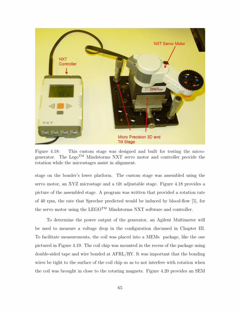
Figure 4.18: This custom stage was designed and built for testing the micro-generator. The LegoTM Mindstorms NXT servo motor and controller provide therotation while the microstages assist in alignment.
stage on the bonder’s lower platform. The custom stage was assembled using the
servo motor, an XYZ microstage and a tilt adjustable stage. Figure 4.18 provides a
picture of the assembled stage. A program was written that provided a rotation rate
of 40 rpm, the rate that Sprecher predicted would be induced by blood-flow [5], for
the servo motor using the LEGOTM Mindstorms NXT software and controller.
To determine the power output of the generator, an Agilent Multimeter will
be used to measure a voltage drop in the configuration discussed in Chapter III.
To facilitate measurements, the coil was placed into a MEMs package, like the one
pictured in Figure 4.19. The coil chip was mounted in the recess of the package using
double-sided tape and wire bonded at AFRL/RY. It was important that the bonding
wires be tight to the surface of the coil chip so as to not interfere with rotation when
the coil was brought in close to the rotating magnets. Figure 4.20 provides an SEM
65
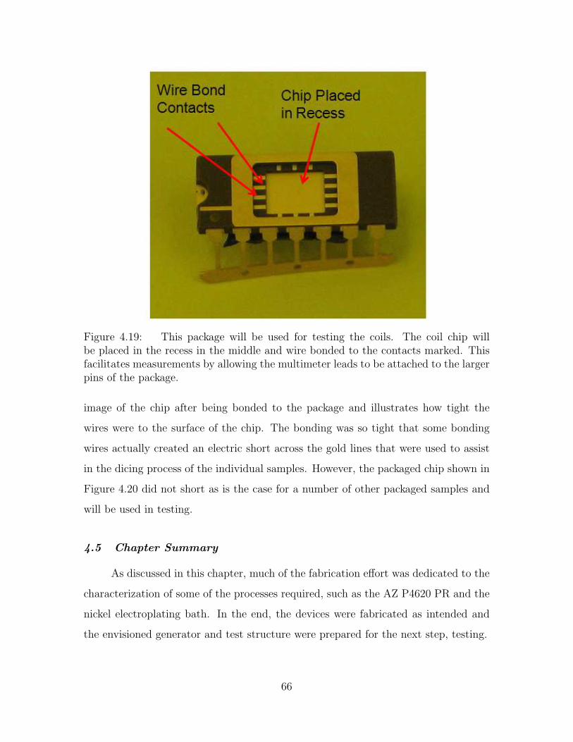
Figure 4.19: This package will be used for testing the coils. The coil chip willbe placed in the recess in the middle and wire bonded to the contacts marked. Thisfacilitates measurements by allowing the multimeter leads to be attached to the largerpins of the package.
image of the chip after being bonded to the package and illustrates how tight the
wires were to the surface of the chip. The bonding was so tight that some bonding
wires actually created an electric short across the gold lines that were used to assist
in the dicing process of the individual samples. However, the packaged chip shown in
Figure 4.20 did not short as is the case for a number of other packaged samples and
will be used in testing.
4.5 Chapter Summary
As discussed in this chapter, much of the fabrication effort was dedicated to the
characterization of some of the processes required, such as the AZ P4620 PR and the
nickel electroplating bath. In the end, the devices were fabricated as intended and
the envisioned generator and test structure were prepared for the next step, testing.
66
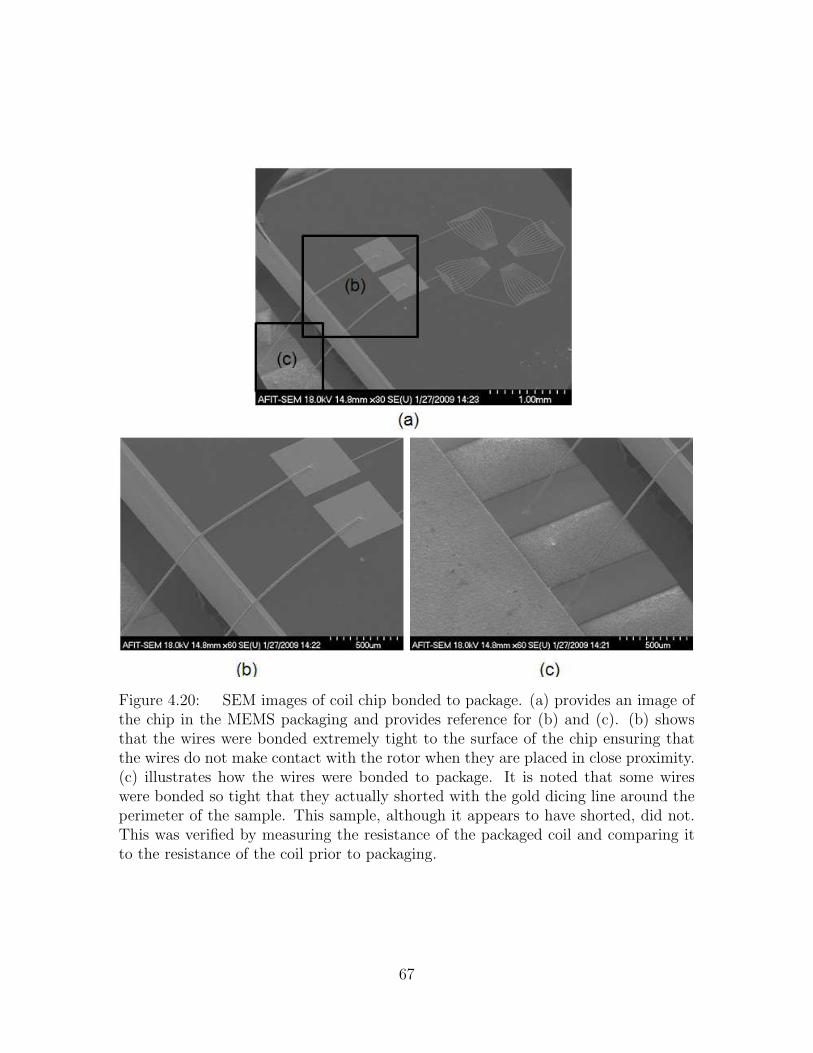
Figure 4.20: SEM images of coil chip bonded to package. (a) provides an image ofthe chip in the MEMS packaging and provides reference for (b) and (c). (b) showsthat the wires were bonded extremely tight to the surface of the chip ensuring thatthe wires do not make contact with the rotor when they are placed in close proximity.(c) illustrates how the wires were bonded to package. It is noted that some wireswere bonded so tight that they actually shorted with the gold dicing line around theperimeter of the sample. This sample, although it appears to have shorted, did not.This was verified by measuring the resistance of the packaged coil and comparing itto the resistance of the coil prior to packaging.
67
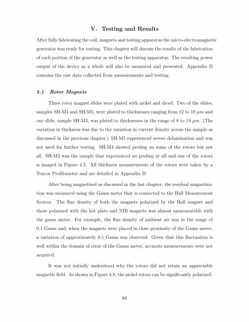
V. Testing and Results
After fully fabricating the coil, magnets and testing apparatus the micro-electromagnetic
generator was ready for testing. This chapter will discuss the results of the fabrication
of each portion of the generator as well as the testing apparatus. The resulting power
output of the device as a whole will also be measured and presented. Appendix D
contains the raw data collected from measurements and testing.
5.1 Rotor Magnets
Three rotor magnet slides were plated with nickel and diced. Two of the slides,
samples SH-M4 and SH-M5, were plated to thicknesses ranging from 12 to 18 µm and
one slide, sample SH-M3, was plated to thicknesses in the range of 8 to 14 µm. (The
variation in thickness was due to the variation in current density across the sample as
discussed in the previous chapter.) SH-M5 experienced severe delamination and was
not used for further testing. SH-M4 showed peeling on some of the rotors but not
all. SH-M3 was the sample that experienced no peeling at all and one of the rotors
is imaged in Figure 4.5. All thickness measurements of the rotors were taken by a
Tencor Profilometer and are detailed in Appendix D.
After being magnetized as discussed in the last chapter, the residual magnetiza-
tion was measured using the Gauss meter that is connected to the Hall Measurement
System. The flux density of both the magnets polarized by the Hall magnet and
those polarized with the hot plate and NIB magnets was almost unmeasurable with
the gauss meter. For example, the flux density of ambient air was in the range of
0.1 Gauss and, when the magnets were placed in close proximity of the Gauss meter,
a variation of approximately 0.1 Gauss was observed. Given that this fluctuation is
well within the domain of error of the Gauss meter, accurate measurements were not
acquired.
It was not initially understood why the rotors did not retain an appreciable
magnetic field. As shown in Figure 4.8, the nickel rotors can be significantly polarized.
68
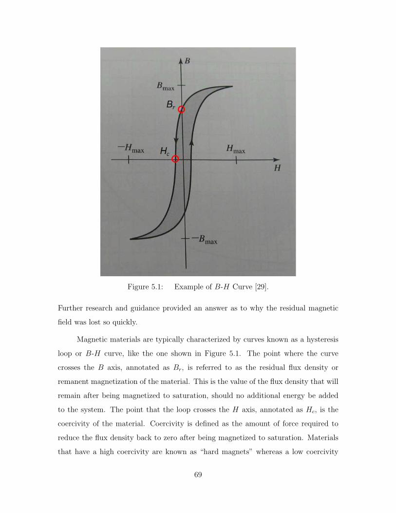
Figure 5.1: Example of B-H Curve [29].
Further research and guidance provided an answer as to why the residual magnetic
field was lost so quickly.
Magnetic materials are typically characterized by curves known as a hysteresis
loop or B-H curve, like the one shown in Figure 5.1. The point where the curve
crosses the B axis, annotated as Br, is referred to as the residual flux density or
remanent magnetization of the material. This is the value of the flux density that will
remain after being magnetized to saturation, should no additional energy be added
to the system. The point that the loop crosses the H axis, annotated as Hc, is the
coercivity of the material. Coercivity is defined as the amount of force required to
reduce the flux density back to zero after being magnetized to saturation. Materials
that have a high coercivity are known as “hard magnets” whereas a low coercivity
69
material is referred to as a “soft magnet”. In addition, coercivity is typically higher
for materials that have defects in their atomic structures. Although, the defects also
cause a reduction in the flux density [18,29,30].
These two values, coercivity and remanent flux density, are extremely important
for the magnetic material in a electromagnetic generator. Obviously, a high remanent
flux density is desired to induce maximum current in the conducting coil, but a high
coercivity is desired as well so that ambient energy and forces, such as small bumps
and temperature changes, do not demagnetize the magnet. Permanent magnets are
permanent due to their extremely high coercivity values.
The coercivity of the electroplated nickel rotors was measured with a Vibrat-
ing Sample Magnetometer (VSM) at the Air Force Research Laboratory/Propulsion
Directorate (AFRL/RZ). Figure 5.2 contains the resulting B-H curve with the coer-
civity circled. The coercivity was measured to be approximately 90 Oersteds. The
low end of permanent magnets have a coercivity of 2,000 to 3,000 Oersteds [30]. It
Figure 5.2: B-H curve for electroplated nickel rotors measured with a VSM.
70
turns out that all nickel, no matter how it is deposited, produces very soft magnets, as
does annealed iron. Even though these materials are capable of acquiring a powerful
remanent flux density, they cannot maintain that density as they experience external
forces. This is the reason that the nickel magnets exhibited high magnetic flux char-
acteristics when placed near the NIB magnets but the flux was imperceptible when
measurement was attempted. The movement of the samples with the tweezers was
evidently sufficient energy to randomize the poles that had just been polarized.
5.2 Stator Coils
The goal in fabricating the coils was to create a low resistance electrical path
that would be mutually orthogonal to the B field and varying flux density. In total,
six slides of coils completed the fabrication process: two slides of each of the desired
thicknesses, 0.5, 0.75, and 1 µm. The first step for determining how well the coils
were fabricated was to measure the resistance of the coils. Resistances were taken
using an Agilent multimeter connected to the two pads on each coil. The results of
those measurements can be found in Table D.2.
As discussed in the design portion of this thesis, the line widths of all of the coils
was intended to be 10 µm. However, when fabricating at this scale, variations are
typical. For this reason and to determine how well calculated resistance values match
to experimental results, a Tencor Profilometer at AFRL/RY was used to attempt to
measure the average final line widths and thicknesses of each type of coil on each
slide sample. With that data, the resistances were calculated and compared with the
average of the reasonable measured values in Table 5.1.
As can be observed in Table 5.1 and Table D.2, the majority of the 0.5 µm coils
and a few of the 0.75 and 1 µm coils exhibited extremely high resistance values. A
conclusive reason for such a high resistance was not found. One potential reason is
that some residual PR was present prior to the final gold coil deposit. This would
result in a barrier of PR between the coil and runner and would increase the resistance.
The discrepancies in the other predicted and experimental results were attributed to
71
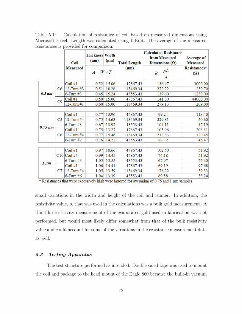
Table 5.1: Calculation of resistance of coil based on measured dimensions usingMicrosoft Excel. Length was calculated using L-Edit. The average of the measuredresistances is provided for comparison.
small variations in the width and height of the coil and runner. In addition, the
resistivity value, ρ, that was used in the calculations was a bulk gold measurement. A
thin film resistivity measurement of the evaporated gold used in fabrication was not
performed, but would most likely differ somewhat from that of the bulk resistivity
value and could account for some of the variations in the resistance measurement data
as well.
5.3 Testing Apparatus
The test structure performed as intended. Double sided tape was used to mount
the coil and package to the head mount of the Eagle 860 because the built-in vacuum
72
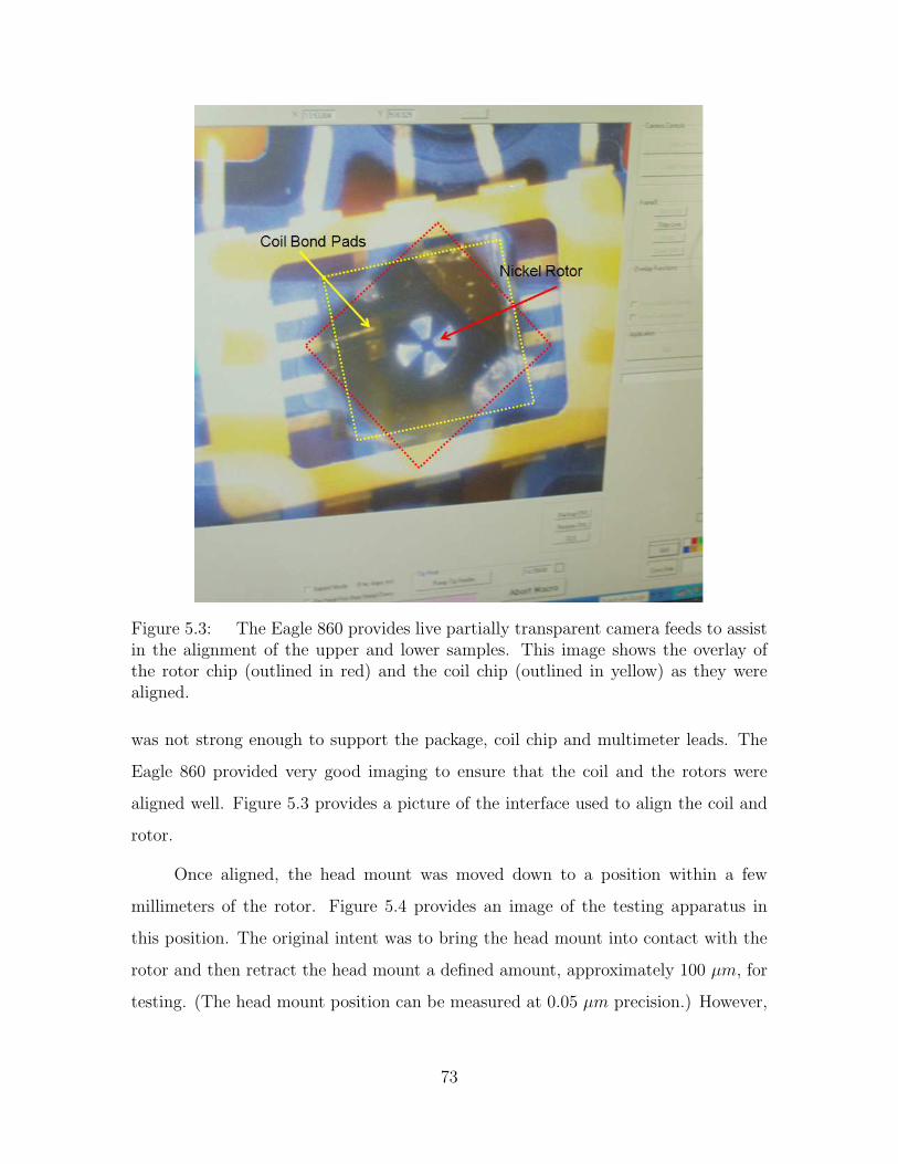
Figure 5.3: The Eagle 860 provides live partially transparent camera feeds to assistin the alignment of the upper and lower samples. This image shows the overlay ofthe rotor chip (outlined in red) and the coil chip (outlined in yellow) as they werealigned.
was not strong enough to support the package, coil chip and multimeter leads. The
Eagle 860 provided very good imaging to ensure that the coil and the rotors were
aligned well. Figure 5.3 provides a picture of the interface used to align the coil and
rotor.
Once aligned, the head mount was moved down to a position within a few
millimeters of the rotor. Figure 5.4 provides an image of the testing apparatus in
this position. The original intent was to bring the head mount into contact with the
rotor and then retract the head mount a defined amount, approximately 100 µm, for
testing. (The head mount position can be measured at 0.05 µm precision.) However,
73
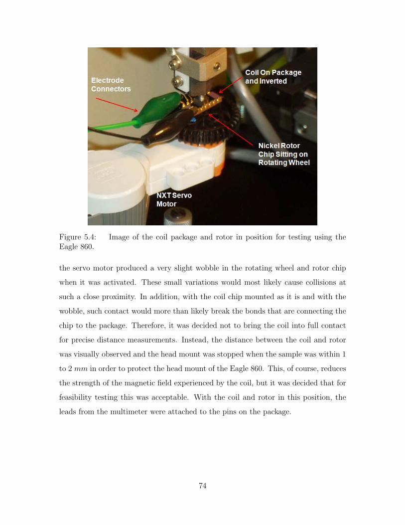
Figure 5.4: Image of the coil package and rotor in position for testing using theEagle 860.
the servo motor produced a very slight wobble in the rotating wheel and rotor chip
when it was activated. These small variations would most likely cause collisions at
such a close proximity. In addition, with the coil chip mounted as it is and with the
wobble, such contact would more than likely break the bonds that are connecting the
chip to the package. Therefore, it was decided not to bring the coil into full contact
for precise distance measurements. Instead, the distance between the coil and rotor
was visually observed and the head mount was stopped when the sample was within 1
to 2 mm in order to protect the head mount of the Eagle 860. This, of course, reduces
the strength of the magnetic field experienced by the coil, but it was decided that for
feasibility testing this was acceptable. With the coil and rotor in this position, the
leads from the multimeter were attached to the pins on the package.
74
5.4 Micro-Generator
A 10 KΩ resistor was used as the load to measure the power output of the
generator. The Agilent Multimeter has an AC voltage precision of 0.001 mV . Using
this setting, no voltage drop was observed for any of the coils or magnets. Given that
the magnets were not retaining their flux density due to the “softness” of the nickel,
this was not surprising.
However, in order to verify that no current was being produced, a Keithley
PicoAmmeter was used to measure the current output of the device. The picoammeter
has a current measurement resolution of 2 nA. The resistor was removed from the
circuit and the leads were attached to each electrode for current measurements. No
current was measured in this configuration either.
5.5 Chapter Summary
This chapter presented the results of measuring and testing the rotor and coil of
the micro-generator as well as the generator as a whole. In addition, a discussion of
the functionality and process of using the testing apparatus was included. With the
failure of the nickel magnets, the micro-generator was unable to produce a measurable
current or voltage.
75

VI. Conclusions
This chapter will begin by providing a summary of the scientific contributions made
during this effort. In addition, recommendations for future work based upon the
lessons learned during this research will be presented.
6.1 Scientific Contributions
First and foremost, this thesis has shown that the use of electroplated nickel as
a magnetic rotor for a micro-electromagnetic generator is not feasible. However, the
new designs of the rotors and coils presented in this thesis provide a solid basis for
future efforts in developing a micro-electromagnetic generator. The angular coil and
toroidal rotor design meet the electromagnetic orientation requirements to properly
induce current flow for a generator. Simply switching the material being deposited
for the rotors would lead to the fabrication of a working generator.
The trough and runner deposition process is also a very important finding of
this thesis. It was shown that one could successfully overlay evaporated wires without
concern of thinning sidewalls. While it is true that the thinning sidewalls could be
avoided by sputtering the metal deposit instead of using evaporation, sputtering is
not always desired for some applications. Therefore, this finding allows the use of the
optimal deposition method for the application when wires must be overlayed.
6.2 Lessons Learned and Recommendations
In an effort to facilitate future research in this field, some recommendations for
follow-on research are provided here. These recommendations are derived from the
difficulties experienced in this research and from ideas that were not tested due to
time constraints.
6.2.1 Sample Selection. Due to the rectangular shape of the samples used for
this effort, it was very difficult to achieve a consistent PR spread for patterning. This
in turn lead to varying levels of PR thicknesses across the sample and thus varying
76
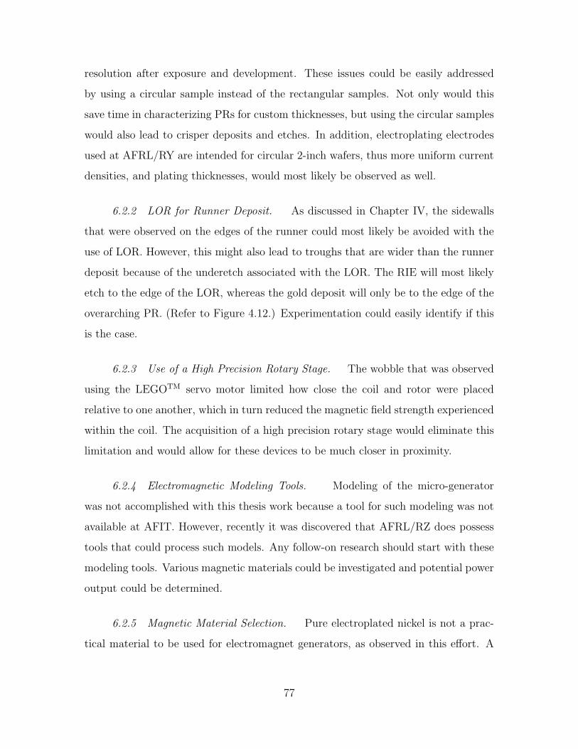
resolution after exposure and development. These issues could be easily addressed
by using a circular sample instead of the rectangular samples. Not only would this
save time in characterizing PRs for custom thicknesses, but using the circular samples
would also lead to crisper deposits and etches. In addition, electroplating electrodes
used at AFRL/RY are intended for circular 2-inch wafers, thus more uniform current
densities, and plating thicknesses, would most likely be observed as well.
6.2.2 LOR for Runner Deposit. As discussed in Chapter IV, the sidewalls
that were observed on the edges of the runner could most likely be avoided with the
use of LOR. However, this might also lead to troughs that are wider than the runner
deposit because of the underetch associated with the LOR. The RIE will most likely
etch to the edge of the LOR, whereas the gold deposit will only be to the edge of the
overarching PR. (Refer to Figure 4.12.) Experimentation could easily identify if this
is the case.
6.2.3 Use of a High Precision Rotary Stage. The wobble that was observed
using the LEGOTM servo motor limited how close the coil and rotor were placed
relative to one another, which in turn reduced the magnetic field strength experienced
within the coil. The acquisition of a high precision rotary stage would eliminate this
limitation and would allow for these devices to be much closer in proximity.
6.2.4 Electromagnetic Modeling Tools. Modeling of the micro-generator
was not accomplished with this thesis work because a tool for such modeling was not
available at AFIT. However, recently it was discovered that AFRL/RZ does possess
tools that could process such models. Any follow-on research should start with these
modeling tools. Various magnetic materials could be investigated and potential power
output could be determined.
6.2.5 Magnetic Material Selection. Pure electroplated nickel is not a prac-
tical material to be used for electromagnet generators, as observed in this effort. A
77
sputtered nickel deposit might result in more defects and thus a higher coercivity.
Optimally, though, a known permanent magnet material such as steel alloys or rare-
earth magnets (neodymium and samarium-cobalt) would be used. In order to use
one of these materials, a MEMS and IC compatible micro-deposition and pattern-
ing process would need to be identified [18]. Engineers at AFRL/RZ did say that
materials such as NIB have been deposited via sputtering and pulse laser deposi-
tion (PLD) [30]. However, with sputtering and PLD, a method of etching the excess
material is required as well. Obviously, more research is needed in this area.
6.2.6 Turbine Integration, Packaging and Power Conditioning. Once the
micro-generator is shown to produce power during rotation, the remaining parts of
the MFPG device would need to be fully designed, fabricated and tested. Additional
areas of research include: the fabrication of a turbine and a process for attaching it
to the rotor, fully fabricating a package to safely contain the generator while at the
same time allowing blood flow to actuate the turbines, and a method for conditioning
the power output of the generator for use with IC circuitry.
6.2.7 Piezoelectric Research. In Chapter 2, energy harvesting through the
use of piezoelectric materials was briefly discussed. A piezoelectric solution for har-
vesting ambient energy seems to offer many advantages to that of using an electro-
magnetic generator. Firstly, piezoelectric harvesters require minimal movement for
power generation, whereas an electromagnet generator generally requires significant
mechanical motion in order to induce current flow. By reducing the amount of me-
chanical motion, one increases the lifespan of the device and reduces the complexities
of design. In addition the power output potential of piezoelectrics are on par with
those of electromagnetic generators [9, 12]. Lastly, piezoelectrics could potentially
harvest the ambient kinetic energy of vibrations in almost any part of the body,
eliminating the need to place the device in bloodflow as was the intention of the
micro-electromagnetic generator. Additional research into the methods of depositing
78
piezoelectrics at the microscopic level could lead to exciting and very useful techniques
of harvesting ambient energy of bio-implanted devices.
6.3 Conclusion
A working micro-generator, such as the one envisioned in this thesis, would
lead to a new paradigm of power generation and a revolution in the possibilities of
biomedical engineering. There is no doubt that research should be continued. If
one could identify a method of depositing a rare-earth magnetic material in a MEMS
compatible manner, the designs presented here would provide the remaining processes
to create the active portion of a micro-generator.
79
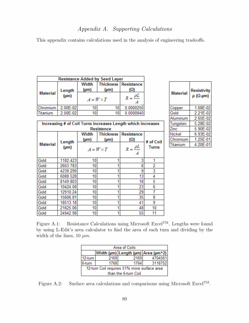
Appendix A. Supporting Calculations
This appendix contains calculations used in the analysis of engineering tradeoffs.
Figure A.1: Resistance Calculations using Microsoft ExcelTM. Lengths were foundby using L-Edit’s area calculator to find the area of each turn and dividing by thewidth of the lines, 10 µm.
Figure A.2: Surface area calculations and comparisons using Microsoft ExcelTM.
80
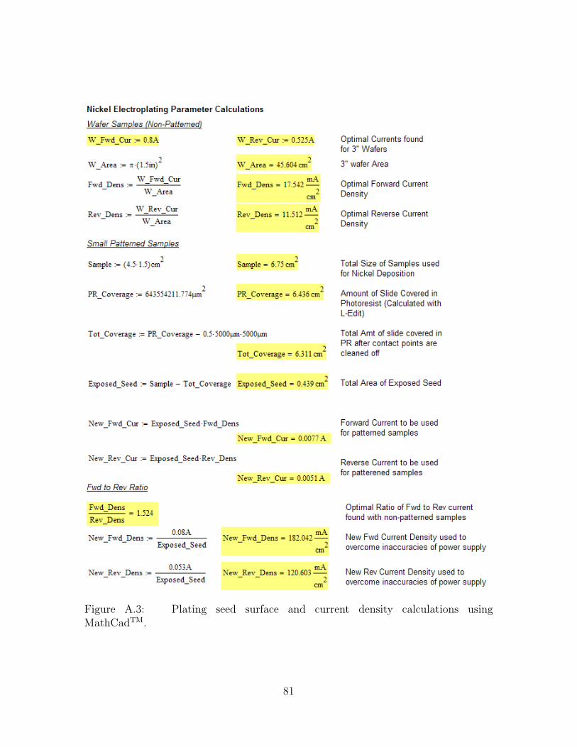
Figure A.3: Plating seed surface and current density calculations usingMathCadTM.
81
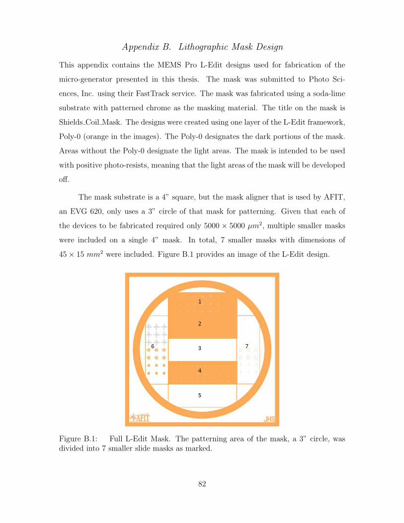
Appendix B. Lithographic Mask Design
This appendix contains the MEMS Pro L-Edit designs used for fabrication of the
micro-generator presented in this thesis. The mask was submitted to Photo Sci-
ences, Inc. using their FastTrack service. The mask was fabricated using a soda-lime
substrate with patterned chrome as the masking material. The title on the mask is
Shields Coil Mask. The designs were created using one layer of the L-Edit framework,
Poly-0 (orange in the images). The Poly-0 designates the dark portions of the mask.
Areas without the Poly-0 designate the light areas. The mask is intended to be used
with positive photo-resists, meaning that the light areas of the mask will be developed
off.
The mask substrate is a 4” square, but the mask aligner that is used by AFIT,
an EVG 620, only uses a 3” circle of that mask for patterning. Given that each of
the devices to be fabricated required only 5000 × 5000 µm2, multiple smaller masks
were included on a single 4” mask. In total, 7 smaller masks with dimensions of
45× 15 mm2 were included. Figure B.1 provides an image of the L-Edit design.
Figure B.1: Full L-Edit Mask. The patterning area of the mask, a 3” circle, wasdivided into 7 smaller slide masks as marked.
82
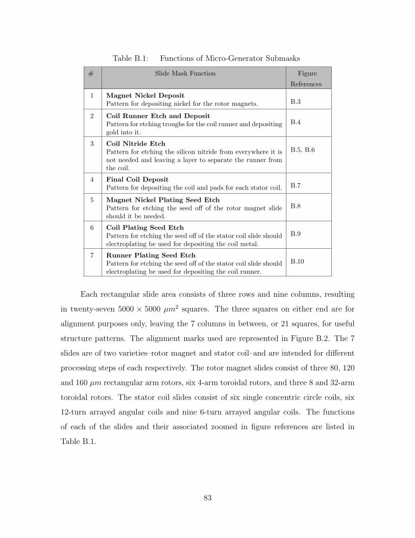
Table B.1: Functions of Micro-Generator Submasks
# Slide Mask Function Figure
References
1 Magnet Nickel DepositPattern for depositing nickel for the rotor magnets. B.3
2 Coil Runner Etch and DepositPattern for etching troughs for the coil runner and depositinggold into it.
B.4
3 Coil Nitride EtchPattern for etching the silicon nitride from everywhere it isnot needed and leaving a layer to separate the runner fromthe coil.
B.5, B.6
4 Final Coil DepositPattern for depositing the coil and pads for each stator coil. B.7
5 Magnet Nickel Plating Seed EtchPattern for etching the seed off of the rotor magnet slideshould it be needed.
B.8
6 Coil Plating Seed EtchPattern for etching the seed off of the stator coil slide shouldelectroplating be used for depositing the coil metal.
B.9
7 Runner Plating Seed EtchPattern for etching the seed off of the stator coil slide shouldelectroplating be used for depositing the coil runner.
B.10
Each rectangular slide area consists of three rows and nine columns, resulting
in twenty-seven 5000 × 5000 µm2 squares. The three squares on either end are for
alignment purposes only, leaving the 7 columns in between, or 21 squares, for useful
structure patterns. The alignment marks used are represented in Figure B.2. The 7
slides are of two varieties–rotor magnet and stator coil–and are intended for different
processing steps of each respectively. The rotor magnet slides consist of three 80, 120
and 160 µm rectangular arm rotors, six 4-arm toroidal rotors, and three 8 and 32-arm
toroidal rotors. The stator coil slides consist of six single concentric circle coils, six
12-turn arrayed angular coils and nine 6-turn arrayed angular coils. The functions
of each of the slides and their associated zoomed in figure references are listed in
Table B.1.
83
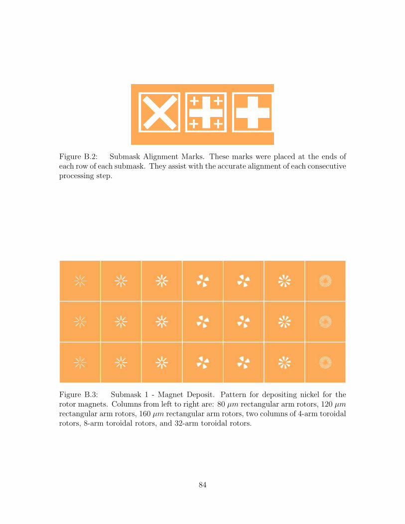
Figure B.2: Submask Alignment Marks. These marks were placed at the ends ofeach row of each submask. They assist with the accurate alignment of each consecutiveprocessing step.
Figure B.3: Submask 1 - Magnet Deposit. Pattern for depositing nickel for therotor magnets. Columns from left to right are: 80 µm rectangular arm rotors, 120 µmrectangular arm rotors, 160 µm rectangular arm rotors, two columns of 4-arm toroidalrotors, 8-arm toroidal rotors, and 32-arm toroidal rotors.
84
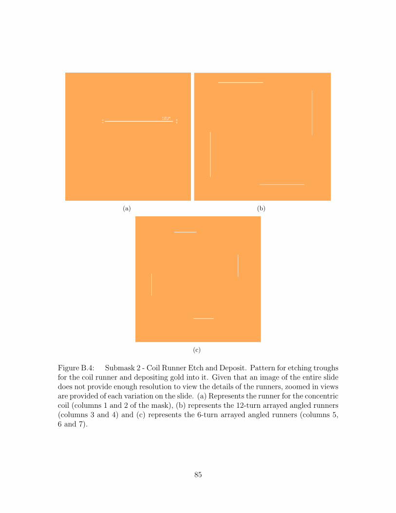
(a) (b)
(c)
Figure B.4: Submask 2 - Coil Runner Etch and Deposit. Pattern for etching troughsfor the coil runner and depositing gold into it. Given that an image of the entire slidedoes not provide enough resolution to view the details of the runners, zoomed in viewsare provided of each variation on the slide. (a) Represents the runner for the concentriccoil (columns 1 and 2 of the mask), (b) represents the 12-turn arrayed angled runners(columns 3 and 4) and (c) represents the 6-turn arrayed angled runners (columns 5,6 and 7).
85
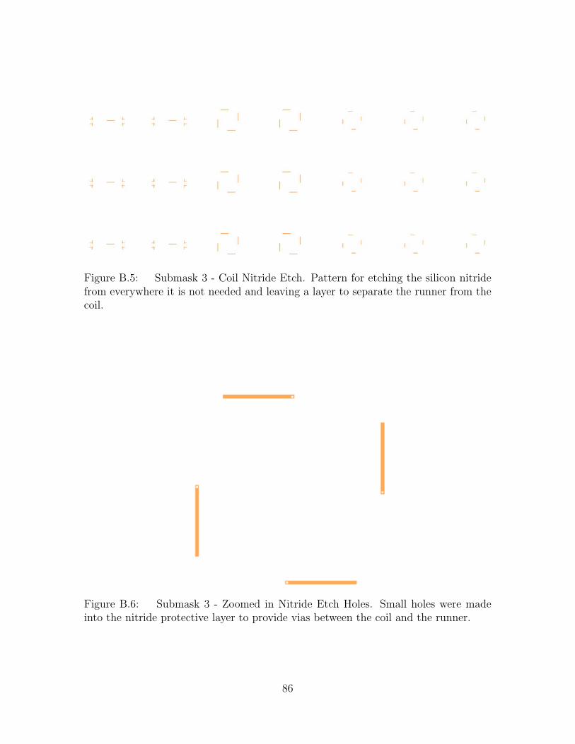
Figure B.5: Submask 3 - Coil Nitride Etch. Pattern for etching the silicon nitridefrom everywhere it is not needed and leaving a layer to separate the runner from thecoil.
Figure B.6: Submask 3 - Zoomed in Nitride Etch Holes. Small holes were madeinto the nitride protective layer to provide vias between the coil and the runner.
86
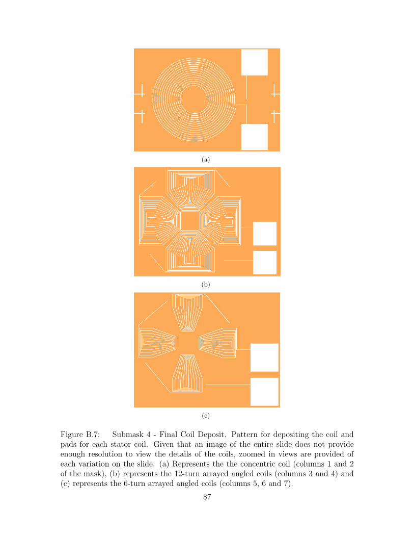
(a)
(b)
(c)
Figure B.7: Submask 4 - Final Coil Deposit. Pattern for depositing the coil andpads for each stator coil. Given that an image of the entire slide does not provideenough resolution to view the details of the coils, zoomed in views are provided ofeach variation on the slide. (a) Represents the the concentric coil (columns 1 and 2of the mask), (b) represents the 12-turn arrayed angled coils (columns 3 and 4) and(c) represents the 6-turn arrayed angled coils (columns 5, 6 and 7).
87
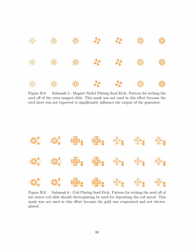
Figure B.8: Submask 5 - Magnet Nickel Plating Seed Etch. Pattern for etching theseed off of the rotor magnet slide. This mask was not used in this effort because theseed layer was not expected to significantly influence the output of the generator.
Figure B.9: Submask 6 - Coil Plating Seed Etch. Pattern for etching the seed off ofthe stator coil slide should electroplating be used for depositing the coil metal. Thismask was not used in this effort because the gold was evaporated and not electro-plated.
88
Figure B.10: Submask 7 - Runner Plating Seed Etch. Pattern for etching theseed off of the stator coil slide should electroplating be used for depositing the coilrunner. This mask was not used in this effort because the gold was evaporated andnot electroplated.
89
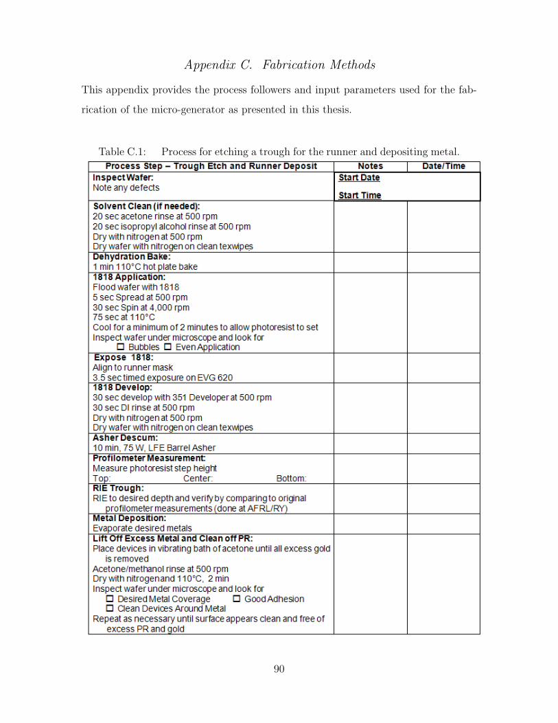
Appendix C. Fabrication Methods
This appendix provides the process followers and input parameters used for the fab-
rication of the micro-generator as presented in this thesis.
Table C.1: Process for etching a trough for the runner and depositing metal.
90
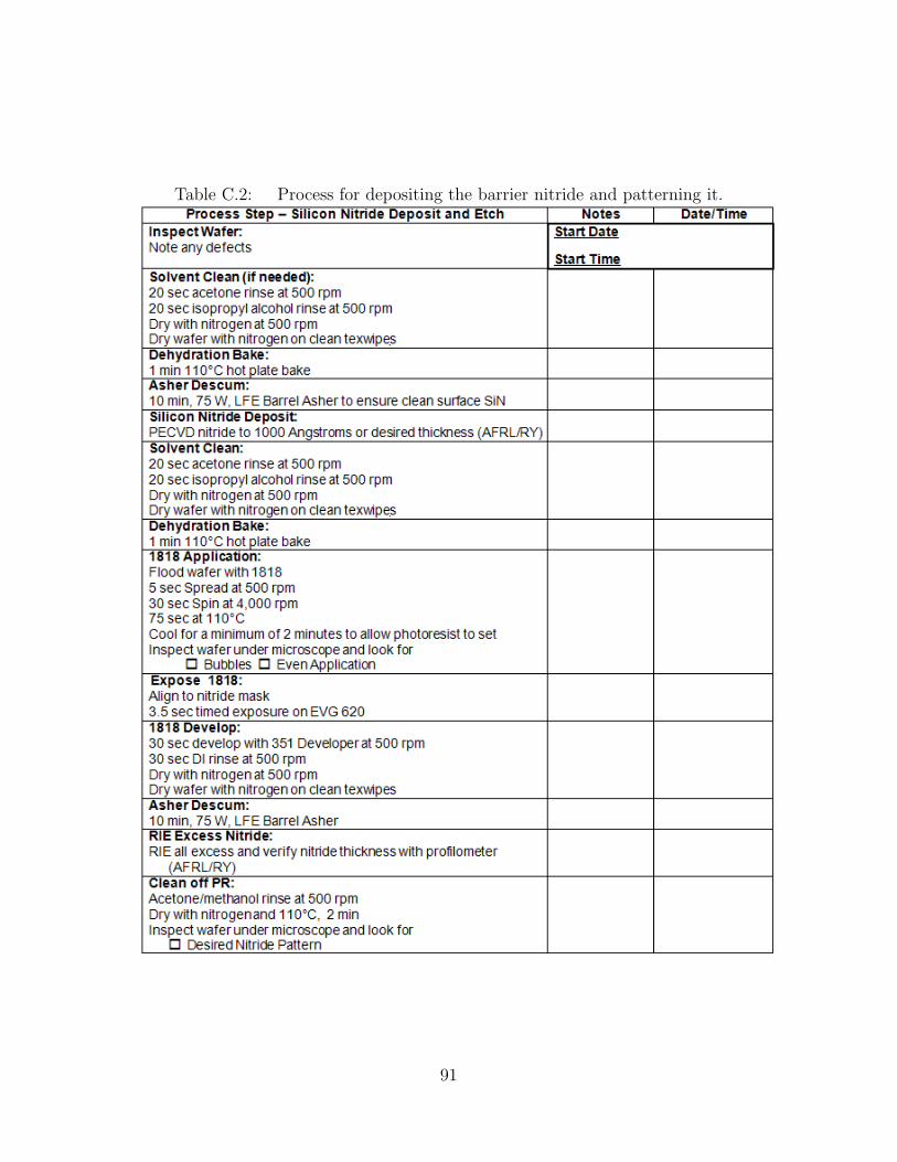
Table C.2: Process for depositing the barrier nitride and patterning it.
91
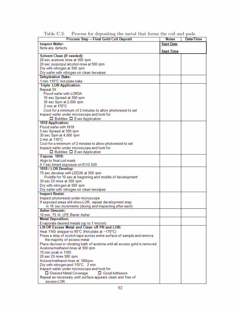
Table C.3: Process for depositing the metal that forms the coil and pads.
92
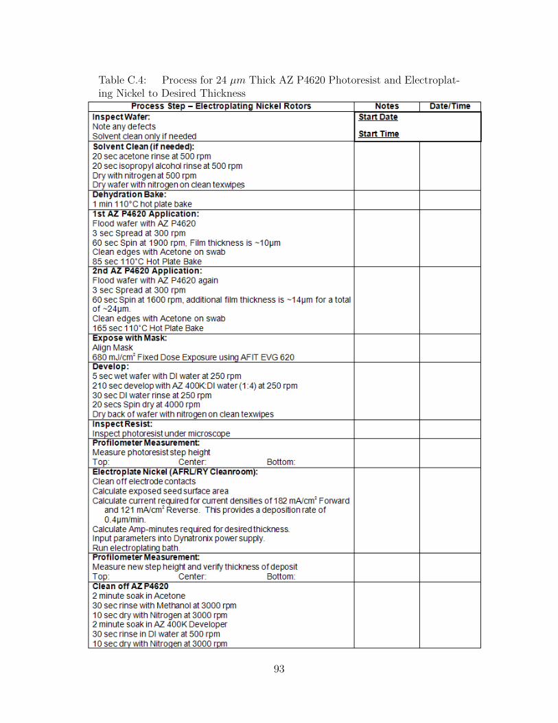
Table C.4: Process for 24 µm Thick AZ P4620 Photoresist and Electroplat-ing Nickel to Desired Thickness
93
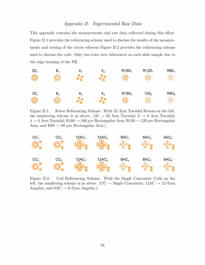
Appendix D. Experimental Raw Data
This appendix contains the measurements and raw data collected during this effort.
Figure D.1 provides the referencing scheme used to discuss the results of the measure-
ments and testing of the rotors whereas Figure D.2 provides the referencing scheme
used to discuss the coils. Only two rows were fabricated on each slide sample due to
the edge beading of the PR.
Figure D.1: Rotor Referencing Scheme. With 32 Arm Toroidal Rotors on the left,the numbering scheme is as above. (32 → 32 Arm Toroidal; 8 → 8 Arm Toroidal;4→ 4 Arm Toroidal; R160→ 160 µm Rectangular Arm; R120→ 120 µm RectangularArm; and R80 → 80 µm Rectangular Arm.)
Figure D.2: Coil Referencing Scheme. With the Single Concentric Coils on theleft, the numbering scheme is as above. (CC → Single Concentric; 12AC → 12-TurnAngular; and 6AC → 6-Turn Angular.)
94

Table D.1: Profilometer Measurements of Rotors. The minimum thickness and themax thickness are presented to illustrate the variations in thickness observed.
95
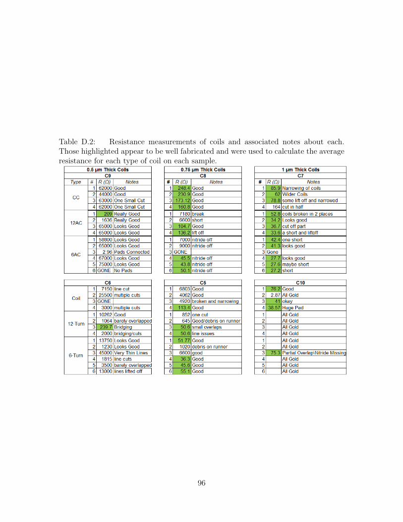
Table D.2: Resistance measurements of coils and associated notes about each.Those highlighted appear to be well fabricated and were used to calculate the averageresistance for each type of coil on each sample.
96
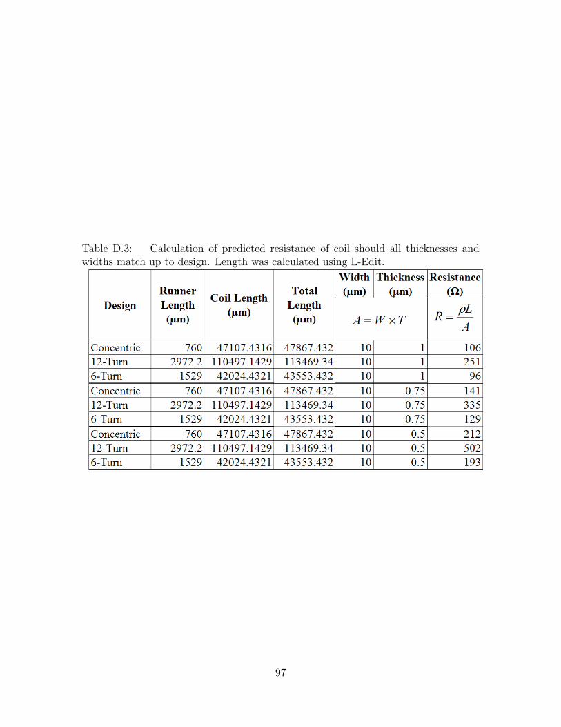
Table D.3: Calculation of predicted resistance of coil should all thicknesses andwidths match up to design. Length was calculated using L-Edit.
97
Bibliography
1. R. C. Johnson, “Energy harvesting matures with growth of wireless sensor net-works,” Electronic Engineering Times, p. 17, December 3 2007.
2. S. Rodgers and J. Sniegowski, “New five-level layering processpioneered by sandia promises more reliable, complex microma-chines.” Sandia National Laboratories, September 1999. Available athttp://www.sandia.gov/media/NewsRel/NR1999/layer.htm.
3. G. T. A. Kovaks, Micromachined Transducers Sourcebook. WCB/McGraw-Hill,1998.
4. K. Fu, A. J. Knobloch, F. C. Martinez, D. C. Walther, C. Fernandz-Pello, A. P.Pisano, D. Liepmann, K. Miyaska, and K. Maurta, “Design and experimentalresults of small-scale rotary engines,” in Proceedings of 2001 ASME InternationalMechanical Engineering Congress and Exposition, November 2001.
5. A. J. Sprecher, “Microfluidic power generation,” Master’s thesis, Air Force Insti-tute of Technology, 2008.
6. I. Buchmann, “Battery university,” February 2007. Available athttp://www.batteryuniversity.com.
7. Anonymous, “The reality behind Moore’s law,” Cyber Aspect, January 2008.Available at http://www.cyber-aspect.com/features/feature article.asp?art=104.
8. Anonymous, “In search of the perfect battery,” The Economist, March 6 2008.Available at http://www.economist.com/displaystory.cfm?story id=10789409.
9. B. S. Lee, P. J. Shih, J. J. He, W. P. Shih, and W. J. Wu, “A study of implantablepower harvesting transducers,” in Proceedings of SPIE - The International Societyfor Optical Engineering, Sensor Systems and Networks: Phenomena, Technology,and Applications for NDE and Health Monitoring, vol. 6530, 2007.
10. C. B. Williams and R. B. Yates, “Analysis of a micro-electric generator for mi-crosystems,” Sensors and Actuators A: Physical, vol. 52, no. 1-3, pp. 8–11, 1996.
11. O. Cugat, “Magnetic micro-actuators and systems (MAGMAS),” IEEE Transac-tions on Magnetics, vol. 39, no. 6, pp. 3607–3612, 2003.
12. D. P. Arnold, “Review of microscale magnetic power generation,” IEEE Trans-actions on Magnetics, vol. 43, no. 11, p. 3940(12), 2007.
13. E. Lefeuvre, A. Badel, C. Richard, L. Petit, and D. Guyomar, “Optimization ofpiezoelectric electrical generators powered by random vibrations,” in Dans Sym-posium on Design, Test, Integration and Packaging (DTIP) of MEMS/MOEMS,2006.
98
14. P. D. Mitcheson, T. C. Green, E. M. Yeatman, and A. S. Holmes, “Architecturesfor vibration-driven micropower generators,” Journal of MicroelectromechanicalSystems, vol. 13, no. 3, pp. 429–440, 2004.
15. B. H. Stark, P. D. Mitcheson, P. Miao, T. C. Green, E. M. Yeatman, and A. S.Holmes, “Converter circuit design, semiconductor device selection and analysis ofparasitics for micropower electrostatic generators,” IEEE Transactions on PowerElectronics, vol. 21, no. 1, pp. 27–37, 2006.
16. G. L. Pollack and D. R. Stump, Electrictromagnetism. Addison Wesley, 2002.
17. P. Kiameh, Electrical Equipment Handbook. McGraw-Hill Higher Education, 2003.
18. P. S. Neelakanta, Handbook of Electromagnetic Materials. CRC Press, 1995.
19. W. Brown, Handbook of Chemistry and Physics. McGraw-Hill, 1958.
20. T. C. Leichle, M. V. Arx, and M. G. Allen, “A micromachined resonant magneticfield sensor,” 14th IEEE International Conference on Micro Electro MechanicalSystems, pp. 274–277, 2001.
21. G. D. Bari, “Nickel plating,” ASM Handbook, vol. 5, 1994.
22. D. R. Lide, ed., CRC Handbook of Chemistry and Physics. CRC Press, 2003.
23. J. Dean, ed., Lange’s Handbook of Chemistry (15th Edition). McGraw-Hill, 1999.
24. G. S. May and S. M. Sze, Fundamentals of Semiconductor Fabrication. JohnWiley and Sons, Inc, 2004.
25. “AZ P4000 Thick Film Photoresist Datasheet.” AZ Electronic Materials, 2005.Available at http://www.az-em.com/PDFs/p4000/az p4000.pdf.
26. A. Ciszewski, S. Posluszny, G. Milczarek, and M. Baraniak, “Effects of saccharinand quaternary ammonium chlorides on the electrodeposition of nickel from awatts-type electrolyte,” Surface and Coatings Technology, vol. 183, pp. 127–133,May 2004.
27. M. Williams, “Electroplating lab notebook.” AFRL/RY Devices Cleanroom,2004.
28. “LOR and PMGI Resist Datasheet.” MicroChem, 2008. Available athttp://www.microchem.com.
29. A. Fitzgerald, C. Kingsley, and S. D. Umans, Electric Machinery - Sixth Edition.McGraw-Hill Handbooks, 2003.
30. Z. Turgut, “Electromagnetics discussion,” January 2007. Air Force ResearchLab/Propulsion Directorate, Wright-Patterson Air Force Base.
99
Vita
James H. Shields was born in Athens, GA in 1979 and raised for the majority
of his youth in Chickamauga, GA. He graduated from Gordon Lee High School in
1997 and began his undergraduate program in Computer Engineering at Brigham
Young University (BYU) in Provo, UT on an Air Force ROTC scholarship that same
year. He put his studies on hold from 1998 to 2000 to serve a two year mission
in northern Argentina for The Church of Jesus Christ of Latter-Day Saints. Upon
returning from his mission, James picked up his studies at BYU and received his
BS in Computer Engineering and a commission into the United States Air Force in
2003. His first assignment was to the Air Force Research Lab, Human Effectiveness
Directorate in Mesa, AZ where he was a program manager and research engineer
for the Intelligence, Surveillance, and Reconnaissance Training Research Group. In
2007 he began his Masters program in Microelectronics and MEMS at the Air Force
Institute of Technology. Upon graduation in March 2009, James will be working
with the Nano/Bio Technology Branch at the Air Force Research Lab, Materials
Directorate.
Permanent address: 2950 Hobson WayAir Force Institute of TechnologyWright-Patterson AFB, OH 45433
100
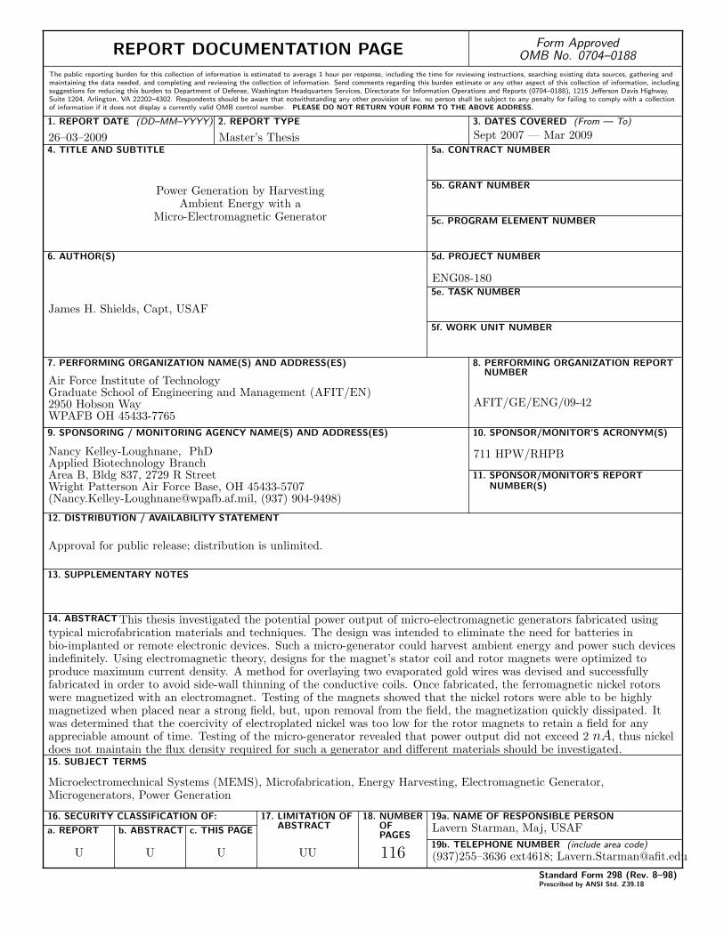
REPORT DOCUMENTATION PAGE Form ApprovedOMB No. 0704–0188
The public reporting burden for this collection of information is estimated to average 1 hour per response, including the time for reviewing instructions, searching existing data sources, gathering andmaintaining the data needed, and completing and reviewing the collection of information. Send comments regarding this burden estimate or any other aspect of this collection of information, includingsuggestions for reducing this burden to Department of Defense, Washington Headquarters Services, Directorate for Information Operations and Reports (0704–0188), 1215 Jefferson Davis Highway,Suite 1204, Arlington, VA 22202–4302. Respondents should be aware that notwithstanding any other provision of law, no person shall be subject to any penalty for failing to comply with a collectionof information if it does not display a currently valid OMB control number. PLEASE DO NOT RETURN YOUR FORM TO THE ABOVE ADDRESS.
1. REPORT DATE (DD–MM–YYYY) 2. REPORT TYPE 3. DATES COVERED (From — To)
4. TITLE AND SUBTITLE 5a. CONTRACT NUMBER
5b. GRANT NUMBER
5c. PROGRAM ELEMENT NUMBER
5d. PROJECT NUMBER
5e. TASK NUMBER
5f. WORK UNIT NUMBER
6. AUTHOR(S)
7. PERFORMING ORGANIZATION NAME(S) AND ADDRESS(ES) 8. PERFORMING ORGANIZATION REPORTNUMBER
9. SPONSORING / MONITORING AGENCY NAME(S) AND ADDRESS(ES) 10. SPONSOR/MONITOR’S ACRONYM(S)
11. SPONSOR/MONITOR’S REPORTNUMBER(S)
12. DISTRIBUTION / AVAILABILITY STATEMENT
13. SUPPLEMENTARY NOTES
14. ABSTRACT
15. SUBJECT TERMS
16. SECURITY CLASSIFICATION OF:
a. REPORT b. ABSTRACT c. THIS PAGE
17. LIMITATION OFABSTRACT
18. NUMBEROFPAGES
19a. NAME OF RESPONSIBLE PERSON
19b. TELEPHONE NUMBER (include area code)
Standard Form 298 (Rev. 8–98)Prescribed by ANSI Std. Z39.18
26–03–2009 Master’s Thesis Sept 2007 — Mar 2009
Power Generation by HarvestingAmbient Energy with a
Micro-Electromagnetic Generator
ENG08-180
James H. Shields, Capt, USAF
Air Force Institute of TechnologyGraduate School of Engineering and Management (AFIT/EN)2950 Hobson WayWPAFB OH 45433-7765
AFIT/GE/ENG/09-42
Nancy Kelley-Loughnane, PhDApplied Biotechnology BranchArea B, Bldg 837, 2729 R StreetWright Patterson Air Force Base, OH 45433-5707([email protected], (937) 904-9498)
711 HPW/RHPB
Approval for public release; distribution is unlimited.
This thesis investigated the potential power output of micro-electromagnetic generators fabricated usingtypical microfabrication materials and techniques. The design was intended to eliminate the need for batteries inbio-implanted or remote electronic devices. Such a micro-generator could harvest ambient energy and power such devicesindefinitely. Using electromagnetic theory, designs for the magnet’s stator coil and rotor magnets were optimized toproduce maximum current density. A method for overlaying two evaporated gold wires was devised and successfullyfabricated in order to avoid side-wall thinning of the conductive coils. Once fabricated, the ferromagnetic nickel rotorswere magnetized with an electromagnet. Testing of the magnets showed that the nickel rotors were able to be highlymagnetized when placed near a strong field, but, upon removal from the field, the magnetization quickly dissipated. Itwas determined that the coercivity of electroplated nickel was too low for the rotor magnets to retain a field for anyappreciable amount of time. Testing of the micro-generator revealed that power output did not exceed 2 nA, thus nickeldoes not maintain the flux density required for such a generator and different materials should be investigated.
Microelectromechnical Systems (MEMS), Microfabrication, Energy Harvesting, Electromagnetic Generator,Microgenerators, Power Generation
U U U UU 116
Lavern Starman, Maj, USAF
(937)255–3636 ext4618; [email protected]