Embed Size (px)
Citation preview

ACTIVE FPGA SECURITY THROUGH DECOY CIRCUITS
THESIS
Bradley D. Christiansen, Major, USAF
AFIT/GE/ENG/06-15
DEPARTMENT OF THE AIR FORCE AIR UNIVERSITY
AIR FORCE INSTITUTE OF TECHNOLOGY
Wright-Patterson Air Force Base, Ohio
APPROVED FOR PUBLIC RELEASE; DISTRIBUTION UNLIMITED

The views expressed in this thesis are those of the author and do not reflect the official
policy or position of the United States Air Force, Department of Defense, or the U.S.
Government.

AFIT/GE/ENG/06-15
ACTIVE FPGA SECURITY THROUGH DECOY CIRCUITS
THESIS
Presented to the Faculty
Department of Electrical and Computer Engineering
Graduate School of Engineering and Management
Air Force Institute of Technology
Air University
Air Education and Training Command
In Partial Fulfillment of the Requirements for the
Degree of Master of Science in Electrical Engineering
Bradley D. Christiansen, Bachelor of Science
Major, USAF
March 2006
APPROVED FOR PUBLIC RELEASE; DISTRIBUTION UNLIMITED

AFIT/GE/ENG/06-15
ACTIVE FPGA SECURITY THROUGH DECOY CIRCUITS
Bradley D. Christiansen, Bachelor of Science
Major, USAF

iv
AFIT/GE/ENG/06-15
Abstract
Field Programmable Gate Arrays (FPGAs) based on Static Random Access
Memory (SRAM) are vulnerable to tampering attacks such as readback and cloning
attacks. Such attacks enable the reverse engineering of the design programmed into an
FPGA. To counter such attacks, measures that protect the design with low performance
penalties should be employed.
This research proposes a method which employs the addition of active decoy
circuits to protect SRAM FPGAs from reverse engineering. The effects of the protection
method on security, execution time, power consumption, and FPGA resource usage are
quantified. The method significantly increases the security of the design with only minor
increases in execution time, power consumption, and resource usage. For the circuits
used to characterize the method, security increased to more than one million times the
original values, while execution time increased to at most 1.2 times, dynamic power
consumption increased to at most two times, and look-up table usage increased to at most
seven times the original values. These are reasonable penalties given the size and
security of the modified circuits. The proposed design protection method also extends to
FPGAs based on other technologies and to Application-Specific Integrated Circuits
(ASICs).
In addition to the design methodology proposed, a new classification of tampering
attacks and countermeasures is presented.

v
Acknowledgments
Whoa! What a ride! At times, the terrain was very rugged. However, “My God
hath been my support; he hath led me through mine afflictions in the wilderness; and he
hath preserved me” (2 Nephi 4:20).
I express my sincere appreciation to my faculty advisor, Dr. Kim. His guidance
and encouragement were keys to the creation of this thesis. Kamsahamnida.
I thank Dr. Baldwin and Dr. Mullins for their review of, and recommendations for
improvement to, this document.
I appreciate the time and effort expended by Mr. Louis Floyd and Mr. Dan
Williams to proofread and comment about drafts of the manuscript.
I am very grateful for the care and concern shown for my family by Mr. Mike
Bristow, Mr. John Duncan, and Mr. Dan Williams during this difficult period. They and
their prayers were a great support to us.
I am eternally grateful to have such a great wife. Her love and belief in me have
carried me through these eighteen months. She has endured more than I during this
period, and her achievements have been greater, especially in the care and development
of our children. She is the primary reason our children greet me with a smile and open
arms. I am grateful to have received the love of my wife and children to remind me of
the truly important treasures of life.
Bradley D. Christiansen

vi
Table of Contents
Page
Abstract .............................................................................................................................. iv
Acknowledgments................................................................................................................v
Table of Contents............................................................................................................... vi
List of Figures ......................................................................................................................x
List of Tables .................................................................................................................... xii
1. Introduction.....................................................................................................................1
1.1 Motivation .............................................................................................................1
1.2 Problem Statement.................................................................................................3
1.3 Research Scope......................................................................................................3
1.4 Research Contributions .........................................................................................4
1.5 Thesis Preview.......................................................................................................4
2. Background......................................................................................................................6
2.1 Chapter Overview..................................................................................................6
2.2 FPGA Defined .......................................................................................................6
2.3 Definition of Terms ...............................................................................................9
2.4 Reverse Engineering Tutorial..............................................................................11
2.5 Attacks.................................................................................................................13
2.6 Protections/Countermeasures ..............................................................................17
2.7 Classification of Attacks and Countermeasures ..................................................20
2.7.1 Introduction .............................................................................................. 20
2.7.2 Previous Works ........................................................................................ 22
2.7.3 Classification of Threats........................................................................... 26

vii
2.7.4 Classification of Countermeasure Security Levels................................... 29
2.8 Related Circuit Protection Research....................................................................31
2.9 Summary..............................................................................................................32
3. Methodology.................................................................................................................33
3.1 Chapter Overview................................................................................................33
3.2 Problem Definition ..............................................................................................33
3.2.1 Goals and Hypotheses .............................................................................. 33
3.2.2 Approach .................................................................................................. 35
3.3 System Boundaries ..............................................................................................38
3.4 System Services...................................................................................................39
3.5 Workload .............................................................................................................41
3.6 Performance Metrics ...........................................................................................41
3.7 Parameters ...........................................................................................................42
3.7.1 System ...................................................................................................... 42
3.7.2 Workload .................................................................................................. 42
3.8 Factors .................................................................................................................43
3.9 Evaluation Technique..........................................................................................45
3.10 Experimental Design .........................................................................................46
3.11 Analyze and Interpret Results ...........................................................................47
3.12 Summary............................................................................................................47
4. Design Algorithm..........................................................................................................49
4.1 Chapter Overview................................................................................................49
4.2 Combination Lock ...............................................................................................49

viii
4.3 Decoy Circuit Generation from Truth and State Tables......................................52
4.3.1 Combinational Circuit .............................................................................. 54
4.3.2 Sequential Circuit ..................................................................................... 63
4.4 Decoy Circuit Generation from Boolean Equations............................................66
4.5 Decoy Circuit Generation from Gate-level Representation ................................69
4.6 Decoy Circuit Generation from Existing VHDL.................................................72
4.7 Decoy Circuit Generation through Partial Scrambling .......................................77
4.8 Summary..............................................................................................................84
5. Results and Analysis .....................................................................................................87
5.1 Chapter Overview................................................................................................87
5.2 Security................................................................................................................87
5.2.1 Combination Lock .................................................................................... 91
5.2.2 Combinational Circuit .............................................................................. 92
5.2.3 Sequential Circuit ..................................................................................... 93
5.2.4 VHDL and Partial Scrambling ................................................................. 97
5.3 Execution Time ...................................................................................................98
5.3.1 Combination Lock .................................................................................... 98
5.3.2 Combinational Circuit .............................................................................. 99
5.3.3 Sequential Circuit ................................................................................... 101
5.3.4 VHDL and Partial Scrambling ............................................................... 101
5.4 Power Consumption ..........................................................................................102
5.4.1 Combination Lock .................................................................................. 103
5.4.2 Combinational Circuit ............................................................................ 105

ix
5.4.3 Sequential Circuit ................................................................................... 107
5.4.4 VHDL and Partial Scrambling ............................................................... 109
5.4.5 Observations ........................................................................................... 109
5.5 Resource Usage .................................................................................................110
5.5.1 Combination Lock .................................................................................. 111
5.5.2 Combinational Circuit ............................................................................ 111
5.5.3 Sequential Circuit ................................................................................... 115
5.5.4 VHDL and Partial Scrambling ............................................................... 117
5.6 Combining a Combination Lock with Modified Circuits..................................117
5.7 Summary............................................................................................................119
6. Conclusions and Recommendations ...........................................................................121
6.1 Chapter Overview..............................................................................................121
6.2 Conclusions of Research ...................................................................................121
6.3 Significance of Research ...................................................................................122
6.4 Recommendations for Action............................................................................122
6.5 Recommendations for Future Research.............................................................123
6.6 Summary............................................................................................................124
Appendix: Data Analysis Tables ....................................................................................125
Bibliography ....................................................................................................................136
Vita ..................................................................................................................................141

x
List of Figures
Figure Page
1. Downed F-117A. ......................................................................................................... 1
2. Captured EP-3E. .......................................................................................................... 2
3. Altera Stratix Logic Element. ...................................................................................... 7
4. Generalized FPGA interconnect. ................................................................................. 8
5. Cross sections of unprogrammed and programmed antifuses. .................................... 8
6. FPGA with SRAM switches........................................................................................ 9
7. Black Box attack........................................................................................................ 14
8. Cloning attack............................................................................................................ 14
9. Power consumption plot of DES implementation. .................................................... 15
10. Reverse engineering an ASIC.................................................................................... 16
11. Use of an encrypted configuration file. ..................................................................... 19
12. On-FPGA PROM....................................................................................................... 19
13. Rearranging design modules...................................................................................... 20
14. Matrix classification. ................................................................................................. 27
15. Methodology design flow. ......................................................................................... 36
16. System and component under test. ............................................................................ 38
17. Eight-state Combination Lock. .................................................................................. 53
18. Full adder schematic. ................................................................................................. 55
19. Modified full adder schematic. .................................................................................. 62
20. Three-bit up counter schematic. ................................................................................ 63

xi
Figure Page
21. Page 3 of 4 of the modified counter schematic.......................................................... 67
22. Original gate-level representation.............................................................................. 70
23. Modified gate-level representation. ........................................................................... 71
24. Four-bit priority encoder schematic........................................................................... 74
25. Modified four-bit priority encoder schematic............................................................ 78
26. Schematic of result=a*b+c. ...................................................................................... 79
27. Page 1 of partial scrambling schematic. .................................................................... 85
28. Page 2 of partial scrambling schematic. .................................................................... 86
29. Security vs. varying extra inputs. .............................................................................. 89
30. Security vs. varying copies. ....................................................................................... 89
31. Security vs. varying extra outputs. ............................................................................ 90
32. Quartus II PowerPlay Power Analyzer Tool. .......................................................... 103
33. Combinational circuits’ static power consumption. ................................................ 106
34. Correlation between pin count and static power...................................................... 110
35. Combinational circuits’ LUT increase for circuits 1-4............................................ 112
36. Combinational circuits’ LUT increase for circuits 5-8............................................ 113
37. Combinational circuits’ pin increase. ...................................................................... 114

xii
List of Tables
Table Page
1. Attacks and countermeasures. ................................................................................... 21
2. IBM security level scheme. ....................................................................................... 23
3. Design steps and attacks they counter. ...................................................................... 38
4. Failure mode combinations........................................................................................ 40
5. Full adder truth table.................................................................................................. 54
6. Expanded full adder truth table.................................................................................. 55
7. Expanded full adder truth table with complete top half. ........................................... 57
8. Final expanded full adder truth table. ........................................................................ 57
9. Three-bit up counter state table. ................................................................................ 63
10. Copies 1 and 2 of modified counter........................................................................... 64
11. Copies 3 and 4 of modified counter........................................................................... 65
12. Resulting truth table from Boolean equation modification. ...................................... 68
13. Resulting state table from gate-level modification. ................................................... 72
14. Priority encoder truth table. ....................................................................................... 73
15. Resulting truth table for partial scrambling. .............................................................. 80
16. Combinational multiplexer input and output combinations. ..................................... 80
17. Combination Locks’ security contributions............................................................... 91
18. Analysis of Combination Locks’ security contributions. .......................................... 92
19. Combinational circuits’ security metrics. .................................................................. 93
20. Analysis of combinational circuits’ security contributions. ...................................... 94

xiii
Table Page
21. Sequential circuits’ security metrics. ......................................................................... 95
22. Analysis of sequential circuits’ security contributions. ............................................. 96
23. Original and scrambled existing VHDL circuits’ security. ....................................... 97
24. Security metrics of original and partially scrambled circuits. ................................... 98
25. Combination Locks’ maximum clock frequencies. ................................................... 98
26. Results of Combination Locks’ maximum frequency analysis table. ....................... 99
27. Combinational circuits’ execution times. ................................................................ 100
28. Results of combinational circuits’ execution time analysis table. ........................... 101
29. Existing VHDL designs’ execution times. .............................................................. 101
30. Partially scrambled and original circuits’ execution times...................................... 102
31. Combination Locks’ power consumption................................................................ 103
32. Results of Combination Locks’ static power analysis table. ................................... 104
33. Results of Combination Locks’ dynamic power analysis table............................... 104
34. Combinational circuits’ power consumption........................................................... 105
35. Results of combinational circuits’ static power analysis table. ............................... 107
36. Results of combinational circuits’ dynamic power analysis table........................... 107
37. Sequential circuits’ power consumption.................................................................. 108
38. Results of sequential circuits’ static power analysis table....................................... 108
39. Results of sequential circuits’ dynamic power analysis table. ................................ 108
40. VHDL circuits’ power consumption. ...................................................................... 109
41. Partially scrambled circuits’ power consumption.................................................... 109

xiv
Table Page
42. Combination Locks’ resource usage........................................................................ 111
43. Results of Combination Locks’ LUT analysis table................................................ 111
44. Combinational circuits’ resource usage................................................................... 112
45. Results of combinational circuits’ LUT analysis table............................................ 114
46. Results of combinational circuits’ pin analysis table. ............................................. 115
47. Sequential circuits’ resource usage.......................................................................... 115
48. Results of sequential circuits’ LUT analysis table. ................................................. 116
49. Results of sequential circuits’ pin analysis table. .................................................... 117
50. VHDL circuits’ resource usage. .............................................................................. 117
51. Partially scrambled circuits’ resource usage............................................................ 117
52. Combination Lock and modified full adder............................................................. 118
53. Combination Lock and modified counter. ............................................................... 118
54. Combination Lock and modified VHDL circuit...................................................... 118
55. Analysis of Combination Locks’ maximum frequencies. ....................................... 125
56. Analysis of Combination Locks’ static power consumptions. ................................ 125
57. Analysis of Combination Locks’ dynamic power consumptions. ........................... 126
58. Analysis of Combination Locks’ LUT usages......................................................... 126
59. Analysis of combinational circuits’ execution times............................................... 127
60. Analysis of combinational circuits’ static power consumptions. ............................ 128
61. Analysis of combinational circuits’ dynamic power consumptions. ....................... 129
62. Analysis of combinational circuits’ LUT usages..................................................... 130

xv
Table Page
63. Analysis of combinational circuits’ pin usages. ...................................................... 131
64. Analysis of sequential circuits’ static power consumptions. ................................... 132
65. Analysis of sequential circuits’ dynamic power consumptions............................... 133
66. Analysis of sequential circuits’ LUT usages. .......................................................... 134
67. Analysis of sequential circuits’ pin usages. ............................................................. 135

1
ACTIVE FPGA SECURITY THROUGH DECOY CIRCUITS
1. Introduction
1.1 Motivation
As an F-117A Nighthawk stealth fighter made its way to its target on 27 March
1999 [FAS00], enemy forces pieced together its flight path, from takeoff to the target
area. Using knowledge from previous Nighthawk strikes, possible returns from low-
frequency radars, and the hint from a dropped bomb, the enemy was able to down the
aircraft with a surface-to-air missile (cf., Figure 1). Fortunately, the pilot safely ejected
and was rescued before being captured. The decision had to be made whether to destroy
the remains of the plane to protect its stealth technology [Lam02] and the specialized
circuits used in the flight control system.
Figure 1. Downed F-117A. Note the HO designation for Holloman AFB, NM, home of the F-117As. [FAS00]

2
Almost two years later, as a U.S. Navy EP-3E Aires II surveillance aircraft was
conducting a routine mission in international airspace, a Chinese fighter bumped the
EP-3E’s wing, necessitating an emergency landing in Chinese territory (cf., Figure 2)
[New01]. Although the crew was trained to destroy sensitive equipment in the event of
capture [DoD01], the equipment may not have been sufficiently destroyed before landing
to preclude Chinese exploitation. Among the systems that might have been exploited by
the Chinese was the Link-11 secure communications system [Smi01]. It is also possible
that classified circuits were also compromised.
Figure 2. Captured EP-3E. Note the chipped propeller blade at (2) and the missing radome at (3). [Tri01]
The above examples illustrate the need to protect critical technologies in military
systems. The United States Air Force goes to great lengths to maintain technological
superiority, avoid technological surprise, and achieve a return on investment from
advanced technology development. Protecting integrated circuit designs found in
weapons systems helps to achieve those goals [AFR05]. Such protection enables a
weapon system to have a long life without compromising its capabilities. Additionally, a
protected design can prevent an adversary from increasing his knowledge base and
advancing his technology [HuS99].

3
Field-programmable gate arrays (FPGAs) are increasingly taking the place of
application-specific integrated circuits (ASICs) due to their flexibility, increasing
densities [Act02], and lower non-recurring engineering costs. Reprogrammable FPGAs
are attractive for applications with requirements that change over time, where changes
need to be implemented quickly, or for quickly fielding a new product. As more
commercial systems are designed with FPGAs rather than ASICs, an increasing number
of military systems will also contain FPGAs.
FPGAs have some intrinsic vulnerabilities, including the possibility of extracting
the circuit design through reverse engineering [AFR05]. In the corporate arena,
protecting a design on an FPGA from reverse engineering helps maintain a competitive
edge, market share, and revenues. Securing a design in a military application maintains
its technological advantage, prevents the exploitation of a design by an adversary, and
consequently can save lives.
1.2 Problem Statement
The challenge, then, is to devise methods of protecting designs on FPGAs that
completely eliminate reverse engineering vulnerabilities or, at a minimum, introduce
delays that make reverse engineering impractical. A worthwhile new design protection
method balances increased security against increased implementation costs, decreased
system performance, and increased operations and maintenance costs [AFR05].
1.3 Research Scope
The purpose of this research is to devise a method to secure integrated circuit
designs implemented in FPGAs and then evaluate its effectiveness. A novel process is

4
proposed to protect designs specified using truth or state tables, with Boolean equations
or that are already implemented in VHDL (Very high-speed integrated circuit Hardware
Description Language). The proposed design methodology will produce secure
application-specific integrated circuits, as well as secure FPGA designs. This procedure
is demonstrated using several common circuits. The power consumption, execution
times, and resource usage of the original and modified circuits are measured and
compared.
1.4 Research Contributions
This research proposes a new attack classification scheme that combines of cost
and time. A countermeasure classification system easily correlated to the attack
classification is also developed.
In addition, the research contributes an innovative technique that provides
significant protection to FPGA and ASIC designs against reverse engineering. The
performance penalty to apply this technique to FPGA designs are only minor increases in
execution time and power consumption. Increased resource requirements can be
accommodated with the generally available excess FPGA resources.
The design methodology is demonstrated using circuits described in various ways
from Boolean equations to VHDL. Additionally, the flexibility of the algorithm to
modify only a portion of a circuit is illustrated.
1.5 Thesis Preview
Chapter 2 provides background information on FPGAs and reverse engineering,
gives definitions, lists and classifies attacks and countermeasures, and presents relevant

5
existing research. Chapter 3 describes the testing methodology and provides an overview
of the proposed circuit modification process. Chapter 4 gives the details of the proposed
design methodology by illustrating it with several examples. Chapter 5 presents the test
results and analyses. Chapter 6 presents a summary, explains the significance of the
research, and makes recommendations for further study.

6
2. Background
2.1 Chapter Overview
The purpose of this chapter is to provide sufficient background for the reader to
understand the context of the research. After covering FPGA architectures, the terms
tampering and reverse engineering are defined, followed by a brief tutorial about reverse
engineering. Finally, FPGA design threats and possible countermeasures to these threats
are presented, as well as a threat and countermeasure classification scheme.
2.2 FPGA Defined
A field-programmable gate array (FPGA) is a computer chip that a user can
program in the field to accomplish a particular function. For example, a user could
program an FPGA to be a general purpose microprocessor or to encrypt or decrypt data.
FPGAs are generally divided into cells called configurable logic blocks (CLBs), which
may contain the following:
• look-up tables (LUTs) to accomplish logic functions, such as
Y = (B AND D) XOR C,
• arithmetic logic gates to implement other logic functions or to combine
outputs from LUTs,
• multiplexers to select particular outputs, and
• storage elements (memory) such as D flip-flops.
Figure 3 shows a portion of a CLB. CLBs are interconnected with wires that can be

7
Figure 3. Altera Stratix Logic Element. This is one tenth of a Logic Array Block (Altera's nomenclature for a CLB). [Alt05] programmed to provide specific paths between CLBs or to input or output pins as shown
in Figure 4 [BrR96, Xil05].
Programmable elements are controlled by switches that determine the function of
that building block. The switches are generally either antifuses or SRAM (static random
access memory) elements. An antifuse is a ‘sandwich’ configuration consisting of an
insulator between two conductors. The insulator electrically isolates the conductors when
the antifuse is not programmed. When the antifuse is programmed by applying a voltage,
the insulator provides a low-resistance path between the conductors. Figure 5 shows an
unprogrammed antifuse (a) and a programmed antifuse (b). The boxed area of (b) shows
where the connection between the two conductors has been made. Antifuse FPGAs are

8
Figure 4. Generalized FPGA interconnect. Adapted from [BrR96].
Figure 5. Cross sections of unprogrammed and programmed antifuses. [Act06]
one-time-programmable, while SRAM FPGAs are reprogrammable. The appropriate
value to either activate or deactivate a particular path or function is stored in an SRAM
element. Figure 6 shows SRAM switches configured to connect two logic blocks through
two interconnections and a multiplexer. An SRAM element loses its programming
(theoretically) when power is disconnected. To program an FPGA, a configuration file
(also called a bit stream) is usually created in a software application. This configuration

9
Figure 6. FPGA with SRAM switches. [BrR96]
file is downloaded directly to the FPGA or to a memory device (flash memory or a
PROM – programmable read-only memory). The memory stores the configuration file
and programs an SRAM-based FPGA at start-up since the SRAM switches lose their
state after a loss of power. The bits in the configuration file dictate the switch settings
[BrR96, WGP04].
2.3 Definition of Terms
It is important to understand the definitions of the following terms as they are
used in this research.
Tampering is defined as activities that secretly, dishonestly, or interfere or intrude
without consent [Pri05]. Such activities, accomplished through direct physical or remote
electronic access, include destruction, modification, observation, and theft of integrated
circuits [IEEE93]. The theft could be of the entire chip for use in another system or of

10
the design for duplication and distribution. The entire circuit, or just a portion thereof,
could be destroyed, modified, or observed. The observation of a circuit, possibly in
conjunction with modifications, could reveal private information or proprietary
algorithms, technologies, or processes.
As the following examples show, tampering has varying levels of difficulty and
complexity.
• If physical access is achieved, an entire chip could be stolen, or, with more
effort, the circuit design itself could be stolen.
• Modifying an ASIC directly may be more difficult than remotely
modifying a reprogrammable FPGA.
• The entire chip could be destroyed or, with more sophisticated tools, a
specific area of the chip could be targeted for destruction.
• The leads of a chip could be probed or, at an increased level of
complexity, the signals within a circuit could be observed.
Reverse Engineering, a subset of tampering, is defined as methods, processes, and
analyses used to recreate a design from a final product [Ang06] or other process outputs
[Geo05], to create a “representation at a higher level of abstraction” [J-STD95], or to
determine the technology that is used [Geo05].
In general, reverse engineering requires more effort and resources than tampering
alone. For example, deciphering a secret key in a cryptographic system is tampering, but
discovering how the algorithm is implemented would be reverse engineering. Likewise,
obtaining an unencrypted FPGA configuration file and using it to program other FPGAs

11
would be tampering, while deciphering the configuration file would be reverse
engineering. Tampering to observe an integrated circuit is a prerequisite for analyses that
would use the observations to recreate the design.
Being a subset of tampering, reverse engineering also occurs at varying levels. At
one level, a cryptographic implementation may be discovered. At another level, the
fabrication processes and technology used in that implementation might be determined.
Thus, a secure FPGA design would prevent interference with its operation,
intrusion into its functionality, its replication, and the determination of its fundamental
technology.
Anti-Tampering and Anti-Reverse Engineering are actions taken to hinder or
prevent tampering and reverse engineering.
2.4 Reverse Engineering Tutorial
Since the goal of the proposed design methodology is to produce an FPGA design
resistant to reverse engineering, it is appropriate to review the stages of a reverse
engineering process. The following list of stages, which apply specifically to ASICs, is
excerpted from [CEL99]. Following this list of stages, the application of these stages to
FPGAs is discussed.
According to [CEL99], the following stages of the reverse engineering process
were identified at the Argonne National Laboratory’s 1998 Reverse Engineering
Workshop.
1. Sample preparation: An ASIC must be cross-sectioned or chemically
etched to reveal its internal construction. Since this step is destructive,

12
great care must be taken to avoid damaging the components of interest.
Several samples may be required, as well as several iterations of slicing or
etching subsequent layers and the next stage [AnK96].
2. Image acquisition: Once the internal construction is revealed, it must be
imaged, section by section. The images of the sections are pieced together
for a complete image. A scanning electron microscope may be required,
depending on the size of the transistors.
3. Geometric description: Geometric data is extracted from the image file
and converted to a geometric data stream. Information about the
technology employed to realize the circuit is necessary for the conversion
of the image to geometric data.
4. Transistor netlist: From the geometric data, transistors are identified
through design-rule checkers.
5. Gate-level netlist: Specific gates are identified from collections of
transistors. For example, AND or NOR gates may be identified. Since
gates generally have the same geometry, pattern-matching enables the
process to be automated.
6. Module-level description: With the gates identified, modules such as
multiplexers and full adders can be abstracted.
7. Register-transfer and behavioral descriptions: Further abstraction
generates a register-transfer-level representation and eventually a

13
behavioral description. (In 1999, the technology to produce these
interpretations was not available.)
Reverse engineering an FPGA design uses stages similar to those listed above. If
the FPGA is antifuse-based, it has to be cross-sectioned and imaged. For an SRAM-
based FPGA, sample preparation and image acquisition determine the contents of the
SRAM elements that act as switches. (The process of discovering the state of an SRAM
is discussed further in Section 2.5.) The processes of generating a geometric description
and a transistor netlist are equivalent to correlating each switch with an FPGA
interconnect intersection or CLB element. With that correlation information, gates and
modules can be composed.
An FPGA can also be reverse engineered from its unencrypted configuration file.
In such a case, obtaining the FPGA bit stream is equivalent to the sample preparation
stage for an ASIC. A correlation similar to the one above is done between the bits of the
file and entities on the FPGA, and the process continues with the reconstruction of gates
and modules.
2.5 Attacks
Partly due to its flexibility and its programming method, an FPGA is vulnerable to
reverse engineering (i.e., the determination of the implemented circuit design). Various
methods can derive the functionality of a programmed FPGA. These methods include
[WGP04]:
a. Black Box Attacks: All possible inputs are applied and the outputs are
observed as illustrated in Figure 7.

14
Figure 7. Black Box attack.
b. Readback Attacks: The FPGA’s configuration data is read directly from
the FPGA.
c. Cloning Attacks: An attacker eavesdrops on the transmission of the
configuration file from memory to the FPGA and uses the stolen file to program a clone
FPGA as shown in Figure 8.
Figure 8. Cloning attack.
d. Reverse-Engineering an unencrypted configuration: This is done after
attack (b) or (c) above.
e. Side-Channel Attacks: These attacks include power consumption
analysis, timing analysis, electromagnetic (EM) radiation analysis, and injecting faults to
reveal functionality. Figure 9 shows the power consumption plot of a Data Encryption
Standard implementation, which clearly shows 16 rounds of the algorithm.
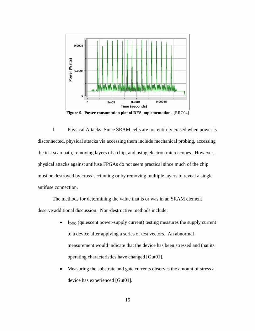
15
Figure 9. Power consumption plot of DES implementation. [RRC04]
f. Physical Attacks: Since SRAM cells are not entirely erased when power is
disconnected, physical attacks via accessing them include mechanical probing, accessing
the test scan path, removing layers of a chip, and using electron microscopes. However,
physical attacks against antifuse FPGAs do not seem practical since much of the chip
must be destroyed by cross-sectioning or by removing multiple layers to reveal a single
antifuse connection.
The methods for determining the value that is or was in an SRAM element
deserve additional discussion. Non-destructive methods include:
• IDDQ (quiescent power-supply current) testing measures the supply current
to a device after applying a series of test vectors. An abnormal
measurement would indicate that the device has been stressed and that its
operating characteristics have changed [Gut01].
• Measuring the substrate and gate currents observes the amount of stress a
device has experienced [Gut01].

16
• Using the circuitry intended for device testing, such as JTAG boundary
scan [Gut01].
• Voltage contrast imaging detects logic levels and voltages through the
examination of the differences in the brightness of the voltage intensity
image [SoA93].
One invasive technique uses a focused ion beam (FIB) workstation to drill minute access
holes for probing deeply buried entities. The FIB workstation can also inject metal probe
points for easier device examination [Gut01]. Although the literature does not describe
the use of these methods of attack against SRAM FPGAs, it is conceivable that they
could be used to determine the programming of such a device [WGP04].
The attacks that could also be used against ASICs include black box, side-
channel, and physical attacks [RRC04]. For example, with the destruction of only six
chips, an Intel 80386 was reverse engineered in two weeks using the specific physical
attack described in the Reverse Engineering Tutorial section above [AnK96]. Figure 10
illustrates the third stage in the reverse engineering process, where an integrated circuit
image is converted to a geometric data format such as Graphic Design Station II (GDSII).
Figure 10. Reverse engineering an ASIC. [ACA02]

17
2.6 Protections/Countermeasures
There are various approaches to protect a design on an FPGA or to mitigate the
effects of its theft and reproduction. Policy and law protections such as patents and
copyrights allow private companies to sue an alleged thief for damages. To aid in
proving ownership in the event a design is stolen, the original producer might embed a
watermark in the design [JYP03]. Export control laws attempt to maintain a nation’s
technological advantage. Security classifications and laws that prescribe punishments for
espionage and treason also attempt to protect a nation’s technological capital. If
classified knowledge is compromised, a non-disclosure agreement (NDA), which is
generally executed to obtain a security clearance, may have been breached. NDAs are
also signed before a manufacturer grants access to its FPGA bit stream design [WGP04]
or to the mapping between switches and function elements.
If these policy protections are subverted, months or years could elapse before a
theft is discovered, by which time significant damage may have already been done. Such
was the case with atomic bomb secrets stolen from Los Alamos and given to the Soviet
Union [FBI06]. In the corporate arena, by the time such a theft is discovered, a
company’s market share may have already been lost to a company in a foreign nation that
not only refuses to enforce patents but also encourages such piracy. Likewise, a
disgruntled former employee of Company X could begin employment with Company Y
and describe how a watermark might be removed from a design stolen from Company X.
With these subversions, stronger protections are warranted for high-value assets.
Encryption has long been utilized to protect messages. However, even encryption

18
algorithms will eventually be cracked as was the case of the Data Encryption Standard
[EFF98]. As described in FIPS 140-2, there are also physical protections such as
containers, tamper-evident coatings, and circuitry that detects and responds to
unauthorized access [NIS02]. One example of a FIPS 140-2 Security Level 4 device is
the IBM 4758 PCI Cryptographic Coprocessor [IBM06]. The circuitry of this device is
surrounded by a mesh that detects physical penetrations and abnormal environmental
conditions in parameters such as temperature and radiation. The response to such an
attack is the erasure of critical secret data.
There are countermeasures stronger than policy that can protect the design of a
circuit programmed into an FPGA. These include [WGP04]:
a. The complexity of state-of-the-art FPGAs, which mitigates a black box
attack.
b. A security bit can prevent a readback attack. However, it is possible that
fault injection may defeat this countermeasure. Applying unusual voltages or voltage
transients could reset the security bit [AnK96]. If fault injection is a possibility, the
FPGA should be placed in a secure environment.
c. Encrypting, as in Figure 11, and/or storing the configuration file in
memory resident on the FPGA, as in Figure 12, can prevent cloning attacks. Encryption
also prevents reverse engineering a file. (The devices described in [Xil05], however, can
decrypt an encrypted configuration file.)

19
Figure 11. Use of an encrypted configuration file. Adapted from [Kea01].
Figure 12. On-FPGA PROM.
d. Techniques to prevent side-channel attacks include inserting random
values to mask secret information, smoothing power traces, and changing logic at the
transistor level.
e. To prevent physical attacks on SRAM FPGAs, memory retention should
be reduced as much as possible through methods such as periodically inverting the bits,
applying an opposite current, inserting dummy cycles, or rearranging the data using
dynamically reconfigurable FPGAs as in Figure 13.

20
Figure 13. Rearranging design modules.
Table 1 summarizes the attacks and countermeasures discussed above Though
the attacks and countermeasures listed are not necessarily specific to FPGA designs,
some of the methods have been used against or on underlying FPGA technologies, such
as SRAM. Attacks and countermeasures with respect to embedded systems have also
been examined [RRC04].
2.7 Classification of Attacks and Countermeasures
2.7.1 Introduction
An attacker who tampers with an integrated circuit can harm both the developer
and the user of the circuit. If the effects of tampering are widespread, the developer is
damaged by a reputation for circuit malfunctions. Furthermore, revenue could be lost if
the design is copied and distributed, since the developer does not recoup the research and
development costs. Likewise, the user may be denied service due to destructive
tampering of a circuit or lose information that was supposedly secure due to observation
of a circuit. In security and defense applications, lives could be lost due to tampering or
reverse engineering. A tampering attack could result in a malfunction that causes a

21
Table 1. Attacks and countermeasures. [WGP04]
Attack Used against FPGAs?
Countermeasure Available in commercial
FPGAs? Black Box Yes Inherent FPGA size and
design complexity Yes
Readback (Security bit possibly overcome with fault injection)
Yes (Not specifically)
Employ a security bit (Secure environment) See 1 and 2 below
Yes (User-specific) See 1 and 2 below
Cloning Yes Reverse-Engineer the configuration file
Yes 1. Encrypt the configuration file 2. Store the configuration file in FPGA
1. Yes 2. Varies
Physical Little specifically published
Reduce the memory-retention effects
Not specifically
Side-Channel Yes A. Insert random values B. Smooth the power traces C. Change the logic
Not specifically
vehicle to crash or the loss of the designed technological advantage of a weapon or
countermeasure.
Countermeasures are employed to thwart such tampering attacks. These methods
vary in cost and effectiveness. Thus, an understandable classification is needed to apply
appropriate protection mechanisms against perceived threats. However, there are no
universally accepted classifications of threats and protection levels for integrated circuits.
In fact, there is no IEEE standard that addresses either of these classifications. This
section presents a classification of tampering threats and a corresponding classification of
protection levels.

22
In [ADD91], Abraham et al. propose a classification of attackers based on the
attacker’s knowledge and available resources. They also present a security level scheme
that appears to be loosely correlated with the attacker classification. Anderson and Kuhn
apply the attacker classification to specific attack examples in [AnK96] and [AnK97].
Actel Corporation in [Act02] also references [ADD91] to compare the security offered by
their FPGAs to that offered by other manufacturers’ devices.
The following subsection explains the IBM classifications and describes the usage
of these classifications in other applications. Threats against ASICs and FPGAs are also
presented and classified. Examples of countermeasures are given, along with a security
level classification correlated to the threat classification. Alternate classifications based
on the time required to crack a design are also given.
2.7.2 Previous Works
To define the potential physical threats against the Transaction Security System,
attackers are categorized as [ADD91]:
Class I (clever outsiders)—They are often very intelligent but may have insufficient knowledge of the system. They may have access to only moderately sophisticated equipment. They often try to take advantage of an existing weakness in the system, rather than try to create one. Class II (knowledgeable insiders)—They have substantial specialized technical education and experience. They have varying degrees of understanding of parts of the system but potential access to most of it. They often have access to highly sophisticated tools and instruments for analysis. Class III (funded organizations)—They are able to assemble teams of specialists with related and complementary skills backed by great funding resources. They are capable of in-depth analysis of the system, designing sophisticated attacks, and using the most sophisticated analysis tools. They may use Class II adversaries as part of the attack team.

23
Security levels which correlate to the resources (time, money, knowledge) required to
conduct an attack on a system are also defined. Table 2 summarizes their security levels.
Table 2. IBM security level scheme. Adapted from [ADD91].
Definition Security
Level Knowledge/Skills Tools/Equipment Tool or
Total Cost Notes ZERO —— —— —— No special
security features LOW —— Common lab or
shop tools —— Some security features
MODL Some specialized knowledge
More expensive $500 - $5,000 (tools) ——
MOD Some special skills and knowledge
Special tools and equipment
$5,000 - $50,000 (tools)
Attack time-consuming, but successful
MODH Special skills and knowledge; adversarial team effort
Available, but expensive to buy and operate
$50,000 - $200,000 or more
Attack could be unsuccessful
HIGH Team of specialists
Highly specialized, which may have to be built
$1,000,000 or more
Known attacks unsuccessful; attack success in question
Even though both an attacker classification and a protection level scheme are
defined, the correlation between the two is not clear. It appears that the LOW security
level corresponds to a Class I attacker, the MOD security level could correspond to a
Class II attacker, and the HIGH security level corresponds to a Class III attacker. In
addition, the security levels MODL and MODH do not clearly fall between the outsiders
of Class I and the insiders of Class II and between the insiders of Class II and the funded
organizations of Class III, respectively. Thus, how is an outsider classified who is more
than clever but less than a funded organization?

24
The IBM attacker categorization has been used to classify several example attacks
[Ank96]. The IBM scheme defines Class I as the application of low and high voltages,
and power and clock transients, which can be applied non-invasively. For example,
directing UV light at the security lock cell of an EPROM, or removing a smartcard chip
with a knife, nitric fuming acid, and acetone are Class I attacks. A Class II attack
removes each chip layer, imaging it using the Schottky effect and an electron beam, and
reconstructing the collection of images with image processing software. Another Class II
attack uses a focused ion beam (FIB) workstation to actively attack a chip. Although the
use of the FIB workstation is considered Class II, a Class I attacker could rent time on
such machines. A Class III attacker is one whose resources are such that “chip contents
cannot be kept from” the attacker [AnK96].
Class distinctions do not hold when an attacker can access equipment available
predominantly to an attacker of a higher class. For example, a Class I attacker can rent
time on a FIB workstation, a tool predominantly available to a Class II attacker.
Furthermore, the insider threat is not considered, and Class II is also applied to academics
who apparently have no privileged information.
Actel Corporation references [ADD91] in [Act02], but it is not entirely clear
whether the reference is to IBM’s attacker classification or security level scheme. Actel
definitions of security levels are close, though not exact, restatements of IBM’s security
level definitions. However, Actel uses numbers and + or - for the security levels rather
than names as IBM did. In addition, the words “Class” and “Level” are interchanged.
With this modification of IBM’s attacker classification and/or security level scheme,

25
Actel claims that conventional SRAM FPGAs are Class or Level 1, SRAM FPGAs with
DES encryption are Level 2, and Actel products are Level 2+. A Level 3 example is not
given, and the insider threat is not addressed.
[ETS05] applies the IBM classification to attackers of bus encryption hardware.
The classification is presented in the context of smartcard memories but was used only
sparingly [NPS03]. Others assert the IBM classification should not be used to describe
the tamper-proof level of wireless sensor networks, but rather, the level should be defined
in terms of network availability [PaS05].
Attacks have also been categorized using privacy, integrity, or availability attacks
[RRC04]. Another classification divides attacks among physical, side-channel, and
software attacks. Countermeasures are presented and correlated with the second attack
classification, but they are not classified with a security level [RRC04].
These previous classifications have obstacles to their understandability and use.
Classifying the insider threat, as well as the outsider with moderate resources but no
private information, has been a challenge. Also problematic has been the distinction
between classes when a member of one class has access to tools of another class. If both
attack/attacker classification and countermeasure security level classification are given,
the correlation between them is generally absent. The attacker classification is often used
to determine a security level. Whatever the obstacles, there are not universally accepted
classifications of threats and countermeasure security levels and a correlation between the
two.

26
2.7.3 Classification of Threats
To overcome the shortfalls of the previous classifications, the following matrix
categorization is proposed. This categorization uses the attacks, not attackers, based on
the resources and time required to successfully accomplish the attack. In this way, the
dissolution of classes does not occur when a member of one class uses tools of another.
The proposed classification also accounts for the insider threat and the outsider with
moderate resources but no inside knowledge. Finally, a correlation can easily be made to
protection levels, as discussed in the next subsection.
It is appropriate to classify the attacks and not the attackers. For example, a
bullet-proof vest should work whether a gun is fired by a child or a senior citizen. An
automatic teller machine should thwart an attack whether perpetrated by a drug addict or
by the mafia.
Attacks are classified according to both cost and time, and the classification is
depicted graphically in Figure 14. In some respects, cost and time can be considered
independent. However, since the application of additional resources (personnel,
equipment, etc.) at an additional cost may reduce the time required for a successful
attack, this relationship is indicated by the blue arrow in Figure 14 that shows that as the
cost increases, time may decrease. Insider knowledge is removed as a class, but this
variable is depicted by the three orange arrows in Figure 14, indicating that such
information may reduce the cost, time, or both. Insider knowledge may include
information about designs and/or processes. The potential for damage from an insider
information-enabled attack is increased due to the access available [Ver01]. According

27
Figure 14. Matrix classification.
to the 2005 CSI/FBI Computer Crime and Security Survey, incidents from the inside
occur about as often as incidents from the outside [GLL05].
A qualitative explanation of the cost levels follows.
• Low-cost attack: A successful attack requires limited resources
(equipment, knowledge, and personnel). The attack could be executed
within an academic laboratory containing only ordinary equipment or
possibly at home. Examples of low-cost attacks include black box, fault-
injection [AnK96], protocol failure [AnK97], and smartcard physical
attacks [AnK96]. Assuming the appropriate access is obtained, perhaps by
the end user, reading back and cloning an unencrypted bitstream could
also cost very little.
• Medium-cost attack: Moderate resources are required for a successful
attack. Specialized academic and corporate laboratories probably contain
the required equipment. More people can be applied to the attack, since

28
the benefits are expected to be greater. Power and timing analyses,
determining SRAM contents, and ASIC reverse engineering are examples
of medium-cost attacks.
• High-cost attack: These attacks entail vast resources, such as are available
to governments and organized crime. Many people, perhaps in multiple
locations engage in the attack, since success has implications for years to
come. Funds could also be spent to acquire insider knowledge. Examples
of these attacks include reverse engineering a bitstream and physically
attacking an antifuse FPGA [WGP04].
The time categories are described next.
• 0-5 years: Little time is required or invested for an attack to ensure an
appropriate return on the investment. This timeframe provides the highest
profit margin if an attack is successful. Reading back and cloning an
unencrypted bitstream, given the requisite opportunity, requires little time.
For example, an Intel 80386 was reverse engineered in two weeks.
• 5-50 years. Despite the length of time required for success, an attack may
proceed based on the expected payoff. Reverse engineering a bitstream
could take longer than 5 years. Given a large enough design on an FPGA,
more than five years could be expended to determine the values remaining
in the SRAM elements that were programmed.

29
• 50+ years. Weapons systems generally have life spans of less than 50
years, so providing protection against a 50-year-long attack provides a
comfortable measure of security. A black box attack could last longer
than 50 years, if the circuit has a great amount of inputs, has bi-directional
inputs and outputs, and is constructed with state machines [WGP04].
Fifty years or more could be required to locate 2-5% of millions of
antifuses [Act06].
2.7.4 Classification of Countermeasure Security Levels
From the above categorization of threats, a classification of security levels can be
easily made. The security level of an anti-tampering action corresponds to the
classification of the attack. For example, a countermeasure that ensures an attack
requires more than fifty years for success is a 50-plus-year security measure, and a
countermeasure is High-cost if it entails great expense for a successful attack. In this
way, the security level of an action correlates to the resources and time required for a
successful attack. This meets the goal of Anderson and Kuhn: “the level of tamper
resistance offered by any particular product can be measured by the time and cost penalty
that the protective mechanisms impose on the attacker” [AnK97].
An example of a Low-cost countermeasure is the use of complex FPGAs and
designs to prevent black box attacks. Another example of a Low-cost countermeasure is
setting the security bit to prevent readback. If the security bit can be compromised with
fault injection and a secure location houses the design, Medium cost or higher could be
imposed depending on the location.

30
Storing the FPGA configuration file in an on-FPGA PROM is another example of
a Medium-cost security measure, since attacks similar to SRAM physical attacks would
be required to extract the file from the PROM.
One High-cost security measure is bitstream encryption to prevent cloning and
reverse engineering. Rearranging design modules to frustrate SRAM physical attacks is
another potentially High-cost measure, since more resources would have to be applied to
discover the scarce traces of memory contents.
In addition to the higher cost of attacking an SRAM FPGA that uses dynamic
reconfiguration, the length of time required could be greater than five years. Another
countermeasure that could impose an attack length of greater than five years is
configuration file encryption.
Employing on-FPGA PROM for configuration file storage may provide less than
a five-year delay. A security bit to prevent readback may also provide protection for less
than five years. However, a secure location for placing an FPGA could be designed to
repel unauthorized entry for at least five years, if not fifty.
Although the use of complex designs and FPGAs is low-cost, it requires a
significant amount of time to perform a black box attack against such a design or FPGA.
Due to this time constraint, an attacker would probably consider an attack with a lower
time requirement.
Security measures designed to require extensive resources and a considerable
amount of time to break include the protection of nuclear weapons [AnK96]. It would be
a great benefit to humanity for those security measures to be updated when necessary and

31
to succeed even when faced with an attack from within. This highlights the need for a
classification system to ensure designs are adequately secured against perceived threats.
The leak of insider information of appropriate quality and quantity will decrease
the security level of a design. A design considered to be of High cost and require ten
years to crack could be reduced to medium cost or require only four years to crack, or
both, with the proper knowledge. Steps to mitigate the effects of unauthorized disclosure
of proprietary information include the compartmentalization of knowledge among
developers and restricting of access to the development of products. Expending
additional resources for an attack may also reduce the time required for success.
The proposed classification provides a mapping of attacks and countermeasures
so that appropriate measures can be employed to counter perceived threats. Efforts to
refine the time and cost estimates of particular attacks are still needed. As Anderson and
Kuhn state, “Estimating these penalties is clearly an important problem, but is one to
which security researchers, evaluators and engineers have paid less attention than perhaps
it deserves” [AnK97].
2.8 Related Circuit Protection Research
Current research in circuit protection deals mostly with methods other than
modifying the circuit itself, such as encryption and physical access prevention. A review
of the literature has not revealed any work in decoy circuits for protection. As far as can
be ascertained, this research is the first of its kind dealing with the use of decoy circuits to
protect digital circuit designs.

32
2.9 Summary
This chapter contains background information concerning FPGAs, attacks against
these devices, and countermeasures that can protect these devices from the attacks. The
architecture and programming of FPGAs are described. Definitions of tampering and
reverse engineering are presented. Reverse engineering is further explained with a
tutorial. Attack examples and countermeasures are listed and illustrated. Finally, a
framework for classifying the attacks and countermeasures is offered.

33
3. Methodology
3.1 Chapter Overview
This chapter presents the methodology for implementing and testing the proposed
anti-reverse engineering scheme. The results of the tests performed characterize the
effects of the design modification procedure in terms of security, FPGA resources
consumed, execution time, and power usage. An overview of the actual design
modification process is given. The details of the process are described in Chapter 4.
3.2 Problem Definition
3.2.1 Goals and Hypotheses
This research proposes a new scheme of anti-tampering through decoy circuits,
and determines the effect of a proposed design modification methodology on the security,
execution time, power consumption, and chip area utilization of a given circuit. Multiple
circuits are produced using this methodology. The security, execution time, chip area
utilization, and power consumption of the resultant circuits are measured and compared
with the original circuits’ values of these parameters.
The security of the circuits is defined as the time required to conduct a brute
force, black box attack on the FPGAs. This time is calculated by dividing the number of
required cycles by a frequency and the appropriate scaling factor to express a value in
years. To calculate the number of cycles required for an original circuit, all possible
input combinations are considered. Thus, if m is the number of original inputs and S is
the number of sequential elements in the circuit, the number of required cycles for the
original circuit is 2m+S (S=0 for a combinational circuit). The number of cycles required

34
to conduct a black box attack on a modified design is the sum of half the number of
possible input combinations to a Combination Lock (explained later) and the product of
half the number of input combinations to the modified circuit and the possible output
combinations in length equal to the total number of outputs. That is, the cycles required
to conduct a black box attack on a modified design (Amod) is
)length of nscombinatiooutput )(2(21
21
mod qnlA pSm ++= ++ (1)
where l is the number of Combination Lock input combinations, p is the number of
additional inputs, n is the number of original outputs, and q is the number of additional
outputs. The number of cycles required for a modified combinational circuit is expected
to be at least 4 times the cycles required for an original circuit (of 3 total inputs and 2
total outputs), in addition to 1.68x10⁷ cycles for the smallest combination lock circuit
considered. With increases in the numbers of inputs, outputs, and copies added to a
circuit, the security is expected to increase exponentially. An increase in the number of
possible combination lock input combinations, due to increases in the numbers of inputs
and states, is also expected to exponentially increase the security of a modified circuit.
A slight increase is expected in the execution time of the resulting FPGA designs.
However, this increase is not expected to be worse than approximately ten gate delays –
one or two LUTs. This translates to a minor clock frequency decrease, or only one clock
cycle penalty at the original circuit’s frequency. This increase is mainly due to a
multiplexer introduced into the modified circuit. The execution time is expected to
increase by nearly a constant amount over an original circuit’s execution time, even with
increases in the numbers of added inputs, outputs, and circuit copies.

35
Both the area and power consumption are expected to increase less than
approximately 400% when adding one extra input and one copy. Adding an input would
suggest a doubling of the area of the original circuit. Making a copy of the circuit with
an extra input would suggest a further doubling, for a total of a 400% increase in area,
and thus power consumption. However, logic functions are implemented in FPGA look-
up tables (LUTs), and one LUT in the original design may have the capacity to accept the
extra input without consuming another resource. As inputs, outputs, and copies are added
to a circuit, the area and power are expected to increase linearly.
3.2.2 Approach
Various steps are taken in the methodology to ensure a secure FPGA design.
These reduce an FPGA design’s susceptibility to reverse engineering. However, the
increased operation costs are reasonable for the security achieved as a result of the
methodology.
The design flow is illustrated conceptually in Figure 15. An original circuit is
copied multiple times and scrambled. (Although the word ‘copy’ is used, the scrambled
circuits are not exact duplicates of each other.) Scrambling adds extraneous inputs and
outputs. The scrambled circuit produces correct outputs based on predetermined
extraneous inputs. For example, if two extraneous inputs are added, then Scrambled
Copy 1 may only produce the correct value for output 2 when the extraneous input is 102,
and Scrambled Copy 2 may only produce the correct value for output 2 when the
extraneous input is 002, etc. The extraneous output values are chosen to confuse and
produce multiple patterns so the original output pattern is hidden among many possible

36
Figure 15. Methodology design flow.
patterns. The scramblings are such that all original outputs are produced for a given
extraneous input combination (for example, 002 or 102), although each correct output may
be produced by a different copy. To select the correct output, additional Selection Inputs
and a multiplexer (MUX) are added. The Selection Inputs determine the copy from
which to choose a particular output. The Selection Inputs are synchronized at runtime
with the extraneous inputs. For example, when the extra input is 102, the Selection Inputs
cause the MUX to select output 2 from Scrambled Copy 1 and output 1 from Scrambled
Copy 2. A Combination Lock state machine (inspired by [MIT01]) is added to increase
the effort needed in a black box attack. The correct sequence of inputs to the
Combination Lock causes the assertion of a signal that enables the MUX. Finally, the

37
Scrambled Copies are intertwined to produce confusion, subject to the constraint that the
intertwining does not exceed the expected increase in execution time stated above.
Intertwining is achieved by placing elements of one circuit among elements of others and
by crossing paths. Explicit intertwining is not investigated in this study. Implicit
intertwining may occur as the design software allocates FPGA resources. For example,
the design application may assign portions of different circuits to the same CLB.
The proposed methodology is for designs that can be described using truth tables
or Boolean equations, designs with gate-level representations, designs already written in
VHDL, or designs which require only a portion of the design to be modified.
The various steps of the design flow aid in countering the attacks listed in
Chapter 2. Table 3 lists the design steps and the attacks they counter. Although the
readback and cloning attacks are not directly countered with the design methodology,
understanding a reverse-engineered configuration file obtained with those two attacks is
thwarted. Gaining knowledge of the scramblings, the input synchronization, and the
correct Combination Lock key is a significant challenge.
Even though significant security for a design is attained with the methodology,
the research hypothesis is the performance impacts are reasonable. To determine this, the
security, execution time, power consumption, and chip area utilization values of several
original circuits are gathered and processed according to the methodology. The
parameter values of the resulting circuits are collected and compared with the original
circuits’ values.

38
Table 3. Design steps and attacks they counter.
Attacks
Design Step B
lack
Box
Rev
erse
-en
gine
erin
g co
nfig
urat
ion
file
Phys
ical
Side
-cha
nnel
Notes Copying X X Power and EM analyses
and probing more tedious. Scrambling
X X X X
More inputs and outputs increase reverse-engineering time and number of combinations to try. Power and EM analyses and probing more difficult.
Selection X X Sequencing increases complexityof analysis.
Combination Lock X X Prevents operation. Time-
consuming to physically disable. Intertwining X X Power and EM analyses and
probing more difficult.
3.3 System Boundaries
Figure 16 depicts the system under test, which consists of the methodology and an
FPGA. The component under test (shaded in Figure 16) is the methodology – the
Christiansen-Kim Security Algorithm for FPGAs (ChKSAF, pronounced “check safe”).
The input to the system is a circuit, and the output is a circuit modified according to the
algorithm.
Figure 16. System and component under test.

39
The study is limited to SRAM FPGAs, but the methodology easily extends to
antifuse FPGAs, and should extend to ASICs as well. Since the goal of this research is to
produce a viable design methodology that yields a significant increase in security without
major adverse consequences to speed, power, and area usage, small and simple circuits
are processed with the algorithm to keep the problem manageable. Although the
proposed design modification algorithm can be automated, which study is not herein, the
modifications are produced by hand.
3.4 System Services
The general service provided by the system is a secure FPGA design that
functions as the original circuit does. The system either fails or succeeds at producing a
design that functions correctly. If the modified circuit does not perform correctly, it is
not worth placing in a system since it won’t produce the correct output. Only
successfully functioning designs are considered in this study.
With a successfully functioning design, the system may succeed or fail at
providing acceptable security, execution time, chip area utilization, and power
consumption. Table 4 lists the combinations of these outcomes with the metrics listed in
order of importance from left to right. The color code indicates the number of successes
in the outcome combinations – blue for four success, green for three successes, yellow for
two successes, orange for one success, and red for no successes. When there is a failure
in any of the four measurements, the designer must decide whether there is sufficient
excess from the successful metrics that can be traded to the initially unsuccessful metrics
to meet their goals. Alternatively, the designer could implement system changes that

40
Table 4. Failure mode combinations.
Security Execution time Power Area Outcome Success Success Success Success Ideal Success Success Success Failure Trade space or system changes?Success Success Failure Success Trade space or system changes?Success Failure Success Success Trade space or system changes?Failure Success Success Success Trade space or system changes?Success Success Failure Failure Trade space or system changes?Success Failure Success Failure Trade space or system changes?Success Failure Failure Success Trade space or system changes?Failure Success Success Failure Trade space or system changes?Failure Success Failure Success Trade space or system changes?Failure Failure Success Success Trade space or system changes?Success Failure Failure Failure Trade space or system changes?Failure Success Failure Failure Trade space or system changes?Failure Failure Success Failure Trade space or system changes?Failure Failure Failure Success Trade space or system changes?Failure Failure Failure Failure Failure
accept the particular goal failure, such as allowing a longer delay from the circuit.
Without acceptable security in a modified circuit, the system must reprocess the original
circuit with different parameters to achieve the desired security. When the security goal
is not met, but there exists sufficient excess from other goals’ successes, the algorithm
may be modified to achieve security success along with the other successes. When the
security goal has been met and other goals have not been met, trading excess security (if
available) for the other parameters may be possible. A failure to meet the execution time
goal may render the modified circuit useless, even though acceptable security is provided.
A failure to meet the power consumption goals may require additional system power
supplies and cooling, or less scrambling, which could in turn affect the security. Failing
to meet the area constraint may indicate the need for a larger FPGA or the need to
partition the circuit between FPGAs (which the ChKSAF algorithm does not address).

41
The area and power measurements are closely correlated, so a success/failure in one is
likely a success/failure in the other.
3.5 Workload
The primary workload submitted to the system is two small, simple circuits
described by their truth and state tables – one combinational and one sequential. This
primary workload characterizes the effects of additional copies, inputs, and outputs on a
design. Though small and simple, these circuits are likely components of any system
design. Thus, they will demonstrate the soundness of the methodology.
Two additional workloads are submitted to the system. One is a small and simple
circuit already written in VHDL to demonstrate the algorithm’s use on an existing VHDL
design. The other implements the function cbaresult +×= to illustrate the
methodology’s partial scrambling.
3.6 Performance Metrics
The performance of the system is evaluated by calculating the security, and
simulating the execution time, chip area utilization, and power consumption of the
original and modified circuits. The security is the time required to conduct a brute force,
black box attack on the FPGAs. The numbers of original inputs and outputs, the numbers
of extraneous inputs and outputs added, the number of states in the Combination Lock,
and the number of inputs to the Combination Lock are variables in this calculation.
Execution time is collected to show the methodology does not produce a significant
increase (more than the delay through two LUTs) in execution time compared to the
original circuits. Chip area is measured to estimate whether a design fits on a given

42
FPGA and is reported in the units provided by the FPGA software that converts a circuit
schematic and/or VHDL code to an FPGA programming file. Power consumption is
measured so a designer can decide if its level is acceptable or not.
3.7 Parameters
3.7.1 System
The following are the parameters identified for the system:
a. The number of copies of the original circuit.
b. The number of additional inputs to add to the circuit copies (for added
confusion).
c. The number of additional outputs to add to the circuit copies (for added
confusion).
d. The number of states in the Combination Lock state machine.
e. The number of additional inputs for a Combination Lock key.
f. The FPGA design software.
Power consumption and area are significantly affected by the number of copies
made. Security is expected to be exponentially sensitive to the numbers of additional
inputs and outputs added and the number of states in the Combination Lock. The FPGA
design software may affect the execution time, power, and area metrics, although those
affects are not known.
3.7.2 Workload
The following are the parameters identified for the workload:
a. The number of gates.

43
b. The number of flip-flops.
c. The number of feedback loops.
d. The number of circuit inputs.
e. The number of circuit outputs.
f. The length of the critical path.
g. The area used.
h. The power consumed.
Even though workload parameters f, g, and h are mainly determined by
parameters a through e, they are listed above for completeness. The numbers of inputs
and outputs significantly affect the security of a circuit. Power consumption and area
utilization are significantly affected by the numbers of gates and flip-flops. The numbers
of gates and flip-flops also considerably affect execution time. Scrambling, and thus
security, is sensitive to workload parameters a, b, and c.
3.8 Factors
The factors, selected from the lists of parameters, that will be varied in the
primary workload are:
a. The number of copies made of the original circuit, with two levels – 2 copies
and 4 copies.
b. The number of inputs added to the circuit copies (for added confusion), with
two levels – 1 extra input and 2 extra inputs.
c. The number of outputs added to the circuit copies (for added confusion), with
two levels – 1 extra output and 2 extra outputs.

44
d. The workload parameters, with two levels set by the selection of one
combinational circuit and one sequential circuit.
e. The number of states in the Combination Lock, with two levels – 8 states and
16 states.
f. The number additional inputs for a Combination Lock key, with two levels – 3
inputs and 4 inputs.
Factors a, b, c, e, and f affect the amount of security provided by the design
methodology, the area used, and power consumed. Higher numbers are expected to
provide more security. The number of copies significantly affects the area utilized and
power consumed, both of which are anticipated to be greater with a larger number of
copies. Two and four copies are chosen to determine whether two copies provide
sufficient protection within given power and/or area constraints. The higher numbers of
factors c, e, and f are expected to produce a slight increase in the area used and power
consumed (compared to an original circuit with large numbers of inputs and outputs).
The number of additional inputs to add to circuit copies may impact execution time, but
the effect is expected to be minimal for both levels. Determining the Combination Lock
key is expected to be more difficult with more states and inputs. The workload
parameters determine the complexity of implementing the algorithm. Again, only two
small and simple circuits are supplied as the main workload to characterize the effects of
the factors, with additional workloads to demonstrate the methodology’s application to an
existing VHDL design and to only a portion of a circuit.

45
3.9 Evaluation Technique
The security provided by the system is analytically calculated. The result of the
calculation is compared with the security measure of the original circuit (2m+S divided by
the frequency and number of seconds in 365 days). Analytical analysis is used to
determine the time for an adversary to crack an FPGA design since there are insufficient
time and resources to characterize all possible ways an adversary might crack the design.
Employing and expanding (1), the calculation to determine the security (in years) of a
modified circuit is
sec/yr 000,536,31/MHz 500
)(2)2(21
),,,,,,,(1 qnpSmsi k
SsqpnmkiT+−+++
= (2)
where i is the number of inputs to the Combination Lock, s is the number of states in the
Combination Lock, m is the number of original inputs, S is the number of sequential
elements in the circuit, p is the number of additional inputs, k is the number of copies, n
is the number of original outputs, and q is the number of additional outputs. A frequency
of 500 MHz is chosen since this frequency is typically available in commercial devices.
The expression to the left of the plus sign in the numerator accounts for determining the
key to the Combination Lock. The division by two is for an average. To the right of the
plus sign is the time to produce all output combinations.
Execution time is simulated in Altera’s Quartus II Version 5.1 Build 176
10/26/2005 SJ Web Edition. Simulation is chosen due to the relative ease of collecting
the execution times for over two dozen circuits.
46
As with execution time, the utilized area and power consumption of a design are
reported in the vendor FPGA design software. Simulation is chosen for collecting area
and power consumption values for the same reasons as stated above.
3.10 Experimental Design
Three full factorial experiments are used – one to determine the effects of
different numbers of states and inputs in the Combination Locks alone and the two others
to determine the effects on the two primary workload circuits. For the Combination Lock
experiment, four circuits are evaluated for security, area, power, and execution time.
Sixteen modified primary workload circuits, along with the originals, are evaluated to
determine the effects of extra inputs, outputs, and copies.
Three, rather than one, full factorial experiments are run for several reasons.
First, a full factorial experiment of all factors would be too large, requiring 64 modified
circuits. Partitioning the factors separately determined the effects on the Combination
Locks and the modified designs. Second, different Combination Locks can be used with
the same circuit, depending on the security requirement. As illustrated in (2), security
increases due to the Combination Lock and the scrambled circuit. Finally, the
combinational and sequential primary workload circuits are not compared against each
other due to the different number of outputs and the inherent area difference due to
registers in the sequential circuits.
For this study, the measurements from a Combination Lock and a modified design
module are assumed to be additive. The FPGA design software provides a method to
partition modules so they are optimized and placed separately. Testing this assumption is

47
accomplished by combining three modified circuits with a Combination Lock, but
without using the partition capability.
From the measurements, the effects of the factors and their interactions can be
determined. It is interesting to compare the security gained from the two levels of copies
in relation to the costs (increased execution time, power consumption, area) of each level.
The assumption of exponential growth in security is verified by plotting (2) for different
variable values. The assumptions of a nearly constant increase in execution time, and
linear increases in area and power are verified by comparing the measurements of the
original circuits with the measurements of the modified circuits.
3.11 Analyze and Interpret Results
Exponential and linear regressions are used to extrapolate results to other circuits
and other levels of the chosen factors. The execution times indicate whether the modified
design satisfies the timing constraints of the original design. The area and power
measurements specify if the modified design can fit on a given FPGA and meet the
power requirements. Most importantly, the security values determine whether the design
methodology is worthwhile.
3.12 Summary
This chapter describes a systematic approach for the study of a design
methodology. As a first step, the goals of the research are identified and drive the
determination of the rest of the approach. The strategy to complete the study is
described. The system, including the system under test and the component under test, is
identified and its services are listed with their respective outcomes. Execution time,

48
security, power consumption, and area utilization are chosen as the performance metrics.
From the parameters listed, factors are chosen with associated levels. The evaluation
technique is mostly simulation but security is calculated analytically. A full factorial
design is used and the factor effects are analyzed.

49
4. Design Algorithm
4.1 Chapter Overview
This chapter contains the details of the design modification algorithm. Methods
of modification for designs described by truth or state tables and by Boolean Equations,
in a gate-level representation, and in existing VHDL code are provided. The method for
scrambling only a portion of a design is also described.
Altera’s Quartus II Version 5.1 Build 176 10/26/2005 SJ Web Edition is used to
create and simulate the designs described below. All designs target the Altera Stratix II
EP2S15F672C5 FPGA for compilation.
4.2 Combination Lock
Combination Locks are sequence-recognizer state machines that require a
designer-specified input key to transition to the next state. If the proper key for a state is
not input, the state machine returns to the beginning state. For example, a required
sequence might be 5, 1, 8, 6, for a four-state Combination Lock. Thus, 5 is the required
input to transition from state one to state two, 1 is the required input to transition from
state two to state three, etc. A Combination Lock can be constructed with any number of
inputs and states. This study considers Combination Locks with three or four inputs and
eight or sixteen states. Once the final state is reached and the appropriate key is entered
for this state, the state machine asserts the ‘success’ pin, which is connected to the
multiplexer enable pin. The key sequence acts as a password to enable the rest of the
circuit. The state machine remains in the final state and continues to assert ‘success’
unless reset is asserted, which sends the state machine to the initial state.

50
The following is the VHDL code for a Combination Lock with eight states and
three inputs.
-- original state machine code from Doug Hodson's -- L:\eng students\Seetharaman\CSCE687\RapidCode.zip\scomp.vhd -- [Hod05] library ieee; use ieee.std_logic_1164.all; entity s8i3 is port( clock : in std_logic; reset : in std_logic; input1 : in std_logic; input2 : in std_logic; input3 : in std_logic; success : buffer std_logic ); end s8i3; architecture rtl OF s8i3 IS type state_type is ( one, two, three, four, five, six, seven,
eight ); signal state: state_type; begin process ( clock, reset ) begin if reset = '1' then success <= '0'; state <= one; elsif clock'event AND clock = '1' then case state is when one => success <= '0'; if (input1 = '0') AND (input2 = '0') AND (input3 =
'1') then -- “001” is the key to transition to state two state <= two; else state <= one; end if; when two => success <= '0'; if (input1 = '0') AND (input2 = '1') AND (input3 =
'0') then -- “010” is the key to transition to state three state <= three; else state <= one; end if;

51
when three => success <= '0'; if (input1 = '0') AND (input2 = '1') AND (input3 =
'0') then state <= four; else state <= one; end if; when four => success <= '0'; if (input1 = '0') AND (input2 = '1') AND (input3 =
'1') then state <= five; else state <= one; end if; when five => success <= '0'; if (input1 = '0') AND (input2 = '1') AND (input3 =
'1') then state <= six; else state <= one; end if; when six => success <= '0'; if (input1 = '0') AND (input2 = '1') AND (input3 =
'1') then state <= seven; else state <= one; end if; when seven => success <= '0'; if (input1 = '1') AND (input2 = '0') AND (input3 =
'0') then state <= eight; else state <= one; end if; when eight => if success = '0' then if (input1 = '1') AND (input2 = '1') AND
(input3 = '0') then success <= '1'; state <= eight; else state <= one;

52
end if; else success <= '1'; state <= eight; end if; when others => success <= '0'; state <= one; end case; end if; end process; end rtl; -- end Combination Lock
The resulting state machine as depicted by Quartus II is in Figure 17. State one is
at the top and state eight is at the bottom. As long as the correct key for each state is
entered, the state machine progresses from top to bottom. If an invalid key is entered, the
state machine returns to state one. A reset at anytime sends the machine to state one.
4.3 Decoy Circuit Generation from Truth and State Tables
The following subsections describe how the methodology applies to a full adder
(a combinational circuit) and a three-bit counter (a sequential circuit) that are described
by their truth and state tables. Once the truth or state table is obtained, the methodology
• adds extra inputs, outputs, and copies;
• decides what extraneous input combinations produce correct output;
• decides the placement of the correct outputs in the expanded table;
• fills the remainder of the table;
• minimizes the resulting functions; and
• transfers the minimized functions to VHDL.

53
Figure 17. Eight-state Combination Lock.

54
The following scramblings are performed by hand. Suggestions for implementing the
process in a script are given.
4.3.1 Combinational Circuit
The truth table for a full adder is given in Table 5. Three bits – A, B, and the
carry-in (Cin) – are added, resulting in Sum and carry-out (Cout) bits. Figure 18 shows a
schematic of a full adder constructed with AND and OR gates. The schematic could be
drawn with fewer gates by using XOR gates. However, AND and OR gates are used to
maintain consistency with the circuit modifications that follow.
Table 5. Full adder truth table.
A B Cin Cout Sum0 0 0 0 0 0 0 1 0 1 0 1 0 0 1 0 1 1 1 0 1 0 0 0 1 1 0 1 1 0 1 1 0 1 0 1 1 1 1 1
Based on security requirements, (2) determines the numbers of inputs, outputs,
and copies to add. Suppose it is decided to add one copy, one input, and two outputs.
Table 6 shows the results of that decision. The output tables of both copies are shown.
Out13 represents output 3 from copy 1.
For simplicity, the input A is assigned to In2, B to In3, and Cin to In4. Thus, the
extra input Xi1 is assigned to In1. These assignments could be made randomly, but that
would likely only confuse the designer and not an adversary. On his first attempt, an
adversary will most likely not build the exact table created by the designer. An adversary

55
cout~0
cout~2
cout~3
sum~0
sum~1
sum~3
sum~6
sum~9
sum~10a
b
cin
sum
cout
Figure 18. Full adder schematic.
Table 6. Expanded full adder truth table.
In1 In2 In3 In4 Out11 Out12 Out13 Out14 Out21 Out22 Out23 Out240 0 0 0 0 0 0 1 0 0 1 0 0 0 1 1 0 1 0 0 0 1 0 1 0 1 1 0 0 1 1 1 1 0 0 0 1 0 0 1 1 0 1 0 1 0 1 1 1 1 0 0 1 1 0 1 1 1 1 0 1 1 1 1
may construct an initial truth table and manipulate it until a pattern results such that the
pattern only depends on the extra inputs, i.e., the extra inputs are in the leftmost columns
of the table.

56
Again for simplicity, the output Cout1 is assigned to Out11, Sum1 to Out12,
Cout2 to Out21, and Sum2 to Out22. Similar to the input assignment, these outputs could
be assigned randomly, but their order in an adversary’s table is not significant – columns
can be easily swapped.
Now it is randomly decided when each output – Cout1, Sum1, Cout2, Sum2 – is
correct. When Xi1=0, it is decided that Sum1 is correct from Copy1 and Cout2 is correct
from Copy 2. When Xi1=1, it is decided that Cout1 is correct from Copy 1 and Sum2 is
correct from Copy 2. Correct output is now available whether Xi1 is 0 or 1. Deciding
which extraneous input combinations produce correct output is not necessary with only
one extra input – correct output is produced for both values of the extra input.
Next, the empty spaces in the top half of the expanded table are filled with ones
and zeros. This could be accomplished randomly. Alternatively, specific decoy circuit
output values could be entered. Table 7 shows the input and output assignments, the
correct outputs Sum1 and Cout2 (shaded), and the top half cells filled. Cout2 represents
Cout from Copy 2. The Sum2 and Cout1 spaces are filled using the following procedure.
Table 8 depicts the last table manipulation and the final expanded truth table. The
top, left portion (shaded) of the output table is copied to the bottom, right portion
(shaded) along the solid line, and the top, right portion (not shaded) is copied to the
bottom left portion (not shaded) along the dashed line. Sum is correct from Sum2
(bolded) and Cout is correct from Cout1 (underlined) when Xi1=1. This duplication of
the portions of the output table enables many possible output combinations and provides
multiple decoy patterns.

57
Table 7. Expanded full adder truth table with complete top half.
Xi1 A B Cin Cout1 Sum1 Out13 Out14 Cout2 Sum2 Out23 Out240 0 0 0 0 0 0 1 0 0 0 1 0 0 0 1 0 1 0 0 0 1 1 1 0 0 1 0 1 1 1 0 0 1 0 0 0 0 1 1 1 0 1 0 1 0 1 0 0 1 0 0 0 1 0 0 0 1 0 1 0 1 0 1 1 0 1 1 1 0 0 0 0 1 1 0 0 0 0 0 1 0 1 0 0 1 1 1 1 1 1 1 1 0 1 0 1 0 0 0 1 0 0 1 1 0 1 0 1 0 1 1 1 1 0 0 1 1 0 1 1 1 1 0 1 1 1 1
Table 8. Final expanded full adder truth table.
Xi1 A B Cin Cout1 Sum1 Out13 Out14 Cout2 Sum2 Out23 Out240 0 0 0 0 0 0 1 0 0 0 1 0 0 0 1 0 1 0 0 0 1 1 1 0 0 1 0 1 1 1 0 0 1 0 0 0 0 1 1 1 0 1 0 1 0 1 0 0 1 0 0 0 1 0 0 0 1 0 1 0 1 0 1 1 0 1 1 1 0 0 0 0 1 1 0 0 0 0 0 1 0 1 0 0 1 1 1 1 1 1 1 1 0 1 0 1 0 0 0 0 0 0 1 0 0 0 1 1 0 0 1 0 1 1 1 0 1 0 0 1 0 1 0 0 1 0 0 1 1 1 0 1 0 1 1 1 0 1 0 1 0 1 0 1 1 0 0 0 1 0 1 0 1 0 0 1 1 0 1 1 0 0 0 1 0 1 1 1 1 1 0 1 0 1 0 0 0 0 0 1 1 1 1 1 0 1 0 1 1 1 1
The completed truth table values are now copied to a text file and arranged in the
“.pla” format. The following is an example of this format for Cout1. The # sign
indicates a comment, which describes the significance of the line.

58
.i 4 # Four inputs
.o 1 # One output
.ilb xi1 a b cin # Names of the four inputs – left column is xi1, right column is cin
.ob cout1 # Name of the one input
.p 16 # Sixteen products or entries in the table 0000 0 # Truth table 0001 0 0010 1 0011 1 0100 0 0101 1 0110 0 0111 1 1000 0 1001 0 1010 0 1011 1 1100 0 1101 1 1110 1 1111 1 .e # End .pla for Cout1
The manipulation of the truth tables takes place in Microsoft Excel. However, the
original truth table could be entered directly into a .pla file and a script could be written
to perform the truth table manipulations above and the manipulations that follow.
Once the truth table for an individual output (for example, Cout1) is in a .pla file,
the sum-of-product minimizer RONDO v.1.1 [Mis01] reduces the number of products in
the table. The command rondo filename is executed from a Windows command prompt.
The default quality of the minimization is “implicit reduction + heuristic CC (reasonable
trade-off)”.
The result of rondo fa-212-cout1.pla is
# RONDO v.1.1 output for command line: "-q2 -v0 fa-212-11.pla" # Minimization performed Fri Feb 03 18:02:18 2006 # Quality: "implicit reduction + heuristic CC (reasonable trade-
off)" # Initial statistics: Cubes = 16 Literals = 64 # Final statistics: Cubes = 4 Literals = 10 # Input file reading and variable reordering time = 0.00 sec # SOP minimization time = 0.00 sec

59
.i 4
.o 1
.p 4 -1-1 1 # (A AND Cin) # Xi1 and B not used --11 1 # (B AND Cin) 111- 1 # (Xi1 AND A AND B) 001- 1 # (NOT Xi1 AND NOT A AND B) .e # End minimized .pla for Cout1
This represents the function Cout1=(A AND Cin) OR (B AND Cin) OR (Xi1
AND A AND B) OR (NOT Xi1 AND NOT A AND B). The input columns correspond
to the columns of the original .pla file. A zero in an input cell represents the inverse
(NOT) of that input. An input is not used in a product if a dash is in that input’s position.
After each output from the final expanded truth table is minimized, the resulting
functions are input into a VHDL file. Along with the inputs to and outputs of the
minimized functions, the multiplexer select and enable inputs are declared. The ‘enable’
input is the ‘success’ output of a Combination Lock. The multiplexer is also constructed
in the file containing the minimized functions. An example of a completed VHDL file
follows. Double dashes precede comments.
-- Brad Christiansen -- 21 Nov 05. modified 30 Jan 06 library ieee; use ieee.std_logic_1164.all; entity fa212 is port ( i3, i4, i5 : in std_logic; i1, i2 : in std_logic; enable : in std_logic; -- enable for muxes sel1, sel2 : in std_logic; sel3, sel4 : in std_logic; o1, o2 : out std_logic; o3, o4 : out std_logic ); end fa212; architecture behavior of fa212 is signal out11, out12, out13, out14, out21, out22, out23, out24 :
std_logic;

60
begin out11 <= (i1 AND i3 AND i5) OR (i1 AND i2 AND i3 AND i4) OR (NOT i1 AND NOT i2 AND i3 AND NOT i5) OR (NOT i2 AND i3 AND i4 AND i5) OR (i1 AND NOT i2 AND NOT i3 AND i4 AND NOT i5) OR (NOT i1 AND NOT i3 AND NOT i4 AND i5) OR (NOT i1 AND i2 AND NOT i3 AND i4 AND NOT i5) OR (i1 AND i2 AND i4 AND i5); out21 <= (NOT i1 AND i3 AND i5) OR (i1 AND NOT i2 AND i3 AND NOT i5) OR (i1 AND NOT i2 AND i3 AND i4) OR (NOT i1 AND i2 AND i3 AND i4) OR (i1 AND NOT i3 AND NOT i4 AND i5) OR (i1 AND i2 AND NOT i3 AND i4 AND NOT i5) OR (NOT i1 AND NOT i2 AND NOT i3 AND i4 AND NOT i5) OR (NOT i1 AND i2 AND i4 AND i5); out12 <= (NOT i1 AND i2 AND i3 AND i4 AND i5) OR (NOT i1 AND i2 AND NOT i3 AND i4 AND NOT i5) OR (i1 AND NOT i2 AND i4 AND i5) OR (i1 AND NOT i2 AND NOT i3 AND i4) OR (NOT i2 AND NOT i3 AND i4 AND i5) OR (i1 AND i2 AND NOT i3 AND NOT i4) OR (NOT i1 AND i2 AND i3 AND NOT i4 AND NOT i5) OR (i2 AND NOT i3 AND NOT i4 AND i5) OR (NOT i1 AND NOT i2 AND NOT i3 AND NOT i4 AND NOT
i5) OR (i1 AND NOT i2 AND NOT i3 AND i5); out22 <= (i1 AND i2 AND i3 AND i4 AND i5) OR (i1 AND i2 AND NOT i3 AND i4 AND NOT i5) OR (NOT i1 AND NOT i2 AND NOT i3 AND i4) OR (NOT i2 AND NOT i3 AND i4 AND i5) OR (NOT i1 AND NOT i2 AND i4 AND i5) OR (i1 AND i2 AND i3 AND NOT i4 AND NOT i5) OR (NOT i1 AND i2 AND NOT i3 AND NOT i4) OR (i2 AND NOT i3 AND NOT i4 AND i5) OR (i1 AND NOT i2 AND NOT i3 AND NOT i4 AND NOT i5) OR (NOT i1 AND NOT i2 AND NOT i3 AND i5); out13 <= (NOT i1 AND NOT i2 AND i3) OR (NOT i2 AND i3 AND i4) OR (i1 AND NOT i3 AND NOT i4) OR (i1 AND NOT i3 AND i5) OR (i2 AND NOT i3 AND NOT i4) OR (i1 AND NOT i4 AND i5) OR (NOT i1 AND i2 AND i4 AND i5); out23 <= (i1 AND NOT i2 AND i3) OR (NOT i2 AND i3 AND i4) OR (NOT i1 AND NOT i3 AND NOT i4) OR (NOT i1 AND NOT i3 AND i5)
61
OR (i2 AND NOT i3 AND NOT i4) OR (i1 AND i2 AND i4 AND i5) OR (NOT i1 AND NOT i4 AND i5); out14 <= (i1 AND NOT i2 AND i3 AND i4) OR (i1 AND i3 AND NOT i4 AND i5) OR (i2 AND i3 AND NOT i5) OR (NOT i1 AND NOT i3 AND NOT i4 AND i5) OR (i2 AND NOT i3 AND i4) OR (i1 AND i2 AND NOT i5) OR (NOT i1 AND i4 AND NOT i5) OR (NOT i2 AND NOT i4 AND i5); out24 <= (NOT i1 AND NOT i2 AND i3 AND i4) OR (NOT i1 AND i3 AND NOT i4 AND i5) OR (i2 AND i3 AND NOT i5) OR (i1 AND NOT i3 AND NOT i4 AND i5) OR (i2 AND NOT i3 AND i4) OR (i1 AND i4 AND NOT i5) OR (NOT i1 AND i2 AND NOT i5) OR (NOT i2 AND NOT i4 AND i5); process(enable, sel4, sel3, sel2, sel1) – the multiplexer begin if enable = '1' then if sel4 = '0' then o4 <= out14; else o4 <= out24; end if; if sel3 = '0' then o3 <= out13; else o3 <= out23; end if; if sel2 = '0' then o2 <= out12; else o2 <= out22; end if; if sel1 = '0' then o1 <= out11; else o1 <= out21; end if; else -- without the ‘else’ clause, a latch is made o4 <= '0'; o3 <= '0'; o2 <= '0';

62
o1 <= '0'; end if; end process; end behavior; -- End modified full adder
For a sense of the changes that have occurred to the simple circuit of Figure 18,
the modified circuit is shown in Figure 19. Again, Figure 19 is not meant to be
understood (besides the size of the components in the figure, the algorithm is meant to
distort understanding).
out11~0out11~1
out11~3out11~4
out11
out12~0out12
out13~0
out13~2out13
out14~0
out14~2
out14
out21~0
out21~1
out21~2
out21~3out21~4
out21~6
out21~7
out21
out22~0
out22~2
out22~5
out22~7out22~8
out22
out23~0
out23~3
out23
out24~0
out24~2
out24~4
out24
o4~0
0
1
o3~0
0
1
o2~0
0
1
o1~0
0
1
o4~1
0
1
0
o3~1
0
1
0
o2~1
0
1
0
o1~1
0
1
0a
b
cin
xi1
enable
sel1
sel2
sel3
sel4
o1
o2
o3
o4
Figure 19. Modified full adder schematic.
Explicitly intertwining the circuits is not necessary when modifying a circuit
described by its truth or state table. The intertwining in this case occurs as consequence
of the process, specifically the addition of extra outputs and the design software’s
assignment of multiple outputs to a single LUT. In the case of this small circuit, the

63
output pair Out11 and Out21 is assigned to one FPGA LUT. The others pairs (Out12 and
Out22, Out13 and Out23, Out14 and Out24) are also assigned to their own LUTs.
4.3.2 Sequential Circuit
A sequential circuit described by a state table is transformed in a similar manner
to the combinational circuit. The main differences pertain to the inclusion of registers for
feedback.
For this study, a three-bit up counter is modified with the algorithm. The original
state table for this circuit is in Table 9. The outputs X, Y, and Z become the inputs A, B,
and C on the next clock cycle. The circuit advances from 0 to decimal 7, returns to 0, and
repeats. A schematic of the counter is in Figure 20. The rectangles are the registers (D
flip-flops). In Figure 20, out1 is A, out2 is B, and out3 is C.
Table 9. Three-bit up counter state table.
A B C X Y Z0 0 0 0 0 1 0 0 1 0 1 0 0 1 0 0 1 1 0 1 1 1 0 0 1 0 0 1 0 1 1 0 1 1 1 0 1 1 0 1 1 1 1 1 1 0 0 0
out1~0
out1~1
out1~4
out1~5out2~0
out2~1
out2~2out2~reg0
D
ENA
QPRE
CLR
out3~reg0
D
ENA
QPRE
CLR
out1~reg0
D
ENA
QPRE
CLR
clock
out1
out2
out3
Figure 20. Three-bit up counter schematic.

64
To illustrate the effects of two extra inputs and four copies on correct output
placement and selection and on circuit size, the modification of the three-bit counter with
two extra inputs, one extra output, and four copies follows. Table 10, with copies 1 and
2, and Table 11, with copies 3 and 4, show the results of
• adding the extra inputs, outputs, and copies;
• deciding what extraneous input combinations produce correct output;
Table 10. Copies 1 and 2 of modified counter.
Xi1 Xi2 A B C Out11 X1 Out13 Z1 Out21 X2 Out23 Z2 0 0 0 0 0 1 1 0 1 1 1 0 1 0 0 0 0 1 1 0 0 1 0 1 1 0 0 0 0 1 0 1 0 0 0 0 0 1 1 0 0 0 1 1 0 0 1 0 1 0 0 0 0 0 1 0 0 1 1 0 0 0 1 0 1 0 0 1 0 1 1 0 1 0 1 1 1 0 0 0 1 1 0 0 1 0 0 1 1 0 1 0 0 1 1 1 1 1 0 0 0 1 0 0 0 1 0 0 0 1 0 1 1 0 1 1 1 0 1 0 0 1 0 0 0 1 1 0 0 0 0 1 0 1 0 0 0 0 0 0 1 1 1 0 1 0 1 1 0 1 1 0 0 0 0 0 0 1 1 0 0 1 1 1 1 0 1 1 1 0 1 1 0 1 0 1 0 1 1 0 1 0 0 1 1 1 0 1 1 0 0 1 0 0 1 0 1 1 1 1 0 0 1 1 0 0 0 0 1 0 0 0 0 1 1 0 1 1 1 0 1 1 0 0 0 1 0 1 1 0 1 0 0 1 1 0 0 1 0 0 0 1 1 1 0 0 0 1 0 0 1 1 1 0 0 0 0 0 1 0 1 0 1 0 0 0 1 0 1 1 1 0 0 1 0 1 0 1 1 1 1 0 1 0 1 0 1 0 1 1 0 1 1 0 1 0 1 0 0 1 0 1 1 1 0 1 0 0 1 1 0 0 1 1 0 0 0 0 1 1 1 1 0 1 1 1 1 0 0 1 1 0 0 0 0 0 0 1 1 1 0 1 0 0 1 1 1 0 0 0 0 1 1 0 1 1 0 0 0 0 0 1 1 0 1 1 1 0 0 0 1 1 1 1 1 1 1 1 1 1 0 1 1 0 1 0 0 1 0 1 1 1 1 1 0 1 0 0 1 1 1 0 0 1 1 1 1 1 0 0 0 0 0 0 1 1

65
Table 11. Copies 3 and 4 of modified counter.
Xi1 Xi2 A B C Out31 Out32 Y3 Out34 Out41 Ou4t2 Y4 Out4 0 0 0 0 0 0 0 0 0 0 0 0 0 0 0 0 0 1 1 1 0 0 1 0 1 0 0 0 0 1 0 1 0 1 1 0 1 1 0 0 0 0 1 1 0 1 1 0 1 1 0 1 0 0 1 0 0 1 0 1 0 0 0 1 1 0 0 1 0 1 0 1 1 0 1 1 0 1 0 0 1 1 0 0 0 1 0 1 0 0 1 0 0 1 1 1 0 1 1 1 0 0 0 0 0 1 0 0 0 1 0 1 1 0 1 0 1 0 1 0 0 1 0 0 0 0 1 0 1 1 0 1 0 1 0 0 1 0 1 0 1 1 0 0 1 0 1 1 0 1 1 1 0 0 0 0 0 1 1 0 0 1 0 1 1 0 1 0 1 0 1 1 0 1 0 0 0 0 1 0 1 1 0 1 1 1 0 1 0 0 1 1 0 1 0 0 1 1 1 1 0 0 1 0 0 0 0 1 1 0 0 0 0 0 0 0 0 0 0 0 0 1 0 0 0 1 1 0 1 0 1 1 0 0 1 0 0 1 0 0 1 1 0 1 0 1 1 1 0 0 1 1 1 1 0 1 0 1 1 0 1 0 1 0 0 0 0 1 1 1 0 1 0 1 0 1 0 1 1 1 0 1 0 1 1 0 1 0 1 1 0 1 0 0 1 0 0 1 0 1 0 1 1 1 0 0 0 0 0 1 1 1 1 1 0 0 0 0 1 0 1 1 0 1 1 1 1 0 0 1 1 0 1 1 0 0 0 0 1 1 0 1 0 0 1 1 0 0 1 0 1 1 1 0 1 1 0 0 0 0 0 1 1 1 1 1 1 0 0 0 1 0 1 1 0 1 1 1 1 1 0 1 1 0 1 1 0 0 0 0 1 1 1 1 0 1 0 1 0 1 0 0 1 1 1 1 1 1 0 0 0 1 0 0 1 0
• deciding the placement of the correct outputs in the expanded table; and
• filling the remainder of the table.
Notice that the input combinations Xi1Xi2=01 and Xi1Xi2=11 produce the
correct output (shaded). The combinations Xi1Xi2=00 and Xi1Xi2=10 are an alternate
choice. Also note that X is correct from copy 1 when Xi1Xi2=01 and from copy 2 when
Xi1Xi2=11, Y is correct from copy 4 when Xi1Xi2=01 and from copy 3 when

66
Xi1Xi2=11, and Z is correct from copy 2 when Xi1Xi2=01 and from copy 1 when
Xi1Xi2=11.
Each output column is transferred to a .pla file, minimized, and entered into a
VHDL file. For the outputs that are feedback, they are typed as ‘BUFFER’ rather than
‘OUT’ objects as is the case of the combinational circuit. The multiplexer is coded so it
is constructed before the registers. The registers are built with the code
PROCESS(clock) BEGIN if rising_edge(clock) then o1 <= out1; o2 <= out2; o3 <= out3; o4 <= out4; END if; END PROCESS;
The signals ‘out1’ through ‘out4’ are the outputs of the multiplexer to the registers and
correspond to the selection from Out11, Out21, Out31, and Out41 through Out14, Out24,
Out34, and Out44, respectively. The signals ‘o1’ through ‘o4’ are the outputs to the pins
and the feedback inputs to the circuit.
Page 3 of 4 of the resulting modifications is shown in the schematic of Figure 21.
Pages 1 and 2 are similar. Page 4 contains the registers and output pins. As with
Figure 19, this figure is included to convey a sense of the changes effected, not to
produce an understanding of the changes.
4.4 Decoy Circuit Generation from Boolean Equations
Modifying a circuit described by its Boolean equations is very similar to
modifying a truth or state table. Suppose the original circuit has the outputs X and Y that
are functions of the inputs A, B, and C. Let X=f(A, B, C) and Y=j(A, B, C). Suppose

67
2' h0 --
2' h1 --
2' h2 --
2' h0 --
2' h1 --
2' h2 --
2' h0 --
2' h1 --
2' h2 --
2' h0 --
2' h1 --
2' h2 --
out41~24
out41~25
out41~28
out41
out42~0
out42~1
out42~5out42~6
out42~8
out42
out43~3
out43~5
out43~6
out43~9out43~10
out43~13
out43out44~1
out44~4
out44~9
out44~11
out44
Equal~0
A[1..0]
B[1..0]OUT
EQUAL
sel1[1..0]
Equal~1
A[1..0]
B[1..0]OUT
EQUAL
Equal~2
A[1..0]
B[1..0]OUT
EQUAL
out1~0
0
1
out1~1
0
1
out1~2
0
1
Equal~3
A[1..0]
B[1..0]OUT
EQUAL
sel2[1..0]
Equal~4
A[1..0]
B[1..0]OUT
EQUAL
Equal~5
A[1..0]
B[1..0]OUT
EQUAL
out2~0
0
1
out2~1
0
1
out2~2
0
1
Equal~6
A[1..0]
B[1..0]OUT
EQUAL
sel3[1..0]
Equal~7
A[1..0]
B[1..0]OUT
EQUAL
Equal~8
A[1..0]
B[1..0]OUT
EQUAL
out3~0
0
1
out3~1
0
1
out3~2
0
1
Equal~9
A[1..0]
B[1..0]OUT
EQUAL
sel4[1..0]
Equal~10
A[1..0]
B[1..0]OUT
EQUAL
Equal~11
A[1..0]
B[1..0]OUT
EQUAL
out4~0
0
1
out4~1
0
1
out4~2
0
1
out1
0
1
0
enable
out2
0
1
0
out3
0
1
0
out4
0
1
0
o3~reg0_OUT1
out41~0_OUT1
out41~24_OUT1
o4~reg0_OUT1
out41~25_OUT1
out41~27_OUT1
out41~22_OUT1
out41~18_OUT1
out41~14_OUT1
out41~9_OUT1
out41~2_OUT1
out41~5_OUT1
o2~reg0_OUT1
out42~0_OUT1
out42~1_OUT1
out31~11_OUT1
out42~5_OUT1
out42~6_OUT1
out41~11_OUT1
out31~13_OUT1
out21~10_OUT1
out31~8_OUT1
out41~16_OUT1
out43~3_OUT1
out43~5_OUT1
out43~8_OUT1
out43~9_OUT1
out21~9_OUT1out43~13_OUT1
out21~15_OUT1
out21~6_OUT1
out43~1_OUT1
out31~18_OUT1
out44~9_OUT1
out11~11_OUT1
out31~12_OUT1
out31~15_OUT1
out21~0_OUT1
out13~0_OUT1
out31_OUT1
out21_OUT1
out11_OUT1
out32_OUT1
out22_OUT1
out12_OUT1
out33_OUT1
out23_OUT1
out13_OUT1
out34_OUT1
out24_OUT1
out14_OUT1
out1_OUT1
out2_OUT1
out3_OUT1
out4_OUT1
Figure 21. Page 3 of 4 of the modified counter schematic.
two extra inputs, one extra output, and four copies are to be added to the original circuit.
Let D and E be the extra inputs. Let the outputs from Copy 1 be Out11, Out 12, and
Out13, and the outputs from Copy 2 be Out21, Out22, and Out23, etc. Let Out41 and

68
Out31 be X when DE=002 and 102, respectively. Let Out13 and Out23 be Y when
DE=002 and 102, respectively. Then,
Out41=X’=(NOT D AND NOT E AND f(A, B, C)) OR
(NOT D AND E AND g(A, B, C)) OR (D AND h(A, B, C, E)) (3)
where g and h are arbitrary functions. Similarly,
Out31=X’’=(D AND NOT E AND f(A, B, C)) OR
(D AND E AND g(A, B, C)) OR (NOT D AND h(A, B, C, E)). (4)
Also,
Out13=Y’=(NOT D AND NOT E AND j(A, B, C)) OR
(NOT D AND E AND k(A, B, C)) OR (D AND l(A, B, C, E)) (5)
where k and l are arbitrary functions. Similarly,
Out23=Y’’=(D AND NOT E AND j(A, B, C)) OR
(D AND E AND k(A, B, C)) OR (NOT D AND l(A, B, C, E)). (6)
The resulting condensed truth table is in Table 12.
Table 12. Resulting truth table from Boolean equation modification.
Out Out Out Out DE ABC 11 12 13 21 22 23 31 32 33 41 42 43 00 j f 01 b k c l h g 10 j f 11 c l b k g h
Pairs of remaining outputs are created with arbitrary functions of the example
form
Out11=(NOT D AND b(A, B, C, E)) OR (D AND c(A, B, C, E) (7)

69
and
Out21=(D AND b(A, B, C, E)) OR (NOT D AND c(A, B, C, E)) (8)
where b and c are arbitrary functions. Thus, where b is ANDed with NOT D in Out11, b
is ANDed with D in Out21. See Table 12 for the placement of b and c in the resulting
truth table.
To select the correct outputs, the signals to the multiplexer select Copies 4 and 1
for X and Y, respectively, when DE=002, and Copies 3 and 2 for X and Y, respectively,
when DE=102.
4.5 Decoy Circuit Generation from Gate-level Representation
A gate-level representation can be treated as a black box to which decoy and
selection circuitry can be added. Functions such as g, k, and b in the previous section are
implemented as the decoy circuits. The selection circuitry consists of AND, OR, and
NOT gates, like the operators added above to transform X into X’ and X’’. Multiplexers
are also part of the selection circuitry and select the copy from which a correct output is
produced.
Suppose Figure 22 contains the original circuit to protect. (Not all necessary
signals are shown.) X and Y are combinational functions of inputs A and B and output Y
which is also labeled C at the input to the combinational block.
Suppose one copy, one extra input (D), and one extra output (Z) are added for
protection. Let X be correct from Copy 1 when D=0 and from Copy 2 when D=1. Let Y
be correct from Copy 1 when D=1 and from Copy 2 when D=0. Z is produced by
choosing one of two outputs from the added decoy circuitry block.

70
CLRN
DPRN
Q
DFF
inst5
VCCA INPUT
VCCB INPUT
XOUTPUT
YOUTPUT
original combinational
inst
A INPUTB INPUTC INPUTX OUTPUTY OUTPUT
I/O Type
C
Figure 22. Original gate-level representation.
The results of these decisions are in Figure 23. All signals are not included, most
notably the register clock and multiplexer select signals. Copy 1, the top Copy, is
between the inverter and the feedback line from Y, the output of the register. Copy 2 is
below the feedback line. Note that the combinational blocks of Copy 2 are redundant and
are included only to illustrate the logical flow and fewer lines have to be followed to
understand the routing. The outputs from the combinational blocks of Copy 1 can be
routed to the AND gates of Copy 2, just as D and NOT D are. This illustrates how area
(and power) can be reduced for an algorithmic modification. Note that for each output,
there are four AND gates, two OR gates, and a multiplexer added. The delay for each
output in an FPGA might be increased by a LUT to implement the AND and OR gates
and multiplexer. In an ASIC, the delay for each output increases by one AND gate, one
OR gate, and a multiplexer. Another item to notice is the additional hardware separates
the combinational logic and register. Placing additional hardware, for example, the
multiplexer, on the output side of the register requires additional registers, since the
inputs to the multiplexer would have to be registered. A final note is that the outputs X

71
Figure 23. Modified gate-level representation.

72
and Z can also be registered and fed back to the extra combinational block for additional
confusion.
The resulting abbreviated state table is in Table 13. The names of the outputs
(origX, extraY, extraZ1, etc.) correspond to the names of the outputs from the
combinational blocks in Figure 23.
Table 13. Resulting state table from gate-level modification.
Out Out D ABC 11 12 13 21 22 23 0 origX extraY extraZ1 extraX origY extraZ2 1 extraX origY extraZ2 origX extraY extraZ1
In this case of circuit modification, explicit intertwining would be useful to
intermingle portions of the two combinational blocks. The design software may
accomplish a degree of intertwining, but will likely not be to a sufficient level.
4.6 Decoy Circuit Generation from Existing VHDL
VHDL code that implements a four-bit priority encoder is modified using the
algorithmic principles already demonstrated. The encoder functions as follows. If the
most significant input bit is 1, the output is 112. If the most significant input bit is 0 and
the second-most significant input bit is 1, the output is 102. If the two most significant
inputs are 0 and the third-most significant bit is 1, the output is 012. The other two input
combinations result in an output of 002. Table 14 summarizes the relationships
described. An X in this table represents a “don’t care”, meaning the output does not
depend on, or doesn’t care about, that particular input value.

73
Table 14. Priority encoder truth table.
Input Output000X 00 001X 01 01XX 10 1XXX 11
The original VHDL code for the encoder follows.
-- From Dr. Yong C. Kim [Kim05] library IEEE; use IEEE.std_logic_1164.all; entity pri_encoder is port( a : in std_logic_vector(3 downto 0); c : out std_logic_vector(1 downto 0)); end pri_encoder; architecture algorithmic of pri_encoder is begin process(a) begin if(a(3) = '1') then c <= B"11"; elsif (a(2) = '1') then c <= B"10"; elsif (a(1) = '1') then c <= B"01"; elsif (a(0) = '1') then c <= B"00"; else c <= B"00"; end if; end process; end algorithmic; -- End original encoder
A schematic of the priority encoder, as produced by the design software, is in
Figure 24.
To scramble the encoder, one input, two outputs, and one additional copy are
added. The input vector a is declared with five elements, from a(4) as the most
significant bit (msb) to a(0) as the least significant bit (lsb). a(2) is the extra input. The

74
c~0
0
10
c~1
0
11
c~2
0
11
a[3..0]
c[1..0]
Figure 24. Four-bit priority encoder schematic.
overall circuit output vector is labeled out1 and has four elements, from out1(3) to
out1(0). Since there are two copies, two vectors internal to the circuit and corresponding
to out1 are declared as VHDL ‘signals’. Their labels are c1 and c2, for Copy 1 and Copy
2. The elements of these vectors are the inputs to the multiplexers, whose outputs are the
elements of out1. out1(2) serves as the most significant output bit, out1(0) will be the
other output bit, and out1(1) and out1(3) will be the extra outputs. When a(2)=0, c1(0)
and c2(2) are correct. Similarly, when a(2)=1, c1(2) and c2(0) are assigned to be correct.
For the remaining signals, functions of a(4), a(3), a(1), and a(0) are created. a(2) cannot
be an operand of the decoy functions since it turns on one copy or the other. When
a(2)=0, c1(1) is the sum of a full adder (included as a deception), c2(3) is the carry out of
a full adder, c1(2) and c1(3) are arbitrary combinational functions, and c2(1..0) is the
difference of a(1..0) and a(4..3). When a(2)=1, the c1’s and c2’s are exchanged in the
previous sentence. The resulting VHDL code follows.
library IEEE; use IEEE.std_logic_1164.all; use ieee.std_logic_arith.all; use ieee.std_logic_unsigned.all; entity pri_encoder is port (

75
a : in std_logic_vector(4 downto 0); -- change from 4 to 5 inputs
enable : in std_logic; out1 : out std_logic_vector(3 downto 0); -- change from 2
to 4 outputs sel0, sel1 : in std_logic; sel2, sel3 : in std_logic ); end pri_encoder; architecture algorithmic of pri_encoder is signal c1 : std_logic_vector(3 downto 0); -- c1 for copy 1;
change from 2 to 4 outputs signal c2 : std_logic_vector(3 downto 0); -- add second copy; c2
for copy 2; change from 2 to 4 outputs begin process(a) begin -- copy 1 -- let a(2) be extra input -- let c(2) be msb, c(0) be lsb, c(3) extra output, c(1)
extra output -- let c1(0) be correct when a(2) = 0 -- let c2(2) be correct when a(2) = 0 if (a(2) = '0') then if (a(4) = '1') then c2(2) <= '1'; c1(0) <= '1'; elsif (a(3) = '1') then c2(2) <= '1'; c1(0) <= '0'; elsif (a(1) = '1') then c2(2) <= '0'; c1(0) <= '1'; elsif (a(0) = '1') then c2(2) <= '0'; c1(0) <= '0'; else c2(2) <= '0'; c1(0) <= '0'; end if; c1(1) <= (a(3) XOR a(1)) XOR a(0); -- function of a(4),
a(3), a(1), a(0) -- not of a(2); sum of FA c1(2) <= (a(4) OR (a(3) NAND a(1))) NOR NOT a(0); --
function of a(4), a(3), a(1), a(0) -- not of a(2) c1(3) <= (a(4) AND a(3)) NOR (a(1) XOR a(0)); -- function
of a(4), a(3), a(1), a(0) -- not of a(2) c2(3) <= ( ( a(3) XOR a(1) ) AND a(0) ) OR ( a(3) AND a(1)
); -- function of a(4), a(3), a(1), a(0) -- not of a(2); cout of FA c2(1 downto 0) <= a(1 downto 0) - a(4 downto 3); --
function of a(4), a(3), a(1), a(0) -- not of a(2)

76
-- copy 2 -- let c1(2) be correct when a(2) = 1 -- let c2(0) be correct when a(2) = 1 elsif (a(2) = '1') then if (a(4) = '1') then c1(2) <= '1'; c2(0) <= '1'; elsif (a(3) = '1') then c1(2) <= '1'; c2(0) <= '0'; elsif (a(1) = '1') then c1(2) <= '0'; c2(0) <= '1'; elsif (a(0) = '1') then c1(2) <= '0'; c2(0) <= '0'; else c1(2) <= '0'; c2(0) <= '0'; end if; c2(1) <= (a(3) XOR a(1)) XOR a(0); -- function of
a(4), a(3), a(1), a(0) -- not of a(2); sum of FA c2(2) <= (a(4) OR (a(3) NAND a(1))) NOR NOT a(0); --
function of a(4), a(3), a(1), a(0) -- not of a(2) c2(3) <= (a(4) AND a(3)) NOR (a(1) XOR a(0)); --
function of a(4), a(3), a(1), a(0) -- not of a(2) c1(3) <= ((a(3) XOR a(1)) AND a(0)) OR (a(3) AND
a(1)); -- function of a(4), a(3), a(1), a(0) -- not of a(2); cout of FA c1(1 downto 0) <= a(1 downto 0) - a(4 downto 3); --
function of a(4), a(3), a(1), a(0) -- not of a(2) end if; end process; process(enable, sel3, sel2, sel1, sel0) begin if enable = '1' then if sel3 = '0' then out1(3) <= c1(3); else out1(3) <= c2(3); end if; if sel2 = '0' then out1(2) <= c1(2); else out1(2) <= c2(2); end if; if sel1 = '0' then out1(1) <= c1(1); else out1(1) <= c2(1);

77
end if; if sel0 = '0' then out1(0) <= c1(0); else out1(0) <= c2(0); end if; else out1 <= "0000"; end if; end process; end algorithmic; -- End modified encoder
Figure 25, showing the schematic of the modified encoder, is included for
comparison to Figure 24.
4.7 Decoy Circuit Generation through Partial Scrambling
To demonstrate partial scrambling of only a portion of a circuit, the product in the
function cbaresult +×= is secured according to the methodology already
demonstrated. Partial scrambling is useful in circumstances when only a portion of a
circuit requires protection and protecting the entire circuit only serves to add unnecessary
overhead.
The VHDL code for the above function follows. The operands a, b, and c are
two-bit vectors, and result is a four-bit vector. The product of a and b is also a four-bit
vector.
-- Brad Christiansen -- 8 Feb 06 -- Partial scrambling library ieee; use ieee.std_logic_1164.all; use ieee.std_logic_arith.all; use ieee.std_logic_unsigned.all; entity partial is

78
Figure 25. Modified four-bit priority encoder schematic.
1' h
1 --
1' h
1 --
c2~0
0 11
c1~0
c1~1
c1~2
add~
0
A[2..
0]
B[2..
0]
OUT[
2..0]
ADDE
R
c2~1
0 10
c2~2
0 11
c2~3
c2~4
c2~5
c2~7
c1~3
c1~4
c1~5
proc
ess0
~0
0 1
proc
ess0
~1
0 1
proc
ess0
~2
0 1
proc
ess0
~3
0 1
proc
ess0
~4
0 1
proc
ess0
~5
0 1
proc
ess0
~6
0 1
proc
ess0
~7
0 1
out1
~0
0 1
out1
~1
0 1out1
~2
0 1out1
~3
0 1
out1
~4
0 1
0
out1
~5
0 1
0
out1
~6
0 1
0
out1
~7
0 1
0
enab
le
sel0
sel1
sel2
sel3
a[4.
.0]
out1
[3..0
]

79
port ( a, b, c : in std_logic_vector(1 downto 0); result : out std_logic_vector(3 downto 0) ); end partial; architecture behavior of partial is begin result <= a * b + c; end behavior; -- End VHDL for result=a*b+c
Figure 26 contains the circuit schematic produced by Quartus II. The scrambled
circuit takes the place of the multiplier in Figure 26. To scramble the product of a and b,
two copies are made with one extra input bit (xi) and one extra output bit (v). Note that xi
requires an input pin, but v is internal to the scrambled circuit and does not require an
output pin. When the extra input is 0, the four bits of the correct product come from
Copy 1 (msb), Copy2, Copy 2, and Copy 1 (lsb). Copy 1 produces v1 and Copy 2
produces v2. When the extra input is 1, the correct product bits come from the alternate
copies: Copy 2 (msb), Copy 1, Copy 1, Copy 2 (lsb). In this case, Copy 1 produces v2
and Copy 2 produces v1. The correct output is labeled w (msb), x, y, and z (lsb).
Table 15 contains a condensed truth table of these relationships.
2' h0 --
mult~0
A[1..0]
B[1..0]OUT[3..0]
MULTIPLIER
add~0
A[3..0]
B[3..0]OUT[3..0]
ADDER
a[1..0]
b[1..0]
c[1..0]
result[3..0]
Figure 26. Schematic of result=a*b+c.

80
Table 15. Resulting truth table for partial scrambling.
Out Out xi ab 11 12 13 14 15 21 22 23 24 25 0 w extraX v1 extraY z extraW x v2 y extraZ1 extraW x v2 y extraZ w extraX v1 extraY
To select the correct output of the scrambled circuit that is input to the adder, five
outputs are chosen: w, x, y, z, and either v1 or v2. This selection requires five select input
bits – one select bit for each output since there is a choice between two outputs, one from
each of the two copies. To choose the four of the five that are passed to the adder, a type
of combinational multiplexer is implemented. This combinational multiplexer provides
for any of the five (4C5) combinations of four outputs to be selected. Since there are five
combinations, three select input bits are required for this combinational multiplexer, in
addition to the five select input bits already mentioned. All eight possible combinations
of the three select inputs could be used as inputs to the combinational multiplexer. This
would allow the same output combination to be selected by different combinations of
select inputs or for output permutations to be selected. However, using all eight possible
combinations adds additional hardware. The combinations of select inputs and associated
output combinations of the combinational multiplexer are shown in Table 16.
Table 16. Combinational multiplexer input and output combinations.
Select inputs Output combinations 000 w (out1) x (out2) v (out3) y (out4) 001 w (out1) x (out2) v (out3) z (out5) 010 w (out1) x (out2) y (out4) z (out5) 011 w (out1) v (out3) y (out4) z (out5) 100 x (out2) v (out3) y (out4) z (out5)
Others 0 0 0 0

81
An alternative to the five two-input multiplexers and the five-input/four-output
combinational multiplexer is a ten-input/four-output combinational multiplexer. The ten
inputs would be either the xi=0 row or the xi=1 row in Table 15. The difficulty when
performing the scrambling by hand is the number of four-bit combinations possible from
the ten inputs – 80. The number of required select input bits is reduced to seven, rather
than a total of eight. With either alternative, all possible output combinations should be
selectable, so that all outputs appear valid to an adversary.
There are two reasons for selecting four of the five outputs, and not passing the
fifth. The first is to make the extra output (v in the case above) believable. If the extra
output is not an input to another portion of the overall circuit, then that output can be
identified as invalid. Second, rather than passing the extra output out of the scrambled
portion for another sub-circuit to handle, the extra output is handled within the scrambled
portion by not selecting it at the combinational multiplexer.
The decisions above result in the following VHDL code.
-- Brad Christiansen -- 8 Feb 06 -- Partial scrambling library ieee; use ieee.std_logic_1164.all; use ieee.std_logic_arith.all; use ieee.std_logic_unsigned.all; entity partial is port ( a, b, c : in std_logic_vector(1 downto 0); --
operands xi : in std_logic; -- extra input enable : in std_logic; -- MUX enable sel1, sel2, sel3, sel4, sel5 : in std_logic; -- MUX
selects downselect : in std_logic_vector(2 downto 0); -- to
downselect from 5 outputs to 4

82
result : out std_logic_vector(3 downto 0) -- =a*b+c
); end partial; architecture behavior of partial is signal a_temp, b_temp : std_logic_vector(2 downto 0); -- to
extend a and b so they can be added signal v1, v2, w, x, y, z, extraW, extraX, extraY, extraZ :
std_logic; -- for valid and invalid outputs signal temp_sub : std_logic_vector(1 downto 0); -- for
difference of a and b signal temp_add : std_logic_vector(2 downto 0); -- for
addition of a and b signal temp_mult : std_logic_vector(3 downto 0); -- for
multiplication of a and b signal out11, out12, out13, out14, out15 : std_logic; --
outputs from Copy 1 signal out21, out22, out23, out24, out25 : std_logic; --
outputs from Copy 2 signal out1, out2, out3, out4, out5 : std_logic; -- output
1 from Copy 1 or 2, etc. signal final_out : std_logic_vector(3 downto 0); -- final
output of partial scrambling begin temp_mult <= a*b; w <= temp_mult(3); x <= temp_mult(2); y <= temp_mult(1); z <= temp_mult(0); temp_sub <= a-b; extraW <= temp_sub(1); extraX <= temp_sub(0); a_temp <= '0' & a; -- concatenate '0' as msb b_temp <= '0' & b; temp_add <= a_temp + b_temp; extraY <= temp_add(1); extraZ <= temp_add(0); v1 <= (a(1) AND a(0)) OR (b(1) XOR b(0)); -- one of
two extra output choices v2 <= (a(1) NAND a(0)) NOR (b(1) XNOR b(0)); -- the
other extra output choice process(xi) begin if xi = '0' then out11 <= w; out12 <= extraX; out13 <= v1; out14 <= extraY;

83
out15 <= z; out21 <= extraW; out22 <= x; out23 <= v2; out24 <= y; out25 <= extraZ; else out11 <= extraW; out12 <= x; out13 <= v2; out14 <= y; out15 <= extraZ; out21 <= w; out22 <= extraX; out23 <= v1; out24 <= extraY; out25 <= z; end if; end process; process(enable, sel1, sel2, sel3, sel4, sel5) begin if enable = '1' then if sel1 = '0' then out1 <= out11; else out1 <= out21; end if; if sel2 = '0' then out2 <= out12; else out2 <= out22; end if; if sel3 = '0' then out3 <= out13; else out3 <= out23; end if; if sel4 = '0' then out4 <= out14; else out4 <= out24; end if; if sel5 = '0' then out5 <= out15; else out5 <= out25; end if;

84
else out1 <= '0'; out2 <= '0'; out3 <= '0'; out4 <= '0'; out5 <= '0'; end if; end process; process(downselect) -- selecting 4 outputs from 5 (5
choose 4 = 5 combinations) begin if downselect = B"000" then final_out <= out1 & out2 & out3 & out4; elsif downselect = B"001" then final_out <= out1 & out2 & out3 & out5; elsif downselect = B"010" then final_out <= out1 & out2 & out4 & out5; elsif downselect = B"011" then final_out <= out1 & out3 & out4 & out5; elsif downselect = B"100" then final_out <= out2 & out3 & out4 & out5; else -- don't repeat combinations or worry
about permutations; adds hardware final_out <= B"0000"; end if; end process; result <= final_out + c; end behavior; -- End partial scrambling
Quartus II produces the schematic (page 1 of 2) shown in Figure 27 from the
VHDL code above. Page 2 of the schematic is in Figure 28. The circuit in Figure 27 and
the multiplexer in Figure 28 replace the multiplier in Figure 26.
4.8 Summary
This chapter explains and illustrates the scrambling methodology in detail. The
Combination Locks are described and an example is given. The steps to scramble a
circuit are listed and demonstrated. These steps include
• adding extra inputs, outputs, and copies;
• deciding what extraneous input combinations produce correct output;

85
Figure 27. Page 1 of partial scrambling schematic.
1' h
1 --
1' h
1 --
1' h
0 --
1' h
0 --
3' h
0 --
3' h
1 --
3' h
2 --
3' h
3 --
3' h
4 --
mul
t~0
A[1..
0]
B[1..
0]O
UT[3.
.0]
MULT
IPLI
ER
a[1.
.0]
b[1.
.0]
v1~0
v2~0
add~
0
A[2..
0]
B[2..
0]
OUT
[2..0
]
ADDE
R
v1~1
v2~1
add~
1
A[2..
0]
B[2..
0]
OUT
[2..0
]
ADDE
R
v1v2 out1
1
0 1
xi
out1
2
0 1
out1
3
0 1
out1
4
0 1out1
5
0 1 out2
1
0 1 out2
2
0 1
out2
3
0 1
out2
4
0 1out2
5
0 1
out1
~0
0 1
sel1
out2
~0
0 1
sel2
out3
~0
0 1
sel3
out4
~0
0 1
sel4
out5
~0
0 1
sel5
out1
0 1
0
enab
le
out2
0 1
0
out3
0 1
0
out4
0 1
0
out5
0 1
0
Equ
al~0
A[2..
0]
B[2..
0]O
UT
EQUA
L
down
sele
ct[2
..0]
Equ
al~1
A[2..
0]
B[2..
0]O
UT
EQUA
L
Equ
al~2
A[2..
0]
B[2..
0]O
UT
EQUA
L
Equ
al~3
A[2..
0]
B[2..
0]O
UT
EQUA
L
Equ
al~4
A[2..
0]
B[2..
0]O
UT
EQUA
L
final
_out
~0
0 1
0
final
_out
~1
0 1
0
final
_out
~2
0 1
0final
_out
~3
0 1
0
final
_out
~4
0 1
final
_out
~5
0 1
final
_out
~6
0 1
final
_out
~7
0 1
final
_out
~8
0 1
fina
l_ou
t~9
0 1
final
_out
~10
0 1
final
_out
~11
0 1
final
_out
~12
0 1
final
_out
~13
0 1
final
_out
~14
0 1
final
_out
~15
0 1
out1
_OU
T1
out2
_OU
T1
out3
_OU
T1
out4
_OU
T1
Equ
al~0
_OU
T
fina
l_ou
t~12
_OU
T1
fina
l_ou
t~13
_OU
T1
fina
l_ou
t~14
_OU
T1
fina
l_ou
t~15
_OU
T1

86
2' h0 --
add~2
A[3..0]
B[3..0]OUT[3..0]
ADDER
c[1..0]
result[3..0]
f inal_out[3..0]
SEL
DATAA
DATAB
OUT1
MUX21
f inal_out~12_OUT1
f inal_out~13_OUT1
f inal_out~14_OUT1
f inal_out~15_OUT1
out1_OUT1
out2_OUT1
out3_OUT1
out4_OUT1
Equal~0_OUT
Figure 28. Page 2 of partial scrambling schematic.
• deciding which outputs are correct, which are extraneous, and when;
• creating extraneous decoy functions; and
• producing the design in VHDL or a schematic.
Demonstration includes scrambling combinational and sequential circuits from truth and
state tables, designs expressed by Boolean equations, and gate-level representations of
designs. In addition, transforming existing VHDL code and modifying only a portion of
a circuit are illustrated.

87
5. Results and Analysis
5.1 Chapter Overview
This chapter presents the performance metrics, whether calculated or collected
from the circuit simulations. Each of the following sections reports one performance
metric. The subsections report the metric for a particular set of circuits. The metrics are
primarily analyzed to quantify the effects on performance. The subsections also include
metrics for the VHDL and partial scrambling demonstrations, so that the metrics from the
original and modified circuits may be compared.
5.2 Security
The security metric is of primary interest since the goal of this research is to
produce a method to protect FPGA designs from reverse engineering.
From (2), the security contributed by a Combination Lock is 2/)2( si , where i is
the number of inputs to the Lock and s is the number of states in the Lock. The security
contribution from a scrambled circuit is )(2 1 qnpSm k +−++ , where S is the number of
sequential elements, m is the number of original inputs, p is the number of additional
inputs, k is the number of copies, n is the number of original outputs, and q is the number
of additional outputs.
Given the design methodology explanation in Chapter 4, the operands of the
addition in (2) are explained in light of the methodology. The 2i in the 2/)2( si term for
the Combination Lock contribution accounts for the total number of bit combinations of i
inputs. Since each of s states receives 2i possible bit combinations, 2i is raised to the

88
power of s. For example, with i=2, there are 22=4 possible bit combinations – 002, 012,
102, 112. With s=3, the first state could receive any of the 4 bit combinations, the second
state could receive any of the 4 bit combinations, and the third state could receive any of
the four bit combinations, so 64)2(4444 323 ===×× . This quantity is divided by two
for the average number of random trials required to successfully find the correct sequence
of inputs.
For the scrambled circuit contribution ( )(2 1 qnpSm k +−++ ), only half of the input
combinations are required to completely specify the truth or state table, since the top
portions of the output table are copied to the bottom portions (cf., Subsection 4.3.1.).
Thus, two is raised to the power of m+S+p-1. For each input combination, each of k
copies produces n+q outputs from which to select the final output of the circuit. Since
each final output can come from any of the k copies, the total possible combinations of
outputs are kn+q. For example, with m+p=4 (S=0), only 24-1=8 input combinations are
required to fill the output columns of the truth table. With k=3 and n+q=4, one circuit
output can come from three possible copies, another output can come from three possible
copies, etc., so 8133333 4 ==××× . Thus, there are 648818 =× possible output
combinations.
Figures 29, 30, and 31 plot (2), as well as exponential trendlines, for varying
values of p, k, and q. The other variables are held constant at i=3, s=8, m=n=30, and S=0.
A conservative yet moderately sized example is desired for the plots, so 30 is chosen for
m and n, and zero is chosen for S since an Intel 80386 has 42 inputs, 72 outputs, and eight
32-bit general purpose registers (among others). The security metric for an

89
R2 = 1
0.00E+00
5.00E+02
1.00E+03
1.50E+03
2.00E+03
2.50E+03
1 2 3 4 5
Extra Inputs
Secu
rity
(yea
rs)
SecurityExpon. (Security)
Figure 29. Security vs. varying extra inputs.
R2 = 0.9744
1.00E+02
1.00E+03
1.00E+04
1.00E+05
1.00E+06
1.00E+07
1.00E+08
1.00E+09
1.00E+10
1.00E+11
1.00E+12
1.00E+13
1.00E+14
1.00E+15
1.00E+16
1.00E+17
1.00E+18
2 3 4 5 6
Copies
Secu
rity
(yea
rs)
SecurityExpon. (Security)
Figure 30. Security vs. varying copies.
i=3, s=8 m=n=30, S=0 k=2, q=1
i=3, s=8 m=n=30, S=0 p=1, q=1
Note: The vertical scale is logarithmic.

90
R2 = 1
0.00E+00
5.00E+08
1.00E+09
1.50E+09
2.00E+09
2.50E+09
3.00E+09
3.50E+09
4.00E+09
1 2 3 4 5
Extra Outputs
Secu
rity
(yea
rs)
SecurityExpon. (Security)
Figure 31. Security vs. varying extra outputs.
Intel386™ DX microprocessor is 242+256/500 MHz/31,536,000 sec/yr = 3.23E+73 years
(500 MHz is used so that this metric is consistent with the metrics that follow).
The range of Figures 29 and 30 begins at 146 years. With only five extra inputs,
the plot of Figure 29 ends at 2,340 years. The plot of Figure 30 ends at 9.03E+16 years
for six copies. The plot in Figure 31 begins at 4.21E+07 years, and with only five extra
outputs, ends at 3.41E+09 years.
The R2 values greater than 0.95 shown on each plot indicate a good fit to the
plotted data for the exponential trend lines. These signify that security increases
exponentially with the numbers of extra inputs, copies, and extra outputs.
i=3, s=8 m=n=30, S=0 k=3, p=1

91
With the plots of Figures 29, 30, and 31, it is easy to see how the application of
the design methodology can transform a 0-5-year, Low-cost design into a design with a
5-50-year, Medium-cost, or greater, security level.
5.2.1 Combination Lock
The security contributions of the Combination Locks are listed with each Lock’s
factors in Table 17. Beneath “Config” are the configurations of the Combination Locks;
the configurations are denoted with “CL” followed by the number of states and then by
the number of inputs. “States” and “Inputs” in Table 17 are, respectively, the number of
states in and the number of inputs to the Combination Lock state machine. “Cycles” is
determined with the Combination Lock portion of (2), 2/)2( si .
Table 17. Combination Locks’ security contributions.
Config States Inputs Cycles Security Contribution (years)
CL8-3 8 3 8.39X10⁶ 5.32E-10 CL8-4 8 4 2.15X10⁹ 1.36E-07 CL16-3 16 3 1.41X10¹⁴ 8.93E-03 CL16-4 16 4 9.22X10¹⁸ 5.85E+02
Table 18 analyzes the effects of the numbers of states and inputs and their
interaction on the security contribution of the Combination Locks. The mean
performance is in the “I (mean)” column and “Total/4” row (highlighted). The effects of
the numbers of states and inputs and their interaction are listed in their respective
columns in the “Total/4” row (highlighted). These values indicate nearly equal effects on
the security metric of a Combination Lock. The reason that these values are effectively
equal is that their determination is dominated by the value in the “yi” column and “4”
row. The importance of the number of states is indicated by SSA/SST, the effect of the

92
Table 18. Analysis of Combination Locks’ security contributions.
Effect i I A (states) B (inputs) AB yi
(config) (mean) 8=-1, 16=1 3=-1, 4=1 (interaction) (cycles) (yi-ybar)^2CL8-3 1 -1 -1 1 8.389E+06 5.317E+36 CL8-4 1 -1 1 -1 2.147E+09 5.317E+36
CL16-3 1 1 -1 -1 1.407E+14 5.316E+36 CL16-4 1 1 1 1 9.223E+18 4.785E+37 Total 9.2235E+18 9.2235E+18 9.2232E+18 9.2232E+18 9.2235E+18 =sum
Total/4 2.3059E+18 2.3059E+18 2.3058E+18 2.3058E+18 2.3059E+18 =ybar SST= SSA= SSB= SSAB= 6.380E+37 2.127E+37 2.127E+37 2.127E+37 SSA/SST= SSB/SST= SSAB/SST= 33.3347% 33.3327% 33.3327%
number of inputs by SSB/SST, and the effect of their interaction by SSAB/SST. The
values of these derived quantities indicate that all effects are nearly equally important to
the security contribution offered by a Combination Lock.
5.2.2 Combinational Circuit
Table 19 lists the security of the scrambled combinational circuits with an eight-
state, three-input Combination Lock and each circuit’s factors. The original full adder’s
security metric (2m/500 MHz/31,536,000 sec/yr) is included in the first row of the table
for comparison to the modified circuits’ security metrics. The “Circuit” column lists the
configurations of the circuits, which are denoted with a “C” for combinational, followed
by a single digit for each of the number of copies, extra inputs, and extra outputs, and
“cl” to indicate the use of a Combination Lock. For example, C421cl is the
combinational circuit with four copies, two extra inputs, one extra output, and a
Combination Lock. With the Combination Lock, the security improvements over the
original circuit are six orders of magnitude.

93
Table 19. Combinational circuits’ security metrics.
C0 Original m=3 n=2 5.0736E-16
Circuit Copies
(k) Inputs
(p) Outputs
(q) CL states
(s) CL inputs
(i) Security (years)
Normalized to original
C211cl 2 1 1 8 3 5.3200E-10 1.04858E+06C212cl 2 1 2 8 3 5.3201E-10 1.04859E+06C221cl 2 2 1 8 3 5.3201E-10 1.04859E+06C222cl 2 2 2 8 3 5.3202E-10 1.04860E+06C411cl 4 1 1 8 3 5.3203E-10 1.04864E+06C412cl 4 1 2 8 3 5.3213E-10 1.04883E+06C421cl 4 2 1 8 3 5.3206E-10 1.04870E+06C422cl 4 2 2 8 3 5.3226E-10 1.04908E+06
Table 20 analyzes the effects of varying the numbers of copies, extra inputs, and
extra outputs. The “i (config)” column shows the circuit configurations that produced the
values in the “yi” column. The “cl” suffix in Table 19 is absent in Table 20 since the
security contributions of scrambled circuits without Combination Locks are analyzed.
The bottom row of values indicates that the number of copies (SSA/SST) in a scrambled
circuit affects the circuit’s security contribution more than any other primary factor or
interaction. The second greatest influence on a scrambled circuit’s security contribution
is the number of extra outputs (SSC/SST). The last significant effect on a circuit’s
security contribution is the interaction of the number of copies and the number of extra
outputs (SSAC/SST), which is not surprising given the first two significant effects.
5.2.3 Sequential Circuit
The security metrics of the scrambled sequential circuits and an eight-state, three-
input Combination Lock are listed with each circuit’s factors in Table 21. The original
three-bit up counter’s security metric (2m+S/500 MHz/31,536,000 sec/yr) is included in
the first row of the table for comparison to the modified circuits’ security metrics. The
“Circuit” column lists the configurations of the circuits, which are denoted with an “S”

94
Table 20. Analysis of combinational circuits’ security contributions.

95
Table 21. Sequential circuits’ security metrics.
S0 Original m=0 n=3 3 5.0736E-16
Circuit Copies
(k) Inputs
(p) Outputs
(q) SCL states
(s) CL inputs
(i) Security (years)
Normalized to original
S211cl 2 1 1 4 8 3 5.3202E-10 1.04860E+06 S212cl 2 1 2 5 8 3 5.3206E-10 1.04870E+06 S221cl 2 2 1 4 8 3 5.3203E-10 1.04864E+06 S222cl 2 2 2 5 8 3 5.3213E-10 1.04883E+06 S411cl 4 1 1 4 8 3 5.3226E-10 1.04908E+06 S412cl 4 1 2 5 8 3 5.3408E-10 1.05267E+06 S421cl 4 2 1 4 8 3 5.3252E-10 1.04960E+06 S422cl 4 2 2 5 8 3 5.3616E-10 1.05676E+06
for sequential, followed by a single digit for each of the number of copies, extra inputs,
and extra outputs, and “cl” to indicate the use of a Combination Lock. For example,
S421cl is the sequential circuit with four copies, two extra inputs, one extra output, and a
Combination Lock. The S values of the modified circuits depend on q through the
relationship Smod=Sorig+q. As with the scrambled combinational circuits, the scrambled
sequential circuits with the smallest Combination Lock have six orders of magnitude
improvement.
The analysis of the effects of varying the numbers of copies, extra inputs, and
extra outputs in the scrambled sequential circuits is in Table 22. The “i (config)” column
shows the circuit configurations that produced the values in the “yi” column. The “cl”
suffix in Table 21 is absent in Table 22 since the security contributions of scrambled
circuits without Combination Locks are analyzed. As with the scrambled combinational
circuits, the greatest effects on the security contributions are, in descending order, the
number of copies (SSA/SST), the number of extra outputs (SSC/SST), and the interaction
of these two factors (SSAC/SST). The percentages in Table 22 are slightly different than
those in Table 20 due to the value of Smod depending on q.

96
Table 22. Analysis of sequential circuits’ security contributions.

97
It is interesting to note the differences in SSC/SST, the effect of the number of
outputs, between Tables 20 and 22. Table 20’s SSC/SST value is 20.773%, while the
SSC/SST in Table 22 is 25.516%. The 12 −++ pSm factor in (2) accounts for this difference,
since the value of Smod depends on the number of extra outputs. Table 22’s value of
SSAC/SST exhibits a similar increase of approximately five percentage points over
Table 20’s SSAC/SST value. The sequential SSA/SST decreases with increases in
SSC/SST and SSAC/SST.
5.2.4 VHDL and Partial Scrambling
Table 23 presents the original and modified encoders’ security metrics. The
Combination Lock is the small, eight-state, three-input circuit.
Table 23. Original and scrambled existing VHDL circuits’ security.
Original m=4 n=2 16 1.0147E-15
Copies Inputs (extra)
Outputs(extra) Cycles Security Contribution
(years) Security w/CL
(years) 2 1 2 256 1.6235E-14 5.3202E-10
Scrambling alone produces a ten-fold increase in security. Adding the
Combination Lock provides an additional increase of four orders of magnitude.
The security metrics of the original and partially scrambled circuits are listed in
Table 24. The multiplier is isolated from the rest of the circuit, since the multiplier is the
portion of the circuit modified. To calculate the security of the entire modified circuit,
(2) is customized so that the number of scrambled multiplier cycles is multiplied by the
number of possible combinations from the two-bit input c, in this case, 22=4 possible
combinations.

98
Table 24. Security metrics of original and partially scrambled circuits.
Original 6 4 64 4.0589E-15 Multiplier m=4 n=4
Copies Inputs (extra)
Outputs(extra) Cycles Security Contribution
(years) Security w/CL
(years) 2 1 1 512
Input c 2 4 Total 2048 1.2988E-13 5.3213E-10
Scrambling the multiplier alone increases the security by a factor of 32. Adding
the eight-state, three-input Combination Lock increases the security by another factor of
4,000.
5.3 Execution Time
Execution time metrics are collected from a Quartus II compilation report,
specifically the design’s “.tan.rpt” file. The compilations are not optimized for speed.
For combinational circuits, pin-to-pin delay (tpd) is collected. The maximum clock
frequency (fmax) is collected for sequential circuits.
5.3.1 Combination Lock
The maximum clock frequency of each Combination Lock is listed in Table 25.
Table 25. Combination Locks’ maximum clock frequencies.
Config States Inputs fmax (MHz)CL8-3 8 3 379.36 CL8-4 8 4 354.36 CL16-3 16 3 385.8 CL16-4 16 4 271.08
Table 26 shows the results of the analysis of the maximum frequencies of the
Combination Locks. Table 55 in the Appendix is the entire analysis table. From
Table 26, one can see that the number of inputs has the greatest effect on fmax (SSB/SST).

99
Table 26. Results of Combination Locks’ maximum frequency analysis table.
SSA/SST= SSB/SST= SSAB/SST=17.6378% 58.3159% 24.0463%
The reason that this effect is the greatest on fmax may be that, with more inputs, more
logic is required to test whether the input is correct and the state machine can advance to
the next state. More logic translates to a longer delay, and thus a slower clock frequency.
Interestingly, the effect of the interaction between the number of states and the number of
inputs (SSAB/SST) is greater than the effect of the number of states alone (SSA/SST).
This may be due to the significant effect that the number of inputs alone has on fmax.
5.3.2 Combinational Circuit
The combinational circuits’ pin-to-pin delays are listed in Table 27. Although the
execution times are generally increasing with increasing numbers of copies, inputs, and
outputs, the hypothesis that the increase in execution time is nearly constant cannot be
rejected. In the eight cases of modified combinational circuits, each circuit has at most
one additional level of LUT in the critical path. If a circuit much larger than the full
adder is modified according to the algorithm, it is expected that the additional delay
incurred would be through one or two LUTs and would be on the order of the additional
delays listed in Table 27. This additional delay would be insignificant in relation to the
delay of the original large circuit. This one- or two-LUT increase in delay for an FPGA
might translate to an additional delay of ten or so gates. This delay for a large ASIC
would be minor compared to the execution time of the original circuit.

100
Table 27. Combinational circuits’ execution times.
C0 Original m=3 n=2 10.118 Inputs Outputs tpd Normalized
Circuit Copies (extra) (extra) (ns) to original C211 2 1 1 9.857 0.9742 C212 2 1 2 10.607 1.0483 C221 2 2 1 10.851 1.0724 C222 2 2 2 10.884 1.0757 C411 4 1 1 10.752 1.0627 C412 4 1 2 11.737 1.1600 C421 4 2 1 12.129 1.1988 C422 4 2 2 11.338 1.1206
The reason for circuit C211 having a lower execution time than the original
relates to the FPGA resources used, their location, and the routing between them. This is
the same reason circuit C422 is slightly faster than circuit C421 and circuit C411 is
slightly faster than circuits C221 and C222.
The results of the analysis table for the combinational circuits’ execution times
are in Table 28. The entire analysis is in Table 59 in the Appendix. (A, B, and C
correspond to copies, inputs, and outputs, respectively, as in Tables 20 and 22.) The
number of copies (SSA/SST) has the greatest effect on the execution time of the
combinational circuits. This effect follows since the number of copies determines the
number of levels of multiplexers required, and additional logic is implemented to
compare the multiplexer select signals. Why the second most significant effect is the
interaction of the number inputs and the number of outputs, rather than the number of
inputs alone, is not understood. Perhaps, the increase in inputs and outputs contributes to
routing congestion. The number of inputs is the third most significant effect for good
reason. An increase in the number of inputs impacts the amount of logic in the modified

101
Table 28. Results of combinational circuits’ execution time analysis table.
SSA/SST SSB/SST SSC/SST SSAB/SST SSAC/SST SSBC/SST SSABC/SST 50.597% 18.131% 3.422% 0.308% 1.244% 22.279% 4.020%
circuit, and additional logic results in longer paths and delays and increases in execution
time.
5.3.3 Sequential Circuit
For the original and modified counters, fmax is 400 MHz, the maximum frequency
of the targeted FPGA. Although this frequency is less than the one used in (2), there are
devices in the targeted FPGA’s family capable of 500 MHz. The lower frequency of the
targeted FPGA does not invalidate the results in the Security section. The modified
circuits’ maximum clock frequencies are the same as the original circuit’s frequency
because the example circuits are likely too small to impact the clock frequency. The
execution times of the combinational and sequential circuits are not compared since their
metrics are different.
5.3.4 VHDL and Partial Scrambling
The execution times of the original and modified VHDL design are listed in
Table 29. The increase in the modified circuit is due to an additional LUT on the critical
path.
Table 29. Existing VHDL designs’ execution times.
VHDL Original m=4 n=2 9.701 Inputs Outputs tpd Normalized
Copies (extra) (extra) (ns) to original 2 1 2 10.592 1.092

102
The execution times of the partially scrambled circuit and its original are shown
in Table 30. The increase in the modified circuit is due to the FPGA resources used, their
location, and the routing between them, since both circuits have four LUTs between the
input and output on the critical path.
Table 30. Partially scrambled and original circuits’ execution times.
Partial Original 6 4 11.062 Inputs Outputs tpd Normalized
Copies (extra) (extra) (ns) to original 2 1 2 13.623 1.232
5.4 Power Consumption
Power consumption is measured in Quartus II. Simulation files cycle twice
through all possible original input combinations. For example, there are eight possible
input combinations to the original full adder. Two cycles are used since a modified
circuit has two paths to correct output, one in the upper half of the truth table and the
other in the lower half of the truth table. For example, with two extra inputs, correct
output is obtained when the extra input is 012 or 112. The simulations are also used to
ensure the modified circuits function correctly. When simulating the original design, two
cycles are used to maintain consistency across tests. The time between rising (or falling)
edges is 40 ns, or 25 MHz. Thus, the full adder circuits are simulated for 320 ns (since
output transitions occur on both rising and falling input edges) and the counter circuits
are simulated for 640 ns (since output transitions only occur on rising clock edges).
Signal activity in the simulation is captured and analyzed by the Quartus II
PowerPlay Power Analyzer Tool. Toggle rates are set at 20% as shown in Figure 32.

103
Figure 32. Quartus II PowerPlay Power Analyzer Tool.
5.4.1 Combination Lock
Combination Locks are simulated for one successful key sequence. In the case of
the eight-state Locks, the simulation time is 320 ns. The sixteen-state Locks are
simulated for 640 ns.
The power consumption of the Combination Locks is listed in Table 31.
Table 31. Combination Locks’ power consumption.
Config States Inputs Static (mW) Dynamic (mW) CL8-3 8 3 322.94 1.97 CL8-4 8 4 322.97 2.1 CL16-3 16 3 322.94 1.74 CL16-4 16 4 322.98 1.77

104
The results of the analysis table for static power are in Table 32. Table 56 in the
Appendix contains the entire analysis. Clearly the number of inputs (B) is the major
factor in determining static power consumption.
Table 32. Results of Combination Locks’ static power analysis table.
SSA/SST SSB/SST SSAB/SST 1.9608% 96.0784% 1.9608%
The dynamic power analysis results are listed in Table 33. Table 57 in the
Appendix is the entire analysis table. Dynamic power consumption is greatly affected by
the number of states (A), and hence, the amount of logic, in the Combination Lock. The
logic is where most switching activity is expected to occur. The number of inputs (B) has
only a minor effect on the dynamic power consumption.
Table 33. Results of Combination Locks’ dynamic power analysis table.
SSA/SST SSB/SST SSAB/SST 89.8053% 7.3310% 2.8637%
The effect of the number of states on dynamic power is interesting in light of the
dynamic power metrics in Table 31. The eight-state Combination Locks consume more
power dynamically than the sixteen-state Locks, even though sixteen states require more
logic. The reason for this apparent contradiction is the key sequence for the sixteen-state
Locks has more stability than the eight-state Locks. The eight-state key sequence is 1, 2,
2, 3, 3, 3, 4, 6, and makes four of seven possible transitions – from 1 to 2 to 3 to 4 to 6 –
in 320 ns. The sixteen-state key sequence is 2, 4, 4, 6, 6, 6, 8, 8, 8, 8, 10, 10, 10, 10, 10,
12, and makes only five of fifteen possible transitions – from 2 to 4 to 6 to 8 to 10 to 12 –
in 640 ns. Thus, the eight-state Locks are switching a greater percentage of time than the

105
sixteen-state Locks, which explains the eight-state Locks’ greater dynamic power
consumption. With greater variation in both sequences, the sixteen-state Locks, with
greater numbers of LUTs, are expected to have greater dynamic power consumption than
the eight-state Locks.
5.4.2 Combinational Circuit
The power consumption of the full adder circuits is listed in Table 34.
Table 34. Combinational circuits’ power consumption.
C0 Original m=3 n=2 322.9 3.76 Inputs Outputs Static Normalized to Dynamic Normalized to
Circuit Copies (extra) (extra) (mW) original static (mW) original dynamic C211 2 1 1 323.13 1.0007 5.62 1.4947 C212 2 1 2 323.22 1.0010 6.81 1.8112 C221 2 2 1 323.19 1.0009 5.03 1.3378 C222 2 2 2 323.29 1.0012 6.51 1.7314 C411 4 1 1 323.27 1.0011 5.6 1.4894 C412 4 1 2 323.38 1.0015 7.21 1.9176 C421 4 2 1 323.3 1.0012 6.35 1.6888 C422 4 2 2 323.4 1.0015 7.33 1.9495
After arranging the circuits in the order C211, C221, C212, C222, C411, C421,
C412, C422, the plot in Figure 33 is generated. This ordering is due to the significance of
the factors shown below in Table 35. The number of inputs has the least significant
effect so it is varied first. For example, circuit C211 has one extra input and circuit C221
has two extra inputs. Then, the number of outputs is varied, so the order goes from
circuit C221 with one extra output to circuit C212 with two extra outputs. Finally, the
number of copies is varied, so circuit C411 with four copies follows circuit C222 with
two copies. The R2 value indicates a good linear fit to the data. The static power
increases nearly linearly as inputs are added, then outputs, and finally copies. The
primary factor impacting static power is copies (compare circuits C211 and C411). This

106
R2 = 0.9487
0.9900
0.9950
1.0000
1.0050
1.0100
C211 C221 C212 C222 C411 C421 C412 C422
Circuit
Norm
alie
d st
atic
pow
er
Normalized Static PowerLinear (Normalized Static Power)
Figure 33. Combinational circuits’ static power consumption.
is due to the impact the number of copies has on resource allocation. Adding an output
has the second most significant effect (compare circuits C211 and C212). Finally, the
third most significant factor is adding inputs (compare circuits C211 and C221). Adding
an output increases the static power more than adding an input, as evidenced by the
ordering of the circuits – from two copies, one extra input, one extra output (circuit
C211), to two copies, two extra inputs, one extra output (circuit C221), to two copies, one
extra input, two extra outputs (circuit C212).
The dynamic power measurements do not lend themselves to a coherent ordering
to produce a linear plot. The ordering C221, C411, C211, C421, C222, C412, C212,
C422, produces a linear plot with R2=0.917. However, this ordering does not have a
basis like the static power ordering.

107
As shown in Table 35, the order of significant factors affecting static power is the
number of copies (A), the number of extra outputs (C), and the number of extra inputs
(B). (Table 60 in the Appendix contains the entire analysis.) The number of copies is
significant since an increase in the number of copies increases the number of required
multiplexer select signals. It is interesting that the number of inputs does not affect the
static power measurements as it did with the Combination Lock.
Table 35. Results of combinational circuits’ static power analysis table.
SSA/SST SSB/SST SSC/SST SSAB/SST SSAC/SST SSBC/SST SSABC/SST57.532% 6.894% 34.043% 1.362% 0.085% 0.000% 0.085%
Table 36 lists the effects on the example circuits’ dynamic power consumption.
(The entire analysis is in Table 61 in the Appendix.) The number of outputs (C) is the
most significant factor, followed by the number of copies (A), and the interaction (AB) of
the numbers of copies and inputs. The reason why the number of outputs has such an
effect could be that most of the circuit switching activity occurs in the selection of copy
outputs. It is odd that the numbers of copies and inputs do not play a greater role, since
they determine the amount logic in the modified circuit.
Table 36. Results of combinational circuits’ dynamic power analysis table.
SSA/SST SSB/SST SSC/SST SSAB/SST SSAC/SST SSBC/SST SSABC/SST16.675% 0.001% 72.648% 8.134% 0.017% 0.304% 2.222%
5.4.3 Sequential Circuit
The power measurements of the up counters are listed in Table 37. As with the
combinational circuits, the same ordering (S211, S221, S212, S222, S411, S421, S412,
S422) of the sequential circuits for the same reasons generates a linear plot. The
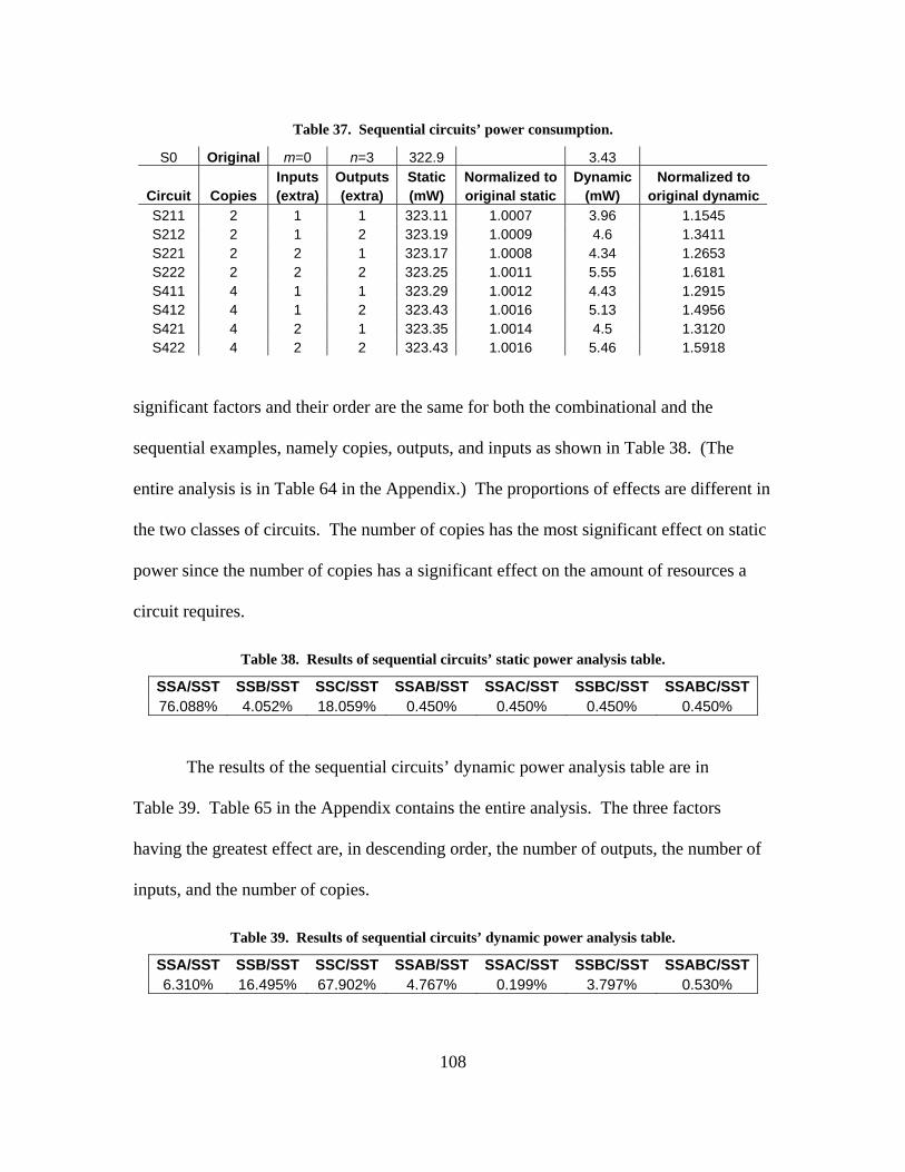
108
Table 37. Sequential circuits’ power consumption.
S0 Original m=0 n=3 322.9 3.43 Inputs Outputs Static Normalized to Dynamic Normalized to
Circuit Copies (extra) (extra) (mW) original static (mW) original dynamic S211 2 1 1 323.11 1.0007 3.96 1.1545 S212 2 1 2 323.19 1.0009 4.6 1.3411 S221 2 2 1 323.17 1.0008 4.34 1.2653 S222 2 2 2 323.25 1.0011 5.55 1.6181 S411 4 1 1 323.29 1.0012 4.43 1.2915 S412 4 1 2 323.43 1.0016 5.13 1.4956 S421 4 2 1 323.35 1.0014 4.5 1.3120 S422 4 2 2 323.43 1.0016 5.46 1.5918
significant factors and their order are the same for both the combinational and the
sequential examples, namely copies, outputs, and inputs as shown in Table 38. (The
entire analysis is in Table 64 in the Appendix.) The proportions of effects are different in
the two classes of circuits. The number of copies has the most significant effect on static
power since the number of copies has a significant effect on the amount of resources a
circuit requires.
Table 38. Results of sequential circuits’ static power analysis table.
SSA/SST SSB/SST SSC/SST SSAB/SST SSAC/SST SSBC/SST SSABC/SST76.088% 4.052% 18.059% 0.450% 0.450% 0.450% 0.450%
The results of the sequential circuits’ dynamic power analysis table are in
Table 39. Table 65 in the Appendix contains the entire analysis. The three factors
having the greatest effect are, in descending order, the number of outputs, the number of
inputs, and the number of copies.
Table 39. Results of sequential circuits’ dynamic power analysis table.
SSA/SST SSB/SST SSC/SST SSAB/SST SSAC/SST SSBC/SST SSABC/SST6.310% 16.495% 67.902% 4.767% 0.199% 3.797% 0.530%

109
5.4.4 VHDL and Partial Scrambling
The existing VHDL and partially scrambled circuits are simulated for 640 ns
each. Table 40 shows the power measurements for the original and modified VHDL
circuits. The power measurements of the original and partially scrambled circuits are in
Table 41. The modified VHDL circuit’s more than 300% increase in dynamic power
over the original circuit’s metric is due to its considerable increase in FPGA resources.
Table 40. VHDL circuits’ power consumption.
VHDL Original m=4 n=2 322.94 1.56 Inputs Outputs Static Normalized to Dynamic Normalized to
Copies (extra) (extra) (mW) original static (mW) original dynamic2 1 2 323.27 1.001 4.88 3.128
Table 41. Partially scrambled circuits’ power consumption.
Partial Original 6 4 323.08 4.27 Inputs Outputs Static Normalized to Dynamic Normalized to
Copies (extra) (extra) (mW) original static (mW) original dynamic2 1 2 323.49 1.001 4.74 1.11 5.4.5 Observations
There is a strong correlation between the number of pins used for a circuit and the
static power consumed by that circuit. Figure 34 illustrates this correlation. This plot
considers all circuits tested and duplicate measurements are deleted. The reason for this
correlation is due to the number of copies. The number of copies impacts the number of
required multiplexer select signals.
Sorting the circuits according to pin count, as was done to produce Figure 34,
results in combinational/sequential pairs of the same copy/extra input/extra output
configuration. These groupings lend credence to the hypothesis that the number of copies

110
R2 = 0.9718
322.5
322.6
322.7
322.8
322.9
323
323.1
323.2
323.3
323.4
323.5
323.6
4 5 6 7 7 10 11 11 12 12 13 13 14 14 14 15 15 15 16 17 18 18 19 19 20
Pins
Stat
ic P
ower
(mW
)
Static PowerLinear (Static Power)
Figure 34. Correlation between pin count and static power.
significantly impacts that number of pins required, which impacts the amount of static
power dissipated.
Sorting the tested circuits in order of dynamic power consumption leads to
groupings of sequential circuits and groupings of combinational circuits. These
groupings seem to indicate that dynamic power dissipation is circuit-dependent.
5.5 Resource Usage
Resource usage metrics are collected from a Quartus II compilation report, the
design’s “.map.rpt” file. The compilations are not optimized for resource usage. For all
circuits, the numbers of LUTs and pins are collected. For sequential circuits, the number
of registers is also collected.

111
5.5.1 Combination Lock
The resource usage of each Combination Lock is listed in Table 42. The number
of pins is solely dependent on the number of inputs. Similarly, the number of registers
depends only the number of states.
Table 42. Combination Locks’ resource usage.
Config States Inputs LUTs Registers PinsCL8-3 8 3 13 9 6 CL8-4 8 4 16 9 7 CL16-3 16 3 25 17 6 CL16-4 16 4 28 17 7
The results of the analysis of the effects of the Combination Locks’ states and
inputs on LUT usage are in Table 43. Table 58 in the Appendix contains the entire
analysis. As expected, the number of states is the greatest contributor to the number of
LUTs required – more states require more logic.
Table 43. Results of Combination Locks’ LUT analysis table.
SSA/SST SSB/SST SSAB/SST94.1176% 5.8824% 0.0000%
5.5.2 Combinational Circuit
The resources used by each test combinational circuit are listed in Table 44. As
expected, circuits with more copies, inputs, and outputs generally require more LUTs and
pins. Also as expected, the required area for a circuit with one extra input and two copies
is less than a 400 percent increase over the original circuit.
For a given number of copies, the increase in LUTs appears to be exponential.
See Figures 35 and 36. Figure 35 shows the increase in LUTs when considering only

112
Table 44. Combinational circuits’ resource usage.
C0 Original m=3 n=2 2 5 Inputs Outputs Normalized to Normalized to
Circuit Copies (extra) (extra) LUTs original LUTs Pins original pins C211 2 1 1 3 1.5 11 2.2 C212 2 1 2 4 2.0 13 2.6 C221 2 2 1 6 3.0 12 2.4 C222 2 2 2 9 4.5 14 2.8 C411 4 1 1 6 3.0 14 2.8 C412 4 1 2 8 4.0 17 3.4 C421 4 2 1 10 5.0 15 3.0 C422 4 2 2 14 7.0 18 3.6
R2 = 0.994
0
1
2
3
4
5
6
7
8
9
10
C211 C212 C221 C222
Circuit
LUTs LUTs
Expon. (LUTs)
Figure 35. Combinational circuits’ LUT increase for circuits 1-4.
circuits C211 through C222. Figure 36 considers circuits C411 through C422. Lines can
also be fit to the same data. However, the resulting R2 values are slightly lower than
those shown in Figures 35 and 36, but still greater than 0.95.

113
R2 = 0.9943
0
2
4
6
8
10
12
14
16
C411 C412 C421 C422
Circuit
LUTs LUTs
Expon. (LUTs)
Figure 36. Combinational circuits’ LUT increase for circuits 5-8.
The metrics for the circuits with two copies appear exponential as they increase
from 3 to 4 to 6 to 9. On the other hand, the data for the circuits with four copies appears
linear, except for the last value, as it increases from 6 to 8 to 10 to 14. More data is
required to conclusively decide whether the increase is exponential or linear.
If the circuits are ordered as in the Subsection 5.4.2, namely C221, C411, C211,
C421, C222, C412, C212, C422, a line fits well to the pin data in Table 44 (cf.,
Figure 37). The order is coherent since adding an input increases the pin count by one,
but adding an output increases the pin count by at least two – one for the output pin and
one for the multiplexer select signal.
The results of the analysis of the combinational circuits’ resource requirements
are in Table 45. Table 62 in the Appendix is the entire analysis. The number of inputs

114
R2 = 0.9644
0
2
4
6
8
10
12
14
16
18
20
C211 C221 C212 C222 C411 C421 C412 C422
Circuit
Pins Pins
Linear (Pins)
Figure 37. Combinational circuits’ pin increase.
Table 45. Results of combinational circuits’ LUT analysis table.
SSA/SST SSB/SST SSC/SST SSAB/SST SSAC/SST SSBC/SST SSABC/SST36.364% 46.023% 14.205% 0.568% 0.568% 2.273% 0.000%
(B) has the greatest impact on LUT usage, followed by the number of copies (A), and the
number of outputs (C). It is expected that the number of inputs has the greatest impact –
adding one extra input to a truth table doubles the size of the table. It is also logical that
number of inputs has a greater effect than the number of copies. Twice as many copies
should double the area. However, as demonstrated in Section 4.5, doubling does not
occur if internal circuit signals are routed appropriately.

115
Table 46 contains the results of the combinational circuits’ pin analysis. The
entire analysis is in Table 63 in the Appendix. The number of copies (A) has the greatest
effect on the number pins used, as stated in Subsection 5.4.5, due to the number of
multiplexer select signals required. The second greatest influence on the number of pins
used is the number of outputs (C), since increasing the number of outputs affects the
number of multiplexer select signals needed.
Table 46. Results of combinational circuits’ pin analysis table.
SSA/SST SSB/SST SSC/SST SSAB/SST SSAC/SST SSBC/SST SSABC/SST62.025% 5.063% 31.646% 0.000% 1.266% 0.000% 0.000%
5.5.3 Sequential Circuit
The resource metrics for the sequential circuits are listed in Table 47. As
expected, the circuits with greater numbers of copies, extra inputs, and extra outputs
generally require more resources. Also as expected, the required area for a circuit with
one extra input and two copies is less than a 400 percent increase over the original circuit.
Table 47. Sequential circuits’ resource usage.
S0 Original m=0 n=3 3 4 Inputs Outputs Normalized to Normalized to
Circuit Copies (extra) (extra) LUTs original LUTs Pins original pins S211 2 1 1 4 1.333 11 2.75 S212 2 1 2 5 1.667 13 3.25 S221 2 2 1 9 3.000 12 3.00 S222 2 2 2 10 3.333 14 3.50 S411 4 1 1 7 2.333 15 3.75 S412 4 1 2 9 3.000 18 4.50 S421 4 2 1 12 4.000 16 4.00 S422 4 2 2 16 5.333 19 4.75
As with the combinational circuits, exponential curves fit better than lines to the
sequential LUT data. The R2 values for the lines are slightly lower than for the

116
exponential curves. More data is required to decide whether the increases in LUTs for
the sequential circuits are linear or exponential. A line fits well to the pin data in
Table 47, with an R2 value greater than that of Figure 37.
In addition to the metrics in Table 47, the number of registers in a circuit is also of
interest. The number of registers in the counter circuits depends only on the total number
of outputs. Hence, a modified circuit with one extra output has four registers and a
modified circuit with two extra outputs has five registers.
Table 48 lists the results of the LUT analysis table for the example sequential
circuits. The entire analysis table is Table 66 in the Appendix. Although in different
proportions than the combinational circuits’ analysis results, the major contributors to
counter LUT usage are, in descending order, the number of inputs (B), the number of
copies (A), and the number of outputs (C). The reasons for these effects are the same as
those stated in the previous subsection.
Table 48. Results of sequential circuits’ LUT analysis table.
SSA/SST SSB/SST SSC/SST SSAB/SST SSAC/SST SSBC/SST SSABC/SST30.769% 58.173% 7.692% 0.481% 1.923% 0.481% 0.481%
The results of the sequential circuits’ pin analysis table are in Table 49. Table 67
in the Appendix is the entire analysis. Similar to the combinational circuits, the two most
significant factors in determining counter pin usage are the number of copies (A) and the
number of outputs (C). The reasons for these effects are the same as those stated in the
previous subsection.

117
Table 49. Results of sequential circuits’ pin analysis table.
SSA/SST SSB/SST SSC/SST SSAB/SST SSAC/SST SSBC/SST SSABC/SST72.973% 3.604% 22.523% 0.000% 0.901% 0.000% 0.000%
5.5.4 VHDL and Partial Scrambling
The resource usage metrics for the original and modified VHDL designs are listed
in Table 50. The increase in LUTs is 400%, which is reasonable for an extra input, two
copies, and two extra outputs. The pin count increases by 233%.
Table 50. VHDL circuits’ resource usage.
VHDL Original m=4 n=2 2 6 Inputs Outputs Normalized to Normalized to
Copies (extra) (extra) LUTs original LUTs Pins original pins 2 1 2 8 4.0 14 2.333
Table 51 lists the resource usage metrics for the original and partially scrambled
circuits. The increase in LUTs is only 200%, even with the combinational multiplexer.
The pin count only doubled.
Table 51. Partially scrambled circuits’ resource usage.
Partial Original 6 4 8 10 Inputs Outputs Normalized to Normalized to
Copies (extra) (extra) LUTs original LUTs Pins original pins 2 1 2 16 2.0 20 2.0
5.6 Combining a Combination Lock with Modified Circuits
To understand the effects of combining a Combination Lock with a modified
circuit, the sixteen-state, four-input Combination Lock (CL16-4) is added to three
different modified circuits. The circuit results in Table 52 are the full adder with two
copies, two extra inputs, and two extra outputs (C222). The counter results with four

118
copies, two extra inputs, and two extra outputs (S422) are shown in Table 53. Table 54 is
for the third circuit with the VHDL design modified to two copies, one extra input, and
two extra outputs.
Table 52. Combination Lock and modified full adder.
Circuit Timing Simulation
time
Static Power (mW)
Dynamic Power (mW) LUTs Registers Pins
Modified full adder (C222) 10.884 ns 320 ns 323.29 6.51 9 0 14 Combination Lock (CL16-4) 271.08 MHz 640 ns 322.98 1.77 28 17 7 Combined 367.24 MHz 960 ns 323.31 4.14 36 17 15
Table 53. Combination Lock and modified counter.
Circuit Timing Simulation
time
Static Power (mW)
Dynamic Power (mW) LUTs Registers Pins
Modified counter (S422) 400 MHz 640 323.43 5.46 16 5 19 Combination Lock (CL16-4) 271.08 MHz 640 322.98 1.77 28 17 7 Combined 326.05 MHz 1280 323.29 3.98 43 22 19
Table 54. Combination Lock and modified VHDL circuit.
Circuit Timing Simulation
time
Static Power (mW)
Dynamic Power (mW) LUTs Registers Pins
Modified VHDL 10.592 ns 640 323.27 4.88 8 0 14 Combination Lock (CL16-4) 271.08 MHz 640 322.98 1.77 28 17 7 Combined 298.33 1280 323.29 3.98 36 17 15
The clock frequency increases for the Combination Lock when combined with the
other circuits due to different routing and resource sharing. The clock frequency

119
decreases for the counter, but this can be remedied by partitioning the two modules and
providing separate clocks to the two modules.
In Tables 52 and 53, the LUT usage is one less than adding the LUT usages of
two components, due to resource sharing. In Table 54, the LUT usage is the sum of the
two LUT usages. The registers counts are also added together. The pin counts are not
summed, since some multiplexer select signals are also inputs to the Combination Lock.
The static power measurements of the components and the combination are within
0.5 mW of each other. The combination of the modules has lower dynamic power
consumption, but that may be due to the simulation file characteristics.
Overall, the combinations of the components meet the expectations for resource
usage and power dissipation. The timing issues can be addressed with partitioning.
5.7 Summary
This chapter gives the results of the tests and explanations of these results.
Significant increases in security can be achieved by applying the proposed circuit design
methodology to digital circuit designs, especially since security increases exponentially
with additional copies, inputs, and outputs. Although the execution times for the
combinational circuits are increasing, the additional level of delay is at most one LUT.
The modified sequential circuits maintain the clock frequency of the original sequential
circuit. More execution time data from larger circuits are needed to better characterize
the effects of the algorithm. Static power consumption appears to be linear with
increases in the size of the modified circuits, and is linearly correlated to design pin
count. Dynamic power dissipation depends on the specific circuit and simulation file.

120
More data are required to determine whether LUT usage increases linearly or
exponentially as circuit sizes increase. Pin count increases linearly and is most affected
by the number of copies.
The examples of this chapter and their test results illustrate the relatively low cost
of operating a design secured by the design modification algorithm. This low cost is a
great value given the substantial increase in security obtained.
The examples also illustrate the flexibility of the design methodology to be
applied in various ways to circuits described in various ways – complete or partial circuit
modification; and by truth or state tables, or already written in VHDL.

121
6. Conclusions and Recommendations
6.1 Chapter Overview
This chapter contains the conclusions of the research and their significance.
Recommendations for future research are also listed. Finally, a summary concludes the
chapter.
6.2 Conclusions of Research
This research found that there is not a standard classification for tampering attacks
and countermeasures. Previous classifications have weaknesses or have been
misinterpreted and misapplied. In addition, there is no clear correlation of
countermeasures to attacks.
Due to this finding, a classification of threats and countermeasures and their
correlation is proposed. The classification addresses some of the weaknesses of previous
classifications. Significant aspects of the classification are the categorization of attacks,
rather than attackers, and the use of both cost and time for the taxonomy. With the
proposed classification, attacks and countermeasures are correlated. However, there are
still no quantified costs and times for attacks nor similar measures for countermeasures.
This research developed a circuit design modification methodology that provides
significant security gains over an original circuit without considerable performance costs.
Thus, the reverse engineering vulnerability of an FPGA design can be significantly
reduced without corresponding penalties to its operation. This research also provides a
proof of concept for the algorithm by modifying and testing several circuits, to include
the modification of only a portion of a circuit. The modified sequential circuits maintain

122
the original circuit’s clock frequency. The execution time of the modified combinational
circuits increases by the delay of one level of LUTs at most over the original execution
time. Static power consumption, the main component of power consumption in the tests
conducted, increases linearly with the number of circuit copies or pins. Pin count
increases linearly with increases in modified circuit size. LUT usage may increase
linearly or exponentially – more data are required to determine the growth rate. The tests
show that the increase in the number of LUTs is at or below what might be expected for
added copies, inputs, and outputs.
6.3 Significance of Research
The proposed classification provides a method to apply appropriate
countermeasures to perceived threats. With properly classified threats, suitable measures
can be applied to counter those threats.
The circuit design modification methodology protects critical technologies and
information. This in turn maintains the nation’s technological advantage and provides
many years of weapons systems use.
6.4 Recommendations for Action
It is recommended that the Air Force Research Laboratory’s (AFRL) Anti-
Tamper – Software Protection Initiative (AT-SPI) Technology Office evaluate the merit
of the proposed methodology. The portions of the methodology found to have merit
should be implemented by the Department of Defense.
123
6.5 Recommendations for Future Research
Based on the knowledge and experience gained from this study, there are several
areas that can be explored further.
The lack of quantified costs and durations of attacks and countermeasures
indicates a need to collect such metrics. These metrics can refine the proposed
classification and the application of appropriate countermeasures to threats.
Scripts or a program could be written to automate the processing of circuits
according to the proposed design modification algorithm.
The use of bidirectional pins is not addressed in this study. Incorporating
bidirectional pins into the algorithm would be useful.
The application of the methodology to ASICs would uncover any ASIC-specific
implementation problems.
Applying the algorithm to larger circuits and testing their security by attacking the
modified circuits are additional avenues to pursue. A specific large-circuit issue is the
scrambling of multiple modules of VHDL. Each module could be scrambled and
interfaced with other individually scrambled modules. An alternative is to treat the
collection of modules as a single black box.
The explicit intertwining of valid circuits with decoy circuits was not specifically
addressed in this study. Studying this technique further could aid in other aspects of anti-
reverse engineering.
Finally, additional research could extend the design algorithm to pipelined
circuits. Specifically, scrambling and interfacing each stage or deciding what portions of

124
the circuit must be modified are of interest. The application of the procedure to larger
circuits and explicit intertwining may be useful in pipelined designs.
6.6 Summary
This chapter presents the conclusions of this research and its significance,
focusing on the classification of threats and countermeasures and the design modification
algorithm. It is recommended that AFRL’s AT-SPI Technology Office evaluate the
algorithm. Further study, including the refinement of cost and time values of attacks and
countermeasures and the application of the design methodology to ASICs and multicycle
designs, is also proposed.
The proposed design modification method is found to be economical in terms of
the security gained and performance costs incurred.

125
Appendix: Data Analysis Tables
Table 55. Analysis of Combination Locks’ maximum frequencies.
Effect i I A (states) B (inputs) AB yi
(config) (mean) 8=-1, 16=1 3=-1, 4=1 (interaction) (fmax) (yi-ybar)^2CL8-3 1 -1 -1 1 379.36 1005.5241 CL8-4 1 -1 1 -1 354.36 45.0241 CL16-3 1 1 -1 -1 385.8 1455.4225 CL16-4 1 1 1 1 271.08 5862.9649 Total 1390.60 -76.84 -139.72 -89.72 1390.60 =sum
Total/4 347.65 -19.21 -34.93 -22.43 347.65 =ybar SST= SSA= SSB= SSAB= 8368.936 1476.096 4880.420 2012.420 SSA/SST= SSB/SST= SSAB/SST= 17.6378% 58.3159% 24.0463%
Table 56. Analysis of Combination Locks’ static power consumptions.
Effect i I A (states) B (inputs) AB yi
(config) (mean) 8=-1, 16=1 3=-1, 4=1 (interaction) (mW) (yi-ybar)^2CL8-3 1 -1 -1 1 322.94 0.0003063 CL8-4 1 -1 1 -1 322.97 0.0001562 CL16-3 1 1 -1 -1 322.94 0.0003063 CL16-4 1 1 1 1 322.98 0.0005062 Total 1291.83 0.01 0.07 0.01 1291.83 =sum
Total/4 322.9575 0.0025 0.0175 0.0025 322.9575 =ybar SST= SSA= SSB= SSAB= 0.001275 0.000025 0.001225 0.000025 SSA/SST= SSB/SST= SSAB/SST= 1.9608% 96.0784% 1.9608%

126
Table 57. Analysis of Combination Locks’ dynamic power consumptions.
Effect i I A (states) B (inputs) AB yi
(config) (mean) 8=-1, 16=1 3=-1, 4=1 (interaction) (mW) (yi-ybar)^2 CL8-3 1 -1 -1 1 1.97 0.005625 CL8-4 1 -1 1 -1 2.1 0.042025 CL16-3 1 1 -1 -1 1.74 0.024025 CL16-4 1 1 1 1 1.77 0.015625 Total 7.58 -0.56 0.16 -0.10 7.58 =sum
Total/4 1.895 -0.140 0.040 -0.025 1.895 =ybar SST= SSA= SSB= SSAB= 0.0873 0.0784 0.0064 0.0025 SSA/SST= SSB/SST= SSAB/SST= 89.8053% 7.3310% 2.8637%
Table 58. Analysis of Combination Locks’ LUT usages.
Effect i I A (states) B (inputs) AB yi
(config) (mean) 8=-1, 16=1 3=-1, 4=1 (interaction) (LUTs) (yi-ybar)^2CL8-3 1 -1 -1 1 13 56.25 CL8-4 1 -1 1 -1 16 20.25 CL16-3 1 1 -1 -1 25 20.25 CL16-4 1 1 1 1 28 56.25 Total 82.0 24.0 6.0 0.0 82.0 =sum
Total/4 20.5 6.0 1.5 0.0 20.5 =ybar SST= SSA= SSB= SSAB= 153.0 144.0 9.0 0.0 SSA/SST= SSB/SST= SSAB/SST= 94.1176% 5.8824% 0.0000%

127
Table 59. Analysis of combinational circuits’ execution times.

128
Table 60. Analysis of combinational circuits’ static power consumptions.

129
Table 61. Analysis of combinational circuits’ dynamic power consumptions.

130
Table 62. Analysis of combinational circuits’ LUT usages.

131
Table 63. Analysis of combinational circuits’ pin usages.

132
Table 64. Analysis of sequential circuits’ static power consumptions.

133
Table 65. Analysis of sequential circuits’ dynamic power consumptions.

134
Table 66. Analysis of sequential circuits’ LUT usages.

135
Table 67. Analysis of sequential circuits’ pin usages.

136
Bibliography
[ACA02] Avery, L., J. Crabbe, S. Al Sofi, H. Ahmed, J. Cleaver, and D. Weaver. “Reverse Engineering Complex Application-Specific Integrated Circuits (ASICs),” Proceedings of the DMSMS 2002 Conference. 25-28 March 2002. http://smaplab.ri.uah.edu/dmsms02/proceed.htm, 18 January 2006.
[Act02] Actel Corporation. “Design Security with Actel FPGAs.” August 2002. http://www.actel.com/documents/DesignSecurityPPT.pdf, 20 January 2006.
[Act06] Actel Corporation. “FuseLock: Security in Actel Antifuse FPGAs.” Copyright 2006. http://www.actel.com/products/rescenter/security/solutions/antifuse.aspx, 16 January 2006.
[ADD91] Abraham, D., G. Dolan, P. Double, and J. Stevens. “Transaction Security System,” IBM Systems Journal, 30(2):206-209 (1991). http://www.research.ibm.com/journal/sj/302/ibmsj3002G.pdf, 20 January 2006.
[AFR05] Air Force Research Laboratory. Research Proposal, AF 05.1 Topic Descriptions, “Active Decoy Circuits.” Wright-Patterson AFB OH, January 2005.
[Alt05] Altera Corporation. Stratix Device Handbook, Volume 1, version 3.3. July 2005. http://www.altera.com/literature/lit-stx.jsp, 16 January 2006.
[Ang06] “Akuma Presents…Programming Jargon….” http://www.angelfire.com/anime3/internet/programming.htm, 17 January 2006.
[AnK96] Anderson, R. and M. Kuhn. “Tamper Resistance – a Cautionary Note,” The Second USENIX Workshop on Electronic Commerce Proceedings, 1-11. Oakland CA, 18-21 November 1996.
[AnK97] Anderson, R. and M. Kuhn. “Low Cost Attacks on Tamper Resistant Devices,” Security Protocols, 5th International Workshop, Proceedings, Springer LNCS 1361, 125-136. Paris France, 7-9 April 1997.
[BrR96] Brown, S. and J. Rose. “FPGA and CPLD Architectures: A Tutorial,” IEEE Design and Test of Computers, 42-57 (Summer 1996).

137
[CEL99] Chisholm, G., S. Eckmann, C. Lain, and R. Veroff. “Understanding Integrated Circuits,” IEEE Design and Test of Computers, 26-37 (April-June 1999).
[DoD01] United States Department of Defense. DoD News Briefing, Rear Admiral Craig R. Quigley DASD PA. 3 April 2001. http://www.defenselink.mil/transcripts/2001/t04032001_t403dasd.html, 17 February 2006.
[EFF98] Electronic Frontier Foundation, “‘EFF DES Cracker’ Machine Brings Honesty to Crypto Device: Electronic Frontier Foundation Proves That DES Is Not Secure.” 17 July 1998. http://www.eff.org/Privacy/Crypto/Crypto_misc/DESCracker/HTML/19980716_eff_descracker_pressrel.html, 20 January 2006.
[ETS05] Elbaz, R., L. Torres, G. Sassatelli, P. Guillemin, C. Anguille, C. Buatois, and J.B. Rigaud. “Hardware Engines for Bus Encryption: a Survey of Existing Techniques,” Proceedings of the Design, Automation and Test in Europe Conference and Exhibition (DATE’05). 3: 40- 45. 7-11 March 2005.
[FAS00] Federation of American Scientists. Military Analysis Network, F-117A Nighthawk. 23 April 2000. http://www.fas.org/man/dod-101/sys/ac/f-117.htm, 10 January 2006.
[FBI06] Federal Bureau of Investigation. “The Atom Spy Case.” http://www.fbi.gov/libref/historic/famcases/atom/atom.htm, 20 January 2006.
[Geo05] GeoConnections Secretariat. Geomatics Canada Intellectual Property, Glossary of Selected Terms, 16 June 2005. http://www.geoconnections.org/CGDI.cfm/fuseaction/policySupporting.seeFile/id/95/print/Y/gcs.cfm, 17 January 2006.
[GLL05] Gordon, L., M. Loeb, W. Lucyshyn, and R. Richardson. 2005 CSI/FBI Computer Crime and Security Survey, 2005.
[Gut01] Gutmann, P. “Data Remanence in Semiconductor Devices,” Proceedings of the 10th USENIX Security Symposium. Washington DC, 13-17 August 2001.

138
[Hod05] Hodson, D. Class files, CSCE 687, Advanced Microprocessor Design Laboratory. Graduate School of Engineering and Management, Air Force Institute of Technology, Wright-Patterson AFB OH, Summer Quarter 2005.
[HuS99] Huber, A. and J. Scott. “The Role and Nature of Anti-Tamper Techniques in U.S. Defense Acquisition,” Acquisition Review Quarterly, 355-367 (Fall 1999).
[IBM06] IBM. “IBM PCI Cryptographic Coprocessor.” http://www-03.ibm.com/security/cryptocards/pcicc/overhardware.shtml, 20 January 2006.
[IEEE93] The Institute of Electrical and Electronics Engineers, Inc. IEEE Recommended Practice for Futurebus+. IEEE Std 896.3-1993. 13 October 1993.
[J-STD95] The Institute of Electrical and Electronics Engineers, Inc. and Electronic Industries Association. Trial-Use Standard: Standard for Information Technology Software Life Cycle Processes: Software Development Acquirer-Supplier Agreement. J-STD-016-1995. 30 September 1995.
[JYP03] Jain, A., L. Yuan, P. Pari, and G. Qu. “Zero Overhead Watermarking Technique for FPGA Designs,” Proceedings of the 13th ACM Great Lakes Symposium on VLSI, 147-152. Washington DC, 28-29 April 2003.
[Kea01] Kean, T. “Secure Configuration of a Field Programmable Gate Array,” Proceedings of the 9th Annual IEEE Symposium on Field-Programmable Custom Computing Machines (FCCM’01), 259-260. 2001.
[Kim05] Kim, Y. “EENG 695 VHDL.” CD-ROM. 2005.
[Lam02] Lambeth, B. “Kosovo and the Continuing SEAD Challenge,” Aerospace Power Journal, 8-21 (Summer 2002). http://www.airpower.maxwell.af.mil/airchronicles/apj/apj02/sum02/sum02.html, 10 January 2006.
[Mis01] Mishchenko, A. “Two Level Sum-of-Product Minimization.” http://www.ee.pdx.edu/~alanmi/research/min/minSop.htm, 17 February 2006.
[MIT01] 6.004 Computation Structures. Lecture notes, Fall 2001. http://6004.csail.mit.edu/Fall01/handouts/L07-4up.pdf, 17 February 2006.

139
[NPS03] Neve, M.; E. Peeters; D. Samyde; and J.-J. Quisquater. “Memories: a Survey of their Secure Uses in Smart Cards,” Proceedings of the Second IEEE International Security in Storage Workshop (SISW’03). 31 October 2003.
[New01] NewsMax.com. “Admiral Worried That China Is Holding U.S. Servicemen.” 2 April 2001. http://www.newsmax.com/archives/articles/2001/4/1/223300.shtml, 17 February 2006.
[NIS02] National Institute of Standards and Technology. Security Requirements for Cryptographic Modules. FIPS PUB 140-2. 25 May 2001. http://csrc.nist.gov/publications/fips/fips140-2/fips1402.pdf, 20 January 2006.
[PaS05] Park, T. and K. Shin. “Soft Tamper-Proofing via Program Integrity Verification in Wireless Sensor Networks,” IEEE Transactions on Mobile Computing, 4(3):297- 309 (May/June 2005).
[Pri05] Princeton University, WordNet® 2.1 Copyright 2005 by Princeton University. http://wordnet.princeton.edu/perl/webwn, 17 January 2006.
[RRC04] Ravi, S., A. Raghunathan, and S. Chakradhar. “Tamper Resistance Mechanisms for Secure Embedded Systems,” Proceedings of the 17th International Conference on VLSI Design (VLSID’04), 605-611. 2004.
[Smi01] Smith, C. “China Broke U.S. Military Codes After Taking Plane.” 8 June 2001. http://www.newsmax.com/archives/articles/2001/6/7/193114.shtml, 17 February 2006.
[SoA93] Soden, J. and R. Anderson. “IC Failure Analysis: Techniques and Tools for Quality and Reliability Improvement,” Proceedings of the IEEE, 81(5):703-715 (May 1993).
[Tri01] EP-3E image. http://members.tripod.com/mwaviation/images/EP-3E%20damaged%20&%20captured%20in%20China.jpg, 17 February 2006.
[Xil05] Xilinx, Inc. Virtex-II Pro and Virtex-II Pro X Platform FPGAs: Complete Data Sheet, version 4.5. 10 October 2005. http://www.xilinx.com/bvdocs/publications/ds083.pdf, 17 February 2006.

140
[Ver01] Verton, D. “FBI spy case highlights insider threat to corporate data,” Computerworld. 21 February 2001. http://www.computerworld.com/securitytopics/security/story/0,10801,57889,00.html, 20 January 2006.
[WGP04] Wollinger, T., J. Guarjardo, and C. Paar. “Security on FPGAs: State-of-the-Art Implementations and Attacks,” ACM Transactions on Embedded Computing Systems, 3(3):534-574 (August 2004).

141
Vita
Bradley D. Christiansen was born in Provo, Utah, in May 1971. His parents
relocated soon thereafter to Payson, Utah, where they reared Brad. He graduated from
Payson High School in May 1989. In the Fall of that same year, Brad began his pursuit
toward a bachelor’s degree in electrical engineering at Brigham Young University (BYU)
in Provo, Utah. After his freshman year, Brad served a two-year Church mission to
Massachusetts among Portuguese-speaking people. Following his mission, he continued
his studies at BYU and participated in the Air Force Reserve Officer Training Corps. He
graduated and was commissioned a second lieutenant in the United States Air Force in
December 1995. Brad entered active duty in February 1996 and had several assignments
prior to being assigned to the Air Force Institute of Technology as a master’s degree
student in August 2004.

REPORT DOCUMENTATION PAGE Form Approved OMB No. 074-0188
The public reporting burden for this collection of information is estimated to average 1 hour per response, including the time for reviewing instructions, searching existing data sources, gathering and maintaining the data needed, and completing and reviewing the collection of information. Send comments regarding this burden estimate or any other aspect of the collection of information, including suggestions for reducing this burden to Department of Defense, Washington Headquarters Services, Directorate for Information Operations and Reports (0704-0188), 1215 Jefferson Davis Highway, Suite 1204, Arlington, VA 22202-4302. Respondents should be aware that notwithstanding any other provision of law, no person shall be subject to an penalty for failing to comply with a collection of information if it does not display a currently valid OMB control number. PLEASE DO NOT RETURN YOUR FORM TO THE ABOVE ADDRESS. 1. REPORT DATE (DD-MM-YYYY) 23-03- 2006
2. REPORT TYPE Master’s Thesis
3. DATES COVERED (From – To) March 2005 - March 2006
5a. CONTRACT NUMBER 5b. GRANT NUMBER 2005-088
4. TITLE AND SUBTITLE Active FPGA Security Through Decoy Circuits 5c. PROGRAM ELEMENT NUMBER
5d. PROJECT NUMBER 5e. TASK NUMBER
6. AUTHOR(S) Christiansen, Bradley D., Major, USAF
5f. WORK UNIT NUMBER
7. PERFORMING ORGANIZATION NAMES(S) AND ADDRESS(S) Air Force Institute of Technology Graduate School of Engineering and Management (AFIT/EN) 2950 Hobson Way WPAFB OH 45433-7765
8. PERFORMING ORGANIZATION REPORT NUMBER AFIT/GE/ENG/06-15
10. SPONSOR/MONITOR’S ACRONYM(S)
9. SPONSORING/MONITORING AGENCY NAME(S) AND ADDRESS(ES) AFRL/SNTA (AFMC), ATTN: Dr. Robert W. Bennington AT-SPI Technology Office, 2241 Avionics Circle WPAFB OH 43433 Phone: 937-320-9068 Email: [email protected]
11. SPONSOR/MONITOR’S REPORT NUMBER(S)
12. DISTRIBUTION/AVAILABILITY STATEMENT APPROVED FOR PUBLIC RELEASE; DISTRIBUTION IS UNLIMITED
13. SUPPLEMENTARY NOTES 14. ABSTRACT Field Programmable Gate Arrays (FPGAs) based on Static Random Access Memory (SRAM) are vulnerable to tampering attacks such as readback and cloning attacks. Such attacks enable the reverse engineering of the design programmed into an FPGA. To counter such attacks, measures that protect the design with low performance penalties should be employed.
This research proposes a method which employs the addition of active decoy circuits to protect SRAM FPGAs from reverse engineering. The effects of the protection method on security, execution time, power consumption, and FPGA resource usage are quantified. The method significantly increases the security of the design with only minor increases in execution time, power consumption, and resource usage. For the circuits used to characterize the method, security increased to more than one million times the original values, while execution time increased to at most 1.2 times, dynamic power consumption increased to at most two times, and look-up table usage increased to at most seven times the original values. These are reasonable penalties given the size and security of the modified circuits. The proposed design protection method also extends to FPGAs based on other technologies and to Application-Specific Integrated Circuits (ASICs).
In addition to the design methodology proposed, a new classification of tampering attacks and countermeasures is presented.
15. SUBJECT TERMS Computer Security, Integrated Circuits, Digital Systems, Reverse Engineering, FPGA, Decoy Circuits
16. SECURITY CLASSIFICATION OF:
19a. NAME OF RESPONSIBLE PERSON Yong C. Kim, PhD (ENG)
REPORT U
ABSTRACT U
c. THIS PAGE U
17. LIMITATION OF ABSTRACT UU
18. NUMBER OF PAGES 158 19b. TELEPHONE NUMBER (Include area code)
(937) 255-3636 ext 4620; email: [email protected]
Standard Form 298 (Rev: 8-98) Prescribed by ANSI Std. Z39-18