Embed Size (px)
Citation preview
[AK4588]
MS0287-E-03 2009/05 - 1 -
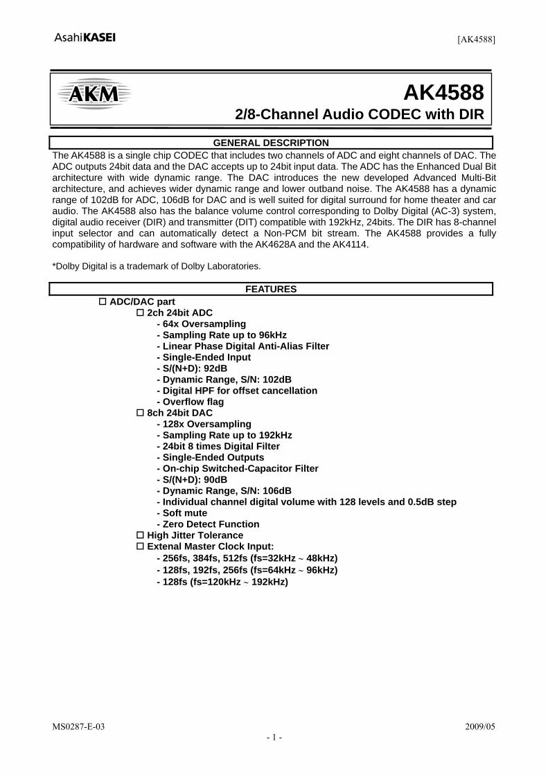
GENERAL DESCRIPTION The AK4588 is a single chip CODEC that includes two channels of ADC and eight channels of DAC. The ADC outputs 24bit data and the DAC accepts up to 24bit input data. The ADC has the Enhanced Dual Bit architecture with wide dynamic range. The DAC introduces the new developed Advanced Multi-Bit architecture, and achieves wider dynamic range and lower outband noise. The AK4588 has a dynamic range of 102dB for ADC, 106dB for DAC and is well suited for digital surround for home theater and car audio. The AK4588 also has the balance volume control corresponding to Dolby Digital (AC-3) system, digital audio receiver (DIR) and transmitter (DIT) compatible with 192kHz, 24bits. The DIR has 8-channel input selector and can automatically detect a Non-PCM bit stream. The AK4588 provides a fully compatibility of hardware and software with the AK4628A and the AK4114. *Dolby Digital is a trademark of Dolby Laboratories.
FEATURES ADC/DAC part
2ch 24bit ADC - 64x Oversampling - Sampling Rate up to 96kHz - Linear Phase Digital Anti-Alias Filter - Single-Ended Input - S/(N+D): 92dB - Dynamic Range, S/N: 102dB - Digital HPF for offset cancellation - Overflow flag
8ch 24bit DAC - 128x Oversampling - Sampling Rate up to 192kHz - 24bit 8 times Digital Filter - Single-Ended Outputs - On-chip Switched-Capacitor Filter - S/(N+D): 90dB - Dynamic Range, S/N: 106dB - Individual channel digital volume with 128 levels and 0.5dB step - Soft mute - Zero Detect Function
High Jitter Tolerance Extenal Master Clock Input:
- 256fs, 384fs, 512fs (fs=32kHz ∼ 48kHz) - 128fs, 192fs, 256fs (fs=64kHz ∼ 96kHz) - 128fs (fs=120kHz ∼ 192kHz)
2/8-Channel Audio CODEC with DIRAK4588

[AK4588]
MS0287-E-03 2009/05 - 2 -
DIR/DIT Part AES3, IEC60958, S/PDIF, EIAJ CP1201 Compatible Low jitter Analog PLL PLL Lock Range : 32kHz to 192kHz Clock Source: PLL or X'tal 8-channel Receiver input 2-channel Transmission output (Through output or DIT) Auxiliary digital input De-emphasis for 32kHz, 44.1kHz, 48kHz and 96kHz Detection Functions
- Non-PCM Bit Stream Detection - DTS-CD Bit Stream Detection - Sampling Frequency Detection
(32kHz, 44.1kHz, 48kHz, 88.2kHz, 96kHz, 176.4kHz, 192kHz) - Unlock & Parity Error Detection - Validity Flag Detection
Up to 24bit Audio Data Format Audio I/F: Master or Slave Mode 40-bit Channel Status Buffer Burst Preamble bit Pc and Pd Buffer for Non-PCM bit stream Q-subcode Buffer for CD bit stream Serial μP I/F Two Master Clock Outputs: 64fs/128fs/256fs/512fs
TTL Level Digital I/F 4-wire Serial and I2C Bus μP I/F for mode setting Operating Voltage: 4.5 to 5.5V with 5V tolerance Power Supply for output buffer: 2.7 to 5.5V 80pin LQFP Package (0.5mm pitch)
[AK4588]
MS0287-E-03 2009/05 - 3 -
■ Block Diagram
Input
Selector
ClockRecovery Clock
Generator
DAIF
Decoder
AC-3/MPEG
Detect
DEM
μP I/F
Audio I/F
X'talOscillator
PDN
INT0
LRCK2BICK2SDTO2
DAUX2
MCKO2
XTOXTIRPVDDPVSS
CDTICDTOCCLKCSNDVDD
DVSS TVDD
MCKO1
I2C
RX0 RX1 RX2 RX3 RX4 RX5 RX6 RX7
DIT
TX0
Error &
DetectSTATUS
INT1
Q-subcode buffer
TX1
B,C,U, VOUT
8 to 3
VIN
AudioI/F
LPF
LPF
LPF
LPF
LPF
LPF
LOUT1
ROUT1
LOUT2
ROUT2
LOUT3
ROUT3
DAC DATTDEM
ADC HPF
ADC HPFRIN
LIN
LRCK1BICK1
SDTI1 SDTI2 SDTI3
DAUX1
MCLK
LRCKBICK
SDOUT
SDIN1SDIN2SDIN3
MCLK
SDTO1
Format Converter
SDTI4 SDIN4LPF
LPF
LOUT4
ROUT4
DAC DATTDEM
DAC DATTDEM
DAC DATTDEM
DAC DATTDEM
DAC DATTDEM
DAC DATTDEM
DAC DATTDEM
AVDD AVSS

[AK4588]
MS0287-E-03 2009/05 - 4 -
■ Ordering Guide
AK4588VQ -40 ∼ +85°C 80pin LQFP(0.5mm pitch) AKD4588 Evaluation Board for AK4588
■ Pin Layout
(Top View)
INT1
B
OU
T TV
DD
D
VDD
D
VSS
X
TO
XTI
TE
ST3
M
CK
O2
MC
KO
1 C
OU
T U
OU
T V
OU
T S
DTO
2 B
ICK
2 LR
CK
2 S
DTO
1 B
ICK
1 LR
CK
1 C
DTO
1 2 3 4 5 6 7 8 9 10
11
12
13
14
15
16
17
18
19
20
40 39 38 37 36 35 34 33 32 31 30 29 28 27 26 25 24 23 22 21
60
59
58
57
56
55
54
53
52
51
50
49
48
47
46
45
44
43
42
41
61 62 63 64 65 66 67 68 69 70 71 72 73 74 75 76 77 78 79 80
RX2 NC
RX3 PVSS
R PVDD
RX4 TEST2
RX5 CAD0
RX6 CAD1
RX7 I2C
DAUX2 VIN
MCLK TX0 TX1
INT0
NC LOUT3 NC ROUT4 NC LOUT4 DZF1 DZF2 MASTER PDN XTL0 XTL1 SDTI1 SDTI2 SDTI3 SDTI4 DAUX1 CSN CDTI/SDA CCLK/SCL
TES
T1
RX1
N
C
RX0
AV
SS
AVD
D
VR
EFH
V
CO
M
RIN
LI
N
NC
R
OU
T1
NC
LO
UT1
N
C
RO
UT2
N
C
LOU
T2
NC
R
OU
T3

[AK4588]
MS0287-E-03 2009/05 - 5 -
■ Compatibility with AK4628 + AK4114
Functions AK4628+ AK4114 AK4588 Parallel control mode Yes No TDM0, DFS0, DZFE, SDOS, SMUTE pins
Available Not available
AK4628: Set by CAD1/0 pins ADC/DAC part: Set by CAD1/0 pins4 wire serial (I2C pin= “L”) AK4114: Fixed to “00” DIR/DIT part: Fixed to “00”
AK4628: Set by CAD1/0 pins ADC/DAC part: Set by CAD1/0 pins
Chip address(*)
I2C Bus (I2C pin = “H”) AK4114: Set by CAD1/0 pins DIR/DIT part: Fixed to “00”
(*) The AK4588 has two register maps including ADC/DAC part (compatible with the AK4628) and DIR/DIT part (compatible with the AK4114). Each register is selected by Chip Address.
[AK4588]
MS0287-E-03 2009/05 - 6 -
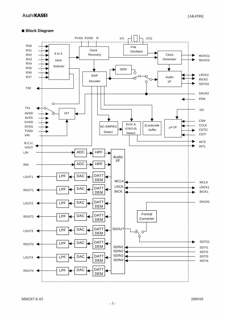
PIN/FUNCTION No. Pin Name I/O Function 1 INT1 O Interrupt 1 Pin
2 BOUT O Block-Start Output Pin for Receiver Input “H” during first 40 flames.
3 TVDD - Output Buffer Power Supply Pin, 2.7V∼5.5V 4 DVDD - Digital Power Supply Pin, 4.5V∼5.5V 5 DVSS - Digital Ground Pin 6 XTO O X'tal clock Output Pin 7 XTI I X'tal / External clock Input Pin
8 TEST3 I Test 3 Pin This pin should be connected to DVSS.
9 MCKO2 O Master Clock Output 2 Pin 10 MCKO1 O Master Clock Output 1 Pin 11 COUT O C-bit Output Pin for Receiver Input 12 UOUT O U-bit Output Pin for Receiver Input 13 VOUT O V-bit Output Pin for Receiver Input 14 SDTO2 O Audio Serial Data Output Pin (DIR/DIT part) 15 BICK2 I/O Audio Serial Data Clock Pin (DIR/DIT part) 16 LRCK2 I/O Channel Clock Pin (DIR/DIT part) 17 SDTO1 O Audio Serial Data Output Pin (ADC/DAC part) 18 BICK1 I/O Audio Serial Data Clock Pin (ADC/DAC part) 19 LRCK1 I/O Input Channel Clock Pin 20 CDTO O Control Data Output Pin in Serial Mode, I2C pin= “L”.
CCLK I Control Data Clock Pin in Serial Mode, I2C pin= “L” 21 SCL I Control Data Clock Pin in Serial Mode, I2C pin= “H” CDTI I Control Data Input Pin in Serial Mode, I2C pin= “L”. 22 SDA I/O Control Data Pin in Serial Mode, I2C pin= “H”.
I Chip Select Pin in Serial Mode, I2C pin= “L”. 23 CSN I This pin should be connected to DVSS, I2C pin= “H”. 24 DAUX1 I AUX Audio Serial Data Input Pin (ADC/DAC part) 25 SDTI4 I DAC4 Audio Serial Data Input Pin 26 SDTI3 I DAC3 Audio Serial Data Input Pin 27 SDTI2 I DAC2 Audio Serial Data Input Pin 28 SDTI1 I DAC1 Audio Serial Data Input Pin 29 XTL1 I X’tal Frequency Select 0 Pin 30 XTL0 I X’tal Frequency Select 1 Pin

[AK4588]
MS0287-E-03 2009/05 - 7 -
No. Pin Name I/O Function
31 PDN I Power-Down Mode Pin
When “L”, the AK4588 is powered-down, all output pin goes “L”, all registers are reset. When CAD1-0 pins are changed, the AK4588 should be reset by the PDN pin.
32 MASTER I Master Mode Select Pin “H”: Master mode, “L”: Slave mode
DZF2 O
Zero Input Detect 2 Pin (Table 13) When the input data of the group 1 follow total 8192 LRCK cycles with “0” input data, this pin goes to “H”. When RSTN1 bit is “0” or PWDAN bit is “0”, this pin goes to “H”. 33
OVF O Analog Input Overflow Detect Pin
This pin goes to “H” if the analog input of Lch or Rch overflows. This pin becomes OVF pin if OVFE bit is set to 1.
34 DZF1 O
Zero Input Detect 1 Pin (Table 13) When the input data of the group 1 follow total 8192 LRCK cycles with “0” input data, this pin goes to “H”. When RSTN1 bit is “0” or PWDAN bit is “0”, this pin goes to “H”.
35 LOUT4 O DAC4 Lch Analog Output Pin
36 NC - No Connect pin No internal bonding. This pin should be opened.
37 ROUT4 O DAC4 Rch Analog Output Pin
38 NC - No Connect pin No internal bonding. This pin should be opened.
39 LOUT3 O DAC3 Lch Analog Output Pin
40 NC - No Connect pin No internal bonding. This pin should be opened.
41 ROUT3 O DAC3 Rch Analog Output Pin
42 NC - No Connect pin No internal bonding. This pin should be opened.
43 LOUT2 O DAC2 Lch Analog Output Pin
44 NC - No Connect pin No internal bonding. This pin should be opened.
45 ROUT2 O DAC2 Rch Analog Output Pin
46 NC - No Connect pin No internal bonding. This pin should be opened.
47 LOUT1 O DAC1 Lch Analog Output Pin
48 NC - No Connect pin No internal bonding. This pin should be opened.
49 ROUT1 O DAC1 Rch Analog Output Pin
50 NC - No Connect pin No internal bonding. This pin should be opened.
51 LIN I Lch Analog Input Pin 52 RIN I Rch Analog Input Pin
53 VCOM - Common Voltage Output Pin 2.2μF capacitor should be connected to AVSS externally.
54 VREFH - Positive Voltage Reference Input Pin, AVDD

[AK4588]
MS0287-E-03 2009/05 - 8 -
No. Pin Name I/O Function 55 AVDD - Analog Power Supply Pin, 4.5V∼5.5V 56 AVSS - Analog Ground Pin, 0V 57 RX0 I Receiver Channel 0 Pin (Internal biased pin. Internally biased at PVDD/2)
58 NC - No Connect pin No internal bonding. This pin should be connected to PVSS.
59 RX1 I Receiver Channel 1 Pin (Internal biased pin. Internally biased at PVDD/2)
60 TEST1 I Test 1 Pin This pin should be connected to PVSS.
61 RX2 I Receiver Channel 2 Pin (Internal biased pin. Internally biased at PVDD/2)
62 NC - No Connect pin No internal bonding. This pin should be connected to PVSS.
63 RX3 I Receiver Channel 3 Pin (Internal biased pin. Internally biased at PVDD/2) 64 PVSS - PLL Ground pin
65 R - External Resistor Pin 12kΩ +/-1% resistor should be connected to PVSS externally.
66 PVDD - PLL Power supply Pin, 4.5V∼5.5V 67 RX4 I Receiver Channel 4 Pin (Internal biased pin. Internally biased at PVDD/2)
68 TEST2 I Test 2 Pin This pin should be connected to PVSS.
69 RX5 I Receiver Channel 5 Pin (Internal biased pin. Internally biased at PVDD/2) 70 CAD0 I Chip Address 0 Pin (ADC/DAC part) 71 RX6 I Receiver Channel 6 Pin (Internal biased pin. Internally biased at PVDD/2) 72 CAD1 I Chip Address 1 Pin (ADC/DAC part) 73 RX7 I Receiver Channel 7 Pin (Internal biased pin. Internally biased at PVDD/2)
74 I2C I Control Mode Select Pin. “L”: 4-wire Serial, “H”: I2C Bus
75 DAUX2 I Auxiliary Audio Data Input Pin (DIR/DIT part) 76 VIN I V-bit Input Pin for Transmitter Output 77 MCLK I Master Clock Input Pin 78 TX0 O Transmit Channel (Through Data) Output 0 Pin
79 TX1 O Transmit Channel Output1 pin
When TX bit = “0”, Transmit Channel (Through Data) Output 1 Pin. When TX bit = “1”, Transmit Channel (DAUX2 Data) Output Pin (default).
80 INT0 O Interrupt 0 Pin Note: All input pins except internal biased pins and internal pull-down pin should not be left floating.
VCOM
PVDD
PVSS
RX pin 20k(typ)
20k(typ)
Internal biased pin Circuit

[AK4588]
MS0287-E-03 2009/05 - 9 -
■ Handling of Unused Pin The unused I/O pins should be processed appropriately as below. Classification Pin Name Setting Analog RX7-0, LOUT4-1, ROUT4-1, LIN, RIN These pins should be open.
INT1-0, BOUT, XTO, MCKO2-1, COUT, UOUT, VOUT, SDTO2-1, CDTO, DZF2-1, TX1-0
These pins should be open.
CSN, DAUX2-1, SDTI4-1, XTL1-0, TEST3 These pins should be connected to DVSS. Digital
TEST1-2 These pins should be connected to PVSS.
[AK4588]
MS0287-E-03 2009/05 - 10 -
ABSOLUTE MAXIMUM RATINGS (AVSS=DVSS=PVSS=0V; Note 1) Parameter Symbol min max Units Power Supplies Analog
Digital PLL Output buffer |AVSS-DVSS| (Note 2) |AVSS-PVSS| (Note 2)
AVDD DVDD PVDD TVDD ΔGND1 ΔGND2
-0.3 -0.3 -0.3 -0.3
- -
6.0 6.0 6.0 6.0 0.3 0.3
V V V V V V
Input Current (any pins except for supplies) IIN - ±10 mA Analog Input Voltage
(LIN, RIN pins)
VINA
-0.3
AVDD+0.3
V Digital Input Voltage Except LRCK1-2, BICK1-2, RX0-7, CAD0-1,
TEST1-2 pins VIND1 -0.3 DVDD+0.3
V
LRCK1-2, BICK1-2 pins VIND2 -0.3 TVDD+0.3 V RX0-7, CAD0-1, TEST1-2 VIND3 -0.3 PVDD+0.3 V Ambient Temperature (power applied) Ta -40 85 °C Storage Temperature Tstg -65 150 °C Note 1 All voltages with respect to ground. Note 2. AVSS, DVSS and PVSS must be connected to the same analog ground plane. WARNING: Operation at or beyond these limits may result in permanent damage to the device.
Normal operation is not guaranteed at these extremes.
RECOMMENDED OPERATING CONDITIONS (AVSS=DVSS=PVSS=0V; Note 3) Parameter Symbol min typ max Units Power Supplies
(Note 4) Analog Digital PLL Output buffer
AVDD DVDD PVDD TVDD
4.5 4.5 4.5 2.7
5.0 5.0 5.0 5.0
5.5 AVDD AVDD DVDD
V V V V
Note 3. All voltages with respect to ground. Note 4. The power up sequence between AVDD, DVDD, PVDD and TVDD is not critical. To save leak current in
power down mode, AVDD, DVDD, PVDD become the same voltage as much as possible. WARNING: AKM assumes no responsibility for the usage beyond the conditions in this datasheet.

[AK4588]
MS0287-E-03 2009/05 - 11 -
ANALOG CHARACTERISTICS (Ta=25°C; AVDD=DVDD=PVDD=TVDD=5V; AVSS=DVSS=0V; VREFH=AVDD; fs=48kHz; BICK=64fs; Signal Frequency=1kHz; 24bit Data; Measurement Frequency=20Hz∼20kHz at fs=48kHz, 20Hz~40kHz at fs=96kHz; 20Hz~40kHz at fs=192kHz, unless otherwise specified)
Parameter min typ max Units ADC Analog Input Characteristics Resolution 24 Bits S/(N+D) (-0.5dBFS) fs=48kHz
fs=96kHz 84 -
92 86
dB dB
DR (-60dBFS) fs=48kHz, A-weighted fs=96kHz fs=96kHz, A-weighted
94 88 93
102 96 102
dB dB dB
S/N (Note 5) fs=48kHz, A-weighted fs=96kHz fs=96kHz, A-weighted
94 88 93
102 96 102
dB dB dB
Interchannel Isolation 90 110 dB DC Accuracy Interchannel Gain Mismatch 0.2 0.3 dB Gain Drift 20 - ppm/°CInput Voltage AIN=0.62xVREFH 2.90 3.10 3.30 Vpp Input Resistance fs=48kHz
fs=96kHz 15 9
25 16
kΩ kΩ
Power Supply Rejection (Note 6) 50 dB DAC Analog Output Characteristics Resolution 24 Bits S/(N+D) fs=48kHz
fs=96kHz fs=192kHz
80 78 -
90 88 88
dB dB dB
DR (-60dBFS) fs=48kHz, A-weighted fs=96kHz fs=96kHz, A-weighted fs=192kHz fs=192kHz, A-weighted
95 88 94 - -
106 100 106 100 106
dB dB dB dB dB
S/N (Note 7) fs=48kHz, A-weighted fs=96kHz fs=96kHz, A-weighted fs=192kHz fs=192kHz, A-weighted
95 88 94 - -
106 100 106 100 106
dB dB dB dB dB
Interchannel Isolation 90 110 dB DC Accuracy Interchannel Gain Mismatch 0.2 0.5 dB Gain Drift 20 - ppm/°COutput Voltage AOUT=0.6xVREFH 2.75 3.0 3.25 Vpp Load Resistance 5 kΩ Power Supply Rejection (Note 6) 50 dB Power Supplies Power Supply Current
Normal Operation (PDN = “H”) (Note 7) AVDD fs=48kHz,fs=96kHz
fs=192kHz PVDD DVDD+TVDD fs=48kHz (Note 9)
fs=96kHz fs=192kHz
Power-down mode (PDN = “L”) (Note 10)
50 37 12 44 57 68 80
70 52 17 62 80 95 200
mA mA mA mA mA mA μA

[AK4588]
MS0287-E-03 2009/05 - 12 -
Note 5. S/N measured by CCIR-ARM is 96dB(@fs=48kHz). Note 6. PSR is applied to AVDD, DVDD, PVDD and TVDD with 1kHz, 50mVpp. VREFH pin is held a constant
voltage. Note 7. S/N measured by CCIR-ARM is 102dB(@fs=48kHz). Note 8. CL=20pF, X’tal=24.576MHz, CM1-0=“10”, CM1-0=“10”, OCKS1-0= “10”@48kHz, “00”@96kHz,
“11”@192kHz. Note 9. TVDD=13mA(typ). Note 10. In the power-down mode. RX inputs are open and all digital input pins including clock pins (MCLK, BICK,
LRCK) are held DVSS.
FILTER CHARACTERISTICS (Ta=25°C; AVDD=DVDD=4.5∼5.5V; TVDD=2.7∼5.5V; fs=48kHz) Parameter Symbol min typ max Units ADC Digital Filter (Decimation LPF): Passband (Note 11)
±0.1dB -0.2dB -3.0dB
PB 0 - -
20.0 23.0
18.9 - -
kHz kHz kHz
Stopband SB 28.0 kHz Passband Ripple PR ±0.04 dB Stopband Attenuation SA 68 dB Group Delay (Note 12) GD 16 1/fs Group Delay Distortion ΔGD 0 µs ADC Digital Filter (HPF): Frequency Response (Note 11) -3dB
-0.1dB FR 1.0
6.5 Hz
Hz DAC Digital Filter: Passband (Note 11) -0.1dB
-6.0dB PB 0
-
24.0 21.8
- kHz kHz
Stopband SB 26.2 kHz Passband Ripple PR ±0.02 dB Stopband Attenuation SA 54 dB Group Delay (Note 12) GD 19.2 1/fs DAC Digital Filter + Analog Filter: Frequency Response: 0 ∼ 20.0kHz
40.0kHz (Note 13)80.0kHz (Note 13)
FR FR FR
±0.2 ±0.3 ±1.0
dB dB dB
Note 11. The passband and stopband frequencies scale with fs.
For example, 21.8kHz at –0.1dB is 0.454 x fs (DAC). The reference frequency of these responses is 1kHz. Note 12. The calculating delay time which occurred by digital filtering. This time is from setting the input of analog
signal to setting the 24bit data of both channels to the output register for ADC. For DAC, this time is from setting the 20/24bit data of both channels on input register to the output of analog signal.
Note 13. 40kHz@fs=96kHz, 80kHz@fs=192kHz
[AK4588]
MS0287-E-03 2009/05 - 13 -
DC CHARACTERISTICS
(Ta=25°C; AVDD=DVDD=PVDD=4.5∼5.5V; TVDD=2.7∼5.5V) Parameter Symbol min typ max Units High-Level Input Voltage (Except XTI pin) (XTI pin) Low-Level Input Voltage (Except XTI pin) (XTI pin)
VIH VIH VIL VIL
2.2 70%DVDD
- -
- - - -
- -
0.8 30%DVDD
V V V V
Input Voltage at AC Coupling (XTI pin) (Note 14) VAC 40%DVDD - - Vpp High-Level Output Voltage (Except TX0-1, DZF pins : Iout=-400μA) (TX0-1 pin : Iout=-400μA) (DZF pin : Iout=-400μA) Low-Level Output Voltage (Iout=400μA)
VOH VOH VOH VOL
TVDD-0.4DVDD-0.4AVDD-0.4
-
- - - -
- - -
0.4
V V V V
Input Leakage Current Iin - - ±10 μA Note 14. In case of connecting capacitance to XTI pin.
S/PDIF RECEIVER CHARACTERISTICS (Ta=25°C; AVDD=DVDD=2.7~3.6V; TVDD=2.7~5.5V)
Parameter Symbol min typ max Units Input Resistance Zin 10 kΩ Input Voltage (internally biased at PVDD/2) VTH 200 mVpp Input Hysteresis VHY - 50 mV Input Sample Frequency fs 32 - 192 kHz
VCOM
PVDD
PVSS
RX pin 20k(typ)
20k(typ)
Internal biased pin Circuit
[AK4588]
MS0287-E-03 2009/05 - 14 -
SWITCHING CHARACTERISTICS (ADC/DAC part) (Ta=25°C; AVDD=DVDD=PVDD=4.5∼5.5V; TVDD=2.7∼5.5V; CL=20pF) Parameter Symbol min typ max Units Master Clock Timing Master Clock
256fsn, 128fsd: Pulse Width Low Pulse Width High
384fsn, 192fsd: Pulse Width Low Pulse Width High
512fsn, 256fsd: Pulse Width Low Pulse Width High
fCLK tCLKL tCLKH fCLK tCLKL tCLKH fCLK tCLKL tCLKH
8.192
27 27
12.288 20 20
16.384 15 15
12.288
18.432
24.576
MHz
ns ns
MHz ns ns
MHz ns ns
LRCK1 Timing (Slave Mode) Normal mode Normal Speed Mode Double Speed Mode Quad Speed Mode Duty Cycle
fsn fsd fsq Duty
32 64
120 45
48 96
192 55
kHz kHz kHz %
TDM 256 mode LRCK1 frequency “H” time “L” time
fsd tLRH tLRL
32
1/256fs 1/256fs
48
kHz ns ns
TDM 128 mode LRCK1 frequency “H” time “L” time
fsd tLRH tLRL
64
1/128fs 1/128fs
96
kHz ns ns
LRCK1 Timing (Master Mode) Normal mode Normal Speed Mode Double Speed Mode Quad Speed Mode Duty Cycle
fsn fsd fsq Duty
32 64
120
50
48 96
192
kHz kHz kHz %
TDM 256 mode LRCK1 frequency “H” time (Note 15)
fsn tLRH
32
1/8fs
48
kHz ns
TDM 128 mode LRCK1 frequency “H” time (Note 15)
fsd tLRH
64
1/4fs
96
kHz ns
Power-down & Reset Timing PDN Pulse Width (Note 16) PDN “↑” to SDTO1 valid (Note 17)
tPD tPDV
150
522
ns
1/fs Note 15. “L” time at I2S format. Note 16. The AK4588 can be reset by bringing PDN “L” to “H” upon power-up. Note 17. These cycles are the number of LRCK rising from PDN rising.
[AK4588]
MS0287-E-03 2009/05 - 15 -
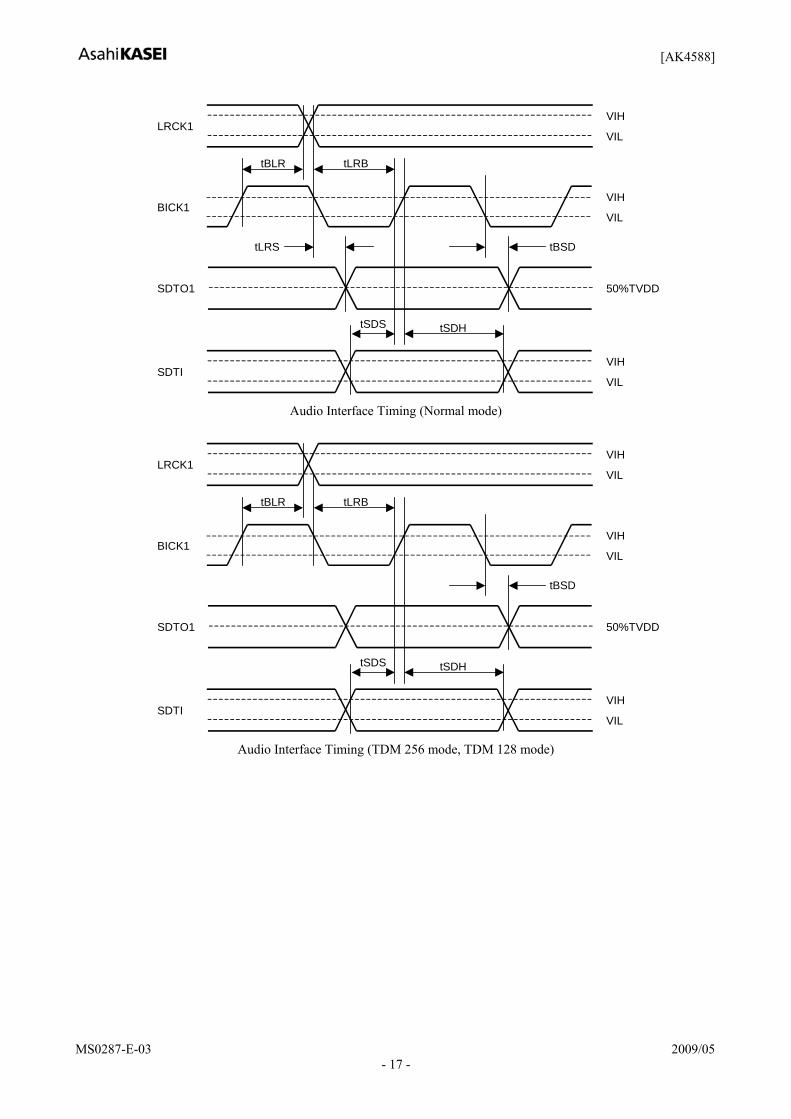
Parameter Symbol min typ max Units Audio Interface Timing (Slave Mode) Normal mode
BICK1 Period BICK1 Pulse Width Low
Pulse Width High LRCK1 Edge to BICK1 “↑” (Note 18) BICK1 “↑” to LRCK1 Edge (Note 18) LRCK1 to SDTO1(MSB) BICK1 “↓” to SDTO1 SDTI1-4,DAUX1 Hold Time SDTI1-4,DAUX1 Setup Time
tBCK tBCKL tBCKH tLRB tBLR tLRS tBSD tSDH tSDS
81 32 32 20 20
20 20
40 40
ns ns ns ns ns ns ns ns ns
TDM 256 mode BICK1 Period BICK1 Pulse Width Low
Pulse Width High LRCK1 Edge to BICK1 “↑” (Note 18) BICK1 “↑” to LRCK1 Edge (Note 18) BICK1 “↓” to SDTO1 SDTI1 Hold Time SDTI1 Setup Time
tBCK tBCKL tBCKH tLRB tBLR tBSD tSDH tSDS
81 32 32 20 20
10 10
20
ns ns ns ns ns ns ns ns
TDM 128 mode BICK1 Period BICK1 Pulse Width Low
Pulse Width High LRCK1 Edge to BICK1 “↑” (Note 18) BICK1 “↑” to LRCK1 Edge (Note 18) BICK1 “↓” to SDTO1 SDTI1-2 Hold Time SDTI1-2 Setup Time
tBCK tBCKL tBCKH tLRB tBLR tBSD tSDH tSDS
81 32 32 20 20
10 10
20
ns ns ns ns ns ns ns ns
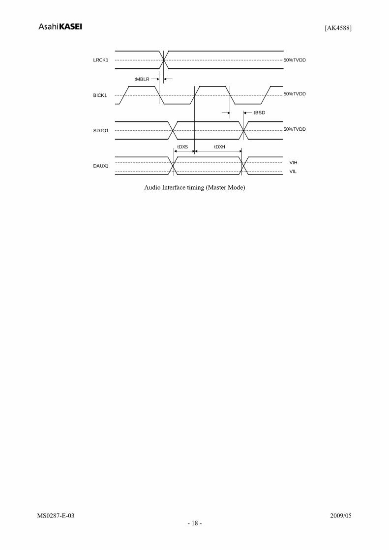
Audio Interface Timing (Master Mode) Normal mode
BICK1 Frequency BICK1 Duty BICK1 “↓” to LRCK1 Edge BICK1“↓” to SDTO1 SDTI1-4,DAUX1 Hold Time SDTI1-4,DAUX1 setup Time
fBCK dBCK tMBLR tBSD tSDH tSDS
-20
20 20
64fs 50
20 40
Hz % ns ns ns ns
TDM 256 mode BICK1 Frequency BICK1 Duty (Note 19) BICK1 “↓” to LRCK1 Edge BICK1 “↓” to SDTO1 SDTI1 Hold Time SDTI1 Setup Time
fBCK dBCK tMBLR tBSD tSDH tSDS
-12
10 10
256fs
50
12 20
Hz % ns ns ns ns
TDM 128 mode BICK1 Frequency BICK1 Duty (Note 20) BICK1 “↓” to LRCK1 Edge BICK1 “↓” to SDTO1 SDTI1-2 Hold Time SDTI1-2 Setup Time
fBCK dBCK tMBLR tBSD tSDH tSDS
-12
10 10
128fs
50
12 20
Hz % ns ns ns ns
Note 18. BICK1 rising edge must not occur at the same time as LRCK1 edge. Note 19. When MCLK is 512fs, dBCK is guaranteed. When 384fs and 256fs, dBCK can not be guaranteed. Note 20. When MCLK is 256fs, dBCK is guaranteed. When 128fs, dBCK can not be guaranteed.

[AK4588]
MS0287-E-03 2009/05 - 16 -
■ Timing Diagram(ADC/DAC part) 1/fCLK
tCLKL
VIH
tCLKH
MCLKVIL
1/fsn, 1/fsd, 1/fsq
LRCK1 VIH
VIL
tBCK
tBCKL
VIH
tBCKH
BICK1 VIL
Clock Timing (Normal mode)
1/fCLK
tCLKL
VIH
tCLKH
MCLKVIL
1/fs
LRCK1 VIH
VIL
tLRLtLRH
tBCK
tBCKL
VIH
tBCKH
BICK1 VIL
Clock Timing (TDM 256 mode, TDM 128 mode)
[AK4588]
MS0287-E-03 2009/05 - 17 -
tLRB
LRCK1
VIH BICK1
VIL
tLRS
SDTO1 50%TVDD
tBSD
VIH
VIL
tBLR
tSDS
SDTI VIH
VIL
tSDH
Audio Interface Timing (Normal mode)
tLRB
LRCK1
VIH BICK1
VIL
SDTO1 50%TVDD
tBSD
VIH
VIL
tBLR
tSDS
SDTI VIH
VIL
tSDH
Audio Interface Timing (TDM 256 mode, TDM 128 mode)
[AK4588]
MS0287-E-03 2009/05 - 18 -
LRCK1
BICK1
SDTO1
tBSD
tMBLR
50%TVDD
50%TVDD
50%TVDD
DAUX1
tDXHtDXS
VIH
VIL
Audio Interface timing (Master Mode)
[AK4588]
MS0287-E-03 2009/05 - 19 -
SWITCHING CHARACTERISTICS (DIR/DIT part)
(Ta=25°C; DVDD=AVDD4.5~5.5V, TVDD=2.7~5.5V; CL=20pF) Parameter Symbol min typ max Units
Master Clock Timing Crystal Resonator Frequency fXTAL 11.2896 24.576 MHz External Clock Frequency
Duty fECLK dECLK
11.289640
50
24.576 60
MHz %
MCKO1 Output Frequency Duty
fMCK1 dMCK1
4.096 40
50
24.576 60
MHz %
MCKO2 Output Frequency Duty
fMCK2 dMCK2
2.048 40
50
24.576 60
MHz %
PLL Clock Recover Frequency (RX0-7) fpll 32 - 192 kHz LRCK2 Frequency
Duty Cycle fs
dLCK 32 45
192 55
kHz %
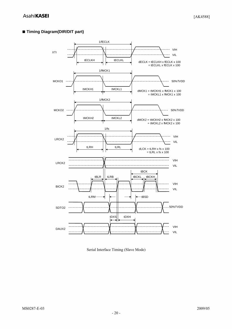
Audio Interface Timing Slave Mode BICK2 Period BICK2 Pulse Width Low
Pulse Width High LRCK2 Edge to BICK2 “↑” (Note 21) BICK2 “↑” to LRCK2 Edge (Note 21) LRCK2 to SDTO2 (MSB) BICK2 “↓” to SDTO2 DAUX2 Hold Time DAUX2 Setup Time
tBCK
tBCKL tBCKH tLRB tBLR tLRM tBSD tDXH tDXS
80 30 30 20 20
20 20
30 30
ns ns ns ns ns ns ns ns ns
Master Mode BICK2 Frequency BICK2 Duty BICK2 “↓” to LRCK2 BICK2 “↓” to SDTO2 DAUX2 Hold Time DAUX2 Setup Time
fBCK dBCK
tMBLR tBSD tDXH tDXS
-20
20 20
64fs 50
20 15
Hz % ns ns ns ns
Note 21. BICK2 rising edge must not occur at the same time as LRCK2 edge.
[AK4588]
MS0287-E-03 2009/05 - 20 -
■ Timing Diagram(DIR/DIT part)
1/fECLK
tECLKL
VIH
tECLKH
XTIVIL
dECLK = tECLKH x fECLK x 100= tECLKL x fECLK x 100
1/fMCK1
50%TVDD MCKO1
tMCKL1tMCKH1 dMCK1 = tMCKH1 x fMCK1 x 100 = tMCKL1 x fMCK1 x 100
1/fMCK2
50%TVDD MCKO2
tMCKL2tMCKH2 dMCK2 = tMCKH2 x fMCK2 x 100 = tMCKL2 x fMCK2 x 100
1/fs
LRCK2 VIH
VIL
tLRLtLRH dLCK = tLRH x fs x 100 = tLRL x fs x 100
tLRB
LRCK2
BICK2
SDTO2
tBSD
tBLR tBCKL tBCKH
tLRM
50%TVDD
DAUX2
tDXS tDXH
VIH
VIL
VIH
VIL
VIH
VIL
tBCK
Serial Interface Timing (Slave Mode)

[AK4588]
MS0287-E-03 2009/05 - 21 -
LRCK2
BICK2
SDTO2
tBSD
tMBLR
50%TVDD
50%TVDD
50%TVDD
DAUX2
tDXHtDXS
VIH
VIL
Serial Interface Timing (Master Mode)
tPD
PDN VIL
Power Down & Reset Timing
[AK4588]
MS0287-E-03 2009/05 - 22 -
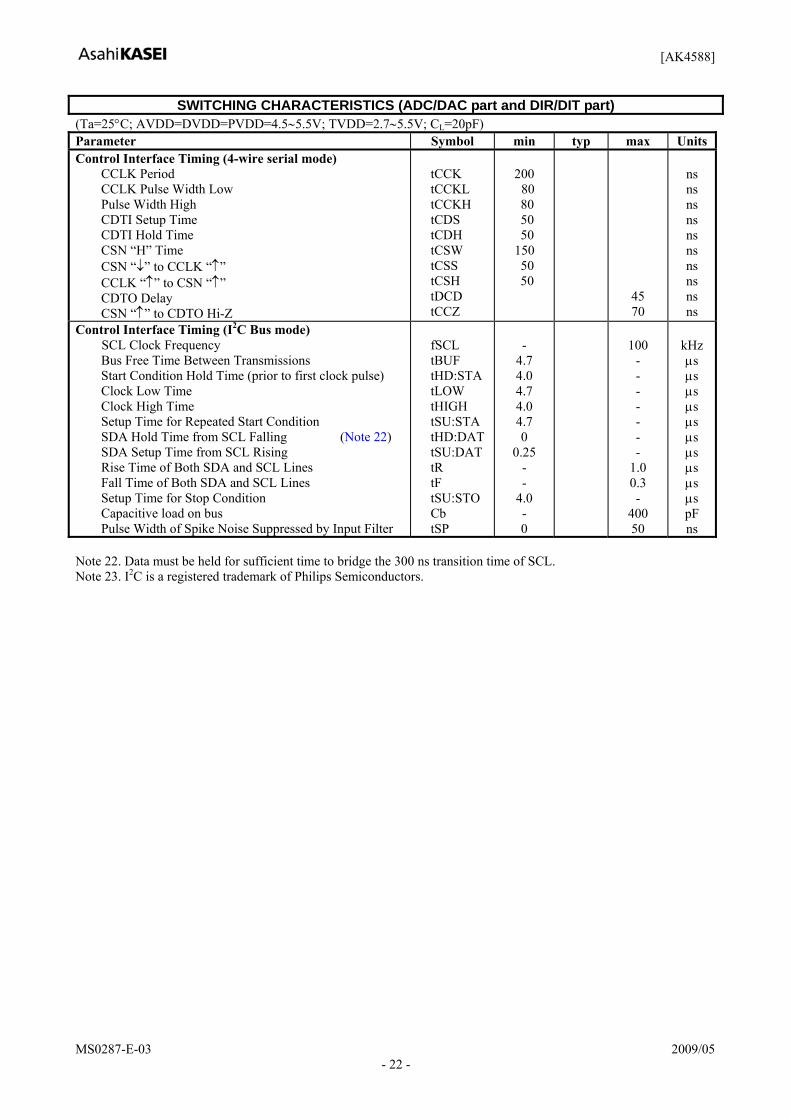
SWITCHING CHARACTERISTICS (ADC/DAC part and DIR/DIT part) (Ta=25°C; AVDD=DVDD=PVDD=4.5∼5.5V; TVDD=2.7∼5.5V; CL=20pF) Parameter Symbol min typ max UnitsControl Interface Timing (4-wire serial mode)
CCLK Period CCLK Pulse Width Low Pulse Width High CDTI Setup Time CDTI Hold Time CSN “H” Time CSN “↓” to CCLK “↑” CCLK “↑” to CSN “↑” CDTO Delay CSN “↑” to CDTO Hi-Z
tCCK tCCKL tCCKH tCDS tCDH tCSW tCSS tCSH
tDCD tCCZ
200
80 80 50 50
150 50 50
45 70
ns ns ns ns ns ns ns ns ns ns
Control Interface Timing (I2C Bus mode) SCL Clock Frequency Bus Free Time Between Transmissions Start Condition Hold Time (prior to first clock pulse) Clock Low Time Clock High Time Setup Time for Repeated Start Condition SDA Hold Time from SCL Falling (Note 22) SDA Setup Time from SCL Rising Rise Time of Both SDA and SCL Lines Fall Time of Both SDA and SCL Lines Setup Time for Stop Condition Capacitive load on bus Pulse Width of Spike Noise Suppressed by Input Filter
fSCL tBUF tHD:STA tLOW tHIGH tSU:STA tHD:DAT tSU:DAT tR tF tSU:STO Cb tSP
-
4.7 4.0 4.7 4.0 4.7 0
0.25 - -
4.0 - 0
100
- - - - - - -
1.0 0.3 -
400 50
kHzμs μs μs μs μs μs μs μs μs μs pF ns
Note 22. Data must be held for sufficient time to bridge the 300 ns transition time of SCL. Note 23. I2C is a registered trademark of Philips Semiconductors.

[AK4588]
MS0287-E-03 2009/05 - 23 -
■ Timing Diagram (ADC/DAC part and DIR/DIT part)
tCCKL
CSN
CCLK
tCDS
CDTI
tCDH
tCSS
C0 A4
tCCKH
CDTO Hi-Z
R/WC1
VIH
VIL
VIH
VIL
VIH
VIL
tCCK
WRITE/READ Command Input Timing in 4-wire serial mode The ADC/DAC part doesn’t support READ command.
tCSW
CSN
CCLK
CDTI D2 D0
tCSH
CDTO Hi-Z
D1D3
VIH
VIL
VIH
VIL
VIH
VIL
WRITE Data Input Timing in 4-wire serial mode
CSN
CCLK
tDCD
CDTO D7 D6
CDTI A1 A0
D5 Hi-Z 50%TVDD
VIH
VIL
VIH
VIL
VIH
VIL
READ Data Output Timing 1 in 4-wire serial mode
The ADC/DAC part doesn’t support READ command..

[AK4588]
MS0287-E-03 2009/05 - 24 -
CSN
CCLK
tCCZ
CDTO D2 D1
CDTI
D0 D3
tCSW
tCSH
50%TVDD
VIH
VIL
VIH
VIL
VIH
VIL
READ Data Input Timing 2 in 4-wire serial mode
The ADC/DAC part doesn’t support READ command.
tHIGH
SCL
SDAVIH
tLOWtBUF
tHD:STA
tR tF
tHD:DAT tSU:DAT tSU:STA
Stop Start Start Stop
tSU:STO
VIL
VIH
VIL
tSP
I2C Bus mode Timing
The ADC/DAC part doesn’t support READ command.
tPD
VILPDN
tPDV
SDTO 50%TVDD
VIH
Power-down & Reset Timing

[AK4588]
MS0287-E-03 2009/05 - 25 -
OPERATION OVERVIEW (ADC/DAC part) ■ System Clock The external clocks, which are required to operate the AK4588, are MCLK, LRCK1 and BICK1. MCLK should be synchronized with LRCK1 but the phase is not critical. There are two methods to set MCLK frequency. In Manual Setting Mode (ACKS bit = “0”: Default), the sampling speed is set by DFS1-0 bit (Table 1). The frequency of MCLK at each sampling speed is set automatically. (Table 3, Table 4, Table 5) In Auto Setting Mode (ACKS bit = “1”), as MCLK frequency is detected automatically (Table 6) and the internal master clock becomes the appropriate frequency (Table 7), it is not necessary to set DFS1-0 bits. Only MCLK is necessary in the master mode. Master Clock Input Frequency should be selected by CKS1-0 bits (Table 2), and Sampling Speed should be selected by DFS1-0 bits (Table 1). The frequencies and the duties of the clocks (LRCK1, BICK1) may not be stabile after setting CKS1-0 bits and DFS1-0 bits up. External clocks (MCLK, BICK1, LRCK1) should always be present whenever the AK4588 is in normal operation mode (PDN pin = “H”). If these clocks are not provided, the AK4588 may draw excess current because the device utilizes dynamic refreshed logic internally. If the external clocks are not present, the AK4588 should be in the power-down mode (PDN pin = “L”) or in the reset mode (RSTN1 bit = “0”). After exiting reset at power-up etc., the AK4588 is in the power-down mode until MCLK and LRCK are input. In the Master mode, External clock(MCLK) should always be supplied except in the power-down mode. It is in power-down mode until MCLK will be supplied, when Reset was canceled by Power-ON and so on.
DFS1 DFS0 Sampling Speed (fs) 0 0 Normal Speed Mode 32kHz~48kHz 0 1 Double Speed Mode 64kHz~96kHz
(default)
1 0 Quad Speed Mode 120kHz~192kHz
Table 1. Sampling Speed (Manual Setting Mode)
CKS1 CKS0 Normal Double Quad 0 0 256fs 128fs 128fs (default)0 1 384fs 192fs 128fs 1 0 512fs 256fs 128fs 1 1 256fs 256fs 128fs
Table 2.Master clock input select (Master Mode)
LRCK1 MCLK (MHz) BICK1 (MHz)
Fs 256fs 384fs 512fs 64fs 32.0kHz 8.1920 12.2880 16.3840 2.0480 44.1kHz 11.2896 16.9344 22.5792 2.8224 48.0kHz 12.2880 18.4320 24.5760 3.0720
Table 3. System Clock Example (Normal Speed Mode @Manual Setting Mode)
LRCK1 MCLK (MHz) BICK1 (MHz) Fs 128fs 192fs 256fs 64fs
88.2kHz 11.2896 16.9344 22.5792 5.6448 96.0kHz 12.2880 18.4320 24.5760 6.1440
Table 4. System Clock Example (Double Speed Mode @Manual Setting Mode)
(Note: At Double speed mode (DFS1= “0”, DFS0 = “1”), 128fs and 192fs are not available for ADC.)

[AK4588]
MS0287-E-03 2009/05 - 26 -
LRCK1 MCLK (MHz) BICK1 (MHz) Fs 128fs 192fs 256fs 64fs
176.4kHz 22.5792 - - 11.2896 192.0kHz 24.5760 - - 12.2880
Table 5. System Clock Example (Quad Speed Mode @Manual Setting Mode)
(Note: At Quad speed mode (DFS1= “1”, DFS0 = “0”) are not available for ADC.)
MCLK Sampling Speed512fs Normal 256fs Double 128fs Quad
Table 6. Sampling Speed (Auto Setting Mode)
LRCK1 MCLK (MHz) fs 128fs 256fs 512fs
Sampling Speed
32.0kHz - - 16.3840 44.1kHz - - 22.5792 48.0kHz - - 24.5760
Normal
88.2kHz - 22.5792 - 96.0kHz - 24.5760 - Double
176.4kHz 22.5792 - - 192.0kHz 24.5760 - - Quad
Table 7. System Clock Example (Auto Setting Mode)
■ De-emphasis Filter The AK4588 includes the digital de-emphasis filter (tc=50/15μs) by IIR filter. De-emphasis filter is not available in Double Speed Mode and Quad Speed Mode. This filter corresponds to three sampling frequencies (32kHz, 44.1kHz, 48kHz). De-emphasis of each DAC can be set individually by register data of DEMA1-C0 bits (DAC1: DEMA1-0 bits, DAC2: DEMB1-0 bits, DAC3: DEMC1-0 bits, DAC4: DEMD1-0 bits, see “Register Definitions”).
Mode Sampling Speed DEM1 DEM0 DEM
0 Normal Speed 0 0 44.1kHz 1 Normal Speed 0 1 OFF 2 Normal Speed 1 0 48kHz 3 Normal Speed 1 1 32kHz
(default)
Table 8. De-emphasis control
■ Digital High Pass Filter The ADC has a digital high pass filter for DC offset cancel. The cut-off frequency of the HPF is 1.0Hz at fs=48kHz and scales with sampling rate (fs).

[AK4588]
MS0287-E-03 2009/05 - 27 -
■ Master mode and Slave mode Master Mode can be selected by setting the MASTER pin to “H”. LRCK1 and BICK1 will be outputs in Master Mode. And, Slave Mode can be selected by setting this pin to “L”. LRCK1 and BICK1 will be inputs in Slave Mode. Operation of LRCK1 and BICK1 is shown below Table 9.
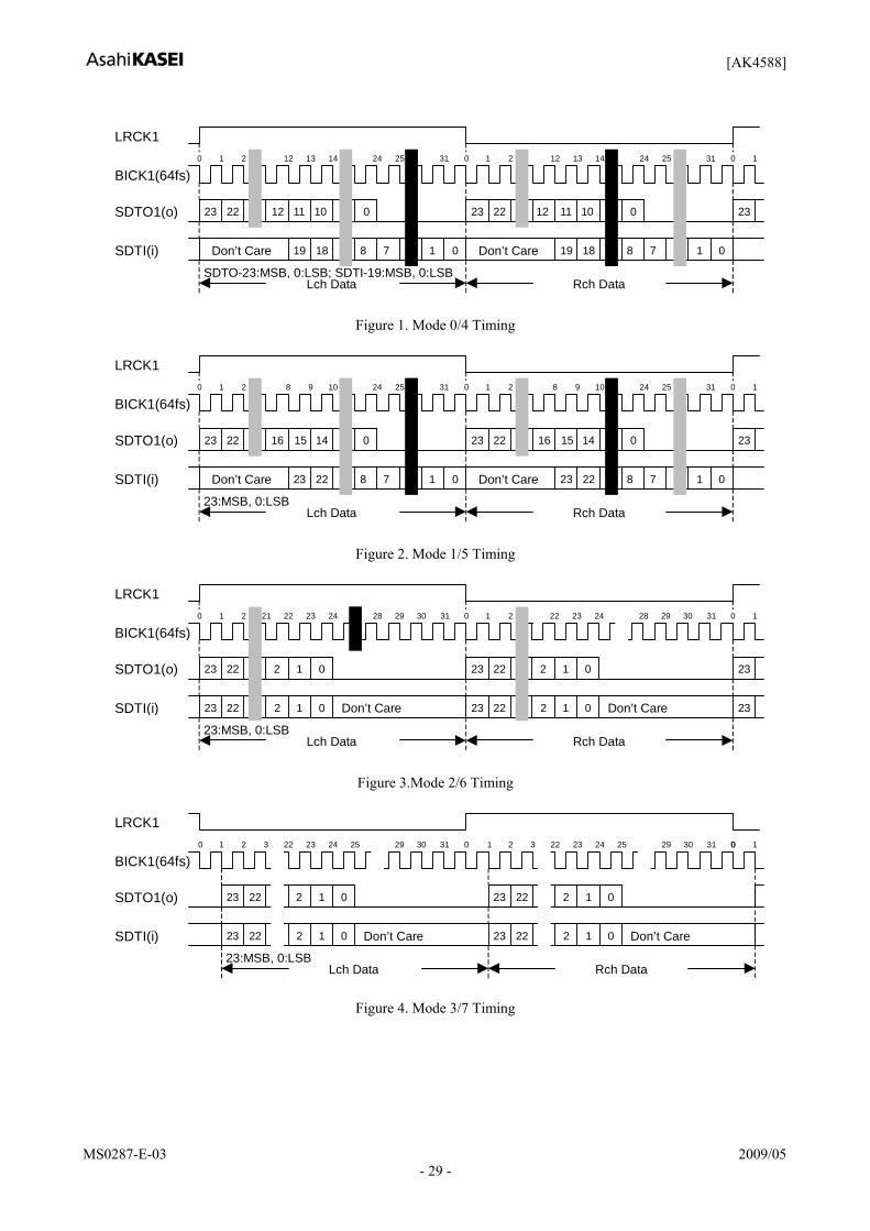
Table 9. Operation of LRCK1 and BICK1 ■ Audio Serial Interface Format When TDM1-0 bit = “00”, 8 modes can be selected by the DIF1-0 bits as shown in Table 10. In all modes the serial data is MSB-first, 2’s complement format. The SDTO1 is clocked out on the falling edge of BICK1 and the SDTI/DAUX1 are latched on the rising edge of BICK1. Figure 1∼Figure 4 shows the timing at SDOS bit = “0”. In this case, the SDTO1 outputs the ADC output data. When SDOS bits = “1”, the data input to DAUX1 is converted to SDTO1’s format and output from SDTO1. Mode 2/3/6/7/10/11/14/15/18/19/22/23 in SDTI input formats can be used for 16-20bit data by zeroing the unused LSBs.
LRCK1 BICK1 Mode MASTER TDM 1 TDM0 DIF1 DIF0 SDTO1 SDTI1-4, DAUX1 I/O I/O
0 0 0 0 0 0 24bit, Left justified
20bit, Right justified H/L I ≥ 48fs I
1 0 0 0 0 1 24bit, Left justified
24bit, Right justified H/L I ≥ 48fs I
2 0 0 0 1 0 24bit, Left justified
24bit, Left justified H/L I ≥ 48fs I (default)
3 0 0 0 1 1 24bit, I2S 24bit, I2S L/H I ≥ 48fs I
4 1 0 0 0 0 24bit, Left justified
20bit, Right justified H/L O 64fs O
5 1 0 0 0 1 24bit, Left justified
24bit, Right justified H/L O 64fs O
6 1 0 0 1 0 24bit, Left justified
24bit, Left justified H/L O 64fs O
7 1 0 0 1 1 24bit, I2S 24bit, I2S L/H O 64fs O
Table 10. Audio data formats (Normal mode) The audio serial interface format becomes the TDM 256 mode if TDM1-0 bits are set to “01”. In the TDM 256 Mode, the serial data of all DAC (eight channels) is input to the SDTI1 pin. The input data to SDTI2-4 pins is ignored. BICK1 should be fixed to 256fs. “H” time and “L” time of LRCK1 pin should be 1/256fs at least. Eight modes can be selected by the DIF1-0 bits was shown in Table 11. In all modes the serial data is MSB-first, 2’s complement format. The SDTO1 pin is clocked out on the falling edge of BICK1 pin and the SDTI1 pin are latched on the rising edge of BICK1 pin. SDOS bit and LOOP1-0 bits should be set to “0” in the TDM mode. TDM 128 Mode can be set by TDM1-0 bit = “10”. In this Mode, the serial data of DAC (four channels; L1, R1, L2, R2) is input to the SDTI1 pin. Other four data (L3, R3, L4, R4) are input to the SDTI2 pin.
PDN pin PWADN bit, PWDAN bit MASTER pin LRCK1 pin BICK1 pin L Input Input L -- H “L” output “L” output L Input Input H “00” H “L” output “L” output L Input Input H Except for “00” H Output Output

[AK4588]
MS0287-E-03 2009/05 - 28 -
LRCK1 BICK1 Mode MASTER TDM 1 TDM0 DIF1 DIF0 SDTO1 SDTI1 I/O I/O
8 0 0 1 0 0 24bit, Left justified
20bit, Right justified ↑ I 256fs I
9 0 0 1 0 1 24bit, Left justified
24bit, Right justified ↑ I 256fs I
10 0 0 1 1 0 24bit, Left justified
24bit, Left justified ↑ I 256fs I
11 0 0 1 1 1 24bit, I2S 24bit, I2S ↓ I 256fs I
12 1 0 1 0 0 24bit, Left justified
20bit, Right justified ↑ O 256fs O
13 1 0 1 0 1 24bit, Left justified
24bit, Right justified ↑ O 256fs O
14 1 0 1 1 0 24bit, Left justified
24bit, Left justified ↑ O 256fs O
15 1 0 1 1 1 24bit, I2S 24bit, I2S ↓ O 256fs O
Table 11. Audio data formats (TDM 256 mode)
LRCK1 BICK1 Mode MASTER TDM 1 TDM0
DIF1 DIF0 SDTO1 SDTI1, SDTI2 I/O I/O
16 0 1 1 0 0 24bit, Left justified
20bit, Right justified ↑ I 128fs I
17 0 1 1 0 1 24bit, Left justified
24bit, Right justified ↑ I 128fs I
18 0 1 1 1 0 24bit, Left justified
24bit, Left justified ↑ I 128fs I
19 0 1 1 1 1 24bit, I2S 24bit, I2S ↓ I 128fs I
20 1 1 1 0 0 24bit, Left justified
20bit, Right justified ↑ O 128fs O
21 1 1 1 0 1 24bit, Left justified
24bit, Right justified ↑ O 128fs O
22 1 1 1 1 0 24bit, Left justified
24bit, Left justified ↑ O 128fs O
23 1 1 1 1 1 24bit, I2S 24bit, I2S ↓ O 128fs O
Table 12. Audio data formats (TDM 128 mode)
[AK4588]
MS0287-E-03 2009/05 - 29 -
LRCK1
BICK1(64fs)
SDTO1(o)
0 1 2 12 13 14 24 25 31 0 1 2 12 13 14 24 25 31 0
23
1
22 0 23 22 12 11 10 0 23
SDTI(i) 118 019 8 7 1 18 019 8 7
Lch Data Rch Data
Don’t Care Don’t Care
12 11 10
SDTO-23:MSB, 0:LSB; SDTI-19:MSB, 0:LSB
Figure 1. Mode 0/4 Timing
LRCK1
BICK1(64fs)
SDTO1(o)
0 1 2 8 9 10 24 25 31 0 1 2 8 9 10 24 25 31 0
23
1
22 0 23 22 16 15 14 0 23
SDTI(i) 122 023 8 7 1 22 023 8 7
23:MSB, 0:LSB Lch Data Rch Data
Don’t Care Don’t Care
16 15 14
Figure 2. Mode 1/5 Timing
LRCK1
BICK1(64fs)
SDTO1(o)
0 1 2 21 22 23 24 31 0 1 2 0
23
1
22 1 23 22 23
SDTI(i) 22 23 0 2223
23:MSB, 0:LSB Lch Data Rch Data
Don’t Care
2
2 1
28 29 30
23
0
22 23 24 31
1
0 Don’t Care
2
2 1
28 29 30
0
Figure 3.Mode 2/6 Timing
LRCK1
BICK1(64fs)
SDTO1(o)
0 1 2 3 22 23 24 25 0 0 1
SDTI(i)
3129 30
23 22 1
2223 0
23:MSB, 0:LSB Lch Data Rch Data
Don’t Care
2
2 1
0
2 3 22 23 24 25 031 29 30
23 22 1
2223 0 Don’t Care
2
2 1
0
1
Figure 4. Mode 3/7 Timing

[AK4588]
MS0287-E-03 2009/05 - 30 -
256 BICK
BICK1(256fs)
SDTO1(o)
SDTI1(i)
22 0
Lch 32 BICK
18 0
L1 32 BICK
18 0
R1 32 BICK
18 0
L2 32 BICK
18 0
R2 32 BICK
18 0
L3 32 BICK
18 0
R3 32 BICK
18 0
L4 32 BICK
18 0
R4 32 BICK
22 0
Rch 32 BICK
22 23
19 19 19 19 19
23
19 19 19
23
19
LRCK1
LRCK1 (mode 8)
(mode 12)
Figure 5. Mode 8/12 Timing
256 BICK
BICK1(256fs)
SDTO1(o)
SDTI1(i)
22 0
Lch 32 BICK
22 0
L1 32 BICK
22 0
R1 32 BICK
22 0
L2 32 BICK
22 0
R2 32 BICK
22 0
L3 32 BICK
22 0
R3 32 BICK
22 0
L4 32 BICK
22 0
R4 32 BICK
22 0
Rch 32 BICK
22 23
23 23 23 23 23
23
23 23 23
23
23
LRCK1
LRCK1 (mode 9)
(mode 13)
Figure 6. Mode 9/13 Timing
256 BICK
BICK1(256fs)
SDTO1(o)
SDTI1(i)
22 0
Lch 32 BICK
22 0
L1 32 BICK
22 0
R1 32 BICK
22 0
L2 32 BICK
22 0
R2 32 BICK
22 0
L3 32 BICK
22 0
R3 32 BICK
22 0
L4 32 BICK
22 0
R4 32 BICK
22 0
Rch 32 BICK
22
22
23
23 23 23 23 23
23
23 23 23
23
23
LRCK1
LRCK1 (mode 10)
(mode 14)
Figure 7. Mode 10/14 Timing
256 BICK
BICK1(256fs)
SDTO1(o)
SDTI1(i)
23 0
Lch 32 BICK
23 0
L1 32 BICK
23 0
R1 32 BICK
23 0
L2 32 BICK
23 0
R2 32 BICK
23 0
L3 32 BICK
23 0
R3 32 BICK
23 0
L4 32 BICK
23 0
R4 32 BICK
23 0
Rch 32 BICK
23
23
LRCK1
LRCK1 (mode 11)
(mode 15)
Figure 8. Mode 11/15 Timing

[AK4588]
MS0287-E-03 2009/05 - 31 -
128 BICK
BICK1(128fs)
SDTO1(o) 22 0
Lch 32 BICK
L1 32 BICK
R1 32 BICK
L2 32 BICK
R2 32 BICK
L3 32 BICK
R3 32 BICK
L4 32 BICK
R4 32 BICK
22 0
Rch 32 BICK
22 23 23 23
SDTI1(i) 18 0 18 0 18 0 18 0 19 19 19 19 19
LRCK1
SDTI2(i) 18 0 18 0 18 0 18 0 19 19 19 19 19
LRCK1 (mode 16)
(mode 20)
Figure 9. Mode 16/20 Timing
128 BICK
BICK1(128fs)
(mode 17)
22 0
Lch 32 BICK
L1 32 BICK
R1 32 BICK
L2 32 BICK
R2 32 BICK
L3 32 BICK
R3 32 BICK
L4 32 BICK
R4 32 BICK
22 0
Rch 32 BICK
22 23 23 23
SDTI1(i) 22 0 22 0 22 0 22 0 23 23 23 23 19
LRCK1
SDTI2(i) 22 0 22 0 22 0 22 0 23 23 23 23 19
LRCK1 (mode 21)
Figure 10. Mode 17/21 Timing
128 BICK
BICK1(128fs)
SDTO1(o) 22 0
Lch 32 BICK
L1 32 BICK
R1 32 BICK
L2 32 BICK
R2 32 BICK
L3 32 BICK
R3 32 BICK
L4 32 BICK
R4 32 BICK
22 0
Rch 32 BICK
22 23 23 23
LRCK1
SDTI1(i) 22 0 22 0 22 0 22 0 23 23 23 23 22 23
SDTI2(i) 22 0 22 0 22 0 22 0 23 23 23 23 22 23
LRCK1
(mode 18)
(mode 22)
Figure 11. Mode 18/22 Timing

[AK4588]
MS0287-E-03 2009/05 - 32 -
128 BICK
BICK1(128fs)
SDTO1(o) 22 0
Lch 32 BICK
L1 32 BICK
R1 32 BICK
L2 32 BICK
R2 32 BICK
L3 32 BICK
R3 32 BICK
L4 32 BICK
R4 32 BICK
22 0
Rch 32 BICK
23 23 23
SDTI1(i) 22 0 22 0 22 0 22 0 23 23 23 23 23
SDTI2(i) 22 0 22 0 22 0 22 0 23 23 23 23 23
LRCK1
LRCK1 (mode 19)
(mode 23)
Figure 12. Mode 19/23 Timing

[AK4588]
MS0287-E-03 2009/05 - 33 -
■ Overflow Detection The AK4588 has overflow detect function for the analog input. Overflow detect function is enable if OVFE bit is set to “1”. The OVF pin goes to “H” if analog input of Lch or Rch overflows (more than -0.3dBFS). OVF output for overflowed analog input has the same group delay as ADC (GD = 19.1/fs = 398μs @fs=48kHz). The OVF pin is “L” for 522/fs (=11.8ms @fs=48kHz) after PDN = “↑”, and then overflow detection is enabled. ■ Zero Detection The AK4588 has two pins for zero detect flag outputs. Channel grouping can be selected by DZFM3-0 bits (Table 13). The DZF1 pin corresponds to the group 1 channels and the DZF2 pin corresponds to the group 2 channels. However the DZF2 pin becomes the OVF pin if OVFE bit is set to “1”. Zero detection mode is set to mode 0. DZF1 is AND of all eight channels and DZF2 is disabled (“L”) at mode 0. Table 14 shows the relation of OVFE bit and DZF. When the input data of all channels in the group 1(group 2) are continuously zeros for 8192 LRCK1 cycles, DZF1 (DZF2) pin goes to “H”. DZF1 (DZF2) pin immediately returns to “L” if input data of any channels in the group 1 (group 2) is not zero after going DZF1 (DZF2) “H”.
DZFM AOUT Mode 3 2 1 0 L1 R1 L2 R2 L3 R3 L4 R4 0 0 0 0 0 DZF1 DZF1 DZF1 DZF1 DZF1 DZF1 DZF1 DZF1 1 0 0 0 1 DZF1 DZF1 DZF1 DZF1 DZF1 DZF2 DZF2 DZF2 2 0 0 1 0 DZF1 DZF1 DZF1 DZF1 DZF2 DZF2 DZF2 DZF2 3 0 0 1 1 DZF1 DZF1 DZF1 DZF2 DZF2 DZF2 DZF2 DZF2 4 0 1 0 0 DZF1 DZF1 DZF2 DZF2 DZF2 DZF2 DZF2 DZF2 5 0 1 0 1 DZF1 DZF2 DZF2 DZF2 DZF2 DZF2 DZF2 DZF2 6 0 1 1 0 DZF2 DZF2 DZF2 DZF2 DZF2 DZF2 DZF2 DZF2 7 0 1 1 1 disable (DZF1=DZF2 = “L”) 8 1 0 0 0 DZF1 DZF1 DZF1 DZF1 DZF1 DZF1 DZF1 DZF2 9 1 0 0 1 DZF1 DZF1 DZF1 DZF1 DZF1 DZF1 DZF2 DZF2
10 1 0 1 0 11 1 0 1 1 12 1 1 0 0 13 1 1 0 1 14 1 1 1 0 15 1 1 1 1
disable (DZF1=DZF2 = “L”)
(default)
Table 13. Zero detect control
OVFE bit DZF1 pin DZF2/OVF pin
0 Selectable (Table 13) Selectable (Table 13) 1 Selectable (Table 13) OVF output
Table 14. DZF1-2 pins outputs

[AK4588]
MS0287-E-03 2009/05 - 34 -
■ Digital Attenuator The AK4588 has channel-independent digital attenuator (128 levels, 0.5dB step). Attenuation level of each channel can be set by each ATT7-0 bits (Table 15).
ATT7-0 Attenuation Level 00H 0dB 01H -0.5dB 02H -1.0dB
: : 7DH -62.5dB 7EH -63dB 7FH MUTE (-∞)
: FEH MUTE (-∞) FFH MUTE (-∞)
(default)
Table 15. Attenuation level of digital attenuator
Transition time between set values of ATT7-0 bits can be selected by ATS1-0 bits (Table 16). Transition between set values is the soft transition. Therefore, the switching noise does not occur in the transition.
Mode ATS1 ATS0 ATT speed 0 0 0 1792/fs 1 0 1 896/fs 2 1 0 256/fs 3 1 1 256/fs
(default)
Table 16. Transition time between set values of ATT7-0 bits
The transition between set values is soft transition of 1792 levels in mode 0. It takes 1792/fs (37.3ms@fs=48kHz) from 00H(0dB) to 7FH(MUTE) in mode 0. If the PDN pin goes to “L”, the ATTs are initialized to 00H. The ATTs are 00H when RSTN bit = “0”. When RSTN bit return to “1”, the ATTs fade to their current value.
[AK4588]
MS0287-E-03 2009/05 - 35 -
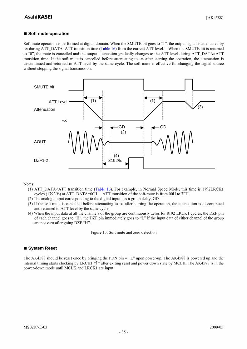
■ Soft mute operation Soft mute operation is performed at digital domain. When the SMUTE bit goes to “1”, the output signal is attenuated by -∞ during ATT_DATA×ATT transition time (Table 16) from the current ATT level. When the SMUTE bit is returned to “0”, the mute is cancelled and the output attenuation gradually changes to the ATT level during ATT_DATA×ATT transition time. If the soft mute is cancelled before attenuating to -∞ after starting the operation, the attenuation is discontinued and returned to ATT level by the same cycle. The soft mute is effective for changing the signal source without stopping the signal transmission.
SMUTE bit
Attenuation
DZF1,2
ATT Level
-∞
AOUT
8192/fs
GD GD
(1)
(2)
(3)
(4)
(1)
Notes:
(1) ATT_DATA×ATT transition time (Table 16). For example, in Normal Speed Mode, this time is 1792LRCK1 cycles (1792/fs) at ATT_DATA=00H. ATT transition of the soft-mute is from 00H to 7FH
(2) The analog output corresponding to the digital input has a group delay, GD. (3) If the soft mute is cancelled before attenuating to -∞ after starting the operation, the attenuation is discontinued
and returned to ATT level by the same cycle. (4) When the input data at all the channels of the group are continuously zeros for 8192 LRCK1 cycles, the DZF pin
of each channel goes to “H”. the DZF pin immediately goes to “L” if the input data of either channel of the group are not zero after going DZF “H”.
Figure 13. Soft mute and zero detection
■ System Reset The AK4588 should be reset once by bringing the PDN pin = “L” upon power-up. The AK4588 is powered up and the internal timing starts clocking by LRCK1 “↑” after exiting reset and power down state by MCLK. The AK4588 is in the power-down mode until MCLK and LRCK1 are input.

[AK4588]
MS0287-E-03 2009/05 - 36 -
■ Power ON/OFF Sequence
The ADC and DACs of the AK4588 are placed in the power-down mode by bringing the PDN pin “L” and both digital filters are reset at the same time. PDN pin “L” also reset the control registers to their default values. In the power-down mode, the analog outputs go to VCOM voltage and DZF1-2 pins go to “L”. This reset should always be executed after power-up. In case of the ADC, an analog initialization cycle starts after exiting the power-down mode. Therefore, the output data, SDTO1 becomes available after 522 cycles of LRCK1 clock. In case of the DAC, an analog initialization cycle starts after exiting the power-down mode. The analog outputs are VCOM voltage during the initialization. Figure 14 shows the sequences of the power-down and the power-up. The ADC and all DACs can be powered-down individually by PWADN and PWDAN bits. And DAC1-4 can be power-down individually by PD1-4 bits. In this case, the internal register values are not initialized. When PWADN bit = “0”, the SDTO1 pin goes to “L”. When PWDAN bit = “0” and PD1-4 bits = “0”, the analog outputs go to VCOM voltage and DZF1-2 pins go to “H”. Because some click noise occurs, the analog output should muted externally if the click noise influences system application.
ADC Internal State
PDN
Clock In MCLK,LRCK,SCLK
ADC In (Analog)
ADC Out (Digital)
DAC Internal State
DAC In (Digital)
DAC Out (Analog)
External Mute
Mute ON (9)
DZF1/DZF2
Power
Power-down
Don’t care
GD
“0”data
Power-down
“0”data
GD
(3)
(3)
(4)
(6)
(7)
(8)
522/fs
Init Cycle Normal Operation
(1)
GD
Normal Operation
GD
(5)
(6)
516/fs
Init Cycle
(2)
10∼11/fs (10)
Mute ON
“0”data
“0”data
Don’t care
Notes:
(1) The analog part of ADC is initialized after exiting the power-down state. (2) The analog part of DAC is initialized after exiting the power-down state. (3) Digital output corresponding to analog input and analog output corresponding to digital input have the group
delay (GD). (4) ADC output is “0” data at the power-down state. (5) Click noise occurs at the end of initialization of the analog part. Please mute the digital output externally if the
click noise influences system application. (6) Click noise occurs at the falling edge of PDN and at 512/fs after the rising edge of PDN. (7) When the external clocks (MCLK, BICK1 and LRCK1) are stopped, the AK4588 should be in the power-down
mode. (8) DZF1-2 pins are “L” in the power-down mode (PDN pin = “L”). (9) Please mute the analog output externally if the click noise (6) influences system application. (10) DZF= “L” for 10∼11/fs after PDN= “↑”.
Figure 14. Power-down/up sequence example

[AK4588]
MS0287-E-03 2009/05 - 37 -
■ Reset Function When RSTN1 bit = “0”, ADC and DACs are powered-down but the internal register are not initialized. The analog outputs go to VCOM voltage, DZF1-2 pins go to “H” and the SDTO1 pin goes to “L”. Because some click noise occurs, the analog output should muted externally if the click noise influences system application. Figure 15 shows the power-up sequence.
ADC Internal State
RSTN bit
Normal Operation Digital Block Power-down Normal Operation
Don’t care
GD GD
Clock InMCLK,LRCK,SCLK
ADC In (Analog)
“0”dataADC Out (Digital)
Normal Operation Normal OperationDAC Internal State
“0”dataDAC In (Digital)
DAC Out (Analog)
GD GD
(2)
(2)
(3)(4)
(6) (6)
DZF1/DZF2
(7)
InternalRSTN bit
Digital Block Power-down
1~2/fs (9)4~5/fs (9)
4∼5/fs (8)
(5)
516/fs
Init Cycle
(1)
Notes:
(1) The analog part of ADC is initialized after exiting the reset state. (2) Digital output corresponding to analog input and analog output corresponding to digital input have the group
delay (GD). (3) ADC output is “0” data at the power-down state. (4) Click noise occurs when the internal RSTN bit becomes “1”. Please mute the digital output externally if the click
noise influences system application. (5) When RSTN1 bit = “0”, the analog outputs go to VCOM voltage. (6) Click noise occurs at 4∼5/fs after RSTN1 bit becomes “0”, and occurs at 1∼2/fs after RSTN1 bit becomes “1”.
This noise is output even if “0” data is input. (7) The external clocks (MCLK, BICK1 and LRCK1) can be stopped in the reset mode. When exiting the reset
mode, “1” should be written to RSTN1 bit after the external clocks (MCLK, BICK1 and LRCK1) are fed. (8) DZF pins go to “H” when the RSTN1 bit becomes “0”, and go to “L” at 6~7/fs after RSTN1 bit becomes “1”. (9) There is a delay, 4~5/fs from RSTN1 bit “0” to the internal RSTN bit “0”.
Figure 15. Reset sequence example

[AK4588]
MS0287-E-03 2009/05 - 38 -
■ DAC partial Power-Down Function All DACs of The AK4588 can be powered-down individually by PD1-4 bits. The analog part of DAC is in power-down by PD1-4 bits = “1”, however, the digital part is not powered-down by it. Even if all DACs were set in power-down by the partial power-down bits, the digital part operation is continued. The analog output of the channel which is set in power-down by PD1-4 bits is fixed to VCOM voltage. And though DZF detection is being done, the result of DZF detection stops reflecting to DZF1-2 pins. Because some click noise occurs in both set-up and release of power-down, either the analog output should be muted externally or PD1-4 bits should be set up when it is in PWDAN bit = “0” or RSTN bit = “0”, if the click noise influences system application. Figure 16 shows the sequence of the power-down and the power-up by PD1-4 bits.
PD1-4 bit
DZF1/DZF2
8192/fs
“0”dataDAC In (Digital)
DAC Out (Analog)
GD GD (1)
(3) (3)(2)
DAC Digital Internal State
Normal Operation Normal Operation DAC Analog Internal State
Power-down
Normal Operation
Clock In MCLK,LRCK,SCLK
DAC In (Digital)
DAC Out (Analog)
Normal Operation Channel
(4)
(5)
GD
8192/fs
GD
Power-downNormal Operation Normal Operation
(2)(3) (3)
(4)
Power Down Channel
DZF Detect Internal State
DZF Detect Internal State
“0”data
(6)
Notes:
(1) Digital output corresponding to analog input and analog output corresponding to digital input have group delay (GD).
(2) Analog output of the DAC powered down by PD1-4 bits = “1” is fixed to the voltage of VCOM. (3) Immediately after PD1-4 bits are changed, some click noise occurs at the output of the channel changed by the
own PD bits. (4) Though DZF detection is being done at a certain channel which set up PD1-4 bits = “1”, the result of DZF
detection stops reflecting to DZF1-2 pins. (5) DZF detection of the DAC which is powered-down is ignored, and DZF1-2 pins go to “H”. (6) When the power-down function is set up and the channel has input signal, even if the partial power-down
function is set up, DZF1-2 pins will not be “H”.
Figure 16. DAC partial power-down example

[AK4588]
MS0287-E-03 2009/05 - 39 -
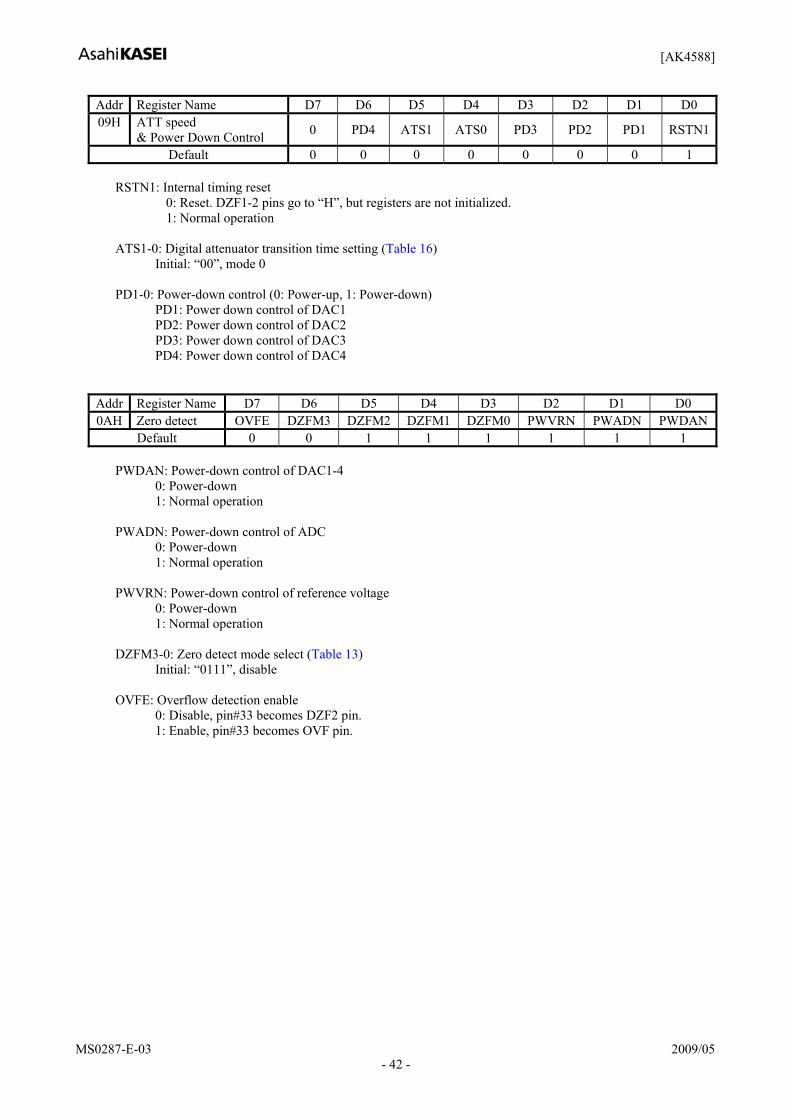
■ Register Map
Addr Register Name D7 D6 D5 D4 D3 D2 D1 D0 00H Control 1 0 0 TDM1 TDM0 DIF1 DIF0 0 SMUTE01H Control 2 CKS1 DFS1 LOOP1 LOOP0 SDOS DFS0 ACKS CKS0 02H LOUT1 Volume Control ATT7 ATT6 ATT5 ATT4 ATT3 ATT2 ATT1 ATT0 03H ROUT1 Volume Control ATT7 ATT6 ATT5 ATT4 ATT3 ATT2 ATT1 ATT0 04H LOUT2 Volume Control ATT7 ATT6 ATT5 ATT4 ATT3 ATT2 ATT1 ATT0 05H ROUT2 Volume Control ATT7 ATT6 ATT5 ATT4 ATT3 ATT2 ATT1 ATT0 06H LOUT3 Volume Control ATT7 ATT6 ATT5 ATT4 ATT3 ATT2 ATT1 ATT0 07H ROUT3 Volume Control ATT7 ATT6 ATT5 ATT4 ATT3 ATT2 ATT1 ATT0 08H De-emphasis DEMD1 DEMD0 DEMA1 DEMA0 DEMB1 DEMB0 DEMC1 DEMC009H ATT speed
& Power Down Control 0 PD4 ATS1 ATS0 PD3 PD2 PD1 RSTN1
0AH Zero detect OVFE DZFM3 DZFM2 DZFM1 DZFM0 PWVRN PWADN PWDAN0BH LOUT4 Volume Control ATT7 ATT6 ATT5 ATT4 ATT3 ATT2 ATT1 ATT0 0CH ROUT4 Volume Control ATT7 ATT6 ATT5 ATT4 ATT3 ATT2 ATT1 ATT0 Note: For addresses from 0DH to 1FH, data is not written.
When the PDN pin goes to “L”, the registers are initialized to their default values. When RSTN1 bit set to “0”, the internal timing is reset and the DZF1-2 pins go to “H”, but registers are not initialized to their default values.
■ Register Definitions
Addr Register Name D7 D6 D5 D4 D3 D2 D1 D0 00H Control 1 0 0 TDM1 TDM0 DIF1 DIF0 0 SMUTE
Default 0 0 0 0 1 0 0 0 SMUTE: Soft Mute Enable 0: Normal operation 1: All DAC outputs soft-muted
DIF1-0: Audio Data Interface Modes (Table 10) Initial: “10”, mode 2 TDM1-0: TDM Format Select (Table 11, Table 12)
Mode TDM1 TDM0 SDTI Sampling Speed 0 0 0 1-4 Normal, Double, Four Times Speed 1 0 1 1 Normal Speed 2 1 1 1-2 Double Speed

[AK4588]
MS0287-E-03 2009/05 - 40 -
Addr Register Name D7 D6 D5 D4 D3 D2 D1 D0 01H Control 2 CKS1 DFS1 LOOP1 LOOP0 SDOS DFS0 ACKS CKS0
Default 0 0 0 0 0 0 0 0
ACKS: Master Clock Frequency Auto Setting Mode Enable 0: Disable, Manual Setting Mode 1: Enable, Auto Setting Mode Master clock frequency is detected automatically at ACKS bit “1”. In this case, the setting of DFS1-0 bits are ignored. When this bit is “0”, DFS1-0 bits set the sampling speed mode.
DFS1-0: Sampling speed mode (Table 1.)
The setting of DFS1-0 bits are ignored at ACKS bit “1”. CKS0-1: Master clock frequency select (Table 2) SDOS: SDTO1 source select 0: ADC 1: DAUX
SDOS bit should be set to “0” at TDM bit “1”. In case of PWADN bit = “0” and PWDAN bit = “0”, the setting of SDOS bit becomes invalid. And ADC is selected. The output of SDTO1 becomes “L” at PWADN bit = “0”.
LOOP1-0: Loopback mode enable 00: Normal (No loop back) 01: LIN → LOUT1, LOUT2, LOUT3, LOUT4
RIN → ROUT1, ROUT2, ROUT3, ROUT4 The digital ADC output (DAUX1 input if SDOS = “1”) is connected to the digital DAC input. In this mode, the input DAC data to SDTI1-3 is ignored. The audio format of SDTO1 at loopback mode becomes mode 2 at mode 0, and mode 3 at mode 1, respectively.
10: SDTI1(L) → SDTI2(L), SDTI3(L), SDTI4(L) SDTI1I → SDTI2I, SDTI3I, SDTI4I In this mode the input DAC data to SDTI2-4 is ignored. 11: N/A
LOOP1-0 bits should be set to “00” at TDM bit “1”. In case of PWADN bit = “0” and PWDAN bit = “0”, the setting of LOOP1-0 bits become invalid. And ADC is selected. And it becomes the normal operation (No loop back).

[AK4588]
MS0287-E-03 2009/05 - 41 -
Addr Register Name D7 D6 D5 D4 D3 D2 D1 D0 02H LOUT1 Volume Control ATT7 ATT6 ATT5 ATT4 ATT3 ATT2 ATT1 ATT003H ROUT1 Volume Control ATT7 ATT6 ATT5 ATT4 ATT3 ATT2 ATT1 ATT004H LOUT2 Volume Control ATT7 ATT6 ATT5 ATT4 ATT3 ATT2 ATT1 ATT005H ROUT2 Volume Control ATT7 ATT6 ATT5 ATT4 ATT3 ATT2 ATT1 ATT006H LOUT3 Volume Control ATT7 ATT6 ATT5 ATT4 ATT3 ATT2 ATT1 ATT007H ROUT3 Volume Control ATT7 ATT6 ATT5 ATT4 ATT3 ATT2 ATT1 ATT00BH LOUT4 Volume Control ATT7 ATT6 ATT5 ATT4 ATT3 ATT2 ATT1 ATT00CH ROUT4 Volume Control ATT7 ATT6 ATT5 ATT4 ATT3 ATT2 ATT1 ATT0
Default 0 0 0 0 0 0 0 0 ATT7-0: Attenuation Level (Table 15)
Addr Register Name D7 D6 D5 D4 D3 D2 D1 D0 08H De-emphasis DEMD1 DEMD0 DEMA1 DEMA0 DEMB1 DEMB0 DEMC1 DEMC0
Default 0 1 0 1 0 1 0 1 DEMA1-0: De-emphasis response control for DAC1 data on SDTI1 (Table 8) Initial: “01”, OFF DEMB1-0: De-emphasis response control for DAC2 data on SDTI2 (Table 8) Initial: “01”, OFF DEMC1-0: De-emphasis response control for DAC3 data on SDTI3 (Table 8) Initial: “01”, OFF DEMD1-0: De-emphasis response control for DAC4 data on SDTI4 (Table 8) Initial: “01”, OFF
[AK4588]
MS0287-E-03 2009/05 - 42 -
Addr Register Name D7 D6 D5 D4 D3 D2 D1 D0 09H ATT speed
& Power Down Control 0 PD4 ATS1 ATS0 PD3 PD2 PD1 RSTN1
Default 0 0 0 0 0 0 0 1 RSTN1: Internal timing reset
0: Reset. DZF1-2 pins go to “H”, but registers are not initialized. 1: Normal operation
ATS1-0: Digital attenuator transition time setting (Table 16) Initial: “00”, mode 0 PD1-0: Power-down control (0: Power-up, 1: Power-down) PD1: Power down control of DAC1 PD2: Power down control of DAC2 PD3: Power down control of DAC3 PD4: Power down control of DAC4
Addr Register Name D7 D6 D5 D4 D3 D2 D1 D0 0AH Zero detect OVFE DZFM3 DZFM2 DZFM1 DZFM0 PWVRN PWADN PWDAN
Default 0 0 1 1 1 1 1 1 PWDAN: Power-down control of DAC1-4 0: Power-down 1: Normal operation PWADN: Power-down control of ADC 0: Power-down 1: Normal operation PWVRN: Power-down control of reference voltage 0: Power-down 1: Normal operation DZFM3-0: Zero detect mode select (Table 13) Initial: “0111”, disable
OVFE: Overflow detection enable 0: Disable, pin#33 becomes DZF2 pin. 1: Enable, pin#33 becomes OVF pin.
[AK4588]
MS0287-E-03 2009/05 - 43 -
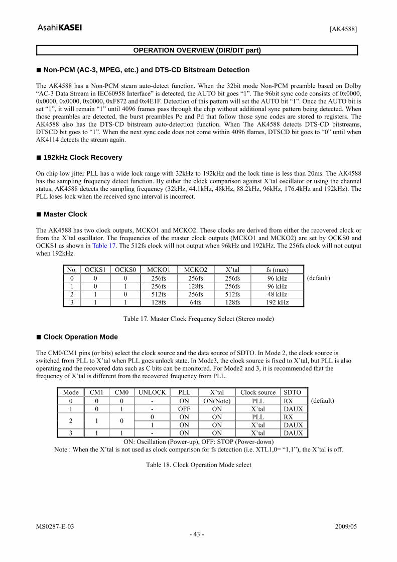
OPERATION OVERVIEW (DIR/DIT part) ■ Non-PCM (AC-3, MPEG, etc.) and DTS-CD Bitstream Detection The AK4588 has a Non-PCM steam auto-detect function. When the 32bit mode Non-PCM preamble based on Dolby “AC-3 Data Stream in IEC60958 Interface” is detected, the AUTO bit goes “1”. The 96bit sync code consists of 0x0000, 0x0000, 0x0000, 0x0000, 0xF872 and 0x4E1F. Detection of this pattern will set the AUTO bit “1”. Once the AUTO bit is set “1”, it will remain “1” until 4096 frames pass through the chip without additional sync pattern being detected. When those preambles are detected, the burst preambles Pc and Pd that follow those sync codes are stored to registers. The AK4588 also has the DTS-CD bitstream auto-detection function. When The AK4588 detects DTS-CD bitstreams, DTSCD bit goes to “1”. When the next sync code does not come within 4096 flames, DTSCD bit goes to “0” until when AK4114 detects the stream again. ■ 192kHz Clock Recovery On chip low jitter PLL has a wide lock range with 32kHz to 192kHz and the lock time is less than 20ms. The AK4588 has the sampling frequency detect function. By either the clock comparison against X’tal oscillator or using the channel status, AK4588 detects the sampling frequency (32kHz, 44.1kHz, 48kHz, 88.2kHz, 96kHz, 176.4kHz and 192kHz). The PLL loses lock when the received sync interval is incorrect. ■ Master Clock The AK4588 has two clock outputs, MCKO1 and MCKO2. These clocks are derived from either the recovered clock or from the X’tal oscillator. The frequencies of the master clock outputs (MCKO1 and MCKO2) are set by OCKS0 and OCKS1 as shown in Table 17. The 512fs clock will not output when 96kHz and 192kHz. The 256fs clock will not output when 192kHz.
No. OCKS1 OCKS0 MCKO1 MCKO2 X’tal fs (max) 0 0 0 256fs 256fs 256fs 96 kHz 1 0 1 256fs 128fs 256fs 96 kHz 2 1 0 512fs 256fs 512fs 48 kHz 3 1 1 128fs 64fs 128fs 192 kHz
(default)
Table 17. Master Clock Frequency Select (Stereo mode)
■ Clock Operation Mode The CM0/CM1 pins (or bits) select the clock source and the data source of SDTO. In Mode 2, the clock source is switched from PLL to X’tal when PLL goes unlock state. In Mode3, the clock source is fixed to X’tal, but PLL is also operating and the recovered data such as C bits can be monitored. For Mode2 and 3, it is recommended that the frequency of X’tal is different from the recovered frequency from PLL.
Mode CM1 CM0 UNLOCK PLL X’tal Clock source SDTO 0 0 0 - ON ON(Note) PLL RX 1 0 1 - OFF ON X’tal DAUX
0 ON ON PLL RX 2 1 0 1 ON ON X’tal DAUX 3 1 1 - ON ON X’tal DAUX
(default)
ON: Oscillation (Power-up), OFF: STOP (Power-down) Note : When the X’tal is not used as clock comparison for fs detection (i.e. XTL1,0= “1,1”), the X’tal is off.
Table 18. Clock Operation Mode select

[AK4588]
MS0287-E-03 2009/05 - 44 -
■ Clock Source The clock for the XTI pin can be generated b following methods. 1) X’tal
XTI
XTO AK4588
25kΩ
C
C
(typ)
Figure 17. X’tal mode
Note: External capacitance depends on the crystal oscillator (Typ. 10-40pF) 2) External clock
XTI
XTOAK4588
25kΩ
ExternalClock
(typ)
XTI
XTOAK4588
25kΩ
ExternalClock
C
(typ)
Figure 18 (5V). (a).External clock mode Figure 19 (3.3V). (b). External clock mode (Input :CMOS Level) (Input : ≥40%DVDD) - Note: Input clock must not exceed DVDD. 3) Fixed to the Clock Operation Mode 0
XTI
XTOAK4588
25kΩ(typ)
Figure 20. OFF mode

[AK4588]
MS0287-E-03 2009/05 - 45 -
■ Sampling Frequency and Pre-emphasis Detection The AK4588 has two methods for detecting the sampling frequency as follows.
1. Clock comparison between recovered clock and X’tal oscillator 2. Sampling frequency information on channel status
Those could be selected by XTL1, 0 bits. And the detected frequency is reported on FS3-0 bits.
XTL1 XTL0 X’tal Frequency 0 0 11.2896MHz 0 1 12.288MHz 1 0 24.576MHz 1 1 (Use channel status)
(default)
Table 19. Reference X’tal frequency
Except XTL1,0= “1,1” XTL1,0= “1,1”
Register output fs Consumer mode
(Note 25)Professional mode
FS3 FS2 FS1 FS0
Clock comparison (Note 24)
Byte3 Bit3/2/1/0
Byte0 Bit7/6
Byte4 Bit6/5/4/3
0 0 0 0 44.1kHz 44.1kHz 0 0 0 0 0 1 0 0 0 0 0 0 0 1 Reserved Reserved 0 0 0 1 (Others) 0 0 1 0 48kHz 48kHz 0 0 1 0 1 0 0 0 0 0 0 0 1 1 32kHz 32kHz 0 0 1 1 1 1 0 0 0 0 1 0 0 0 88.2kHz 88.2kHz ( 1 0 0 0 ) 0 0 1 0 1 0 1 0 1 0 96kHz 96kHz ( 1 0 1 0 ) 0 0 0 0 1 0 1 1 0 0 176.4kHz 176.4kHz ( 1 1 0 0 ) 0 0 1 0 1 1 1 1 1 0 192kHz 192kHz ( 1 1 1 0 ) 0 0 0 0 1 1
Note 24. At least ±3% range is identified as the value in the Table 20. In case of intermediate frequency of those two, FS3-0 bits indicate nearer value. When the frequency is much bigger than 192kHz or much smaller than 32kHz, FS3-0 bits may indicate “0001”.
Note 25. When consumer mode, Byte3 Bit3-0 are copied to FS3-0 bits.
Table 20. fs Information The pre-emphasis information is detected and reported on PEM bit. These information are extracted from channel 1 at default. It can be switched to channel 2 by CS12 bit in control register.
PEM Pre-emphasis Byte 0 Bits 3-5
0 OFF ≠ 0X1001 ON 0X100
Table 21. PEM in Consumer Mode
PEM Pre-emphasis Byte 0 Bits 2-4
0 OFF ≠110 1 ON 110
Table 22. PEM in Professional Mode

[AK4588]
MS0287-E-03 2009/05 - 46 -
■ De-emphasis Filter Control The AK4588 has a digital de-emphasis filter (tc=50/15µs) which corresponds to four sampling frequencies (32kHz, 44.1kHz, 48kHz and 96kHz) by IIR filter. When DEAU bit=“1”, the de-emphasis filter is enabled automatically by sampling frequency and pre-emphasis information in the channel status. This is the default setting of de-emphasis filter of the AK4588. In Serial Mode, DEM0/1 and DFS bits can control the de-emphasis filter when DEAU bit is “0”. The internal de-emphasis filter is bypassed and the recovered data is output without any change if either pre-emphasis or de-emphasis Mode is OFF.
PEM FS3 FS2 FS1 FS0 Mode 1 0 0 0 0 44.1kHz 1 0 0 1 0 48kHz 1 0 0 1 1 32kHz 1 1 0 1 0 96kHz 1 (Others) OFF 0 x x x x OFF
(x: Don’t care) Table 23. De-emphasis Auto Control at DEAU bit = “1” (Default)
PEM DFS DEM1 DEM0 Mode
1 0 0 0 44.1kHz 1 0 0 1 OFF (default)1 0 1 0 48kHz 1 0 1 1 32kHz 1 1 0 0 OFF 1 1 0 1 OFF 1 1 1 0 96kHz 1 1 1 1 OFF 0 x x x OFF
(x: Don’t care) Table 24. De-emphasis Manual Control at DEAU bit = “0”
■ System Reset and Power-Down The AK4588 has power-down mode for all circuits by the PDN pin and partially powered-down by PWN bit. The RSTN bit initializes the register and resets the internal timing. In Parallel Mode, only the control by PDN pin is enabled. The AK4588 should be reset once by bringing the PDN pin = “L” upon power-up. PDN Pin: All analog and digital circuit are placed in the power-down and reset mode by bringing the PDN pin = “L”. All
registers are initialized, and clocks are stopped. Reading and witting to the register are disabled. RSTN2 Bit (Address 00H; D0):
All the registers except PWN and RSTN2 bits are initialized by bringing RSTN2 bit = “0”. The internal timings are also initialized. Witting to the register is not available except PWN and RSTN2 bits. Reading to the register is disabled.
PWN Bit (Address 00H; D1):
The clock recovery part is initialized by bringing PWN bit = “0”. In this case, clocks are stopped. The registers are not initialized and the mode settings are kept. Writing and Reading to the registers are enabled.

[AK4588]
MS0287-E-03 2009/05 - 47 -
■ Biphase Input and Through Output Eight receiver inputs (RX0-7) are available in Serial Control Mode. Each input includes amplifier corresponding to unbalance mode and can accept the signal of 200mV or more. IPS2-0 bits selects the receiver channel. When BCU bit = “1”, the Block start signal, C bit and U bit can be output from each pins.
IPS2 IPS1 IPS0 INPUT Data 0 0 0 RX0 (default) 0 0 1 RX1 0 1 0 RX2 0 1 1 RX3 1 0 0 RX4 1 0 1 RX5 1 1 0 RX6 1 1 1 RX7
Table 25. Recovery Data Select
B
COUT (or U,V)
LRCK2 (except I2S)
C(L0) C(R0) C(L1) C(R31) C(L31) C(L32) C(R191)
1/4fs
SDTO2
L191 R191 L30 L31 R30 L0R190
LRCK2 (I2S)
Figure 21. B/C/U/V output/input timings

[AK4588]
MS0287-E-03 2009/05 - 48 -
■ Biphase Output The AK4588 can output the data either the through output(from DIR) or transmitter output(DIT; the data from DAUX2 is transformed to IEC60958 format.) from TX1/0 pins. Those could be selected by DIT bit. The source of the through output from TX0 could be selected among RX0-8 by OPS00/ 01/ 02 bits, for TX1, by OPS10/ 11/ 12 bits respectively. When output DAUX2 data, V bit could be controlled by the VIN pin and first 5 bytes of C bit could be controlled by CT39-CT0 bits in control registers. When bit0= “0”(consumer mode), bit20-23 (Audio channel) could not be controlled directly but be controlled by CT20 bit. When the CT20 bit is “1”, the AK4588 outputs “1000” as C20-23 for left channel and output “0100” at C20-23 for right channel automatically. When CT20 bit is “0”, the AK4588 outputs “0000” set as “1000” for sub frame 1, and “0100” for sub frame 2. U bits are fixed to “0”.as C20-23 for both channel. U bit could be controlled by UDIT bit as follows; When UDIT bit is “0”, U bit is always “0”. When UDIT bit is “1”, the recovered U bits are used for DIT (DIR/DIT loop mode of U bit). This mode is only available when PLL is locked in master mode.
OPS02 OPS01 OPS00 Output Data 0 0 0 RX0 (default) 0 0 1 RX1 0 1 0 RX2 0 1 1 RX3 1 0 0 RX4 1 0 1 RX5 1 1 0 RX6 1 1 1 RX7
Table 26. Output Data Select for TX0
DIT OPS12 OPS11 OPS10 Output Data
0 0 0 0 RX0 0 0 0 1 RX1 0 0 1 0 RX2 0 0 1 1 RX3 0 1 0 0 RX4 0 1 0 1 RX5 0 1 1 0 RX6 0 1 1 1 RX7 1 x x x DAUX2 (default)
Table 27. Output Data Select for TX1
LRCK2 (I2S)
VIN
L0 R0 L1 DAUX2
L0 R0 L1R191
R1
LRCK2 (except I2S)
Figure 22. DAUX2 and VIN input timings

[AK4588]
MS0287-E-03 2009/05 - 49 -
■ Biphase signal input/output circuit
RX
AK4588
0.1uF
75Ω Coax
75Ω
Figure 23. Consumer Input Circuit (Coaxial Input)
Note: In case of coaxial input, if a coupling level to this input from the next RX input line pattern exceeds 50mV, there is a possibility of malfunction. Connecting a decoupling capacitor can lower this coupling noise.
RX
AK4588
470
O/E
Optical ReceiverOptical Fiber
Figure 24. Consumer Input Circuit (Optical Input) For coaxial input, as the input level of RX line is small in Serial Mode, cross-talking among RX input lines have to be avoided. For example, by inserting the shield pattern among them. In Parallel Mode, only one channel input (RX1) is available and RX2-4 change to other pins for audio format control. Those pins must be fixed to “H” or “L”.
The AK4588 has a TX output buffer. The output level meets 0.5V+/-20% with the external resistors. The T1 in Figure 25 is a transformer of 1:1.
TX
DVSS
100±2%
T1
75Ω cable
330±2%
Figure 25. TX External Resistor Network
[AK4588]
MS0287-E-03 2009/05 - 50 -
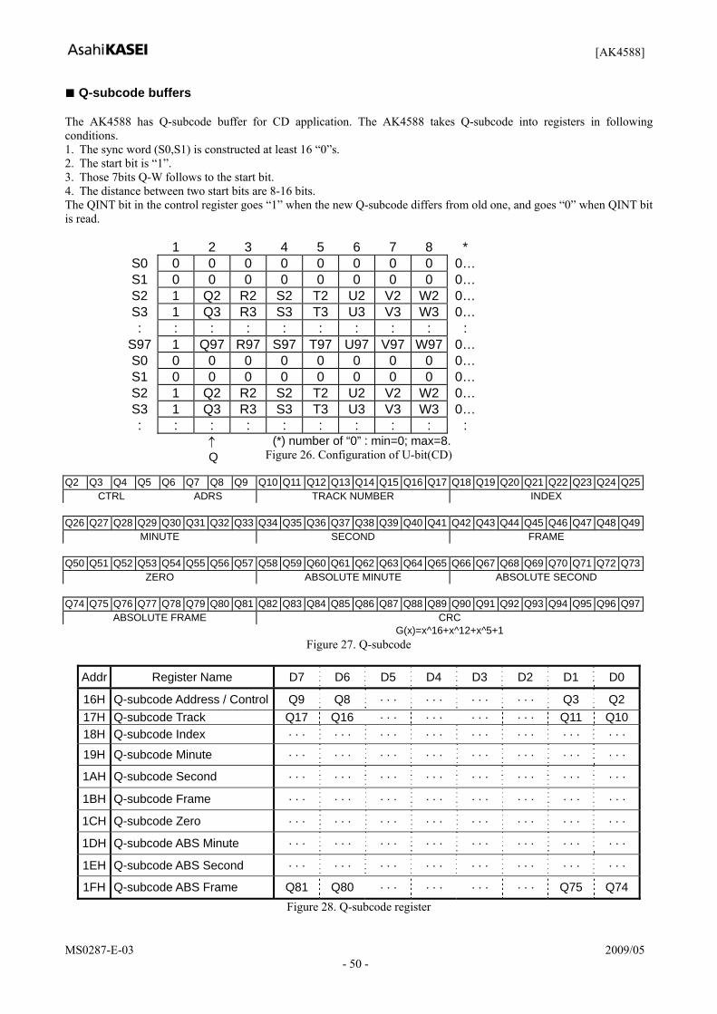
■ Q-subcode buffers The AK4588 has Q-subcode buffer for CD application. The AK4588 takes Q-subcode into registers in following conditions. 1. The sync word (S0,S1) is constructed at least 16 “0”s. 2. The start bit is “1”. 3. Those 7bits Q-W follows to the start bit. 4. The distance between two start bits are 8-16 bits. The QINT bit in the control register goes “1” when the new Q-subcode differs from old one, and goes “0” when QINT bit is read.
1 2 3 4 5 6 7 8 * S0 0 0 0 0 0 0 0 0 0…S1 0 0 0 0 0 0 0 0 0…S2 1 Q2 R2 S2 T2 U2 V2 W2 0…S3 1 Q3 R3 S3 T3 U3 V3 W3 0…: : : : : : : : : :
S97 1 Q97 R97 S97 T97 U97 V97 W97 0…S0 0 0 0 0 0 0 0 0 0…S1 0 0 0 0 0 0 0 0 0…S2 1 Q2 R2 S2 T2 U2 V2 W2 0…S3 1 Q3 R3 S3 T3 U3 V3 W3 0…: : : : : : : : : :
(*) number of “0” : min=0; max=8. Figure 26. Configuration of U-bit(CD)
Q2 Q3 Q4 Q5 Q6 Q7 Q8 Q9 Q10 Q11 Q12 Q13 Q14 Q15 Q16 Q17 Q18 Q19 Q20 Q21 Q22 Q23 Q24 Q25
CTRL ADRS TRACK NUMBER INDEX
Q26 Q27 Q28 Q29 Q30 Q31 Q32 Q33 Q34 Q35 Q36 Q37 Q38 Q39 Q40 Q41 Q42 Q43 Q44 Q45 Q46 Q47 Q48 Q49MINUTE SECOND FRAME
Q50 Q51 Q52 Q53 Q54 Q55 Q56 Q57 Q58 Q59 Q60 Q61 Q62 Q63 Q64 Q65 Q66 Q67 Q68 Q69 Q70 Q71 Q72 Q73
ZERO ABSOLUTE MINUTE ABSOLUTE SECOND
Q74 Q75 Q76 Q77 Q78 Q79 Q80 Q81 Q82 Q83 Q84 Q85 Q86 Q87 Q88 Q89 Q90 Q91 Q92 Q93 Q94 Q95 Q96 Q97ABSOLUTE FRAME CRC
G(x)=x^16+x^12+x^5+1 Figure 27. Q-subcode
Addr Register Name D7 D6 D5 D4 D3 D2 D1 D0
16H Q-subcode Address / Control Q9 Q8 · · · · · · · · · · · · Q3 Q2 17H Q-subcode Track Q17 Q16 · · · · · · · · · · · · Q11 Q1018H Q-subcode Index · · · · · · · · · · · · · · · · · · · · · · · ·
19H Q-subcode Minute · · · · · · · · · · · · · · · · · · · · · · · ·
1AH Q-subcode Second · · · · · · · · · · · · · · · · · · · · · · · ·
1BH Q-subcode Frame · · · · · · · · · · · · · · · · · · · · · · · ·
1CH Q-subcode Zero · · · · · · · · · · · · · · · · · · · · · · · ·
1DH Q-subcode ABS Minute · · · · · · · · · · · · · · · · · · · · · · · ·
1EH Q-subcode ABS Second · · · · · · · · · · · · · · · · · · · · · · · ·
1FH Q-subcode ABS Frame Q81 Q80 · · · · · · · · · · · · Q75 Q74Figure 28. Q-subcode register
↑ Q
[AK4588]
MS0287-E-03 2009/05 - 51 -
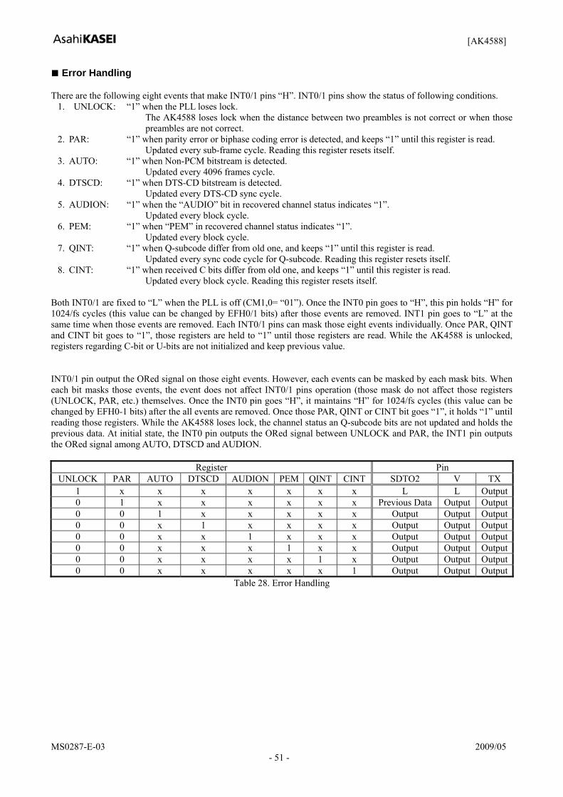
■ Error Handling There are the following eight events that make INT0/1 pins “H”. INT0/1 pins show the status of following conditions.
1. UNLOCK: “1” when the PLL loses lock. The AK4588 loses lock when the distance between two preambles is not correct or when those preambles are not correct.
2. PAR: “1” when parity error or biphase coding error is detected, and keeps “1” until this register is read. Updated every sub-frame cycle. Reading this register resets itself.
3. AUTO: “1” when Non-PCM bitstream is detected. Updated every 4096 frames cycle.
4. DTSCD: “1” when DTS-CD bitstream is detected. Updated every DTS-CD sync cycle.
5. AUDION: “1” when the “AUDIO” bit in recovered channel status indicates “1”. Updated every block cycle.
6. PEM: “1” when “PEM” in recovered channel status indicates “1”. Updated every block cycle.
7. QINT: “1” when Q-subcode differ from old one, and keeps “1” until this register is read. Updated every sync code cycle for Q-subcode. Reading this register resets itself.
8. CINT: “1” when received C bits differ from old one, and keeps “1” until this register is read. Updated every block cycle. Reading this register resets itself.
Both INT0/1 are fixed to “L” when the PLL is off (CM1,0= “01”). Once the INT0 pin goes to “H”, this pin holds “H” for 1024/fs cycles (this value can be changed by EFH0/1 bits) after those events are removed. INT1 pin goes to “L” at the same time when those events are removed. Each INT0/1 pins can mask those eight events individually. Once PAR, QINT and CINT bit goes to “1”, those registers are held to “1” until those registers are read. While the AK4588 is unlocked, registers regarding C-bit or U-bits are not initialized and keep previous value. INT0/1 pin output the ORed signal on those eight events. However, each events can be masked by each mask bits. When each bit masks those events, the event does not affect INT0/1 pins operation (those mask do not affect those registers (UNLOCK, PAR, etc.) themselves. Once the INT0 pin goes “H”, it maintains “H” for 1024/fs cycles (this value can be changed by EFH0-1 bits) after the all events are removed. Once those PAR, QINT or CINT bit goes “1”, it holds “1” until reading those registers. While the AK4588 loses lock, the channel status an Q-subcode bits are not updated and holds the previous data. At initial state, the INT0 pin outputs the ORed signal between UNLOCK and PAR, the INT1 pin outputs the ORed signal among AUTO, DTSCD and AUDION.
Register Pin UNLOCK PAR AUTO DTSCD AUDION PEM QINT CINT SDTO2 V TX
1 x x x x x x x L L Output0 1 x x x x x x Previous Data Output Output0 0 1 x x x x x Output Output Output0 0 x 1 x x x x Output Output Output0 0 x x 1 x x x Output Output Output0 0 x x x 1 x x Output Output Output0 0 x x x x 1 x Output Output Output0 0 x x x x x 1 Output Output Output
Table 28. Error Handling

[AK4588]
MS0287-E-03 2009/05 - 52 -
Error (UNLOCK, PAR,..)
INT1 pin
SDTO2 (UNLOCK)
MCKO,BICK2,LRCK2 (UNLOCK)
Previous Data
Register (PAR,CINT,QINT) Hold ”1”
Command READ 06H
MCKO,BICK2,LRCK2 (except UNLOCK)
(fs: around 20kHz)
SDTO2 (PAR error)
Hold Time = 0
Reset
(Error)
SDTO2 (others)
Normal Operation
INT0 pin Hold Time (max: 4096/fs)
Register (others)
Free Run
VOUT pin (UNLOCK)
VOUT pin (except UNLOCK)
Figure 29. INT0/1 pin timing

[AK4588]
MS0287-E-03 2009/05 - 53 -
INT0/1 pin ="H"
No
Yes
Yes
Initialize
PDN pin ="L" to "H"
Read 06H
Mute DAC output
Read 06H
No
(Each Error Handling)
Read 06H(Resets registers)
INT0/1 pin ="H"
Release Muting
Figure 30. Error Handling Sequence Example 1

[AK4588]
MS0287-E-03 2009/05 - 54 -
INT1 pin ="H"
No
Yes
Initialize
PDN pin ="L" to "H"
Read 06H
Read 06H and
Detect QSUB= “1”
No
(Read Q-buffer)
New data is valid
INT1 pin ="L"
QCRC = “0”
Yes
Yes
New data is invalid
No
Figure 31. Error Handling Sequence Example 2 (for Q/CINT)
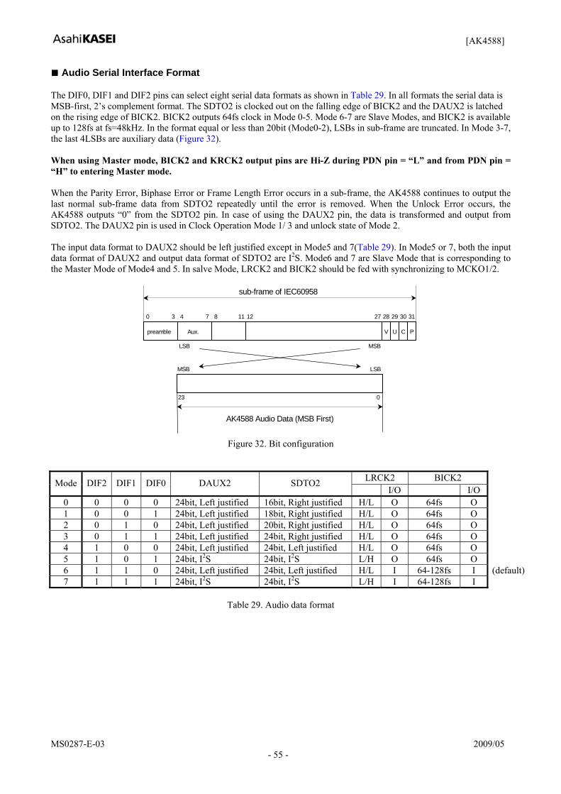
[AK4588]
MS0287-E-03 2009/05 - 55 -
■ Audio Serial Interface Format The DIF0, DIF1 and DIF2 pins can select eight serial data formats as shown in Table 29. In all formats the serial data is MSB-first, 2’s complement format. The SDTO2 is clocked out on the falling edge of BICK2 and the DAUX2 is latched on the rising edge of BICK2. BICK2 outputs 64fs clock in Mode 0-5. Mode 6-7 are Slave Modes, and BICK2 is available up to 128fs at fs=48kHz. In the format equal or less than 20bit (Mode0-2), LSBs in sub-frame are truncated. In Mode 3-7, the last 4LSBs are auxiliary data (Figure 32). When using Master mode, BICK2 and KRCK2 output pins are Hi-Z during PDN pin = “L” and from PDN pin = “H” to entering Master mode. When the Parity Error, Biphase Error or Frame Length Error occurs in a sub-frame, the AK4588 continues to output the last normal sub-frame data from SDTO2 repeatedly until the error is removed. When the Unlock Error occurs, the AK4588 outputs “0” from the SDTO2 pin. In case of using the DAUX2 pin, the data is transformed and output from SDTO2. The DAUX2 pin is used in Clock Operation Mode 1/ 3 and unlock state of Mode 2. The input data format to DAUX2 should be left justified except in Mode5 and 7(Table 29). In Mode5 or 7, both the input data format of DAUX2 and output data format of SDTO2 are I2S. Mode6 and 7 are Slave Mode that is corresponding to the Master Mode of Mode4 and 5. In salve Mode, LRCK2 and BICK2 should be fed with synchronizing to MCKO1/2.
0 3 4 7 8 11 12 27 28 29 30 31
preamble Aux.
LSB MSB
V U C P
sub-frame of IEC60958
023
AK4588 Audio Data (MSB First)
LSBMSB
Figure 32. Bit configuration
LRCK2 BICK2 Mode DIF2 DIF1 DIF0 DAUX2 SDTO2 I/O I/O
0 0 0 0 24bit, Left justified 16bit, Right justified H/L O 64fs O 1 0 0 1 24bit, Left justified 18bit, Right justified H/L O 64fs O 2 0 1 0 24bit, Left justified 20bit, Right justified H/L O 64fs O 3 0 1 1 24bit, Left justified 24bit, Right justified H/L O 64fs O 4 1 0 0 24bit, Left justified 24bit, Left justified H/L O 64fs O 5 1 0 1 24bit, I2S 24bit, I2S L/H O 64fs O 6 1 1 0 24bit, Left justified 24bit, Left justified H/L I 64-128fs I (default) 7 1 1 1 24bit, I2S 24bit, I2S L/H I 64-128fs I
Table 29. Audio data format

[AK4588]
MS0287-E-03 2009/05 - 56 -
LRCK2
BICK2(0:64fs)
SDTO2
0 1 2 31 0 1
15:MSB, 0:LSB
Lch Data Rch Data
15 17 16 1531 0 1 2 1716
0 1 0 1
15 14 14 15
Figure 33. Mode 0 Timing
LRCK2
BICK2(0:64fs)
SDTO2
0 1 2 31 0 1
23:MSB, 0:LSB
Lch Data Rch Data
9 11 10 931 0 1 2 1110
0 1 0 1
12
21 20 20 21
12
22 23 2223
Figure 34. Mode 3 Timing
LRCK2
BICK2(64fs)
SDTO2
0 1 2 31 0 1
23:MSB, 0:LSB
Lch Data Rch Data
21 23 22 2131 0 1 2 2322
23 222
24
1 0 0 1
24
21 22 23 3 2 23 22
Figure 35. Mode 4/6 Timing Mode4: LRCK2, BICK2: Output
Mode6: LRCK2, BICK2: Input
LRCK2
BICK2(64fs)
SDTO2
0 1 2 31 0 1
23:MSB, 0:LSB
Lch Data Rch Data
23 22 2131 0 1 2 2322
23 22
24
1 0
24
3 2 23
25
2 01 21 22 23
25
Figure 36. Mode 5/7 Timing Mode5: LRCK2, BICK2: Output
Mode7: LRCK2, BICK2: Input

[AK4588]
MS0287-E-03 2009/05 - 57 -
■ Register Map Addr Register Name D7 D6 D5 D4 D3 D2 D1 D0
00H CLK & Power Down Control CS12 BCU CM1 CM0 OCKS1 OCKS0 PWN RSTN2
01H Format & De-em Control 0 DIF2 DIF1 DIF0 DEAU DEM1 DEM0 DFS 02H Input/ Output Control 0 TX1E OPS12 OPS11 OPS10 TX0E OPS02 OPS01 OPS00 03H Input/ Output Control 1 EFH1 EFH0 UDIT 0 DIT IPS2 IPS1 IPS0 04H INT0 MASK MQIT0 MAUT0 MCIT0 MULK0 MDTS0 MPE0 MAUD0 MPAR005H INT1 MASK MQIT1 MAUT1 MCIT1 MULK1 MDTS1 MPE1 MAUD1 MPAR106H Receiver status 0 QINT AUTO CINT UNLCK DTSCD PEM AUDION PAR 07H Receiver status 1 FS3 FS2 FS1 FS0 0 V QCRC CCRC 08H RX Channel Status Byte 0 CR7 CR6 CR5 CR4 CR3 CR2 CR1 CR0 09H RX Channel Status Byte 1 CR15 CR14 CR13 CR12 CR11 CR10 CR9 CR8 0AH RX Channel Status Byte 2 CR23 CR22 CR21 CR20 CR19 CR18 CR17 CR16 0BH RX Channel Status Byte 3 CR31 CR30 CR29 CR28 CR27 CR26 CR25 CR24 0CH RX Channel Status Byte 4 CR39 CR38 CR37 CR36 CR35 CR34 CR33 CR32 0DH TX Channel Status Byte 0 CT7 CT6 CT5 CT4 CT3 CT2 CT1 CT0
0EH TX Channel Status Byte 1 CT15 CT14 CT13 CT12 CT11 CT10 CT9 CT8
0FH TX Channel Status Byte 2 CT23 CT22 CT21 CT20 CT19 CT18 CT17 CT16
10H TX Channel Status Byte 3 CT31 CT30 CT29 CT28 CT27 CT26 CT25 CT24
11H TX Channel Status Byte 4 CT39 CT39 CT39 CT39 CT39 CT39 CT39 CT32
12H Burst Preamble Pc Byte 0 PC7 PC6 PC5 PC4 PC3 PC2 PC1 PC0 13H Burst Preamble Pc Byte 1 PC15 PC14 PC13 PC12 PC11 PC10 PC9 PC8 14H Burst Preamble Pd Byte 0 PD7 PD6 PD5 PD4 PD3 PD2 PD1 PD0 15H Burst Preamble Pd Byte 1 PD15 PD14 PD13 PD12 PD11 PD10 PD9 PD8 16H Q-subcode Address / Control Q9 Q8 Q7 Q6 Q5 Q4 Q3 Q2 17H Q-subcode Track Q17 Q16 Q15 Q14 Q13 Q12 Q11 Q10 18H Q-subcode Index Q25 Q24 Q23 Q22 Q21 Q20 Q19 Q18 19H Q-subcode Minute Q33 Q32 Q31 Q30 Q29 Q28 Q27 Q26 1AH Q-subcode Second Q41 Q40 Q39 Q38 Q37 Q36 Q35 Q34 1BH Q-subcode Frame Q49 Q48 Q47 Q46 Q45 Q44 Q43 Q42 1CH Q-subcode Zero Q57 Q56 Q55 Q54 Q53 Q52 Q51 Q50 1DH Q-subcode ABS Minute Q65 Q64 Q63 Q62 Q61 Q60 Q59 Q58 1EH Q-subcode ABS Second Q73 Q72 Q71 Q70 Q69 Q68 Q67 Q66 1FH Q-subcode ABS Frame Q81 Q80 Q79 Q78 Q77 Q76 Q75 Q74
When PDN pin goes “L”, the registers are initialized to their default values. When RSTN bit goes “0”, the internal timing is reset and the registers are initialized to their default values. All data can be written to the register even if PWN bit is “0”. 01H D7 and 03H D4 should be written “0” data.

[AK4588]
MS0287-E-03 2009/05 - 58 -
■ Register Definitions Reset & Initialize Addr Register Name D7 D6 D5 D4 D3 D2 D1 D0 00H CLK & Power Down Control CS12 BCU CM1 CM0 OCKS1 OCKS0 PWN RSTN2
R/W R/W R/W R/W R/W R/W R/W R/W R/W Default 0 1 0 0 0 0 1 1
RSTN2: Timing Reset & Register Initialize
0: Reset & Initialize 1: Normal Operation
PWN: Power Down 0: Power Down 1: Normal Operation
OCKS1-0: Master Clock Frequency Select CM1-0: Master Clock Operation Mode Select BCU: Block start & C/U Output Mode
When BCU=1, the three Output Pins(BOUT, COUT, UOUT) become to be enabled. The block signal goes high at the start of frame 0 and remains high until the end of frame 31.
CS12: Channel Status Select 0: Channel 1 1: Channel 2 Selects which channel status is used to derive C-bit buffers, AUDION, PEM, FS3, FS2, FS1, FS0, Pc and Pd. The de-emphasis filter is controlled by channel 1 in the Parallel Mode.
Format & De-emphasis Control
Addr Register Name D7 D6 D5 D4 D3 D2 D1 D0 01H Format & De-em Control 0 DIF2 DIF1 DIF0 DEAU DEM1 DEM0 DFS
R/W RD R/W R/W R/W R/W R/W R/W R/WDefault 0 1 1 0 1 0 1 0
DFS: 96kHz De-emphasis Control DEM1-0: 32, 44.1, 48kHz De-emphasis Control (Table 24.) DEAU: De-emphasis Auto Detect Enable
0: Disable 1: Enable
DIF2-0: Audio Data Format Control (Table 29.)

[AK4588]
MS0287-E-03 2009/05 - 59 -
Input/Output Control
Addr Register Name D7 D6 D5 D4 D3 D2 D1 D0 02H Input/ Output Control 0 TX1E OPS12 OPS11 OPS10 TX0E OPS02 OPS01 OPS00
R/W R/W R/W R/W R/W R/W R/W R/W R/WDefault 1 0 0 0 1 0 0 0
OPS02-00: Output Through Data Select for TX0 pin OPS12-10: Output Through Data Select for TX1 pin TX0E: TX0 Output Enable
0: Disable. TX0 pin outputs “L”. 1: Enable
TX1E: TX1 Output Enable 0: Disable. TX1 pin outputs “L”. 1: Enable
Addr Register Name D7 D6 D5 D4 D3 D2 D1 D0 03H Input/ Output Control 1 EFH1 EFH0 UDIT 0 DIT IPS2 IPS1 IPS0
R/W R/W R/W R/W RD R/W R/W R/W R/WDefault 0 1 0 0 1 0 0 0
IPS2-0: Input Recovery Data Select DIT: Through data/Transmit data select for TX1 pin
0: Through data (RX data). 1: Transmit data (DAUX2 data).
UDIT: U bit control for DIT 0: U bit is fixed to “0” 1: Recovered U bit is used for DIT (loop mode for U bit)
EFH1-0: Interrupt 0 Pin Hold Count Select 00: 512 LRCK2 01: 1024 LRCK2 10: 2048 LRCK2 11: 4096 LRCK2

[AK4588]
MS0287-E-03 2009/05 - 60 -
Mask Control for INT0
Addr Register Name D7 D6 D5 D4 D3 D2 D1 D0 04H INT0 MASK MQI0 MAT0 MCI0 MUL0 MDTS0 MPE0 MAN0 MPR0
R/W R/W R/W R/W R/W R/W R/W R/W R/W Default 1 1 1 0 1 1 1 0
MPR0: Mask Enable for PAR bit MAN0: Mask Enable for AUDN bit MPE0: Mask Enable for PEM bit MDTS0: Mask Enable for DTSCD bit MUL0: Mask Enable for UNLOCK bit MCI0: Mask Enable for CINT bit MAT0: Mask Enable for AUTO bit MQI0: Mask Enable for QINT bit
0: Mask disable 1: Mask enable
Mask Control for INT1
Addr Register Name D7 D6 D5 D4 D3 D2 D1 D0 05H INT1 MASK MQI1 MAT1 MCI1 MUL1 MDTS1 MPE1 MAN1 MPR1
R/W R/W R/W R/W R/W R/W R/W R/W R/W Default 1 0 1 1 0 1 0 1
MPR1: Mask Enable for PAR bit MAN1: Mask Enable for AUDN bit MPE1: Mask Enable for PEM bit MDTS1: Mask Enable for DTSCD bit MUL1: Mask Enable for UNLOCK0 bit MCI1: Mask Enable for CINT bit MAT1: Mask Enable for AUTO bit MQI1: Mask Enable for QINT bit
0: Mask disable 1: Mask enable

[AK4588]
MS0287-E-03 2009/05 - 61 -
Receiver Status 0
Addr Register Name D7 D6 D5 D4 D3 D2 D1 D0 06H Receiver status 0 QINT AUTO CINT UNLCK DTSCD PEM AUDION PAR
R/W RD RD RD RD RD RD RD RD Default 0 0 0 0 0 0 0 0
PAR: Parity Error or Biphase Error Status
0:No Error 1:Error It is “1” if Parity Error or Biphase Error is detected in the sub-frame.
AUDION: Audio Bit Output 0: Audio 1: Non Audio This bit is made by encoding channel status bits.
PEM: Pre-emphasis Detect. 0: OFF 1: ON This bit is made by encoding channel status bits.
DTSCD: DTS-CD Auto Detect 0: No detect 1: Detect
UNLCK: PLL Lock Status 0: Locked 1: Out of Lock
CINT: Channel Status Buffer Interrupt 0: No change 1: Changed
AUTO: Non-PCM Auto Detect 0: No detect 1: Detect
QINT: Q-subcode Buffer Interrupt 0: No change 1: Changed
QINT, CINT and PAR bits are initialized when 06H is read.
Receiver Status 1
Addr Register Name D7 D6 D5 D4 D3 D2 D1 D0 07H Receiver status 1 FS3 FS2 FS1 FS0 0 V QCRC CCRC
R/W RD RD RD RD RD RD RD RD Default 0 0 0 1 0 0 0 0
CCRC: Cyclic Redundancy Check for Channel Status
0:No Error 1:Error QCRC: Cyclic Redundancy Check for Q-subcode
0:No Error 1:Error V: Validity of channel status
0:Valid 1:Invalid FS3-0: Sampling Frequency detection (Table 20.)

[AK4588]
MS0287-E-03 2009/05 - 62 -
Receiver Channel Status
Addr Register Name D7 D6 D5 D4 D3 D2 D1 D0 08H RX Channel Status Byte 0 CR7 CR6 CR5 CR4 CR3 CR2 CR1 CR0 09H RX Channel Status Byte 1 CR15 CR14 CR13 CR12 CR11 CR10 CR9 CR8 0AH RX Channel Status Byte 2 CR23 CR22 CR21 CR20 CR19 CR18 CR17 CR160BH RX Channel Status Byte 3 CR31 CR30 CR29 CR28 CR27 CR26 CR25 CR240CH RX Channel Status Byte 4 CR39 CR38 CR37 CR36 CR35 CR34 CR33 CR32
R/W RD Default Not initialized
CR39-0: Receiver Channel Status Byte 4-0
Transmitter Channel Status
Addr Register Name D7 D6 D5 D4 D3 D2 D1 D0 0DH TX Channel Status Byte 0 CT7 CT6 CT5 CT4 CT3 CT2 CT1 CT0 0EH TX Channel Status Byte 1 CT15 CT14 CT13 CT12 CT11 CT10 CT9 CT8 0FH TX Channel Status Byte 2 CT23 CT22 CT21 CT20 CT19 CT18 CT17 CT1610H TX Channel Status Byte 3 CT31 CT30 CT29 CT28 CT27 CT26 CT25 CT2411H TX Channel Status Byte 3 CT39 CT38 CT37 CT36 CT35 CT34 CT335 CT32
R/W R/W Default 0
CT39-0: Transmitter Channel Status Byte 4-0
Burst Preamble Pc/Pd in non-PCM encoded Audio Bitstreams
Addr Register Name D7 D6 D5 D4 D3 D2 D1 D0 12H Burst Preamble Pc Byte 0 PC7 PC6 PC5 PC4 PC3 PC2 PC1 PC0 13H Burst Preamble Pc Byte 1 PC15 PC14 PC13 PC12 PC11 PC10 PC9 PC8 14H Burst Preamble Pd Byte 0 PD7 PD6 PD5 PD4 PD3 PD2 PD1 PD0 15H Burst Preamble Pd Byte 1 PD15 PD14 PD13 PD12 PD11 PD10 PD9 PD8
R/W RD Default Not initialized
PC15-0: Burst Preamble Pc Byte 0 and 1 PD15-0: Burst Preamble Pd Byte 0 and 1

[AK4588]
MS0287-E-03 2009/05 - 63 -
Q-subcode Buffer
Addr Register Name D7 D6 D5 D4 D3 D2 D1 D0 16H Q-subcode Address / Control Q9 Q8 Q7 Q6 Q5 Q4 Q3 Q2 17H Q-subcode Track Q17 Q16 Q15 Q14 Q13 Q12 Q11 Q10 18H Q-subcode Index Q25 Q24 Q23 Q22 Q21 Q20 Q19 Q18 19H Q-subcode Minute Q33 Q32 Q31 Q30 Q29 Q28 Q27 Q26 1AH Q-subcode Second Q41 Q40 Q39 Q38 Q37 Q36 Q35 Q34 1BH Q-subcode Frame Q49 Q48 Q47 Q46 Q45 Q44 Q43 Q42 1CH Q-subcode Zero Q57 Q56 Q55 Q54 Q53 Q52 Q51 Q50 1DH Q-subcode ABS Minute Q65 Q64 Q63 Q62 Q61 Q60 Q59 Q58 1EH Q-subcode ABS Second Q73 Q72 Q71 Q70 Q69 Q68 Q67 Q66 1FH Q-subcode ABS Frame Q81 Q80 Q79 Q78 Q77 Q76 Q75 Q74
R/W RD Default Not initialized

[AK4588]
MS0287-E-03 2009/05 - 64 -
■ Burst Preambles in non-PCM Bitstreams
0
16 bits of bitstream
3 4 7 8 11 12 27 28 29 30 31
preamble Aux. LSB MSB V U C P
sub-frame of IEC958
0 15
Pa Pb Pc Pd Burst_payload stuffing
repetition time of the burst
Figure 37. Data structure in IEC60958
Preamble word Length of field Contents Value Pa 16 bits sync word 1 0xF872 Pb 16 bits sync word 2 0x4E1F Pc 16 bits Burst info see Table 31 Pd 16 bits Length code Numbers of bits
Table 30. Burst preamble words

[AK4588]
MS0287-E-03 2009/05 - 65 -
Bits of Pc Value Contents Repetition time of burst in IEC60958 frames
0-4 0 1 2 3 4 5 6 7 8 9 10 11 12 13 14 15 16-31
data type NULL data Dolby AC-3 data reserved PAUSE MPEG-1 Layer1 data MPEG-1 Layer2 or 3 data or MPEG-2 without extensionMPEG-2 data with extension MPEG-2 AAC ADTS MPEG-2, Layer1 Low sample rate MPEG-2, Layer2 or 3 Low sample rate reserved DTS type I DTS type II DTS type III ATRAC ATRAC2/3 reserved
≤4096 1536 384 1152 1152 1024 384 1152 512 1024 2048 512 1024
5, 6 0 reserved, shall be set to “0” 7 0
1 error-flag indicating a valid burst_payload error-flag indicating that the burst_payload may contain errors
8-12 data type dependent info 13-15 0 bit stream number, shall be set to “0”
Table 31. Fields of burst info Pc

[AK4588]
MS0287-E-03 2009/05 - 66 -
■ Non-PCM Bitstream timing 1) When Non-PCM preamble is not coming within 4096 frames,
Pa Pc1 Pd1Pb Pa Pc2 Pd2Pb Pa Pc3 Pd3Pb
“0” Pc1 Pc2
“0” Pd1 Pd2 Pd3
Pc3
PDN pin
Bit stream
AUTO bit
Pc Register
Pd Register
Repetition time >4096 frames
Figure 38. Timing example 1
2) When Non-PCM bitstream stops (when MULK0= “0”),
Pa Pc1 Pd1Pb Stop Pa Pcn PdnPb
Pc0 Pc1
Pd0 Pd1 Pdn
Pcn
INT0 pin
Bit stream
AUTO bit
Pc Register
Pd Register
INT0 hold time
2~3 Syncs (B,M or W)
<20mS (Lock time)
<Repetition time
Figure 39. Timing example 2

[AK4588]
MS0287-E-03 2009/05 - 67 -
OPERATION OVERVIEW (ADC/DAC part, DIR/DIT part) ■ Serial Control Interface The AK4588 has two registers, which are ADC/DAC part (AK4628 compatible) and DIR/DIT part (AK4114 compatible). Each register is set by chip address pin. (1). 4-wire serial control mode (I2C pin = “L”) The internal registers may be either written or read by the 4-wire μP interface pins: CSN, CCLK, CDTI & CDTO. The data on this interface consists of Chip address (2bits, ADC/DAC part register is set by CAD1/0 pins. DIR/DIT part C1-0 bits are fixed to “00”), Read/Write (1bit), Register address (MSB first, 5bits) and Control data (MSB first, 8bits). Address and data is clocked in on the rising edge of CCLK and data is clocked out on the falling edge. For write operations, data is latched after the 16th rising edge of CCLK, after a high-to-low transition of CSN. For read operations, the CDTO output goes high impedance after a low-to-high transition of CSN. The maximum speed of CCLK is 5MHz. the PDN pin = “L” resets the registers to their default values. When the state of the P/S pin is changed, the AK4588 should be reset by the PDN pin = “L”. Register of ADC/DAC part can not read.
CDTI
CCLK
CSN
C1
0 1 2 3 4 5 6 7 8 9 10 11 12 13 14 15
D4D5D6D7A1A2A3A4R/WC0 A0 D0 D1 D2 D3
CDTO Hi-Z WRITE
CDTI C1 D4D5D6D7A1A2A3A4R/WC0 A0 D0 D1 D2 D3
CDTO Hi-Z READ
D4D5D6D7 D0 D1 D2 D3Hi-Z
C1-C0: Chip Address: (Regarding ADC/DAC part, register is set by CAD1/0 pins. This chip address must be set except “00”.)
(Fixed to “00” for DIR/DIT part) R/W: READ/WRITE (0:READ, 1:WRITE) A4-A0: Register Address D7-D0: Control Data
Figure 40. 4-wire Serial Control I/F Timing
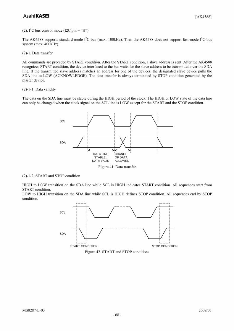
[AK4588]
MS0287-E-03 2009/05 - 68 -
(2). I2C bus control mode (I2C pin = “H”) The AK4588 supports standard-mode I2C-bus (max: 100kHz). Then the AK4588 does not support fast-mode I2C-bus system (max: 400kHz). (2)-1. Data transfer All commands are preceded by START condition. After the START condition, a slave address is sent. After the AK4588 recognizes START condition, the device interfaced to the bus waits for the slave address to be transmitted over the SDA line. If the transmitted slave address matches an address for one of the devices, the designated slave device pulls the SDA line to LOW (ACKNOWLEDGE). The data transfer is always terminated by STOP condition generated by the master device. (2)-1-1. Data validity The data on the SDA line must be stable during the HIGH period of the clock. The HIGH or LOW state of the data line can only be changed when the clock signal on the SCL line is LOW except for the START and the STOP condition.
SCL
SDA
DATA LINESTABLE :
DATA VALID
CHANGEOF DATAALLOWED
Figure 41. Data transfer
(2)-1-2. START and STOP condition HIGH to LOW transition on the SDA line while SCL is HIGH indicates START condition. All sequences start from START condition. LOW to HIGH transition on the SDA line while SCL is HIGH defines STOP condition. All sequences end by STOP condition.
SCL
SDA
STOP CONDITIONSTART CONDITION Figure 42. START and STOP conditions

[AK4588]
MS0287-E-03 2009/05 - 69 -
(2)-1-3. ACKNOWLEDGE ACKNOWLEDGE is a software convention used to indicate successful data transfers. The transmitting device will release the SDA line (HIGH) after transmitting eight bits. The receiver must pull down the SDA line during the acknowledge clock pulse so that that it remains stable “L” during “H” period of this clock pulse. The AK4588 will generates an acknowledge after each byte has been received. In the read mode, the slave, the AK4588 will transmit eight bits of data, release the SDA line and monitor the line for an acknowledge. If an acknowledge is detected and no STOP condition is generated by the master, the slave will continue to transmit data. If an acknowledge is not detected, the slave will terminate further data transmissions and await STOP condition. The register of ADC/DAC part can not generate acknowledge for READ operations.
SCL FROMMASTER
acknowledge
DATAOUTPUT BYTRANSMITTER
DATAOUTPUT BYRECEIVER
1 98
STARTCONDITION
Clock pulsefor acknowledge
not acknowledge
Figure 43. Acknowledge on the I2C-bus
(2)-1-4. FIRST BYTE The first byte, which includes seven bits of slave address and one bit of R/W bit, is sent after START condition. If the transmitted slave address matches an address for one of the device, the receiver who has been addressed pulls down the SDA line. The most significant five bits of the slave address are fixed as “00100”. The next two bits are CAD1 and CAD0 (device address bits). These two bits identify the specific device on the bus. The hard-wired input pins (CAD1 pin and CAD0 pin) set them. The eighth bit (LSB) of the first byte (R/W bit) defines whether a write or read condition is requested by the master. A “1” indicates that the read operation is to be executed. A “0” indicates that the write operation is to be executed.
0 0 1 0 0 CAD1 CAD0 R/W
(Regarding ADC/DAC part, register is set by CAD1/0 pins. “00” is inhibited to set for ADC/DAC.) (Fixed to “00” for DIR/DIT part)
Figure 44. The First Byte

[AK4588]
MS0287-E-03 2009/05 - 70 -
(2)-2. WRITE Operations Set R/W bit = “0” for the WRITE operation of the AK4588. After receipt the start condition and the first byte, the AK4588 generates an acknowledge, and awaits the second byte (register address). The second byte consists of the address for control registers of the AK4588. The format is MSB first, and those most significant 3-bits are “Don’t care”.
* * * A4 A3 A2 A1 A0
(*: Don’t care)
Figure 45. The Second Byte After receipt the second byte, the AK4588 generates an acknowledge, and awaits the third byte. Those data after the second byte contain control data. The format is MSB first, 8bits.
D7 D6 D5 D4 D3 D2 D1 D0
Figure 46. Byte structure after the second byte
The AK4588 is capable of more than one byte write operation by one sequence. After receipt of the third byte, the AK4588 generates an acknowledge, and awaits the next data again. The master can transmit more than one words instead of terminating the write cycle after the first data word is transferred. After the receipt of each data, the internal 5bits address counter is incremented by one, and the next data is taken into next address automatically. If the address exceed 1FH prior to generating the stop condition, the address counter will “roll over” to 00H and the previous data will be overwritten.
SDA
START
ACK
ACK
S
SlaveAddress
ACK
RegisterAddress(n) Data(n)
P
STOP
Data(n+x)
ACK
Data(n+1)
Figure 47. WRITE Operation

[AK4588]
MS0287-E-03 2009/05 - 71 -
(2)-3. READ Operations Set R/W bit = “1” for the READ operation of the AK4588. After transmission of a data, the master can read next address’s data by generating the acknowledge instead of terminating the write cycle after the receipt the first data word. After the receipt of each data, the internal 5bits address counter is incremented by one, and the next data is taken into next address automatically. If the address exceed 1FH prior to generating the stop condition, the address counter will “roll over” to 00H and the previous data will be overwritten. The AK4588 supports two basic read operations: CURRENT ADDRESS READ and RANDOM READ. ADC/DAC part register can not read. (2)-3-1. CURRENT ADDRESS READ The AK4588 has an internal address counter that maintains the address of the last word accessed, incremented by one. Therefore, if the last access (either a read or write) was to address “n”, the next CURRENT READ operation would access data from the address “n+1”. After receipt of the slave address with R/W bit set to “1”, the AK4588 generates an acknowledge, transmits 1byte data which address is set by the internal address counter and increments the internal address counter by 1. If the master does not generate an acknowledge to the data but generate the stop condition, the AK4588 discontinues transmission
SDA
START
ACK
ACK
S
SlaveAddress
ACK
Data(n) Data(n+1)
P
STOP
Data(n+x)
ACK
Data(n+2)
Figure 48. CURRENT ADDRESS READ
(2)-3-2. RANDOM READ Random read operation allows the master to access any memory location at random. Prior to issuing the slave address with the R/W bit set to “1”, the master must first perform a “dummy” write operation. The master issues start condition, slave address(R/W=“0”) and then the register address to read. After the register address’s acknowledge, the master immediately reissues start condition and the slave address with the R/W bit set to “1”. Then the AK4588 generates an acknowledge, 1byte data and increments the internal address counter by 1. If the master does not generate an acknowledge but generate the stop condition, the AK4588 discontinues transmission.
SDA
START
ACK
ACK
S S
START
SlaveAddress
WordAddress(n)
SlaveAddress
ACK
Data(n)
ACK
P
STOP
Data(n+x)
ACK
Data(n+1)
Figure 49. RANDOM READ

[AK4588]
MS0287-E-03 2009/05 - 72 -
SYSTEM DESIGN Figure 50 shows the system connection diagram. An evaluation board is available which demonstrates application circuits, the optimum layout, power supply arrangements and measurement results.
Condition: I2C serial control mode
TX1
INT1 1
AK4588
+10u
Audio DSP
2
3
4
5
6
7
8
9
10
11
60
59
58
57
56
55
54
53
52
51
50
BOUT
TVDD
DVDD
DVSS
TEST3
MCKO1
VOUT
BICK2
LRCK2
TEST1
NC
AVSS
AVDD
VREFH
VCOM
RIN
LIN
LOUT1
ROUT2
NC
80
79
78
77
76
75
74
73
72
71
70
TX0
MC
L K VIN
DAU
X2
I2C
RX
7
CA
D1
RX
4
PV
DD R
21
22
23
24
25
26
27
28
29
30
31
SD
A
DA
UX
1
SD
TI3
SD
TI2
SD
TI1
XTL
1
XTL
0
PD
N
DZF
2
DZF
1
LOU
T4
0.1u
S/PDIF sources S/PDIF out
(MPEG/AC3)
Analog 5V
Analog GroundDigital Ground
Digital 5V
Micro Controller
5
(Shi
eld)
+2.2u0.1u
12k
+
0.1u 10u +
X’tal
0.1u10u
C
C
12
13
14
15
16
69
68
67
66
65
32
33
34
35
36
49
48
47
46
45
SDTO2
UOUT
MCKO2
COUT
XTO
XTI
SC
L
CS
N
SD
TI4
MA
STE
R
NC
NC
NC
ROUT1
RX0
RX1
TEST
2
CA
D0
RX
5
RX6
INT0
MUTE
(Shield)
SDTO1
LRCK1
CDTO
17
18
19
20
BICK1
NC
LOU
T3
NC
37
38
39
40
RO
UT4
LOUT2
ROUT3
NC
44
43
42
41
NC
RX
3
NC
RX
2
64
63
62
61
PVS
S
+ 3.3V to 5V
Digital
Audi
o D
SP
(MPE
G/A
C3)
(Mic
ro
Con
trolle
r)
Audio DSP(MPEG/AC3) Micro Controller
MU
TE
MU
TE
MU
TE
(Shi
eld)
(Shi
eld)
(Shi
eld)
MUTE
MUTE
MUTE
MUTE
(Shield)
(Shield)
(Shield)
(Shield)
(Shield)
(S/P
DIF
So
urce
)
(S/PDIF sources)
Micro Controller
Figure 50. Typical Connection Diagram
Notes: - “C” depends on the crystal. - AVSS, DVSS and PVSS must be connected the same analog ground plane. - Digital signals, especially clocks, should be kept away from the R pin in order to avoid an effect to the clock jitter
performance. - In case of coaxial input, ground of RCA connector and terminator should be connected to PVSS of the AK4588
with low impedance on PC board.

[AK4588]
MS0287-E-03 2009/05 - 73 -
1. Grounding and Power Supply Decoupling The AK4588 requires careful attention to power supply and grounding arrangements. AVDD, DVDD, PVDD and TVDD are usually supplied from analog supply in system. Alternatively if AVDD, DVDD, PVDD and TVDD are supplied separately, the power up sequence is not critical. AVSS, DVSS and PVSS of the AK4588 must be connected to analog ground plane. System analog ground and digital ground should be connected together near to where the supplies are brought onto the printed circuit board. Decoupling capacitors should be as near to the AK4588 as possible, with the small value ceramic capacitor being the nearest. 2. Voltage Reference Inputs The voltage of VREFH sets the analog input/output range. The VREFH pin is normally connected to AVDD with a 0.1μF ceramic capacitor. VCOM is a signal ground of this chip. An electrolytic capacitor 2.2μF parallel with a 0.1μF ceramic capacitor attached to the VCOM pin eliminates the effects of high frequency noise. No load current may be drawn from the VCOM pin. All signals, especially clocks, should be kept away from the VREFH and VCOM pins in order to avoid unwanted coupling into the AK4588. 3. Analog Inputs ADC inputs are single-ended and internally biased to VCOM. The input signal range scales with the supply voltage and nominally 0.62 x VREFH Vpp (typ). The ADC output data format is 2’s complement. The DC offset is removed by the internal HPF. The AK4588 samples the analog inputs at 64fs. The digital filter rejects noise above the stop band except for multiples of 64fs. The AK4588 includes an anti-aliasing filter (RC filter) to attenuate a noise around 64fs. 4. Analog Outputs The analog outputs are also single-ended and centered around the VCOM voltage. The input signal range scales with the supply voltage and nominally 0.6 x VREFH Vpp. The DAC input data format is 2’s complement. The output voltage is a positive full scale for 7FFFFFH(@24bit) and a negative full scale for 800000H(@24bit). The ideal output is VCOM voltage for 000000H(@24bit). The internal analog filters remove most of the noise generated by the delta-sigma modulator of DAC beyond the audio passband. DC offsets on analog outputs are eliminated by AC coupling since DAC outputs have DC offsets of a few mV.
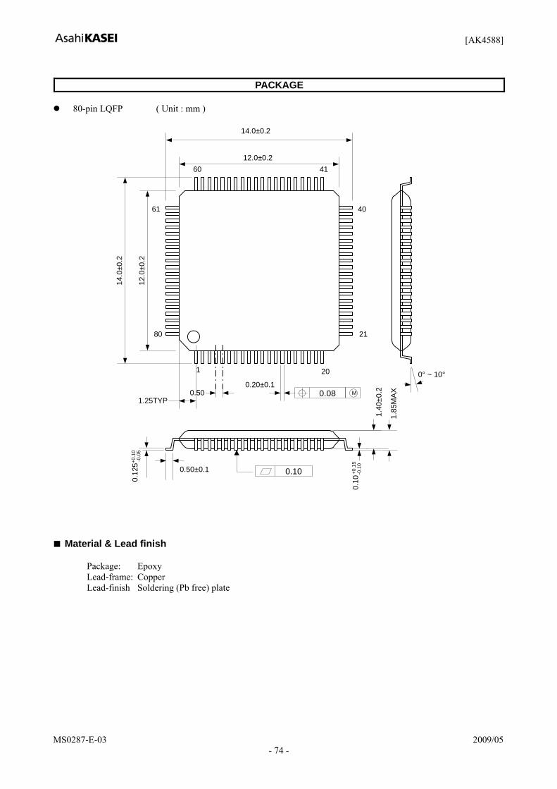
[AK4588]
MS0287-E-03 2009/05 - 74 -
PACKAGE
80-pin LQFP ( Unit : mm )
14
.0±0
.2
12.0
±0.2
0.50
1 20
21
40
4160
61
80
12.0±0.2
14.0±0.2
1.25TYP0.08 M
0.12
5+0.1
0
-0.0
5
0.50±0.1
1.85
MA
X
0.10
+0.
15
-0.1
0
1.40
±0.2
0.10
0.20±0.10° ~ 10°
■ Material & Lead finish
Package: Epoxy Lead-frame: Copper Lead-finish Soldering (Pb free) plate

[AK4588]
MS0287-E-03 2009/05 - 75 -
MARKING
AK4588VQ
XXXXXXX
1) Pin #1 indication 2) Date Code: XXXXXXX(7 digits) 3) Marking Code: AK4588VQ 4) Asahi Kasei Logo
REVISION HISTORY Date (YY/MM/DD) Revision Reason Page Contents 04/01/22 00 First Edition 04/03/18 01 Error Correct 12 ADC Digital Filter, Group Delay: 19.1/fs → 16/fs 08/05/22 02 Spec Change Ambient Temperature range was changed.
“-10 ∼ +70°C” → “-40 ∼ +85°C” 09/05/25 03 Error Correct 9 ■ Handling of Unused Pin
The treatment of TEST3 pin was changed. (to DVSS)

[AK4588]
MS0287-E-03 2009/05 - 76 -
IMPORTANT NOTICE
These products and their specifications are subject to change without notice. When you consider any use or application of these products, please make inquiries the sales office of Asahi Kasei EMD Corporation (AKEMD) or authorized distributors as to current status of the products.
AKEMD assumes no liability for infringement of any patent, intellectual property, or other rights in the application or use of any information contained herein.
Any export of these products, or devices or systems containing them, may require an export license or other official approval under the law and regulations of the country of export pertaining to customs and tariffs, currency exchange, or strategic materials.
AKEMD products are neither intended nor authorized for use as critical componentsNote1) in any safety, life support, or other hazard related device or systemNote2), and AKEMD assumes no responsibility for such use, except for the use approved with the express written consent by Representative Director of AKEMD. As used here:
Note1) A critical component is one whose failure to function or perform may reasonably be expected to result, whether directly or indirectly, in the loss of the safety or effectiveness of the device or system containing it, and which must therefore meet very high standards of performance and reliability. Note2) A hazard related device or system is one designed or intended for life support or maintenance of safety or for applications in medicine, aerospace, nuclear energy, or other fields, in which its failure to function or perform may reasonably be expected to result in loss of life or in significant injury or damage to person or property.
It is the responsibility of the buyer or distributor of AKEMD products, who distributes, disposes of, or otherwise places the product with a third party, to notify such third party in advance of the above content and conditions, and the buyer or distributor agrees to assume any and all responsibility and liability for and hold AKEMD harmless from any and all claims arising from the use of said product in the absence of such notification.


![AK9754AE English Datasheet · [AK9754] 018006915-E-00 2018/06-4-5.Pin Configurations and Functions 5.1.Pin Configurations 4 1 2 3 8 7 6 5 VSS VDD CAD0 CAD1 SCL SDA INTN SYNC SCL SDA](https://img.pdfslide.net/doc/110x75/601ad8b72a6c616e353f1c33/ak9754ae-english-datasheet-ak9754-018006915-e-00-201806-4-5pin-configurations.jpg)
![CLRC663 High performance NFC reader solutionNXP Semiconductors CLRC663 High performance NFC reader solution 4. Quick reference data Table 1. Quick reference data [1] VDD(PVDD) must](https://img.pdfslide.net/doc/110x75/600818bf432e5007cb118bfb/clrc663-high-performance-nfc-reader-nxp-semiconductors-clrc663-high-performance.jpg)