Embed Size (px)
Citation preview
8/18/2019 Akai Lcd Tv Lct3201td_service Masnual
http://slidepdf.com/reader/full/akai-lcd-tv-lct3201tdservice-masnual 1/108

8/18/2019 Akai Lcd Tv Lct3201td_service Masnual
http://slidepdf.com/reader/full/akai-lcd-tv-lct3201tdservice-masnual 2/108
Model:
LCT3201TD Safety Instructions.......................................................................1~2Production specification...........................................................3~11 DVD Player's Spec. for LCD Comb..............................................12
LCD COMBO Connection............................................................13
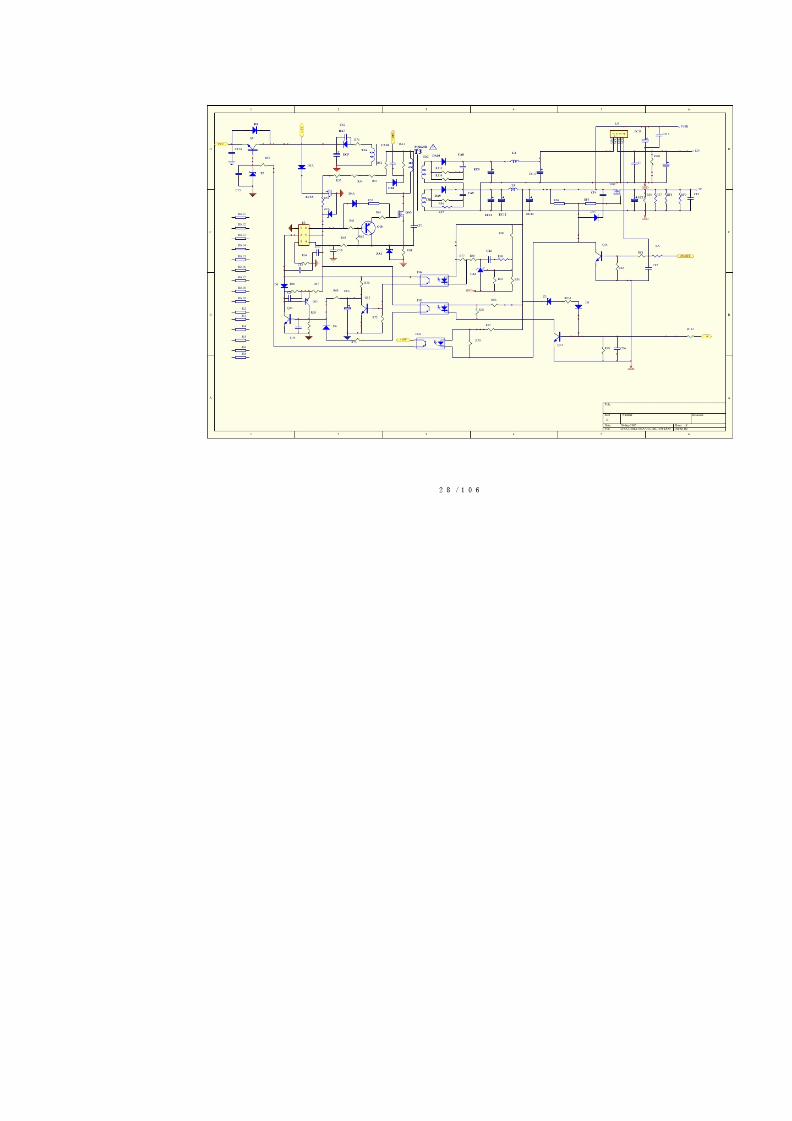
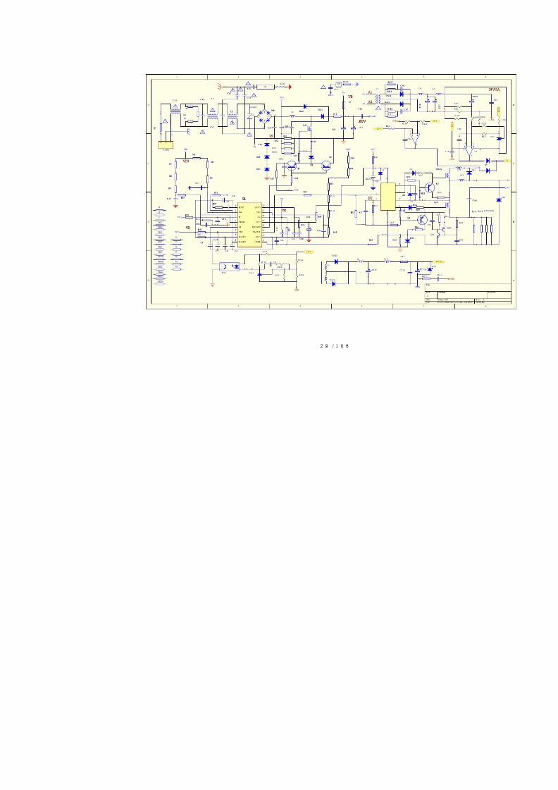
Panel Inverter Power..............................................................14~29
Basic Operations & Circuit Description..................................... ..30
PCB Function........................................................................... .. 31
PCB Failure Analysis................................................................
. 32
Basic Operation of LCD-TV...................................................33~34
IC Descriptions..................................................................... .35~45
LCD Panel specification........................................................ 46~101
Exploded View Diagram.............................................................. 102
Spare parts list.....................................................................103~104
V-Chip Password....................................................................... 105
Software Upgrade................................................................105~106
SERVICE MANUAL
This manual is the latest at the time of printing, and does notinclude the modification which may be made after the printing,
by the constant improvement of product.
8/18/2019 Akai Lcd Tv Lct3201td_service Masnual
http://slidepdf.com/reader/full/akai-lcd-tv-lct3201tdservice-masnual 3/108
I. Safety Instructions
PRECAUTIONS DURING SERVICING
1. In addition to safety, other parts and assemblies are
specified for conformance with such regulations as
those applying to spurious radiation. These must
also be replaced only with specified replacements.
Examples: RF converters, tuner units, antenna
selection switches, RF cables, noise-blocking
capacitors, noise-blocking filters, etc.
2. Use specified internal Wiring. Note especially:
1) Wires covered with PVC tubing
2) Double insulated wires
3) High voltage leads
3. Use specified insulating materials for hazardous
live parts. Note especially:
1) Insulating Tape
2) PVC tubing
3) Spacers (insulating bar riers)
4) Insulating sheets for transistors5) Plastic screws for fixing micro switches
4. When replacing AC primary side components
(transformers, power cords, noise blocking
capacitors, etc.), wrap ends of wires securely about
the terminals before soldering.
5. Make sure that wires do not contact heat generating
parts (heat sinks, oxide metal film resistors, fusible
resistors, etc.)
6. Check if replaced wires do not contact sharply edged
or pointed pa rts.
7. Make sure that foreign objects (screws, solder
droplets, etc.) do not remain inside the set.
MAKE YOUR CONTRIBUTION TO PROTECT THE
ENVIRONMENT
Used batteries with the ISO symbol
for recycling as well as small
accumulators (rechargeable batteries), mini-batteries
(cells) and starter batteries should not be thrown
into the garbage can.
Please leave them at an appropriate depot
WARNING:
Before servicing this TV receiver, read the X-RAY
RADIATION PRECAUTION, SAFETY INSTRUCTION
and PRODUCT SAFETY NOTICE.
X-RAY RADIATION PRECAUTION
1. Excessively high can produce potentially hazardous
X-RAY RADIATION. To avoid such hazards, the high
voltage must not exceed the specified limit. The
normal value of the high voltage of this TV receiver
is 2 7 KV at zero b ean current (minimum b rightness).
The high voltage must not exceed 30 KV under any
circumstances. Each time when a receiver requires
servicing, the high voltage should be checked. The
reading of the high voltage is recommended to be
recorded as a part of the service record, It is
important to use an accurate and reliable highvoltage meter.
2. The only source of X-RAY RADIATION in this TV
receiver is the picture tube. For con tinued X-RAY
RADIATION protection, the replacement tube must be
exactly the same type as specified in the parts list.
3. Some parts in this TV receiver have special safety
related characteristics for X-RADIATION protection.
For continued safety, the parts replacement should
be under taken only after referring the PRODUCT
SAFETY NOTICE.
SAFETY INSTRUCTION
The service should not be attempted by anyone
unfamiliar with the necessary instructions on this TV
receiver. The following are the necessary instructions
to be observed before servicing.
1. An isolation transformer should be connected in the
power line between the receiver and the AC line
when a service is performed on the primary of the
converter transformer of the set.
2. Comply with all caution and safety related provided
on the back of the cabinet, inside the cabinet, on the
chassis or picture tube.
3. To avoid a shock hazard, always discharge the
picture tube's anode to the chassis ground before
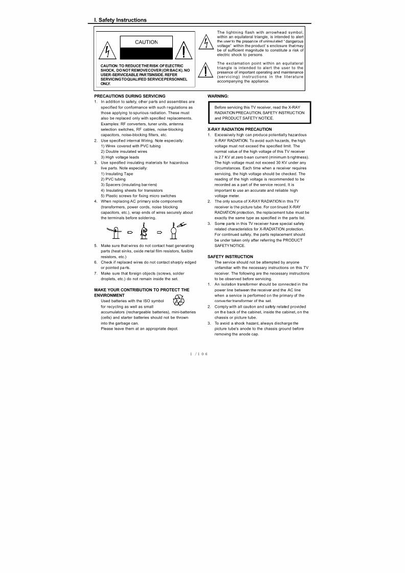
The lightning flash with arrowhead symbol,within an equilateral triangle, is intended to alertthe user to the presence of uninsulated “dangerousvoltage” within the product’ s enclosure that maybe of sufficient magnitude to constitute a risk of electric shock to persons.
The exclamation point within an equilateraltriangle is intended to alert the user to thepresence of important operating and maintenance(serv ic ing) inst ruct ions in the l i teratureaccompanying the appliance.
CAUTION: TO REDUCE THE RISK OF ELECTRICSHOCK, DO NOT REMOVE COVER (OR BACK). NOUSER-SERVICEABLE PARTSINSIDE. REFER
SERVICING TO QUALIFIED SERVICE PERSONNELONLY.
CAUTION
RISK OF ELECTRIC SHOCKDO NOT O PEN
8/18/2019 Akai Lcd Tv Lct3201td_service Masnual
http://slidepdf.com/reader/full/akai-lcd-tv-lct3201tdservice-masnual 4/108
PRODUCT SAFETY NOTICE
Many electrical and mechanical parts in this TV
receiver have special safety-related characteristics.
These characteristics are offer passed unnoticed by
visual spection and the protection afforded by them
cannot necessarily be obtained by using replacement
components rates for a higher voltage, wattage, etc.
The replacement parts which have these specialsafety characteristics are identified by marks on
the schematic diagram and on the parts list.
Before replacing any of these components, read the
parts list in this manual carefully. The use of
substitute replacement parts which do not have the
same safety characteristics as specified in the parts
list may create shock, fire, X-RAY RADIATION or
other hazards.
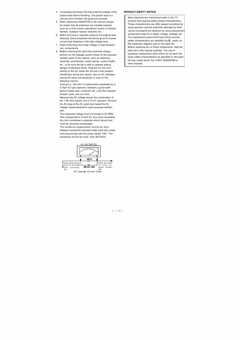
Good earth ground
such as the water
pipe, conductor,
etc.
Place this probe
o n e a c h e x -
posed metallic
part
AC VOLTMETER
AC Leak age Current Check
4. Completely discharge the high potential voltage of the
picture tube before handling. The picture tube is a
vacuum and if broken, the gl ass will explode.
5. When replacing a MAIN PCB in the cabinet, always
be certain that all protective are installed properly
such as co ntrol knobs, adjustment covers o r shields,
barriers, isolation resistor networks etc.
6. When servicing is required, observe the original lead
dressing. Extra precaution sho uld be gi ven to a ssure
correct lead dressing in the high voltage area.
7. Keep wires away from high voltage or high tempera
ture components.
8. Before returning the set to the customer, always
perform an AC leakage current check on the exposed
metallic parts of the cabinet, such as antennas,
terminals, screwheads, metal overlay, control shafts,
etc., to be sure the set is safe to operate without
danger of electrical shock. Plug the AC line cord
directly to the AC outlet (do not use a line isolation
transformer during this check). Use an AC voltmeter having 5K ohms volt sensitivity or more in the
following manner.
Connect a 1.5K ohm 10 watt resistor paralleled by a
0.15µF AC type capacitor, between a good earth
ground (water pipe, conductor etc.,) and the exposed
metallic parts, one at a time.
Measure the AC voltage across the combination of
the 1.5K ohm resistor and 0.15 uF capacitor. Reverse
the AC plug at the AC outlet and repeat the AC
voltage measurements for each exposed metallic
part.
The measured voltage must not exceed 0.3V RMS.
This corresponds to 0.5mA AC. Any value exceeding
this limit constitutes a potential shock hazard and
must be corrected immediately.
The resistance measurement should be done
between accessible exposed metal parts and power
cord plug prongs with the power switch "ON". The
resistance should be more than 6M ohms.
8/18/2019 Akai Lcd Tv Lct3201td_service Masnual
http://slidepdf.com/reader/full/akai-lcd-tv-lct3201tdservice-masnual 5/108
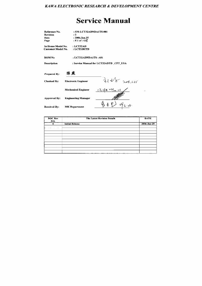
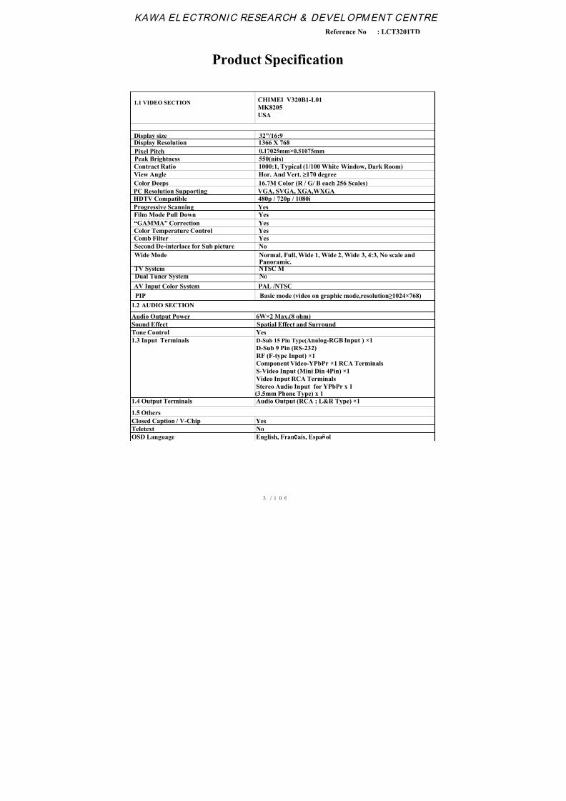
KAWA ELECTRONIC RESEARCH & DEVELOPMENT CENTRE
Reference No : LCT3201TD
Product Specification
CHIMEI V320B1-L01
MK8205
USA
1.1 VIDEO SECTION
Display size 32”/16:9Display Resolution 1366 X 768
Pixel Pitch 0.17025mm×0.51075mm
Peak Brightness 550(nits)
Contract Ratio 1000:1, Typical (1/100 White Window, Dark Room)
View Angle Hor. And Vert. ≥170 degreeColor Deeps 16.7M Color (R / G/ B each 256 Scales)
PC Resolution Supporting VGA, SVGA, XGA,WXGA
HDTV Compatible 480p / 720p / 1080i
Progressive Scanning Yes
Film Mode Pull Down Yes
“GAMMA” Correction Yes
Color Temperature Control Yes
Comb Filter Yes
Second De-interlace for Sub picture No
Wide Mode Normal, Full, Wide 1, Wide 2, Wide 3, 4:3, No scale andPanoramic.
TV System NTSC M
Dual Tuner System No
AV Input Color System PAL /NTSC
PIP Basic mode (video on graphic mode,resolution≥1024×768)
1.2 AUDIO SECTION
Audio Output Power 6W×2 Max.(8 ohm)
Sound Effect Spatial Effect and Surround
Tone Control Yes
1.3 Input Terminals D-Sub 15 Pin Type(Analog-RGB Input ) ×1
D-Sub 9 Pin (RS-232)
RF (F-type Input) ×1Component Video-YPbPr ×1 RCA Terminals
S-Video Input (Mini Din 4Pin) ×1
Video Input RCA Terminals
Stereo Audio Input for YPbPr x 1 (3.5mm Phone Type) x 1
1.4 Output Terminals Audio Output (RCA ; L&R Type) ×1
1.5 Others
Closed Caption / V-Chip Yes
Teletext No
OSD Language English, Fran ais, Espa ol
8/18/2019 Akai Lcd Tv Lct3201td_service Masnual
http://slidepdf.com/reader/full/akai-lcd-tv-lct3201tdservice-masnual 6/108
KAWA ELECTRONIC RESEARCH & DEVELOPMENT CENTRE
Reference No : LCT3201TD
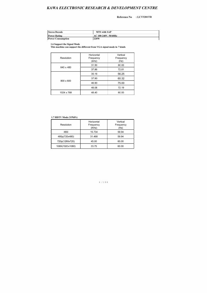
Stereo Decode MTS with SAP Power Rating AC 100-240V, 50/60Hz
Power Consumption 220W
1.6 Support the Signal Mode
This machine can support the different from VGA signal mode in 7 kinds
1.7 HDTV Mode (YPbPr)
Resolution
Horizontal
Frequency
(kHz)
Vertical
Frequency
(Hz)
640 x 48031.50 60.00
37.86 72.81
800 x 600
35.16 56.25
37.90 60.32
46.90 75.00
48.08 72.19
1024 x 768 48.40 60.00
Resolution
Horizontal
Frequency
(KHz)
Vertical
Frequency
(Hz)
480i 15.734 59.94
480p(720x480) 31.468 59.94
720p(1280x720) 45.00 60.00
1080i(1920x1080) 33.75 60.00
8/18/2019 Akai Lcd Tv Lct3201td_service Masnual
http://slidepdf.com/reader/full/akai-lcd-tv-lct3201tdservice-masnual 7/108
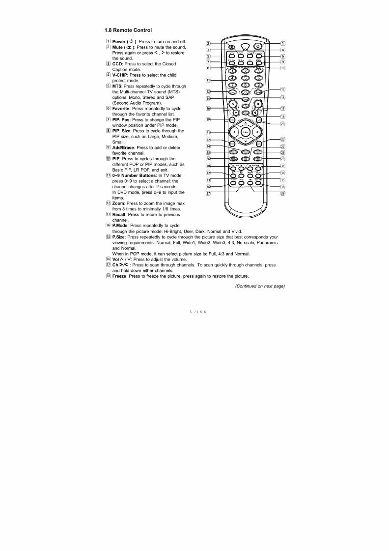
1.8 Remote Control
Power ( ): Press to turn on and off.
Mute ( ): Press to mute the sound.
Press again or press , to restore
the sound.
CCD: Press to select the Closed
Caption mode.
V-CHIP: Press to select the child
protect mode.
MTS: Press repeatedly to cycle through
the Multi-channel TV sound (MTS)
options: Mono, Stereo and SAP
(Second Audio Program).
Favorite: Press repeatedly to cycle
through the favorite channel list.
PIP. Pos: Press to change the PIPwindow position under PIP mode.
PIP. Size: Press to cycle through the
PIP size, such as Large, Medium,
Small.
Add/Erase: Press to add or delete
favorite channel.
PIP: Press to cycles through the
different POP or PIP modes, such as
Basic PIP, LR POP, and exit.
0~9 Number Buttons: In TV mode,
press 0~9 to select a channel; thechannel changes after 2 seconds.
In DVD mode, press 0~9 to input the
items.
Zoom: Press to zoom the image max
from 8 times to minimally 1/8 times.
Recall: Press to return to previous
channel.
P.Mode: Press repeatedly to cycle
(Continued on next page)
through the picture mode: Hi-Bright, User, Dark, Normal and Vivid.
P.Size: Press repeatedly to cycle through the picture size that best corresponds your
viewing requirements: Normal, Full, Wide1, Wide2, Wide3, 4:3, No scale, Panoramicand Normal.
When in POP mode, it can select picture size is: Full, 4:3 and Normal.
Vol / : Press to adjust the volume.
Ch / : Press to scan through channels. To scan quickly through channels, press
and hold down either channels.
Freeze: Press to freeze the picture, press again to restore the picture.

8/18/2019 Akai Lcd Tv Lct3201td_service Masnual
http://slidepdf.com/reader/full/akai-lcd-tv-lct3201tdservice-masnual 8/108
Menu: Press to enter into the on-screen
setup menu, press again to exit.
S.Mode: Press repeatedly to cycle
through the sound mode: Normal,
News, Cinema, Flat and User. , , , , Enter : Press , , ,
to move the on-screen cursor. To
select an item, press ENTER to
confirm. And it can also press or
to scan through channels, press
or to adjust the volume excepting
DVD mode.
System: Press repeatedly to cycle
through the system options: AUTO
and NTSC3.58.
(This button is inactive for TV, VGA,COMPONENT input source.)
Source: Press to select the signal
source, such as TV, AV, S-Video,
Component, DVD or VGA.
Sleep: Press repeatedly until it
displays the time in minutes (5 Min,
10 Min, 15 Min, 30 Min, 60 Min, 90
Min, 120 Min and, OFF) that you
want the TV to remain on before
shutting off. To cancel sleep time,
press Sleep button repeatedlyuntil sleep OFF appears.
Display: Press to display the channel
information and it disappear after 3
seconds.
Play/Pause: Press to play or pause
the DVD disc.
Stop: Press to stop playing the disc.
Angle: Press to select desired viewing
angle of the Video (disc feature).
Open/Close: Press to open or close
the disc tray.
(Continued on next page)
Skip+/-: Press to skip the forward or backward.
Search+/- : Press to search the forward or backward.
DVD Menu: Press to return DVD disc menu.
8/18/2019 Akai Lcd Tv Lct3201td_service Masnual
http://slidepdf.com/reader/full/akai-lcd-tv-lct3201tdservice-masnual 9/108
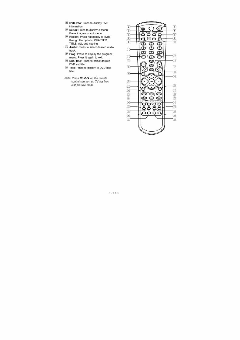
DVD Info: Press to display DVD
information.
Setup: Press to display a menu.
Press it again to exit menu.
Repeat: Press repeatedly to cyclethrough the options: CHAPTER,
TITLE, ALL and nothing.
Audio: Press to select desired audio
track.
Prog: Press to display the program
menu. Press it again to exit.
Sub. title: Press to select desired
DVD subtitle.
Title: Press to display to DVD disc
title.
Note: Press Ch / on the remote
control can turn on TV set from
last preview mode.
l
.
8/18/2019 Akai Lcd Tv Lct3201td_service Masnual
http://slidepdf.com/reader/full/akai-lcd-tv-lct3201tdservice-masnual 10/108
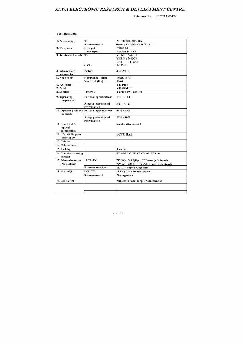
KAWA ELECTRONIC RESEARCH & DEVELOPMENT CENTRE
Reference No : LCT32ADTD
Technical Data
TV AC 100-240, 50/ 60Hz1. Power supply
Remote control Battery 3V (UM-3/R 6P/AA×2)
RF input NTSC M2. TV system
Video input PAL/NTSC 3.58
TV VHF-L : 2~6CH
VHF-H : 7~13CH
UHF : 14~69CH
3. Receiving channels
CATV 1~125CH
4. Intermediate
frequencies
Picture 45.75MHz
5 . Sca nni ng Hor izo nta l (Hz ) 15625/15750
Ver tic al (Hz ) 50/60
6 . AC plug UL Plug
7. Panel V320B1-L01
8. Speaker Internal 8 ohm 10W (max) ×2
9. Operating
temperature
Fulfill all specifications 15 C ~ 30 C
Accept picture/sound
reproduction
5 C ~ 33 C
10. Operating relative
humidity
Fulfill all specifications 45% ~ 75%
Accept picture/sound
reproduction
20% ~ 80%
11. Electrical &
optical
specification
See the attachment 1.
12. Circuit diagram
drawing No.LCT32HAB
13. Cabinet
14. Cabinet color
15. Packing 1 set per
16. Container stuffing
method
RD/05/P/LC26HAB/CSI/02 REV: 01
17. Dimension (mm) LCD-TV 799(W) 569.7(H) 107(D)mm (w/o Stand)
(No packing) 799(W) 635.8(H) 267.5(D)mm (with Stand)
Remote control unit 183(L) 53(W) 28(T)mm
18. Net weight LCD-TV 18.8Kg (with Stand) approx.
Remote control 70g (approx.)
19. Cell Defect Subject to Panel supplier specification
8/18/2019 Akai Lcd Tv Lct3201td_service Masnual
http://slidepdf.com/reader/full/akai-lcd-tv-lct3201tdservice-masnual 11/108
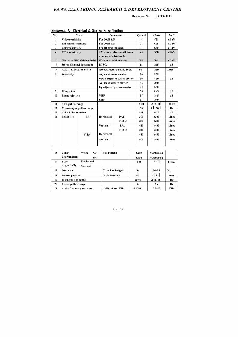
KAWA ELECTRONIC RESEARCH & DEVELOPMENT CENTRE
Reference No : LCT3201TD
Attachment 1 Electrical & Optical Specification
No. Items Instruction Typical Limit Unit
1 Video sensitivity For 30dB S/N 44 51 dBuV
2 FM sound sensitivity For 30dB S/N 21 35 dBuV
3 Color sensitivity For RF transmission 37 40 dBuV
4 CCD sensitivity TV screen refreshes 40 times
number of mistakes 8
43 50 dBuV
5 Minimum NICAM threshold Without crackline noise N/A N/A dBuV
6 Stereo Channel Separation BTSC. 18 ≥15 dB
7 AGC static characteristic Accept. Picture/Sound repr. 90
≥90
dBuV
8 Selectivity Adjacent sound carrier 30≥
28
Below adjacent sound carrier 30 ≥30 dB
Adjacent picture carrier 45 ≥40
Up adjacent picture carrier 40 ≥30
9 IF rejection 55 ≥45 dB
10 Image rejection VHF 57 ≥45 dB
UHF 55 ≥40
11 AFT pull-in range ±1.0 ≥±1.0 MHz
12 Chroma sync pull-in range ±500 ≥±200 Hz
13 Color killer function -11 -10 dB
PAL 300 ≥300 LinesHorizontal
NTSC 260 ≥240 Lines
PAL 410 ≥400 Lines
RF
Vertical
NTSC 320 ≥300 Lines
Horizontal 450 ≥450 Lines
14 Resolution
Video
Vertical 400 ≥400 Lines
XW 0.295 0.295±0.0215 Color
Coordination
White
YW
Full Pattern
0.300 0.300±0.02
Horizontal16 View
Angle(Lo/3) Vertical
170 ≥170 Degree
17 Overscan Cross hatch signal 96 94~98 %
18 Picture position In all direction ±2 ±3 mm
19 H sync pull-in range ±400 ≥±200 Hz
20 V sync pull-in range 6 ≥6 Hz
21 Audio frequency response ±3dB ref. to 1KHz 0.15~12 0.2~12 KHz

8/18/2019 Akai Lcd Tv Lct3201td_service Masnual
http://slidepdf.com/reader/full/akai-lcd-tv-lct3201tdservice-masnual 12/108
KAWA ELECTRONIC RESEARCH & DEVELOPMENT CENTRE
Reference No : LCT3201TD
22 Max Audio Output Power 7×2 ≥5.0×2 W
23 Audio output power
10% THD
1KHz 10% THD 6×2 ≥4.0×2 W
24 THD Po=0.5W 0.5 3 %
25 Signal to buzz ratio coeighting 50 ≥30 dB
26 Minimum volume hum coeighting 6 10 mVrms
27 Maximum woofer output power N/A N/A W
28 Woofer audio frequency
response
±3dB ref. to 15Hz AV
mode
N/A N/A Hz
29 Tone low frequency 100Hz ref. to 1KHz
AV mode±
8≥±
3
dB
30 Tone high frequency 10KHz ref. to 1KHz
AV mode
±8 ≥±3 dB
31 Balance Center 0 ±2
Max. 3 2 dB
Min. -35 -30
32 Video input level 1.0 1±0.3 Vpp
33 Audio input level*
1
1.0 * 0.5±
0.3 Vrms
34 Video output level N/A N/A Vrms
35 Audio output level* 2 0.3 * 0.5±0.3 Vrms
36 AV Audio input max. level 2 2 Vrms
37 AV Audio output L/R
Separation
35 ≥30 dB
Operating 200 200 W38 Power consumpution
Stand by 3 5 W
39 IR receiving distance 0 Degree 7 ≥6 m
left/right 60 ≥45 Degree40 IR receiving
angle Up/down
5m
20 ≥15 Degree
41 Dielectric strength DC 3KV 1min. 5 10 mArms
42 The vibration noise from
electromagnetic devices in LCD-
TV set
The distance between
the tester and the
LCD-TV set is four
times as many as the
screen height
No obvious vibration noise can be
heard
8/18/2019 Akai Lcd Tv Lct3201td_service Masnual
http://slidepdf.com/reader/full/akai-lcd-tv-lct3201tdservice-masnual 13/108
KAWA ELECTRONIC RESEARCH & DEVELOPMENT CENTRE
Reference No : LCT3201TD
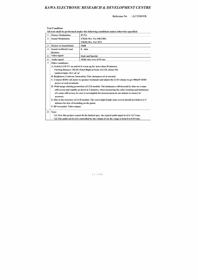
Test Condition
All tests shall be performed under the following conditions unless otherwise specified
1 Picture Modulation 87.5%
2 Sound Modulation 27KHz Dev. For DK/I/BG
15KHz Dev. For M/N
3 Picture to Sound Ratio 10dB
4 Sound Artificial Load
Resistor
8 ohm
5 Video signal Stair and Special
6 Audio signal 1KHz sine wave 0.5Vrms
7 Other conditions:
A. Switch LCD-TV on and let it warm up for more than 30 minutes.
Viewing distance: 3H (H: Panel High) in front of LCD, about 2M.
Ambient light: 0.1 cd/ m2
B. Brightness, Contrast, Saturation, Tint, sharpness set at normal.
C. Connect RMS volt meter to speaker terminals and adjust the LCD volume to get 500mW RMS
power at each terminals.
D. With image sticking protection of LCD module. The luminance will descend by time on a same
still screen and rapidly go down in 5 minutes, when measuring the color tracking and luminance
of a same still screen, be sure to accomplish the measurement in one minute to ensure its
accuracy.
E. Due to the structure of LCD module. The extra-high-bright same screen should not hold over 5
minutes for fear of branding on the panel.
F. RF test point: Video output.
8 Note:
*(1) Now this project cannot fit the limited spec. the typical audio input level is 1.0 Vrms,
*(2) The audio out level is controlled by the volume level, the range is from 0 to 0.5Vrms.
8/18/2019 Akai Lcd Tv Lct3201td_service Masnual
http://slidepdf.com/reader/full/akai-lcd-tv-lct3201tdservice-masnual 14/108
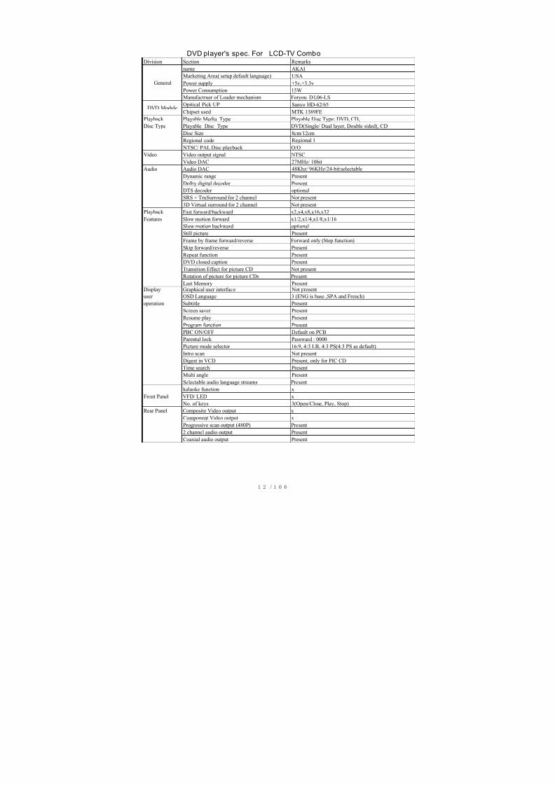
DVD player's spec. For LCD-TV ComboDivision Section Remarks
name AKAI
Marketing Area( setup default language) USA
Power supply +5v,+3.3v
Power Consumption 15W
Manufactruer of Loader mechanism Foryou D L06-LS
Opitical Pick UP Sanyo HD-62/65
Chipset used MTK 1389FE
Playback Playable Media Type Playable Disc Type: DVD, CD,
Disc Type Playable Disc Type DVD(Single/ Dual layer, Double sided), CD
Disc Size 8cm/12cm
Regional code Regional 1
NTSC/ PAL Disc playback O/O
Video Video output signal NTSC
Video DAC 27MHz/ 10bit
Audio Audio DAC 48Khz/ 96KHz/24-bit:selectable
Dynamic range Present
Dolby digital decoder Present
DTS decoder optional
SRS + TruSurround for 2 channel Not present
3D Virtual surround for 2 channel Not present
Playback Fast forward/backward x2,x4,x8,x16,x32
Features Slow motion forward x1/2,x1/4,x1/8,x1/16
Slow motion backward optional
Still picture Present
Frame by frame forward/reverse Forward only (Step function)
Skip forward/reverse Present
Repeat function Present
DVD closed caption Present
Transition Effect for picture CD Not present
Rotation of picture for picture CDs Present
Last Memory PresentDisplay Graphical user interface Not present
user OSD Language 3 (ENG is base ,SPA and French)
operation Subtitle Present
Screen saver Present
Resume play Present
Program function Present
PBC ON/OFF Default on PCB
Parental lock Passward : 0000
Picture mode selector 16:9, 4:3 LB, 4:3 PS(4:3 PS as default)Intro scan Not present
Digest in VCD Present, only for PIC CD
Time search Present
Multi angle Present
Selectable audio language streams Present
kalaoke function x
Front Panel VFD/ LED x
No. of keys 3(Open/Close, Play, Stop)
Rear Panel Composite Video output x
Component Video output x
Progressive scan output (480P) Present
2 channel audio output PresentCoaxial audio output Present
General
DVD Module
8/18/2019 Akai Lcd Tv Lct3201td_service Masnual
http://slidepdf.com/reader/full/akai-lcd-tv-lct3201tdservice-masnual 15/108
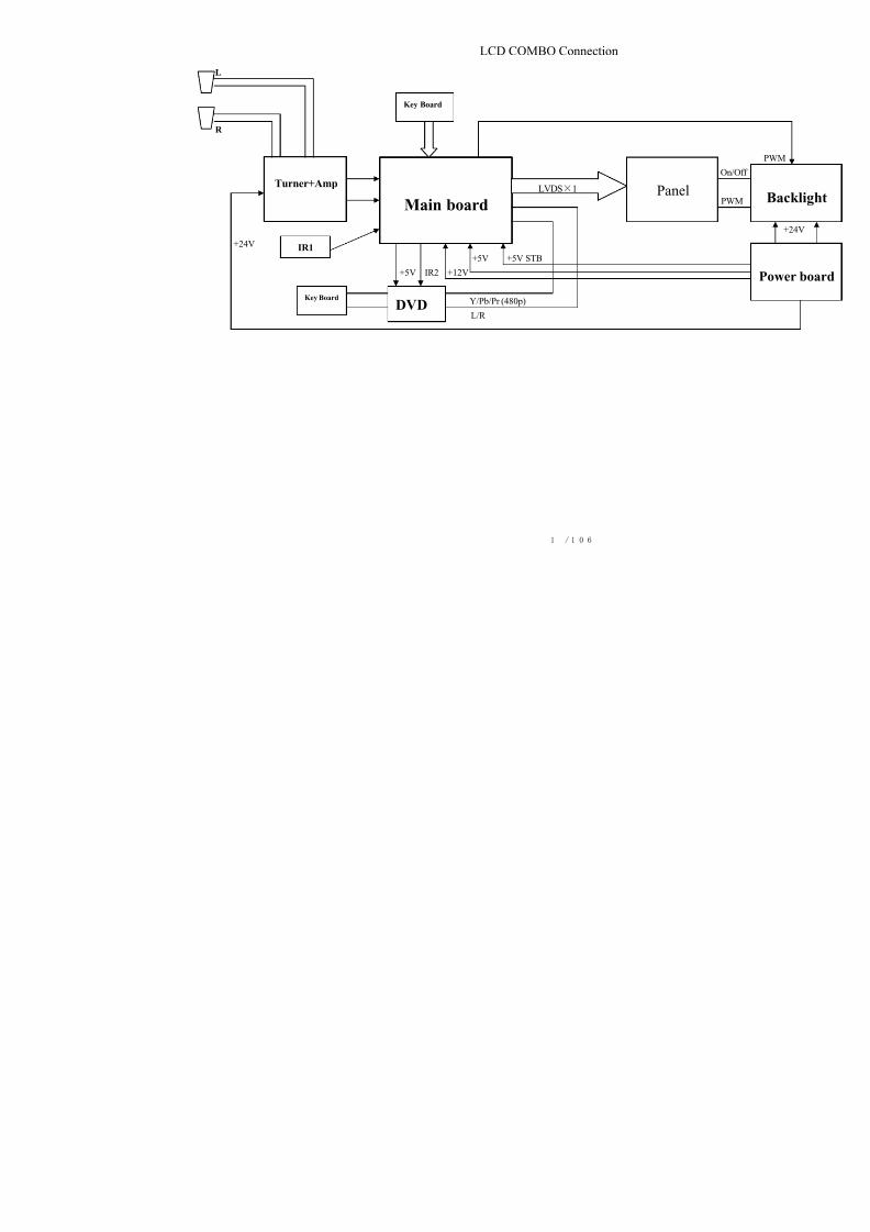
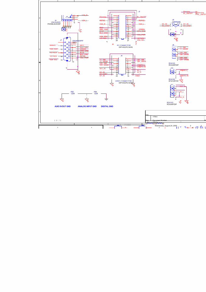
LCD COMBO Connection
L
R
+24V
+5V +5V STB
+5V IR2 +12V
Y/Pb/Pr (480p)
L/R
Turner+Amp
Main boardPan
DVDKey Board
IR1
Key Board
LVDS×1
8/18/2019 Akai Lcd Tv Lct3201td_service Masnual
http://slidepdf.com/reader/full/akai-lcd-tv-lct3201tdservice-masnual 16/108
5
5
4
4
3
3
2
2
Inverter
PWR_
Inverter_PWR
Inverter_PWR
BL_ON/OFFDimming
BL_ON/OFFDimming
PWR_GND
DimmingBL_ON/OFF
Title
Size Documen
Date:
<Doc>
<Title>
A
Wedne
PANEL INVERTER POWER
H1 HOLE/GND
2 2
3 3
4 4
5 5
99
88
77
66
1
1
+ CE1470uF/50v
FB6120R
FB1
120R1206
C10.1uF
FB5120R
FB7120R
C20.1uF
C30.1uF
H2 HOLE/GND
2 2
3 3
4 4
5 5
99
88
77
66
1
1
FB8120R
H3 HOLE/GND
2 2
3 3
4 4
5 5
99
88
77
66
1
1
FB2
120R
1206
R .
A N G L E
J3
10x1 W/HOUSING R.A.SIP10\2
1
2
3
4
5
6
7
8
9
10
H4 HOLE/GND
2 2
3 3
4 4
5 5
99
88
77
66
1
1
+ CE2470uF/50v
R .
A N G L E
J1
12x1 W/HOUSING R.ASIP12\2
1
2
3
4
5
6
7
8
9
10
11
12
8/18/2019 Akai Lcd Tv Lct3201td_service Masnual
http://slidepdf.com/reader/full/akai-lcd-tv-lct3201tdservice-masnual 17/108
5
5
4
4
3
3
2
2
RED_GND
BLU_GND
GRN_GNDVGA_SDA
VGA_PWRVGA_SCL
RED
GREEN
BLUEHSYNC#
VSYNC#
RSRXD
RSTXD
VGA_R
VGA_L RSTXD
REDRED_GND
VGA_L
RSRXD
BLU_GNDVGA_PWR
BLUEGREEN
GRN_GND
VGA_SDAHSYNC#VSYNC#VGA_SCL
VGA_R
Dimming BL_ON/OFF
AV_L
YPBPR1/LCR1_INB
CB1_GNDBY1_GNDB
SC_GND1SY_GND1
SC_IN
AV1_IN
CR1_GNDB
Y1_INB
YPBPR1/R
CB1_INB
SY_IN
AV_R
Title
Size Documen
Date:
<Doc>
<Title>
A
Wedne
DIGITAL GNDAUIO IN/OUT GND ANALOG INPUT GND
J5
PC CONNECTORDIP14X2/P2.54/R2
2
4
6
8
10
12
14
16
18
20
22
24
1
3
5
7
9
11
13
15
17
19
21
23
2526
2728
FB3120R
J7 DSUB15/DIP/FDB15
1 6
1 7
1
2
3
4
5
6
7
8
9
10
11
12
13
14
15
FB4120R
R
LJ4VGA AUDIO
PHONEJACK/DIP
1
2
3
4
G
K 1
K 2
K 3
K 4
K 5
J9
VIDEO CONNECTORDIP10X2/P2.54/R2
2
4
6
8
10
12
14
16
18
20
1
3
5
7
9
11
13
15
17
19
8/18/2019 Akai Lcd Tv Lct3201td_service Masnual
http://slidepdf.com/reader/full/akai-lcd-tv-lct3201tdservice-masnual 18/108
A
A
B
B
C
C
D
D
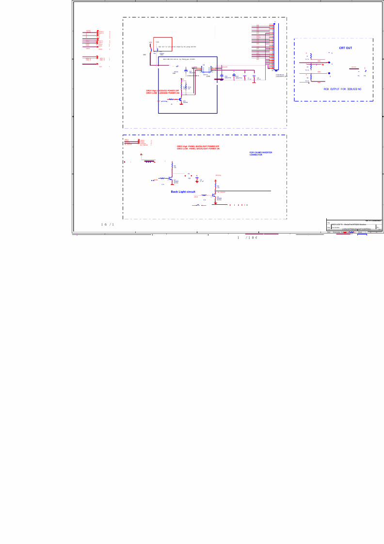
Opti nal f or 12V pannel. Added by bin_wang 16/ 7/05
Back Light circuit
FOR CHI-MEI INVERTERCONNECTOR
Add LVDS VCC cont rol by Zheng_guo 15/ 9/05.
ORO1 High :LVDSVDD POWER OFFORO1 LOW :LVDSVDD POWER ON
ORO3 High :PANEL BACKLIGHT POWER OFFORO3 LOW :PANEL BACKLIGHT POWER ON
AP[0..7]
AN[0..7]
RGB
VSYNCHSYNC
CLK1+CLK1-
CLK2-CLK2+
AN0 AP0 AN1 AP1
CLK1-
AN2 AP2
AN4
CLK1+
AP4
AN3
AN5 AP5
AP3
CLK2-CLK2+
AN6
AN7
AP7
AP6
+12V
BL_ON/OFF
PWM0
BL_ON/OFF
ORO3
Dimming
ORO3PWM0Dimming
ORO1
ORO1
LVDSVDD
AP[0..7] 3
AN[0..7] 3
+12V 1
CLK1+ 3CLK1- 3
CLK2+ 3CLK2- 3
G 3R 3
B 3
VSYNC 3HSYNC 3
Dimming 6BL_ON/OFF 6
ORO3 3PWM0 3
ORO1 3
VCC +12V
VCC
VCC
+12V
R211
2k
R4 0
+ CE1330uF/25v
C330UF25V/D8H14
C30.1uF
C10.1uF
Q9
IR7314SOP8
1234 5
678S1
G1S2G2 D2
D2D1D1
Q22N3904SOT23
1
2
3
+CE3220uF/16v
R9
4.7k
R7
4.7k
F1
4A/32v1206
R21022k
R20922k
R6
100k
+ CE2220uF/16v
J1
FI-SE30P-HFLVDS/30P/P1.25/S
123456789
10111213141516171819202122
2324252627282930
C20.1uF
R810k
FB2
75R/NC0805
FB1
75R0805
R510k
Q102N3904
1
2
3
Q12N3904SOT23
1
2
3
8/18/2019 Akai Lcd Tv Lct3201td_service Masnual
http://slidepdf.com/reader/full/akai-lcd-tv-lct3201tdservice-masnual 19/108
A
A
B
B
C
C
D
D
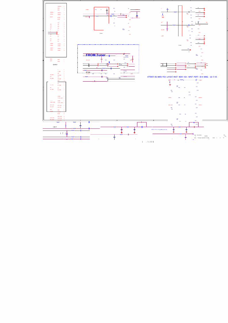
FROM Tuner
OUTPUT
I NPUT
AF Path
MODIFI ED BY BI N_WANG 16/7/ 05.
ATTENTI ON: WHEN PCB LAYOUT, MUS
Change.
CVBS1+
CVBS1-
BLUE
RED
GREEN
CB-
CB+
CR+
Y-
Y+
CR-
RED+
BLUE+
GREEN-
RED-
GREEN+
BLUE-
SY-
SY+
SC-
SC+
CVBS0+
CVBS0-
CVBS1+
CVBS1-
CVBS0
AF1_OUT
SIF1_OUT
MPX1
MPX2
VGASOG
GRN_GND
BLU_GND
RED_GND
Y
CR
CB
SOY
SC
SY
Y
CB_GND
CVBS0_GND
CVBS1
CVBS1_GND
Y_GND
Y_GND
CB_GND
CR_GND
SY
SY_GND
SC
SC_GND
AF1_OUT MPX2
MPX1
CVBS1
SY_GND
CVBS0_GND
CVBS0+CVBS0
CVBS0-
RED_GND
BLUE
GREEN
CR_GND
SC_GND
RED
CVBS1_GND
CB
CR
SIF1_OUT
GRN_GND
BLU_GND
RED 6
GREEN 6
BLUE 6
CB+ 3
CB- 3
CR+ 3
CR- 3
Y- 3
Y+ 3
BLUE+ 3
GREEN- 3
RED+ 3
RED- 3
GREEN+ 3
BLUE- 3
SY- 3
SY+ 3
SC- 3
SC+ 3
CVBS0+ 3
CVBS0- 3
CVBS1+ 3
CVBS1- 3
CVBS0 7
AF1_OUT 7
S IF 1_ OU T 7
MPX2 3
MPX1 3
VGASOG 3
B LU _G ND 6
G RN _G ND 6
R ED _G ND 6
CR 7
CB 7
Y 7
SOY 3,7
CVBS0_GND 7
CVBS1 7
CVBS1_GND 7
Y_GND 7
CB_GND 7
CR_GND 7
SY 7
SY_GND 7
SC_GND 7
SC 7
FB4
70R
R35 8.2K
C3015pF
C9
47nF
C2915pF
C2315pF/NC
R15
56R17
0
C2415pF/NC
+
CE5
47uF/16v
C5
47nF
C26
47nF/NC
FB8
70R
C11
47nF
C13330pF
R40 39k
R12 18
+
CE4
47uF/16v /NC
C15
47nF
FB6
70R
C7330pF
R21
22
C22
47nF
R41 39k
R13
22
8/18/2019 Akai Lcd Tv Lct3201td_service Masnual
http://slidepdf.com/reader/full/akai-lcd-tv-lct3201tdservice-masnual 20/108
A
A
B
B
C
C
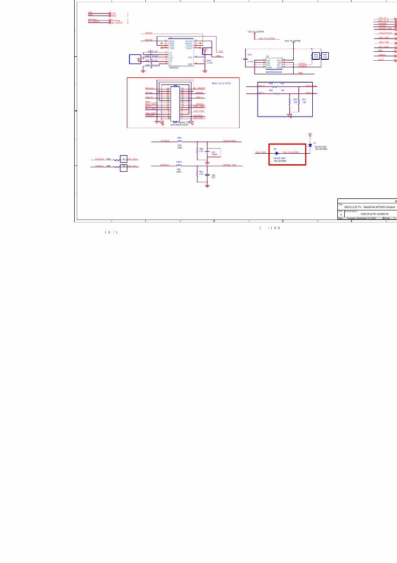
Modi f i ed by MI CO.
VGASDA
VGA_PLUGPWR
VGA_PLUGPWRVGA_PWR
VGASDA
VGASCL
VGA_SDA
VGA_SCL
VGA_R
VGA_L VG
VG
VGASCL
VGAVSYNC#VSYNC#
HSYNC# HSYNC_VGA
GND
RED
BLU_GNDVGA_PWR
VGA_SDAHSYNC#VSYNC#VGA_SCL
VGA_R
RSTXD
RSRXD
TXD
RXD
TXDRXD
Dimming BL_ON/OFF
RED_GNDBLUE
RSTXD
GREENGRN_GND
VGA_L
RSRXD
BL_ON/OFFDimming
TXD 3RXD 3
Dimming 9BL_ON/OFF 9
VGA_PLUGPWR
VGA_PLUGPWR
+5V
+5V
C47100pF
R54 15K
R55 15K
R56
75K
C485pF
R57
75K
FB9
70R0603
U1
MAX232A
138
1110
1345
26
129147
16
15
R1INR2INT1INT2IN
C+C1-C2+C2-
V+V-
R1OUTR2OUTT1OUTT2OUT
VCC
GND
D2
DIODE SMD
1N4148/SMD
J2
PC CONNECTORDIP14X2/P2.54/R1
2468
1012141618202224
135791113151719212325262728
FB10
70R0603
C41 0.1uF
C450.1uF
C43
0.1uF
R582.2k
C44 0.1uF
C42 0.1uF
R60 33
C46 0.1uF
R612.2k
R59 33
U2
EEPROM 24C02
1
234 5
67
8NCNCNCGND SDA
SCLWP
VCC
8/18/2019 Akai Lcd Tv Lct3201td_service Masnual
http://slidepdf.com/reader/full/akai-lcd-tv-lct3201tdservice-masnual 21/108
8/18/2019 Akai Lcd Tv Lct3201td_service Masnual
http://slidepdf.com/reader/full/akai-lcd-tv-lct3201tdservice-masnual 22/108
8/18/2019 Akai Lcd Tv Lct3201td_service Masnual
http://slidepdf.com/reader/full/akai-lcd-tv-lct3201tdservice-masnual 23/108
8/18/2019 Akai Lcd Tv Lct3201td_service Masnual
http://slidepdf.com/reader/full/akai-lcd-tv-lct3201tdservice-masnual 24/108
A
A
B
B
C
C
D
D
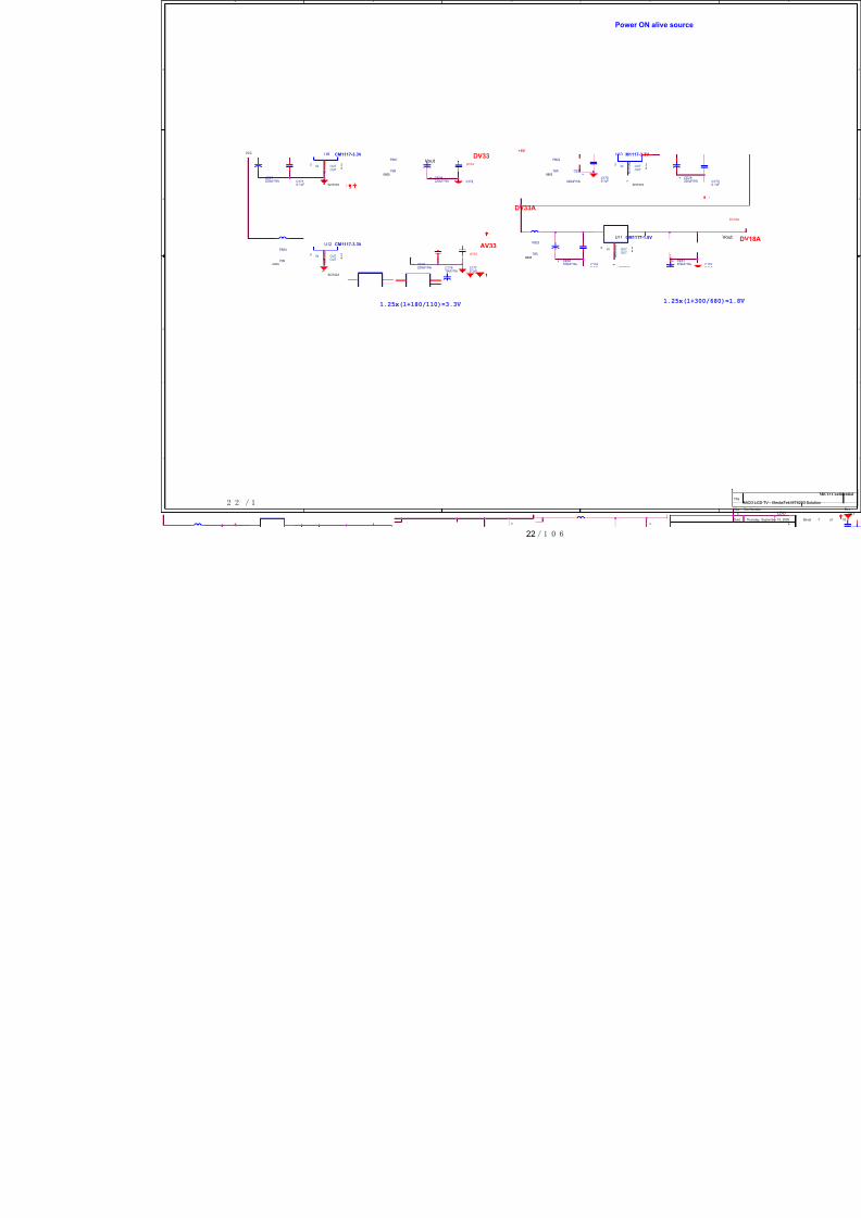
Vout
1.25x(1+180/110)=3.3V
Power ON alive
1
AV33
DV33
AV33
DV33
DV33A
VCC+5V
C1720.1uF
+ CE32
220uF/16v
U9 CM1117-3.3V
SOT223 1
234
A D J / G N D
OUTINOUT
U12 CM1117-3.3V
SOT223 1
234
A D J / G N D
OUTINOUT
C1770.1uF
+CE26
220uF/16vC1700.1uF
C17610uF/10v
+ CE28220uF/16v
+ CE27220uF/16v
U11 CM1117-1.8V
SOT223
1
234
A D J / G N D
OUTINOUT
FB23
75R0805
C174
0.1uF
C1710.1uF
FB24
75R0805
+ CE30100uF/16v
FB21
75R0805
FB22
75R0805
U10 M1117-3.3V
SOT223 1
234
A D J / G N D
OUTINOUT
22
8/18/2019 Akai Lcd Tv Lct3201td_service Masnual
http://slidepdf.com/reader/full/akai-lcd-tv-lct3201tdservice-masnual 25/108
A
A
B
B
C
C
D
D
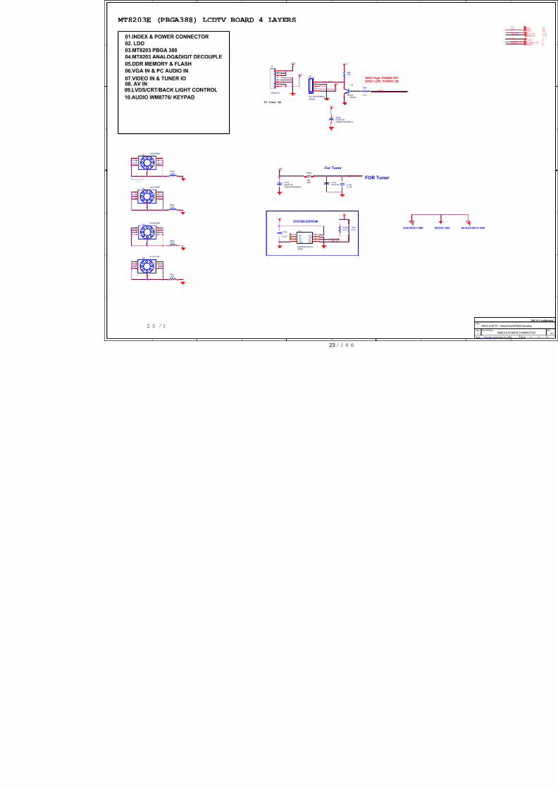
03.MT8203 PBGA 388
01.INDEX & POWER CONNECTOR
04.MT8203 ANALOG&DIGIT DECOUPLE
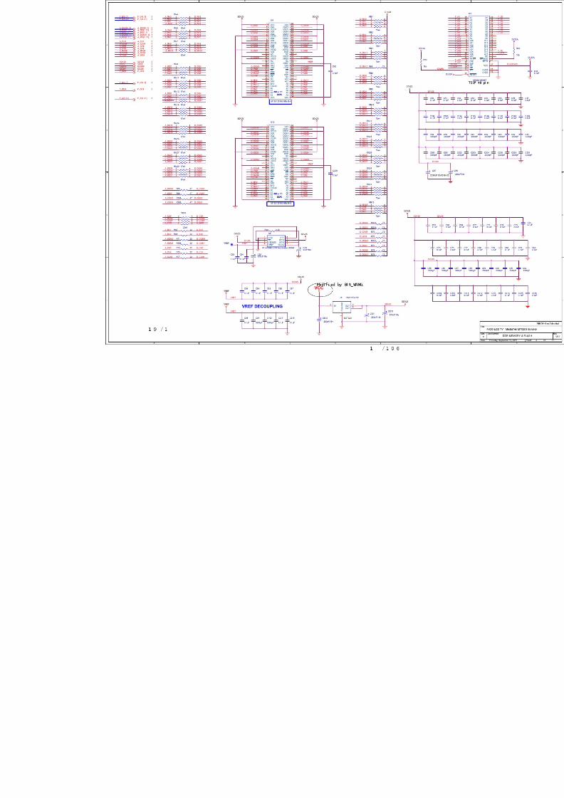
MT8203E (PBGA388) LCDTV BOARD 4 LAYERS
05.DDR MEMORY & FLASH
06.VGA IN & PC AUDIO IN
09.LVDS/CRT/BACK LIGHT CONTROL
10.AUDIO WM8776/ KEYPAD
02. LDO
07.VIDEO IN & TUNER IO08. AV IN
For Tuner
FOR Tuner
SYSTEM EEPROM
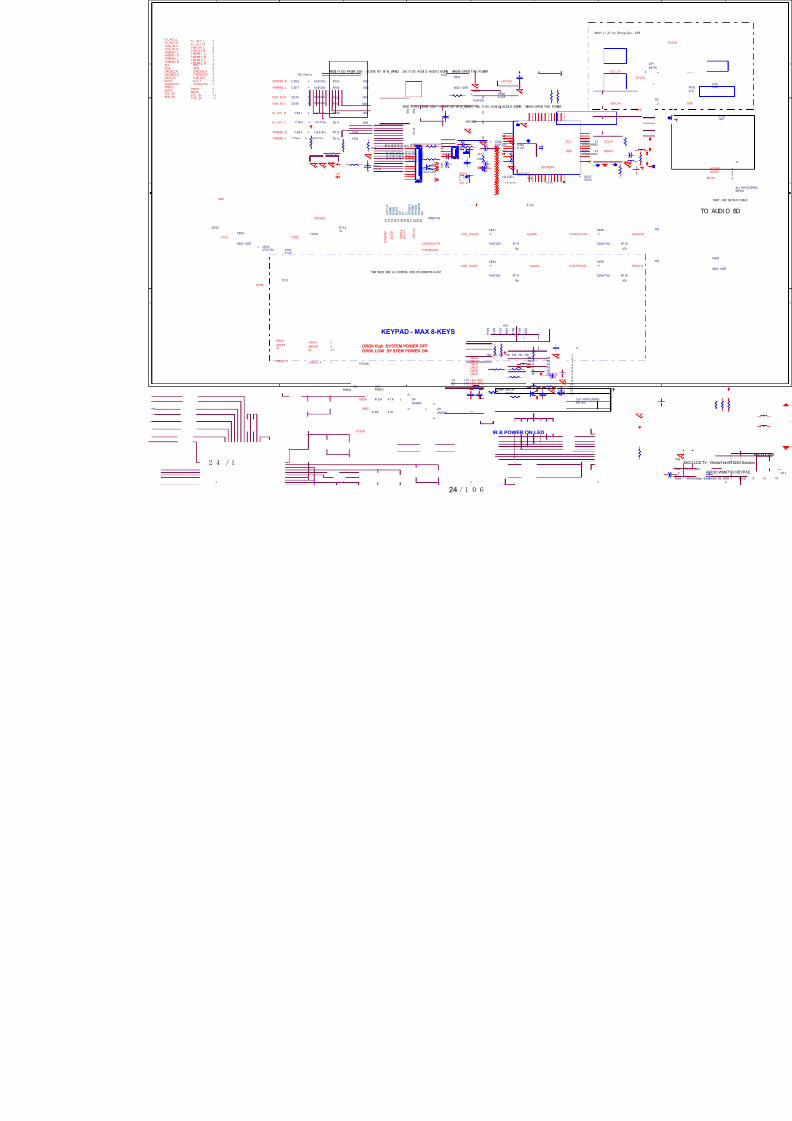
ORO7 High :POWER OFFORO7 LOW :POWER ON
TO Power BD
AUIO IN/OUT GND
SCL_5VSDA_5V
TUNER_12V
SYS_PWR
ORO7
+5V
+5V
+12V
+5V
+5VVCC
+12V
+5V
H2 HOLE/GND
2345
9876
1
2345
9876
1
H1 HOLE/GND
2345
9876
1
2345
9876
1
FB26
75R0805
+ CE33220uF/16vC220UF16V/D6H11
FB30120R
R1014.7k
C1780.1uF
H3 HOLE/GND
2345
9876
1
2345
9876
1
J4
5x1 W/HOUSING
SIP5\2
123
45
Q3
2N3904SOT23
1
2
3
FB31120R
+ CE3547uF/16v
R9810k
C179
0.1uF
R99
4.7k
+ CE34220uF/16vC220UF16V/D6H11
J3
DIP8/P2.0
1234567
8
H4 HOLE/GND
2345
9876
1
2345
9876
1
R1004.7k
U13
EEPROM 24C16SOP8
1234 5
678NC
NCNCGND SDA
SCLWP
VCC
FB27120R
FB25
120R
23
8/18/2019 Akai Lcd Tv Lct3201td_service Masnual
http://slidepdf.com/reader/full/akai-lcd-tv-lct3201tdservice-masnual 26/108
A
A
B
B
C
C
D
D
TWO WI RE SERI AL CONTROL DEVI CE ADDRESS 0x34h
Del Part sMODI FI ED FROM 10K- - >100K BY BI N_WANG . 16/ 7/ 05. AVOI D AUDI O BOMB WHEN OPEN THE POWER
MODI FI ED FROM 10K-- >100K BY BI N_WANG . 16/ 7/ 05. AVOI D AUDI O BOMB WHEN OPEN THE POWER
POWER ON/ OFF
KEYPAD - MAX 8-KEYS
IR & POWER ON LED
Modif y I 2C b
ORO0 High :SYSTEM POWER OFFORO0 LOW :SYSTEM POWER ON
GA_IN_LGA_IN_R
UTE
PBPR1_LPBPR1_R
WM1
_AV1_R
OSDATA1OUT
PWM1
ACLRCACMCLK
_AV1_L
ACBCLKDACL
PBPR2_LPBPR2_R
DOUT
CODHPOUTL
AUXL
COD_VOUTL
H P V D D
VMIDDACDACBCLK
S C L 1 4
CODHPOUTR
COD_VOUTR
S1_AV1_L
VGA_IN_L
HPVDD
ADCREFP
YPBPR2_L
DACMCLK
VMIDADC
AUSPL
AUXR
DACLRC
HPVDD
DACMCLK
YPBPR1_L
VMIDADCDACBCLK
DVDD
S1_AV1_R
D A C L R C
AOSDATA1
YPBPR2_R
YPBPR1_R
AUSPR
D V D D
VGA_IN_R
HPVDD_A
S D A 1 4
DACLRC
DV33COD_VOUTR
GND
COD_VOUTL
ADCREFP
CODHPOUTL
CODHPOUTR
OBO7
CH-
VOL+VOL-MENUTV/AV
OBO6
LED_REDLED_GRN
DV33A
URST#
ORO0
IR
OBO[0..7]
SC
SD
OBO1
ORO0
OBO5OBO4
OBO3OBO2
OBO0
CH+IR
SCL
SDA
SCL14
SDA14
CL_5VDA_5V
V GA _I N_ L 6V GA _I N_ R 6
MUTE 3
Y PB PR 1_ L 7Y PB PR 1_ R 7
S 1_ AV 1_ R 7
AOSDATA1 3
PWM1 3
DOUT 3
S 1_ AV 1_ L 7
DACMCLK 3D AC LR C 3
DACBCLK 3
SCL 3SDA 3
Y PB PR 2_ R 7Y PB PR 2_ L 7
URST# 3
ORO0 3
IR 3,7
O BO [0 .. 7] 3
S CL_ 5V 1,7S DA_ 5V 1,7
VCC
DVDD
HPVDD
DV33
DV33A
+5V
DV33A
+5V
R 1 9 7
10k
TP10
R1141k
R 12 4 4 .7 K
+CE39 10uF/25v
+C E3 6 10 uF/25v
R108 100k
R193
33R
R 20 8 3 3R/SMD/0603
FB35 FB
C1860.1uF
R12010K
R0603
R117
10k
+
CE55
220uF/16v
Q4
2N39061
2
3
R 1 9 6
10k
R113 100k
+C E4 8 1 0u F/ 25 v
+CE40 10uF/25v
+ CE4910uF/25v
R102 100k
C1800.1uF
+ CE4710uF/25v
FB39 FB
R 1 9 5
10k
R111 100k
FB34 FB
Q5
2N39061
2
3
R104 100k
R106 100k
J6
13x1 W/HOUSINGSIP13\2
12345
6789
10111213
+C E3 7 10 uF/25v
R 1 9 4
10k
R 2 0 0
10k
R 1 1 0
5 0 k
C1840.1uF
FB33
0603 120R
+C E4 3 1 0u F/ 25 v
+ CE5347uF/16v
+
CE51
10uF/25V
+ CE4510uF/25v
TP6
FB32
0603 120R
FB38 FB
R126 0
C1850.1uF
+C E4 1 1 0u F/ 25 v
U14
WM8776
123456789
101112
1 3
1 4
1 5
1 6
1 7
1 8
1 9
2 0
2 1
2 2
2 3
2 4
252627282930313233343536
3 7
3 8
3 9
4 0
4 1
4 2
4 3
4 4
4 5
4 6
4 7
4 8
AIN2L AIN1R AIN1LDACBCLKDACMCLKDINDACLRCZFLAGRZFLAGL ADCBCLK ADCMCLKDOUT
A D C L R C
D G N D
D V D D
M O D E
C E
D I
C L
H P O U T L
H P G N D
H P V D D
H P O U T R
N C
NCVOUTLVOUTR
VMIDDACDACREFNDACREFP
AUXR AUXL
VMIDADC ADCREFGND
ADCREFP AVDD
A G N D
A I N V G R
A I N O P R
A I N V G L
A I N O P L
A I N 5 R
A I N 5 L
A I N 4 R
A I N 4 L
A I N 3 R
A I N 3 L
A I N 2 R
+C E4 4 1 0u F/ 25 v
R 1 0 9
5 0 k
R107 100k
C1830.1uF
+
CE54
10uF/25v
R112 100k
R1 23 N C/ 0
FB37 FB
R 125 4.7K
R119 510
C1870.1uF
R 1 9 9
10k
R12110KR0603
+
C E4 2 1 0u F/ 25 v
FB36 FB
R122 510
R 1 9 8
10k
R 20 7 3 3R/SMD/0603
+CE38
10uF/25v
+ CE5010uF/25v
+
CE52
220uF/16vR115
10k
+C E4 6 1 0u F/ 25 v
TP7
24
8/18/2019 Akai Lcd Tv Lct3201td_service Masnual
http://slidepdf.com/reader/full/akai-lcd-tv-lct3201tdservice-masnual 27/108
A
A
B
B
C
C
D
D
NEARLY YPBPR2-CON.
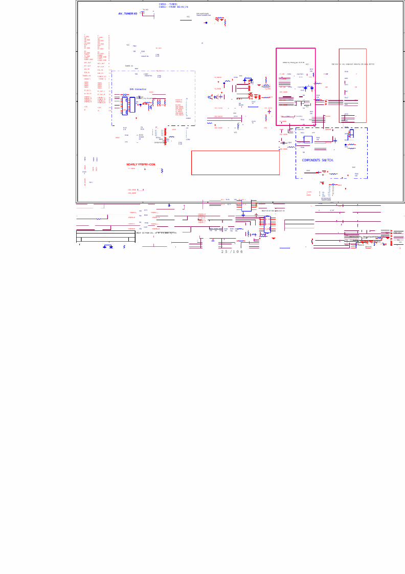
CVBS0-- - TUNER1CVBS1-- - FRONT BD AV_I N
AV , TUNER I/O
NEARLY YPBPR1-CON.
MODI FI ED BY BIN_WANG. 16/7/ 05
COMPONE
MODIFI ED FROM 15k-- >0 BY BI N_WANG 16/7/ 05.
Added by Zheng_guo 21/7/ 05
DVD Connector
8/18 modif y by st evenPBPR1_LPBPR1_R
Y2_GNDB
CB2_GNDB
CR2_GNDB
TU_VCC
CB1SWB
CB
GNDSYY2SWBY1SWB
CB2SWB
PBPR2_LPBPR2_R
YPBPR1_L
TU_12V
_
O G O 0
O G O 1
C_GND
V_GND
B_GND
C
VBS0
_GND
VBS1
OYR_GND
Y
R
VBS1_GND
B
DA_5V
CL_5V
Y_GND
YPBPR1_L
YPBPR1_R
YPBPR2_L
YPBPR2_R
YPBPR1/L
YPBPR1/R
YPBPR2/L
YPBPR2/R
YPBPR2_LYPBPR2_R
SDA_5VSCL_5V
Y
AF1_OUTSIF1_OUT
TV_GND
ER_12V
Y1_GNDB
_AV1_L
_AV1_R
GO[0..1]
RO6RO4
CVBS0
RO2
ORO2
Y1_INB
CB1_INB
CR1_INB
CR2B
Y2B
CB2B
AV_L S1_AV1_L
S1_AV1_LS1_AV1_R
F1_OUT
F1_OUT
Y_GND
CR1_GNDB
AV_R S1_AV1_R
Y2B
CB2B
CR2B
IR_DVD
CR2_INDVDCR2_GNDB
CB2_INDVD
Y2_INDVDY2_GNDB
CR2_INDVD
CB2_INDVD
Y2_GNDB
Y2_INDVD
Y2_GNDB
YPBPR2/LYPBPR2/R
YPBPR1_R
CB_GND
CB1_GNDB
Y1_INBY1_GNDB CB1_GNDB
CVBS1
SC_GND
Y1_GNDB
CB1_GNDB
CR1_GNDB
Y2_GNDB
CB2_GNDB
CR2_GNDB
CB2_GNDB CB2_GNDBCB2_GNDB
CR2_GNDBCR2_GNDB
ORO5
VDVD
CB1_INB
CR1_INBCR1_GNDB
SC
SY SY_GND
AV_R AV_L
YPBPR1/RYPBPR1/L
RO5
2VIR_DVD
IR
ORO4
CVBS1_GND
CR_GND
Y PB PR 1_ L 1 0YPBPR1_R 10
CB 8
SC 8
CVBS0_GND 8CVBS0 8
SOY 3
SC_GND 8
CR_GND 8
SY 8
CVBS1_GND 8
Y 8
CVBS1 8
CR 8CB_GND 8
Y_GND 8
S DA _5 V 1 ,1 0
S CL_ 5V 1,1 0
TUNER_12V 1
YPBPR2_R 10Y PB PR 2_ L 1 0
S 1_ AV 1_ L 1 0
S 1_ AV 1_ R 1 0
OGO[0..1 ] 3
ORO6 3ORO4 3
ORO2 3
S IF 1_ OU T 8
AF1_OUT 8
SY_GND 8
ORO5 3
+12V 1,9
IR 3,10
TUNER_12V
VCC
DV33
VCC
VCC
VCC
TU_VCC
TU_12V
VCCVCC
VCC
VCC
VCC VCC
VC
VC
VCC
VCC
VCCVCC
VCC
R148
10K
R16775
R18175K
R185
75K
R162
4.7k
+C E6 2 2 2u F/ 10 V
FB41
70R
J7
CON12SIP12\2
123456789101112
Q7
IR7314SOP8
1234 5
678S1
G1S2G2 D2
D2D1D1
J9
CON10
12345678910
R14610k
R17075
R139
10K
R18475K
R18715K
R137
10K
R18275K
R15610k
+C E6 4 2 2u F/ 10 V
R177 15K
C1900.1uF
C1890.1uF
R166
10K
R158 0
O G O 0
D9BAV99
1 2
3
R161
10K
R18375K
Q6
2N3904
SOT23
1
2
3
R
1
O G O 1
R165 0
D7BAV99
1 2
3
C1880.1uF
+C E5 8 2 2u F/ 10 V
+CE63
470uF/16vC470UF16V/D8H14
R17110K
R17915K
TP11
R176 15K
D8BAV99
1 2
3
J9
VIDEO CONNECTORDIP11X2/P2.54/R2
2468
101214161820
1357911131517192122
R151
10K
FB43
70R
R154
10K
+C E5 9 2 2u F/ 10 V
R
1
R18015K
9
R14910k
R168 0
+CE56
1000uF/16v
+C E6 0 2 2u F/ 10 V
J10
CON5
12345
Q8
2N3904
SOT23
1
2
3
R1574.7k
R18815K
R16075
+C E6 1 2 2u F/ 10 V
R186
75K
R143
10K
+CE571000uF/16v

8/18/2019 Akai Lcd Tv Lct3201td_service Masnual
http://slidepdf.com/reader/full/akai-lcd-tv-lct3201tdservice-masnual 28/108
1 2 3 4
4321
MUTEC
MUTEC
USPL
+24V
PR
PIN1
NIN2
AGND3
EN4
BS
VPP
SW
PGND
U3
ATA-120
1 2R15 47K
5%
PIN1
NIN2
AGND3
EN4
BS
VPP
SW
PGND
U1
ATA-120
C20
10UF
1 2
C30
4.7nF
NPO
1
2
R36
10K
5 %
1 2
R16
100K 5%
12
R18
10K
5 %
12
R1
82K
5%
12
C1
22pF NPO
C34
NS
1 2
R2
100K 5%
1
2
C5
4.7uF
X5R
C24
22pF
C12
100NF
1 2
C31
1UF
X5R
1
2
C27
4.7uF
X5R
1 2
C3
1UF
X5R
12
R7
10K
5%
1
2
R37
10K
5 %
1 2R12
10K 5%
+
1
2
C10
100UF/25V
1
2
R17
100K
5 %
C41
22pF
1
2
R4
100K5%
12
C21
22p F NPO
+5
-6
OUT 7
U2B
RC4558
12
R3
10K
5%
1 2
C8
4.7nF
NPO
1
2
R11
10K
5 %
C14
22UF/16V
C19
22UF/16V
+3
-2
OUT 1
U2A
RC4558
C40
10UF
1
2
R10
10K
5 %
12
R14
82K
5%
1
2
R5
100K
5 %
1 2R39
10K 5%
C15
2.2UF
1
2
R19
100K
5%
12
R21
10K
5%
1 2R38
47K
5%
AGND
AGND
+24V
A
12 R66
4K75%
12 R67
4K75%
C541n
C551n
C521n
C531n
12 R46
4K75%
12 R45
4K75%
12 R47
1K85%
12 R33
1K85%
8/18/2019 Akai Lcd Tv Lct3201td_service Masnual
http://slidepdf.com/reader/full/akai-lcd-tv-lct3201tdservice-masnual 29/108
1 2 3 4
4321
+24V
A
MUTE
R30
22k
D5
NC
D6
1N4148
D8
1N4148
D9
1N4148
R43
0R
AUSPL
AUSPR 1 2
R57 4K7
5%
1 2R63 10K
5%
1 2
R 48 1 k8
5%
C2
100U/35V
1 2
R58 4K7
5%
+5
-6
OUT 7
U5B
RC4558
1 2
R52 22K
5%
1 2
R64 22K
5%
1 2
R49 4K7
5%
1 2
R59 10K
5%
1
2
C45
1n 1
2
R65
47K
5%
1 2
R50 4K7
5%
1 2
R54 10K
5%
1
2
C46
1n
1
2
R60
100K
5 %
+3
-2
OUT 1
U5A
RC4558
1
2
C47
1n
C43
10U/16V
1 2
R51 10K
5%
1 2
R55 10K
5%
1
2
R61
47K
5%
1
2
C48
1n
C44
22U/16V
1 2C49
22P
C22
22U/16V
1 2
R56 1k8
5%
1
2
R53
100K
5 %
1
2
C13
100N
1 2C50
22P
1 2R62 10K
5%
C26
10U/16V
+24V
+24V
AGND
AGND
AGND
AGND
12 C60
10UF
X5R
12 C59
10UF
X5R
12 R13
1K 5%
12 R26
1K 5%
LOUT
ROUT
27
8/18/2019 Akai Lcd Tv Lct3201td_service Masnual
http://slidepdf.com/reader/full/akai-lcd-tv-lct3201tdservice-masnual 30/108
8/18/2019 Akai Lcd Tv Lct3201td_service Masnual
http://slidepdf.com/reader/full/akai-lcd-tv-lct3201tdservice-masnual 31/108
8/18/2019 Akai Lcd Tv Lct3201td_service Masnual
http://slidepdf.com/reader/full/akai-lcd-tv-lct3201tdservice-masnual 32/108
Basic Operations & Circuit Description
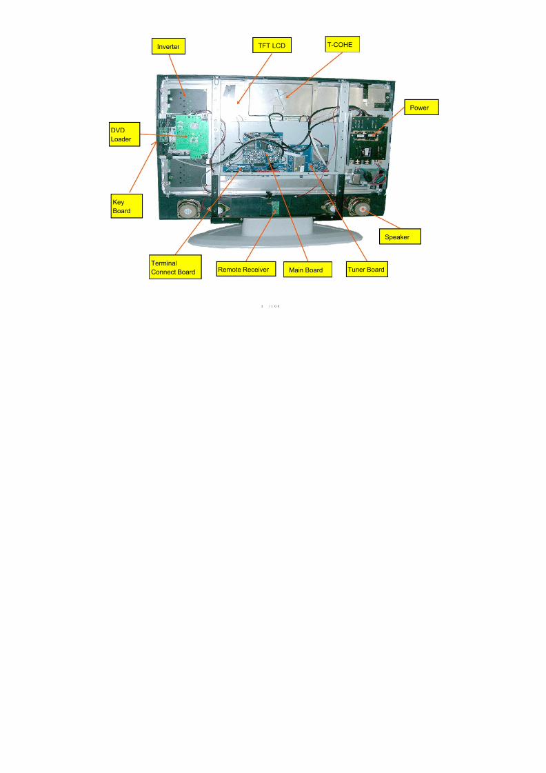
Main Electric Components(1). MODULE:
There are 1 pc. panel and 2 pcs. PCB including 1 pc. INVERTERboard(L), 1 pc. T-CONTROL board,
(2).SIGNAL PROCESSThere are 5 pcs. PCBs including
1 pc. Audio&Tuner board,1 pc. Main digital board,1 pc. Keypad board,1 pc. Remote Control Receiver board,1 pc. DVD decoder board
(3).POWERThere are 1 pc. PCB for power.
8/18/2019 Akai Lcd Tv Lct3201td_service Masnual
http://slidepdf.com/reader/full/akai-lcd-tv-lct3201tdservice-masnual 33/108
PCB function1. Power:(1). Input voltage: AC 100V~240V, 47Hz~63Hz.Input range: AC 90V(Min)~264V(Max) auto regulation.(2). To provide power for PCBs.
a). +24V for Inverter.b). +5Vsb for standby,c). +5V for signal power,d). +24V for Audio Amp power and converter to
e). +12V for Tuner power.
2. Main (Video InterFace) board:(1).Decoder the video signal (TV,CVBS,S-VIDEO) from analog to digitalsignal.
(2).Converter the Video signals( TV,CVBS,S-VIDEO ) and graphics signal(VGA,YPbPr) from inter f ace to progressive,(3). Converter the Digital to fit the panel display mode and output the LVDSsignal to Panel.
3. Tuner & Audio Board:(1)Convert TV RF signal to video and audio signal to Main board.(2 ). Decoder the TV SIF signal to audio signal,(3 ). Converter the audio to audio Amp lifier and output to the speaker.
4. KEYBOARDTo get the main button control on LCD_TV as SOURCE,MENU,CHANEL +,CHANEL -, VOL +,VOL-, STANDBY functions.
5. Remote control boardReceive the remote signal and active for the control.
6. T-CONTROL board
Converter the LVDS signal to the digital signal for fitting the PANEL.
7. INVERTER board
Converter the low DC voltage +24V to high AC voltage to drive the backlight.
8/18/2019 Akai Lcd Tv Lct3201td_service Masnual
http://slidepdf.com/reader/full/akai-lcd-tv-lct3201tdservice-masnual 34/108
PCB failure analysis1. CONTROL:
a. Abnormal noise on screen.b. No picture.
2. MAIN (VIDEO):a. Lacking color, Bad color scale.b. No voice.c. No picture but with signals output, OSD and back light.d. Abnormal noise on screen.
3. POWER:No picture, no power output.
Basic operation of LCD-TV1. After turning on power switch, power board sends 5Vst-by Volt to Micro
Processor IC waiting for ON signals from Key Switch or Remote Receiver.
2. When the ON signal from Key Switch or Remote Receiver is detected, MicroProcessor will send ON Control signals to Power. Then Power sends (5Vsc,12Vsc, 24V and RLY ON, Vs ON) to PCBs working. This time VIF will sendsignals to display back light, OSD on the panel and start to search available
signal sources. If the audio signals input, them will be amplified by Audio AMPand transmitted to Speakers.
3. If some abnormal signals are detected (for example: over volts, over current,over temperature and under volts), the system will be shut down by Power off.
8/18/2019 Akai Lcd Tv Lct3201td_service Masnual
http://slidepdf.com/reader/full/akai-lcd-tv-lct3201tdservice-masnual 35/108
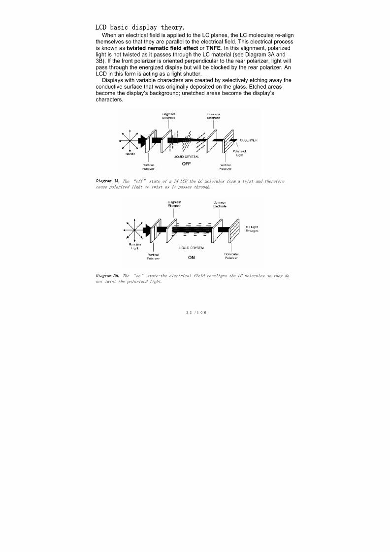
LCD basic display theory
When an electrical field is applied to the LC planes, the LC molecules re-alignthemselves so that they are parallel to the electrical field. This electrical processis known as twisted nematic field effect or TNFE. In this alignment, polarizedlight is not twisted as it passes through the LC material (see Diagram 3A and
3B). If the front polarizer is oriented perpendicular to the rear polarizer, light willpass through the energized display but will be blocked by the rear polarizer. AnLCD in this form is acting as a light shutter.
Displays with variable characters are created by selectively etching away theconductive surface that was originally deposited on the glass. Etched areasbecome the display’s background; unetched areas become the display’scharacters.
Diagram 3A The “off” state of a TN LCD-the LC molecules form a twist and thereforecause polarized light to twist as it passes through.
Diagram 3B The “on” state-the electrical field re-aligns the LC molecules so they do
not twist the polarized light.
8/18/2019 Akai Lcd Tv Lct3201td_service Masnual
http://slidepdf.com/reader/full/akai-lcd-tv-lct3201tdservice-masnual 36/108
TFT LCD T-COHE
Pow
Speaker
Tuner Board Main BoardTerminal
Connect Board
VD
oader
Key
Board
Remote Receiver
Inverter
8/18/2019 Akai Lcd Tv Lct3201td_service Masnual
http://slidepdf.com/reader/full/akai-lcd-tv-lct3201tdservice-masnual 37/108
IC DESCRIPTION
-MT8205G
-AT24C02
-MX29LV160BBTC
-LP2996
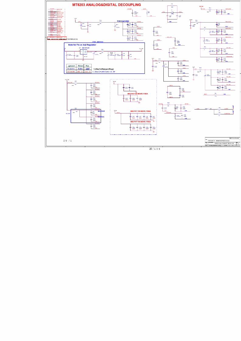
-AZ1117/H
-WM8776
-MX232A
-ISAV330
8/18/2019 Akai Lcd Tv Lct3201td_service Masnual
http://slidepdf.com/reader/full/akai-lcd-tv-lct3201tdservice-masnual 38/108
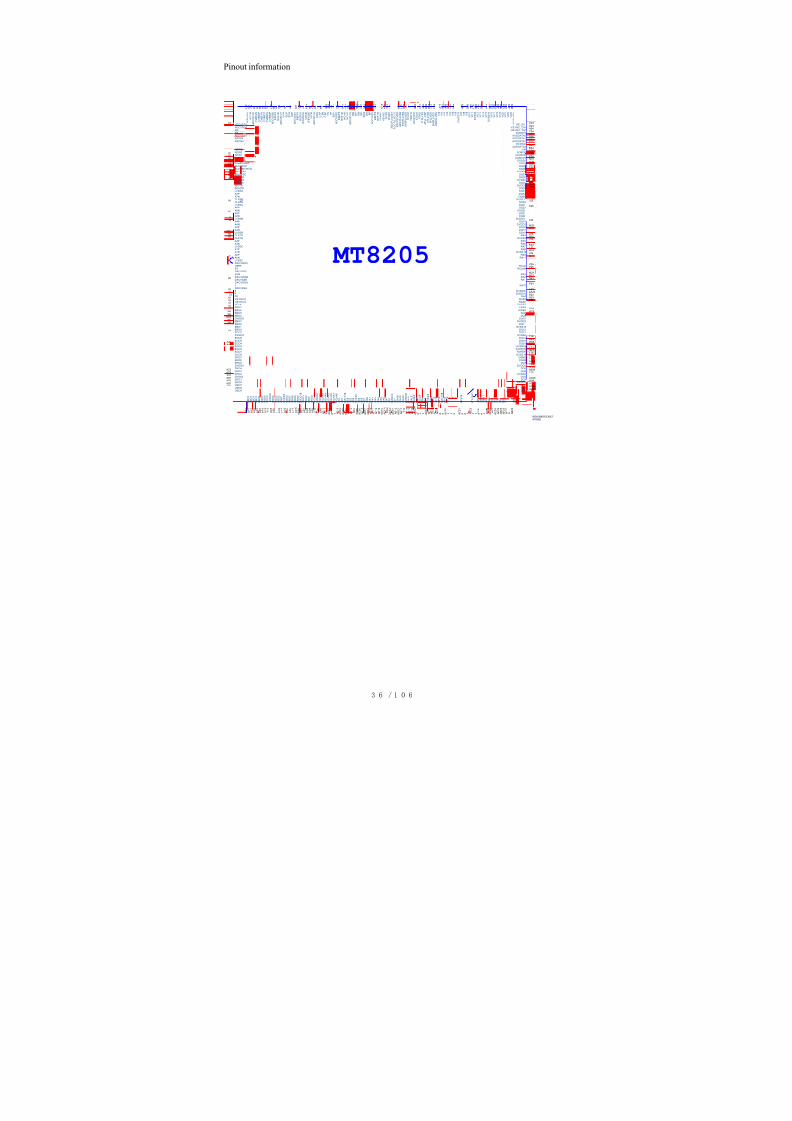
Pinout information
H I G H A 2
A C 1 1
DVSS18 T16
D V D D 1 8
A D 1 9
A3PM2
H I G H A 6
A E 9
V I 9
C 2 0
V
C L K_ D V I
B 2 3
DVSS3 N15
DLLVSSK3
B P
A 1 3
CKE N26
F C I C L K
A F 2 2
A D 5
A D 1 6
DQ30 D26
EBO4W2
A P L L V S S
D 1 8
A1NR1
DVDD2 H24
S C N
B 5
V I C M
A 7
ADCVSSF2
ERO4 AC2
DQ9 V25
V I 1 7
C 2 2
LVDDBL4
BGA388/SOCKET
A
D C V D D 3
D 8
A7NG1
DQ16 N25
RV4
AOSDATA2 B26
ADIN0E4
H I G H A 0
A F 1 2
VREFM4
S Y
S P L L V S S
L 1 5
BA1 P23
U P 1 5
A D 2 0
DVSS2 R15
DVSS3R11
C V B S 1 P
A 2
DQS3 H25
V I 3
A 1 8
U P 1 7
A F 2 1
D V D D 1 8
A D 1 8
Y N
B 1 0
S C L 1
A B 2 3
W R #
A F 1 8
DVDD2 H23
VPLLVDDG4
EGO1 AB1
V I 1 9
A 2 2
DVDD2 V23
A2NP1
R P
A 1 1
F C I D A T
A F 2 3
EGO2 AA4
AOSDATA3 B25
DACVDDCN3
A 1 7
A C 1 7
D V D D 3 I
A C 1 0
G P
A 1 2
X
T A L V D D
C 1 6
V I 5
C 1 9
A6NJ1
PWM2VREFF4
H I G H A 3
A F 1 0
C V B S 0 P
A 3
I O A 1 9
A D 1 2
V I 1 3
C 2 1
S O Y
C 8
DQS0 Y25
O G O 6
A F 4
DQ4 AB25
U P 3 4
A D 2 2
RA6 K23
I O A 3
A F 1 4
A5NK1
D V D D
D 1 4
DQ12 U26
ADCVDDF1
O G O 2
A F 5
D V S S 1 8
T 1 1
A V C M
D 5
DVSS18 P14
U P 3 0
A E 2 1
D M
P L L V D D
C 1 7
ADIN4D4
HSYNCOU2
V
F E V D D 0
D 7
D V S S 3
R 1 3
AVDD18 Y23
V I 1 5
A 2 1
R E F N 2
C 9
I C E
A C 2 4
A D 6
A C 1 6
VCLKV1
CAS# T23
EBO0Y2
I O A 2 1
A F 1 1
A D C P L L V D D 1
D 1 5
DVSS2 N16
REFP4D1
C V B S 2 N
B 1
DQ21 K26
SIFC1
DQ17 M26
EBO1Y1
MT8205
V I 0
B 1 6
C V B S 1 N
B 2
V F E V S S 0
N 1 3
M O N 1
C 1 1
OBO7 AD3
I N T 0 #
A F 1 9
DQ2 AC25
RA9 L24
A D 7
A F 1 7
EBO6V3
VSYNC_DVI D24
BGVDDH4
R E F P 3
D 1 2
I O A 1 8
A E 1 2
RA0 R26
DVSS18P11
O R O 7
A E 6
DQ25 G25
ERO0 AD2
A 1 6
A E 8
I O A 7
A C 1 3
A0PT2
S Y N
B 6
DVDD18 AA24
ADCVDD4D3
V I 1 1
A 2 0
DQ15 R25
DQ3 AC26
DVDD18 AC18
C B P
A 9
VSYNCOU1
U P 3 1
A D 2 1
RA4 J23
DVDD18 Y24
SVMT4
EBO2W4
V S Y N C
C 1 3
A7PG2
DVSS2 P15
O G O 1
A C 6
LVDDCM3
DVDD2 F24
DQM1 H26
VPLLVSSJ3
H I G H A 1
A D 1 1
A
D C V S S 1
M 1 3
V I 1 2
B 2 0
G P I O 0
A E 2 3
T E S T N
A 1 4
O R O 4
A D 7
I O C S #
A C 1 4
O G O 4
A D 5
U?
V I 2 1
C 2 3
AVSS18 W23
I O A 2 0
A E 1 1
GU4
C R P
A 8
DET3
V F E V S S 1
L 1 2
AOBCK C26
S D A 0
A E 2 6
X T A L I
A 1 5
A1PR2
R E F P 0
B 4
DQ23 J26
D V D D 1 8
E 2 3
O R O 0
A D 8
DQ13 T25
D V S S 1 8
P 1 3
DQ6 AA25
P W M 1
A C 2 3
DVSS2 R16
ERO6 AB4
H I G H A 5
A F 9
V I 2 3
A 2 3
R D #
A E 1 8
REXTAJ4
B N
B 1 3
I O A 1
A D 1 4
DVSS18 T13
DACVDDAP4
AOMCLK E24
DVSS2 P16
A
P L L_ C A P
A 1 6
CLK1NN1
RVREF G23
A D 1
A D 1 5
A
D C V D D 1
C 5
O B O 3
A F 1
RA2 N23
O G O 5
A C 5
EBO3W3
V I 8
B 1 9
V I 1 6
B 2 1
ERO1 AD1
LVSSCN12
DQ7 AA26
BA0 R24
AFC2
A
D C V S S 3
C 1 0
AOSDATA1 A26
BGVSSK4
A D 0
A E 1 5
A D C P L L V S S
M 1 4
RA7 K24
O G O 7
A E 4
CLK1PN2
DQ31 D25
EBO5W1
V I 2
B 1 7
DVDD2 V24
A
D C V D D 2
C 7
S C L
A F 2 5
DVSS18 R14
ADIN2E2
EGO5 AA1
O G O 0
A D 6
I O A 4
A F 1 3
V I 1 8
D 2 2
LVSSBM11
DACVDDBP3
DVDD3I AC9
R N
B 1 1
U P 1 4
A E 2 0
RA10 P24
A D 4
A E 1 6
DVDD3I F23
S Y S P L L V D D
D 1 6
RCS# R23
A6PJ2
A2PP2
C V B S 0 N
B 3
DVDD2 G24
DQ1 AD26
ERO7 AB3
V I 4
B 1 8
V I 2 0
B 2 2
O R O 6
A F 6
EBO7V2
S C L 0
A F 2 6
Y P
A 1 0
DQ5
AB26
S D A 1
A B 2 4
U P 3 5
A C 2 2
DVDD18 AA23
I O A 0
A D 1 7
LIN B24
FSN4
LVSSAM12
G N
B 1 2
D V S S
N 1 4
S D A
A E 2 5
DLLVDDH3
EGO0 AB2
O B O 0
A F 3
DQ10 V26
DQ28 E26
RA5 J24
A4NL1
A
D C V S S 0
L 1 3
A P L L V D D
D 1 7
ADIN3E1
O R O 1
A C 8
O R O 3
A E 7
R E F N 1
C 6
DQM0 Y26
I O A 6
A D 1 3
V I 1 4
D 2 1
DVSS2 T14
I O A L E
A E 1 7
D V S S 3
R 1 2
R E F P 2
D 9
DQ0 AD25
P R S T #
A C 2 1
H I G H A 4
A E 1 0
O R O 2
A F 7
A D C
P L L V S S 1
L 1 4
T X D
A D 2 4
DVSS2 T15
REFN4D2
O G O 3
A E 5
O B O 1
A E 3
A
D C V D D 0
C 4
DQ29 E25
DACVSSAR4
DQ11 U25
D M
P L L V S S
C 1 8
ADCVSS4L11
V O C M
B 7
I O A 2
A E 1 4
D V D D 3
A D 1 0
R X D
A E 2 4
RA11 M23
D V S S 1 8
M 1 6
DE_DVI C24
M O N 0
D 1 1
A D C
P L L V D D
C 1 5
I O O E #
A F 1 5
T E S T P
B 1 4
EGO7Y3
O B O 4
A E 2
DQ24 G26
O B O 2
A F 2
EGO6Y4
BU3
A D 2
A C 1 5
DVDD2I U23
DQ8 W26
V I 1
A 1 7
LVDDAL3
C V B S 2 P
A 1
S C P
A 5
DQ20 L25
DQ18 M25
V I 1 0
D 2 0
RA8 L23
ADIN1E3
C B N
B 9
ERO2 AC4
U P 1 2
A E 1 9
DVDD2 W24
HSYNC_DVI A24
RA1 N24
DACVSSCN11
H I G H A 7
A F 8
RWE# U24
CLK2PH2
R E F N 3
C 1 2
U P 1 3
A F 2 0
RA3 M24
EGO4 AA2
D V D D 3
A D 9
ERO5 AC1
DQ26 F26
CLK2NH1
A0NT1
I O A 5
A E 1 3
S Y P
A 6
DQ27 F25
DQ19 L26
D V S S 1 8
P 1 2
F C I C M D
A E 2 2
AUXVTOPF3
D V S S 3
L 1 6
DQS1 W25
C R N
B 8
ERO3
AC3
D V S S 1 8
T 1 2
AOSDATA0 A25
RCLKB P25
DACVSSBR3
H S Y N C
C 1 4
X T A L O
B 1 5
A5PK2
MT8205
VFEVDD1C3
R E F P 1
D 6
DQS2 J25
RCLK P26
A D 3
A F 1 6
V I 6
D 1 9
EGO3 AA3
RAS# T24
A
D C V S S 2
D 1 0
U P 1 6
A C 2 0
P W M 0
A D 2 3
OBO5 AE1
V I 2 2
D 2 3
DQ14 T26
A4PL2
S O G
D 1 3
O R O 5
A C 7
AOLRCK C25
D V D D 1 8
A C 1 9
X T A L V S S
M 1 5
A3NM1
R E F N 0
A 4
DQ22 K25
AUXVBOTTOMG3
OBO6 AD4
V I 7
A 1 9
I O W R #
A C 1 2
I R
A F 2 4
8/18/2019 Akai Lcd Tv Lct3201td_service Masnual
http://slidepdf.com/reader/full/akai-lcd-tv-lct3201tdservice-masnual 39/108
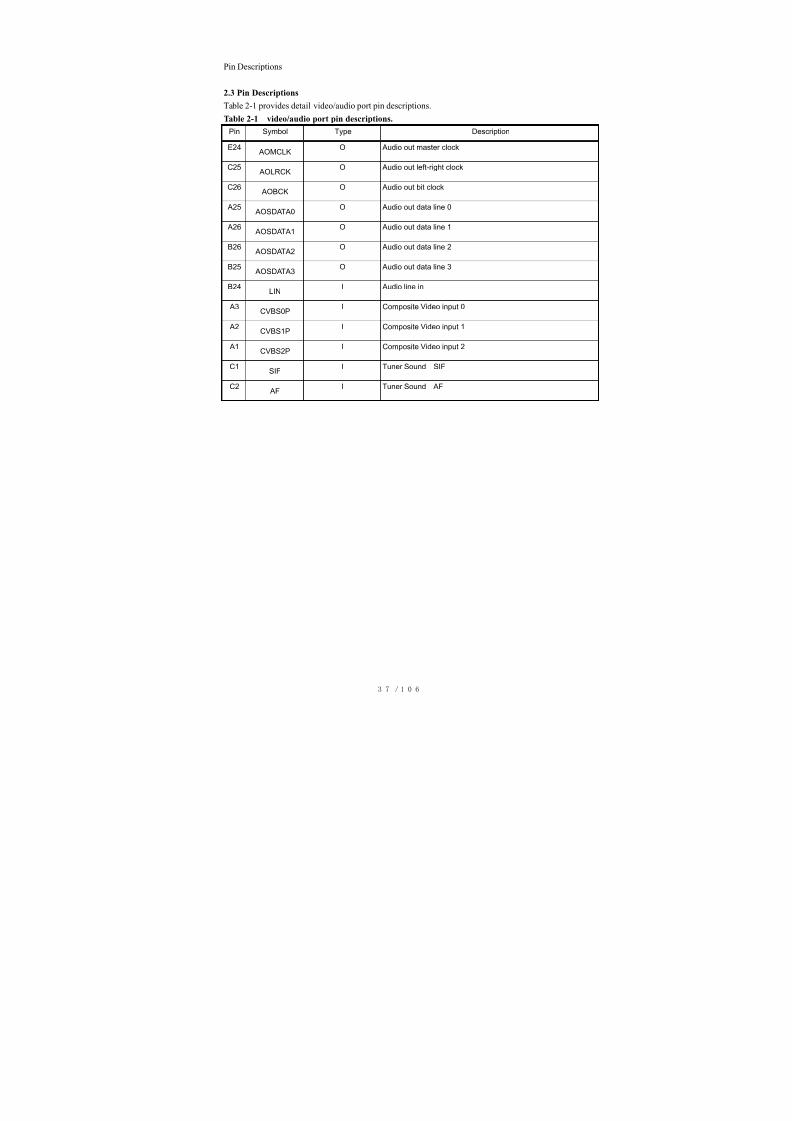
Pin Descriptions
2.3 Pin Descriptions
Table 2-1 provides detail video/audio port pin descriptions.
Table 2-1 video/audio port pin descriptions.
Pin Symbol Type Description
E24 AOMCLK
O Audio out master clock
C25 AOLRCK
O Audio out left-right clock
C26 AOBCK
O Audio out bit clock
A25 AOSDATA0
O Audio out data line 0
A26 AOSDATA1
O Audio out data line 1
B26 AOSDATA2 O Audio out data line 2
B25 AOSDATA3
O Audio out data line 3
B24LIN
I Audio line in
A3CVBS0P
I Composite Video input 0
A2CVBS1P
I Composite Video input 1
A1CVBS2P
I Composite Video input 2
C1SIF
I Tuner Sound SIF
C2 AF
I Tuner Sound AF
8/18/2019 Akai Lcd Tv Lct3201td_service Masnual
http://slidepdf.com/reader/full/akai-lcd-tv-lct3201tdservice-masnual 40/108
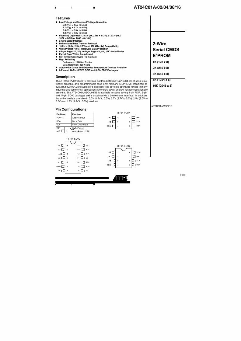
AT24C01A/2/4/8/16
2-Wire
Serial CMOS
E2PROM
1K (128 x 8)
2K (256 x 8)
4K (512 x 8)8K (1024 x 8)
16K (2048 x 8)
Features• Low Voltage and Standard Voltage Operation
5.0 (VCC = 4.5V to 5.5V)2.7 (VCC = 2.7V to 5.5V)
2.5 (VCC = 2.5V to 5.5V)
1.8 (VCC = 1.8V to 5.5V)
• Internally Organized 128 x 8 (1K), 256 x 8 (2K), 512 x 8 (4K),
1024 x 8 (8K) or 2048 x 8 (16K)
• 2-Wire Serial Interface
• Bidirectional Data Transfer Protocol
• 100 kHz (1.8V, 2.5V, 2.7V) and 400 kHz (5V) Compatibility
• Write Protect Pin for Hardware Data Protection
• 8-Byte Page (1K, 2K), 16-Byte Page (4K, 8K, 16K) Write Modes
• Partial Page Writes Are Allowed
• Self-Timed Write Cycle (10 ms max)
• High Reliability
Endurance: 1 Million Cycles
Data Retention: 100 Years
• Automotive Grade and Extended Temperature Devices Available
• 8-Pin and 14-Pin JEDEC SOIC and 8-Pin PDIP Packages
DescriptionThe AT24C01A/02/04/08/16 provides 1024/2048/4096/8192/16384 bits of serial elec-
trically erasable and programmable read only memory (EEPROM) organized as
128/256/512/1024/2048 words of 8 bits each. The device is optimized for use in many
industrial and commercial applications where low power and low voltage operation are
essential. The AT24C01A/02/04/08/16 is available in space saving 8-pin PDIP, 8-pinand 14-pin SOIC packages and is accessed via a 2-wire serial interface. In addition,
the entire family is available in 5.0V (4.5V to 5.5V), 2.7V (2.7V to 5.5V), 2.5V (2.5V to
5.5V) and 1.8V (1.8V to 5.5V) versions.
Pin Name Function
A0 to A2 Address Inputs
SDA Serial Data
SCL Serial Clock Input
WP Write Protect
NC No Connect
Pin Configurations
8-Pin PDIP
8-Pin SOIC
14-Pin SOIC
0180C
AT24C01A/02/04/08/16
32/75
8/18/2019 Akai Lcd Tv Lct3201td_service Masnual
http://slidepdf.com/reader/full/akai-lcd-tv-lct3201tdservice-masnual 41/108
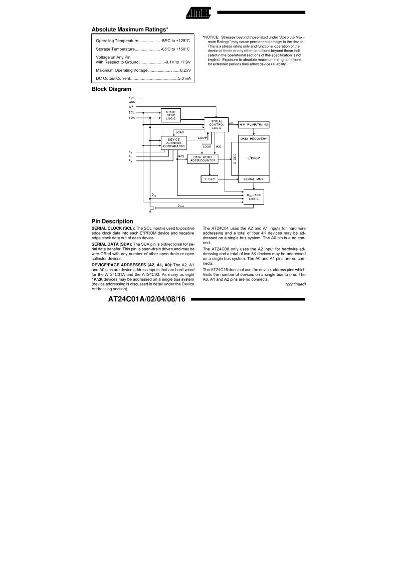
Block Diagram
Operating Temperature................... -55°C to +125°C
Storage Temperature...................... -65°C to +150°C
Voltage on Any Pin
with Respect to Ground ..................... -0.1V to +7.0V
Maximum Operating Voltage ........................... 6.25V
DC Output Current......................................... 5.0 mA
*NOTICE: Stresses beyond those listed under “Absolute Maxi-
mum Ratings” may cause permanent damage to the device.
This is a stress rating only and functional operation of the
device at these or any other conditions beyond those indi-
cated in the operational sections of this specification is not
implied. Exposure to absolute maximum rating conditions
for extended periods may affect device reliability.
Absolute Maximum Ratings*
Pin DescriptionSERIAL CLOCK (SCL): The SCL input is used to positive
edge clock data into each E2PROM device and negative
edge clock data out of each device.
SERIAL DATA (SDA): The SDA pin is bidirectional for se-
rial data transfer. This pin is open-drain driven and may bewire-ORed with any number of other open-drain or open
collector devices.
DEVICE/PAGE ADDRESSES (A2, A1, A0): The A2, A1and A0 pins are device address inputs that are hard wired
for the AT24C01A and the AT24C02. As many as eight
1K/2K devices may be addressed on a single bus system(device addressing is discussed in detail under the Device
Addressing section).
The AT24C04 uses the A2 and A1 inputs for hard wireaddressing and a total of four 4K devices may be ad-
dressed on a single bus system. The A0 pin is a no con-
nect.
The AT24C08 only uses the A2 input for hardwire ad-dressing and a total of two 8K devices may be addressed
on a single bus system. The A0 and A1 pins are no con-
nects.
The AT24C16 does not use the device address pins which
limits the number of devices on a single bus to one. The
A0, A1 and A2 pins are no connects.
(continued)
AT24C01A/02/04/08/16
33/75
8/18/2019 Akai Lcd Tv Lct3201td_service Masnual
http://slidepdf.com/reader/full/akai-lcd-tv-lct3201tdservice-masnual 42/108
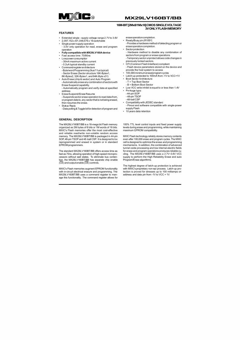
MX29LV160BT/BB
16M-BIT [2Mx8/1Mx16] CMOS SINGLE VOLTAGE
3V ONLY FLASH MEMORY
erase operation completion. Ready/Busy pin (RY/BY)
- Provides a hardware method of detecting program or
erase operation completion.
• Sector protection
- Hardware method to disable any combination of
sectors from program or erase operations
- Temporary sector unprotect allows code changes in
previously locked sectors.
• CFI (Common Flash Interface) compliant
- Flash device parameters stored on the device and
provide the host system to access
• 100,000 minimum erase/program cycles
• Latch-up protected to 100mA from -1V to VCC+1V• Boot Sector Architecture
- T = Top Boot Sector
- B = Bottom Boot Sector
• Low VCC write inhibit is equal to or less than 1.4V
• Package type:
- 44-pin SOP
- 48-pin TSOP
- 48-ball CSP
• Compatibility with JEDEC standard
- Pinout and software compatible with single-power
supply Flash
• 10 years data retention
FEATURES
• Extended single - supply voltage range 2.7V to 3.6V• 2,097,152 x 8/1,048,576 x 16 switchable
• Single power supply operation
- 3.0V only operation for read, erase and program
operation
• Fully compatible with MX29LV160A device
• Fast access time: 70/90ns
• Low power consumption
- 30mA maximum active current
- 0.2uA typical standby current
• Command register architecture
- Byte/word Programming (9us/11us typical)
- Sector Erase (Sector structure 16K-Bytex1,
8K-Bytex2, 32K-Bytex1, and 64K-Byte x31)
• Auto Erase (chip & sector) and Auto Program
- Automatically erase any combination of sectors with
Erase Suspend capability.
- Automatically program and verify data at specified
address
• Erase Suspend/Erase Resume
- Suspends sector erase operation to read data from,
or program data to, any sector that is not being erased,
then resumes the erase.
• Status Reply
- Data polling & Toggle bit for detection of program and
GENERAL DESCRIPTION
The MX29LV160BT/BB is a 16-mega bit Flash memory
organized as 2M bytes of 8 bits or 1M words of 16 bits.
MXIC's Flash memories offer the most cost-effective
and reliable read/write non-volatile random access
memory. The MX29LV160BT/BB is packaged in 44-pin
SOP, 48-pin TSOP and 48-ball CSP. It is designed to be
reprogrammed and erased in system or in standard
EPROM programmers.
The standard MX29LV160BT/BB offers access time asfast as 70ns, allowing operation of high-speed micropro-
cessors without wait states. To eliminate bus conten-
tion, the MX29LV160BT/BB has separate chip enable
(CE) and output enable (OE) controls.
MXIC's Flash memories augment EPROM functionality
with in-circuit electrical erasure and programming. The
MX29LV160BT/BB uses a command register to man-
age this functionality. The command register allows for
100% TTL level control inputs and fixed power supply
levels during erase and programming, while maintaining
maximum EPROM compatibility.
MXIC Flash technology reliably stores memory contents
even after 100,000 erase and program cycles. The MXIC
cell is designed to optimize the erase and programming
mechanisms. In addition, the combination of advanced
tunnel oxide processing and low internal electric fields
for erase and program operations produces reliable cy-cling. The MX29LV160BT/BB uses a 2.7V~3.6V VCC
supply to perform the High Reliability Erase and auto
Program/Erase algorithms.
The highest degree of latch-up protection is achieved
with MXIC's proprietary non-epi process. Latch-up pro-
tection is proved for stresses up to 100 milliamps on
address and data pin from -1V to VCC + 1V.
R
4
8/18/2019 Akai Lcd Tv Lct3201td_service Masnual
http://slidepdf.com/reader/full/akai-lcd-tv-lct3201tdservice-masnual 43/108
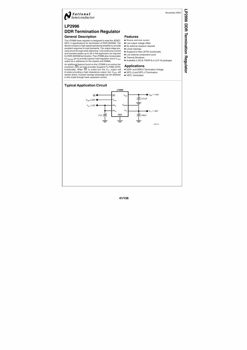
LP2996
DDR Termination RegulatorGeneral DescriptionThe LP2996 linear regulator is designed to meet the JEDEC
SSTL-2 specifications for termination of DDR-SDRAM. The
device contains a high-speed operational amplifier to provide
excellent response to load transients. The output stage pre-
vents shoot through while delivering 1.5A continuous current
and transient peaks up to 3A in the application as required
for DDR-SDRAM termination. The LP2996 also incorporates
a VSENSE pin to provide superior load regulation and a VREF
output as a reference for the chipset and DIMMs.
An additional feature found on the LP2996 is an active low
shutdown (SD) pin that provides Suspend To RAM (STR)
functionality. When SD is pulled low the VTT output will
tri-state providing a high impedance output, but, VREF will
remain active. A power savings advantage can be obtained
in this mode through lower quiescent current.
Featuresn Source and sink current
n Low output voltage offset
n No external resistors required
n Linear topology
n Suspend to Ram (STR) functionality
n Low external component count
n Thermal Shutdown
n Available in SO-8, PSOP-8 or LLP-16 packages
Applicationsn DDR-I and DDR-II Termination Voltage
n SSTL-2 and SSTL-3 Termination
n HSTL Termination
Typical Application Circuit
20057518
November 2003
L P 2 9 9 6 D D R
T er mi n a t i onR e g ul a t or
41/106
8/18/2019 Akai Lcd Tv Lct3201td_service Masnual
http://slidepdf.com/reader/full/akai-lcd-tv-lct3201tdservice-masnual 44/108
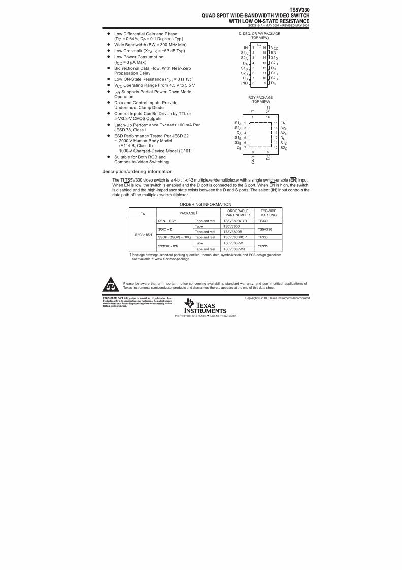
SCDS164A – MAY 2004 − REVISED MAY 2004
POST OFFICE BOX 655303 • DALLAS, TEXAS 75265
Low Differential Gain and Phase
(DG = 0.64%, DP = 0.1 Degrees Typ)
Wide Bandwidth (BW = 300 MHz Min)
Low Crosstalk (XTALK = −63 dB Typ)
Low Power Consumpt ion
(ICC = 3 µ A Max) Bidi rectional Data Flow, With Near-Zero
Propagation Delay
Low ON-State Resistance (r on = 3 Ω Typ)
VCC Operating Range From 4.5 V to 5.5 V
Iof f Supports Partial-Power-Down Mode
Operation
Data and Control Inputs Provide
Undershoot Clamp Diode
Control Inputs Can Be Driven by TTL or
5-V/3.3-V CMOS Outputs
Latch-Up Performance Exceeds 100 mA Per JESD 78, Class II
ESD Performance Tested Per JESD 22
− 2000-V Human-Body Model
(A114-B, Class II)
− 1000-V Charged-Device Model (C101)
Suitable for Both RGB and
Composite-Video Switching
description/ordering information
The TI TS5V330 video switch is a 4-bit 1-of-2 multiplexer/demultiplexer with a single switch-enable (EN) input.
When EN is low, the switch is enabled and the D port is connected to the S port. When EN is high, the switch
is disabled and the high-impedance state exists between the D and S ports. The select (IN) input controls thedata path of the multiplexer/demultiplexer.
ORDERING INFORMATION
T A PACKAGE† ORDERABLE
PART NUMBER
TOP-SIDE
MARKING
QFN − RGY Tape and reel TS5V330RGYR TE330
Tube TS5V330D
SOIC − DTape and reel TS5V330DR
TS5V330
−40°C to 85°CSSOP (QSOP) − DBQ Tape and reel TS5V330DBQR TE330
−Tube TS5V330PW
TSSOP − PWTape and reel TS5V330PWR
TE330
† Package drawings, standard packing quantities, thermal data, symbolization, and PCB design guidelines
are available at www.ti.com/sc/package.
Copyright© 2004, Texas Instruments Incorporated
Please be aware that an important notice concerning availability, standard warranty, and use in critical applications of
Texas Instruments semiconductor products and disclaimers thereto appears at the end of this data sheet.
D
D, DBQ, OR PW PACKAGE
(TOP VIEW)
RGY PACKAGE
(TOP VIEW)
1 16
8 9
2
3
4
5
6
7
15
14
13
12
11
10
EN
S2D
S2D
DD
S1C
S2C
S1 AS2 AD A
S1B
S2B
DB
I N V
G N D
C C
1
2
3
45
6
7
8
16
15
14
1312
11
10
9
IN
S1 AS2 A
D A
S1B
S2B
DB
GND
VCC
EN
S1D
S2DDD
S1C
S2C
DC
C
36/75
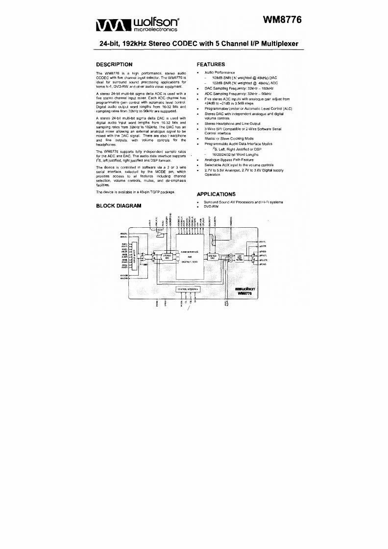
8/18/2019 Akai Lcd Tv Lct3201td_service Masnual
http://slidepdf.com/reader/full/akai-lcd-tv-lct3201tdservice-masnual 45/108/
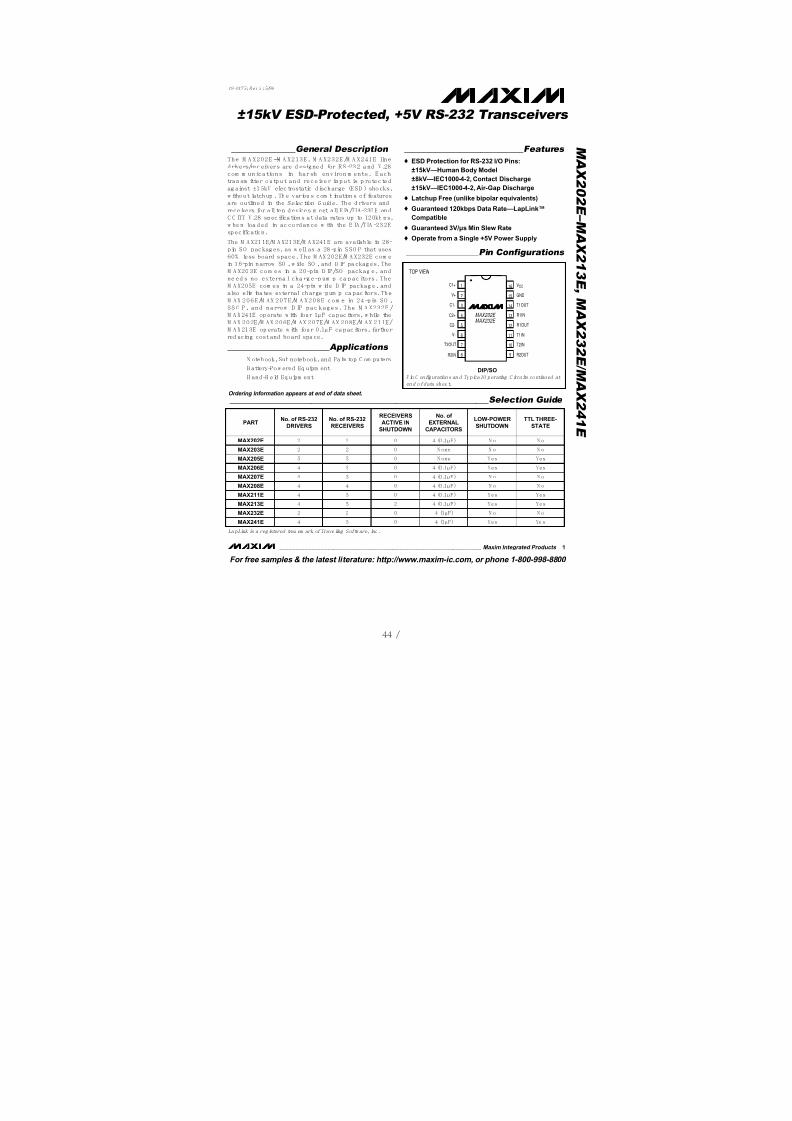
8/18/2019 Akai Lcd Tv Lct3201td_service Masnual
http://slidepdf.com/reader/full/akai-lcd-tv-lct3201tdservice-masnual 46/108
_______________General Description The M A X202E–M A X213E, M A X232E /M A X241E linedrivers/rec eivers are d esigne d for RS-23 2 a nd V.28com m un ications in harsh environ m ents. E achtransm itter outp ut and receive r inp ut is p rotected
ag ainst ±1 5kV electrostatic discharge (ESD ) shocks,w ithout latchup . The various com binations of featuresare outlined in the Selection G uide. The d rivers and
receivers for all ten d evices m eet all EIA /TIA-232E andC C ITT V.28 specifications at data rates up to 120kb ps,w hen load ed in ac co rdan ce w ith the E IA /TIA -23 2E
sp ecification.
The M A X211E/M A X213E/M A X241E are available in 28-
pin SO packages, as w ell as a 28-pin SSO P that uses60% less board space. The M AX 202E/M A X232E com ein 16-pin narrow SO , w ide SO , and D IP packages. TheM A X20 3E co m es in a 20-pin D IP/SO packag e, and
ne ed s no externa l cha rg e-p um p ca p ac itors. TheM A X205E com es in a 24-pin w ide D IP packag e, andalso elim inates external charge-pum p capacitors. The
M AX 206E/M AX 207E/M A X208E com e in 24-pin SO ,SS O P, and narrow D IP pac kages. The M A X232E /M A X241E op erate w ith four 1µF capacitors, w hile the
M AX 202E/M AX 206E/M AX 207E/M AX 208E/M AX 211E/M A X213E op erate w ith four 0.1µF capacitors, furtherreducing cost and board space.
________________________Applications
N otebook, Sub notebook, and Palm top C om puters
B attery-Pow ered Eq uipm ent
H and-H eld Eq uipm ent
____________________________Features
ESD Protection for RS-232 I/O Pins:
±15kV—Human Body Model
±8kV—IEC1000-4-2, Contact Discharge
±15kV—IEC1000-4-2, Air-Gap Discharge
Latchup Free (unlike bipolar equivalents)
Guaranteed 120kbps Data Rate—LapLink™
Compatible
Guaranteed 3V/µs Min Slew Rate
Operate from a Single +5V Power Supply
MAX2 0 2 E–MAX2 1 3 E ,MAX2 3 2 E / MAX2 4 1 E
±15kV ESD-Protected, +5V RS-232 Transceivers
________________________________________________________________ Maxim Integrated Products 1
16
15
14
13
12
11
10
9
1
2
3
4
5
6
7
8
VCC
GND
T1OUT
R1INC2+
C1-
V+
C1+
TOP VIEW
MAX202E
MAX232E R1OUT
T1IN
T2IN
R2OUTR2IN
T2OUT
V-
C2-
DIP/SO
_________________Pin Configurations
_____________________________________________________________Selection Guide
19-0175; Rev 3; 5/96
La pLink is a registered trad em ark of Traveling Softw are, Inc.
Pin C onfigurations an d Typical O perating C ircuits continued at
end of data sheet.
Ordering Information appears at end of data sheet.
For free samples & the latest literature: http://www.maxim-ic.com, or phone 1-800-998-8800
Ye s
PARTNo. of RS-232
DRIVERS
No. of RS-232
RECEIVERS
RECEIVERS
ACTIVE IN
SHUTDOWN
No. of
EXTERNAL
CAPACITORS
LOW-POWER
SHUTDOWN
TTL THREE-
STATE
MAX202E 2 2 0 4 (0.1µF) N o N o
MAX203E 2 2 0 N one N o N o
MAX205E 5 5 0 N one Yes Yes
MAX206E 4 3 0 4 (0.1µF) Yes Yes
MAX207E 5 3 0 4 (0.1µF) N o N o
MAX208E 4 4 0 4 (0.1µF) N o N o
MAX211E 4 5 0 4 (0.1µF) Yes YesMAX213E 4 5 2 4 (0.1µF) Yes Yes
MAX232E 2 2 0 4 (1µF) N o N o
MAX241E 4 5 0 4 (1µF) Yes
44/
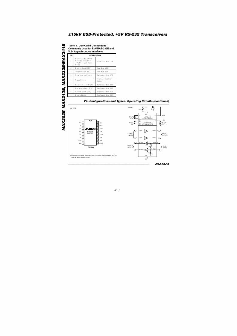
8/18/2019 Akai Lcd Tv Lct3201td_service Masnual
http://slidepdf.com/reader/full/akai-lcd-tv-lct3201tdservice-masnual 47/108
M A X 2 0 2 E – M
A X 2 1 3 E ,
M A X 2 3 2 E / M A X 2 4 1 E
±15kV ESD-Protected, +5V RS-232 Transceivers
______________________________________________________________________________________
____________Pin Configurations and Typical Operating Circuits (continued)
TOP VIEW
1
4
5
TTL/CMOS
INPUTS
TTL/CMOS
OUTPUTS
11
10
12
9
3
GND
C1-
C2+
5k
5k
C2-
T1IN
T2IN
R2OUT
R1OUT
VCC
+5V TO +10V
VOLTAGE DOUBLER
+10V TO -10V
VOLTAGE IN VERTER
16
2
6
14
7
13
8
0.1µF
0.1µF*16V
0.1µF*6.3V
0.1µF*16V
0.1µF*6.3V
C1+
RS-232
OUTPUTS
RS-232
INPUTS
-10V
+10VV+
+5V INPUT
V-
T1OUT
R1IN
R2IN
T2OUT
T1
15
T2
R1
R2
PIN NUM BERS ON TYPICAL OPERATING CIRCUIT REFER TO DI P/SO PACKAGE, NOT LCC.
* 1.0µF CAPACITORS, MAX232E ONLY.
16
15
14
13
12
11
10
9
1
2
3
4
5
6
7
8
VCC
GND
T1OUT
R1INC2+
C1-
V+
C1+
MAX202E
MAX232E R1OUT
T1IN
T2IN
R2OUTR2IN
T2OUT
V-
C2-
DIP/SO
Table 3. DB9 Cable Connections
Commonly Used for EIA/TIAE-232E and
V.24 Asynchronous Interfaces
PIN CONNECTION
2 R eceive D ata (R D) D ata from D C E
3 Transm it D ata (TD ) D ata from D TE
4 D ata Term inal R ead y H and shake from D TE
5 S ig nal G roundR eference point for
signals
6 D ata S et R ead y (D S R ) H and shake from D C E
7 R eq uest to Send (R TS ) H a nd shake from D T E
8 C lear to S end (C TS ) H andshake from D C E
9 R ing Indicator H andshake from D CE
1
R eceived Line Signal
D etector (som etim es
called C arrier D etect,
D C D )
H andshake from D C E
45/
8/18/2019 Akai Lcd Tv Lct3201td_service Masnual
http://slidepdf.com/reader/full/akai-lcd-tv-lct3201tdservice-masnual 48/108
MEGMEET
MEGMEET ELECTRICAL TECHNOLOGY CO. LTD.
DESCRIPTION:
SPECIFICATION
THESE SPECIFICATION ARE THE PROPERTY OF MEGMEET ELECTRICAL TECHNOLOGY CO., LTD
AND SHALL NOT BE REPRODUCED OR USED AS THE BASIS FOR THE MANUFACTURE OR SELL
Model No.:
Meet with mega satisfaction
SPECIFICATION FOR APPROVAL
Part No. MLT186A
Description: LCD Power Supply Specification
Revision: 1.0
Customer. SANSUI ELECTRIC
Customer Approval No. :
Please return to us one original of “SPECIFICATION FOR APPROVAL” with your approved signatures.
APPROVED SIGNATURES
APPROVED BY: DATE:
CHOP & SIGNATURES:
SHENZHEN MEGMEET ELECTRICAL TECHNOLOGY CO.,LTD
Add: 6F Tower 2, Zhongjian Industrial Building
18 Yanshan Road , Shekou, Shenzhen, P.R.China
ZIP CODE:518067
TEL: (0755)26693042 26693442
FAX: (0755)26693047
E-mail: [email protected]
8/18/2019 Akai Lcd Tv Lct3201td_service Masnual
http://slidepdf.com/reader/full/akai-lcd-tv-lct3201tdservice-masnual 49/108
MEGMEET
MEGMEET ELECTRICAL TECHNOLOGY CO. LTD.
DESCRIPTION:
SPECIFICATION
THESE SPECIFICATION ARE THE PROPERTY OF MEGMEET ELECTRICAL TECHNOLOGY CO., LTD
AND SHALL NOT BE REPRODUCED OR USED AS THE BASIS FOR THE MANUFACTURE OR SELL
Model No.:
Spec.
Rev.
Sample
Rev.
Date Description Safety
by
Mechanical
by
Electrical
by
1.0 1.02005.
09.12
Zhangzhi Qiu Tony Yang
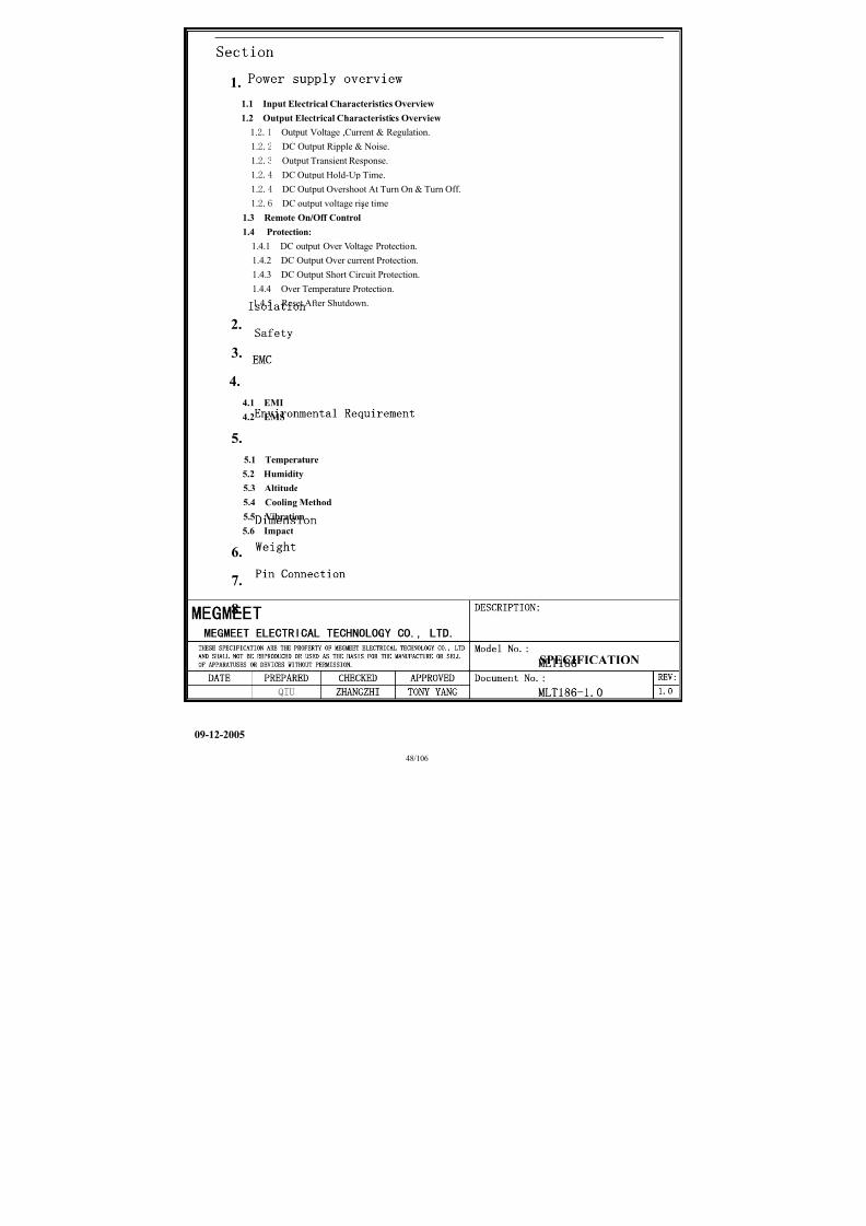
8/18/2019 Akai Lcd Tv Lct3201td_service Masnual
http://slidepdf.com/reader/full/akai-lcd-tv-lct3201tdservice-masnual 50/108
MEGMEET
MEGMEET ELECTRICAL TECHNOLOGY CO. LTD.
DESCRIPTION:
SPECIFICATION
THESE SPECIFICATION ARE THE PROPERTY OF MEGMEET ELECTRICAL TECHNOLOGY CO., LTD
AND SHALL NOT BE REPRODUCED OR USED AS THE BASIS FOR THE MANUFACTURE OR SELL
Model No.:
Section
1. Power supply overview
1.1 Input Electrical Characteristics Overview
1.2 Output Electrical Characteristics Overview
1.2.1 Output Voltage ,Current & Regulation. 1.2.2 DC Output Ripple & Noise.
1.2.3 Output Transient Response.
1.2.4 DC Output Hold-Up Time.
1.2.4 DC Output Overshoot At Turn On & Turn Off.
1.2.6 DC output voltage rise time
1.3 Remote On/Off Control:
1.4 Protection:
1.4.1 DC output Over Voltage Protection.
1.4.2 DC Output Over current Protection.
1.4.3 DC Output Short Circuit Protection.
1.4.4 Over Temperature Protection.
1.4.5 Reset After Shutdown.
2. Isolation
3. Safety
4. EMC
4.1 EMI4.2 EMS
5. Environmental Requirement
5.1 Temperature
5.2 Humidity
5.3 Altitude
5.4 Cooling Method
5.5 Vibration
5.6 Impact
6. Dimension
7. Weight
8. Pin Connection

8/18/2019 Akai Lcd Tv Lct3201td_service Masnual
http://slidepdf.com/reader/full/akai-lcd-tv-lct3201tdservice-masnual 51/108
MEGMEET
MEGMEET ELECTRICAL TECHNOLOGY CO. LTD.
DESCRIPTION:
SPECIFICATION
THESE SPECIFICATION ARE THE PROPERTY OF MEGMEET ELECTRICAL TECHNOLOGY CO., LTD
AND SHALL NOT BE REPRODUCED OR USED AS THE BASIS FOR THE MANUFACTURE OR SELL
Model No.:
Spec.
Rev.
Sample
Rev.
Date Description Safety
by
Mechanical
by
Electrical
by
1.0 1.02005.
09.12
Zhangzhi Qiu Tony Yang
8/18/2019 Akai Lcd Tv Lct3201td_service Masnual
http://slidepdf.com/reader/full/akai-lcd-tv-lct3201tdservice-masnual 52/108
MEGMEET
MEGMEET ELECTRICAL TECHNOLOGY CO. LTD.
DESCRIPTION:
SPECIFICATION
THESE SPECIFICATION ARE THE PROPERTY OF MEGMEET ELECTRICAL TECHNOLOGY CO., LTD
AND SHALL NOT BE REPRODUCED OR USED AS THE BASIS FOR THE MANUFACTURE OR SELL
Model No.:
2) Outputs shall be bypassed at the connector with a 0.1uF ceramic capacitor and a
10uF electrolytic capacitor to simulate system loading.
1.2.3 Output Transient Response.
Table 4. Test condition.Voltage Tolerance Limit Slew Rate Load Change
V1/V3±5%
+V2 ±10%
+5V±5%
+5.1VSB±5%
0.2A/uS Min. to 50% load and 50% to Max load
all outputs ±10% 0.2A/uS Min. load to Max load
Note: Transient response measurements shall be made with a load changing repetition
rate of 50Hz to 10kHz.
1.2.4 Table 5 DC Output Hold-Up Time.
Output Voltage 120Vac input 220Vac input
+V1/+V2(+24V) ≥10 mS ≥10 mS
+V3(+12V) ≥10 mS ≥10 mS
+5V/+5.1VSB ≥10 mS ≥10 mS
Note: All of dc output at full load.
1.2.5 Table 6 DC Output Overshoot At Turn On & Turn Off.
Over shoot voltage(V) Output Channel Output(V)
Turn on Turn off
+V1 +24V 2% 2%
+V2 +24V 5% 5%
+V3 + 12V 2% 2%
+5V +5V 5% 5%
+5.1VSB +5.1V 5% 5%
Note: All of dc output current from Min. to Max.
1.2.6 Table 7 DC output voltage rise time
Output Voltage 120Vac input &Full Load 220Vac input &Full Load
+V1/+V2(+24V) ≤100 mS ≤100 mS
8/18/2019 Akai Lcd Tv Lct3201td_service Masnual
http://slidepdf.com/reader/full/akai-lcd-tv-lct3201tdservice-masnual 53/108
MEGMEET
MEGMEET ELECTRICAL TECHNOLOGY CO. LTD.
DESCRIPTION:
SPECIFICATION
THESE SPECIFICATION ARE THE PROPERTY OF MEGMEET ELECTRICAL TECHNOLOGY CO., LTD
AND SHALL NOT BE REPRODUCED OR USED AS THE BASIS FOR THE MANUFACTURE OR SELL
Model No.:
+V3(+12V) ≤100 mS ≤100 mS
+5V ≤100 mS ≤100 mS
+5.1VSB ≤100 mS ≤100 mS
Note: The output voltages shall rise from10% to 90% of their output voltage.
1.3 Remote On/Off Control:
The power supply DC outputs (without +5.1Vsb) shall be enable with an active-high
TTL(≥2.0V/2.0mA)-compatible signal(Ps-on). The +5.1Vsb is on whenever the AC
power is present.
* When Ps-on is pulled to TTL high, the DC outputs are to be enabled.
* When Ps-on is pulled to TTL low or open circuit, the DC outputs are to be disabled.
Table 8.
Ps-on Signal Comments Outputs
Ps-on- high ≥2.5V&2.0mA ( source) Enable
Ps-on- low ≤1.5 V X
Ps-on-open -- X
1.4 Protection:
1.4.1 Table 9 DC output Over Voltage Protection.
Output Voltage Max. Over Voltage Comments
+V1(+24V) 28V Power supply latch into shutdown state
+5.0V 7Vtyp Hiccup
Note: The power supply shall be test at max AC voltage (270Vac) and min load or no load.
1.4.2 Table 10 DC Output Over current Protection.
Output Voltage Over Current Comments
8/18/2019 Akai Lcd Tv Lct3201td_service Masnual
http://slidepdf.com/reader/full/akai-lcd-tv-lct3201tdservice-masnual 54/108
MEGMEET
MEGMEET ELECTRICAL TECHNOLOGY CO. LTD.
DESCRIPTION:
SPECIFICATION
THESE SPECIFICATION ARE THE PROPERTY OF MEGMEET ELECTRICAL TECHNOLOGY CO., LTD
AND SHALL NOT BE REPRODUCED OR USED AS THE BASIS FOR THE MANUFACTURE OR SELL
Model No.:
+V1(+24V) ≥7Atyp Shutdown
+V2(+24V) ≥2Atyp Shutdown
+V3(+12V) ≥3A Shutdown
+5V/+5.1VSB ≥9A type Hiccup
1.4.3 Table 11 DC Output Short Circuit Protection.
Output Voltage Comments
+V1(+24V) Shutdown
+V2(+24V) Shutdown
+V3(+12V) Shutdown
+5V/5.1VSB Hiccup
1.4.4 Reset After Shutdown.
Recycle the ps-on signal, the power supply will restart after the fault removed.
2. Isolation
2.1 Table 12
Input To Output DC500V 50MΩmin (at room temperature)
Input To FG DC500V 50MΩmin (at room temperature)
Output To FG Non Isolated
2.2 Table 13
Input To Output 3000Vac 50Hz 1minute ≤10mA
Input To FG 1500Vac 50Hz 1minute ≤10mA
Output To FG Non Isolated
Note: Open FG and Output return.
3.
Safety
The power supply shall compliance with the following Criterion:
1) UL60950
2) EN60950
3) GB4943-1995/GB8898-2001
8/18/2019 Akai Lcd Tv Lct3201td_service Masnual
http://slidepdf.com/reader/full/akai-lcd-tv-lct3201tdservice-masnual 55/108
MEGMEET
MEGMEET ELECTRICAL TECHNOLOGY CO. LTD.
DESCRIPTION:
SPECIFICATION
THESE SPECIFICATION ARE THE PROPERTY OF MEGMEET ELECTRICAL TECHNOLOGY CO., LTD
AND SHALL NOT BE REPRODUCED OR USED AS THE BASIS FOR THE MANUFACTURE OR SELL
Model No.:
4.
EMC
4.1 EMI
The power supply shall compliance with the following Criterion:
1 Conduction Emission :
*EN55013, CLASS B*GB13837-2003, CLASS B
*CISPR13:2001
2 Radiated Emission :
*EN55013, CLASS B
*GB13837-2003, CLASS B
*CISPR13:2001
4.2 EMS
The power supply shall compliance with the following Criterion:
1 ESD
*GB17626.2-1998/IEC61000-4-2 Lever 3
2 EFT
*GB17626.4-1998/IEC61000-4-4 Lever 3
3 SURGE
*GB17626.5-1998/IEC61000-4-5 Lever 3
4)
DIP
*GB17626.11-1998/IEC61000-4-11 Class B/C
5. Environmental Requirement
5.1 Temperature
* Operating: -10 to +50.
* Store: -20 to +80.
5.2 Humidity
* Operating: From 10%to90% relative humidity (non-condensing).
* Store: From 5 to 95% relative humidity (non-condensing).
5.3 Altitude
* Operating: to10,000 ft.
* Store: to 20,000ft.
5.4 Cooling Method
* Ventilation cooling .
5.5 Vibration
* 10-55Hz, 49.0m/s²(5G), 3minutes period, 20minutes each along X, Y and Z axis.
5.6 Impact
* 196.1m/s²(20G),11ms, once each X, Y and Z axis.
8/18/2019 Akai Lcd Tv Lct3201td_service Masnual
http://slidepdf.com/reader/full/akai-lcd-tv-lct3201tdservice-masnual 56/108
MEGMEET
MEGMEET ELECTRICAL TECHNOLOGY CO. LTD.
DESCRIPTION:
SPECIFICATION
THESE SPECIFICATION ARE THE PROPERTY OF MEGMEET ELECTRICAL TECHNOLOGY CO., LTD
AND SHALL NOT BE REPRODUCED OR USED AS THE BASIS FOR THE MANUFACTURE OR SELL
Model No.:
6. Dimension
* 200mm X 130mm X 25mm (L *W * H ).
7. Weight
* 680g
8. Pin Connection
Table 15 CN3 VENTER:
NO. Pin Connection Function
1 +24VAUDIO +24VDC OUTPUT
2 +24VAUDIO +24VDC OUTPUT
3 GND +24VDC RETURN
4 GND +24VDC RETURN
Note: CN3 -- JST VA CONNEETION, TYPE : pitch:2.0mm
Table 16 CN2 VENTER:
NO. Pin Connection Function
1 +24V +24VDC OUTPUT
2 +24V +24VDC OUTPUT
3 +24V +24VDC OUTPUT
4 +24V +24VDC OUTPUT
5 GND +24VDC RETURN
6 GND +24VDC RETURN
7 GND +24VDC RETURN
8 GND +24VDC RETURN
Note: CN2 -- JST VA CONNEETION, TYPE : pitch:2.54mm
Table 17 CN1 VENTER:
NO. Pin Connection Function
1 +12V +12DC OUTPUT2 +12V +12DC OUTPUT
3 +12V +12DC OUTPUT
4 GND +12V/+5VDC RETURN
5 GND +12V/+5VDC RETURN

8/18/2019 Akai Lcd Tv Lct3201td_service Masnual
http://slidepdf.com/reader/full/akai-lcd-tv-lct3201tdservice-masnual 57/108
MEGMEET
MEGMEET ELECTRICAL TECHNOLOGY CO. LTD.
DESCRIPTION:
SPECIFICATION
THESE SPECIFICATION ARE THE PROPERTY OF MEGMEET ELECTRICAL TECHNOLOGY CO., LTD
AND SHALL NOT BE REPRODUCED OR USED AS THE BASIS FOR THE MANUFACTURE OR SELL
Model No.:
6 GND +12V/+5VDC RETURN
7 +5V +5DC OUTPUT
8 +5V +5DC OUTPUT
9 +5V +5DC OUTPUT
10 +5V +5DC OUTPUT
11 +5V +5DC OUTPUT
Note: CN2 -- JST VA CONNEETION, TYPE : pitch:2.0mm
Table 15 CN4 VENTER:
NO. Pin Connection Function
1 +5VSB +5VSB OUTPUT
2 +5VSB +5VSB OUTPUT
3 GND +5VSB RETURN
4 GND +5VSB RETURN
5 PS-ON PS-ON
Note: CN3 -- JST VA CONNEETION, TYPE : pitch:2.0mm
Table 18 CON1 VENTER:
NO. Pin Connection Function
① AC-L AC INPUT LINE
② NC NC③ AC-N AC INPUT NUTURE
Note: CN3 -- JST VA CONNEETION, TYPE : pitch:3.96mm
Fig.8.1 Pin Connection (Top View)
8/18/2019 Akai Lcd Tv Lct3201td_service Masnual
http://slidepdf.com/reader/full/akai-lcd-tv-lct3201tdservice-masnual 58/108
MEGMEET
MEGMEET ELECTRICAL TECHNOLOGY CO. LTD.
DESCRIPTION:
SPECIFICATION
THESE SPECIFICATION ARE THE PROPERTY OF MEGMEET ELECTRICAL TECHNOLOGY CO., LTD
AND SHALL NOT BE REPRODUCED OR USED AS THE BASIS FOR THE MANUFACTURE OR SELL
Model No.:
8/18/2019 Akai Lcd Tv Lct3201td_service Masnual
http://slidepdf.com/reader/full/akai-lcd-tv-lct3201tdservice-masnual 59/108
MEGMEET
MEGMEET ELECTRICAL TECHNOLOGY CO. LTD.
DESCRIPTION:
SPECIFICATION
THESE SPECIFICATION ARE THE PROPERTY OF MEGMEET ELECTRICAL TECHNOLOGY CO., LTD
AND SHALL NOT BE REPRODUCED OR USED AS THE BASIS FOR THE MANUFACTURE OR SELL
Model No.:
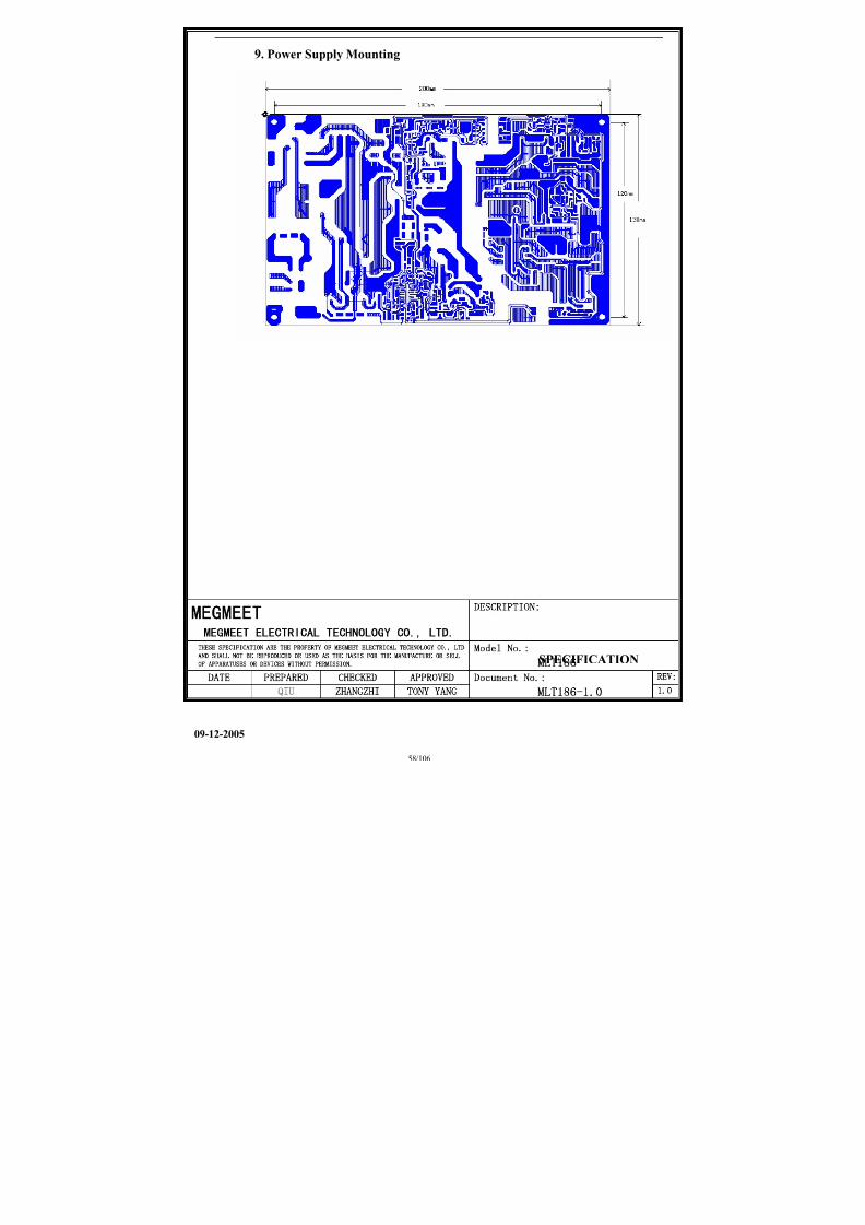
8/18/2019 Akai Lcd Tv Lct3201td_service Masnual
http://slidepdf.com/reader/full/akai-lcd-tv-lct3201tdservice-masnual 60/108
MEGMEET
MEGMEET ELECTRICAL TECHNOLOGY CO. LTD.
DESCRIPTION:
SPECIFICATION
THESE SPECIFICATION ARE THE PROPERTY OF MEGMEET ELECTRICAL TECHNOLOGY CO., LTD
AND SHALL NOT BE REPRODUCED OR USED AS THE BASIS FOR THE MANUFACTURE OR SELL
Model No.:
9. Power Supply Mounting
8/18/2019 Akai Lcd Tv Lct3201td_service Masnual
http://slidepdf.com/reader/full/akai-lcd-tv-lct3201tdservice-masnual 61/108
P r o d u c t S p e c i f i c a t i o n Ver05 DL-06
SPECIFICATION
CUSTOMER:
DESCRIPTION: Slot-in DVD LOADER
MODEL: DL-06 series(DL-06**)
CUSTOMER APPROVED
ISSUE DATE:2005.11.02
Approved Checked by
Sales Dept.
Checked by
Technical Dept.Prepared
8/18/2019 Akai Lcd Tv Lct3201td_service Masnual
http://slidepdf.com/reader/full/akai-lcd-tv-lct3201tdservice-masnual 62/108
Prod uctS pecif icationVer05 DL-06
1. Scope
1.1This specification applies to Slot-in DVD mechanism for DVD player (thereafter called DVD
mechanism ). Foryou model : DL-06**.
1.2 Any query over the specification shall be expressed by R&D dept. of Foryou Multimedia
Electronics Co.,Ltd.
1.3 For improving performance purpose, this specification is subject to change according to
pre-agreement established between us.
1.4 Hardware and software or manufacturing process may subject to change for improvements
within the rang of the specifications.
2. Dimension of shell and installation
2.1 See attachment for details of dimension of shell and installation.
3. General specification
3.1 Mechanism
3.1.1 Disc loading: Motorized loading.
3.1.2 Disc ejecting: Motorized ejection.
3.1.3 Play: Loading→
auto play
3.1.4 Skew adjusting: adjust two points on the base of spindle motor.
3.1.5 Pick-up feed mode: gear and rack drive.
3.1.6 Range of pick-up movement: 22.5mm ~ 59mm, from the center of spindle motor.
8/18/2019 Akai Lcd Tv Lct3201td_service Masnual
http://slidepdf.com/reader/full/akai-lcd-tv-lct3201tdservice-masnual 63/108
P r o d u c t S p e c i f i c a t i o n Ver05 DL-06
3.1.7
Anti vibration: two steps of dampers to reduce the vibration.
3.2 Power supply
DC12 ±1V(600 mA)& DC5±0.2V (660 mA) .
3.3 Pick-up
3.3.1 Pick-up : PVR-520T、PVR-502W(MITSUMI)、HOP-1200S(W)(HITACHI)、
OPU-3153(SANKYO)、SF-HD62(SANYO)、SF-HD65(SANYO)two laser diode a
single object lens pickup.
3.4 Motor
Spindle motor: DC brush motor: CCM03-030R1-26O ( (Moretech).3.4.1
3.4.2 Sled motor : WRF-300CA-09600.
3.4.3 Loading motor : WFF-050SB-10200.
3.5 Detect switch
3.5.1 Pick-up inner position detecting SW: (WI-A278)、(DS3-A-0001)
3.5.2 Disc chucking detecting SW: ESE22 (Type B)×1pcs
3.5.3 Disc detecting SW: ESE22 (Type B)×2pcs (Panasonic).
3.6 Weight: approximate 476 g.
4. General performance
4.1 Disc specification
Diameter of disc:Φ120±0.3,Φ80±0.3
Thickness of Disc:1.2(+0.3,-0.1)
Type of disc:

8/18/2019 Akai Lcd Tv Lct3201td_service Masnual
http://slidepdf.com/reader/full/akai-lcd-tv-lct3201tdservice-masnual 64/108
Prod uctS pecif icationVer05 DL-06
DVD Video;
CD-DA;
Video CD;
CD-R, CD-RW;
4.2
Prevention from the 2nd
disc insertion: the second disc can’t be loaded when there is a disc in
mechanism.
4.3
Noise Spec. ≤65 dB( A)
Noise level tests shall be carried out in an anechoic room with background noise 20 dB( A) or
less.Noise shall be measured at a position 10cm from the front of the mechanical section.
5. Conditions of operation and storage
5.1 Operation temperature range: 0 ~ + 45 .
5.2 Range of storage: -20 ~ + 60
5.3 Operation moisture range: 10% ~ 80% RH.
5.4 Storage moisture range: 0% ~ 90% RH.
5.5 Atmospheric pressure: 860mBar ~ 1060 mBar.
6. Condition of performance evaluation
6.1 Installation: see attachment. Tightened on work table; Installation angle:
forth and back: ±10 º, left and right: ±10 º.
6.2 Environment of evaluation
:25±2 Temperature
:60±5%(RH) Humidity
But,
8/18/2019 Akai Lcd Tv Lct3201td_service Masnual
http://slidepdf.com/reader/full/akai-lcd-tv-lct3201tdservice-masnual 65/108
P r o d u c t S p e c i f i c a t i o n Ver05 DL-06
:+15 ~ +30 Temperature
:45% ~ 75%RHHumidity
Noise: in an anechoic room with background noise 20dB (A) or less.
6.3 Test circuit and equipment
6.3.1
Refer FORYOU’s standard circuit and equivalent.
7. Reliability test
7.1 Environment test
Item Specification
7.1.1
Test of high temperature
storage After 24hours kept at +60 , and then 16 hours at room temperature,
the mechanism shall be able to load/eject and playback within thisprocess.(Test disc:TCD-792 and TDV-520A)
7.1.2
Test of low temperature
storage After 24hours kept at -20 , and then 16 hours at room temperature,
the mechanism shall be able to load/eject and playback within this
process.(Test disc:TCD-792 and TDV-520A)
7.1.3
Test of high temperatureand high moisture storage After 48hours kept at +40 , 90%RH, and then 16 hours at ro om
temperature, the mechanism shall be able to load/eject and
playback within this process.(Test disc:TCD-792 and TDV-520A)
8/18/2019 Akai Lcd Tv Lct3201td_service Masnual
http://slidepdf.com/reader/full/akai-lcd-tv-lct3201tdservice-masnual 66/108
P r o d u c t S p e c i f i c a t i o n Ver05 DL-06
7.1.4
High and low temperature
cycling test Applied -20(1H)←→60(1H)(temperature slope 80/H),
5cycles,then place at normal temperature for 16 hours, the mechanism
shall be able to load/eject and playback within this process.(Test
disc:TCD-792 and TDV-520A)
7.1.5
Test of high temperature
operation
DVD mechanism shall be kept in 45 for 4 hours, and then operate,
the mechanism shall be able to load/eject and playback within this
process.(Test disc:TCD-792 and TDV-520A)
7.1.6
DVD mechanism shall be kept in 0 for 4 hours, and then operate,
the mechanism shall be able to load/eject and playback within this
process.(Test disc:TCD-792 and TDV-520A)
Test of low temperature
operation
7.2 Life test
Item Specification
7.2.1
Continue playback ability When a mechanism is executed for continuous playing at room
temperature for 1,000H, the mechanism shall be able to playback
standard disc TDV-520A and TCD-792.
7.2.2
Feed motion
After conduct 200,000 times of pick-up feeding motion at room
temperature, mechanism shall be able to playback standard disc
TDV-520A and TCD-792. (One cycle: inner→outer → inner).
7.2.3
Loading and ejection
At normal room temperature, after 10,000 times of disc loading and
ejection circulation, mechanism shall be able to playback standard disc
TDV-520A and TCD-792. (One cycle :Disc in →playback→ disc out)
7.3 Drop and impact test:
Item Specification

8/18/2019 Akai Lcd Tv Lct3201td_service Masnual
http://slidepdf.com/reader/full/akai-lcd-tv-lct3201tdservice-masnual 67/108
P r o d u c t S p e c i f i c a t i o n Ver05 DL-06
7.3.1
Shock test (1 time ,6ms), 70G crash impact on each of 6 sides of mechanism. Mechanism
shall be able to playback standard disc TDV-520A and TCD-792.
7.3.2
Drop test After one time of drop test with surface, edge and corner (packing with 10sets
per carton), the mechanism shall be able to playback standard disc
TDV-520A and TCD-792.
Drop with surface: drop height 600mm, Drop sequence: bottom, front, left,
back, right. Each surface drop one time.
Drop with corner: drop height 450mm, Drop one of corners of carton bottom
one time.
Drop with edge: drop height 450mm, Each edge of drop corner (three edges)
drop one time.
7.4 Durability test of vibration
Item Specification
7.4.1
Acceleration 2.5G, Frequency 10~50Hz, sweep time 5minutes, test time is
20minutes with each of 3 directions. After that test, mechanism shall be able
to playback standard disc TDV-520A and TCD-792.
Durability testof vibration
7.5
The test environment is the same as item 6.2 except for special note.
8.
Ref appearance drawing
9. Caution:
9.1
It is not allowed to disassembly and re-tune the mechanism without special training
because the mechanism is assembled and tuned using special method.
9.2
Storage: avoid storing the mechanism in high temperature, heavy wet and dusty place.
8/18/2019 Akai Lcd Tv Lct3201td_service Masnual
http://slidepdf.com/reader/full/akai-lcd-tv-lct3201tdservice-masnual 68/108
P r o d u c t S p e c i f i c a t i o n Ver05 DL-06
Handling: avoid extra force to the mechanism when handling.
9.4 Static-proof action should be taken when touch the mechanism since LD and OEIC can
be easily damaged by static.
9.5
Hand touch pickup is forbidden.
9.6
Must avoid laser beam shooting at eyes directly since the laser beam can hurt eyes.
10. Attachment
10.1
《Model Description in detail》
10.2
《 Appearance drawing of DL-06》
10.3
《Mechanism schematic diagram of DL-06,set in PCB of customer 》
10.4
《customer Servo PCB of DL-06》
10.5
《Package specification of DL-06》
10.6
《Guide of Mechanism installation and cantions on assembly》
10.7
《installation screw》
9.3
8/18/2019 Akai Lcd Tv Lct3201td_service Masnual
http://slidepdf.com/reader/full/akai-lcd-tv-lct3201tdservice-masnual 69/108
P r o d u c t S p e c i f i c a t i o n Ver05 DL-06
10.1《 》
Series
No.
Model
No.
Pick-Up SPINDLE MOTOR Loading motor : Sled motor :
1 DL-06L PVR-520T
(MITSUMI)
CCM03-030R1-26
O (Moretech)
WFF-050SB-102
00
WRF-300CA-09
600
2 DL-06LH HOP-1200
(HITACHI)
Same as above Same as above Same as above
3 DL-06H HOP-1200
(HITACHI)Same as above Same as above Same as above
4 DL-06LS SF-HD62(65) Same as above
(SANYO)
Same as aboveSame as above
5 DL-06LS-
M
SF-HD62 (65)
(SANYO) Same as aboveSame as above Same as above
6 DL-06LW PVR-502W
Same as above Same as above Same as above(MITSUMI)
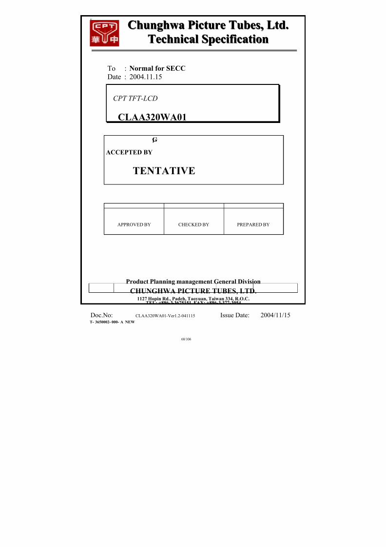
8/18/2019 Akai Lcd Tv Lct3201td_service Masnual
http://slidepdf.com/reader/full/akai-lcd-tv-lct3201tdservice-masnual 70/108
f
CChhuunngghhwwaa PPiiccttuurree TTuubbeess,, LLttdd..
TTeecchhnniiccaall SSppeecciif f iiccaattiioonn
To : Normal for SECC
Date : 2004.11.15
ACCEPTED BY¡
TENTATIVE
APPROVED BY CHECKED BY PREPARED BY
Product Planning management General Division
CHUNGHWA PICTURE TUBES, LTD.1127 Hopin Rd., Padeh, Taoyuan, Taiwan 334, R.O.C.
TEL: +886-3-3675151 FAX: +886-3-377-3054
D N I D t 2004/11/15
CPT TFT-LCD
CLAA320WA01
8/18/2019 Akai Lcd Tv Lct3201td_service Masnual
http://slidepdf.com/reader/full/akai-lcd-tv-lct3201tdservice-masnual 71/108
CPT CHUNGHWA PICTURES TUBES, LTD.,
RECORD OF REVISIONS
Revision No. Date Page Description
Ver1.0 2004/10/18 all Preliminary specification was first issued .
Ver1.1 2004/10/25 -- Update
Ver1.2 2004/11/15 -- Update
8/18/2019 Akai Lcd Tv Lct3201td_service Masnual
http://slidepdf.com/reader/full/akai-lcd-tv-lct3201tdservice-masnual 72/108
CPT CHUNGHWA PICTURES TUBES, LTD.,
CONTENTS
No Item Page
1 OVERVIEW 3
2 ABSOLUTE MAXIMUM RATINGS 4
3 ELECTRICAL CHARACTERISTICS 5
4 INTERFACE PIN CONNECTION 10
5 INTERFACE TIMING 13
6 BLOCK DIAGRAM 18
7 MECHANICAL SPECIFICATION 19
8 OPTICAL CHARACTERISTICS 21
9 RELIABILITY TEST CONDITIONS 26
10 PACKAGING 27
11 DEFINITION OF LABELS 29
12 HANDLING PRECAUTIONS FOR TFT-LCD MODULE 31
8/18/2019 Akai Lcd Tv Lct3201td_service Masnual
http://slidepdf.com/reader/full/akai-lcd-tv-lct3201tdservice-masnual 73/108
CPT CHUNGHWA PICTURES TUBES, LTD.,
1. OVERVIEW
CLAA320WA01 is 32” color (80.04cm) TFT-LCD (Thin Film Transistor Liquid Crystal Display)
module composed of LCD panel, LVDS driver ICs, control circuit and backlight. By applying 8 bit
digital data, 1366*768, 16.7 million-color images are displayed on the 32” diagonal screen. Interface of
data and control signals is Typ. Inverter for backlight is included in this module. General specification
are summarized in the following table:
1.1GENERAL INFORMATION
Items Specifications Unit
Display Area 697.68(H) × 392.25(V) (31.51 inch diagonal) mm
Number of Pixels 1366(H) × 768(V) 16:9
Pixel Pitch 0.51075(H) × 0.51075(V) mm
Color Pixel Arrangement RGB Vertical Strip
Display Mode Normally Black
Number of Colors 16.7M (8bits) color
Surface TreatmentHard coating : 3H ,
Anti-reflective coating <less than 2% reflection.
Total Module Power 115 W
1.2 MECHANICAL INFORMATION
Items Min Typ. Max. Unit
Horizontal(H) 742.0 743.0 744.0 mm
Vertical(V) 446.0 447.0 448.0 mm
without inverter 41.0 42.0 43.0 mm
Module
outline
dimension Depth(D)with inverter 43.0 44.0 45.0 mm
Module Weight 7900 8100 8300 g
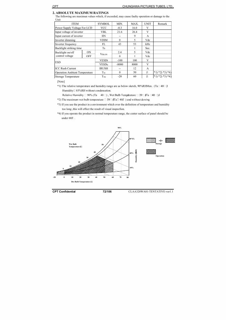
8/18/2019 Akai Lcd Tv Lct3201td_service Masnual
http://slidepdf.com/reader/full/akai-lcd-tv-lct3201tdservice-masnual 74/108
CPT CHUNGHWA PICTURES TUBES, LTD.,
2. ABSOLUTE MAXIMUM RATINGSThe following are maximun values which, if exceeded, may cause faulty operation or damage to the
Unit
ITEM SYMBOL MIN. MAX. UNIT Remark
Power Supply Voltage For LCD VCC -0.3 16.0 V
Input voltage of inverter VBL 21.6 26.4 V
Input current of inverter IIN -- 9 A
Inverter dimming VDIM 0 5 Vdc
Inverter frequency FL 43 53 kHz
Backlight striking time Ts 1 Sec.
ON 2.4 5 VdcBacklight on/off
control voltage OFFVBLON
0 1 Vdc
VESDt -100 100 VESD
VESDc -8000 8000 V
ICC Rush Current IRUSH -- 12 A
Operation Ambient Temperature Top 0 50 ¢J *1) *2) *3) *4)
Storage Temperature Tstg -20 60 ¢J *1) *2) *3) *4)
[Note]
*1) The relative temperature and humidity range are as below sketch, 90%RHMax. (Ta 40 )¡ Ø ¢ J
Humidity 85%RH without condensation.¡Ø
Relative Humidity 90% (Ta 40 )¡ Ø ¡ Ø ¢ J, Wet Bulb Temperature 39 (Ta 40 )¡ Ø ¢ J ¡ Ù ¢ J
*2) The maximum wet bulb temperature 39 (Ta¡ Ø ¢ J ¡Ö 40 ) and without dewing.¢J
*3) If you use the product in a environment which over the definition of temperature and humidity
too long ,this will effect the result of visual inspecfion.
*4) If you operate the product in normal temperature range, the center surface of panel should be
under 60 .¢J
90%
10 20 30 40 50 60 70 800-20
0
10
20
30
40
50
Dry Bulb Temperature [C]
Wet Bulb
Temperature [C]
Storage
Operation
H u m i d i t y [ ( % ) R H ]
10%
40%
60%%
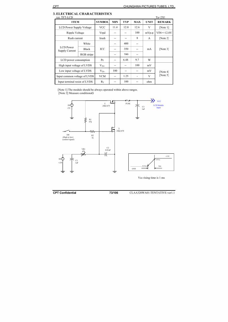
8/18/2019 Akai Lcd Tv Lct3201td_service Masnual
http://slidepdf.com/reader/full/akai-lcd-tv-lct3201tdservice-masnual 75/108
CPT CHUNGHWA PICTURES TUBES, LTD.,
3. ELECTRICAL CHARACTERISTICS(a). TFT-LCD Ta=25¢J
ITEM SYMBOL MIN TYP MAX UNIT REMARK
LCD Power Supply Voltage VCC 11.4 12.0 12.6 V [Note 1]
Ripple Voltage Vrpd -- -- 100 mVp-p VIN=+12.0V
Rush current Irush -- -- 8 A [Note 2]
White -- 400 --
Black -- 350 --LCD Power
Supply Current
RGB stripe
ICC
-- 390 --
mA [Note 3]
LCD power consumption Pc -- 6.48 9.7 W
High input voltage of LVDS VIN+ -- -- 100 mV
Low input voltage of LVDS VIN- 100 -- -- mV
Input common voltage of LVDS VCM -- 1.25 - V
Input terminal resist of LVDS R T -- 100 -- ohm
[Note 4][Note 5]
[Note 1] The module should be always operated within above ranges.
[Note 2] Measure conditions¡G
DC
DC
+5V
R1
47k
R2
1k
VR1
47k
C1
1uF
C2
0.01uF
Q1
2SK1475 C31uF
FUSE
+15V
SW
(High to low)
(control signal)
Q2
2SK1470
VCC
LCD Module
Input
Vcc rising time is 1 ms
1ms
GND
+12V
0.1Vcc
0.9Vcc
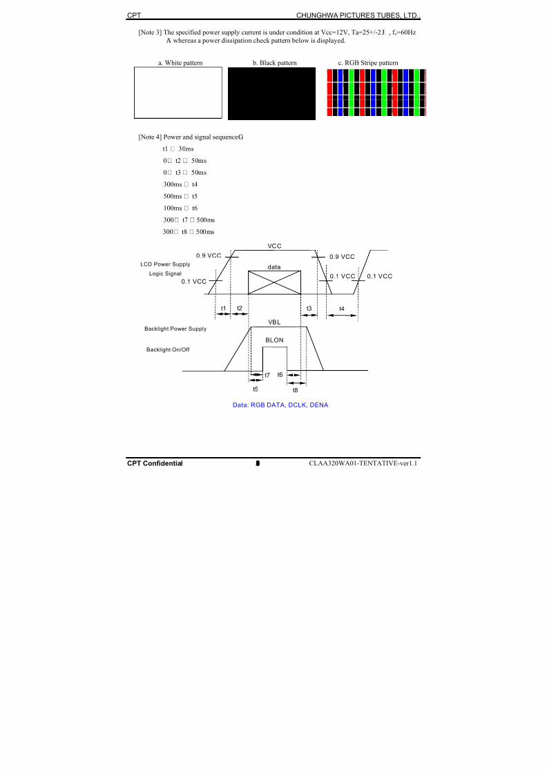
8/18/2019 Akai Lcd Tv Lct3201td_service Masnual
http://slidepdf.com/reader/full/akai-lcd-tv-lct3201tdservice-masnual 76/108
CPT CHUNGHWA PICTURES TUBES, LTD.,
[Note 3] The specified power supply current is under condition at Vcc=12V, Ta=25+/-2¢J , f v=60Hz
¡A whereas a power dissipation check pattern below is displayed.
a. White pattern b. Black pattern c. RGB Stripe pattern
[Note 4] Power and signal sequence¡G
t1 ¡Ø 30ms
0¡Õ t2 ¡Õ 50ms
0¡Õ t3 ¡Ø 50ms
300ms ¡Ø t4
500ms ¡Ø t5
100ms ¡Ø t6
300¡Õ t7 ¡Ø 500ms
300¡Õ t8 ¡Ø 500ms
t1 t2 t3
data
0.9 VCC0.9 VCC
0.1 VCC
VCC
0.1 VCC 0.1 VCC
t4
LCD Power Supply
Logic Signal
t5
t6
Backlight On/OffBLON
Data: RGB DATA, DCLK, DENA
Backlight Power SupplyVBL
t7
t8
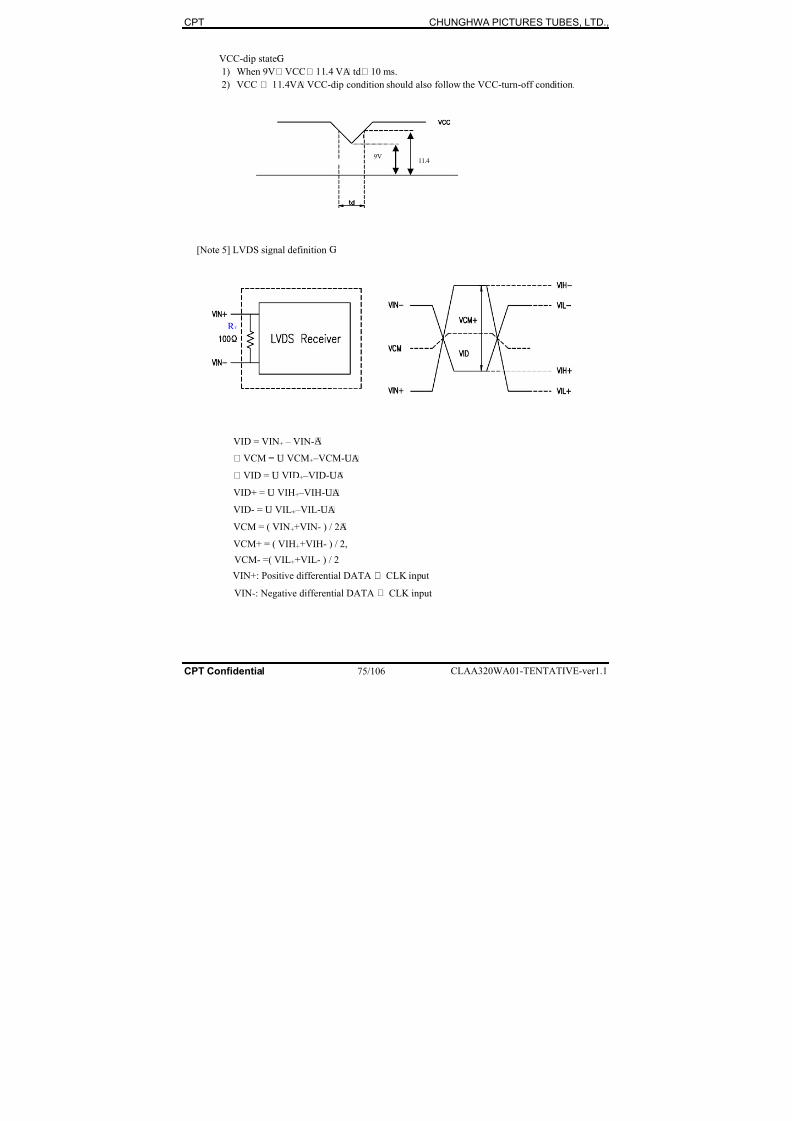
8/18/2019 Akai Lcd Tv Lct3201td_service Masnual
http://slidepdf.com/reader/full/akai-lcd-tv-lct3201tdservice-masnual 77/108
CPT CHUNGHWA PICTURES TUBES, LTD.,
VCC-dip state¡G
1) When 9V VCC¡Ø ¡Õ 11.4 V¡A td 10 ms.¡Ø
2) VCC ¡Ö 11.4V¡A VCC-dip condition should also follow the VCC-turn-off condition.
[Note 5] LVDS signal definition ¡G
VID = VIN+ – VIN-¡A
VCM =¡µ ¡U VCM+ –VCM-¡U¡A
VID =¡µ ¡U VID+ –VID-¡U¡A
VID+ = ¡U VIH+ –VIH-¡U¡AVID- = ¡U VIL+ –VIL-¡U¡A
VCM = ( VIN++VIN- ) / 2¡A
VCM+ = ( VIH++VIH- ) / 2,
VCM- =( VIL++VIL- ) / 2
VIN+: Positive differential DATA ¡® CLK input
VIN-: Negative differential DATA ¡® CLK input
9V11.4
R T

8/18/2019 Akai Lcd Tv Lct3201td_service Masnual
http://slidepdf.com/reader/full/akai-lcd-tv-lct3201tdservice-masnual 78/108
CPT CHUNGHWA PICTURES TUBES, LTD.,
(b). Backlight
Ta=25¢J
ITEM SYMBOL MIN TYP MAX UNIT REMARK
Lamp Voltage VL -- 1150 -- Vrms IL=5.0mA
Lamp Current IL 4.7 5.0 5.3 mArms [Note 1]
Lamp life time LT 50,000 60,000 -- hr [Note 2]
Input voltage of inverter VBL 21.6 24 26.4 V
Input current of inverter IIN 0 4.3 5 A[Note 3]
Input frequency of inverter FL 43 48 53 KHz [Note 4]
Inverter dimming VDIM 0 -- 5 Vdc [Note 5]
Inverter duty ratio -- 30 -- 100 % VDIM=5V(MAX.)
Inverter opening voltage Vopen 2300 -- 2700 Vrms
ON 2.4 -- 5Backlight on /of
control voltage OFFVBLON
0 -- 1V [Note 6]
Power consumption
(Panel+ Backlight )BLW -- 105 115 W After starting 30 mins
Ta=0¢J 2300 -- 3000Start up
Voltage Ta=25¢J
Vs
1960 -- 3000
Vrms
[Note]*1) Lamp Current measurement method (The current meter is connected to low voltage end)
Take the average of 16 CCFL’s lamp current as VDIM = 5V .

8/18/2019 Akai Lcd Tv Lct3201td_service Masnual
http://slidepdf.com/reader/full/akai-lcd-tv-lct3201tdservice-masnual 79/108
CPT CHUNGHWA PICTURES TUBES, LTD.,
*2) Definition of the lamp life time¡G
When lamp luminance redue to 50% or lower than its initial value.
*3) Ripple voltage that occars at the instant of power-on can’t exceed 30V.
*4) Electrical and optical characterisitics color chromaticity is not included can maintain in a range
+/- 10% when the inverter operates within this frequency range.
*5) Brightness is the darkest when VDIM = 0V ; Brightness is the darkest when VDIM = 5V .
*6) Backlight turns off when VBLON = 0V ; turns on when VBLON = 5V(24V must be input in advance)
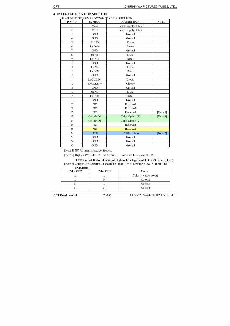
8/18/2019 Akai Lcd Tv Lct3201td_service Masnual
http://slidepdf.com/reader/full/akai-lcd-tv-lct3201tdservice-masnual 80/108
CPT CHUNGHWA PICTURES TUBES, LTD.,
4. INTERFACE PIN CONNECTION(a).Connector Part No.¡G FI-X30SSL-HF(JAE) or compatible
PIN NO SYMBOL DESCRIPTION NOTE
1 VCC Power supply: +12V
2 VCC Power supply: +12V
3 GND Ground
4 GND Ground
5 RxIN0- Data-
6 RxIN0+ Data+
7 GND Ground
8 RxIN1- Data-
9 RxIN1+ Data+
10 GND Ground
11 RxIN2- Data-
12 RxIN2+ Data+13 GND Ground
14 RxCLKIN- Clock-
15 RxCLKIN+ Clock+
16 GND Ground
17 RxIN3- Data-
18 RxIN3+ Data+
19 GND Ground
20 NC Reserved
21 NC Reserved22 NC Reserved [Note 1]
23 ColorMD1 Color Option (1) [Note 3]
24 ColorMD2 Color Option (2)
25 NC Reserved
26 NC Reserved
27 DMS LVDS Option [Note 2]
28 GND Ground
29 GND Ground
30 GND Ground
[Note 1] NC for internal use. Let it open.
[Note 2] High (3.3V) →JEIDA LVDS format¡F Low (GND) → None-JEIDA
LVDS format,It should be input High or Low logic level¡ it can’t be NC(Open).
[Note 3] Color matrix selection. It should be input High or Low logic level¡A it can’t be
NC(Open).
ColorMD2 ColorMD1 Mode
L L Color 1(Native color)
L H Color 2H L Color 3
H H C l 4
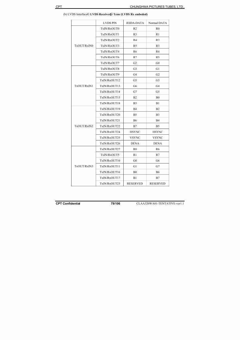
8/18/2019 Akai Lcd Tv Lct3201td_service Masnual
http://slidepdf.com/reader/full/akai-lcd-tv-lct3201tdservice-masnual 81/108
CPT CHUNGHWA PICTURES TUBES, LTD.,
(b) LVDS Interface¡G LVDS Receiver¡ Tcon (LVDS Rx embeded)
LVDS PIN JEIDA-DATA Normal DATA
TxIN/RxOUT0 R2 R0
TxIN/RxOUT1 R3 R1
TxIN/RxOUT2 R4 R2
TxIN/RxOUT3 R5 R3
TxIN/RxOUT4 R6 R4
TxIN/RxOUT6 R7 R5
TxOUT/RxIN0
TxIN/RxOUT7 G2 G0
TxIN/RxOUT8 G3 G1
TxIN/RxOUT9 G4 G2
TxIN/RxOUT12 G5 G3
TxIN/RxOUT13 G6 G4
TxIN/RxOUT14 G7 G5
TxIN/RxOUT15 B2 B0
TxOUT/RxIN1
TxIN/RxOUT18 B3 B1
TxIN/RxOUT19 B4 B2
TxIN/RxOUT20 B5 B3
TxIN/RxOUT21 B6 B4
TxIN/RxOUT22 B7 B5
TxIN/RxOUT24 HSYNC HSYNC
TxIN/RxOUT25 VSYNC VSYNC
TxOUT/RxIN2
TxIN/RxOUT26 DENA DENA
TxIN/RxOUT27 R0 R6TxIN/RxOUT5 R1 R7
TxIN/RxOUT10 G0 G6
TxIN/RxOUT11 G1 G7
TxIN/RxOUT16 B0 B6
TxIN/RxOUT17 B1 B7
TxOUT/RxIN3
TxIN/RxOUT23 RESERVED RESERVED
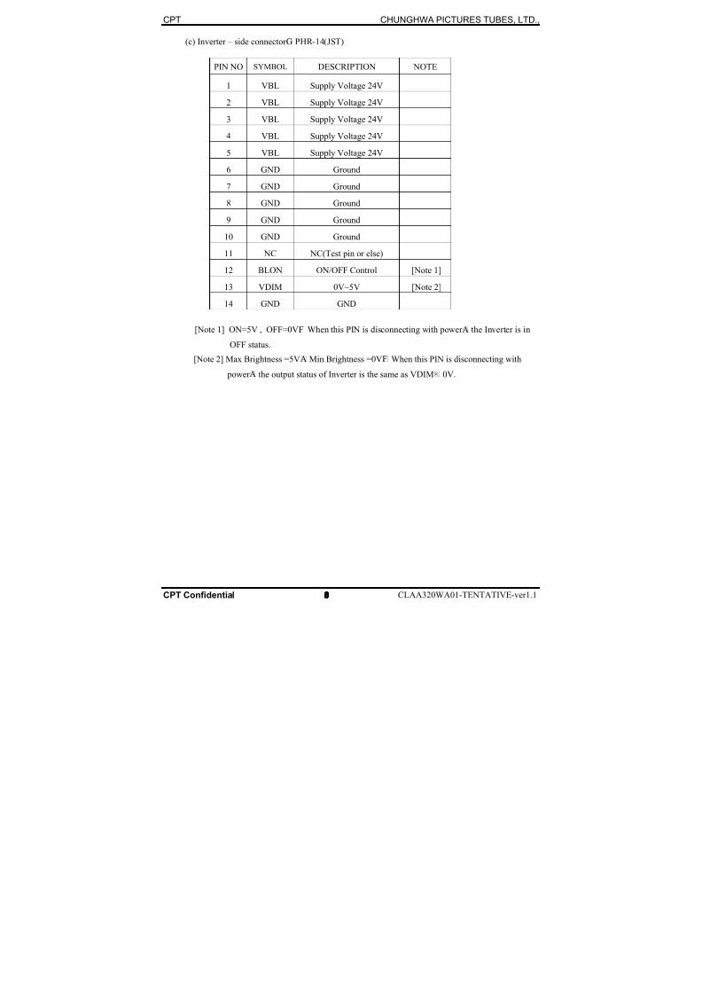
8/18/2019 Akai Lcd Tv Lct3201td_service Masnual
http://slidepdf.com/reader/full/akai-lcd-tv-lct3201tdservice-masnual 82/108
CPT CHUNGHWA PICTURES TUBES, LTD.,
(c) Inverter – side connector¡G PHR-14(JST)
PIN NO SYMBOL DESCRIPTION NOTE
1 VBL Supply Voltage 24V
2 VBL Supply Voltage 24V
3 VBL Supply Voltage 24V
4 VBL Supply Voltage 24V
5 VBL Supply Voltage 24V
6 GND Ground
7 GND Ground
8 GND Ground
9 GND Ground
10 GND Ground
11 NC NC(Test pin or else)
12 BLON ON/OFF Control [Note 1]
13 VDIM 0V~5V [Note 2]
14 GND GND
[Note 1] ON=5V , OFF=0V¡F When this PIN is disconnecting with power¡A the Inverter is in
OFF status.
[Note 2] Max Brightness =5V¡A Min Brightness =0V¡F When this PIN is disconnecting with
power ¡A the output status of Inverter is the same as VDIM¡× 0V.
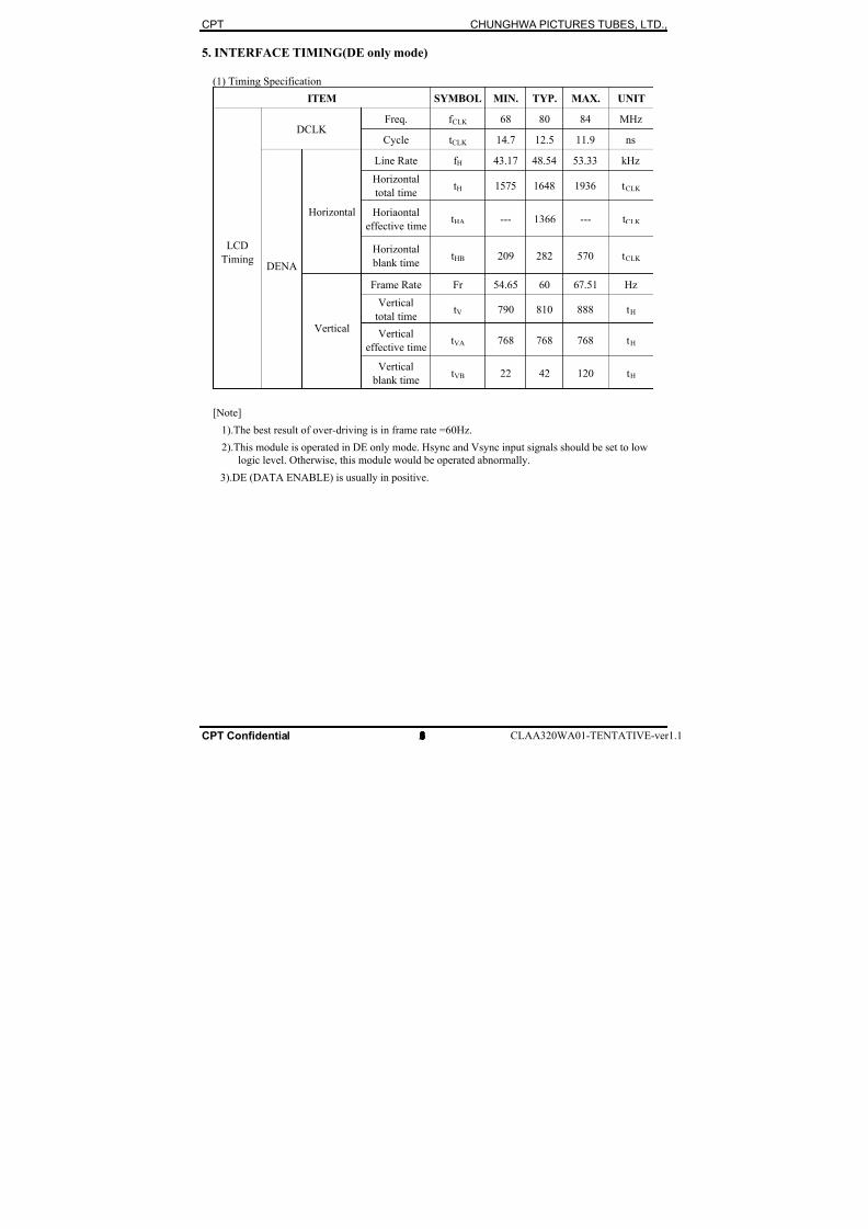
8/18/2019 Akai Lcd Tv Lct3201td_service Masnual
http://slidepdf.com/reader/full/akai-lcd-tv-lct3201tdservice-masnual 83/108
CPT CHUNGHWA PICTURES TUBES, LTD.,
5. INTERFACE TIMING(DE only mode)
(1) Timing Specification
ITEM SYMBOL MIN. TYP. MAX. UNIT
Freq. f CLK 68 80 84 MHzDCLK
Cycle tCLK 14.7 12.5 11.9 ns
Line Rate f H 43.17 48.54 53.33 kHz
Horizontal
total timetH 1575 1648 1936 tCLK
Horiaontal
effective timetHA --- 1366 --- tCLK
Horizontal
Horizontal
blank timetHB 209 282 570 tCLK
Frame Rate Fr 54.65 60 67.51 Hz
Vertical
total timetV 790 810 888 tH
Vertical
effective timetVA 768 768 768 tH
LCD
Timing
DENA
Vertical
Vertical
blank timetVB 22 42 120 tH
[Note]
1).The best result of over-driving is in frame rate =60Hz.
2).This module is operated in DE only mode. Hsync and Vsync input signals should be set to low
logic level. Otherwise, this module would be operated abnormally.
3).DE (DATA ENABLE) is usually in positive.
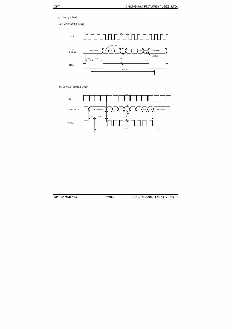
8/18/2019 Akai Lcd Tv Lct3201td_service Masnual
http://slidepdf.com/reader/full/akai-lcd-tv-lct3201tdservice-masnual 84/108
CPT CHUNGHWA PICTURES TUBES, LTD.,
(2) Timing Chart
a. Horizontal Timing
DCLK
DATA (R,G,B)
1 2 1365 1366 3 Invalid Data Invalid Data
tHA tHFP t HBP
tH=1/f H
First Data
Last Data
DENA
1 2 767 768 3Invalid Data Invalid Data
t VFP t VBP
tV=1/f V
LINE DATA
DENA
HD
tVA
b. Vertical Timing Chart
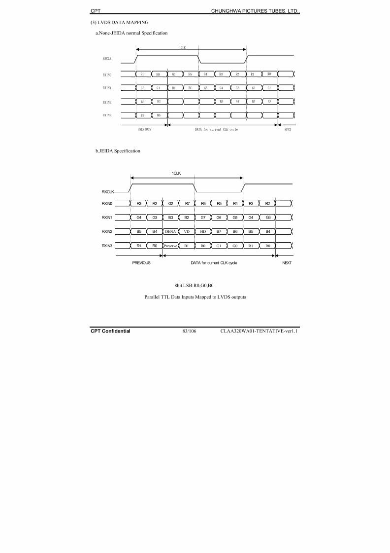
8/18/2019 Akai Lcd Tv Lct3201td_service Masnual
http://slidepdf.com/reader/full/akai-lcd-tv-lct3201tdservice-masnual 85/108
CPT CHUNGHWA PICTURES TUBES, LTD.,
(3) LVDS DATA MAPPING
a.None-JEIDA normal Specification
b.JEIDA Specification
8bit LSB:R0,G0,B0
Parallel TTL Data Inputs Mapped to LVDS outputs
B2 B3 B3 B4 B5 B2
R1 R0 R4 R5 G0 R2 R3 R1 R0
G2 G1 B1 B0 G4 G5 G3 G2 G1
RXCLK
RXIN0
RXIN1
RXIN2
1CLK
DATA for current CLK cycle NEXT
RXIN3 R6 R7
PREVIOUS
B4 DENAB5 B5B6B7 B4
R3 R2 R6R7G2 R4R5 R3 R2
G4 G3 B3 B2 G6G7 G5 G4
RXCLK
RXIN1
RXIN2
1CLK
DATA for current CLK cycle NEXT
RXIN3 R0 Preserve B1 B0R1 R1G0G1 R0
PREVIOUS
VD HD
RXIN0
G3
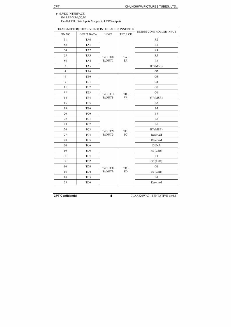
8/18/2019 Akai Lcd Tv Lct3201td_service Masnual
http://slidepdf.com/reader/full/akai-lcd-tv-lct3201tdservice-masnual 86/108
CPT CHUNGHWA PICTURES TUBES, LTD.,
(4) LVDS INTERFACE
8bit LSB¡G R0,G0,B0
Parallel TTL Data Inputs Mapped to LVDS outputs
TRANSMITTER(THC63LVD823) INTERFACE CONNECTOR
PIN NO INPUT DATA HOST TFT_LCDTIMING CONTROLLER INPUT
51 TA0 R2
52 TA1 R3
54 TA2 R4
55 TA3 R5
56 TA4 R6
3 TA5 R7 (MSB)
4 TA6
TxOUT0+
TxOUT0-
TA+
TA-
G26 TB0 G3
7 TB1 G4
11 TB2 G5
12 TB3 G6
14 TB4 G7 (MSB)
15 TB5 B2
19 TB6
TxOUT1+
TxOUT1-
TB+
TB-
B3
20 TC0 B4
22 TC1 B5
23 TC2 B6
24 TC3 B7 (MSB)
27 TC4 Reserved
28 TC5 Reserved
30 TC6
TxOUT2+
TxOUT2-
TC+
TC-
DENA
50 TD0 R0 (LSB)
2 TD1 R1
8 TD2 G0 (LSB)
10 TD3 G1
16 TD4 B0 (LSB)
18 TD5 B1
25 TD6
TxOUT3+
TxOUT3-
TD+
TD-
Reserved
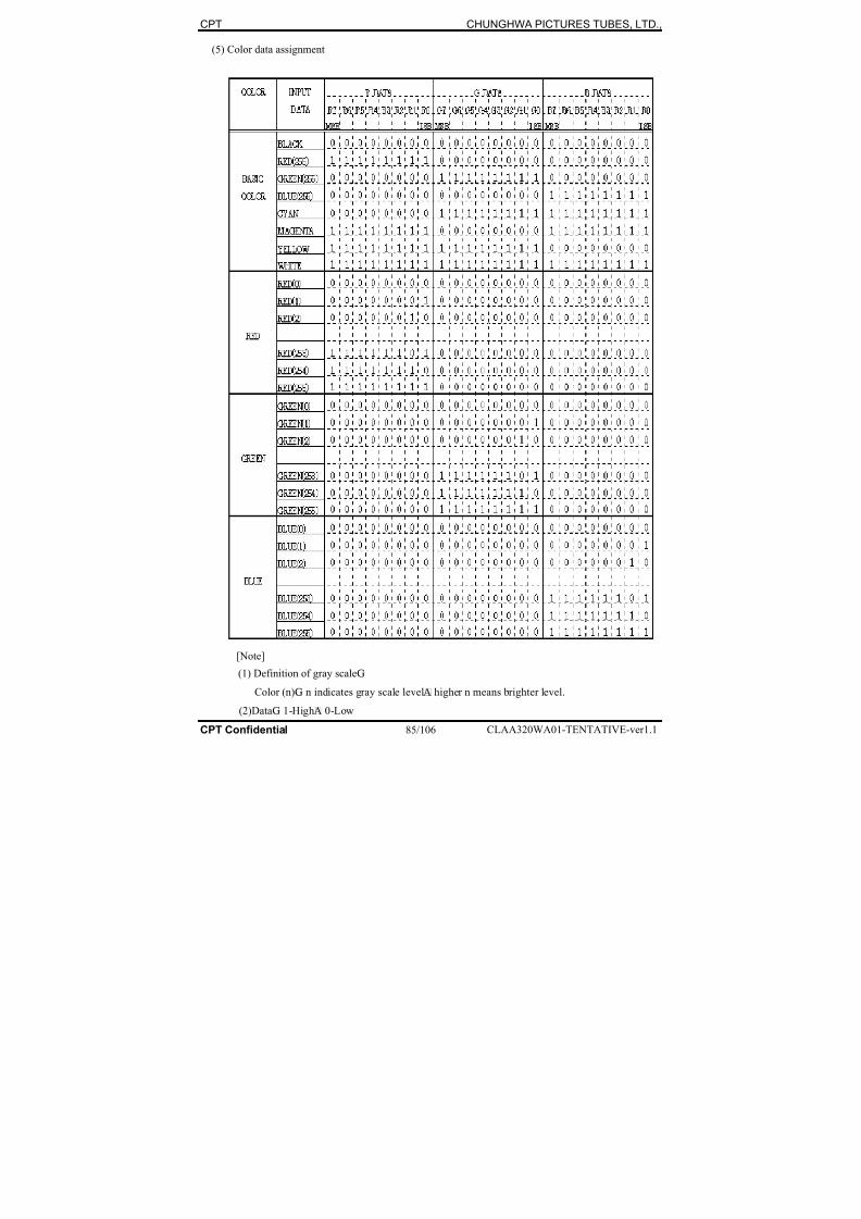
8/18/2019 Akai Lcd Tv Lct3201td_service Masnual
http://slidepdf.com/reader/full/akai-lcd-tv-lct3201tdservice-masnual 87/108
CPT CHUNGHWA PICTURES TUBES, LTD.,
(5) Color data assignment
[Note]
(1) Definition of gray scale¡G
Color (n)¡G n indicates gray scale level¡A higher n means brighter level.
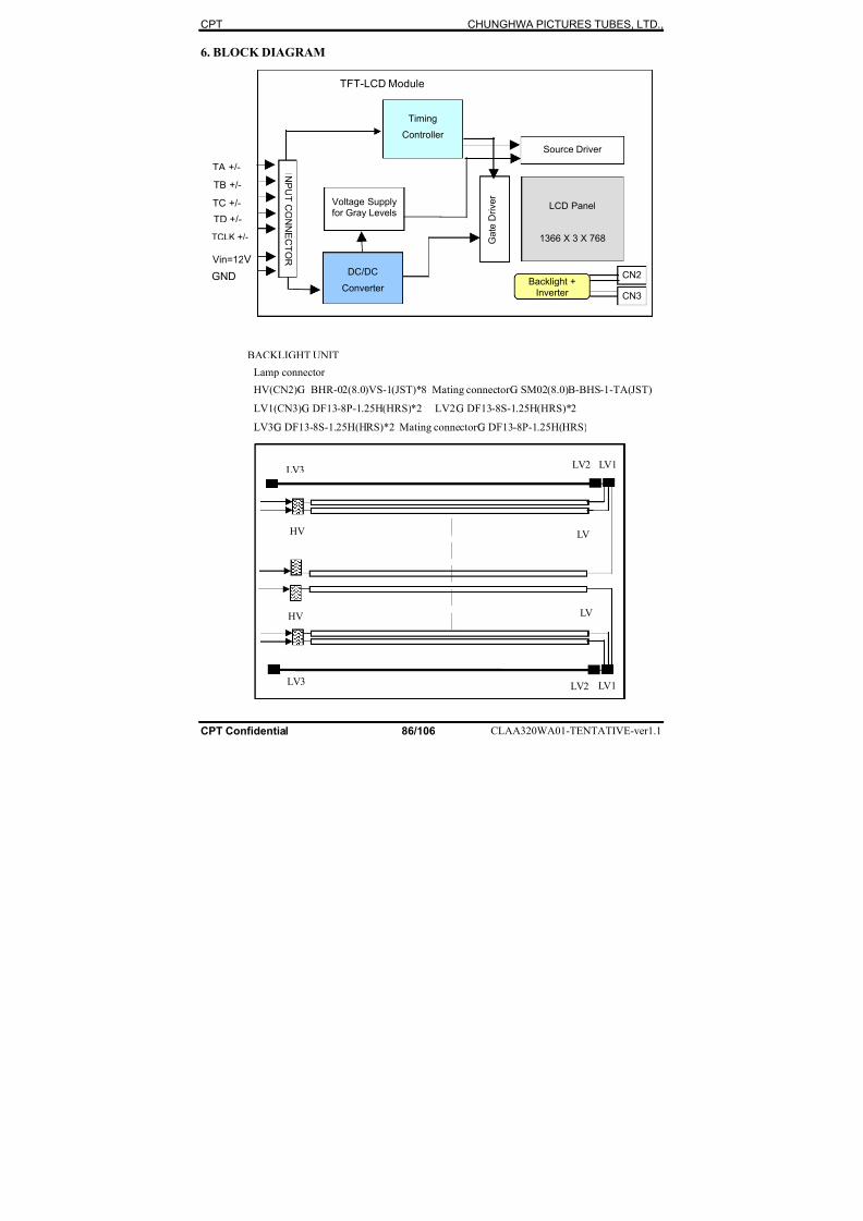
8/18/2019 Akai Lcd Tv Lct3201td_service Masnual
http://slidepdf.com/reader/full/akai-lcd-tv-lct3201tdservice-masnual 88/108
CPT CHUNGHWA PICTURES TUBES, LTD.,
6. BLOCK DIAGRAM
CN2
CN3
Backlight +Inverter
I NP UT C ONNE C T OR
Timing
Controller
G a t e D r i v e r
Voltage Supplyfor Gray Levels
DC/DC
Converter
TFT-LCD Module
Source Driver
LCD Panel
1366 X 3 X 768
TA +/-
TB +/-
TC +/-
TD +/-
TCLK +/-
Vin=12V
GND
BACKLIGHT UNIT
Lamp connector
HV(CN2)¡G BHR-02(8.0)VS-1(JST)*8 Mating connector¡G SM02(8.0)B-BHS-1-TA(JST)
LV1(CN3)¡G DF13-8P-1.25H(HRS)*2 LV2¡G DF13-8S-1.25H(HRS)*2
LV3¡G DF13-8S-1.25H(HRS)*2 Mating connector¡G DF13-8P-1.25H(HRS)
LV2LV3
LV1
HV
LV3
LV1
LV2
HV
LV
LV
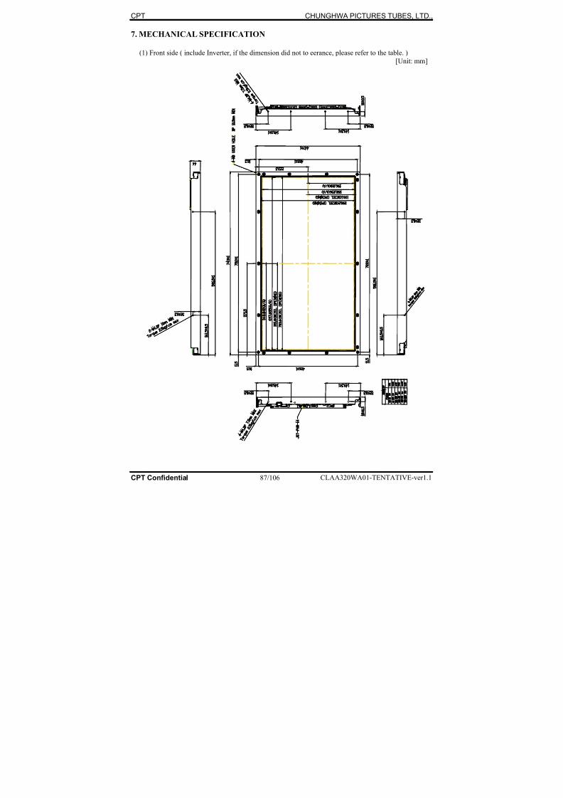
8/18/2019 Akai Lcd Tv Lct3201td_service Masnual
http://slidepdf.com/reader/full/akai-lcd-tv-lct3201tdservice-masnual 89/108
CPT CHUNGHWA PICTURES TUBES, LTD.,
7. MECHANICAL SPECIFICATION
(1) Front side ( include Inverter, if the dimension did not to eerance, please refer to the table. )
[Unit: mm]
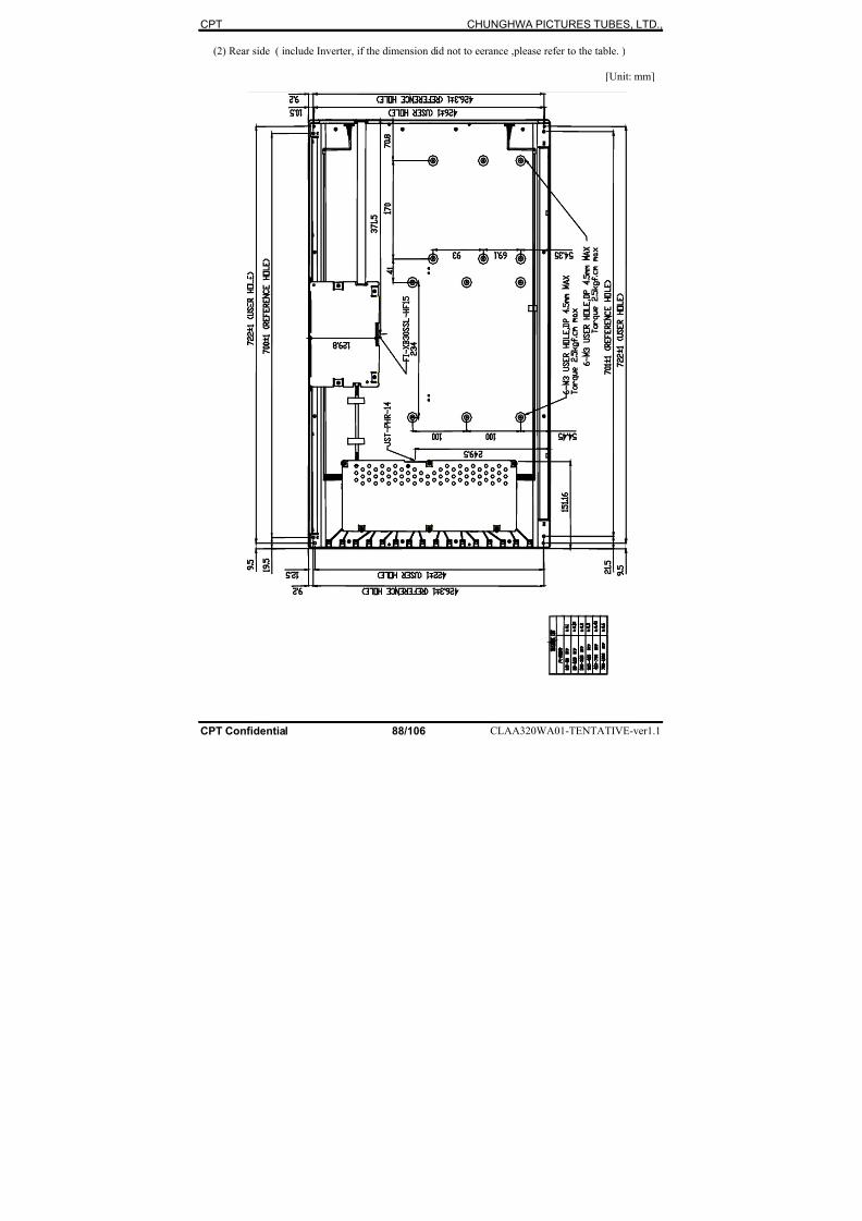
8/18/2019 Akai Lcd Tv Lct3201td_service Masnual
http://slidepdf.com/reader/full/akai-lcd-tv-lct3201tdservice-masnual 90/108
CPT CHUNGHWA PICTURES TUBES, LTD.,
(2) Rear side ( include Inverter, if the dimension did not to eerance ,please refer to the table. )
[Unit: mm]
8/18/2019 Akai Lcd Tv Lct3201td_service Masnual
http://slidepdf.com/reader/full/akai-lcd-tv-lct3201tdservice-masnual 91/108
CPT CHUNGHWA PICTURES TUBES, LTD.,
8.OPTICAL CHARACTERISTICSTa = 25°C, VCC=5V
ITEM SYMBOL CONDITION MIN. TYP. MAX. UNIT REMARKS
Contrast (CEN) CRθ=ψ 0°
Point-5600 800 -- -- *1)*2)*3)
Central
luminance Lwc θ=ψ 0° 500 550 -- cd/m2
9P Luminance
(AVG)Lw9 θ=ψ 0° -- 500 -- cd/m2 *2)*3)Luminance
Uniformity ¡µ Lw θ=ψ 0° -- -- 75 % *2)*3)
Contrast Uniformity ¡µ CR θ=ψ 0° -- -- 75 % *1)*2)*3)
tr θ=ψ 0° -- 7 15 ms *3)*4)Response Time
( White – Black ) tf θ=ψ 0° 9 15 ms *3)*4)
Response Time
(Gray to gray average) trg, tfg ¡@ -- 10 TBD ms *5)
2 h -- -- 5 sec *6)Image sticking tis
24 h -- -- < 16 sec *6)
Horizontal ψ -80~80 -85~85 -- ° *2)*3)View angle
Vertical θ
CR ¡Ù 10
Point-5 -80~80 -85~85 -- ° *2)*3)
Crosstalk Ratio CMR θ=ψ 0° -- -- 1 % *3)*7)
Red
Rx
Ry
0.610
0.295
0.640
0.325
0.670
0.355
GreenGx
Gy
0.235
0.596
0.265
0.626
0.295
0.656
BlueBx
By
0.115
0.031
0.145
0.061
0.175
0.091
Color
Chromaticity
WhiteWx
Wy
θ=ψ 0°
Point-5
0.253
0.267
0.283
0.297
0.313
0.327
-- *2)*3)
Color Temperature Tc -- 9300 -- K *3)
Color Gamut CG -- 72 -- % *8)
[Note]
These items are measured using¡G BM-5A (TOPCON) [ under the dark room condition (no ambient
light). ]
Measurement Condition¡G
After lighting on the panel 30 mins, you can proceed the Measurement testing.
The definiton of Typ ualue is under status of lamp current = 5 mArms.(AVG)
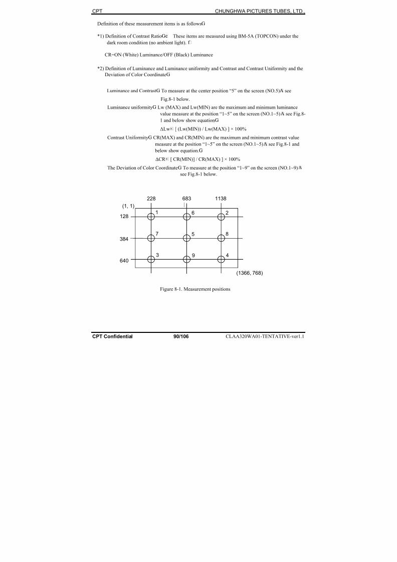
8/18/2019 Akai Lcd Tv Lct3201td_service Masnual
http://slidepdf.com/reader/full/akai-lcd-tv-lct3201tdservice-masnual 92/108
CPT CHUNGHWA PICTURES TUBES, LTD.,
Definition of these measurement items is as follows¡G
*1) Definition of Contrast Ratio¡G¡e These items are measured using BM-5A (TOPCON) under the
dark room condition (no ambient light). ¡f
CR=ON (White) Luminance/OFF (Black) Luminance
*2) Definition of Luminance and Luminance uniformity and Contrast and Contrast Uniformity and the
Deviation of Color Coordinate¡G
Luminance and Contrast¡G To measure at the center position “5” on the screen (NO.5)¡A see
Fig.8-1 below.
Luminance uniformity¡G Lw (MAX) and Lw(MIN) are the maximum and minimum luminance
value measure at the position “1~5” on the screen (NO.1~5)¡A see Fig.8-
1 and below show equation¡G
∆Lw¡× [ (Lw(MIN)) / Lw(MAX) ] × 100%
Contrast Uniformity¡G CR(MAX) and CR(MIN) are the maximum and minimum contrast value
measure at the position “1~5” on the screen (NO.1~5)¡A see Fig.8-1 and
below show equation.¡G
∆CR ¡× [ CR(MIN)] / CR(MAX) ] × 100%
The Deviation of Color Coordinate¡G To measure at the position “1~9” on the screen (NO.1~9)¡A
see Fig.8-1 below.
1 6 2
7 5 8
3 9 4
(1, 1)
128
384
640
228 683
」
1138
(1366, 768)
Figure 8-1. Measurement positions
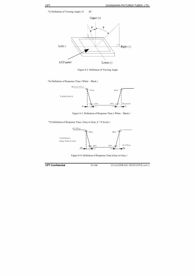
8/18/2019 Akai Lcd Tv Lct3201td_service Masnual
http://slidepdf.com/reader/full/akai-lcd-tv-lct3201tdservice-masnual 93/108
CPT CHUNGHWA PICTURES TUBES, LTD.,
*3) Definition of Viewing Angle ( θ )¡G
Figure 8-2. Definition of Viewing Angle
*4) Definition of Response Time ( White – Black )
L u m i n a n c e
9 0 %9 0 %
1 0 %
t f t r
W h i t e ( 2 5 5 t h )
B l a c k ( 0 )1 0 %
Figure 8-3. Definition of Response Time ( White – Black )
*5) Definition of Response Time ( Gray to Gray ,9 ¡Ñ9 levels )
Luminance
90 %90 %
10 %tfgtrg
(Gray Scale Level)
(0~255 th)
(0~255 th)10 %
Figure 8-4. Definition of Response Time (Gray to Gray )
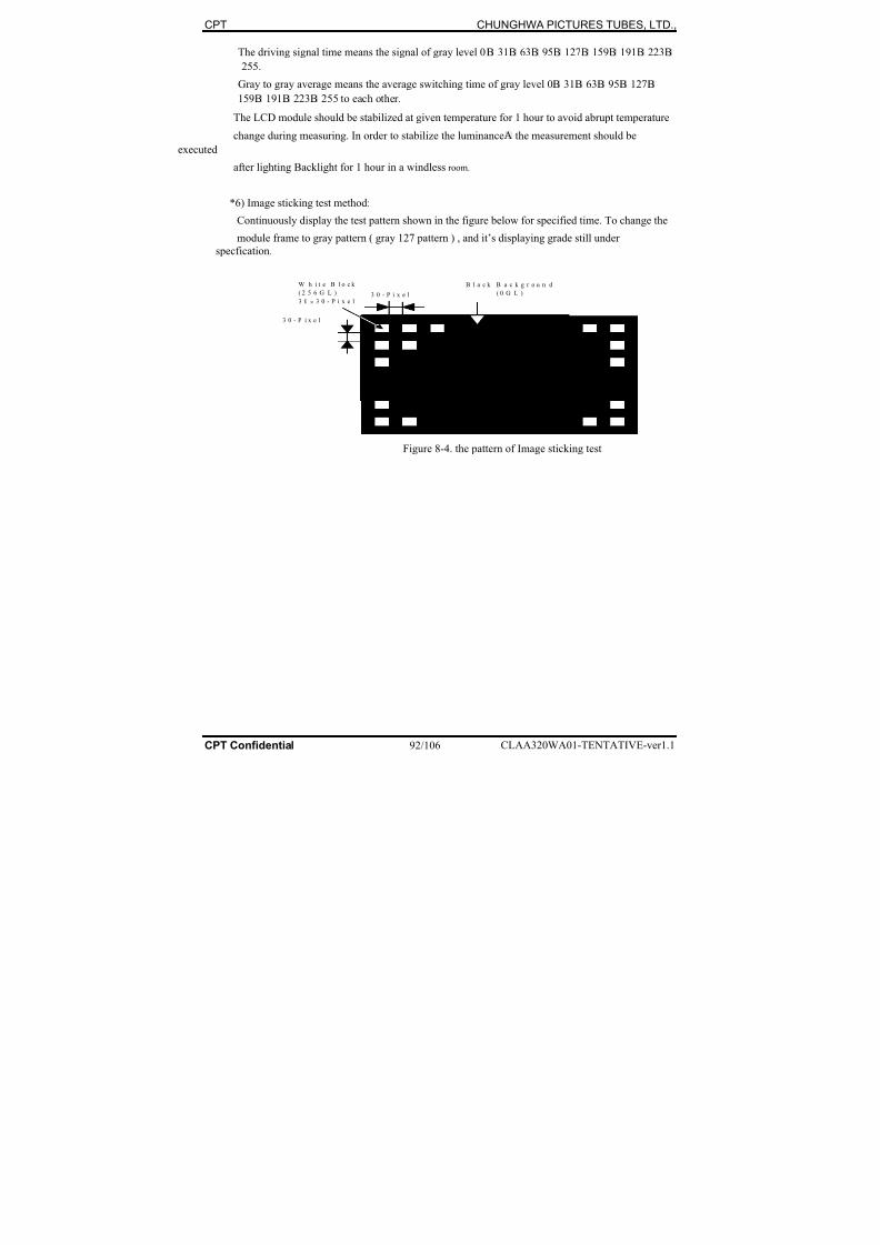
8/18/2019 Akai Lcd Tv Lct3201td_service Masnual
http://slidepdf.com/reader/full/akai-lcd-tv-lct3201tdservice-masnual 94/108
CPT CHUNGHWA PICTURES TUBES, LTD.,
The driving signal time means the signal of gray level 0¡B 31¡B 63¡B 95¡B 127¡B 159¡B 191¡B 223¡B
255.
Gray to gray average means the average switching time of gray level 0¡B 31¡B 63¡B 95¡B 127¡B
159¡B 191¡B 223¡B 255 to each other.
The LCD module should be stabilized at given temperature for 1 hour to avoid abrupt temperature
change during measuring. In order to stabilize the luminance¡A the measurement should bexecuted
after lighting Backlight for 1 hour in a windless room.
*6) Image sticking test method:
Continuously display the test pattern shown in the figure below for specified time. To change the
module frame to gray pattern ( gray 127 pattern ) , and it’s displaying grade still under
specfication.
Figure 8-4. the pattern of Image sticking test
3 0 - P i x e l
・ ・ ・ ・ ・ ・ ・ ・
・ ・ ・ ・ ・ ・ ・ ・ ・ ・ ・ ・
・ ・ ・ ・ ・ ・ ・ ・ ・ ・ ・ ・ ・ ・
・ ・・ ・
・ ・ ・ ・ ・ ・ ・ ・ ・ ・
W h i t e B l o c k
( 2 5 6 G L )
3 0 × 3 0 - P i x e l3 0 - P i x e l
B l a c k B a c k g r o u n d
( 0 G L )
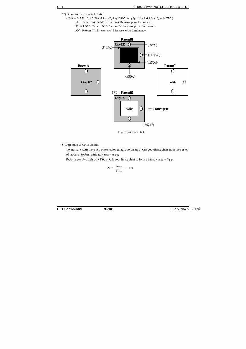
8/18/2019 Akai Lcd Tv Lct3201td_service Masnual
http://slidepdf.com/reader/full/akai-lcd-tv-lct3201tdservice-masnual 95/108
CPT CHUNGHWA PICTURES TUBES, LTD.,
*7) Definition of Cross talk Ratio
CMR = MAX ( ( | ( LB1-LA ) / LC | ) × 100 ( | (LB2 – LA ) / LC | ) × 100 )
LA¡G Pattern A(Half-Tone pattern) Measure point Luminance
LB1¡A LB2¡G Pattern B1¡B Pattern B2 Measure point Luminance
LC¡G Pattern C(white pattern) Measure point Luminance
Figure 8-4. Cross talk
*8) Definition of Color Gamut:
To measure RGB three sub-pixels color gamut coordinate at CIE coordinate chart from the center
of module , to form a triangle area = ARGB.
RGB three sub-pixels of NTSC at CIE coordinate chart to form a triangle area = NRGB.
ARG B
NRG B
CG = × 100
Pattern B1
Gray 127
Black
Pattern A Pattern C
Gray 127 white
Pattern B2
Gray 127
white
(1366,768)
(0,0)
(1024,576)
(341,192)
(1195,384)
(683,96)
(683,672)
measurement point
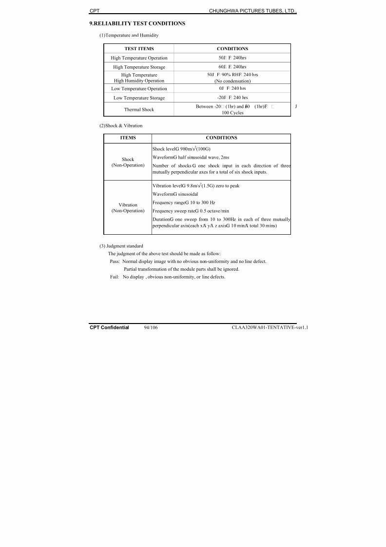
8/18/2019 Akai Lcd Tv Lct3201td_service Masnual
http://slidepdf.com/reader/full/akai-lcd-tv-lct3201tdservice-masnual 96/108
CPT CHUNGHWA PICTURES TUBES, LTD.,
9.RELIABILITY TEST CONDITIONS
(1) Temperature and Humidity
TEST ITEMS CONDITIONS
High Temperature Operation50¢J ¡F 240hrs
High Temperature Storage 60¢J ¡F 240hrs
High Temperature
High Humidity Operation
50¢J ¡F 90% RH¡F 240 hrs
(No condensation)
Low Temperature Operation 0¢J ¡F 240 hrs
Low Temperature Storage -20¢J ¡F 240 hrs
Thermal ShockBetween -20 (1hr) and 60 (1hr)¢ J ¢ J¡F
100 Cycles
(2) Shock & Vibration
ITEMS CONDITIONS
Shock
(Non-Operation)
Shock level¡G 980m/s2(100G)
Waveform¡G half sinusoidal wave, 2ms
Number of shocks ¡G one shock input in each direction of three
mutually perpendicular axes for a total of six shock inputs.
Vibration
(Non-Operation)
Vibration level¡G 9.8m/s2(1.5G) zero to peak
Waveform¡G sinusoidal
Frequency range¡G 10 to 300 Hz
Frequency sweep rate¡G 0.5 octave/min
Duration¡G one sweep from 10 to 300Hz in each of three mutually
perpendicular axis(each x¡A y¡A z axis¡G 10 min¡A total 30 mins)
(3) Judgment standard
The judgment of the above test should be made as follow:
Pass: Normal display image with no obvious non-uniformity and no line defect.
Partial transformation of the module parts shall be ignored.
Fail: No display , obvious non-uniformity, or line defects.
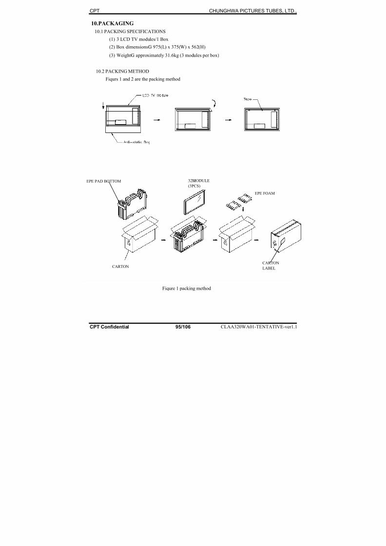
8/18/2019 Akai Lcd Tv Lct3201td_service Masnual
http://slidepdf.com/reader/full/akai-lcd-tv-lct3201tdservice-masnual 97/108
CPT CHUNGHWA PICTURES TUBES, LTD.,
10.PACKAGING
10.1 PACKING SPECIFICATIONS
(1) 3 LCD TV modules/1 Box
(2) Box dimensions¡G 975(L) x 375(W) x 562(H)
(3) Weight¡G approximately 31.6kg (3 modules per box)
10.2 PACKING METHOD
Fiqurs 1 and 2 are the packing method
Fiqure 1 packing method
EPE FOAM
32¡ªMODULE(3PCS)
EPE PAD BOTTOM
CARTONCARTON
LABEL
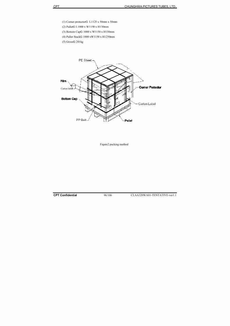
8/18/2019 Akai Lcd Tv Lct3201td_service Masnual
http://slidepdf.com/reader/full/akai-lcd-tv-lct3201tdservice-masnual 98/108
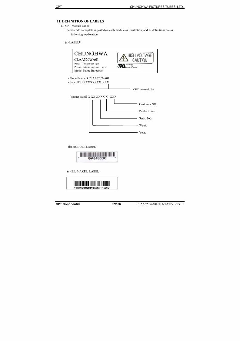
8/18/2019 Akai Lcd Tv Lct3201td_service Masnual
http://slidepdf.com/reader/full/akai-lcd-tv-lct3201tdservice-masnual 99/108
CPT CHUNGHWA PICTURES TUBES, LTD.,
11. DEFINITION OF LABELS
11.1 CPT Module Label
The barcode nameplate is pasted on each module as illustration, and its definitions are as
following explanation.
(a) LABEL¡G
- Model Name¡G CLAA320WA01
- Panel ID¡G XXXXXXXX XXX
CPT Internal Use.
- Product date¡G X XX XXXX X XXX
Customer NO.
Product Line.
Serial NO.
Week.
Year.
(b) MODULE LABEL :
(c) B/L MAKER LABEL :
CHUNGHWA
CLAA32 WA 1
Panel ID:xxxxxxxx xxx
Product date:xxxxxxxxx xxx
Model Name Barecode
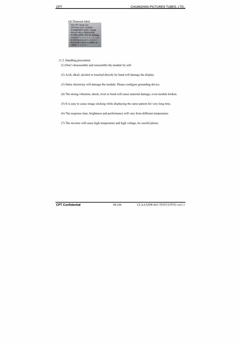
8/18/2019 Akai Lcd Tv Lct3201td_service Masnual
http://slidepdf.com/reader/full/akai-lcd-tv-lct3201tdservice-masnual 100/108
CPT CHUNGHWA PICTURES TUBES, LTD.,
(d) Disposal label
11.2. Handling precaution
(1) Don’t disassemble and reassemble the module by self.
(2) Acid, alkali, alcohol or touched directly by hand will damage the display.
(3) Static electricity will damage the module. Please configure grounding device.
(4) The strong vibration, shock, twist or bend will cause material damage, even module broken.
(5) It is easy to cause image sticking while displaying the same pattern for very long time.
(6) The response time, brightness and performance will vary from different temperature.
(7) The inverter will cause high temperature and high voltage, be careful please.

8/18/2019 Akai Lcd Tv Lct3201td_service Masnual
http://slidepdf.com/reader/full/akai-lcd-tv-lct3201tdservice-masnual 101/108
8/18/2019 Akai Lcd Tv Lct3201td_service Masnual
http://slidepdf.com/reader/full/akai-lcd-tv-lct3201tdservice-masnual 102/108
CPT CHUNGHWA PICTURES TUBES, LTD.,
frames can happen during a long preservation of soiled LCD modules.
(9) Please pay attention to handling lead wire of backlight so that it is not tugged in connecting with
inverter.
12.2 OPERATING PRECAUTIONS
(1) Please be sure to turn off the power supply before connecting and disconnecting signal input
cable.
(2) Please do not change variable resistance settings in LCD module. They are adjusted to the most
suitable value. If they are changed, it might happen LCD does not satisfy the characteristics
specification.
(3) Please consider that LCD backlight takes longer time to become stable of radiation characteristics
in low temperature than in room temperature.
(4) A condensation might happen on the surface and inside of LCD module in case of sudden change
of ambient temperature.
(5) Please pay attention to displaying the same pattern for very long time. Image might stick on LCD.
If then, time going on can make LCD work well.
(6) Please obey the same caution descriptions as ones that need to pay attention to ordinary electronic
parts.
12.3 PRECAUTIONS WITH ELECTROSTATICS
(1) This LCD module use CMOS-IC on circuit board and TFT-LCD panel, and so it is easy to be
affected by electrostatics. Please be careful with electrostatics by the way of your body
connecting to the ground and so on.
(2) Please remove protection film very slowly on the surface of LCD module to prevent from
electrostatics occurrence.
12.4 STORAGE PRECAUTIONS
(1) When you store LCDs for a long time, it is recommended to keep the temperature between 0¢J
~40¢J without the exposure of sunlight and to keep the humidity less than 90%RH.
(2) Please do not leave the LCDs in the environment of high humidity and high temperature such as
60¢J 90%RH
8/18/2019 Akai Lcd Tv Lct3201td_service Masnual
http://slidepdf.com/reader/full/akai-lcd-tv-lct3201tdservice-masnual 103/108
CPT CHUNGHWA PICTURES TUBES, LTD.,
(3) Please do not leave the LCDs in the environment of low temperature; below -20¢J .
12.5 SAFETY PRECAUTIONS
(1) When you waste LCDs, it is recommended to crush damaged or unnecessary LCDs into piecesand wash them off with solvents such as acetone and ethanol, which should later be burned.
(2) If any liquid leaks out of a damaged-glass cell and comes in contact with the hands, wash off
throughly with soap and water.
12.6 OTHERS
(1) A strong incident light into LCD panel might cause display characteristics' changing inferior because of polarizer film, color filter, and other materials becoming inferior. Please do not
expose LCD module direct sunlight Land strong UV rays.
(2) Please pay attention to a panel side of LCD module not to contact with other materials in
preserving it alone.
(3) For the packaging box, please pay attention to the followings:
• Packaging box and inner case for LCD are designed to protect the LCDs from the damage or
scratching during transportation. Please do not open except picking LCDs up from the box.
• Please do not pile them up more than 3 boxes. (They are not designed so.) And please do not
turn over.
• Please handle packaging box with care not to give them sudden shock and vibrations. And
also please do not throw them up.
• Packing box and inner case for LCDs are made of cardboard. So please pay attention not to
get them wet. (Such like keeping them in high humidity or wet place can occur getting them
wet.)
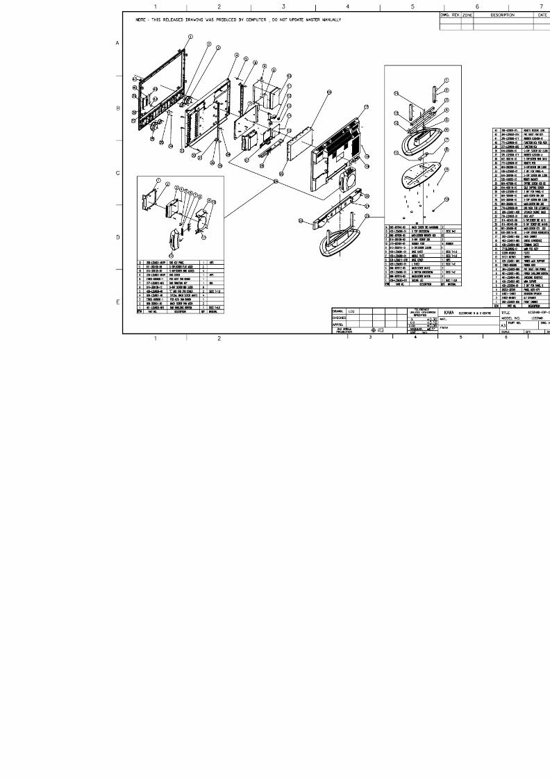
8/18/2019 Akai Lcd Tv Lct3201td_service Masnual
http://slidepdf.com/reader/full/akai-lcd-tv-lct3201tdservice-masnual 104/108
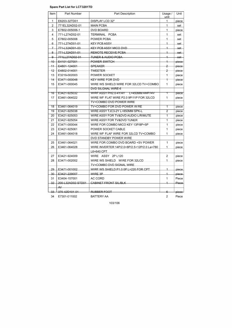
8/18/2019 Akai Lcd Tv Lct3201td_service Masnual
http://slidepdf.com/reader/full/akai-lcd-tv-lct3201tdservice-masnual 105/108
Spare Part List for LCT3201TD
Item Part Number Part Description Usage /unit
Un
1 E6203-32TD01 DISPLAY LCD 32" 1 piec
2 771EL32AD02-01 MAIN PCBA 1 se
3 E7802-005006-1 DVD BOARD 1 piec
4 771-L27AD02-01 TERMINAL PCBA 1 se
5 E7802-005008 POWER PCBA 1 se
6 771-L27AD01-01 KEY PCB ASSY 1 se
7 771-L32AD01-03 KEY PCB ASSY MICO DVD 1 se
8 771-L32AD01-01 REMOTE RECEIVE PCBA 1 se
9 771LL27AD02-01 TUNER & AUDIO PCBA 1 se
10 E4101-027001 POWER SWITCH 1 piec
11 E4801-124001 SPEAKER 2 piec
12 E4802-014001 TWEETER 2 piec
13 E3219-002003 POWER SOCKET 1 piec
14 E3471-000048 KEY WIRE FOR DVD 1 piec
15 E3471-000045 WIRE WS SHIELD WIRE FOR 32LCD TV+COMBO
DVD SILGNAL WIRE-6
1 pie
16 E3421-925032 WIRE ASSY PH2.0-4Y/4Y L=450MM AMP24V 1 piec
17 E3461-064022 WIRE WF FLAT WIRE P2.0 9P/11P FOR 32LCD
TV+COMBO DVD POWER WIRE
1 pie
18 E3461-064019 TV+COMBO FOR DVD POWER WIRE 1 piec
19 E3421-925038 WIRE ASSY TJC3-2Y L=850MM SPK-L 2 piec
20 E3421-925053 WIRE ASSY FOR TV&DVD AUDIO L/R/MUTE 1 piec
21 E3421-925054 WIRE ASSY FOR TV&DVD TUNER 1 piec
22 E3471-000044 WIRE FOR COMBO MICO KEY 13P/8P+5P 1 piec
23 E3421-925061 POWER SOCKET CABLE 1 piec
24 E3461-064018 WIRE WF FLAF WIRE FOR 32LCD TV+COMBO
DVD STANDBY POWER WIRE
1 pie
25 E3461-064021 WIRE FOR COMBO DVD BOARD +SV POWER 1 piec
26 E3461-064028 WIRE INVERTER 14P/2.0+8P/2.5+12P/2.0 La=780
L6=640 CPT
1 pie
27 E3421-924009 WIRE ASSY 2P L120 2 piec
28 E3471-002002 WIRE WS SHIELD WIRE FOR 32LCD
TV+COMBO DVD SIGNAL WIRE
1 pie
29 E3471-001002 WIRE WS SHIELD P1.0 0P L=220 FOR CPT 1 piec
30 E3421-229007 WIRE 3P 1 piec
31 E3404-157001 AC CORD 1 Pie
32 200-L32AD02-STD01
AV
CABINET FRONT SIL/BLK 1 Pie
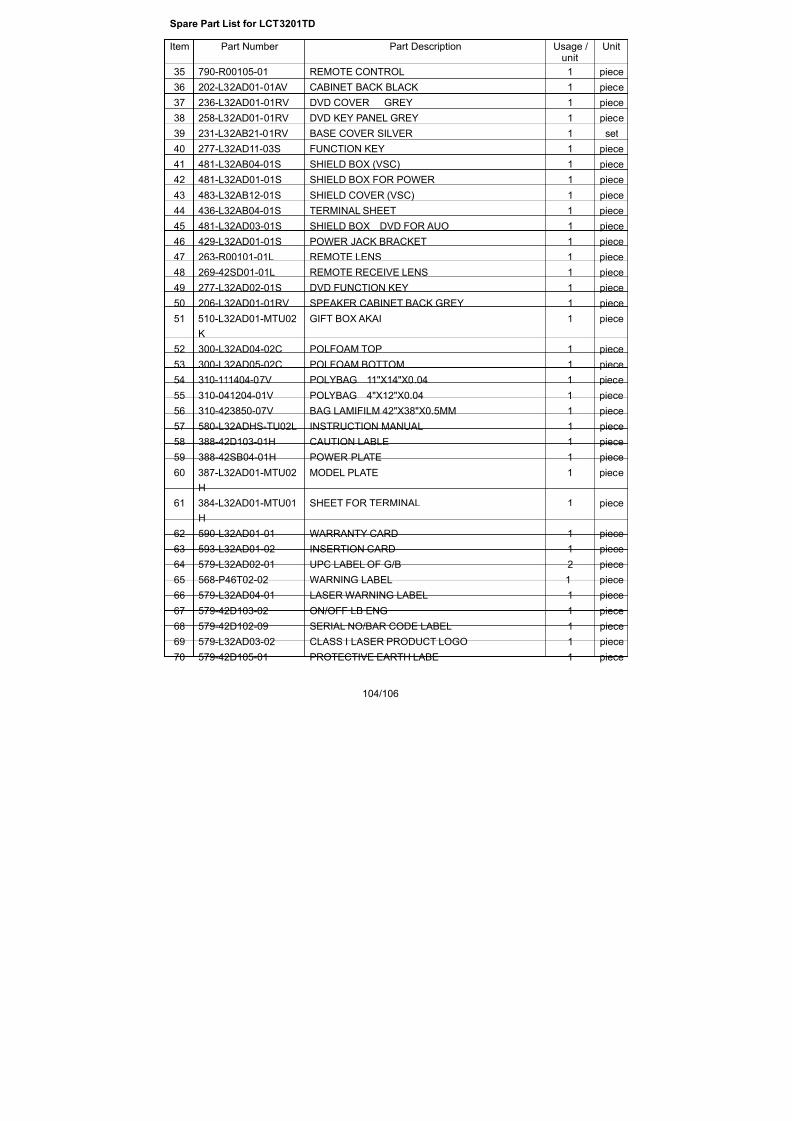
8/18/2019 Akai Lcd Tv Lct3201td_service Masnual
http://slidepdf.com/reader/full/akai-lcd-tv-lct3201tdservice-masnual 106/108
Spare Part List for LCT3201TD
Item Part Number Part Description Usage /unit
Un
35 790-R00105-01 REMOTE CONTROL 1 piec
36 202-L32AD01-01AV CABINET BACK BLACK 1 piec
37 236-L32AD01-01RV DVD COVER GREY 1 piec
38 258-L32AD01-01RV DVD KEY PANEL GREY 1 piec
39 231-L32AB21-01RV BASE COVER SILVER 1 se
40 277-L32AD11-03S FUNCTION KEY 1 piec
41 481-L32AB04-01S SHIELD BOX (VSC) 1 piec
42 481-L32AD01-01S SHIELD BOX FOR POWER 1 piec
43 483-L32AB12-01S SHIELD COVER (VSC) 1 piec
44 436-L32AB04-01S TERMINAL SHEET 1 piec
45 481-L32AD03-01S SHIELD BOX DVD FOR AUO 1 piec
46 429-L32AD01-01S POWER JACK BRACKET 1 piec
47 263-R00101-01L REMOTE LENS 1 piec
48 269-42SD01-01L REMOTE RECEIVE LENS 1 piec
49 277-L32AD02-01S DVD FUNCTION KEY 1 piec
50 206-L32AD01-01RV SPEAKER CABINET BACK GREY 1 piec
51 510-L32AD01-MTU02
K
GIFT BOX AKAI 1 piec
52 300-L32AD04-02C POLFOAM TOP 1 piec
53 300-L32AD05-02C POLFOAM BOTTOM 1 piec
54 310-111404-07V POLYBAG 11"X14"X0.04 1 piec
55 310-041204-01V POLYBAG 4"X12"X0.04 1 piec
56 310-423850-07V BAG LAMIFILM 42"X38"X0.5MM 1 piec
57 580-L32ADHS-TU02L INSTRUCTION MANUAL 1 piec
58 388-42D103-01H CAUTION LABLE 1 piec
59 388-42SB04-01H POWER PLATE 1 piec
60 387-L32AD01-MTU02
H
MODEL PLATE 1 piec
61 384-L32AD01-MTU01
H
SHEET FOR TERMINAL 1 piec
62 590-L32AD01-01 WARRANTY CARD 1 piec
63 593-L32AD01-02 INSERTION CARD 1 piec
64 579-L32AD02-01 UPC LABEL OF G/B 2 piec
65 568-P46T02-02 WARNING LABEL 1 piec
66 579-L32AD04-01 LASER WARNING LABEL 1 piec
67 579-42D103-02 ON/OFF LB ENG 1 piec
68 579-42D102-09 SERIAL NO/BAR CODE LABEL 1 piec
69 579-L32AD03-02 CLASS I LASER PRODUCT LOGO 1 piec
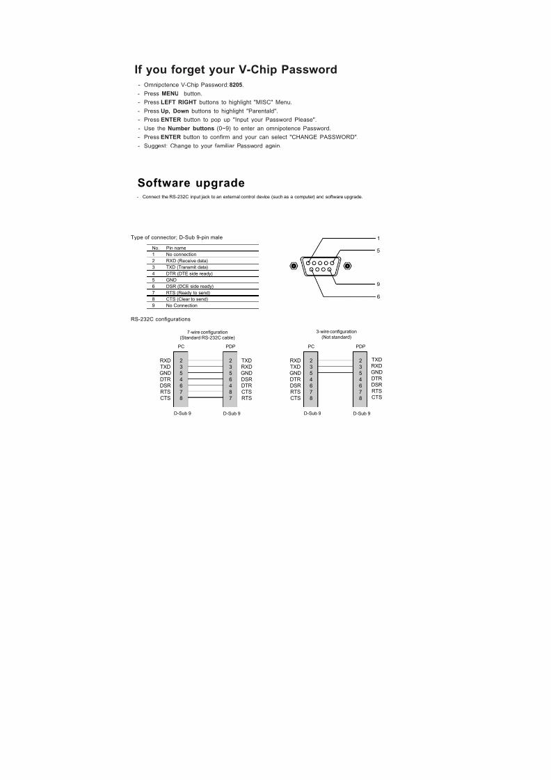
8/18/2019 Akai Lcd Tv Lct3201td_service Masnual
http://slidepdf.com/reader/full/akai-lcd-tv-lct3201tdservice-masnual 107/108

8/18/2019 Akai Lcd Tv Lct3201td_service Masnual
http://slidepdf.com/reader/full/akai-lcd-tv-lct3201tdservice-masnual 108/108
Software upgrade Process
- Power Switch OFF.
- Connect the serial port of the control device to the RS-232 jack on the LCD-TV back panel.
RS-232C connection cables are not supplied with the LCD-TV.
- Power Switch ON. The power indicator on the front of the panel should now display red, means
that the LCD-TV is in standby mode.
- Copy the software (MTKTOOL) to the computer.
- Open the software (MTKTOOL.EXE)
- Select MTK 8205 and Point "browse" on the interface of the MTKTOOL.exe.
- Select the file which will be update.
- Point "update" on the interface of the MTKTOOL.exe.
- Waiting for the upgrader programing, when it is finished, the bar will display 100%.
- After the upgrader is finished, shut down the power switch, take out the RS-232C connection
after the power indicator is extinguished.
Note: After upgrading, the first time of power on will be some long.


![Akai Cmo Lcd Tv Service Manual[1]](https://img.pdfslide.net/doc/110x75/547f410bb47959ac508b4e3c/akai-cmo-lcd-tv-service-manual1.jpg)