Embed Size (px)
Citation preview

Comptes Rendus
Physique
Nicolas Bonod and Yuri Kivshar
All-dielectric Mie-resonant metaphotonicsVolume 21, issue 4-5 (2020), p. 425-442.
<https://doi.org/10.5802/crphys.31>
Part of the Thematic Issue:Metamaterials 1
Guest editors: Boris Gralak (CNRS, Institut Fresnel, Marseille, France)and Sébastien Guenneau (UMI2004 Abraham de Moivre, CNRS-Imperial College,London, UK)
© Académie des sciences, Paris and the authors, 2020.Some rights reserved.
This article is licensed under theCreative Commons Attribution 4.0 International License.http://creativecommons.org/licenses/by/4.0/
Les Comptes Rendus. Physique sont membres duCentre Mersenne pour l’édition scientifique ouverte
www.centre-mersenne.org

Comptes RendusPhysique2020, 21, n 4-5, p. 425-442https://doi.org/10.5802/crphys.31
Metamaterials 1 / Métamatériaux 1
All-dielectric Mie-resonant metaphotonics
Méta-photonique diélectrique avec des résonateurs
de Mie
Nicolas Bonod∗, a and Yuri Kivsharb, c
a Aix Marseille Univ, CNRS, Centrale Marseille, Institut Fresnel, 13013 Marseille,France
b Nonlinear Physics Center, Research School of Physics, Australian NationalUniversity, Canberra ACT 2601, Australia
c ITMO University, St. Petersburg 197101, Russia
E-mails: [email protected] (N. Bonod), [email protected] (Y. Kivshar)
Abstract. All-dielectric subwavelength structures made of high-refractive-index materials combine a uniqueset of advantages in comparison with their plasmonic counterparts. In particular, they can interact resonantlywith light through the excitation of both electric and magnetic multipolar Mie-type resonances. This reviewdiscusses novel approaches to manipulate light with Mie-resonant dielectric subwavelength structures,spanning from individual nanoparticles to metasurfaces, and covering a broad range of effects, from near-field energy enhancement to far-field beam shaping.
Résumé. Les matériaux diélectriques à indice de réfraction élevé peuvent interagir de manière résonnanteavec la lumière grâce à l’excitation de modes de Mie électriques et magnétiques. Cette revue présente un étatde l’art du contrôle de la lumière par les résonances électriques et magnétiques de Mie dans les nanostruc-tures diélectriques. Elle décrit tout d’abord la reproduction des conditions de Kerker pour un contrôle de ladiffusion avant ou arrière de la lumière. Elle décrit ensuite l’intérêt des résonances de Mie pour (i) le contrôlede l’interaction entre la lumière et la matière dans les antennes optiques diélectriques (exaltation de champproche, densité d’états et directivité d’émission), (ii) la génération d’états photoniques liés dans le continuumou encore (iii) la génération de couleurs structurelles par des métasurfaces diélectriques.
Keywords. All-dielectric nanophotonics, Mie resonances, Kerker effect, Bound states in the continuum,Metaphotonics, Metasurfaces.
Mots-clés. Nanophotonique diélectrique, Résonances de Mie, Conditions de Kerker, Etats liés dans le contin-uum, Métaphotonique, Métasurfaces.
∗Corresponding author.
ISSN (electronic) : 1878-1535 https://comptes-rendus.academie-sciences.fr/physique/

426 Nicolas Bonod and Yuri Kivshar
1. Introduction
All-dielectric metamaterials were proposed in the 2000’s to achieve an artificial optical mag-netism without metals [1, 2]. They were based on materials with high values of dielectric per-mittivity, typically larger than 100. Composite materials with such high dielectric permittivitieswere proven to yield negative permeabilities when applying an effective medium theory [2]. Un-fortunately, common materials studied in the visible and near infrared (near-IR) spectra featuremuch smaller values of dielectric permittivity, typically smaller than 20. This constraint limitedthe soar of all-dielectric metamaterials in the visible and near-IR spectra.
However, it was highlighted also in the 2010’s that silicon (Si) nanoparticles feature low-orderelectric and magnetic Mie resonances [3–8] which can also be employed for the realization ofoptical magnetism, although Si exhibits much smaller dielectric permittivities (typically around12). Soon after, in 2012 the first experimental observations with dark-field spectroscopy of astrong magnetic response of individual Si particles were reported by two experimental groups [9,10]. The spectral response observed with dark-field spectroscopy in the visible and near-IRspectra evidenced several peaks associated with low-order electric and magnetic Mie resonances.In particular, the possibility to excite both electric or magnetic resonances, and to balancethe weight between the electric and magnetic dipolar modes to tailor the scattering propertiesof the particles triggered a huge interest. The resonant interaction of electromagnetic waveswith high-index nanostructures offers the possibility to engineer and control their phase andamplitude [11]. The possibility to combine electric and magnetic resonances inside the samedielectric nanostructure opened novel routes to develop planar metasurfaces able to tailor thephase of light as well as its transmittance and reflectance spectra.
Soon after, the field of “all-dielectric metamaterials”, based on effective averaged parame-ters, has been replaced naturally by “metaphotonics” (or “meta-optics”, also called “Mie-tronics”)where not averaged parameters but individual resonances become important. This field is in-spired by the physics of the magnetic dipole resonances and optical magnetism originating fromthe resonant dielectric nanostructures with high refractive index [12]. The concepts of meta-optics and all-dielectric resonant nanophotonics are driven by the idea to employ subwave-length dielectric Mie-resonant nanoparticles as “meta-atoms” for creating highly efficient op-tical metadevices, and the term “meta” is attributed to the importance of an optically-inducedmagnetic response.
Because of the unique optical resonances and their various combinations employed for re-alizing interference effects and strong localization of the electromagnetic fields, high-indexnanoscale structures are expected to complement or even replace different plasmonic compo-nents in a range of potential applications. Moreover, many concepts developed for plasmonicstructures, but fell short of their potential due to strong losses of metals at optical frequencies,can now be realized with Mie-resonant dielectric structures.
2. Mie resonances
Light scattering by small particles is a fundamental problem in optics and electromagnetism. Itcan be studied by solving Maxwell’s equations in the spherical coordinates. This theory, calledmultipolar theory or Mie theory, was developed originally by Gustav Mie in 1908 [13] andimproved by several contributors all over the XXth century [14, 15].
Spherical microstructures host high-order multipolar resonances associated with extremelyhigh quality factors (Q factors) that are called whispering gallery modes. They are observed inalmost lossless dielectrics such as silica or silicon nitride microstructured in microspheres ormicrodisks [16, 17]. When decreasing the size of the dielectric cavities from the micro to thesub-micrometer scale, the strength of the resonance weakens with refractive index typically
C. R. Physique, 2020, 21, n 4-5, 425-442

Nicolas Bonod and Yuri Kivshar 427
considered in whispering gallery modes (typically around n ≈ 1.3 and n ≈ 1.9). The order ofthe excited mode decreases with the size. The smallest size of an optical resonator is achievedwhen the lowest mode is excited. However, an efficient excitation of a low-order mode requiresan increase of the refractive index, typically from 1.5 to values larger than 2.2 and ideally largerthan 3. In the visible and near-IR spectra, semi-conductors such as silicon or germanium exhibitrefractive index ranging between 3 and 4 while some oxides also feature nice optical propertiessuch as titania.
Efficient resonant light-matter interactions at the nanoscale can be achieved for low-orderresonances in sub-micrometer sized particles. Compared with high order multipolar whisperinggallery modes, low-order resonances are characterized by smaller Q factors and a wider spectralresponse (see Figures 1(a–d)). The scattering cross section of a single dielectric particle is plottedin Figure 1(a), where R is the radius of a spherical particle. Several peaks can be observed overthe visible spectrum. A multipolar decomposition of the scattered field (see Figure 1(b)) allows toidentify the nature of the mode associated with each peak. When decreasing the wavelength, i.e.for the largest ratio between the wavelength and size of the scatterer, the first peak correspondsto the excitation of the magnetic dipolar mode, the second peak to the electric dipolar mode. TheMie resonances can also be obtained in non-spherical scatterers. This property results from thefact that the interest is brought in low-order resonances. Such resonances are less sensitive tohigh spatial frequencies than high-order multipolar resonances. That is the reason why a largeset of geometries has been investigated to tailor low-order Mie resonances.
Spherical silicon particles can be fabricated with the laser ablation technique [19]. This tech-nique is very convenient since it allows to disperse particles on glass cover-slips and to performdark-field optical spectroscopy, see Figure 1(c). It is enlightening to observe such well definedelectric and magnetic resonances that nicely match the numerical calculations. If the first inter-est of Mie resonances was brought in their far field response to retrieve for example the so-calledKerker conditions, one of the main interest of such resonances is to yield strong field intensitiesinside high-refractive-index materials.
It turns out that the terminology of “Mie resonance” is classically employed for describing res-onances in dielectric particles. However, we stress that plasmonic and dielectric resonances canboth be described by the Mie theory. In a sake of illustration, let us consider a silver particle at thefrequency that maximizes its dipolar plasmonic resonances, i.e. at the frequency that maximizesits dipolar electric Mie coefficient a1. It turns out that a dielectric scatterer can also maximize thisMie coefficient. An analytic expression between the two dielectric permittivities, of positive andnegative real parts, derived in Ref. [18], permits to calculate the dielectric permittivity that max-imizes the electric dipolar resonance, or in other words, the plasmonic resonance. The calcula-tion of the scattering cross-section of the metallic and dielectric particles displayed in Figure 1(d)shows that the two particles can exhibit the same optical response. However, the magnetic re-sponse is almost negligible with spherical metallic particles and strong magnetic responses canbe obtained only with more complex geometries.
The field of plasmonic metamaterials has investigated different geometries to overcome thislimitation and to yield a strong magnetic response. Among a wide variety of plasmonic shapes,one can cite the U - and the Ω-shaped scatterers [20, 21]. Coupling a set of plasmonic scatter-ers that exhibit a resonant electric polarizability is also an efficient way to yield artificial mag-netism [22]. The terminology employed to describe this effect is inspired by molecular chemistrywhere electronic orbitals of different atoms can couple. The coupling modifies the energy of theelectronic orbitals and leads to the formation of bonding and anti-bonding chemical bonds [23].The set of plasmonic scatterers is therefore called “plasmonic oligomers”. This field of researchaims at engineering the coupling between the different modes of the plasmonic scatterers to op-timize either the electric or magnetic response of the plasmonic oligomers.
C. R. Physique, 2020, 21, n 4-5, 425-442

428 Nicolas Bonod and Yuri Kivshar
Figure 1. Scattering properties of subwavelength particles. (a) Scattering efficiency spectraof a spherical Si particle with the radius R in air. (b) Extinction and scattering spectra ofa Si particle with R = 65 nm. The arrows indicate the electric dipole (ed) and magneticdipole (md) contributions to the total efficiencies. Adapted with permission from [3].(c) Experimental reflectance spectra of a 208 nm Si sphere on a glass substrate. Inset:Scanning Electron Microscopy (SEM) image of the corresponding Si nanoparticle anddark-field microscopic images. Adapted with permission from [10]. (d) Equivalence of Mieresonances in plasmonic and dielectric particles. Scattering cross-section with respect tothe wavelength. Dotted line: silver particle A with ε=−2.5+0.5i ; Solid blue line: dielectricparticle B with ε= 112+0.5i . Both particles have the same diameter: 50 nm. Adapted withpermission from [18].
The ability of spherical dielectric particles to yield a strong magnetic response is one of themain feature of Mie resonances. This property is at the core of many investigations with dielectricnanostructures to tailor the light scattering through the coherent excitation of electric and mag-netic modes and also to enhance the magnetic interaction between matter and electromagneticwaves, i.e. the wave-matter interaction via the magnetic component of the field. The magneticmode yields a strong magnetic response in the near field of the dielectric scatterer. The magneticfield distribution can be engineered and strong magnetic field intensities can be obtained. Thestrong magnetic response can also be used to engineer the magnetic local density of states andto promote magnetic spontaneous emission of quantum emitters. In the far field, the coherentexcitation of both electric and magnetic dipoles leads to unique scattering properties.
C. R. Physique, 2020, 21, n 4-5, 425-442

Nicolas Bonod and Yuri Kivshar 429
3. Kerker effect and Kerker conditions
In 1983, Milton Kerker and co-authors [24] discovered an interesting effect in the scattering ofelectromagnetic waves by a spherical particle made of a magnetic material characterized by mag-netic permeability µ and dielectric permittivity ε. This study revealed very unusual effect, nowa-days called Kerker effect. More specifically, Kerker and his collaborators revealed the possibilityto redirect the scattered radiation to either forward or backward direction, depending on the fre-quency. They discovered two conditions, known as the first and second Kerker conditions. Thefirst Kerker condition corresponds to a cancellation of the backward scattering (with a maximumin the forward scattering), while the second Kerker condition corresponds to a deep minimumin the forward scattering direction. The backward and forward scattering are defined by the scat-tering along the axis of the incoming waves. The optical theorem states that the extinction cross-section of a scatterer can be cast with respect to its forward scattering, which means that the for-ward scattering cannot be canceled. Kerker and co-workers established that the first condition isobtained when ε=µ, and the second condition is satisfied when
ε=−µ−4
µ+1.
Initially, this important study did not find a wide audience due to a lack of required magneticmaterials, and also because the Kerker conditions require special values of the parameters.
Nevertheless, as was shown independently by two groups in 2011, the Kerker conditionscan be extended to nonmagnetic dielectric spheres supporting both electric and magnetic Mieresonances [6, 25, 26]. This property of Mie scatterers to satisfy both Kerker conditions due to theelectric and magnetic Mie resonances was actually one of the first unusual property investigatedin this new field of all-dielectric metaphotonics. The artificial magnetism provided by the Mieresonances allows to mimic the anomalous scattering properties of magnetic spheres.
The Kerker conditions are predicted through the calculation of the electric and magneticpolarisabilities of the dielectric scatterer, αe and αh , respectively. It is convenient to derive theelectric and magnetic polarisabilities from the elements of the T (e,h)
n matrix (e and h standing forelectric and magnetic respectively), conventionally noticed an and bn , with n standing for themultipolar orders:
αe =−T (e)n = 3iεa1
2k3 , αh =−T (h)n
3ib1
2µk3 .
For a dipolar scatterer, i.e. a scatterer for which the multipolar Mie scattering coefficients an andbn can be safely neglected for n ≥ 2, the first Kerker condition is obtained when a1 = b1 whilethe second Kerker condition satisfies the relations: ℜ(ε−1αe ) =−ℜ(µαm) and ℑ(ε−1αe ) =ℑ(µαm)[25,26]. These analytical derivations can be assessed by calculating and the scattering patterns ofa single sphere at the first and second Kerker conditions [29] and first observed experimentally formicrowaves [25, 30]. Experimental values of the scattered intensity of a sphere can be matchedwell with the theoretical results, as shown in Figures 2(a,b). Experimental observations of theKerker conditions in the visible spectrum has been reported for Si and GaAs nanoparticles [27,31].In Ref. [27], an AlGaAs particle was fabricated by reactive ion etching followed by a transfer ona transparent fused silica substrate. Bright field spectroscopy on a single particle allowed themeasurement of the reflected spectrum and the observation of a cancellation of the reflectedintensity in a short spectral range [27].
The first Kerker condition finds straightforward applications in the design of Huygens sourcesin planar metasurfaces [32]. This condition meets several conditions that make dipolar Miescatterers ideal candidates to build metasurfaces: besides their weak losses, they can scatter lightin the forward direction, with a maximum of forward light scattering when a1 = b1 while thephase of the polarisability of a dipolar scatterer experiences a phase shift of π at a resonance.
C. R. Physique, 2020, 21, n 4-5, 425-442

430 Nicolas Bonod and Yuri Kivshar
Figure 2. Kerker effects in dielectric nanoantennas. (a) Evidence of the Kerker effect in agermanium sphere. Scattering diagram plotted for the two polarization cases (TE (blue)and TM (red)) when illuminating a 140 nm Ge sphere at the wavelengths λ = 2193 nm(top; forward scattering) and λ = 1823 nm (bottom; backward scattering). Adapted withpermission from [25]. (b) Observation of the Kerker effect in optics. Left: Spectrum of lightintensity backscattered by an individual GaAs nanodisk of radius 90 nm. Black dotted curve:measurement; red curve: numerical spectrum. Right: sketch of the measurement: whitelight is weakly focused on a GaAs particle. Backscattered light is separated by a 50/50 beam-splitter and sent to a spectrometer. Adapted with permission from [27]. (c) Concept of thetransverse Kerker effect. Electric dipole (ED) is in phase with a magnetic dipole (MD), andan electric quadrupole (EQ) is in phase with a magnetic quadrupole (MQ), whereas thedipoles are out of phase with the quadrupoles. Adapted with permission from [28].
When combining electric and magnetic resonances, the phase of the polarisability of a single Mieresonator can be tuned over 2π [32]. The forward light scattering being based on the excitationof both electric and magnetic dipolar resonances, this forward scattering can be associated witha strong modulation of the light phase. Efforts have been put to optimize the geometry of thescatterer to optimize the forward light scattering [33]. Regarding the second Kerker condition, wemention that besides the modulation of phase, it finds applications to develop highly refractivemetasurfaces [34].
The extension of the Kerker effect to other multipoles has been discussed in a number ofpapers, and these studies have been summarized recently [35]. Here, we also mention a re-cently demonstrated novel effect of the so-called transverse scattering of light by Mie-resonantsubwavelength particles with simultaneous suppression of both forward and backward scatter-ing [28]. This generalized Kerker effect occurs when in-phase electric and magnetic dipoles be-come out of phase with the corresponding pairs of quadrupoles. Shamkhi et al. [28] obtained thegeneral conditions for the simultaneous suppression of scattering in both forward and backwarddirections, and generalized these conditions to non-spherical particles, see Figure 2(c). They ver-ified the concept in a proof-of-principle microwave experiment, with good agreement with an-alytical and numerical results, and also studied metasurfaces composed of the nanoparticleswith the transverse scattering patterns. In a sharp contrast to Huygens’ metasurfaces, these novelmetasurfaces scatter neither forward nor backward, being almost invisible [36].
Subwavelength structures demonstrate many unusual optical properties which can be em-
C. R. Physique, 2020, 21, n 4-5, 425-442

Nicolas Bonod and Yuri Kivshar 431
ployed for a control of scattering of light and invisibility cloaking. Suppression of light scatter-ing can be achieved for a uniform dielectric object with high refractive index, based on the novelphysics of cascades of Fano resonances observed in the Mie scattering from a homogeneous di-electric rod [37]. Scattering cancellation and optical cloaking have been reported for a variety ofsystems based on dielectric metamaterials [38–40].
4. All-dielectric nanoantennas
Optical antennas are nanostructures aimed at manipulating spontaneous emission of solid-stateemitters at room temperature [41]. Plasmonic antennas were proposed early in the 2000’s, first toengineer the local density of states in the vicinity of metallic nanostructures [42–46], and secondto control the direction of emission of quantum emitters [47]. This field of research has led toimpressive results since metallic nanostructures can yield giant decay rates and can efficientlyshape the emission pattern. Among the wide range of metallic antennas, Yagi–Uda antennas andcorrugated antennas exhibit high gains in directivity [48, 49]. Self-assembled metallic particleswere also proved to yield extremely high decay rates, either with DNA template nanoantennasin which is grafted a single fluorescent molecule [50, 51], or with gap plasmons obtained bydepositing colloidal particles on metallic substrates and by inserting quantum emitters insidethe extremely small nanogap separating a metallic film from a colloidal particle [52, 53].
Electromagnetic Mie resonances experienced in dielectrics with weak losses are very promis-ing to develop highly radiative and directive optical antennas. The use of dielectric particles wasfirst investigated with silica microspheres that host high multipolar orders [54]. The use of higherrefractive index combined with a decrease of the size of dielectric particles was investigated nu-merically with a titania particle [55]. The titania particle was used to shape the emission patternof an electric dipole located in the nanogap of a silver dimer of nanoparticles. The dimer was usedto enhance the decay rates while the high refractive index was used to shape the emission direc-tion into a narrow lobe [55]. A hybrid metal-dielectric antenna was experimentally developed in2018 [56]. It was composed of a bow-tie gold nanoantenna coupled with 3 silicon nanorods. Thisantenna was fed by the photoluminescence of gold.
Silicon particles were numerically investigated in 2011 and 2012 to tailor the emission patternof electric dipolar emitters. By studying the emission pattern of an electric dipole coupled with asilicon particle hosting electric and magnetic dipolar modes, it was showed as early as 2011 thatthe direction of emission can be optimized either in the backward or the forward direction [6].The main interest of Mie resonant antennas comes from the possibility to couple the quantumemitter with both electric and magnetic modes [6–8]. The coherent excitation of electric andmagnetic modes offers a higher degree of freedom to engineer the emission in a given directionthrough the phase and amplitude of electric and magnetic modes. The coherent excitation ofelectric and magnetic dipoles can be seen as an extension of the Kerker conditions in the nearfield, i.e. when the Mie resonator is excited from the near field. The emission of a quantumemitter coupled with a dielectric Mie resonator can therefore be maximized in either the forwardor the backward directions. The gains in directivity that are obtained in these two conditions arehigher than those that could be achieved with an antenna hosting a single mode resonance, i.e.an electric dipole resonance like in the case of spherical plasmonic nanoparticles.
Besides their strong interest to shape the emission pattern of solid-state emitters, dielectricMie resonators are also very interesting to enhance the excitation strength of quantum emitters,to tailor their local density of states and to control their spontaneous emission rates. Whencompared with their plasmonic counterparts, the total decay rate enhancements yielded bydielectric antennas are smaller but the ratio between radiative and total decay rates can belarger thanks to smaller intrinsic losses. However, dielectric Mie resonators offer key properties
C. R. Physique, 2020, 21, n 4-5, 425-442

432 Nicolas Bonod and Yuri Kivshar
to manipulate spontaneous emission: (i) they can tailor decay rates of both electric and magneticdipolar transitions, (ii) they exhibit weak intrinsic losses and can efficiently collect the emittedphotons, (iii) semi-conductor based antennas can be easily integrated into photonic chips,(iv) internal fields can be engineered to boost the photoluminescence properties of emitterslocated inside the high refractive index material [57].
Controlling the electric or magnetic nature of the dipolar transition with Mie resonances, andmore generally controlling higher order transition moments, is an inspiring way of investiga-tion [58]. This field of research rapidly raised the interest since it coincided with the raise of in-terest in the higher order transition moments in rare earth ions [59–61]. Electric and magneticresonances of Mie resonators were therefore investigated to promote either an electric or a mag-netic transition of coupled rare-earth ions [62, 63]. However, from an experimental point of view,coupling rare earth ions with Mie resonators and more precisely locating the emitter at the posi-tion where the magnetic local density of states (LDOS) is maximum is very challenging. The mainachievements in the control of magnetic spontaneous emission were reported only recently witheither individual Si-based antennas [64] or Si-based metasurfaces [65].
If interest in Mie resonant antennas was initially driven by the original concept of magneticspontaneous emission, they also offer a strong interest to enhance the electric LDOS that issuitable to enhance fluorescence of quantum dots or molecules (see Figure 3). Taking inspirationfrom plasmonic nanogap antennas [50, 51, 69, 70], dielectric dimer antennas were proposed tomanipulate the spontaneous emission, as evidenced first numerically [62, 71] and in a secondstep experimentally [67, 68, 72]. The main challenge is to optimize the field outside the highrefractive index and to yield strong electric field intensities with a strong contrast with thebackground in order to detect fluorescence signal of molecules located in the nanogap (seeFigure 3). This method allows the enhancement of the electric field excitation on fluorescentmolecules and to increase by several orders of magnitude their fluorescence signal [68, 72].
If dielectric gap antennas are based on the strong enhancement of the electric field intensityin the gap separating the two particles, a major interest of Mie resonant antennas lies in the factthat they can be fed directly inside the cavity where the Purcell factor is maximum [73]. The firstresult was reported in 2017 with quantum dots embedded in silicon nanodisks [74]. Let us noticethat the concept of hybridization also applies to this case so that dimers and trimers of dopedSi-nanodisks can be coupled to further boost the photoluminescence of quantum dots. Thestrong enhancement of the internal field intensity driven by Mie resonances can also be exploitedto enhance the Raman signal of silicon particles [75, 76] and non linear signals. The richness ofthis field of research will undoubtedly lead to several outcomes in the upcoming years.
A very promising way of development is to consider active materials to design the photoniccavities (see Figure 4). For example, the high refractive index of diamond can be used to forma Mie resonant cavity around color centers [77, 78]. The resonant scattering of light on nanodi-amonds due to the excitation of electric and magnetic dipolar modes has been evidenced (seeFigure 4(a)). The photoluminescence of color centers can therefore benefit from Mie resonances.An enhancement of the photoluminescence of Nitrogen Vacancy (NV) color centers in nanodi-amonds was reported recently: the fluorescence efficiency can be enhanced thanks to Mie reso-nances and the emission lifetime can be decreased [79] (see Figure 4(b)).
A very promising approach for developing active Mie resonators is to consider halide per-ovskites, a class of semi-conductor materials characterized by a high refractive index. The dis-covery of the exceptional excitonic properties almost 10 years ago triggered a huge interest to im-prove the efficiency of photovoltaics and light emitting devices [80]. Halide perovskites feature ex-ceptional excitonic properties. Bridging the gap between this novel class of light emitting materi-als and Mie resonant cavities will lead to outcomes in integrated light sources [81]. Enhancementof the photoluminescence of halide perovskites was first reported in 2018 by considering par-
C. R. Physique, 2020, 21, n 4-5, 425-442

Nicolas Bonod and Yuri Kivshar 433
Figure 3. All-dielectric nanogap antennas. (a) Electric field distribution in the vicinity ofa 20 nm nanogap separating two Si microdisks (diameter 2 µm, thickness of 200 nm)illuminated in normal incidence with an incident electric field linearly polarized along thex-axis at a wavelength of 2.437 µm. Adapted with permission from [66]. (b) SEM imageof a silicon nanogap antenna fabricated with e-beam lithography. Diameter of 170 nmdiameter, thickness of 60 nm and nanogap of 20 nm. (c) Enhancement of the electricfield intensity yielded by a GaP dimer antenna composed of two GaP pillars, 100 nm indiameters, 200 nm in height and separated by a 35 nm nanogap. The field distributionis taken at mid-height (100 nm). Adapted with permission from [67]. (d) Brightness peremitter with respect to the emission power for two different nanogap lenghts, 20 nm and30 nm, with the Si dimer nanogap antenna displayed in (b). Comparison with the brightnessper emitter measured without antenna (measured signal × 50). Adapted with permissionfrom [68].
ticles made of MAPbI3 created by using a laser ablation technique on a perovskite thin film. Amaximum of the photoluminescence signal was reported at the wavelength corresponding to thequadrupolar magnetic resonance [82]. The next challenge after performing Mie enhanced photo-luminescence lies in the stimulated emission and the development of a novel class of laser cavi-ties by forming Mie cavities in halide perovskites. The latest results were obtained with nanocubesmade of CsPbBr3 (see Figures 4(c–e)). High quality monocrystalline CsPbBr3 nanocubes are firstsynthesized chemically on a sapphire substrate (see Figure 4(c)). Dark field spectrum performedon a single 420 nm nanocube displayed in Figure 4(d) clearly evidences the resonant light scat-tering due to the excitation of electric and magnetic multipoles. The photoluminescence spec-trum of CsPbBr3 is indicated by the green zone in Figure 4(d). A peak of the dark field spectrumcan be observed in this spectral range. The resonant light scattering is assessed by observing astrong dependence of the scattering spectra on the size of the nanocubes. The photolumines-cence spectra are recorded when exciting nanocubes with a 150 fs laser. Importantly, the spectra
C. R. Physique, 2020, 21, n 4-5, 425-442

434 Nicolas Bonod and Yuri Kivshar
Figure 4. Mie resonances in excitonic materials: colored centers in nanodiamonds (toprow) and perovskites (bottom row). (a) Unpolarized scattering spectrum of a single nanodi-amond. Black line: experimental spectrum. Red line: numerical simulations implementedwith FDTD (Finite Difference Time Domain) when considering a spherical nanodiamondwith a diameter of 320 nm under the experimental conditions of the collection. Adaptedwith permission from [77]. (b) Time-resolved photoluminescence measurements for twosets of samples: NV centers in optically small (<100 nm) nanodiamonds (orange dots)and in large and optically resonant nanodiamonds (purple dots). Adapted with permissionfrom [79]. (c) SEM images of CsPbBr3 nanocubes placed on a sapphire substrate. Scale baris 500 nm. (d) Dark-field spectra of the CsPbBr3 nanocubes. The photoluminescence spec-tral range is indicated by the green zone. Pump intensity-dependent emission spectra forthree different fluences compared with the lasing threshold: above (red), equal (orange)and below (green) the lasing threshold. (c–e) Adapted with permission from [83].
reveal a threshold-like appearance of a photoluminescence signal in the range λ= (532;538) nm,that corresponds to the red side of the emission line of the exciton (see Figure 4(e)).
5. Bound states in the continuum
Bound states in the continuum have attracted a lot of attention in photonics recently, and theyoriginate from a coupling between the leaky modes in dielectric structures such as photoniccrystals, metasurfaces, and isolated resonators [84]. These resonances provide an alternativemean to achieve very large Q factors for lasing [85] and also allow to tune a photonic system intothe regime of the so-called supercavity mode [86]. A true bound state in the continuum (BIC) is amathematical object with an infinite value of the Q factor and vanishing resonance width, and itcan exist only in ideal loss-less infinite structures or for extreme values of parameters [87, 88]. Inpractice, BIC can be realized as a quasi-BIC mode, being directly associated with the supercavity
C. R. Physique, 2020, 21, n 4-5, 425-442

Nicolas Bonod and Yuri Kivshar 435
mode [86], when both the Q factor and resonance width become finite. However, the localizationof light inspired by the BIC physics makes it possible to realize high-Q quasi-BIC modes in manyoptical structures such as cavities and coupled waveguides.
Importantly, there exists a direct link between quasi-BIC states and Fano resonances sincethese two phenomena are supported by the similar physics. More specifically, quasi-BIC reso-nance can be described explicitly by the classical Fano formula, and the observed peak positionsand linewidths correspond exactly to the real and imaginary parts of the eigenmode frequencies.The Fano parameter becomes ill-defined at the BIC condition, which corresponds to a collapse ofthe Fano resonance. Importantly, every quasi-BIC modes can be linked with the Fano resonances,whereas the opposite is not always true: the Fano resonance may not converge to the BIC modefor any variation of the system parameters.
As an example, we consider all-dielectric metasurfaces with the in-plane symmetry break-ing [89] that can support sharp high-Q resonances arising from a distortion of symmetry-protected BICs. We follow the recent paper [90], we consider a metasurface made of As2S3 andplaced on a glass substrate consisting of a square lattice of meta-atoms with broken in-plane in-version symmetry, as illustrated in Figure 5(a). The meta-atom is constructed of a pair of rect-angular bars which have lengths L and L − δL, respectively. The asymmetry of the unit cell iscontrolled by the difference in bar lengths, which is characterized by the asymmetry parameterα= δL/L, see Figure 5(b).
Figure 5(c) demonstrates the dependence of the simulated transmission spectra on the wave-length of excitation and the asymmetry parameter α. The white dashed line illustrates the eigen-mode dispersion. The eigenmode simulations show that the metasurface with a symmetric unitcell (α= 0) supports a symmetry-protected BIC at 795 nm, which has infinite Q factor and is notmanifested in the transmission spectrum. The BIC is unstable against perturbations that breakthe in-plane inversion symmetry, so for α > 0 it transforms into a quasi-BIC with a finite Q fac-tor [89]. The quasi-BIC is revealed in the transmission spectra as a sharp resonance with a Fanolineshape whose linewidth increases with the magnitude of asymmetry. The dependence of theradiative Q factor on α follows the inverse quadratic law for small values of the asymmetry pa-rameter [89], as shown in Figure 5(d). Hence, the meta-atom asymmetry is necessary to obtain asharp resonance whose position and width can be adjusted by the degree of asymmetry.
Thus, bound states in the continuum provide a new approach for engineering a resonantresponse of dielectric metasurfaces composed of meta-atoms with broken in-plane inversionsymmetry. The similar approach can be applied to the case of nonlinear metasurfaces [91, 92]with broken-symmetry or nonlinear metasurfaces composed of arrays of chalcogenide nanores-onators designed for the nonlinear optical generation of higher harmonics.
6. Applications of Mie resonances: structural colors
Colors perceived by eyes result from the interaction between the incoming light and the threetypes of cone cells. A modification in the spectrum of the incoming light will result in a modifica-tion of the perceived color. When white light interacts with structured matter, its broad spectrumexperiences a strong variation with peaks and dips which yield a color to the nanostructured mat-ter. Colors resulting from the interaction between light and nano or microstructures are calledstructural colors. The terminology “structural” means that the color depends on the morphologyof the structured matter. A modification of the morphology modifies the structural color. Struc-tural colors can be found in a wide set of biological species, the most famous example being cer-tainly the wings of the Morpho butterfly [93, 94]. Wings are structured at a sub-micrometer scalewhich provides photonic band gaps. In the case of the Morpho butterfly, the photonic band gap
C. R. Physique, 2020, 21, n 4-5, 425-442

436 Nicolas Bonod and Yuri Kivshar
Figure 5. Metasurfaces with bound states in the continuum. (a) Design of a metasurfaceconsisting of a square array of As2S3-bar pairs of different length placed on a glass sub-strate. The inset shows the orientation and polarization of the incident field. (b) Defini-tion of the asymmetry parameter α. (c) Numerically simulated transmission spectra withrespect to the excitation wavelength and the asymmetry parameter α. The white dashedline illustrates the quasi-BIC dispersion. (d) Dependence of the radiative Q factor on theparameter α. The dashed line shows an inverse quadratic fitting. Adapted with permissionfrom [90].
is centered on the blue part of the spectrum. The blue part of the spectrum is therefore reflectedwhich provides a vivid blue color to the wings.
Structural colors can also be found in plasmonics. When observing metallic particles ofdifferent sizes and shapes dispersed in a transparent substrate in dark field spectroscopy, amyriad of colors can be observed. It turns out that each particle yields its own color and behaveslike a colored pixel. The pixel size stands under the diffraction limit and achieves the limit ofresolution. This approach is very promising to create non fading colors with a high resolution.When assembling different scatterers on a surface, colored images can be finely designed whichopens plenty of rooms to create images at high resolution [95]. Structural colors have benefitedfrom intense developments to extend the gamut of colors, to decrease the cost of this technologyand to extend its range of applications [96].
When observing silicon particles in dark-field spectroscopy, structural colors can also beobserved (see Figure 1) [9, 10, 19, 97]. This result was expected since their resonant interactionwith light strongly modulates the scattered spectrum. The coupling of light with electric andmagnetic Mie resonant modes of high-index particles results in a perceived color that can becontrolled through the shape and composition of the particles, and also through their mutualcoupling. This result strengthens the field of resonant structural colors since cost effective and
C. R. Physique, 2020, 21, n 4-5, 425-442
Nicolas Bonod and Yuri Kivshar 437
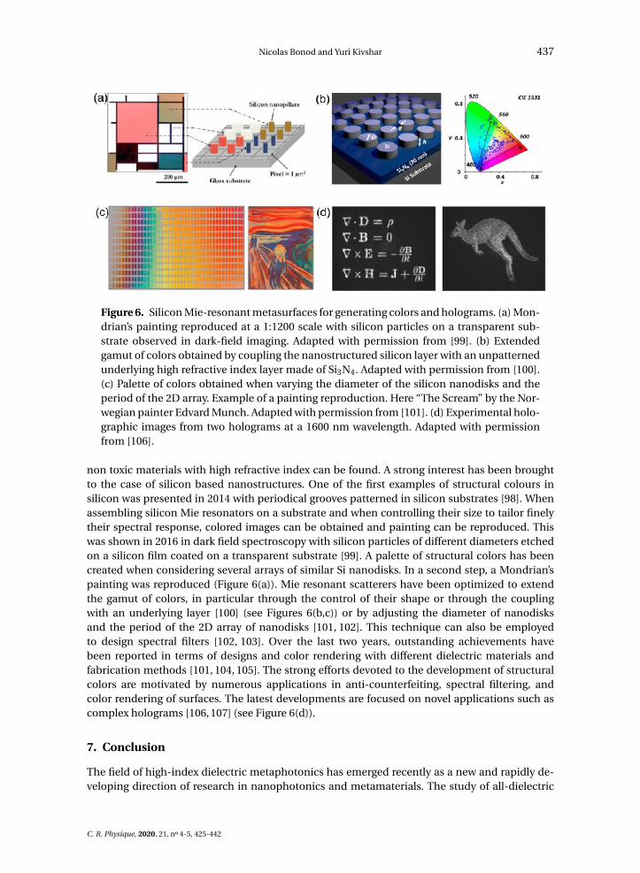
Figure 6. Silicon Mie-resonant metasurfaces for generating colors and holograms. (a) Mon-drian’s painting reproduced at a 1:1200 scale with silicon particles on a transparent sub-strate observed in dark-field imaging. Adapted with permission from [99]. (b) Extendedgamut of colors obtained by coupling the nanostructured silicon layer with an unpatternedunderlying high refractive index layer made of Si3N4. Adapted with permission from [100].(c) Palette of colors obtained when varying the diameter of the silicon nanodisks and theperiod of the 2D array. Example of a painting reproduction. Here “The Scream” by the Nor-wegian painter Edvard Munch. Adapted with permission from [101]. (d) Experimental holo-graphic images from two holograms at a 1600 nm wavelength. Adapted with permissionfrom [106].
non toxic materials with high refractive index can be found. A strong interest has been broughtto the case of silicon based nanostructures. One of the first examples of structural colours insilicon was presented in 2014 with periodical grooves patterned in silicon substrates [98]. Whenassembling silicon Mie resonators on a substrate and when controlling their size to tailor finelytheir spectral response, colored images can be obtained and painting can be reproduced. Thiswas shown in 2016 in dark field spectroscopy with silicon particles of different diameters etchedon a silicon film coated on a transparent substrate [99]. A palette of structural colors has beencreated when considering several arrays of similar Si nanodisks. In a second step, a Mondrian’spainting was reproduced (Figure 6(a)). Mie resonant scatterers have been optimized to extendthe gamut of colors, in particular through the control of their shape or through the couplingwith an underlying layer [100] (see Figures 6(b,c)) or by adjusting the diameter of nanodisksand the period of the 2D array of nanodisks [101, 102]. This technique can also be employedto design spectral filters [102, 103]. Over the last two years, outstanding achievements havebeen reported in terms of designs and color rendering with different dielectric materials andfabrication methods [101, 104, 105]. The strong efforts devoted to the development of structuralcolors are motivated by numerous applications in anti-counterfeiting, spectral filtering, andcolor rendering of surfaces. The latest developments are focused on novel applications such ascomplex holograms [106, 107] (see Figure 6(d)).
7. Conclusion
The field of high-index dielectric metaphotonics has emerged recently as a new and rapidly de-veloping direction of research in nanophotonics and metamaterials. The study of all-dielectric
C. R. Physique, 2020, 21, n 4-5, 425-442

438 Nicolas Bonod and Yuri Kivshar
resonant nanostructures is motivated by the rich physics of Mie resonances allowing to exciteboth electric and magnetic multipole modes in individual subwavelength particles. Metaphoton-ics has a broad range of applications, highlighting the importance of optically-induced magneticresponse, and including structural coloring, optical sensing, spatial modulation of light, nonlin-ear and active media, as well as both integrated classical and quantum circuitry and topologi-cal photonics, underpinning a new generation of highly-efficient active metadevices. We antici-pate further rapid development of these ideas into the field of active metaphotonics for creatingnew types of light sources, light-emitting metasurfaces, quantum signal processing, and efficientnanolasers.
References
[1] S. O’Brien, J. B. Pendry, “Photonic band-gap effects and magnetic activity in dielectric composites”, J. Phys.:Condens. Matter 14 (2002), no. 15, p. 4035.
[2] J. A. Schuller, R. Zia, T. Taubner, M. L. Brongersma, “Dielectric metamaterials based on electric and magneticresonances of silicon carbide particles”, Phys. Rev. Lett. 99 (2007), article ID 107401.
[3] A. B. Evlyukhin, C. Reinhardt, A. Seidel, B. S. Luk’yanchuk, B. N. Chichkov, “Optical response features of si-nanoparticle arrays”, Phys. Rev. B 82 (2010), article ID 045404.
[4] A. B. Evlyukhin, C. Reinhardt, B. N. Chichkov, “Multipole light scattering by nonspherical nanoparticles in thediscrete dipole approximation”, Phys. Rev. B 84 (2011), article ID 235429.
[5] A. García-Etxarri, R. Gómez-Medina, L. S. Froufe-Pérez, C. López, L. Chantada, F. Scheffold, J. Aizpurua, M. Nieto-Vesperinas, J. J. Sáenz, “Strong magnetic response of submicron silicon particles in the infrared”, Opt. Express 19(2011), no. 6, p. 4815-4826.
[6] A. Krasnok, A. Miroshnichenko, P. Belov, Y. Kivshar, “Huygens optical elements and Yagi–Uda nanoantennas basedon dielectric nanoparticles”, JETP Lett. 94 (2011), p. 593-598.
[7] B. Rolly, B. Stout, N. Bonod, “Boosting the directivity of optical antennas with magnetic and electric dipolar resonantparticles”, Opt. Express 20 (2012), no. 18, p. 20376-20386.
[8] A. E. Krasnok, A. E. Miroshnichenko, P. A. Belov, Y. S. Kivshar, “All-dielectric optical nanoantennas”, Opt. Express 20(2012), no. 18, p. 20599-20604.
[9] A. I. Kuznetsov, A. E. Miroshnichenko, Y. H. Fu, J. Zhang, B. Lukyanchuk, “Magnetic light”, Sci. Rep. 2 (2012), p. 492.[10] A. B. Evlyukhin, S. M. Novikov, U. Zywietz, R. L. Eriksen, C. Reinhardt, S. I. Bozhevolnyi, B. N. Chichkov, “Demon-
stration of magnetic dipole resonances of dielectric nanospheres in the visible region”, Nano Lett. 12 (2012), no. 7,p. 3749-3755.
[11] A. I. Kuznetsov, A. E. Miroshnichenko, M. L. Brongersma, Y. S. Kivshar, B. Luk’yanchuk, “Optically resonant dielectricnanostructures”, Science 354 (2016), no. 6314, article ID aag2472.
[12] S. Kruk, Y. Kivshar, “Functional meta-optics and nanophotonics governed by Mie resonances”, ACS Photon. 4(2017), p. 2638.
[13] G. Mie, “Beiträge zur optik trüber medien, speziell kolloidaler metallösungen”, Ann. Phys. 330 (1908), no. 3, p. 377-445.
[14] H. Hulst, Light scattering by small particles, Structure of matter series, Wiley, 1957.[15] A. Lagendijk, B. A. van Tiggelen, “Resonant multiple scattering of light”, Phys. Rep. 270 (1996), no. 3, p. 143-215.[16] A. B. Matsko, V. S. Ilchenko, “Optical resonators with whispering gallery modes i: basics”, IEEE J. Sel. Top. Quantum
Electron. 12 (2006), no. 3, p. 3.[17] V. S. Ilchenko, A. B. Matsko, “Optical resonators with whispering-gallery modes-part ii: applications”, IEEE J. Sel.
Top. Quantum Electron. 12 (2006), no. 1, p. 15-32.[18] A. Devilez, X. Zambrana-Puyalto, B. Stout, N. Bonod, “Mimicking localized surface plasmons with dielectric
particles”, Phys. Rev. B 92 (2015), no. 24, article ID 241412.[19] U. Zywietz, A. B. Evlyukhin, C. Reinhardt, B. N. Chichkov, “Laser printing of silicon nanoparticles with resonant
optical electric and magnetic responses”, Nat. Commun. 5 (2014), p. 3402.[20] F. B. Arango, A. F. Koenderink, “Polarizability tensor retrieval for magnetic and plasmonic antenna design”, New J.
Phys. 15 (2013), no. 7, article ID 073023.[21] J. Proust, N. Bonod, J. Grand, B. Gallas, “Optical monitoring of the magnetoelectric coupling in individual plasmonic
scatterers”, ACS Photon. 3 (2016), no. 9, p. 1581-1588.[22] M. Dubois, L. Leroi, Z. Raolison, R. Abdeddaim, T. Antonakakis, J. de Rosny, A. Vignaud, P. Sabouroux, E. Georget,
B. Larrat et al., “Kerker effect in ultrahigh-field magnetic resonance imaging”, Phys. Rev. X 8 (2018), no. 3, article ID031083.
C. R. Physique, 2020, 21, n 4-5, 425-442

Nicolas Bonod and Yuri Kivshar 439
[23] P. Nordlander, C. Oubre, E. Prodan, K. Li, M. Stockman, “Plasmon hybridizaton in nanoparticle dimers”, Nano Lett.4 (2004), no. 5, p. 899-903.
[24] M. Kerker, D.-S. Wang, C. L. Giles, “Electromagnetic scattering by magnetic spheres”, J. Opt. Soc. Am. 73 (1983),no. 6, p. 765-767.
[25] R. Gomez-Medina, B. Garcia-Camara, I. Suarez-Lacalle, F. Gonzalez, F. Moreno, M. Nieto-Vesperinas, J. J. Saenz,“Electric and magnetic dipolar response of germanium nanospheres: interference effects, scattering anisotropy,and optical forces”, J. Nanophoton. 5 (2011), article ID 053512.
[26] M. Nieto-Vesperinas, R. Gomez-Medina, J. J. Saenz, “Angle-suppressed scattering and optical forces on submicrom-eter dielectric particles”, J. Opt. Soc. Am. A 28 (2011), no. 1, p. 54-60.
[27] S. Person, M. Jain, Z. Lapin, J. J. Saenz, G. Wicks, L. Novotny, “Demonstration of zero optical backscattering fromsingle nanoparticles”, Nano Lett. 13 (2013), no. 4, p. 1806-1809.
[28] H. Shamkhi, K. Baryshnikova, A. Sayanskiy, P. Kapitanova, P. Terekhov, P. Belov, A. Karabchevsky, A. Evlyukhin,Y. Kivshar, A. Shalin, “Transverse scattering and generalized Kerker effects in all-dielectric mie-resonant metaop-tics”, Phys. Rev. Lett. 122 (2019), article ID 193905.
[29] R. Paniagua-Domínguez, F. López-Tejeira, R. Marqués, J. A. Sánchez-Gil, “Metallo-dielectric core-shell nanospheresas building blocks for optical three-dimensional isotropic negative-index metamaterials”, New J. Phys. 13 (2011),no. 12, article ID 123017.
[30] J. Geffrin, B. García-Cámara, R. Gómez-Medina, P. Albella, L. Froufe-Pérez, C. Eyraud, A. Litman, R. Vaillon,F. González, M. Nieto-Vesperinas et al., “Magnetic and electric coherence in forward-and back-scattered electro-magnetic waves by a single dielectric subwavelength sphere”, Nat. Commun. 3 (2012), p. 1171.
[31] Y. H. Fu, A. I. Kuznetsov, A. E. Miroshnichenko, Y. F. Yu, B. Lukyanchuk, “Directional visible light scattering by siliconnanoparticles”, Nat. Commun. 4 (2013), p. 1527.
[32] I. Staude, A. E. Miroshnichenko, M. Decker, N. T. Fofang, S. Liu, E. Gonzales, J. Dominguez, T. S. Luk, D. N. Neshev,I. Brener et al., “Tailoring directional scattering through magnetic and electric resonances in subwavelength siliconnanodisks”, ACS Nano 7 (2013), no. 9, p. 7824-7832.
[33] B. S. Luk’yanchuk, N. V. Voshchinnikov, R. Paniagua-Domínguez, A. I. Kuznetsov, “Optimum forward light scatteringby spherical and spheroidal dielectric nanoparticles with high refractive index”, ACS Photon. 2 (2015), no. 7, p. 993-999.
[34] P. Moitra, B. A. Slovick, W. Li, I. I. Kravchencko, D. P. Briggs, S. Krishnamurthy, J. Valentine, “Large-scale all-dielectricmetamaterial perfect reflectors”, ACS Photon. 2 (2015), no. 6, p. 692-698.
[35] W. Liu, Y. Kivshar, “Generalized kerker effects in nanophotonics and meta-optics”, Opt. Express 26 (2018), p. 13085-13105.
[36] H. K. Shamkhi, A. Sayanskiy, A. C. Valero, A. S. Kupriianov, P. Kapitanova, Y. S. Kivshar, A. S. Shalin, V. R. Tuz,“Transparency and perfect absorption of all-dielectric resonant metasurfaces governed by the transverse kerkereffect”, Phys. Rev. Mater. 3 (2019), no. 8, article ID 085201.
[37] M. Rybin, D. Filonov, P. Belov, Y. Kivshar, M. Limonov, “Switching from visibility to invisibility via fano resonances:Theory and experiment”, Sci. Rep. 5 (2015), p. 8774.
[38] Q. Zhao, J. Zhou, F. Zhang, D. Lippens, “Mie resonance-based dielectric metamaterials”, Mater. Today 12 (2009),p. 60-69.
[39] J. Valentine, J. Li, T. Zentgraf, G. Bartal, X. Zhang, “An optical cloak made of dielectrics”, Nat. Mater. 8 (2009), p. 568-571.
[40] M. M. Farhat, S. Muhlig, C. Rockstuhl, F. Lederer, “Scattering cancellation of the magnetic dipole field frommacroscopic spheres”, Opt. Express 20 (2012), p. 13896-13906.
[41] L. Novotny, N. van Hulst, “Antennas for light”, Nat. Photon. 5 (2011), no. 2, p. 83-90.[42] E. Dulkeith, A. Morteani, T. Niedereichholz, T. Klar, J. Feldmann, S. Levi, F. Van Veggel, D. Reinhoudt, M. Möller,
D. Gittins, “Fluorescence quenching of dye molecules near gold nanoparticles: radiative and nonradiative effects”,Phys. Rev. Lett. 89 (2002), no. 20, article ID 203002.
[43] P. Mühlschlegel, H. Eisler, O. Martin, B. Hecht, D. Pohl, “Resonant optical antennas”, Science 308 (2005), no. 5728,p. 1607-1609.
[44] P. Anger, P. Bharadwaj, L. Novotny, “Enhancement and quenching of single-molecule fluorescence”, Phys. Rev. Lett.96 (2006), article ID 113002.
[45] P. Bharadwaj, L. Novotny, “Spectral dependence of single molecule fluorescence enhancement”, Opt. Express 15(2007), no. 21, p. 14266-14274.
[46] M. Ringler, A. Schwemer, M. Wunderlich, A. Nichtl, K. Kürzinger, T. Klar, J. Feldmann, “Shaping emission spectra offluorescent molecules with single plasmonic nanoresonators”, Phys. Rev. Lett. 100 (2008), no. 20, article ID 203002.
[47] J. Li, A. Salandrino, N. Engheta, “Shaping light beams in the nanometer scale: A Yagi–Uda nanoantenna in theoptical domain”, Phys. Rev. B 76 (2007), article ID 245403.
[48] A. G. Curto, G. Volpe, T. H. Taminiau, M. P. Kreuzer, R. Quidant, N. F. van Hulst, “Unidirectional emission of aquantum dot coupled to a nanoantenna”, Science 329 (2010), no. 5994, p. 930-933.
C. R. Physique, 2020, 21, n 4-5, 425-442
440 Nicolas Bonod and Yuri Kivshar
[49] H. Aouani, O. Mahboub, N. Bonod, E. Devaux, E. Popov, H. Rigneault, T. W. Ebbesen, J. Wenger, “Bright unidirec-tional fluorescence emission of molecules in a nanoaperture with plasmonic corrugations”, Nano Lett. 11 (2011),no. 2, p. 637-644.
[50] M. P. Busson, B. Rolly, B. Stout, N. Bonod, S. Bidault, “Accelerated single photon emission from dye molecule-drivennanoantennas assembled on DNA”, Nat. Commun. 3 (2012), p. 962.
[51] G. Acuna, F. Möller, P. Holzmeister, S. Beater, B. Lalkens, P. Tinnefeld, “Fluorescence enhancement at docking sitesof DNA-directed self-assembled nanoantennas”, Science 338 (2012), no. 6106, p. 506-510.
[52] T. B. Hoang, G. M. Akselrod, M. H. Mikkelsen, “Ultrafast room-temperature single photon emission from quantumdots coupled to plasmonic nanocavities”, Nano Lett. 16 (2015), no. 1, p. 270-275.
[53] J. J. Baumberg, J. Aizpurua, M. H. Mikkelsen, D. R. Smith, “Extreme nanophotonics from ultrathin metallic gaps”,Nat. Mater. 18 (2019), p. 668-678.
[54] D. Gérard, A. Devilez, H. Aouani, B. Stout, N. Bonod, J. Wenger, E. Popov, H. Rigneault, “Efficient excitation andcollection of single-molecule fluorescence close to a dielectric microsphere”, J. Opt. Soc. Am. B 26 (2009), no. 7,p. 1473-1478.
[55] A. Devilez, B. Stout, N. Bonod, “Compact metallo-dielectric optical antenna for ultra directional and enhancedradiative emission”, ACS Nano 4 (2010), no. 6, p. 3390-3396.
[56] J. Ho, Y. H. Fu, Z. Dong, R. Paniagua-Dominguez, E. H. Koay, Y. F. Yu, V. Valuckas, A. I. Kuznetsov, J. K. Yang, “Highlydirective hybrid metal–dielectric Yagi–Uda nanoantennas”, ACS Nano 12 (2018), no. 8, p. 8616-8624.
[57] S. Bidault, M. Mivelle, N. Bonod, “Dielectric nanoantennas to manipulate solid-state light emission”, J. Appl. Phys.126 (2019), no. 9, article ID 094104.
[58] D. G. Baranov, R. S. Savelev, S. V. Li, A. E. Krasnok, A. Alù, “Modifying magnetic dipole spontaneous emission withnanophotonic structures”, Laser Photon. Rev. 11 (2017), no. 3, article ID 1600268.
[59] S. Karaveli, R. Zia, “Strong enhancement of magnetic dipole emission in a multilevel electronic system”, Opt. Lett.35 (2010), no. 20, p. 3318-3320.
[60] S. Karaveli, R. Zia, “Spectral tuning by selective enhancement of electric and magnetic dipole emission”, Phys. Rev.Lett. 106 (2011), article ID 193004.
[61] C. M. Dodson, R. Zia, “Magnetic dipole and electric quadrupole transitions in the trivalent lanthanide series:Calculated emission rates and oscillator strengths”, Phys. Rev. B 86 (2012), article ID 125102.
[62] B. Rolly, B. Bebey, S. Bidault, B. Stout, N. Bonod, “Promoting magnetic dipolar transition in trivalent lanthanide ionswith lossless mie resonances”, Phys. Rev. B 85 (2012), article ID 245432.
[63] M. K. Schmidt, R. Esteban, J. J. Sáenz, I. Suárez-Lacalle, S. Mackowski, J. Aizpurua, “Dielectric antennas - a suitableplatform for controlling magnetic dipolar emission”, Opt. Express 20 (2012), no. 13, p. 13636-13650.
[64] M. Sanz-Paz, C. Ernandes, J. U. Esparza, G. W. Burr, N. F. van Hulst, A. Maitre, L. Aigouy, T. Gacoin, N. Bonod, M. F.Garcia-Parajo et al., “Enhancing magnetic light emission with all-dielectric optical nanoantennas”, Nano Lett. 18(2018), no. 6, p. 3481-3487.
[65] A. Vaskin, S. Mashhadi, M. Steinert, K. E. Chong, D. Keene, S. Nanz, A. Abass, E. Rusak, D.-Y. Choi, I. Fernandez-Corbaton, T. Pertsch, C. Rockstuhl, M. A. Noginov, Y. S. Kivshar, D. N. Neshev, N. Noginova, I. Staude, “Manipulationof magnetic dipole emission from eu3+ with mie-resonant dielectric metasurfaces”, Nano Lett. 19 (2019), no. 2,p. 1015-1022.
[66] M. Sigalas, D. Fattal, R. Williams, S. Wang, R. Beausoleil, “Electric field enhancement between two si microdisks”,Opt. Express 15 (2007), no. 22, p. 14711-14716.
[67] J. Cambiasso, G. Grinblat, Y. Li, A. Rakovich, E. Cortés, S. A. Maier, “Bridging the gap between dielectric nanopho-tonics and the visible regime with effectively lossless gallium phosphide antennas”, Nano Lett. 17 (2017), no. 2,p. 1219-1225.
[68] R. Regmi, J. Berthelot, P. M. Winkler, M. Mivelle, J. Proust, F. Bedu, I. Ozerov, T. Begou, J. Lumeau, H. Rigneault et al.,“All-dielectric silicon nanogap antennas to enhance the fluorescence of single molecules”, Nano Lett. 16 (2016),no. 8, p. 5143-5151.
[69] A. Kinkhabwala, Z. Yu, S. Fan, Y. Avlasevich, K. Mullen, W. E. Moerner, “Large single-molecule fluorescence enhance-ments produced by a bowtie nanoantenna”, Nat. Photon. 3 (2009), no. 11, p. 654-657.
[70] D. Punj, M. Mivelle, S. B. Moparthi, T. S. Van Zanten, H. Rigneault, N. F. Van Hulst, M. F. García-Parajó, J. Wenger,“A plasmonic antenna-in-box platform for enhanced single-molecule analysis at micromolar concentrations”, Nat.Nanotechnol. 8 (2013), no. 7, p. 512.
[71] P. Albella, M. A. Poyli, M. K. Schmidt, S. A. Maier, F. Moreno, J. J. Sáenz, J. Aizpurua, “Low-loss electric and magneticfield-enhanced spectroscopy with subwavelength silicon dimers”, J. Phys. Chem. C 117 (2013), no. 26, p. 13573-13584.
[72] M. Caldarola, P. Albella, E. Cortés, M. Rahmani, T. Roschuk, G. Grinblat, R. F. Oulton, A. V. Bragas, S. A. Maier, “Non-plasmonic nanoantennas for surface enhanced spectroscopies with ultra-low heat conversion”, Nat. Commun. 6(2015), p. 7915.
C. R. Physique, 2020, 21, n 4-5, 425-442

Nicolas Bonod and Yuri Kivshar 441
[73] X. Zambrana-Puyalto, N. Bonod, “Purcell factor of spherical mie resonators”, Phys. Rev. B 91 (2015), no. 19, articleID 195422.
[74] V. Rutckaia, F. Heyroth, A. Novikov, M. Shaleev, M. Petrov, J. Schilling, “Quantum dot emission driven by mieresonances in silicon nanostructures”, Nano Lett. 17 (2017), no. 11, p. 6886-6892.
[75] K. Frizyuk, M. Hasan, A. Krasnok, A. Alú, M. Petrov, “Enhancement of Raman scattering in dielectric nanostructureswith electric and magnetic mie resonances”, Phys. Rev. B 97 (2018), no. 8, article ID 085414.
[76] D. G. Baranov, R. Verre, P. Karpinski, M. Kall, “Anapole-enhanced intrinsic Raman scattering from silicon nan-odisks”, ACS Photon. 5 (2018), no. 7, p. 2730-2736.
[77] D. A. Shilkin, M. R. Shcherbakov, E. V. Lyubin, K. G. Katamadze, O. S. Kudryavtsev, V. S. Sedov, I. I. Vlasov, A. A.Fedyanin, “Optical magnetism and fundamental modes of nanodiamonds”, ACS Photon. 4 (2017), no. 5, p. 1153-1158.
[78] R. Savelev, A. Zalogina, S. Kudryashov, A. Ivanova, A. Levchenko, S. Makarov, D. Zuev, I. Shadrivov, “Control ofspontaneous emission rate in luminescent resonant diamond particles”, J. Phys.: Conf. Ser. 961 (2018), article ID012007.
[79] A. Zalogina, R. Savelev, E. Ushakova, G. Zograf, F. Komissarenko, V. Milichko, S. Makarov, D. Zuev, I. Shadrivov,“Purcell effect in active diamond nanoantennas”, Nanoscale 10 (2018), no. 18, p. 8721-8727.
[80] S. Makarov, A. Furasova, E. Tiguntseva, A. Hemmetter, A. Berestennikov, A. Pushkarev, A. Zakhidov, Y. Kivshar,“Halide-perovskite resonant nanophotonics”, Adv. Opt. Mater. 7 (2019), no. 1, article ID 1800784.
[81] A. S. Berestennikov, P. M. Voroshilov, S. V. Makarov, Y. S. Kivshar, “Active meta-optics and nanophotonics with halideperovskites”, Appl. Phys. Rev. 6 (2019), no. 3, article ID 031307.
[82] E. Y. Tiguntseva, G. P. Zograf, F. E. Komissarenko, D. A. Zuev, A. A. Zakhidov, S. V. Makarov, Y. S. Kivshar, “Light-emitting halide perovskite nanoantennas”, Nano Lett. 18 (2018), no. 2, p. 1185-1190.
[83] E. Tiguntseva, K. Koshelev, A. Furasova, P. Tonkaev, V. Mikhailovskii, E. V. Ushakova, D. G. Baranov, T. Shegai, A. A.Zakhidov, Y. Kivshar et al., “Room-temperature lasing from mie-resonant non-plasmonic nanoparticles”, ACS Nano14 (2020), no. 7, p. 8149-8156.
[84] C. Hsu, B. Zhen, A. Stone, J. Joannopoulos, M. Soljacic, “Bound states in the continuum”, Nat. Rev. Mater. 1 (2016),article ID 16048.
[85] A. Kodigala, T. Lepetit, Q. Gu, B. Bahari, Y. Fainman, B. Kanté, “Lasing action from photonic bound states incontinuum”, Nature 541 (2017), p. 196-199.
[86] M. Rybin, Y. Kivshar, “Supercavity lasing”, Nature 541 (2017), p. 165-166.[87] C. Hsu, B. Zhen, J. Lee, S. Chua, S. Johnson, J. Joannopoulos, “Observation of trapped light within the radiation
continuum”, Nature 499 (2013), p. 188-191.[88] F. Monticone, A. Alu, “Embedded photonic eigenvalues in 3d nanostructures”, Phys. Rev. Lett. 112 (2014), article ID
213903.[89] K. Koshelev, S. Lepeshov, M. Liu, A. Bogdanov, Y. Kivshar, “Asymmetric metasurfaces with high-Q resonances
governed by bound states in the continuum”, Phys. Rev. Lett. 121 (2018), no. 19, article ID 193903.[90] E. Mikheeva, K. Koshelev, D.-Y. Choi, S. Kruk, J. Lumeau, R. Abdeddaim, I. Voznyuk, S. Enoch, Y. Kivshar, “Photo-
sensitive chalcogenide metasurfaces supporting bound states in the continuum”, Opt. Express 27 (2019), p. 33847-33853.
[91] L. Wang, S. Kruk, K. Koshelev, I. Kravchenko, B. Luther-Davies, Y. Kivshar, “Nonlinear wavefront control with all-dielectric metasurfaces”, Nano Lett. 18 (2018), no. 6, p. 3978.
[92] K. Koshelev, Y. Tang, K. Li, D.-Y. Choi, G. Li, Y. Kivshar, “Nonlinear metasurfaces governed by bound states in thecontinuum”, ACS Photon. 6 (2019), no. 7, p. 1639.
[93] B. Gralak, G. Tayeb, S. Enoch, “Morpho butterflies wings color modeled with lamellar grating theory”, Opt. Express9 (2001), no. 11, p. 567-578.
[94] P. Vukusic, J. R. Sambles, “Photonic structures in biology”, Nature 424 (2003), no. 6950, p. 852.[95] K. Kumar, H. Duan, R. S. Hegde, S. C. Koh, J. N. Wei, J. K. Yang, “Printing colour at the optical diffraction limit”, Nat.
Nanotechnol. 7 (2012), no. 9, p. 557.[96] A. Kristensen, J. K. Yang, S. I. Bozhevolnyi, S. Link, P. Nordlander, N. J. Halas, N. A. Mortensen, “Plasmonic colour
generation”, Nat. Rev. Mater. 2 (2017), no. 1, article ID 16088.[97] M. Abbarchi, M. Naffouti, B. Vial, A. Benkouider, L. Lermusiaux, L. Favre, A. Ronda, S. Bidault, I. Berbezier, N. Bonod,
“Wafer scale formation of monocrystalline silicon-based mie resonators via silicon-on-insulator dewetting”, ACSNano 8 (2014), no. 11, p. 11181-11190.
[98] E. Højlund-Nielsen, J. Weirich, J. Nørregaard, J. Garnaes, N. A. Mortensen, A. Kristensen, “Angle-independentstructural colors of silicon”, J. Nanophoton. 8 (2014), no. 1, article ID 083988.
[99] J. Proust, F. Bedu, B. Gallas, I. Ozerov, N. Bonod, “All-dielectric colored metasurfaces with silicon mie resonators”,ACS Nano 10 (2016), no. 8, p. 7761-7767.
[100] Z. Dong, J. Ho, Y. F. Yu, Y. H. Fu, R. Paniagua-Dominguez, S. Wang, A. I. Kuznetsov, J. K. Yang, “Printing beyond srgbcolor gamut by mimicking silicon nanostructures in free-space”, Nano Lett. 17 (2017), no. 12, p. 7620-7628.
C. R. Physique, 2020, 21, n 4-5, 425-442
442 Nicolas Bonod and Yuri Kivshar
[101] V. Flauraud, M. Reyes, R. Paniagua-Dominguez, A. I. Kuznetsov, J. Brugger, “Silicon nanostructures for bright fieldfull color prints”, ACS Photon. 4 (2017), no. 8, p. 1913-1919.
[102] V. Vashistha, G. Vaidya, R. S. Hegde, A. E. Serebryannikov, N. Bonod, M. Krawczyk, “All-dielectric metasurfaces basedon cross-shaped resonators for color pixels with extended gamut”, ACS Photon. 4 (2017), no. 5, p. 1076-1082.
[103] T. Wood, M. Naffouti, J. Berthelot, T. David, J.-B. Claude, L. Métayer, A. Delobbe, L. Favre, A. Ronda, I. Berbezieret al., “All-dielectric color filters using sige-based mie resonator arrays”, ACS Photon. 4 (2017), no. 4, p. 873-883.
[104] X. Zhu, W. Yan, U. Levy, N. A. Mortensen, A. Kristensen, “Resonant laser printing of structural colors on high-indexdielectric metasurfaces”, Sci. Adv. 3 (2017), no. 5, article ID e1602487.
[105] S. Sun, Z. Zhou, C. Zhang, Y. Gao, Z. Duan, S. Xiao, Q. Song, “All-dielectric full-color printing with tio2 metasurfaces”,ACS Nano 11 (2017), no. 5, p. 4445-4452.
[106] L. Wang, S. Kruk, H. Tang, T. Li, I. Kravchenko, D. N. Neshev, Y. S. Kivshar, “Grayscale transparent metasurfaceholograms”, Optica 3 (2016), no. 12, p. 1504-1505.
[107] H. Ren, G. Briere, X. Fang, P. Ni, R. Sawant, S. Héron, S. Chenot, S. Vézian, B. Damilano, V. Brändli et al., “Metasurfaceorbital angular momentum holography”, Nat. Commun. 10 (2019), no. 1, p. 2986.
C. R. Physique, 2020, 21, n 4-5, 425-442