Embed Size (px)
Citation preview

ALL-OPTICAL PACKET HEADER PROCESSING SCHEMEALL-OPTICAL PACKET HEADER PROCESSING SCHEME
BASED ON PULSE POSITION MODULATIONBASED ON PULSE POSITION MODULATION
IN PACKET-SWITCHED NETWORKSIN PACKET-SWITCHED NETWORKS
Z. Ghassemlooy, H. Le Minh, Wai Pang Ng
Optical Communications Research GroupNorthumbria University, UKhttp://soe.unn.ac.uk/ocr/

Contents
Overview of header processing in optical networks
Header processing based on pulse-position modulation (PPM)
Proposed node architecture
Simulation results
Summary

Optical Communication Network (OCN)
Solution: All-optical processing & switching
1P
100T
10T
1T
100G
10G
1G
100M1995 2000 2005 2010
Year
Demand traffic[bit/s]
Voice
Data
Total
NEC-2001
- Future OCNs: faster signal processing and switching to cope with the increase of the demanding network traffic
- Existing OCNs: depends on electronic devices for processing the packet address to obtain the routing path. However, the limitation of electronic response will cause the speed bottleneck
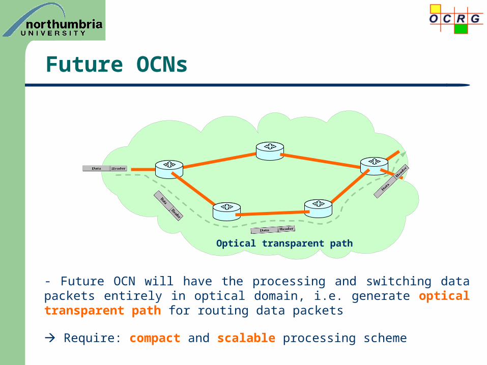
Future OCNs
Optical transparent path
- Future OCN will have the processing and switching data packets entirely in optical domain, i.e. generate optical transparent path for routing data packets
Require: compact and scalable processing scheme

Current All-optical Processing Schemes
All-optical logic gates All-optical correlators
Addresspatterns
Decimalvalue
Output ports
0 0 0 0 0 Port 2
0 0 0 1 1 Port 1
0 0 1 0 2 Port 3
0 0 1 1 3 Port 1
0 1 0 0 4 Port 3
0 1 0 1 5 Port 2
0 1 1 0 6 Port 2
0 1 1 1 7 Port 1
1 0 0 0 8 Port 3
1 0 0 1 9 Port 2
1 0 1 0 10 Port 2
1 0 1 1 11 Port 3
1 1 0 0 12 Port 1
1 1 0 1 13 Port 1
1 1 1 0 14 Port 2
1 1 1 1 15 Port 1
Routing table (R
T)
Example: N = 4, node with M = 3
?Port 1
Port 2
Port 3
N-bit
Problems:
• Large size routing table increased processing time• Optical device complexity poor scalability
Solution:
• To reduce the size of the routing table

PPM - Operation
Addressextraction
a0 a1 a2 a3payload
Header
(packet address)
Clk
Data packet
PPM(a) (b)
(a) (b)

PPM Based Routing Table
Grouping address patterns having the same output ports
Each new pulse-position routing table (PPRT) entry has optical pulses at the positions corresponding to the decimal values of group’s patterns
Pulse-position routing table (N = 4, M = 3)

Header Correlation
Single AND operation is required for matching PPM-address and multiple address patterns (PPRT entry)
Processing-time gain:
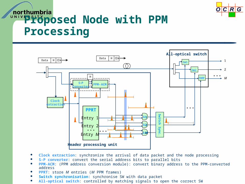
Proposed Node with PPM Processing
Clock extraction: synchronize the arrival of data packet and the node processing S-P converter: convert the serial address bits to parallel bits PPM-ACM: (PPM address conversion module): convert binary address to the PPM-converted address PPRT: store M entries (M PPM frames) Switch synchronisation: synchronise SW with data packet All-optical switch: controlled by matching signals to open the correct SW
Clock extraction
S-PConverter
PPM-ACM
&MM
SW1
SW2
SWM
Header processing unit
1
2
M
All-optical switch
...
...
...
...
Data H C lk
PPRT
Entry 1
Entry 2
Entry M ...
&11
&22
Sw
itch
Sy
nc.
Data H C lk
H

PPRT with Multimode Transmission
Same address pattern can appear at multiple PPRT entries
Modes: unicast, multicast, broadcast and deletion
Pulse-position routing table (N = 4, M = 3)

Node with Multicast Tx Mode
Clock extraction
S-PConverter
PPM-ACM
&MM
SW1
SW2
SWM
Header processing unit
1
2
M
All-optical switch
...
...
...
...
Data H C lk
PPRT
Entry 1
Entry 2
Entry M ...
&11
&22
Sw
itch
Sy
nc.
Data H C lk
H
Data H C lk

Optical PPM Generation Circuit
PPM-format address: y(t) = x(t + iai2iTs)
N-bit address-codeword: A = [ai {0,1}], i = 0, …, N–1

PPRT Generation
Is self-initialised with the extracted clock pulse. The M entries are filled by:
– Single optical pulse + Array of 2N optical delay lines; Or,
– M pattern generators + M optical modulators.

Ultrafast Optical AND Gate
A/B 0 1
0 0 0
1 0 1
Implementation:
Using optical interferometer configuration + optical nonlinear devices
A
BA×B
SOA1
SOA2
Symmetric Mach-Zehnder Interferometer (SMZI)

All-Optical Switch
1 MSMZ-1
SMZ-2
SMZ-M
…
CP1
CP2
CPM
1
2
M

Simulation Results
Simulation parametersSimulation parameters ValuesValues
Address length N 5
Number of outputs M 3
Bit rate 50 Gb/s
Payload 16 bits
Packet gap 2 ns
Pulse width FWHM 1 ps
Pulse’s power peak 2 mW
Wavelength 1554 nm
PPM slot duration Ts 5 ps
For an all-optical core network up to 25 = 32 nodes
... 32 node network
0
1
17
29
8
15 00000
0001
10001
01000
11101
01111

Simulation Results
Demonstrate the PPM processing and Tx modes
PPRT with 3 entries:

Simulation Results
Input
Output 1
Output 2
Output 3

Simulation Results
0 1 1 1 0Packet with address 01110
PPM-converted address
PPRT entry 1
Synchronized matching pulse

Conclusions
PPM processing scheme– Reduces the required processing time– Provides the scalability: adding/dropping network nodes
and node outputs
Applications: – All-optical core/backbone networks (N >> M ~ 3-6)– Optical bypass router (electrical router + optical bypass
router)
Challenges: – Optical switch with long and variable switching window– Timing jitter and received pulse dispersion

Publications
H. Le-Minh, Z. Ghassemlooy, and W. P. Ng., “A novel node architecture for all-optical packet switched network”, proceeding of 10th European Conference on Networks and Optical Communications 2005 (NOC2005), pp. 209-216, London, UK, Jul. 2005
H. Le-Minh, Z. Ghassemlooy, and W. P. Ng., ”Ultrafast header processing in all-optical packet switched-network” proceeding of 7th International Conference on Transparent Optical Networks 2005 (ICTON2005), Vol. 2, pp. 50-53, Barcelona, Spain, Jul. 2005

Acknowledgements
Northumbria University for sponsoring the research work

Thank you!