Embed Size (px)
Citation preview

All-semiconductor active plasmonic system in mid-infrared wavelengths
Debin Li and C. Z. Ning*
School of Electrical, Computer and Energy Engineering, Arizona State University, Tempe, Arizona 85287, USA *[email protected]
Abstract: Metal-based plasmonics has a wide range of important applications but is subject to several drawbacks. In this paper, we propose and investigate an all-semiconductor-based approach to plasmonics in mid-infrared (MIR) wavelength range using InAs heterostructures. Our results show that InAs heterostructures are ideal for plasmonics with the shortest plasmon wavelength among common semiconductors. More importantly, as we will show, InAs heterostructures are superior to metal-based plasmonics for MIR applications due to much reduced loss, improved confinement, and ease of tunability of resonant wavelengths through carrier density. Finally, we propose and investigate a monolithic all-semiconductor integrated active plasmonic system with active source, waveguide, and detector all integrated on a chip, realizable in a single epitaxial growth process. Such an all semiconductor based system can be advantageous not only in plasmonics, but also in active metamaterials.
©2011 Optical Society of America
OCIS codes: (250.5403) Plasmonics; (130.6750) Systems; (230.7370) Waveguides.
References and links
1. H. A. Atwater, “The promise of plasmonics,” Sci. Am. 296(4), 56–62 (2007). 2. S. Maier, Plasmonics: Fundamentals and Applications (Springer, 2007). 3. N. I. Zheludev, “Applied physics. The road ahead for metamaterials,” Science 328(5978), 582–583 (2010). 4. J. Valentine, S. Zhang, T. Zentgraf, E. Ulin-Avila, D. A. Genov, G. Bartal, and X. Zhang, “Three-dimensional
optical metamaterial with a negative refractive index,” Nature 455(7211), 376–379 (2008). 5. T. Okamoto, I. Yamaguchi, and T. Kobayashi, “Local plasmon sensor with gold colloid monolayers deposited
upon glass substrates,” Opt. Lett. 25(6), 372–374 (2000). 6. A. G. Brolo, R. Gordon, B. Leathem, and K. L. Kavanagh, “Surface plasmon sensor based on the enhanced light
transmission through arrays of nanoholes in gold films,” Langmuir 20(12), 4813–4815 (2004). 7. A. V. Maslov and C. Z. Ning, “Size reduction of a semiconductor nanowire laser by using metal coating,” Proc.
SPIE 6468, 646801 (2007). 8. M. Hill, Y.-S. Oei, B. Smalbrugge, Y. Zhu, T. de Vries, P. J. van Veldhoven, F. W. M. van Otten, T. J.
Eijkemans, J. P. Turkiewicz, H. de Waardt, E. J. Geluk, S.-H. Kwon, Y.-H. Lee, R. Nötzel, and M. K. Smit, “Lasing in metallic-coated nanocavities,” Nat. Photonics 1(10), 589–594 (2007).
9. M. T. Hill, M. Marell, E. S. P. Leong, B. Smalbrugge, Y. Zhu, M. Sun, P. J. van Veldhoven, E. J. Geluk, F. Karouta, Y.-S. Oei, R. Nötzel, C. Z. Ning, and M. K. Smit, “Lasing in metal-insulator-metal sub-wavelength plasmonic waveguides,” Opt. Express 17(13), 11107–11112 (2009).
10. C. Z. Ning, “Semiconductor nanolasers,” Phys. Status Solidi 247, 774–788 (2010) (b). 11. M. A. Noginov, G. Zhu, A. M. Belgrave, R. Bakker, V. M. Shalaev, E. E. Narimanov, S. Stout, E. Herz, T.
Suteewong, and U. Wiesner, “Demonstration of a spaser-based nanolaser,” Nature 460(7259), 1110–1112 (2009).
12. R. F. Oulton, V. J. Sorger, T. Zentgraf, R.-M. Ma, C. Gladden, L. Dai, G. Bartal, and X. Zhang, “Plasmon lasers at deep subwavelength scale,” Nature 461(7264), 629–632 (2009).
13. H. T. Miyazaki and Y. Kurokawa, “Squeezing visible light waves into a 3-nm-thick and 55-nm-long plasmon cavity,” Phys. Rev. Lett. 96(9), 097401 (2006).
14. D. B. Li and C. Z. Ning, “Giant modal gain, amplified surface plasmon-polariton propagation, and slowing down of energy velocity in a metal-semiconductor-metal structure,” Phys. Rev. B 80(15), 153304 (2009).
15. D. B. Li and C. Z. Ning, “Peculiar features of confinement factors in a metal-semiconductor waveguide,” Appl. Phys. Lett. 96(18), 181109 (2010).
16. T. Ergin, N. Stenger, P. Brenner, J. B. Pendry, and M. Wegener, “Three-dimensional invisibility cloak at optical wavelengths,” Science 328(5976), 337–339 (2010).
#147367 - $15.00 USD Received 10 May 2011; revised 29 Jun 2011; accepted 3 Jul 2011; published 14 Jul 2011(C) 2011 OSA 18 July 2011 / Vol. 19, No. 15 / OPTICS EXPRESS 14594
17. A. J. Hoffman, L. Alekseyev, S. S. Howard, K. J. Franz, D. Wasserman, V. A. Podolskiy, E. E. Narimanov, D. L. Sivco, and C. Gmachl, “Negative refraction in semiconductor metamaterials,” Nat. Mater. 6(12), 946–950 (2007).
18. S. P. Burgos, R. de Waele, A. Polman, and H. A. Atwater, “A single-layer wide-angle negative-index metamaterial at visible frequencies,” Nat. Mater. 9(5), 407–412 (2010).
19. M. I. Stockman, “Spasers explained,” Nat. Photonics 2(6), 327–329 (2008). 20. R. Soref, “Mid-infrared photonics in silicon and germanium,” Nat. Photonics 4(8), 495–497 (2010). 21. R. Soref, R. E. Peale, and W. Buchwald, “Longwave plasmonics on doped silicon and silicides,” Opt. Express
16(9), 6507–6514 (2008). 22. S. Adachi, “Model dielectric constants of GaP, GaAs, GaSb, InP, InAs, and InSb,” Phys. Rev. B Condens. Matter
35(14), 7454–7463 (1987). 23. E. Burstein, “Anomalous optical absorption limit in InSb,” Phys. Rev. 93(3), 632–633 (1954). 24. H. Kroemer, “The 6.1 Å family (InAs, GaSb, AlSb) and its heterostructures: a selective review,” Physica E 20(3-
4), 196–203 (2004). 25. D. C. Larrabee, G. A. Khodaparast, J. Kono, K. Ueda, Y. Nakajima, M. Nakai, S. Sasa, M. Inoue, K. I.
Kolokolov, J. Li, and C. Z. Ning, “Temperature dependence of intersubband transitions in InAs/AlSb quantum wells,” Appl. Phys. Lett. 83(19), 3936–3938 (2003).
26. J. Li, K. I. Kolokolov, C. Z. Ning, D. C. Larrabee, G. A. Khodaparast, J. Kono, K. Ueda, Y. Nakajima, S. Sasa, and M. Inoue, “Intersubband transitions in InAs/AlSb quantum wells,” in Progress in Semiconductors II: Electronic and Optoelectronic Applications, MRS Proceedings (2003), Vol. 744, p. 571.
27. K. Kolokolov and C. Z. Ning, “Doping induced type-II to type-I transition and interband optical gain in InAs/AlSb quantum wells,” Appl. Phys. Lett. 83(8), 1581–1583 (2003).
28. www.silvaco.com. 29. J. D. Jackson, Classical Electrodynamics, 3rd ed. (Wiley, 1999). 30. G. W. Ford and W. H. Weber, “Electromagnetic interactions of molecules with metal surfaces,” Phys. Rep.
113(4), 195–287 (1984). 31. www.comsol.com.
1. Introduction
Plasmonics [1,2] and metamaterials [3,4] have impacted many fields of research such as detecting and sensing [5,6], nanolasers and spasers [7–12], sub-wavelength confinement [13–15], optical cloaking [16], and other applications [17–19]. However, great challenges remain to fully realize many promised potentials, as we describe in the following. First, common metals such as gold or silver have plasmon resonances in blue or deep ultra-violate wavelength ranges. There are no available metals whose plasmon resonances are in the near or mid-infrared (MIR) wavelength range (say from 1 to 10 microns), which is an extremely important wavelength range for detection and sensing [20,21]. Second, it is highly desirable for many applications to integrate plasmonic structures with gain materials or with other dielectric materials. These applications include active metamaterials or active plasmonic system containing gain sections. But there is an intrinsic incompatibility of low-quality metal deposition with high-quality epitaxial growth of semiconductors or dielectrics. As a result, many intrinsic plasmonic properties can be masked by the poor metal quality or poor semiconductor-metal interfaces. Third, large metal loss is still a key problem for many plasmonic and metamaterial applications. In addition, the plasmonic resonance frequency (or wavelength) is fixed for a given metal. There is no tunability that could benefit many applications. Thus it is important for plasmonic applications to look into other alternatives to metals such as highly doped semiconductors.
While metallic properties of highly doped semiconductors have been used in longer wavelengths [17,20,21], their applications in shorter MIR wavelengths have not been explored. Here we demonstrate an all-semiconductor plasmonics that overcomes these challenges by using InAs heterostructures which offer the shortest plasmon wavelengths among common semiconductors with wide tunability. As we will show, the plasmonic properties of InAs-based heterostructures are superior to those of metals with much reduced optical loss and much improved modal confinement or field enhancement. Furthermore we propose and study a prototype of a monolithic all-semiconductor active plasmonic system including source, active waveguide, and detector, all realizable on a chip in a single epitaxial growth process. We believe that such metal-free plasmonic systems will have profound impact to all above applications.
#147367 - $15.00 USD Received 10 May 2011; revised 29 Jun 2011; accepted 3 Jul 2011; published 14 Jul 2011(C) 2011 OSA 18 July 2011 / Vol. 19, No. 15 / OPTICS EXPRESS 14595

2. Interband and intraband transitions in a semiconductor
For a semiconductor with high electron density, it is important to include both interband and intraband transitions, especially for narrow gap semiconductors. The relationship between electric displacement vector D and electric field E can be written as:
0 b e D E P P (1)
where 0 is the permittivity in vacuum, Pb and Pe are the polarizations for the interband
transitions and intraband transitions (or free electrons), respectively. The free electron
polarization is related to the electric field E through the linear susceptibility, e , according
to0e e P E .
e can be approximated by the Drude model:
22
2 2
0
( )( / ) /
p
e
Ne
m i i
(2)
where N is the free electron concentration, e is the electron charge unit, m is the effective mass of electrons in semiconductor and is the free electron relaxation time. The plasmon
frequency p is given by
2
0
p
Ne
m
(3)
where is the semiconductor dielectric constant for p . The dielectric function
corresponding to the interband transitions is given by 1b b , which can be calculated
using a semi-empirical expression for undoped or lightly doped semiconductors [22]. This model used a multi-transition best fit to the experimentally measured dielectric function to get
b . Semiconductors with small effective mass in conduction band, such as InSb or InAs, are
easy to become degenerate at high electron density. In that case the absorption cannot happen near band edge since the bottom of conduction band is fully or nearly fully occupied by electrons, as was first noticed by Burstein [23]. The absorption coefficient, α, can be given by taking into account of the occupation probabilities of electrons and holes, fe and fh, respectively:
0 0[(1 )(1 ) ] (1 )e h e h e hf f f f f f (4)
where α0 is the absorption coefficient in undoped or lightly doped semiconductor. The absorption coefficient is related to the imaginary part of semiconductor dielectric constant by
/b bn c , where nb is the background refractive index and c is the speed of light in
vacuum. Finally the total dielectric constant is given as r b e .
3. Plasmonic features of InAs heterostructures
Carrier densities that can be introduced in common semiconductors are orders of magnitude lower than in metals, so that plasmon resonances in doped semiconductors are typically in wavelength range longer than 10 microns [17]. One of the key tasks for semiconductor plasmonics is to identify semiconductors and related heterostructures that can be highly doped or injected, such that the plasmon resonances can be in the MIR wavelength range. To compare the relative merits of common semiconductors, we plot in Fig. 1(a) the
corresponding plasmon wavelengths ( 2 /p pc ) as a function of electron density. As we
can see, InAs has the shortest plasmon wavelength for a given electron density. Even though all semiconductors can in principle be doped for plasmonic applications, the required doping
#147367 - $15.00 USD Received 10 May 2011; revised 29 Jun 2011; accepted 3 Jul 2011; published 14 Jul 2011(C) 2011 OSA 18 July 2011 / Vol. 19, No. 15 / OPTICS EXPRESS 14596
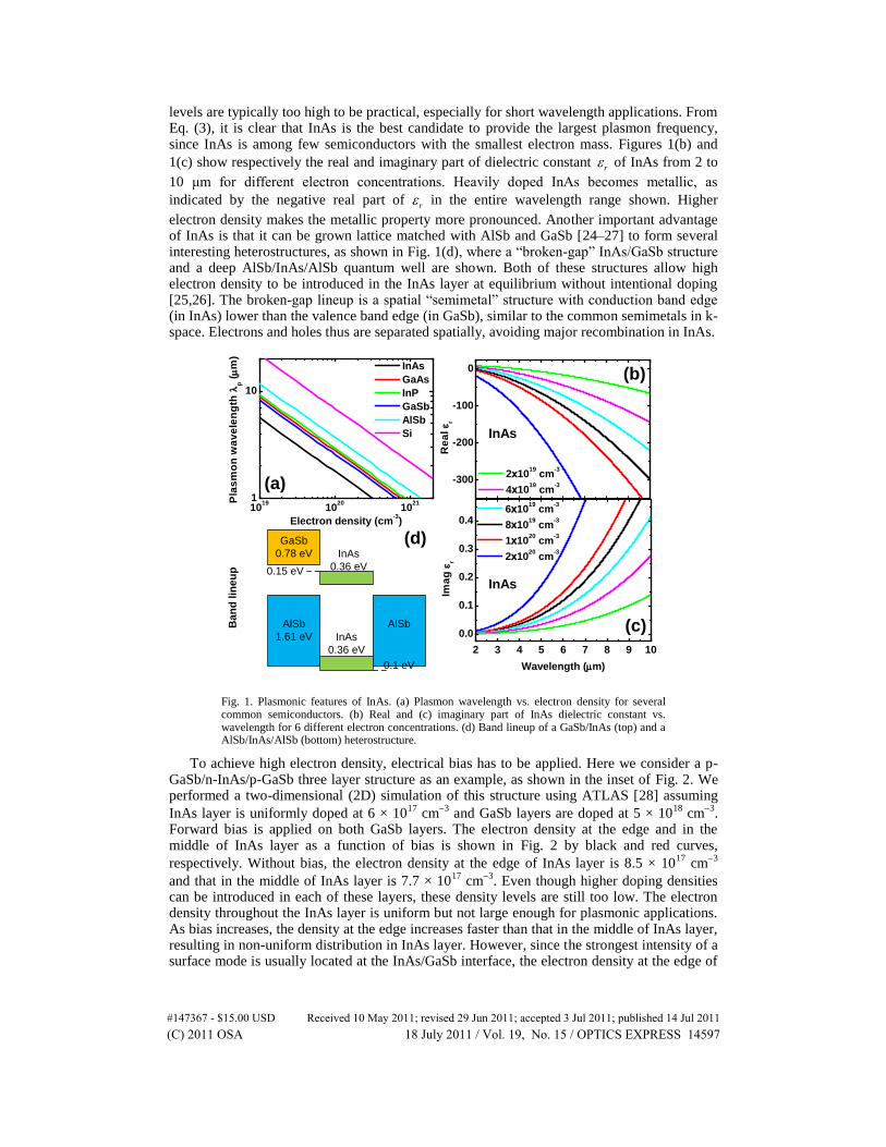
levels are typically too high to be practical, especially for short wavelength applications. From Eq. (3), it is clear that InAs is the best candidate to provide the largest plasmon frequency, since InAs is among few semiconductors with the smallest electron mass. Figures 1(b) and
1(c) show respectively the real and imaginary part of dielectric constant r of InAs from 2 to
10 μm for different electron concentrations. Heavily doped InAs becomes metallic, as
indicated by the negative real part of r in the entire wavelength range shown. Higher
electron density makes the metallic property more pronounced. Another important advantage of InAs is that it can be grown lattice matched with AlSb and GaSb [24–27] to form several interesting heterostructures, as shown in Fig. 1(d), where a “broken-gap” InAs/GaSb structure and a deep AlSb/InAs/AlSb quantum well are shown. Both of these structures allow high electron density to be introduced in the InAs layer at equilibrium without intentional doping [25,26]. The broken-gap lineup is a spatial “semimetal” structure with conduction band edge (in InAs) lower than the valence band edge (in GaSb), similar to the common semimetals in k-space. Electrons and holes thus are separated spatially, avoiding major recombination in InAs.
GaSb
0.78 eV
0.15 eV
Ba
nd
lin
eu
p
AlSb
1.61 eV
InAs
0.36 eV
InAs
0.36 eV
AlSb
0.1 eV
(a)
(b)
(c)
(d)
1019
1020
1021
1
10
2 3 4 5 6 7 8 9 10
0.0
0.1
0.2
0.3
0.4
InAs
6x10¹⁹
cm-3
8x10¹⁹
cm-3
1x10²⁰
cm-3
2x10²⁰
cm-3
Ima
g
r
Wavelength (m)
-300
-200
-100
0
2x10¹⁹
cm-3
4x10¹⁹
cm-3
Re
al r
InAs
InAs
GaAs
InP
GaSb
AlSb
Si
Pla
sm
on
wa
ve
len
gth
p (
m)
Electron density (cm-3)
Fig. 1. Plasmonic features of InAs. (a) Plasmon wavelength vs. electron density for several common semiconductors. (b) Real and (c) imaginary part of InAs dielectric constant vs. wavelength for 6 different electron concentrations. (d) Band lineup of a GaSb/InAs (top) and a AlSb/InAs/AlSb (bottom) heterostructure.
To achieve high electron density, electrical bias has to be applied. Here we consider a p-GaSb/n-InAs/p-GaSb three layer structure as an example, as shown in the inset of Fig. 2. We performed a two-dimensional (2D) simulation of this structure using ATLAS [28] assuming
InAs layer is uniformly doped at 6 × 10¹⁷
cm3
and GaSb layers are doped at 5 × 10¹⁸
cm3
. Forward bias is applied on both GaSb layers. The electron density at the edge and in the middle of InAs layer as a function of bias is shown in Fig. 2 by black and red curves,
respectively. Without bias, the electron density at the edge of InAs layer is 8.5 × 10¹⁷
cm3
and that in the middle of InAs layer is 7.7 × 10¹⁷
cm3
. Even though higher doping densities can be introduced in each of these layers, these density levels are still too low. The electron density throughout the InAs layer is uniform but not large enough for plasmonic applications. As bias increases, the density at the edge increases faster than that in the middle of InAs layer, resulting in non-uniform distribution in InAs layer. However, since the strongest intensity of a surface mode is usually located at the InAs/GaSb interface, the electron density at the edge of
#147367 - $15.00 USD Received 10 May 2011; revised 29 Jun 2011; accepted 3 Jul 2011; published 14 Jul 2011(C) 2011 OSA 18 July 2011 / Vol. 19, No. 15 / OPTICS EXPRESS 14597

InAs layer is more important for plasmonic application. We can see that the electron density
at the edge reaches 1 × 10²⁰
cm3
at a bias of 4 V, a large enough value for our plasmonic application.
0 1 2 3 4 5 6 7 8
1018
1019
1020
edge
middle
Ele
ctr
on
de
ns
ity
(c
m-3)
Bias (V)
p-GaSb
100nm
n-InAs
20nm
p-GaSb
100nm
Fig. 2. Electron density as a function of bias in a GaSb/InAs/GaSb structure (inset). The black and red curves show respectively the electron density at the edge and in the middle of InAs layer. The thickness of each layer in the GaSb/InAs/GaSb structure is shown in the inset.
To demonstrate the advantages of plasmonic features of InAs structures, we consider a prototype surface plasmon polariton (SPP) structure: a bi-layer structure with a heavily doped
InAs layer (dielectric constant m ) as a metallic layer interfaced with a GaSb layer with a
dielectric constant s . Assume the SPP wave propagates along the InAs/GaSb interface in the
z direction, the propagation wavevector kz is given by / ( )z s m s mkc
. The quality
factor (Q factor) of this mode can be obtained via the definition [29]:
,2
stored
dissipated z E z
WQ
P k v
(5)
where zk is the imaginary part of the propagation wavevector and ,E zv is the average energy
velocity of the mode [14]. Figure 3 shows the Q factors as a function of wavelength of a SPP mode in an InAs/GaSb structure with different electron concentrations, in an Ag/GaSb structure, and in an Au/GaSb structure. The dip (minimum) in each curve corresponds to the SPP resonance. We can see that the Q-factor of InAs/GaSb structure increases with electron density on the longer wavelength side of plasmon resonance. The situation becomes more complicated below plasmon resonance wavelength. One important result is that the Q factor of InAs/GaSb structure is several times larger than that of Ag/GaSb and Au/GaSb structures. Therefore, highly doped InAs structure is an excellent plasmonic waveguide and is superior to typical metal-based structures.
#147367 - $15.00 USD Received 10 May 2011; revised 29 Jun 2011; accepted 3 Jul 2011; published 14 Jul 2011(C) 2011 OSA 18 July 2011 / Vol. 19, No. 15 / OPTICS EXPRESS 14598

2 3 4 5 6 7 8 9 1010
2
103
104
2x10¹⁹
4x10¹⁹
8x10¹⁹
1x10202x10
20cm
-3
6x10¹⁹
Au/GaSbAg/GaSb
InAs/GaSb
Q f
ac
tor
Wavelength (m)
Fig. 3. Quality factors vs. wavelength of a SPP mode in an InAs/GaSb structure with different
electron concentrations (cm3), in an Ag/GaSb structure, and in an Au/GaSb structure.
It is interesting to see how tightly a mode can be bound at the InAs/GaSb interface, since tight confinement of a mode is important for nanophotonic applications. Figure 4 shows normalized energy density and power flux (absolute value) profile across the interface of the InAs/GaSb structure for different electron concentrations in InAs at 3 and 5 μm, respectively. We can see from Figs. 4(a) and 4(b) that the energy and power densities for InAs/GaSb at
electron density 6 × 10¹⁹
cm3
are almost flat in both InAs and GaSb layers. This is because the working wavelength is shorter than the SPP resonance wavelength so that SPP mode is very loosely bound at the interface. The situation is the same for the case with density 2 × 10
19
cm3
in Figs. 4(c) and 4(d). The operating wavelength thus has to be longer than the SPP wavelength for better SPP localization. In order to quantitatively describe the mode confinement at the interface, we introduce effective widths (Wt) across the interface as the sum of the width in InAs layer, Wm, and that in GaSb layer, Ws (see Figs. 4(a) and 4(b)). They
are defined as the distance from the interface through which the energy or power decays to e2
of their values at the interface. The three widths measured at the working wavelength of 3 μm
are listed in Table 1. The effective widths for InAs/GaSb waveguide at density 6 × 10¹⁹
cm3
are extremely long, corresponding to the flat curve in Figs. 4(a) and 4(b). For larger electron
density, the effective widths are small. The total effective width at density 8 × 10¹⁹
cm3
is the smallest one, because the working wavelength is very close to but still longer than the SPP resonance wavelength where the SPP mode has the best confinement. The total effective width at 73 nm is one fortieth of the working wavelength in this case, representing a huge compression of the effective wavelength. There are similar conclusions for the case with working wavelength at 5 μm, with the required density somewhat smaller. Since the Q factor at the SPP resonance is the smallest (see Fig. 3), the electron density in InAs needs to be well controlled to meet the requirement of both quality and confinement in a waveguide design.
Table 1. Effective Widths in InAs/GaSb Structure at 3 μm
Electron density (cm3) 6 × 10¹⁹ 8 × 10¹⁹ 1 × 10²⁰ 2 × 10²⁰
Ws (nm) >104 38 95 218 Wm (nm) >104 35 60 54 Wt (nm) >2 × 10⁴ 73 155 272
#147367 - $15.00 USD Received 10 May 2011; revised 29 Jun 2011; accepted 3 Jul 2011; published 14 Jul 2011(C) 2011 OSA 18 July 2011 / Vol. 19, No. 15 / OPTICS EXPRESS 14599

-100 -75 -50 -25 0 25 50 75 1000.0
0.2
0.4
0.6
0.8
1.0
(b)
Ws
Wm
Norm
alize
d p
ow
er
flux
(absolu
te v
alu
e)
Distance vertical to the interface (nm)
0.0
0.2
0.4
0.6
0.8
1.0
(a)
6x10¹⁹
cm-3
8x10¹⁹
cm-3
1x10²⁰
cm-3
2x10²⁰
cm-3
GaSbInAs
Norm
alize
d e
nerg
y
density
-100 -75 -50 -25 0 25 50 75 100
(d)
(c)
8x10¹⁹
cm-3
6x10¹⁹
cm-3
4x10¹⁹
cm-3
2x10¹⁹
cm-3
wavelength at 3 m wavelength at 5 m
Fig. 4. (a) Normalized energy density and (b) power flux (absolute value) profile across the interface of an InAs/GaSb structure at 3 μm. The effective widths in InAs layer, Wm, and in GaSb layer, Ws, are schematically shown as well. (c) Normalized energy density and (d) power flux (absolute value) profile at 5 μm.
4. All-semiconductor plasmonic system
The most interesting aspect of an all-semiconductor plasmonic structure is the possibility of monolithically growing an entire plasmonic system with various components on a chip. To illustrate this exciting aspect, we propose and conduct a design study of an all-semiconductor plasmonic system consisting of a SPP source, a waveguide with integrated amplifiers, and a detector, as shown in Fig. 5(a). All three components can be grown in a single epitaxial growth process and each component can be then defined lithographically. The high electron
density (on the order of 1020
cm3
) in InAs can be achieved by electrical bias of the doped structures. An active structure is needed to provide gain in the source and amplifier. In addition to InAs and GaSb, AlSb can be used as a barrier material. The layer structures of all three components are identical and shown in Fig. 5(b) where the material composition, doping types, thickness and polarity of electrodes of each layer are also shown. The active region consists of p-AlSb/i-InAs/n-AlSb triple layers, with the intrinsic InAs layer serving as the gain layer. This structure has been shown to be able to produce strong interband gain despite being a type-II structure for the undoped system [27]. The plasmonic structure consists of p-GaSb/n-InAs/p-GaSb triple layers. SPP mode is formed and propagating at the two n-InAs/p-GaSb interfaces, as we studied above in Section 3. The overall working principle of this system is illustrated in Fig. 5(c).
Source: The bias V1 is positive in the source, electrons and holes are thus injected into the i-InAs layer. Optical dipoles formed by the electron-hole pairs in this layer then recombine to excite and transfer energy preferentially to the SPP mode at the two p-GaSb/n-InAs interfaces [30]. The SPPs are thus generated in the source. If a time-varying signal voltage VS(t) is added to V1, the amplitude of the SPPs will be modulated according to the strength of the signal.
Amplifier: The amplifier functions similar to the source. The bias V1 has the same positive constant value V0 as that in the source. When passing through the amplifier, the SPPs from source will acquire energy emitted from the electron-hole pairs in the i-InAs layer and get amplified.
Detector: The bias V1 in the detector is negative, so the i-InAs layer is depleted. The incoming SPPs are then absorbed by InAs layers of the detector. The portion of the energy absorbed by the i-InAs initiates the generation of the electrons and holes in this layer which
#147367 - $15.00 USD Received 10 May 2011; revised 29 Jun 2011; accepted 3 Jul 2011; published 14 Jul 2011(C) 2011 OSA 18 July 2011 / Vol. 19, No. 15 / OPTICS EXPRESS 14600

can be collected through the electrodes of the reversely biased p-i-n structure. Since the density of generated carriers is proportional to the amplitude of the arrived SPPs, the signal from the source is demodulated and detected by the detector. Note that the gain spectrum provided by the active region has a peak frequency larger than InAs bandgap, as shown earlier [27]. Therefore, most of the energy of the SPP mode can be absorbed by the InAs layer in the detector.
Source Detector
Waveguide
Amplifier
V1=-V0
V2
V2
Amplifier
V1=V0+Vs(t) V1=V0 V1=V0
Substrate
Source Detector
Waveguide
Amplifier
(a)
p-AlSb 50nm +
i-InAs 20nm
n-AlSb 10nm -p-GaSb 10nm +
n-InAs 20nm -
p-GaSb 50nm +
V1
V2
V2
z
x
(b)
(c)
SPP
Fig. 5. All-semiconductor active plasmonic system. (a) Schematic of the proposed plasmonic system consisting of a SPP source, a waveguide with amplifiers and a detector. (b) The layer structures of all three components of this system. The material composition, doping type, thickness and polarity of electrodes of each layer are also shown. (c) Illustration of the working principle of the system.
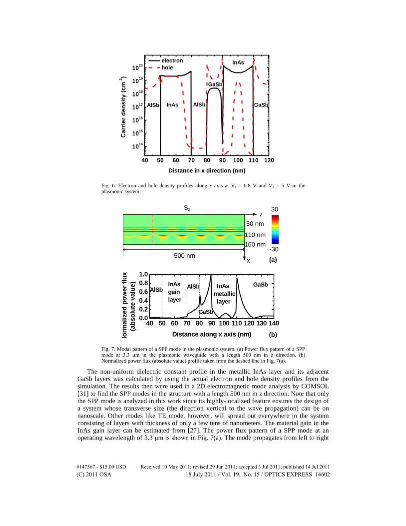
We performed a 2D simulation of this system using ATLAS assuming the layers in the
active structure are uniformly doped at 2.5 × 10¹⁸
cm3
and the layers in the plasmonic
structure are doped at 5 × 10¹⁸
cm3
. The electron and hole densities were calculated at V1 = 0.8 V (source and amplifier) and V2 = 5 V, and their profiles are shown in Fig. 6. The metallic InAs layer is located from x = 90 to 110 nm. At the edge of this layer, the maximum electron
density is about 1.5 × 10²⁰
cm3
while the hole density is lower than 1 × 10¹⁴
cm3
. This situation is exactly what we need for the InAs application as a metal. In the middle of the
metallic InAs layer (x = 100 nm), the minimum electron density is about 4.2 × 10¹⁹
cm3
, ensuring the maximum real part of the dielectric constant of InAs is still negative in the layer. Therefore this InAs layer can be treated as a pure metallic layer. Note that the hole density at the edge of GaSb layer is higher than the electron density at the edge of InAs layer, the metallic property of GaSb due to hole absorption thus needs to be considered. The collective motion of high-density holes can also be approximated by Drude model and the treatment of dielectric function of GaSb is similar to that shown in Section 2 for InAs. The InAs gain layer is located from x = 50 to 70 nm. The carrier density on the right half of this layer is not uniform because holes are preferentially swept from the middle AlSb layer into the GaSb layer on the right instead into the InAs layer on the left, leading to low hole density on the right half of InAs gain layer. The carrier density is, however, high and uniform enough on the left half of this InAs layer, which can still provide high material gain to the whole system.
#147367 - $15.00 USD Received 10 May 2011; revised 29 Jun 2011; accepted 3 Jul 2011; published 14 Jul 2011(C) 2011 OSA 18 July 2011 / Vol. 19, No. 15 / OPTICS EXPRESS 14601
40 50 60 70 80 90 100 110 120
1014
1015
1016
1017
1018
1019
1020
electron
hole
GaSb
InAs
GaSb
AlSbInAsAlSb
Ca
rrie
r d
en
sit
y (
cm
-3)
Distance in x direction (nm)
Fig. 6. Electron and hole density profiles along x axis at V1 = 0.8 V and V2 = 5 V in the plasmonic system.
40 50 60 70 80 90 100 110 120 130 1400.0
0.2
0.4
0.6
0.8
1.0
No
rmalized
po
wer
flu
x
(ab
so
lute
valu
e)
Distance along x axis (nm)
AlSbInAs
gain
layer
AlSb
GaSb
GaSb InAs
metallic
layer
x
zSz
500 nm
50 nm
110 nm
160 nm
30
-30
(b)
(a)
Fig. 7. Modal pattern of a SPP mode in the plasmonic system. (a) Power flux pattern of a SPP mode at 3.3 μm in the plasmonic waveguide with a length 500 nm in z direction. (b) Normalized power flux (absolute value) profile taken from the dashed line in Fig. 7(a).
The non-uniform dielectric constant profile in the metallic InAs layer and its adjacent GaSb layers was calculated by using the actual electron and hole density profiles from the simulation. The results then were used in a 2D electromagnetic mode analysis by COMSOL [31] to find the SPP modes in the structure with a length 500 nm in z direction. Note that only the SPP mode is analyzed in this work since its highly-localized feature ensures the design of a system whose transverse size (the direction vertical to the wave propagation) can be on nanoscale. Other modes like TE mode, however, will spread out everywhere in the system consisting of layers with thickness of only a few tens of nanometers. The material gain in the InAs gain layer can be estimated from [27]. The power flux pattern of a SPP mode at an operating wavelength of 3.3 μm is shown in Fig. 7(a). The mode propagates from left to right
#147367 - $15.00 USD Received 10 May 2011; revised 29 Jun 2011; accepted 3 Jul 2011; published 14 Jul 2011(C) 2011 OSA 18 July 2011 / Vol. 19, No. 15 / OPTICS EXPRESS 14602

and increases exponentially due to the gain provided by the active structure. The normalized power flux (absolute value) profile taken at the location of the dashed line in Fig. 7(a) is shown in Fig. 7(b). We can see that most of the power of the structure travels outside the metallic InAs layer but is tightly bound at the InAs/GaSb interfaces. The effective width across the left-hand-side layers of the metallic InAs layer is about 26 nm. The propagation
length ( 1/ (2 )zk ) of the SPP mode in the waveguide without amplifier is below 10 μm.
However, since the amplifier provides the SPPs with a net modal gain ( 2 zk ) of 26.3 cm1
,
the SPPs can propagate over hundreds of microns if multiple-amplifier configuration is used. This structure is thus suitable for the nanoscale SPP waveguiding at 3.3 μm. The propagation length and the layout of the amplifiers required depend on the operating wavelength. To provide a gain at longer wavelengths, InAsSb alloy can be also used so that the operating wavelength can be somewhat further above the plasmon resonance wavelength of the InAs plasmonic structure.
5. Conclusion
In summary, we have investigated the plasmonic properties of InAs-heterostructures by using the Drude model. Our result showed that InAs-heterostructures are superior to other common semiconductors and metals for applications in plasmonic structures and metamaterials for MIR wavelengths. The SPP modal properties have been studied in detail using an InAs/GaSb bi-layer structure for different electron concentrations in the InAs layer. Finally, we proposed and studied a prototype system of a monolithic all-semiconductor integrated plasmonic system on a chip, realizable in a single epitaxial growth process. The significance and impact of the proposed plasmonic heterostructures and integrated system can be appreciated in several ways. First the InAs-based structures fill an important bandgap window between 2 and 8 microns for plasmonic applications in MIR range. While common metals can be used for MIR wavelength as good mirrors, but they cannot be used as plasmonic structures, since there is almost no localization near the metal surfaces at these long wavelengths. The easy tunability of plasmonic wavelength by simply changing the bias voltage is an important advantage of semiconductor based system. This allows a fabricated plasmonic system to be able to tune to different wavelength “on the fly”, a significant important feature for adaptable plasmonic system. The available semiconductors such as GaSb and AlSb that are lattice matched to InAs can work as barrier materials or allow easy design of active source, amplifying waveguide, and detector, all based on the same substrate. Thus an entire plasmonic system can be grown in a single epi-process. This is a significant advantage compared to plasmonic or metamaterial structures that use a combination of metals and semiconductors, since high quality semiconductors have to be grown epitaxially, while metals are typically deposited in a thermal process with much poorer crystal quality. Our all-epitaxially grown integrated plasmonic system in a single process can offer unprecedented quality and reliability. The low loss (or high quality factor) of InAs is another important advantage. Such metal-free, all-epi-growth approaches are especially important for metamaterials where more complicated structures on deep-subwavelength scales with higher fabrication precision are required. In addition, active gain materials can be integrated with the same epitaxial growth. All these remarkable features will make the proposed all-semiconductor active plasmonic system the most promising ones for tunable applications in MIR range. We believe that such all-semiconductor plasmonic systems will have a profound impact to many applications mentioned in this paper.
Acknowledgments
This work was supported by the Defense Advanced Research Project Agency (DARPA) program Nanoscale Architectures of Coherent Hyper-Optical Sources (NACHOS).
#147367 - $15.00 USD Received 10 May 2011; revised 29 Jun 2011; accepted 3 Jul 2011; published 14 Jul 2011(C) 2011 OSA 18 July 2011 / Vol. 19, No. 15 / OPTICS EXPRESS 14603