Embed Size (px)
Citation preview
All Shore Industries, Inc. One Edgewater Plaza, Staten Island, NY 10305
ALL SHORE INDUSTRIES, INC.
SPECIFICATION FOR LIQUID CRYSTAL DISPLAY MODULE
MODEL #: ASI-_-204CS-KJ-_YD/X
Number of Characters: ……………. 20 characters x 4 Lines
Module dimension: ……………….. 146.0 x 62.5 x 13.6(MAX)
View area: ………………………… 123.5 x 43.0
Active are: ………………………… 118.84x 38.47
Dot size: ………………………….. 0.92 x 1.1
Dot pitch: ………………………… 0.98 x 1.16
Character size: …………………… 4.84 x 9.22
Character pitch: …………………. 6.0 x 9.75
LCD type: ………………………. STN, Positive, Transflective, Yellow Green, Gray
Duty: ……………………………. 1/16
View direction: ………………….. 6 or 12 o’clock
Backlight Type: …………………. LED Yellow Green
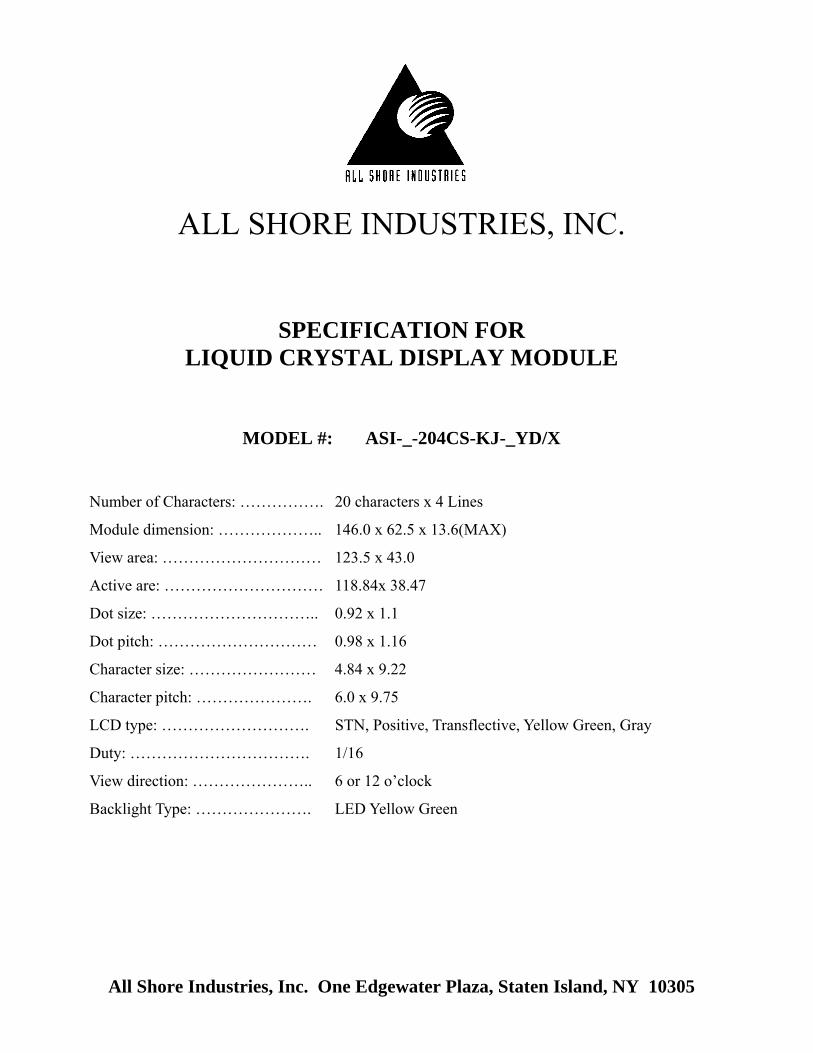
Version 1 Page 2
MODEL NO : ASI-_-204CS-KJ-_YD/X
All Shore Industries, Inc. One Edgewater Plaza, Staten Island, NY 10305 http://www.allshore.com/pdf/ASI_204CSKJ_YDX.pdf
Contents General Specification Absolute Maximum Ratings Electrical Characteristics Optical Characteristics Interface Pin Function Contour Drawing & Block Diagram Function Description Character Generator ROM Pattern Instruction Table Timing Characteristics Initializing of LCM Quality Assurance Reliability Backlight Information
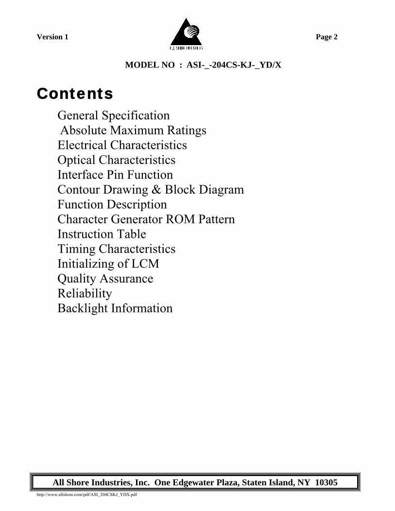
Version 1 Page 3
MODEL NO : ASI-_-204CS-KJ-_YD/X
All Shore Industries, Inc. One Edgewater Plaza, Staten Island, NY 10305 http://www.allshore.com/pdf/ASI_204CSKJ_YDX.pdf
Version 1 Page 4
MODEL NO : ASI-_-204CS-KJ-_YD/X
All Shore Industries, Inc. One Edgewater Plaza, Staten Island, NY 10305 http://www.allshore.com/pdf/ASI_204CSKJ_YDX.pdf
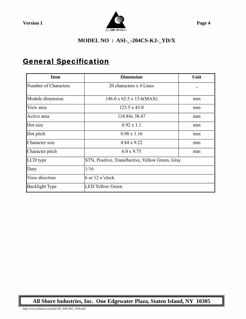
General Specification
Item Dimension Unit
Number of Characters 20 characters x 4 Lines -
Module dimension 146.0 x 62.5 x 13.6(MAX) mm
View area 123.5 x 43.0 mm
Active area 118.84x 38.47 mm
Dot size 0.92 x 1.1 mm
Dot pitch 0.98 x 1.16 mm
Character size 4.84 x 9.22 mm
Character pitch 6.0 x 9.75 mm
LCD type STN, Positive, Transflective, Yellow Green, Gray
Duty 1/16
View direction 6 or 12 o’clock
Backlight Type LED Yellow Green
Version 1 Page 5
MODEL NO : ASI-_-204CS-KJ-_YD/X
All Shore Industries, Inc. One Edgewater Plaza, Staten Island, NY 10305 http://www.allshore.com/pdf/ASI_204CSKJ_YDX.pdf
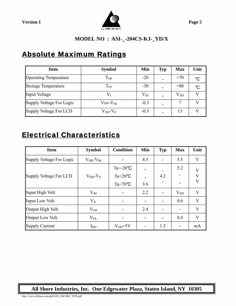
Absolute Maximum Ratings
Item Symbol Min Typ Max Unit
Operating Temperature TOP -20 - +70 ℃ Storage Temperature TST -30 - +80 ℃ Input Voltage VI VSS - VDD V
Supply Voltage For Logic VDD-VSS -0.3 - 7 V
Supply Voltage For LCD VDD-V0 -0.3 - 13 V
Electrical Characteristics
Item Symbol Condition Min Typ Max Unit
Supply Voltage For Logic VDD-VSS - 4.5 - 5.5 V
Supply Voltage For LCD VDD-V0
Ta=-20℃
Ta=20℃
Ta=70℃
-
- 3.6
- 4.2 -
5.2 -
-
V V V
Input High Volt. VIH - 2.2 - VDD V
Input Low Volt. VIL - - - 0.6 V
Output High Volt. VOH - 2.4 - - V
Output Low Volt. VOL - - - 0.4 V
Supply Current IDD VDD=5V - 1.5 - mA
Version 1 Page 6
MODEL NO : ASI-_-204CS-KJ-_YD/X
All Shore Industries, Inc. One Edgewater Plaza, Staten Island, NY 10305 http://www.allshore.com/pdf/ASI_204CSKJ_YDX.pdf
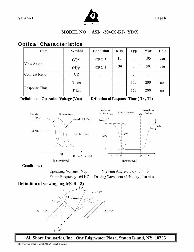
Optical Characteristics Item Symbol Condition Min Typ Max Unit
(V)θ CR≧ 2 10 - 105 deg View Angle
(H)φ CR≧ 2 -30 - 30 deg
Contrast Ratio CR - - 3 - -
T rise - - 150 200 ms Response Time T fall - - 150 200 ms
Definition of Operation Voltage (Vop) Definition of Response Time ( Tr , Tf )
Driving Voltage(V)
Intensity
Cr Max
100%
Vop
Selected Wave
Non-selected Wave
[positive type]
Cr = Lon / Loff
Intensity
90%100%
Tr
10%
Tf
Non-selectedConition
Non-selectedConitionSelected Conition
[positive type] Conditions : Operating Voltage : Vop Viewing Angle(θ,φ) : 0°, 0° Frame Frequency : 64 HZ Driving Waveform : 1/N duty , 1/a bias
Definition of viewing angle(CR�2)
θ fφ = 180°
φ = 90°
φ = 0°
φ = 270°
θ b
θ rθ l
Version 1 Page 7
MODEL NO : ASI-_-204CS-KJ-_YD/X
All Shore Industries, Inc. One Edgewater Plaza, Staten Island, NY 10305 http://www.allshore.com/pdf/ASI_204CSKJ_YDX.pdf
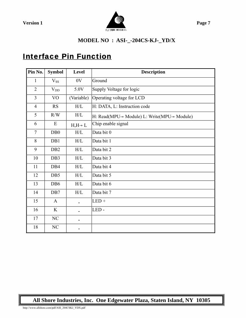
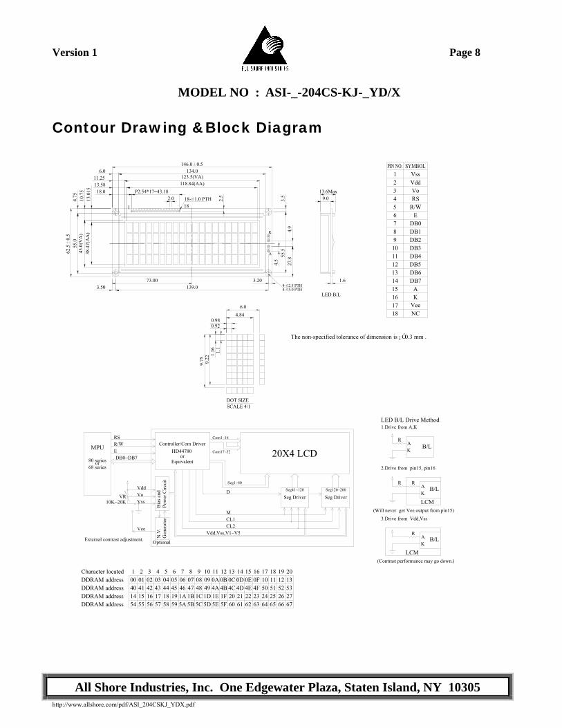
Interface Pin Function
Pin No. Symbol Level Description
1 VSS 0V Ground
2 VDD 5.0V Supply Voltage for logic
3 VO (Variable) Operating voltage for LCD
4 RS H/L H: DATA, L: Instruction code
5 R/W H/L H: Read(MPU→ Module) L: Write(MPU→ Module) 6 E H,H→ L Chip enable signal
7 DB0 H/L Data bit 0
8 DB1 H/L Data bit 1
9 DB2 H/L Data bit 2
10 DB3 H/L Data bit 3
11 DB4 H/L Data bit 4
12 DB5 H/L Data bit 5
13 DB6 H/L Data bit 6
14 DB7 H/L Data bit 7
15 A - LED +
16 K - LED -
17 NC -
18 NC -
Version 1 Page 8
MODEL NO : ASI-_-204CS-KJ-_YD/X
All Shore Industries, Inc. One Edgewater Plaza, Staten Island, NY 10305 http://www.allshore.com/pdf/ASI_204CSKJ_YDX.pdf
Contour Drawing &Block Diagram
The non-specified tolerance of dimension is ¡ Ó0.3 mm .
1.6
LED B/L
Seg DriverSeg120~200
123.5(VA)118.84(AA)
4.75
62.5
0.5
55.0
13.0
1510
.75
2.5
3.5
55.5
13.5811.25
134.06.0
68 series
44
58
Pow
er C
ircui
tG
ener
ator
OptionalExternal contrast adjustment.
1514 1716DDRAM addressDDRAM address 5554 56 57
N.V
.
Character located
DDRAM addressDDRAM address 01
41
20040
102 0342 43
3 4
10K~20K
Bia
s and
Vss
Vee
VddVoVR
232221201F1E1D1C1B1A1918 2524 26 275D5A59 5C5B 605E 5F 61 62 656463 6766
0949
10
Vdd,Vss,V1~V5
0646
04 0545
65 707 08
4847
8 90C4C
130A 0B4A 4B
11 120D 0E4D 4E
14 15
CL1CL2
M
Seg1~40
D
51
180F 1110
504F
171613125352
2019
Seg DriverSeg41~120
139.073.00
Controller/Com DriverRSR/W
DB0~DB7
MPU
80 seriesor
E
3.50
38.4
7(A
A)
43.0
(VA
)
9.75 9.22
1.16 1.
1
SCALE 4/1
HD44780
Equivalentor
Com17~32
Com1~16
DOT SIZE
20X4 LCD
6.04.84
3.20
0.920.98
4- 2.5 PTH4- 5.0 PTH
4.5
4.9
27.8
A
K
146.0 0.5
P2.54*17=43.1818.0
118- 1.0 PTH18
2.013.6Max
9.0
E6
2.Drive from pin15, pin16
B/L
3.Drive from Vdd,Vss
B/L
(Will never get Vee output from pin15)
(Contrast performance may go down.)LCM
AK
R
LCM
R RAK
LED B/L Drive Method
B/L
1.Drive from A,K
K
RA
18 NC
DB7
Vee17161514
KA
DB4
DB6DB5
DB3
13121110
DB289
7DB1DB0
2 Vdd
R/W45
3RSVo
Vss1
Version 1 Page 9
MODEL NO : ASI-_-204CS-KJ-_YD/X
All Shore Industries, Inc. One Edgewater Plaza, Staten Island, NY 10305 http://www.allshore.com/pdf/ASI_204CSKJ_YDX.pdf
Function Description
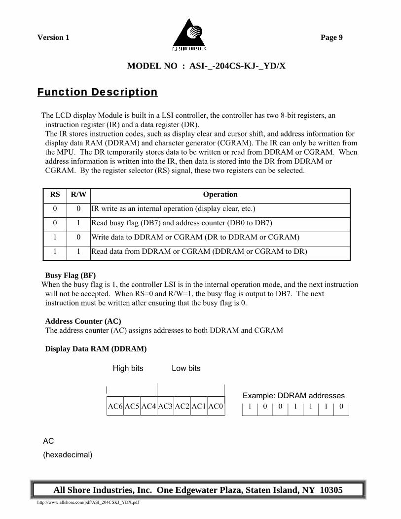
The LCD display Module is built in a LSI controller, the controller has two 8-bit registers, an instruction register (IR) and a data register (DR). The IR stores instruction codes, such as display clear and cursor shift, and address information for display data RAM (DDRAM) and character generator (CGRAM). The IR can only be written from the MPU. The DR temporarily stores data to be written or read from DDRAM or CGRAM. When address information is written into the IR, then data is stored into the DR from DDRAM or CGRAM. By the register selector (RS) signal, these two registers can be selected.
RS R/W Operation
0 0 IR write as an internal operation (display clear, etc.)
0 1 Read busy flag (DB7) and address counter (DB0 to DB7)
1 0 Write data to DDRAM or CGRAM (DR to DDRAM or CGRAM)
1 1 Read data from DDRAM or CGRAM (DDRAM or CGRAM to DR)
Busy Flag (BF)
When the busy flag is 1, the controller LSI is in the internal operation mode, and the next instruction will not be accepted. When RS=0 and R/W=1, the busy flag is output to DB7. The next instruction must be written after ensuring that the busy flag is 0.
Address Counter (AC) The address counter (AC) assigns addresses to both DDRAM and CGRAM Display Data RAM (DDRAM)
AC (hexadecimal)
High bits Low bits
AC6 AC5 AC4 AC3 AC2 AC1 AC0 1 0 0 1 1 1 0
Example: DDRAM addresses
Version 1 Page 10
MODEL NO : ASI-_-204CS-KJ-_YD/X
All Shore Industries, Inc. One Edgewater Plaza, Staten Island, NY 10305 http://www.allshore.com/pdf/ASI_204CSKJ_YDX.pdf
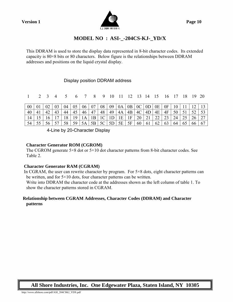
This DDRAM is used to store the display data represented in 8-bit character codes. Its extended capacity is 80×8 bits or 80 characters. Below figure is the relationships between DDRAM addresses and positions on the liquid crystal display.
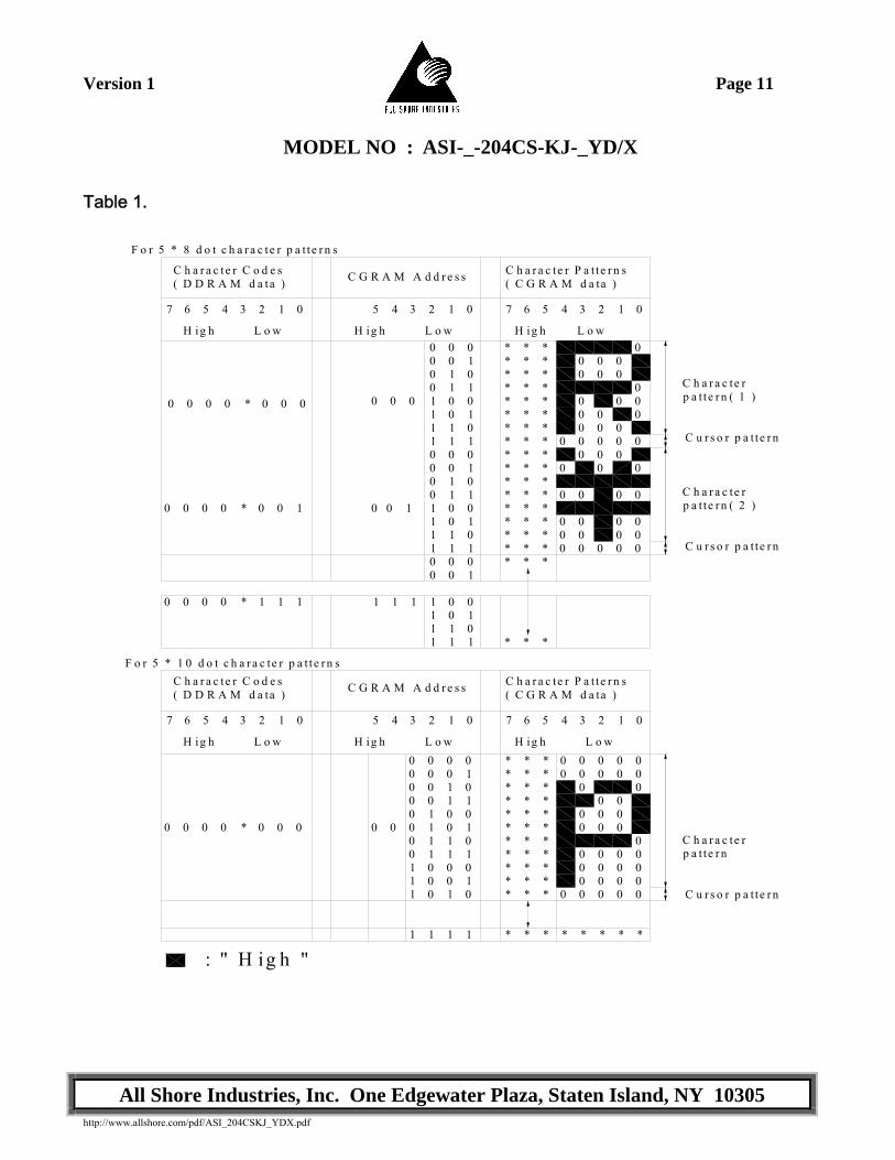
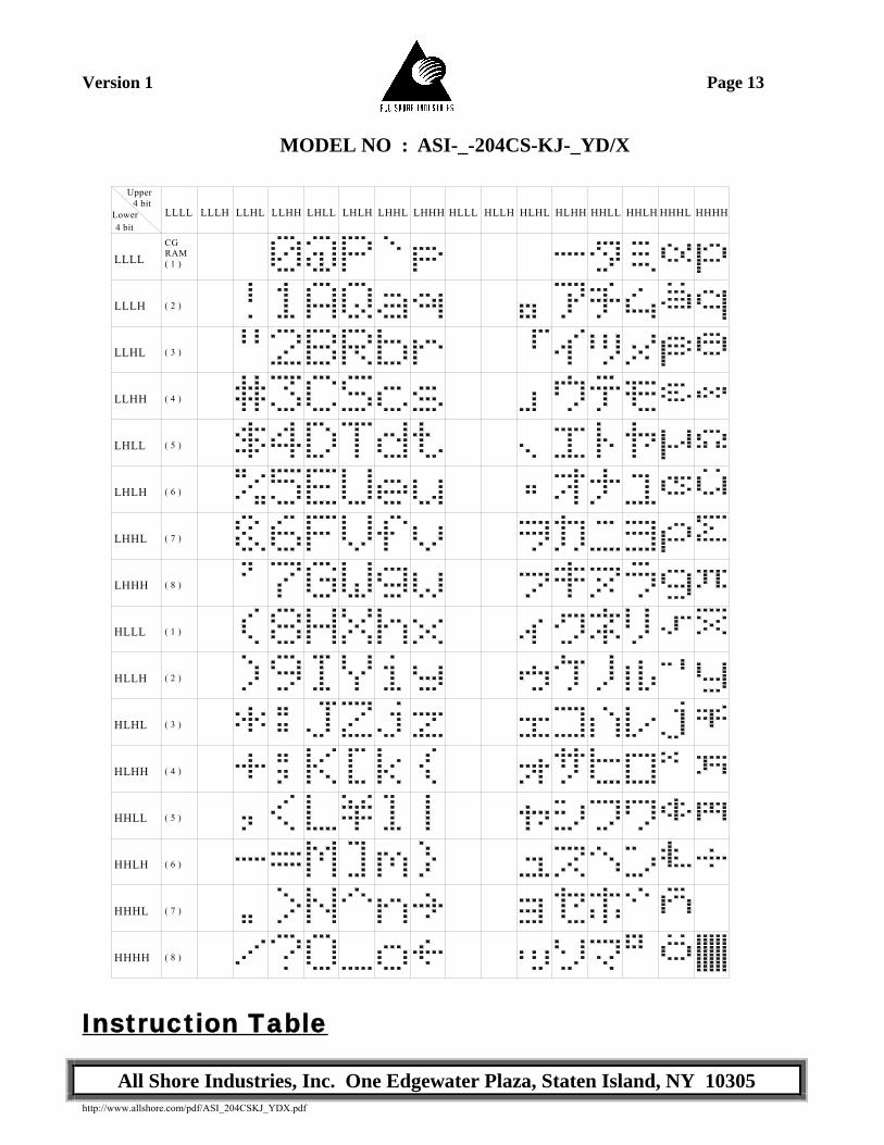
Character Generator ROM (CGROM) The CGROM generate 5×8 dot or 5×10 dot character patterns from 8-bit character codes. See Table 2.
Character Generator RAM (CGRAM) In CGRAM, the user can rewrite character by program. For 5×8 dots, eight character patterns can
be written, and for 5×10 dots, four character patterns can be written. Write into DDRAM the character code at the addresses shown as the left column of table 1. To show the character patterns stored in CGRAM.
Relationship between CGRAM Addresses, Character Codes (DDRAM) and Character
patterns
Display position DDRAM address
00 01 02 03 04 05 06 07 08 09 0A 0B 0C 0D 0E 0F 10 11 12 1340 41 42 43 44 45 46 47 48 49 4A 4B 4C 4D 4E 4F 50 51 52 5314 15 16 17 18 19 1A 1B 1C 1D 1E 1F 20 21 22 23 24 25 26 2754 55 56 57 58 59 5A 5B 5C 5D 5E 5F 60 61 62 63 64 65 66 67
4-Line by 20-Character Display
1 2 3 4 5 6 7 8 9 10 11 12 13 14 15 16 17 18 19 20
Version 1 Page 11
MODEL NO : ASI-_-204CS-KJ-_YD/X
All Shore Industries, Inc. One Edgewater Plaza, Staten Island, NY 10305 http://www.allshore.com/pdf/ASI_204CSKJ_YDX.pdf
Table 1.
F o r 5 * 8 d o t c h a r a c te r p a t t e r n s
C h a r a c te r C o d e s( D D R A M d a ta ) C G R A M A d d r e s s C h a r a c te r P a t t e r n s
( C G R A M d a ta )
5 4 3 2 1 067 5 4 3 2 01 7 6 5 4 3 2 1 0
0 0 000 110 010 101 001 111 011 100 000 110 010 101 001 111 011 100 000 1
01 001 111 011 1
* * ** * ** * ** * ** * ** * ** * ** * * 0 0 0 0 0* * ** * ** * ** * ** * ** * ** * ** * * 0 0 0 0 0
0 0 0 00 0 0 0
0 0 0 0
0 0 00 0 0
0 0 00 0 00 0 0
00 0 00 0 0
0
0 0 0
00 1
* * *
* * *
1 1 10 0 0 0 * 1 1 1
0 0 0 0 * 0 0 0
0 0 0 0 * 0 0 1
H ig h L o w H ig h L o w H ig h L o w
F o r 5 * 1 0 d o t c h a r a c te r p a t t e r n sC h a r a c te r C o d e s( D D R A M d a ta ) C G R A M A d d r e s s C h a r a c te r P a t t e r n s
( C G R A M d a ta )
7
H ig h L o w
456 3 2 1 0
H ig h L o w
5 4 3 2 1 0
H ig h L o w
7 6 5 4 123 0
* * * 0 0 0 0 00 0 0 0 0* * *
* * ** * ** * ** * ** * ** * ** * ** * ** * *
* * * * * * * *
0 0 0 00 0 0 10 0 1 00 0 1 10 1 0 00 1 0 10 1 1 00 1 1 11 0 0 01 0 0 11 0 1 0
1 1 1 1
0 0 0 0 0
0 0 0 0 * 0 0 0 0 0
0 00 0
0 0 00 0 0
00 0 0 00 0 0 00 0 0 0
C h a r a c te rp a t t e r n ( 1 )
C u r s o r p a t te r n
C h a r a c te rp a t t e r n ( 2 )
C u r s o r p a t te r n
C h a r a c te rp a t t e r n
C u r s o r p a t te r n
: " H ig h "
Version 1 Page 12
MODEL NO : ASI-_-204CS-KJ-_YD/X
All Shore Industries, Inc. One Edgewater Plaza, Staten Island, NY 10305 http://www.allshore.com/pdf/ASI_204CSKJ_YDX.pdf
Character Generator ROM Pattern
Version 1 Page 13
MODEL NO : ASI-_-204CS-KJ-_YD/X
All Shore Industries, Inc. One Edgewater Plaza, Staten Island, NY 10305 http://www.allshore.com/pdf/ASI_204CSKJ_YDX.pdf
LLLL LLLH LLHL LLHH LHLL LHLH LHHL LHHH HLLL HLLH HLHL HLHH HHLL HHLH HHHL
Upper4 bit
Lower4 bit
LLLL
LLLH
LLHL
LLHH
LHLL
LHLH
LHHL
LHHH
HLLL
HLLH
HLHL
HLHH
HHLL
HHLH
HHHL
HHHH
HHHH
CGRAM( 1 )
( 2 )
( 3 )
( 4 )
( 5 )
( 6 )
( 7 )
( 8 )
( 1 )
( 2 )
( 3 )
( 4 )
( 5 )
( 6 )
( 7 )
( 8 )
Instruction Table
Version 1 Page 14
MODEL NO : ASI-_-204CS-KJ-_YD/X
All Shore Industries, Inc. One Edgewater Plaza, Staten Island, NY 10305 http://www.allshore.com/pdf/ASI_204CSKJ_YDX.pdf
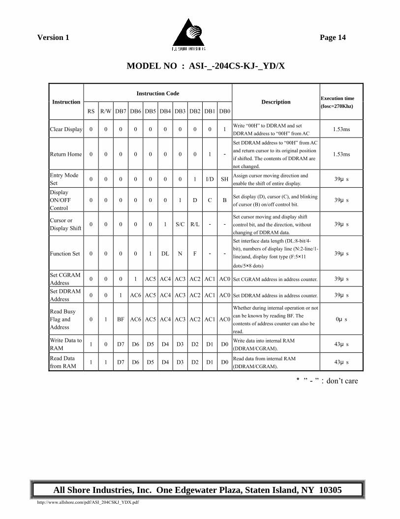
Instruction Code Instruction
RS R/W DB7 DB6 DB5 DB4 DB3 DB2 DB1 DB0Description Execution time
(fosc=270Khz)
Clear Display 0 0 0 0 0 0 0 0 0 1 Write “00H” to DDRAM and set DDRAM address to “00H” from AC
1.53ms
Return Home 0 0 0 0 0 0 0 0 1 -
Set DDRAM address to “00H” from AC and return cursor to its original position if shifted. The contents of DDRAM are not changed.
1.53ms
Entry Mode Set
0 0 0 0 0 0 0 1 I/D SH Assign cursor moving direction and enable the shift of entire display.
39μ s
Display ON/OFF Control
0 0 0 0 0 0 1 D C B Set display (D), cursor (C), and blinking of cursor (B) on/off control bit.
39μ s
Cursor or Display Shift
0 0 0 0 0 1 S/C R/L - - Set cursor moving and display shift control bit, and the direction, without changing of DDRAM data.
39μ s
Function Set 0 0 0 0 1 DL N F - -
Set interface data length (DL:8-bit/4-bit), numbers of display line (N:2-line/1-line)and, display font type (F:5×11
dots/5×8 dots)
39μ s
Set CGRAM Address
0 0 0 1 AC5 AC4 AC3 AC2 AC1 AC0 Set CGRAM address in address counter. 39μ s
Set DDRAM Address
0 0 1 AC6 AC5 AC4 AC3 AC2 AC1 AC0 Set DDRAM address in address counter. 39μ s
Read Busy Flag and Address
0 1 BF AC6 AC5 AC4 AC3 AC2 AC1 AC0
Whether during internal operation or not can be known by reading BF. The contents of address counter can also be read.
0μ s
Write Data to RAM
1 0 D7 D6 D5 D4 D3 D2 D1 D0 Write data into internal RAM (DDRAM/CGRAM).
43μ s
Read Data from RAM
1 1 D7 D6 D5 D4 D3 D2 D1 D0 Read data from internal RAM (DDRAM/CGRAM).
43μ s
* ”-”:don’t care
Version 1 Page 15
MODEL NO : ASI-_-204CS-KJ-_YD/X
All Shore Industries, Inc. One Edgewater Plaza, Staten Island, NY 10305 http://www.allshore.com/pdf/ASI_204CSKJ_YDX.pdf
Timing Characteristics
12.1 Write Operation
Ta=-30~+85℃, VDD=5.0± 0.5V
Item Symbol Min Typ Max Unit
Enable cycle time tcycE 500 - - ns
Enable pulse width (high level) PWEH 230 - - ns
Enable rise/fall time tEr,tEf - - 20 ns
Address set-up time (RS, R/W to E) tAS 40 - - ns
Address hold time tAH 10 - - ns
Data set-up time tDSW 80 - - ns
Data hold time tH 10 - - ns
VIH1VIL1
VIH1VIL1
VIL1
tcycE
VIH1VIL1
VIH1VIL1
VIL1
tAS tAH
tAH
tEf
tHtDSW
PWEH
tErVIL1
VIH1VIL1
VIH1VIL1
RS
R/W
E
DB0 to DB7 Valid data
Version 1 Page 16
MODEL NO : ASI-_-204CS-KJ-_YD/X
All Shore Industries, Inc. One Edgewater Plaza, Staten Island, NY 10305 http://www.allshore.com/pdf/ASI_204CSKJ_YDX.pdf
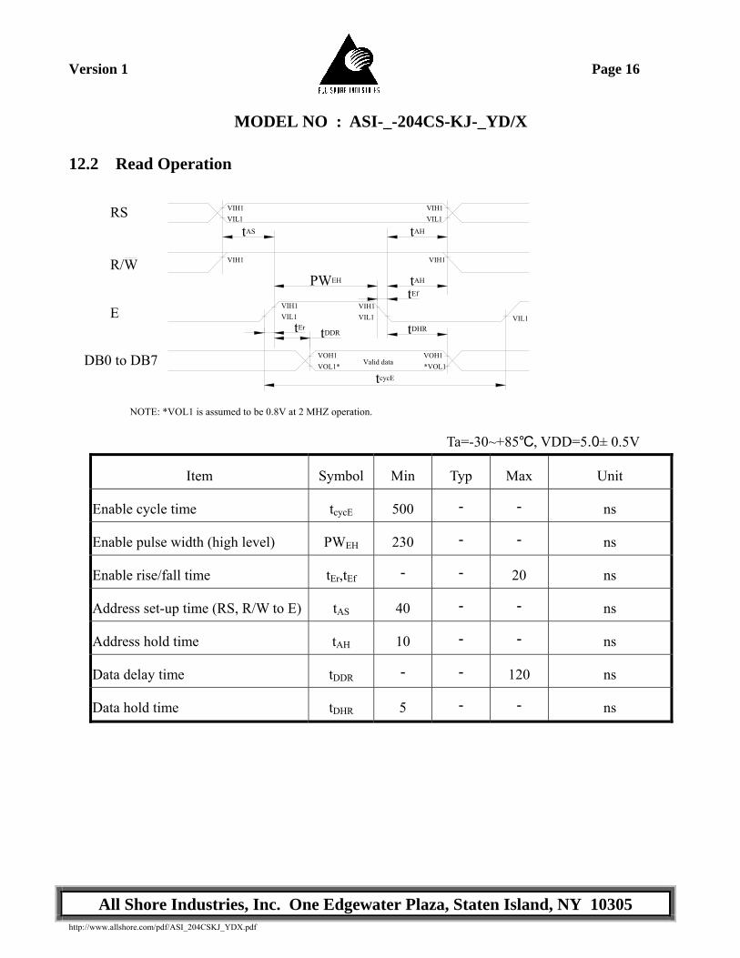
12.2 Read Operation
Ta=-30~+85℃, VDD=5.0± 0.5V
Item Symbol Min Typ Max Unit
Enable cycle time tcycE 500 - - ns
Enable pulse width (high level) PWEH 230 - - ns
Enable rise/fall time tEr,tEf - - 20 ns
Address set-up time (RS, R/W to E) tAS 40 - - ns
Address hold time tAH 10 - - ns
Data delay time tDDR - - 120 ns
Data hold time tDHR 5 - - ns
VIH1VIL1
VIH1VIL1
tcycE
VOH1VOL1*
tAS tAH
tAH
tEf
tDHR
PWEH
tErVIL1
VIH1VIL1
VIH1VIL1
RS
R/W
E
DB0 to DB7
VIH1 VIH1
VOH1*VOL1Valid data
tDDR
NOTE: *VOL1 is assumed to be 0.8V at 2 MHZ operation.
Version 1 Page 17
MODEL NO : ASI-_-204CS-KJ-_YD/X
All Shore Industries, Inc. One Edgewater Plaza, Staten Island, NY 10305 http://www.allshore.com/pdf/ASI_204CSKJ_YDX.pdf
Initializing of LCM
Power on
RS R/W DB7 DB6 DB5 DB4 DB3 DB2 DB1 DB00 0 0 0 1 1 N F * *
Wait for more than 30 ms after VDD rises to 4.5 V
Wait for more than 39us
0DB4DB7
0RS
0R/W DB6
0 0DB5
0DB1DB2DB3
1 D C BDB0
Wait for more than 39 μs
DB40
DB7R/WRS0 0
DB5DB60 0 0
DB1DB3 DB20 0 0
DB01
DB4DB7RS R/W DB6 DB5 DB1DB2DB3 DB00 0 0 0 0 0 0 1 I/D S
Initialization ends
BF can not be checked before this instruction.
Function set ( Interface is 8 bits long. )
Function set ( Display ON/OFF Control )
BF can not be checked before this instruction.
BF can not be checked before this instruction.
Function set ( Display Clear )
BF can be checked after the following instructions.When BF is not checked , the waiting time betweeninstructions is longer than execution instruction time.
8-Bit Ineterface
Wait for more than 1.53 ms
N0 1-line mode1 2-line mode 5x11 font
5x8 fontF
10
display ondisplay off
D10
Ccursor oncursor off
10
blink onblink off
1B
0
incrementdecrement mode
1I/D
0SH
entire shift on1entire shift off0
Function set ( Entry Mode Set )
Wait for more than 40 ms after VDD rises to 2.7 V
Version 1 Page 18
MODEL NO : ASI-_-204CS-KJ-_YD/X
All Shore Industries, Inc. One Edgewater Plaza, Staten Island, NY 10305 http://www.allshore.com/pdf/ASI_204CSKJ_YDX.pdf
Power on
RS R/W DB7 DB6 DB5 DB4 DB3 DB2 DB1 DB00 0 0 0 1 0 * * * *
Wait for more than 30 ms after VDD rises to 4.5 V
Wait for more than 39us
0DB4DB7
0RS
0R/W DB6
0 0DB5
0DB1DB2DB3
* * * *DB0
Wait for more than 39 μs
DB40
DB7R/WRS0 0
DB5DB60 0 0
DB1DB3 DB2* * *
DB0*
DB4DB7RS R/W DB6 DB5 DB1DB2DB3 DB00 0 0 0 0 0 * * * *
Initialization ends
BF can not be checked before this instruction.
Function set ( Interface is 8 bits long. )
Function set ( Display ON/OFF Control )
BF can not be checked before this instruction.
BF can not be checked before this instruction.
Function set ( Display Clear )
BF can be checked after the following instructions.When BF is not checked , the waiting time betweeninstructions is longer than execution instruction time.
Wait for more than 1.53ms
N0 1-line mode1 2-line mode display on
display offF
10
display ondisplay off
D10
Ccursor oncursor off
10
blink onblink off
1B
0
incrementdecrement mode
1I/D
0SH
entire shift on1entire shift off0
Function set ( Entry Mode Set )
Wait for more than 40 ms after VDD rises to 2.7 V
00 0 0 01 * ** *00 N F ** * ** *
00 1 D BC * ** *
00 0 0 10 * ** *
*00 0 1 SHI/D * * *
4-Bit Ineterface
Version 1 Page 19
MODEL NO : ASI-_-204CS-KJ-_YD/X
All Shore Industries, Inc. One Edgewater Plaza, Staten Island, NY 10305 http://www.allshore.com/pdf/ASI_204CSKJ_YDX.pdf
Quality Assurance
Screen Cosmetic Criteria Item Defect Judgment Criterion Partition
1 Spots
A)Clear Size: d mm Acceptable Qty in active area
d ≦ 0.1 Disregard
0.1<d≦ 0.2 6
0.2<d≦ 0.3 2 0.3<d 0
Note: Including pin holes and defective dots which must be within one pixel size.
B)Unclear Size: d mm Acceptable Qty in active area
d ≦ 0.2 Disregard
0.2<d≦ 0.5 6
0.5<d≦ 0.7 2 0.7<d 0
Minor
2 Bubbles in Polarize
Size: d mm Acceptable Qty in active area d≦ 0.3 Disregard
0.3<d≦ 1.0 3
1.0<d≦ 1.5 1 1.5<d 0
Minor
3 Scratch In accordance with spots cosmetic criteria. When the light
reflects on the panel surface, the scratches are not to be remarkable.
Minor
4 Allowable Density Above defects should be separated more than 30mm each other. Minor
5 Coloration
Not to be noticeable coloration in the viewing area of the LCD panels.
Back-light type should be judged with back-light on state only.
Minor
Version 1 Page 20
MODEL NO : ASI-_-204CS-KJ-_YD/X
All Shore Industries, Inc. One Edgewater Plaza, Staten Island, NY 10305 http://www.allshore.com/pdf/ASI_204CSKJ_YDX.pdf
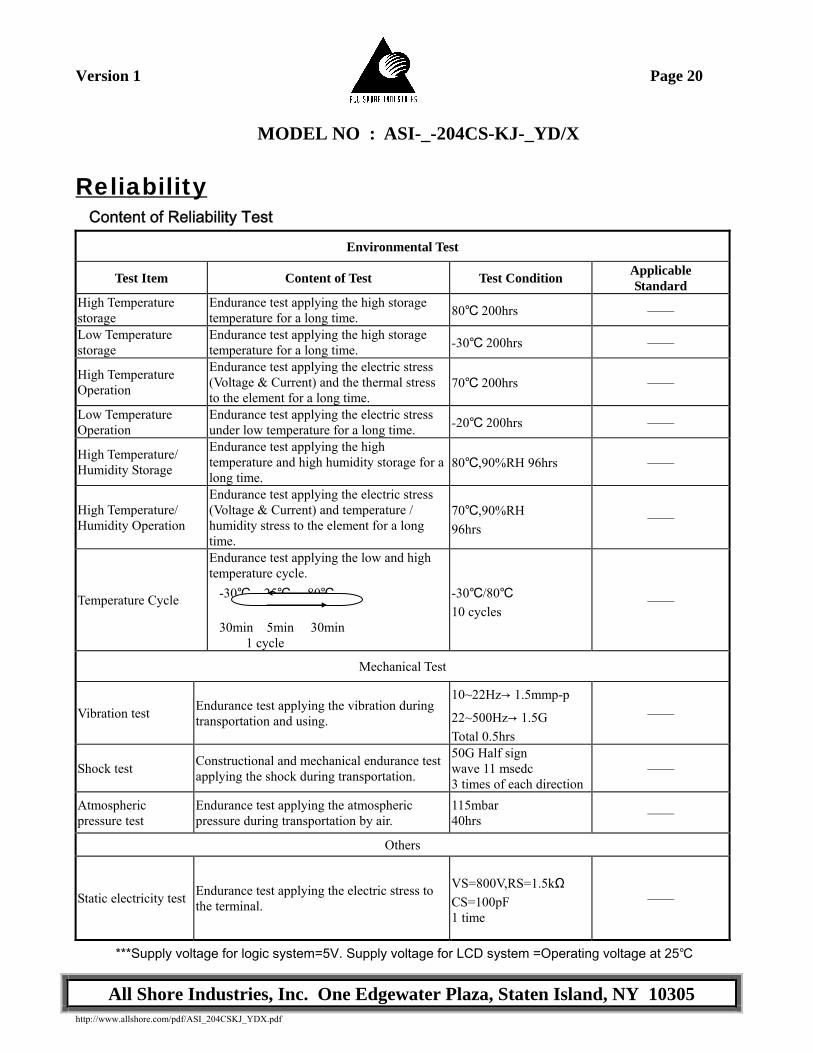
Reliability Content of Reliability Test
Environmental Test
Test Item Content of Test Test Condition Applicable Standard
High Temperature storage
Endurance test applying the high storage temperature for a long time. 80℃ 200hrs ——
Low Temperature storage
Endurance test applying the high storage temperature for a long time. -30℃ 200hrs ——
High Temperature Operation
Endurance test applying the electric stress (Voltage & Current) and the thermal stress to the element for a long time.
70℃ 200hrs ——
Low Temperature Operation
Endurance test applying the electric stress under low temperature for a long time. -20℃ 200hrs ——
High Temperature/ Humidity Storage
Endurance test applying the high temperature and high humidity storage for a long time.
80℃,90%RH 96hrs ——
High Temperature/ Humidity Operation
Endurance test applying the electric stress (Voltage & Current) and temperature / humidity stress to the element for a long time.
70℃,90%RH 96hrs
——
Temperature Cycle
Endurance test applying the low and high temperature cycle. -30℃ 25℃ 80℃ 30min 5min 30min 1 cycle
-30℃/80℃ 10 cycles
——
Mechanical Test
Vibration test Endurance test applying the vibration during transportation and using.
10~22Hz→ 1.5mmp-p
22~500Hz→ 1.5G Total 0.5hrs
——
Shock test Constructional and mechanical endurance test applying the shock during transportation.
50G Half sign wave 11 msedc 3 times of each direction
——
Atmospheric pressure test
Endurance test applying the atmospheric pressure during transportation by air.
115mbar 40hrs ——
Others
Static electricity test Endurance test applying the electric stress to the terminal.
VS=800V,RS=1.5kΩ CS=100pF 1 time
——
***Supply voltage for logic system=5V. Supply voltage for LCD system =Operating voltage at 25℃
Version 1 Page 21
MODEL NO : ASI-_-204CS-KJ-_YD/X
All Shore Industries, Inc. One Edgewater Plaza, Staten Island, NY 10305 http://www.allshore.com/pdf/ASI_204CSKJ_YDX.pdf
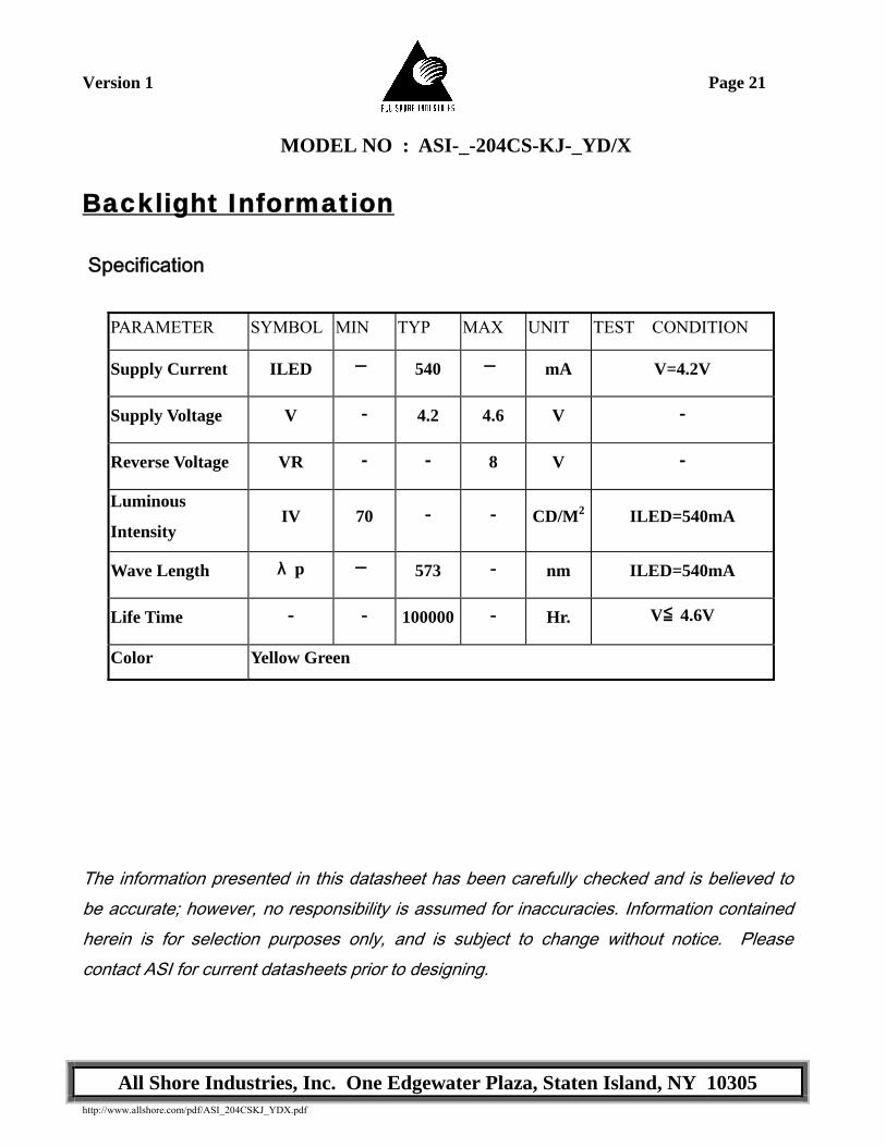
Backlight Information
Specification
PARAMETER SYMBOL MIN TYP MAX UNIT TEST CONDITION
Supply Current ILED ─ 540 ─ mA V=4.2V
Supply Voltage V - 4.2 4.6 V -
Reverse Voltage VR - - 8 V -
Luminous
Intensity IV 70 - - CD/M2 ILED=540mA
Wave Length λ p ─ 573 - nm ILED=540mA
Life Time - - 100000 - Hr. V≦ 4.6V
Color Yellow Green
The information presented in this datasheet has been carefully checked and is believed to be accurate; however, no responsibility is assumed for inaccuracies. Information contained herein is for selection purposes only, and is subject to change without notice. Please contact ASI for current datasheets prior to designing.


![axial vorgespannter Schraubverbindungen · Defekte. 5-ulik.com mittels Längensensor rspannen. Seite 14 rspannen. Seite 15 0 0 0 0 0 0 0 0 0 0 00 00 00 00 00 00 00 6 [bar] mm] rspannen](https://img.pdfslide.net/doc/110x75/5e04e535636fdb5a100c5766/axial-vorgespannter-schraubverbindungen-defekte-5-ulikcom-mittels-lngensensor.jpg)