Embed Size (px)
Citation preview

Allegro® PCB RouterTutorial
Product Version 16.0June 2007
1994–2007 Cadence Design Systems, Inc. All rights reserved.Portions © Apache Software Foundation, Sun Microsystems, Free Software Foundation, Inc., Regents ofthe University of California, Massachusetts Institute of Technology, University of Florida. Used bypermission. Printed in the United States of America.
Cadence Design Systems, Inc. (Cadence), 2655 Seely Ave., San Jose, CA 95134, USA.
Allegro PCB Router contains technology licensed from, and copyrighted by: Apache Software Foundation,1901 Munsey Drive Forest Hill, MD 21050, USA © 2000-2005, Apache Software Foundation. SunMicrosystems, 4150 Network Circle, Santa Clara, CA 95054 USA © 1994-2007, Sun Microsystems, Inc.Free Software Foundation, 59 Temple Place, Suite 330, Boston, MA 02111-1307 USA © 1989, 1991, FreeSoftware Foundation, Inc. Regents of the University of California, Sun Microsystems, Inc., ScripticsCorporation, © 2001, Regents of the University of California. Daniel Stenberg, © 1996 - 2006, DanielStenberg. UMFPACK © 2005, Timothy A. Davis, University of Florida, ([email protected]). Ken Martin, WillSchroeder, Bill Lorensen © 1993-2002, Ken Martin, Will Schroeder, Bill Lorensen. Massachusetts Instituteof Technology, 77 Massachusetts Avenue, Cambridge, Massachusetts, USA © 2003, the Board of Trusteesof Massachusetts Institute of Technology. All rights reserved.
Trademarks: Trademarks and service marks of Cadence Design Systems, Inc. contained in this documentare attributed to Cadence with the appropriate symbol. For queries regarding Cadence’s trademarks,contact the corporate legal department at the address shown above or call 800.862.4522.
Open SystemC, Open SystemC Initiative, OSCI, SystemC, and SystemC Initiative are trademarks orregistered trademarks of Open SystemC Initiative, Inc. in the United States and other countries and areused with permission.
All other trademarks are the property of their respective holders.
Restricted Permission: This publication is protected by copyright law and international treaties andcontains trade secrets and proprietary information owned by Cadence. Unauthorized reproduction ordistribution of this publication, or any portion of it, may result in civil and criminal penalties. Except asspecified in this permission statement, this publication may not be copied, reproduced, modified, published,uploaded, posted, transmitted, or distributed in any way, without prior written permission from Cadence.Unless otherwise agreed to by Cadence in writing, this statement grants Cadence customers permission toprint one (1) hard copy of this publication subject to the following conditions:
1. The publication may be used only in accordance with a written agreement between Cadence and itscustomer.
2. The publication may not be modified in any way.3. Any authorized copy of the publication or portion thereof must include all original copyright,
trademark, and other proprietary notices and this permission statement.4. The information contained in this document cannot be used in the development of like products or
software, whether for internal or external use, and shall not be used for the benefit of any other party,whether or not for consideration.
Patents: Allegro PCB Router, described in this document, is protected by U.S. Patents 5,481,695;5,510,998; 5,550,748; 5,590,049; 5,625,565; 5,715,408; 6,516,447; 6,594,799; 6,851,094; 7,017,137;7,143,341; 7,168,041.
Disclaimer: Information in this publication is subject to change without notice and does not represent acommitment on the part of Cadence. Except as may be explicitly set forth in such agreement, Cadence doesnot make, and expressly disclaims, any representations or warranties as to the completeness, accuracy orusefulness of the information contained in this document. Cadence does not warrant that use of suchinformation will not infringe any third party rights, nor does Cadence assume any liability for damages orcosts of any kind that may result from use of such information.
Restricted Rights: Use, duplication, or disclosure by the Government is subject to restrictions as set forthin FAR52.227-14 and DFAR252.227-7013 et seq. or its successor.
Allegro PCB RouterTutorial
Contents
About this Tutorial. . . . . . . . . . . . . . . . . . . . . . . . . . . . . . . . . . . . . . . . . . . . . . . . . . 7
Welcome . . . . . . . . . . . . . . . . . . . . . . . . . . . . . . . . . . . . . . . . . . . . . . . . . . . . . . . . . . . . . . 7Audience . . . . . . . . . . . . . . . . . . . . . . . . . . . . . . . . . . . . . . . . . . . . . . . . . . . . . . . . . . . . . . 7Conventions . . . . . . . . . . . . . . . . . . . . . . . . . . . . . . . . . . . . . . . . . . . . . . . . . . . . . . . . . . . . 7Special Terms . . . . . . . . . . . . . . . . . . . . . . . . . . . . . . . . . . . . . . . . . . . . . . . . . . . . . . . . . . 9Where to Find Additional Information . . . . . . . . . . . . . . . . . . . . . . . . . . . . . . . . . . . . . . . . 9How to Contact Technical Support . . . . . . . . . . . . . . . . . . . . . . . . . . . . . . . . . . . . . . . . . . . 9
Introducing PCB Router. . . . . . . . . . . . . . . . . . . . . . . . . . . . . . . . . . . . . . . . . . 11
What Your Prior Experience Should Be . . . . . . . . . . . . . . . . . . . . . . . . . . . . . . . . . . . 11What You Will Learn . . . . . . . . . . . . . . . . . . . . . . . . . . . . . . . . . . . . . . . . . . . . . . . . . . 11How to Use This Tutorial . . . . . . . . . . . . . . . . . . . . . . . . . . . . . . . . . . . . . . . . . . . . . . 12License Considerations . . . . . . . . . . . . . . . . . . . . . . . . . . . . . . . . . . . . . . . . . . . . . . . 13How PCB Router Fits in the PCB Design Process . . . . . . . . . . . . . . . . . . . . . . . . . . . 13Transferring Designs Between the Autorouter and the Layout System . . . . . . . . . . . 14Understanding the PCB Router Design File . . . . . . . . . . . . . . . . . . . . . . . . . . . . . . . . 17Understanding PCB Router’s ShapeBased™ Technology . . . . . . . . . . . . . . . . . . . . . 18
1Lesson 1: Learning Basic Concepts. . . . . . . . . . . . . . . . . . . . . . . . . . . . 21
What You Will Learn . . . . . . . . . . . . . . . . . . . . . . . . . . . . . . . . . . . . . . . . . . . . . . . . . . 21What to do Before You Begin . . . . . . . . . . . . . . . . . . . . . . . . . . . . . . . . . . . . . . . . . . . 21Starting PCB Router and Loading a Design . . . . . . . . . . . . . . . . . . . . . . . . . . . . . . . . 22
Controlling the Autorouter . . . . . . . . . . . . . . . . . . . . . . . . . . . . . . . . . . . . . . . . . . . . . . . . 26Using the Graphical User Interface (GUI) . . . . . . . . . . . . . . . . . . . . . . . . . . . . . . . . . . 27Controlling the Autorouter with the GUI . . . . . . . . . . . . . . . . . . . . . . . . . . . . . . . . . . . 29Monitoring Progress and Checking Results . . . . . . . . . . . . . . . . . . . . . . . . . . . . . . . . 33
June 2007 3 Product Version 16.0

Allegro PCB RouterTutorial
Using the Mouse to Pan and Zoom . . . . . . . . . . . . . . . . . . . . . . . . . . . . . . . . . . . . . . . . . 35Getting Information and Measuring Distance . . . . . . . . . . . . . . . . . . . . . . . . . . . . . . . . . 37Saving Your Work . . . . . . . . . . . . . . . . . . . . . . . . . . . . . . . . . . . . . . . . . . . . . . . . . . . . . . 41
Reviewing Session Command History . . . . . . . . . . . . . . . . . . . . . . . . . . . . . . . . . . . . 46What You Learned . . . . . . . . . . . . . . . . . . . . . . . . . . . . . . . . . . . . . . . . . . . . . . . . . . . 49
2Lesson 2: Placing Components. . . . . . . . . . . . . . . . . . . . . . . . . . . . . . . . . 51
What You Will Learn . . . . . . . . . . . . . . . . . . . . . . . . . . . . . . . . . . . . . . . . . . . . . . . . . . 51What to do Before You Begin . . . . . . . . . . . . . . . . . . . . . . . . . . . . . . . . . . . . . . . . . . . 51
Understanding the Basic Steps for Placing Components . . . . . . . . . . . . . . . . . . . . . . . . 52Setting Placement Rules . . . . . . . . . . . . . . . . . . . . . . . . . . . . . . . . . . . . . . . . . . . . . . 53Preplacing Connectors and Critical Components . . . . . . . . . . . . . . . . . . . . . . . . . . . . 57Placing Large Components . . . . . . . . . . . . . . . . . . . . . . . . . . . . . . . . . . . . . . . . . . . . 66Placing Small Components . . . . . . . . . . . . . . . . . . . . . . . . . . . . . . . . . . . . . . . . . . . . 78Quitting the Autorouter and Saving Placement Results . . . . . . . . . . . . . . . . . . . . . . . 83What You Learned . . . . . . . . . . . . . . . . . . . . . . . . . . . . . . . . . . . . . . . . . . . . . . . . . . . 84
3Lesson 3: Routing a PCB Design. . . . . . . . . . . . . . . . . . . . . . . . . . . . . . . 85
What You Will Learn . . . . . . . . . . . . . . . . . . . . . . . . . . . . . . . . . . . . . . . . . . . . . . . . . . 85What to do Before You Begin . . . . . . . . . . . . . . . . . . . . . . . . . . . . . . . . . . . . . . . . . . . 85Understanding How the Autorouter Works . . . . . . . . . . . . . . . . . . . . . . . . . . . . . . . . . 86Setting Routing Rules . . . . . . . . . . . . . . . . . . . . . . . . . . . . . . . . . . . . . . . . . . . . . . . . 100Autorouting With a Do File . . . . . . . . . . . . . . . . . . . . . . . . . . . . . . . . . . . . . . . . . . . . 104Monitoring Autorouting Progress . . . . . . . . . . . . . . . . . . . . . . . . . . . . . . . . . . . . . . . 111What You Learned . . . . . . . . . . . . . . . . . . . . . . . . . . . . . . . . . . . . . . . . . . . . . . . . . . 116
4Lesson 4: Setting Rules and Constraints . . . . . . . . . . . . . . . . . . . . . 117
What You Will Learn . . . . . . . . . . . . . . . . . . . . . . . . . . . . . . . . . . . . . . . . . . . . . . . . . 117What to do Before You Begin . . . . . . . . . . . . . . . . . . . . . . . . . . . . . . . . . . . . . . . . . . 117Understanding the Autorouter’s Hierarchical Rules . . . . . . . . . . . . . . . . . . . . . . . . . 118Using Commands to Set Rules and Control the Autorouter . . . . . . . . . . . . . . . . . . . 121
June 2007 4 Product Version 16.0

Allegro PCB RouterTutorial
Selecting Connections and Autorouting . . . . . . . . . . . . . . . . . . . . . . . . . . . . . . . . . . 125Using Routing Keepin Regions . . . . . . . . . . . . . . . . . . . . . . . . . . . . . . . . . . . . . . . . . 128Controlling Whether Nets are Routed With Starburst or Daisy-Chain Wiring . . . . . . 130Routing Nets . . . . . . . . . . . . . . . . . . . . . . . . . . . . . . . . . . . . . . . . . . . . . . . . . . . . . . . 133What You Learned . . . . . . . . . . . . . . . . . . . . . . . . . . . . . . . . . . . . . . . . . . . . . . . . . . 137
5Lesson 5: Interactive Routing and Editing . . . . . . . . . . . . . . . . . . . . 139
What You Will Learn . . . . . . . . . . . . . . . . . . . . . . . . . . . . . . . . . . . . . . . . . . . . . . . . . 139What to do Before You Begin . . . . . . . . . . . . . . . . . . . . . . . . . . . . . . . . . . . . . . . . . . 139Interactively Routing . . . . . . . . . . . . . . . . . . . . . . . . . . . . . . . . . . . . . . . . . . . . . . . . . 140Editing Wires and Vias . . . . . . . . . . . . . . . . . . . . . . . . . . . . . . . . . . . . . . . . . . . . . . . 159What You Learned . . . . . . . . . . . . . . . . . . . . . . . . . . . . . . . . . . . . . . . . . . . . . . . . . . 170Congratulations! . . . . . . . . . . . . . . . . . . . . . . . . . . . . . . . . . . . . . . . . . . . . . . . . . . . . 170
Index. . . . . . . . . . . . . . . . . . . . . . . . . . . . . . . . . . . . . . . . . . . . . . . . . . . . . . . . . . . . . . . 171
June 2007 5 Product Version 16.0

Allegro PCB RouterTutorial
June 2007 6 Product Version 16.0

Allegro PCB RouterTutorial
About this Tutorial
Welcome
Allegro® PCB Router is a printed circuit board (PCB) design automation tool that runs onUNIX and Windows platforms. You can use PCB Router to automatically or interactively placeand route dense surface-mount (SMD) and through-pin (PTH) designs.
All versions of PCB Router (200 and 600 series) include a graphical user interface (GUI) andthe same adaptive, ShapeBased technology. SMD pads, through-pins, wires, and othercircuit elements are modeled as basic geometric shapes. Each shape can have rulesassociated with it which enforce design constraints such as component spacing andorientation, wire width and clearance, timing, noise, and crosstalk.
This tutorial consists of a book and several accompanying files. The tutorial files are copiedto a tutorial directory when you install the tool on your computer or network.Separate instructions are provided for Windows and UNIX platforms when steps orprocedures differ between these platforms. The majority of the screen shots in this tutorial arefrom the Windows environment unless otherwise noted. For further details on using thistutorial, see Introducing PCB Router on page 11.
Audience
This tutorial is written for novice users who are familiar with current methods and practicesused to design printed circuit boards.
Conventions
The following fonts, characters, and styles are used to identify or represent different types ofinformation.
■ Boldface courier type identifies text that you type exactly as shown, such ascommands, keywords, and other syntax elements.
For example:
Type rule pcb (width .008) in the command entry box.
June 2007 7 Product Version 16.0

Allegro PCB RouterTutorialAbout this Tutorial
Syntax examples and command examples that are not entered by you from the keyboardare not bold. For example:
(boundary (rect pcb 0 0 9000 4000))
■ Italic type identifies titles of books and emphasizes portions of text.
For example:
See the Allegro PCB Router User Guide for information about starting PCB Router.
Italicized words enclosed in angle brackets (<>) are placeholders for keywords, values,filenames, or other information that you must supply. For example:
<directory_path_name>
■ Courier type identifies prompts, messages, and other output text that appears on yourscreen. For example, if you misspell the command define as defin, an error messagedisplays in the output window.
‘Syntax error in command: token 1 = defin’
Courier type also identifies operating system commands and switches.
Courier type enclosed in brackets ([ ]) identifies keys on your keyboard and mousebuttons.
For example, [Shift] means the shift key. The carriage return key is labeled Enter onsome keyboards and Return on others. This manual uses [Enter].
■ Mouse buttons are identified by two uppercase letters enclosed in brackets.
[LB] left button
[MB] middle button
[RB] right button
If you have a 2-button mouse, press [Alt] and [RB] simultaneously when you see[MB].
■ If a task requires a series of steps that are different on different computer platforms,separate procedures are provided.
For example:
Start the tool by using the Startup dialog box (Windows)
➤ Click Start on the task bar, slide the pointer to Programs, and choose PCB Router.
Start the tool by using the Startup dialog box (UNIX)
June 2007 8 Product Version 16.0
Allegro PCB RouterTutorialAbout this Tutorial
➤ Change your current directory to the PCB Router tutorial directory.
Special Terms
The following special terms are used in this manual.
■ The word enter used with commands means type the command and press [Enter].For example:
“Enter the command grid wire 1” means:
1. Type grid wire 1.
2. Press [Enter].
■ Click means press and release the left mouse button.
■ Click-middle means press and release the middle mouse button.
■ Click-right means press and release the right mouse button.
■ Drag means press and hold the left mouse button while you move the pointer.
■ Drag [MB]means press and hold the middle mouse button while you move the pointer.
■ Double-click means press and release the left mouse button twice in rapid succession.
■ Click twice means click two times at the same location in the work area.
■ Switch refers to one or more characters preceded by a dash (-). You can use a switchwhen you start PCB Router.
Where to Find Additional Information
To access additional technical documentation from within the PCB Router user interface,display the online Help page by choosing Help – Documentation from the main menu.
How to Contact Technical Support
If you have questions about installing or using PCB Router, you can visit the CadenceSupport web site at:
http://sourcelink.cadence.com /supportcontacts.htm
June 2007 9 Product Version 16.0

Allegro PCB RouterTutorialAbout this Tutorial
June 2007 10 Product Version 16.0

Allegro PCB RouterTutorial
Introducing PCB Router
This tutorial teaches you how to use PCB Router to place and route printed circuit board(PCB) designs.
What Your Prior Experience Should Be
The tutorial is written for printed circuit board designers who understand current designmethods and practices but have little or no experience using PCB Router.
You are expected to know how to:
■ start an application.
■ use a mouse.
■ open and close windows on a Windows or UNIX platform.
What You Will Learn
Each lesson in this tutorial covers a set of topics that are important to understanding the basicuse and operation of the routing and placement tools. The tutorial includes this introductorychapter and five lessons that cover the following areas.
■ Basic Concepts
■ Placing Components
■ Autorouting
■ Setting Rules and Controlling the Autorouter
■ Interactively Routing and Editing
June 2007 11 Product Version 16.0

Allegro PCB RouterTutorialIntroducing PCB Router
How to Use This Tutorial
This tutorial is designed as a step-by-step process for learning how to use PCB Router. Theinformation you learn in a lesson builds upon the previous lessons. However, it is possible touse each lesson as a separate tutorial.
Note: If you are only interested in learning about interactive routing, you can skip the firstthree lessons. However, you will need to complete Lesson 4. This lesson includes informationon setting rules, which is relevant to interactive routing and editing.
This book is accompanied by a series of lesson files. You use the book with these files andthe PCB Router software to learn by doing.
Where to find the Accompanying Lesson Files
The Tutorial Lesson files are delivered with your PCB Router software on the installation CD.Once PCB Router is installed, you can access these files from the following directory on thecomputer where your PCB Router software resides:
On Windows platforms:
<install_directory>\share\specctra\tutorial
On Unix platforms:
<install_directory>/share/specctra/tutorial
This lesson . . . teaches you to . . .
Lesson 1, Learning the Basics use the autorouter’s graphical user interface(GUI).
Lesson 2, Placing Components place components automatically andinteractively.
Lesson 3, Autorouting a PCB Design automatically route a PCB design.
Lesson 4, Setting Rules and Controlling theAutorouter
set rules and routing options to control theautorouter.
Lesson 5, Interactive Routing and Editing route interactively and edit the routing.
June 2007 12 Product Version 16.0

Allegro PCB RouterTutorialIntroducing PCB Router
License Considerations
Your PCB Router license must have the PlaceBase feature to complete the work in Lesson 2and the EditRoute feature to complete the work in Lesson 5.
Important
Depending on your specific license and the product you choose when you start PCBRouter, you may occasionally encounter a licensing error when working throughprocedures in some lessons. The Licensing Error dialog box and a sample errormessage is shown in the following figure.
Figure 1-1 Licensing Error Dialog Box
Note: These errors will not prevent you from completing a lesson. Simply click theIgnore Feature for This Session button to proceed.
Tip
License error messages warn you of unavailable software features in your license.To avoid these messages, select the Allegro PCB Router XL product (if you arelicensed to do so) when starting PCB Router to complete a tutorial lesson.Otherwise, choose the product with the “richest feature set” from the product list thatis presented to you at startup.
For further details on PCB Router Licensing, see Chapter 1 of the Allegro PCB Router UserGuide.
How PCB Router Fits in the PCB Design Process
PCB Router extends your PCB CAD system by adding automatic and interactive placementand routing tools. You use PCB Router to place components and route your printed circuitboard design.
June 2007 13 Product Version 16.0
Allegro PCB RouterTutorialIntroducing PCB Router
After you create a PCB database in Allegro PCB Editor (or another supported layout editor),you translate the design data to a PCB Router Design file. You place and route the design inPCB Router, save the results, and then merge the placement and routing data with youroriginal PCB database.
The Autorouter in the PCB Design Process
Transferring Designs Between the Autorouter and the Layout System
Each PCB layout system stores design information in a unique format. However, the filesused by PCB Router to store design data are the same regardless of the layout system youuse.
You transfer your printed circuit board design between PCB Router and the layout system bytranslating the design data from one format to the other. All files that are read and written byPCB Router are plain text files. They are described in the following table.
PCB Router Design Data Files
File Type Naming Convention Description
Design <filename>.dsn Created by translating design informationfrom the layout system. Contains PCBboundary data, layer definitions, padstackdefinitions, component data, netlist,preroutes, and design rules.
PCB Editor PCB Router
June 2007 14 Product Version 16.0

Allegro PCB RouterTutorialIntroducing PCB Router
Some layout systems require intermediate text files to transfer a PCB design to and from PCBRouter. Other systems read and write PCB Router’s files directly without intermediate files.The files that are needed to transfer designs between PCB Router and several popular layoutsystems are described in the following table.
Session <filename>.ses Created by the autorouter. Contains a pointerto the original design file, placement and routedata, gate, subgate, pin, and terminatorinformation.
Routes <filename>.rte Created by the autorouter. Contains routedata that can be translated to your layoutsystem and read by the autorouter.
Wires <filename>.w Created by the autorouter. Contains routedata that can be read by the autorouter only.
Intermediate Design Files
This layout system . . . uses . . . that contains . . .
PCB Editor <board_name>.brd all PCB design data, includingnets, properties, components,padstacks, preroutes, PCBboundary, and rules.
Board Station tech.tech layer definitions and rules.
geoms_ascii image definitions, PCB outline,keepout and keepin areas, andrules.
nets.nets a netlist.
traces.traces
(Optional)
preroutes, area fill information,and high speed topologyspecifications.
gates.gates
(Optional)
gate and pin swap information.
PCB Router Design Data Files, continued
File Type Naming Convention Description
June 2007 15 Product Version 16.0
Allegro PCB RouterTutorialIntroducing PCB Router
Many PCB layout systems have built-in features to transfer designs to and from PCB Router.Some layout systems include a choice on a menu or a separate GUI to simplify the transferprocess. Refer to the documentation for your layout system or the documentation that wasincluded with your PCB Router translator to determine how to transfer designs between yourlayout system and PCB Router.
pins.pins
(Optional)
Properties attached to pins
testpoints.testpoints
(Optional)
Testpoint information
mfg/neutral_file
(Optional)
Pin X,Y coordinates
PADS ASCII output All PCB design data, includingnets, components, padstacks,preroutes, PCB boundary, andrules
PCAD PDIF All PCB design data, includingnets, components, padstacks,preroutes, PCB boundary, andrules
Protel Protel text file Writes the autorouting design fileand reads routes and sessionfiles directly
Intermediate Design Files, continued
This layout system . . . uses . . . that contains . . .
June 2007 16 Product Version 16.0

Allegro PCB RouterTutorialIntroducing PCB Router
Understanding the PCB Router Design File
The PCB Router Design file is a text file that contains the information needed to represent aprinted circuit board in PCB Router. The PCB outline, layers, components, padstacks, nets,and preroutes are represented in the Design file in five sections. These five sections aredescribed in the following table.
Because the PCB Router Design file is a text file, you can view it in PCB Router using a reportwindow by choosing Report – Design. You can also view it using most any text editor.
Note: Do not edit the Design file in a text editor. Most translators use the Design file to mergethe routing data with the original layout system database. If you change the Design file andit’s no longer synchronized with the layout system database, the translation of route data toyour layout system could fail. If you need to make a change to the design data, make thechange in your layout system and translate the revised design to the PCB Router Design file.
Using a text editor, you can search for keywords. In UNIX, you can use vi, emacs, or textedit.In Windows, you can use Notepad or Write. If the Design file is too large for Notepad, useWrite with the no conversion option.
In Windows, you cannot view a Design file in a text editor while the file is loaded in PCBRouter. However, you can copy and rename the Design file to accomplish this.
This design file section . . . Contains this information . . .
Structure Working units, layer definitions, PCB boundary, powerplanes, region rules, PCB keepouts, via ids, globalrules, grid definitions.
Placement Component instances that consist of image names,reference designators, X,Y locations, PCB side, androtation.
Library Image definitions that include pin names and pinlocations, pin definitions, and padstack definitions.
Network Net list (net names and pin lists), class definitions, classto class definitions, group definitions, differential pairdefinitions, and net, class, or group rules.
Wiring Preroute information.
June 2007 17 Product Version 16.0

Allegro PCB RouterTutorialIntroducing PCB Router
Understanding PCB Router’s ShapeBased™ Technology
PCB Router succeeds in routing large, dense designs because of its ShapeBasedtechnology. The PCB Router autorouter differs from traditional grid-mapped systemsbecause it models pins, pads, wires, and vias as true shapes. Grid-mapped systems definethese shapes as grid points. Each pin, pad, wire, and via is defined in terms of the grid pointsit occupies.
The following figure shows the basic difference between the ShapeBased system and a grid-mapped approach.
Figure 1-2 ShapeBased vs. Grid-mapped Object Modelling
While grid-mapped modeling wastes space, its greater weaknesses are its excessivememory and storage requirements. PCB Router’s ShapeBased approach only requiresmemory for storing shapes, not grid points. The following figure illustrates the differencebetween ShapeBased and grid-mapped memory requirements.
June 2007 18 Product Version 16.0

Allegro PCB RouterTutorialIntroducing PCB Router
ShapeBased vs. Grid-Mapped Memory Requirements
Another advantage of PCB Router’s ShapeBased technology is its support of complex designrules. Each shape on each layer inherits its own unique set of design rules. This means youcan comply with the most complicated design requirements without resorting to tricks andwork-arounds during placement and routing.
June 2007 19 Product Version 16.0

Allegro PCB RouterTutorialIntroducing PCB Router
June 2007 20 Product Version 16.0

Allegro PCB RouterTutorial
1Lesson 1: Learning Basic Concepts
What You Will Learn
This lesson explains the autorouter user interface and how to perform basic design tasks.
In this lesson, you will learn how to:
■ start the autorouter and load a design.
■ use the graphical user interface (GUI) for commands.
■ pan and zoom within the Design window.
■ measure distance and get information about design objects.
■ save your work.
■ review a session's command history.
This lesson takes about 45 minutes to complete.
What to do Before You Begin
Before you begin this lesson, do the following.
■ Read About this Tutorial on page 7 which explains the conventions, terminology, andsymbols that are used throughout this tutorial.
■ Read What You Will Learn on page 11 to determine the lessons that should becompleted to satisfy your specific learning requirements.
■ Make sure you can access the Tutorial Lesson files. For information on the location ofthese files, see Where to find the Accompanying Lesson Files on page 12.
■ Read License Considerations on page 13 which notes important license information tokeep in mind while working through the lessons in the tutorial.
■ Make sure that PCB Router has been installed properly on your computer or network.
June 2007 21 Product Version 16.0

Allegro PCB RouterTutorialLesson 1: Learning Basic Concepts
Starting PCB Router and Loading a Design
When you start the autorouter, you must load a Design (.dsn) file. The Design file is a textfile that contains all the PCB design information that is needed by the autorouter.
Note: You can also start the autorouter using a Session (.ses) file, which links the routingand placement data to a Design file. You will learn more about Session files later.
In this lesson, you use the PCB Router Startup dialog box to start the autorouter and load aDesign file. The procedure varies depending on whether you are using a Windows or UNIXplatform. Follow the procedure for your specific platform. You will use these same basic stepsfrequently throughout this tutorial. If a procedure is not specifically labeled Windows or UNIX,then it is written for both.
Task: Start PCB Router using the Startup dialog box (Windows)
Procedure
1. Choose Start – Programs – Allegro SPB <version> – PCB Router
The Startup dialog box appears.
You need to specify a Design file to start the autorouter. You can type the name of theDesign file in the Design/Session File data entry box or you can use the Browse buttonto search for one.
2. Click the Browse button to the right of the Design/Session File data entry box.
The Open dialog box appears.
June 2007 22 Product Version 16.0
Allegro PCB RouterTutorialLesson 1: Learning Basic Concepts
3. Navigate to the Allegro PCB Router Tutorial directory. See Where to find theAccompanying Lesson Files on page 12 for the location of this directory.
4. Open lesson1.dsn from the Files list.
The path and filename appear in the Design/Session File data entry box.
5. Click Start Allegro PCB Router.
The Product Selection dialog box appears.
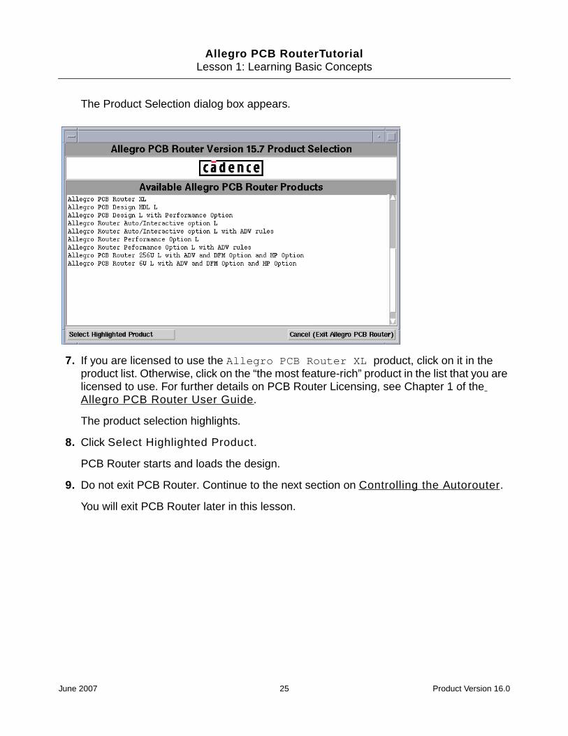
6. If you are licensed to use the Allegro PCB Router XL product, click on it in theproduct list. Otherwise, click on the the most “feature-rich” product in the list that you arelicensed to use. For further details on PCB Router licensing, products and features, referto Chapter 1 of the Allegro PCB Router User Guide.
The product selection highlights.
7. Click Select Highlighted Product.
PCB Router starts and loads the design.
8. Do not exit PCB Router. Proceed to the next section on Controlling the Autorouter.
You will exit PCB Router later in this lesson.
June 2007 23 Product Version 16.0

Allegro PCB RouterTutorialLesson 1: Learning Basic Concepts
Task: Start the Autorouter using the Startup dialog box (UNIX)
Procedure
1. Change to the Allegro PCB Router Tutorial directory. See Where to find theAccompanying Lesson Files on page 12 for the location of this directory.
2. Enter specctra at the shell prompt.
The Startup dialog box opens.
You need to specify a Design file to start the autorouter. You can type the name of theDesign file in the Design/Session File data entry box or you can use the Browse buttonto search for a file.
3. Click the Browse button to the right of the Design/Session File data entry box.
4. The Select File dialog box opens.
5. Select lesson1.dsn from the files directory and click OK.
6. Click Start Allegro PCB Router.
June 2007 24 Product Version 16.0
Allegro PCB RouterTutorialLesson 1: Learning Basic Concepts
The Product Selection dialog box appears.
7. If you are licensed to use the Allegro PCB Router XL product, click on it in theproduct list. Otherwise, click on the “the most feature-rich” product in the list that you arelicensed to use. For further details on PCB Router Licensing, see Chapter 1 of theAllegro PCB Router User Guide.
The product selection highlights.
8. Click Select Highlighted Product.
PCB Router starts and loads the design.
9. Do not exit PCB Router. Continue to the next section on Controlling the Autorouter.
You will exit PCB Router later in this lesson.
June 2007 25 Product Version 16.0
Allegro PCB RouterTutorialLesson 1: Learning Basic Concepts
Controlling the Autorouter
In the following sections, you will learn how to use the GUI to control the autorouter, how toautoroute a design, monitor progress, and examine the results.
You control the autorouter by:
■ entering console commands.
■ running a command file (Do file).
■ using the GUI to enter commands.
In a later lesson, you will enter console commands and use a Do file to control the autorouter.In this lesson you focus on the use of the GUI.
June 2007 26 Product Version 16.0
Allegro PCB RouterTutorialLesson 1: Learning Basic Concepts
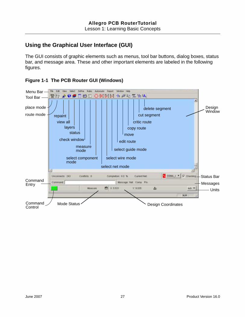
Using the Graphical User Interface (GUI)
The GUI consists of graphic elements such as menus, tool bar buttons, dialog boxes, statusbar, and message area. These and other important elements are labeled in the followingfigures.
Figure 1-1 The PCB Router GUI (Windows)
Menu Bar
place mode
route mode
Status Bar
Messages
Tool Bar
CommandEntry
Command
Units
repaint
view alllayers
status
measuremode
select net mode
select wire mode
check window
select componentmode
select guide mode
edit route
move
copy route
critic route
cut segment
delete segment DesignWindow
Mode Status Design CoordinatesControl
June 2007 27 Product Version 16.0
Allegro PCB RouterTutorialLesson 1: Learning Basic Concepts
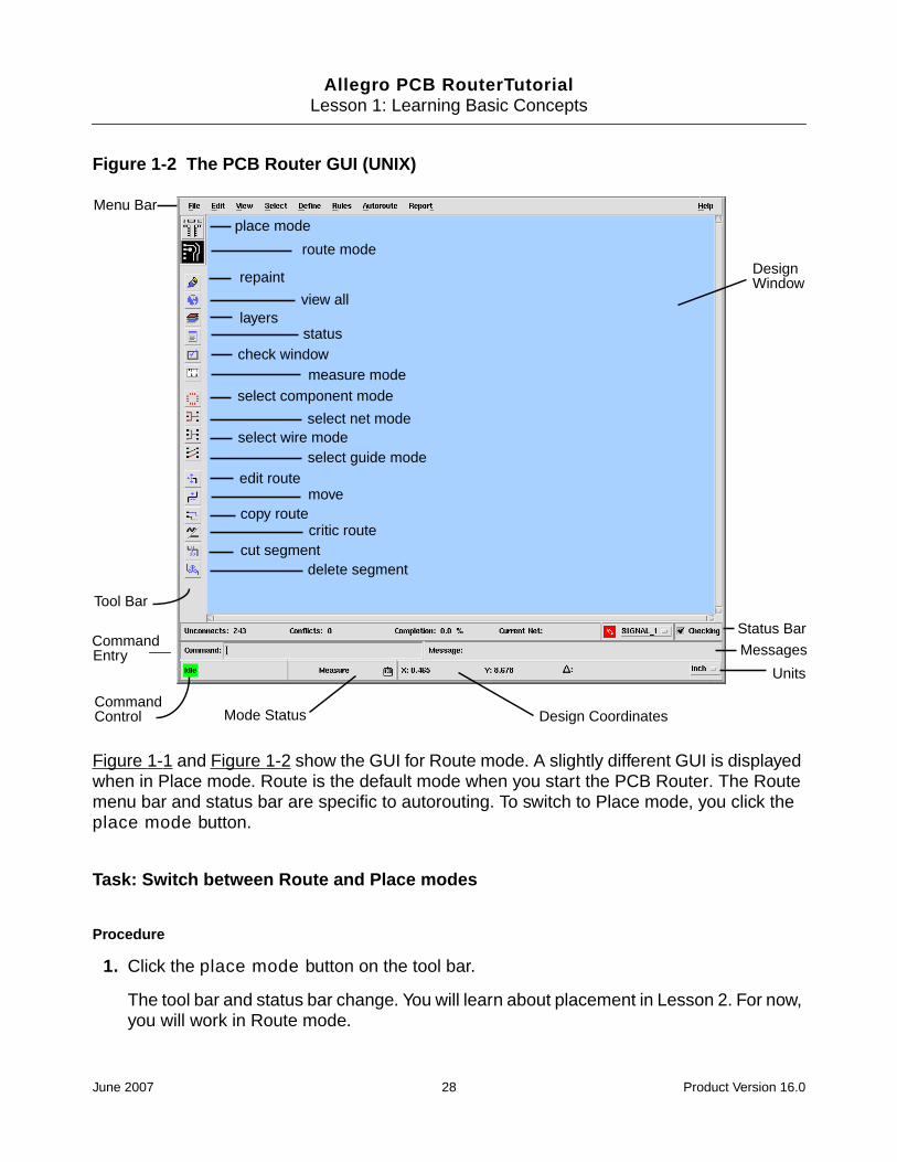
Figure 1-2 The PCB Router GUI (UNIX)
Figure 1-1 and Figure 1-2 show the GUI for Route mode. A slightly different GUI is displayedwhen in Place mode. Route is the default mode when you start the PCB Router. The Routemenu bar and status bar are specific to autorouting. To switch to Place mode, you click theplace mode button.
Task: Switch between Route and Place modes
Procedure
1. Click the place mode button on the tool bar.
The tool bar and status bar change. You will learn about placement in Lesson 2. For now,you will work in Route mode.
place mode
route mode
Menu Bar
Tool Bar
CommandEntry
DesignWindow
Status Bar
Messages
Units
CommandMode Status Design CoordinatesControl
repaint
view alllayers
status
measure modecheck window
select component mode
select net modeselect wire mode
select guide modeedit route
movecopy route
critic routecut segment
delete segment
June 2007 28 Product Version 16.0

Allegro PCB RouterTutorialLesson 1: Learning Basic Concepts
2. Click the route mode button on the tool bar.
Controlling the Autorouter with the GUI
The easiest way to control the autorouter is to use the GUI. If you use the GUI, you do notneed to know command syntax. You only need to know the task you want to complete.
In the following procedure, you use the GUI to autoroute the printed circuit board shown inthe following figure. You will see how easy it is to automatically route a design using the GUI.
Figure 1-3 lesson1.dsn (unrouted)
Task: Use the GUI to autoroute a printed circuit board
Procedure
1. Click Autoroute – Route.
June 2007 29 Product Version 16.0

Allegro PCB RouterTutorialLesson 1: Learning Basic Concepts
The AutoRoute dialog box opens.
2. Select the Basic option at the top of the dialog box.Note that 25 route passes are used by default.
3. Click OK.
The autorouter begins routing the design.
While the design is routing, note that a red Pause button appears in the control area.You can use this button to pause or stop the autorouter. When the autorouter finishes,the Pause button in the control area is replaced by a green Idle button.
Wait for the autorouter to complete.
Note: If you encounter a Licensing Error dialog box, click the Ignore Feature for ThisSession button to continue on. See License Considerations on page 13 for furtherdetails.
Once fully routed, your design should look like the following figure.
June 2007 30 Product Version 16.0

Allegro PCB RouterTutorialLesson 1: Learning Basic Concepts
Figure 1-4 lesson1.dsn (fully routed)
4. View the transcript of session information in the Output window. On UNIX platforms, theOutput window is the shell in which you started the autorouter.
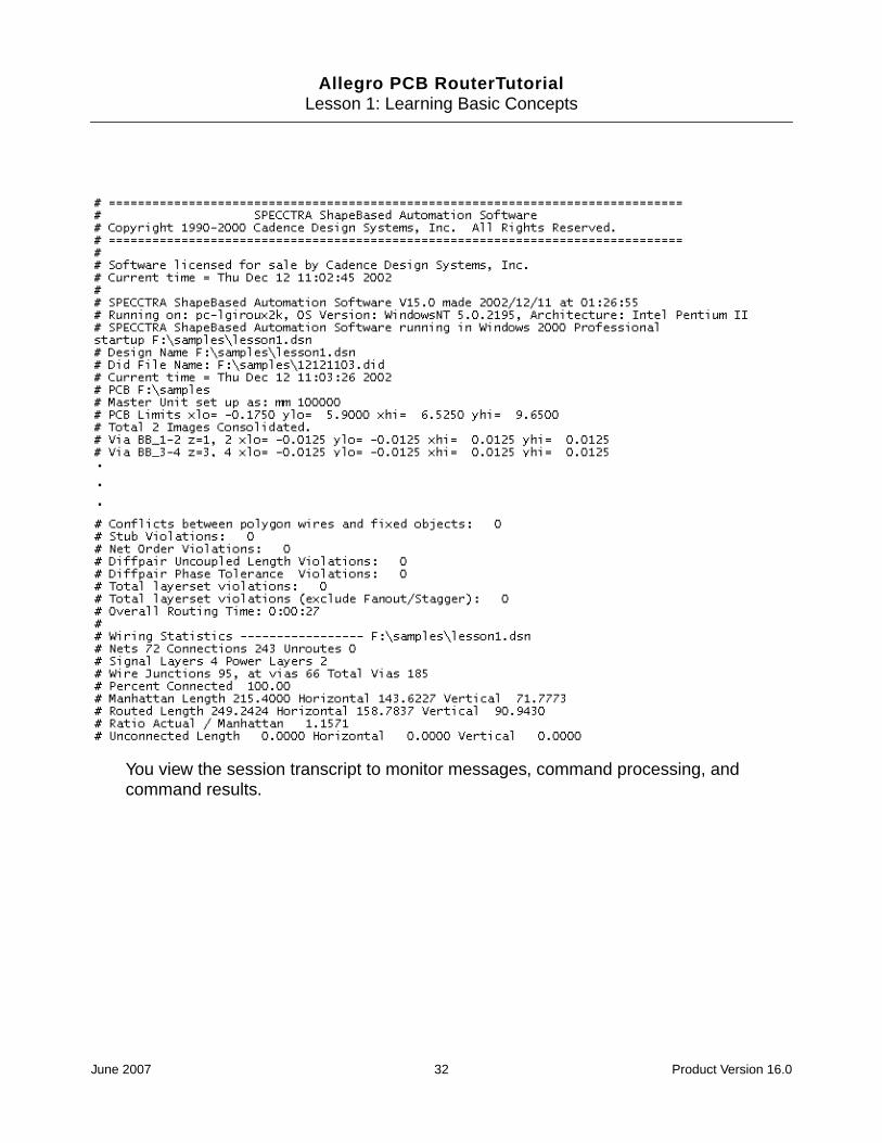
Use the Output window scroll bars to browse the information.
The Information in the Output window includes the version number and routing results.When warnings or error messages are generated, they also appear in the Outputwindow. A portion of a typical session transcript follows.
June 2007 31 Product Version 16.0
Allegro PCB RouterTutorialLesson 1: Learning Basic Concepts
You view the session transcript to monitor messages, command processing, andcommand results.
.
.
.
June 2007 32 Product Version 16.0

Allegro PCB RouterTutorialLesson 1: Learning Basic Concepts
Monitoring Progress and Checking Results
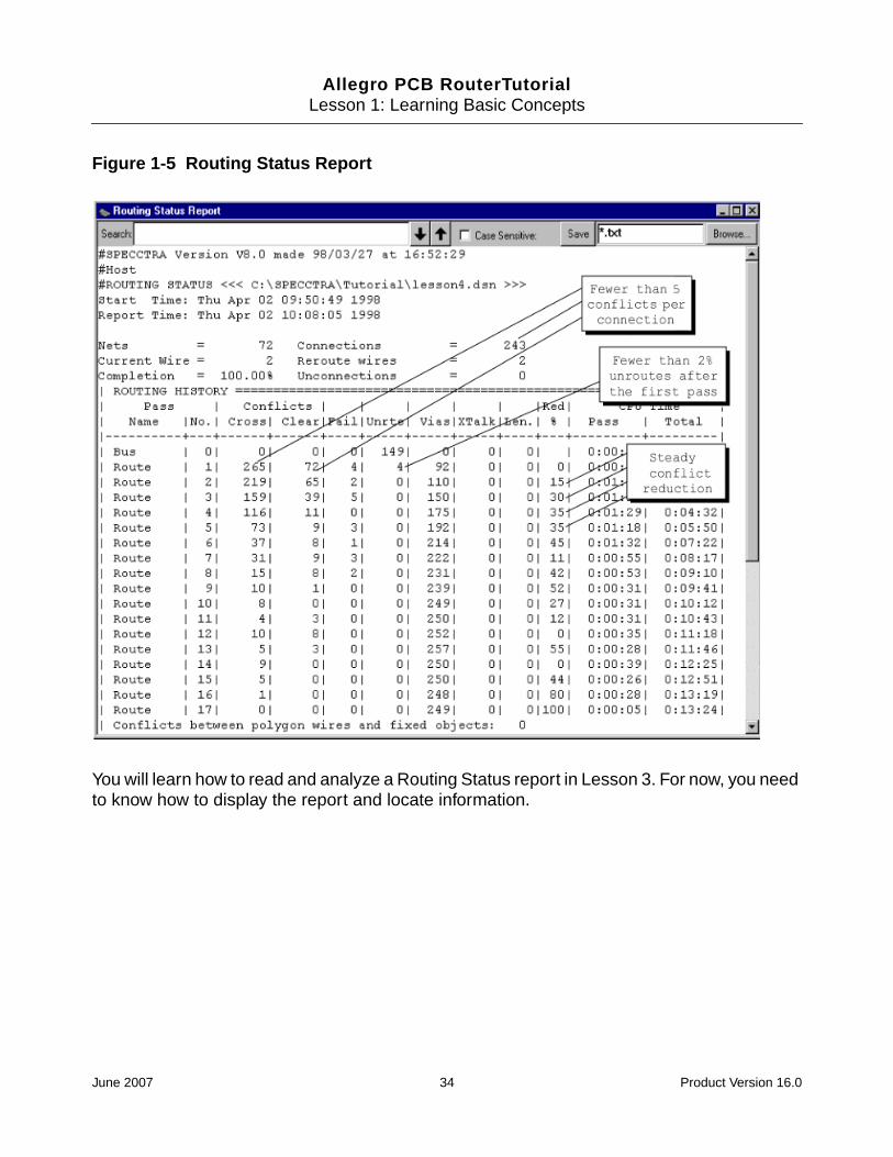
PCB Router generates a transcript of your work session in the Output window unless youredirect it to a file. In addition, a status file logs each routing command and the results of eachpass. The status file is useful for documenting session progress and monitoring routingresults. In the following procedure, you display a Routing Status Report and locateinformation by searching.
Task: Locate information in the routing status report
Procedure
1. Click the Status Report button on the tool bar. See Figure 1-1 on page 27 forassistance.
The Routing Status Report window opens.
You will search for the total number of connections in the design.
2. Enter connections in the Search entry box and click on the down arrow symbol.
Connections is highlighted.
The number to the right is the total number of connections in the design.
3. Use the scroll bars to observe the summary at the end of the report. The summary reportincludes the total number of vias used, total wire length, ratio of the manhattan length tothe routed length, and the distribution of routing per signal layer.
4. Close the report.
On the Windows platform, click the x button in the top-right corner of the report window.
On a UNIX platform, click Close at the bottom of the report window.
The following figure shows the Routing Status Report.
June 2007 33 Product Version 16.0
Allegro PCB RouterTutorialLesson 1: Learning Basic Concepts
Figure 1-5 Routing Status Report
You will learn how to read and analyze a Routing Status report in Lesson 3. For now, you needto know how to display the report and locate information.
June 2007 34 Product Version 16.0

Allegro PCB RouterTutorialLesson 1: Learning Basic Concepts
Using the Mouse to Pan and Zoom
You zoom in and magnify an area of the design by using the middle mouse button to drag thepointer diagonally from the lower left to the upper right corner of the area you want to magnify.As you drag the pointer, PCB Router dynamically changes your view.
You zoom out by dragging the pointer diagonally from upper right to lower left.
If you drag the pointer horizontally, the autorouter fits the whole design in the view.
You pan by clicking the middle mouse button on the point that you want to be the center ofyour view.
If you have a three button mouse, you use the middle mouse button to zoom and pan yourview of the design. If you have a two button mouse, you hold down the [Alt] or [◆ ] key and usethe right mouse button to zoom and pan.
Task: Zoom and pan using a three button mouse
Procedure
1. Identify an area of the design where you want to zoom in.
2. Using the middle mouse button, drag the pointer from lower left to upper right to enclosethe area and release the mouse button to zoom in.
3. Repeat the previous step to zoom in again.
4. Move the pointer left, right, above, or below the center of the current view.
5. Click the middle mouse button.
The location of the pointer becomes the new center of view.
6. Repeat the previous step several times.
Each time you click, the location of the pointer becomes the new center of view.
7. Drag the pointer diagonally from upper right to lower left to zoom out.
8. Click the View All button on the tool bar to fit the entire design in the view.
To zoom and pan using a two button mouse, you hold down the [Alt] or [ ◆ ] key and use theright mouse button.
June 2007 35 Product Version 16.0
Allegro PCB RouterTutorialLesson 1: Learning Basic Concepts
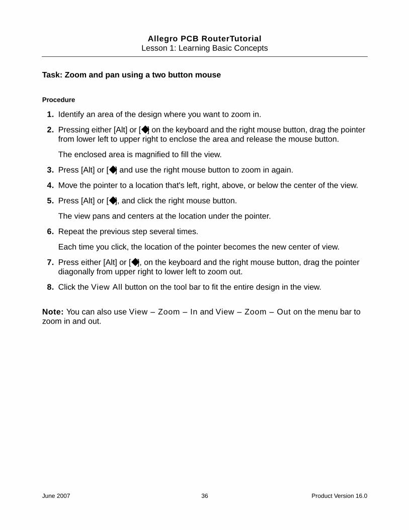
Task: Zoom and pan using a two button mouse
Procedure
1. Identify an area of the design where you want to zoom in.
2. Pressing either [Alt] or [◆ ] on the keyboard and the right mouse button, drag the pointerfrom lower left to upper right to enclose the area and release the mouse button.
The enclosed area is magnified to fill the view.
3. Press [Alt] or [◆ ] and use the right mouse button to zoom in again.
4. Move the pointer to a location that's left, right, above, or below the center of the view.
5. Press [Alt] or [◆ ], and click the right mouse button.
The view pans and centers at the location under the pointer.
6. Repeat the previous step several times.
Each time you click, the location of the pointer becomes the new center of view.
7. Press either [Alt] or [◆ ], on the keyboard and the right mouse button, drag the pointerdiagonally from upper right to lower left to zoom out.
8. Click the View All button on the tool bar to fit the entire design in the view.
Note: You can also use View – Zoom – In and View – Zoom – Out on the menu bar tozoom in and out.
June 2007 36 Product Version 16.0

Allegro PCB RouterTutorialLesson 1: Learning Basic Concepts
Getting Information and Measuring Distance
The left mouse button performs a variety of functions. Each function is enabled by setting amode.
The left mouse button mode displays in the mode status area (beside the mouse symbol), asshown in the following figure.
Figure 1-6 Mode Status Area Identifying Measure as the Current Mode
Note: While using the tool, the left mouse button is always in a mode. If you attempt anoperation and it does not work as you expect, check the mode status area to see whether thecorrect mode is set.
The default left mouse button mode is Measure. When you click a point in the work area, thetool displays the X,Y coordinates in the coordinate readout area, the output window, and inthe Measure dialog box. In Measure mode, you can use the left mouse button to:
■ report information and properties about design objects.
■ report X,Y coordinates when you click at a point in the work area.
■ measure distance when you click and drag the pointer in the work area.
Measurements and information about design objects are reported in the Output window andin the Measure dialog box. Coordinates and measured distance are reported in the Outputwindow, the Measure dialog box, and on the status bar beside the ▲ (delta) symbol.Measured distance displays in the current measurement unit.
In the following procedure, you get information about a component pin, a via, and a wire. Youalso measure the center to center distance between the pins of a component.
June 2007 37 Product Version 16.0
Allegro PCB RouterTutorialLesson 1: Learning Basic Concepts
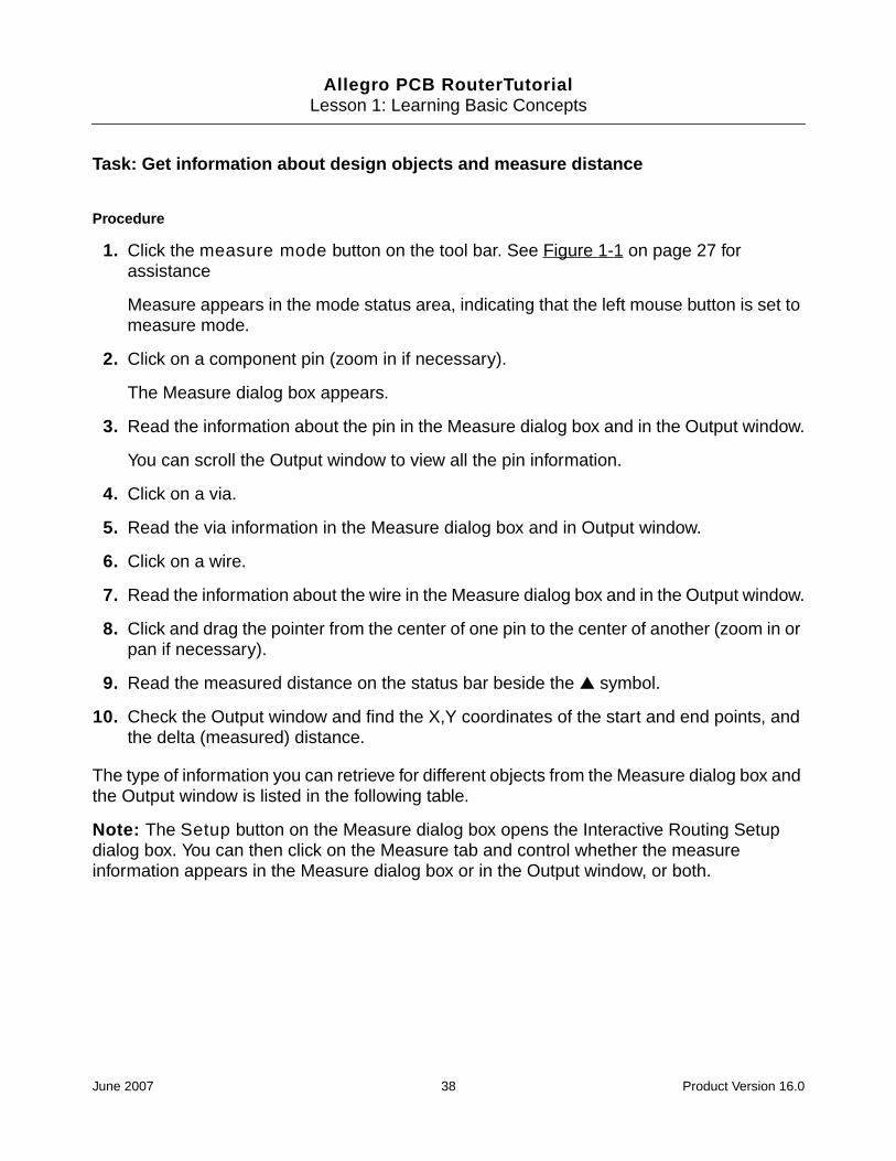
Task: Get information about design objects and measure distance
Procedure
1. Click the measure mode button on the tool bar. See Figure 1-1 on page 27 forassistance
Measure appears in the mode status area, indicating that the left mouse button is set tomeasure mode.
2. Click on a component pin (zoom in if necessary).
The Measure dialog box appears.
3. Read the information about the pin in the Measure dialog box and in the Output window.
You can scroll the Output window to view all the pin information.
4. Click on a via.
5. Read the via information in the Measure dialog box and in Output window.
6. Click on a wire.
7. Read the information about the wire in the Measure dialog box and in the Output window.
8. Click and drag the pointer from the center of one pin to the center of another (zoom in orpan if necessary).
9. Read the measured distance on the status bar beside the ▲ symbol.
10. Check the Output window and find the X,Y coordinates of the start and end points, andthe delta (measured) distance.
The type of information you can retrieve for different objects from the Measure dialog box andthe Output window is listed in the following table.
Note: The Setup button on the Measure dialog box opens the Interactive Routing Setupdialog box. You can then click on the Measure tab and control whether the measureinformation appears in the Measure dialog box or in the Output window, or both.
June 2007 38 Product Version 16.0

Allegro PCB RouterTutorialLesson 1: Learning Basic Concepts
Table 1-1 Objects and Related Information
When you click on this object . . . You get this information
component Pointer’s X,Y locationCurrent measurement unitsComponent outline dimensions (boundingrectangle)Layer locationReference designatorImage nameX,Y location in working unitsX,Y location in DBUDegrees of rotation
SMD pin Pointer’s X,Y locationCurrent measurement unitsBounding rectangle for the pin and its layerlocationComponent reference designator and imagenameComponent location (in both measurement unitsand DBU)Component side location and rotationPadstack id for the pinPadstack shape description and layer locationComponent pin idName of attached net
through-pin Pointer’s X,Y locationCurrent measurement unitsBounding rectangle for the pinComponent reference designator and imagenameComponent X,Y location (in both measurementunits and DBU)Layer location of componentComponent X,Y locationPin idPadstack id for the pinPadstack shape descriptions by layer includingdimensionsName of attached net
June 2007 39 Product Version 16.0

Allegro PCB RouterTutorialLesson 1: Learning Basic Concepts
via Pointer’s X,Y locationCurrent measurement unitsPadstack id for the viaPadstack shape descriptions by layerincluding dimensionsName of attached netWire path coordinatesWidth and layer locations of attached wiresegments
wire segment Pointer’s X,Y locationCurrent measurement unitsPath coordinatesWidth and layer location of the segmentName of attached net
When you click on this object . . . You get this information
June 2007 40 Product Version 16.0

Allegro PCB RouterTutorialLesson 1: Learning Basic Concepts
Saving Your Work
Before you end an autrouting session, you can save your work in a Session file, Placementfile, or Routes file. The following table explains the differences between these files.
Table 1-2 File Differences
In the following procedure, you save a Routes file and a Session file. You usually need to saveonly one file. However, both procedures are included so you can become familiar with eachprocedure.
A Session file... A Placement file... A Routes file...
Contains placement and route dataand a pointer to the original designfile. After you create a session file,you can start the autorouter and loadthe session file instead of theoriginal design file. When theautorouter reads a session file, itloads the original design file and theroute and placement data from thesession file.
Contains placement dataonly. When you start theautorouter and load aplacement file, you mustspecify the originaldesign file.
Contains route data only.When you start theautorouter and load aroutes file, you mustspecify the originaldesign file.
Can be loaded only when you startthe autorouter.
Can be loaded when youstart the autorouter andafter it’s running.
Can be loaded when youstart the autorouter andafter it’s running.
Can be used in all layout systems tomerge the autorouting placementand routing data into the layout.
Can be used in mostlayout systems to mergethe autoroutingplacement data into thelayout.
Can be used in mostlayout systems to mergethe route data into thelayout.
Links a design file with specific routedata from a particular session. Thesession file is useful for managingdesign revisions because, it links theoriginal design file with the routedata for a particular session.
June 2007 41 Product Version 16.0

Allegro PCB RouterTutorialLesson 1: Learning Basic Concepts
Task: Save your work and exit the autorouter
Procedure
1. Choose File – Write – Routes.
The Write Routes dialog box opens.
On a Windows platform, the path to the tutorial directory and the filenamelesson1.rte appear in the data entry box, as shown in the following figure.
On a UNIX platform, the path and /lesson1.rte appear in the data entry box.
2. Click OK.
You created a Routes file. You could create a Session file using File – Write – Session,but you will create a Session file when you exit the autorouter.
3. Choose File – Quit.
The Save And Quit dialog box opens, as shown in the following figure.
On a Windows platform, the path to the tutorial directory and the file lesson1.ses appearin the data entry box.
On a UNIX platform, the path and /lesson1.ses appear in the data entry box.
4. Make sure Delete Did File is not checked.
June 2007 42 Product Version 16.0
Allegro PCB RouterTutorialLesson 1: Learning Basic Concepts
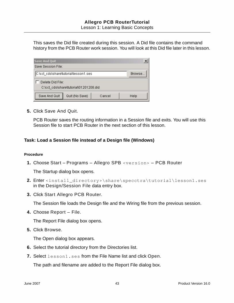
This saves the Did file created during this session. A Did file contains the commandhistory from the PCB Router work session. You will look at this Did file later in this lesson.
5. Click Save And Quit.
PCB Router saves the routing information in a Session file and exits. You will use thisSession file to start PCB Router in the next section of this lesson.
Task: Load a Session file instead of a Design file (Windows)
Procedure
1. Choose Start – Programs – Allegro SPB <version> – PCB Router
The Startup dialog box opens.
2. Enter <install_directory>\share\specctra\tutorial\lesson1.sesin the Design/Session File data entry box.
3. Click Start Allegro PCB Router.
The Session file loads the Design file and the Wiring file from the previous session.
4. Choose Report – File.
The Report File dialog box opens.
5. Click Browse.
The Open dialog box appears.
6. Select the tutorial directory from the Directories list.
7. Select lesson1.ses from the File Name list and click Open.
The path and filename are added to the Report File dialog box.
June 2007 43 Product Version 16.0
Allegro PCB RouterTutorialLesson 1: Learning Basic Concepts
8. Click OK.
A report window displays the Session file.
9. Browse the Session file and locate the following:
❑ Name of the Session file (lesson1.ses)
❑ Name of the original Design file (lesson1.dsn)
❑ Date and time the file was created
❑ Section of the Session file that contains the route data (located below thenetwork_out statement)
10. Close the Session file.
11. Choose File – Quit.
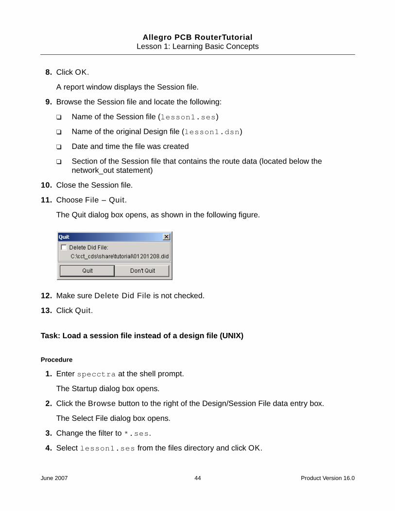
The Quit dialog box opens, as shown in the following figure.
12. Make sure Delete Did File is not checked.
13. Click Quit.
Task: Load a session file instead of a design file (UNIX)
Procedure
1. Enter specctra at the shell prompt.
The Startup dialog box opens.
2. Click the Browse button to the right of the Design/Session File data entry box.
The Select File dialog box opens.
3. Change the filter to *.ses.
4. Select lesson1.ses from the files directory and click OK.
June 2007 44 Product Version 16.0

Allegro PCB RouterTutorialLesson 1: Learning Basic Concepts
5. Click Start Allegro PCB Router
The Session file is loaded with the wiring from the previous session.
6. Choose Report – File.
The Report File dialog box opens.
7. Click the Browse button and select lesson1.ses from the Files directory.
8. Click OK from the Report File dialog box.
A report window opens and displays the Session file.
9. Browse the Session file and locate the following:
❑ Name of the session file (lesson1.ses)
❑ Name of the original Design file (lesson1.dsn)
❑ Date and time the file was created
❑ Section of the Session file that contains the route data
10. Close the Session file.
11. Click File – Quit.
The Quit dialog box opens, as shown in the following figure.
12. Make sure Delete Did File is not checked.
13. Click Quit.
June 2007 45 Product Version 16.0

Allegro PCB RouterTutorialLesson 1: Learning Basic Concepts
Reviewing Session Command History
PCB Router creates a command history file for each session. This command history file iscalled a Did file.
On Windows platforms, the Did file is created with an eight character, numeric filename thatderives from the month, day, hour, and minute when you start an autorouting session. Forexample, a Did file for a session you started June 15th at 11:45 is named 06151145.did.
On UNIX platforms, the Did file is created with a 10 character, numeric filename that derivesfrom the month, day, hour, minute, and seconds when you start an autorouting session. Forexample, a Did file for a session you started June 15th at 11:45:20 is named0615114520.did.
The following is an example of a Did file.
# Cadence Design Systems, Inc.
# PCB Router Automatic Router
# PCB ROuter Version V15.5 made 02/10/24 at 14:08:45
# Running on host 5540a1cf
#
# Command Line Parameters
# -----------------------
# Design File Name : ./lesson1.ses
# No "-do" or "-docmd" switches specified on command line.
# Colormap File Name : color.std
# FLEXlm License File Name : /usr/local/flexlm/licenses/license.dat
# Status File Name : ./monitor.sts
# Wires File Name : lesson1.w
#
#
report c:\specctra\tutorial\lesson1.ses
quit -c
Each time you start PCB Router, a new Did file is created. Together, the Status file, Did file,and Session file capture the routing status, command log, and routing data for the autoroutingsession.
Task: View the did file from your previous session (Windows)
Procedure
1. Start PCB Router and load lesson1.dsn.
June 2007 46 Product Version 16.0

Allegro PCB RouterTutorialLesson 1: Learning Basic Concepts
2. Choose Report – File.
The Report File dialog box opens.
3. Click Browse in the Report File dialog box.
The Open dialog box opens.
4. Scroll the Open dialog box and select the Did file from the previous session. The Did filefor the previous session is located just before the Did file for the current session. The lastDid file in the list is the one for the current session.
5. Open the Did file from the previous session.
The path and file are added in the Report File dialog box.
6. Click OK.
A report window displays the Did file.
7. Browse the Did file and verify the command history from the previous autoroutingsession.
8. Close the report.
9. Choose File – Quit.
The Quit dialog box opens.
10. Click Delete Did File to remove the Did file.
11. Click Quit.
PCB Router exits without saving a Session file or a Did file.
Task: View the did file from your previous session (UNIX)
Procedure
1. Start PCB Router and load lesson1.dsn.
2. Click Report – File.
The Report File dialog box opens.
3. Click Browse in the Report File dialog box.
The Select File dialog box opens.
June 2007 47 Product Version 16.0

Allegro PCB RouterTutorialLesson 1: Learning Basic Concepts
4. Select the Did file from the previous session. The Did file for the previous session islocated just before the Did file for the current session. The last Did file in the list is theone for the current session.
5. Click OK.
The path and filename are added in the Report File dialog box.
6. Click OK.
A report window displays the Did file.
7. Browse the Did file and verify the command history from the previous autoroutingsession.
8. Close the report.
9. Choose File – Quit.
The Quit dialog box opens.
10. Click Delete Did File to remove the Did file.
11. Click Quit.
PCB Router exits without saving a Session file or a Did file.
In Lesson 3, you will learn how to use a Did file to capture GUI commands and create acommand file (Do file) that you can run in PCB Router.
June 2007 48 Product Version 16.0
Allegro PCB RouterTutorialLesson 1: Learning Basic Concepts
What You Learned
In this lesson, you learned about the PCB Router’s user interface and how to perform basicdesign tasks.
You learned how to:
■ start the autorouter and load a design.
■ use the GUI to execute commands.
■ pan and zoom within in the Design window.
■ measure distance and get information about design objects.
■ save your work.
■ review a session's command history.
In the next lesson, you will learn how to place components interactively and automatically.
June 2007 49 Product Version 16.0

Allegro PCB RouterTutorialLesson 1: Learning Basic Concepts
June 2007 50 Product Version 16.0

Allegro PCB RouterTutorial
2Lesson 2: Placing Components
What You Will Learn
This lesson teaches you how to use PCB Router’s interactive and automatic placement tools.
In this lesson you will learn:
■ the basic steps for placing components.
■ how to set placement options.
■ how to set placement rules.
■ how to preplace connectors and other critical components.
■ how to place large components.
■ how to edit the placement.
■ how to place small components.
This lesson takes about 60 minutes to complete.
What to do Before You Begin
Before you begin this lesson, do the following:
■ Complete Lesson 1: Learning Basic Concepts.
Important
A PlaceBase license is required to complete the tasks in this lesson. For details onPCB Router licensing, products and features, refer to Chapter 1 of the Allegro PCBRouter User Guide.
June 2007 51 Product Version 16.0

Allegro PCB RouterTutorialLesson 2: Placing Components
Understanding the Basic Steps for Placing Components
Placing components consists of four basic steps.
■ Setting placement rules
■ Preplacing critical components
■ Placing large components
■ Placing small components
Figure 2-1 Basic Steps of Component Placement
In the first step, you set placement rules. During both automatic and interactive placement,the design is checked for rule violations.
In the second step, connectors and other position-critical components are preplaced andlocked in position using interactive placement tools.
In the third and fourth steps, components are placed and locations are optimized to reducemanhattan lengths and guide crossings. Large components are placed first and then smallcomponents.
June 2007 52 Product Version 16.0

Allegro PCB RouterTutorialLesson 2: Placing Components
Setting Placement Rules
PCB Router provides a comprehensive set of placement rules. Basic placement rules controlthe spacing between components, the orientation of components, and the sides on which theautorouter places components. More advanced rules control floor planning based on powerdissipation, power supply, and component height. In this lesson, you will set basic rules. Formore information on setting advanced placement rules, see the Placement online help.
Understanding the Rules Hierarchy
Placement rules can be specified at different levels and, consequently form a hierarchy. Rulesat higher levels in the hierarchy override rules at lower levels that are set for the same physicalobjects. For example, consider what happens if you set a global (PCB) spacing rule of .25inches for all components and a spacing rule of .8 inches for a specific connector. Theautorouter follows the .8 spacing rule only in the area surrounding the connector. Theautorouter follows the .25 spacing rule in the areas surrounding other components. Thecomponent-level spacing rule overrides the PCB-level spacing rule.
The following table shows the levels of hierarchy in which you can set rules and the order ofprecedence for all placement rule levels. Global placement rules (PCB rules) have the lowestprecedence, and image_image rules have the highest precedence.
Table 2-1 Rules Hierarchy
This rule level . . . Does this . . .
image_image Sets rules between images. An image is the footprint definitionof a component. This is the highest precedence rule.
family_family Sets rules between families. A family is a group of images.
room_image_set Sets rules for an image_set assigned to a room.
room Sets rules for a room, which is an area of the design in whichthe autorouter places specified components.
super cluster Sets rules for a super cluster, which is a group of componentsthat is treated as a single component.
component Sets rules for a component, which is an instance of an image.
image Sets rules for an image, which defines a component footprint.An image is the footprint definition of a component.
image_set Sets rules for images with the same type property. The typeproperties are large, small, capacitor, or discrete.
June 2007 53 Product Version 16.0
Allegro PCB RouterTutorialLesson 2: Placing Components
Note: The order of precedence is fixed and cannot be changed.
Setting a Placement Grid and Spacing Rule
Using the Placement Setup dialog box, you can set a placement grid and a PCB spacing rule.
PCB Router does not require that you define a grid for automatic placement, but if design ormanufacturing rules dictate a placement grid, you can set the grid for all components (SMDand through-pin) in the Placement Setup dialog box.
Note: You can set separate placement grids for SMD and through-pin components bychoosing Rules – PCB – Placement Grids.
In addition to setting the placement grid, you can use the Placement Setup dialog box to seta PCB spacing rule. A PCB spacing rule sets the minimum spacing allowed between allcomponents in the design. Rules are set at other levels through the Rules menu. In thefollowing procedure, you will set a PCB spacing rule of .05 inches.
Task: Set a placement grid and spacing rule
Procedure
1. Start PCB Router and load lesson2.dsn from the tutorial directory. See Where tofind the Accompanying Lesson Files on page 12 for the location of this directory.
When you first start PCB Router, you are in Route mode. The menu bar and status barare specific to autorouting. You need to change to Place mode.
2. Click the Place button on the tool bar.
The tool bar changes.
pcb Sets global rules for all components in the design. This is thelowest precedence rule.
This rule level . . . Does this . . .
June 2007 54 Product Version 16.0

Allegro PCB RouterTutorialLesson 2: Placing Components
Figure 2-2 Placement GUI (Windows)
3. Choose Autoplace – Setup.
The Placement Setup dialog box opens.
4. Enter .05 in the PCB Placement Grid data entry box.
5. Enter .05 in the PCB Placement Spacing data entry box.
Menu Bar
place mode
route mode
Status Bar
Messages
Tool Bar
CommandEntry
Command
Units
DesignWindow
Mode Status Design CoordinatesControl
measuremode
repaint
view alllayers
status
select componentmode
select component mode
lock component mode
move component mode
push component mode
pivot component mode
flip component mode
align component mode
June 2007 55 Product Version 16.0

Allegro PCB RouterTutorialLesson 2: Placing Components
The Placement Setup dialog box looks like the following.
6. Click OK.
You defined a grid of .05 inches and a spacing rule of .05 inches. Notice that the Checkingoption in the right side of the status area is selected. This option checks for placement ruleviolations while you interactively place components and prevents placing or moving acomponent if it violates a rule. If you want to place a component in a location that violates arule, turn off Checking.
Note: You can set separate spacing rules for SMD components, through-pin components,and between SMD and through-pin components by choosing Rules – PCB – Spacing. Youalso can use this command to see the current PCB spacing rule.
June 2007 56 Product Version 16.0

Allegro PCB RouterTutorialLesson 2: Placing Components
Preplacing Connectors and Critical Components
After you set placement rules, you are ready to preplace connectors and other criticalcomponents. In this stage of placing components, you will:
■ display the component reference designators.
■ place components by specifying XY locations.
■ place components from a defined list.
■ lock the preplaced components.
Displaying Component Reference Designators
In the following procedure, you turn on the reference designator labels so that you can identifycomponents.
Task: Display component reference designators
Procedure
1. Choose View – Labels.
The View Labels dialog box opens.
2. Make sure Ref Des is selected.
3. Make sure the Side is set to Both.
4. Click OK.
A reference designator label appears in the center of each component.
Note: The router scales the work area. If you do not see all the designator labels, youneed to zoom in to adjust the magnification of the work area.
Placing Components by Specifying X,Y Locations
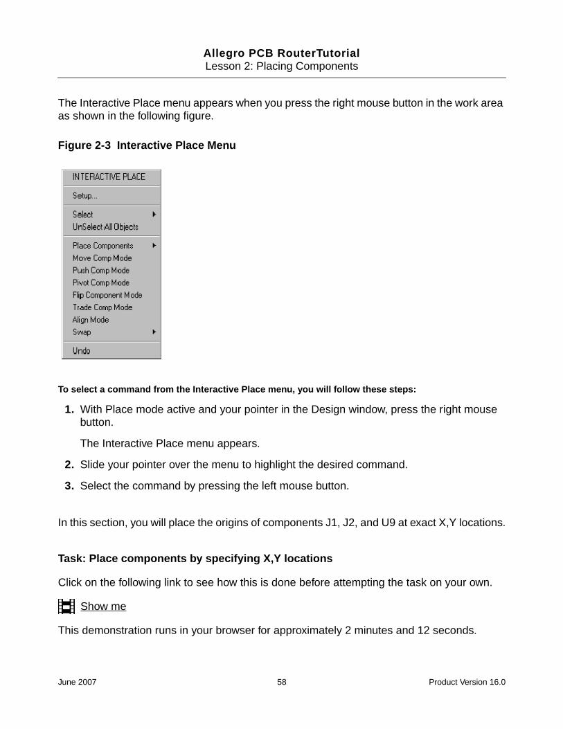
Through the Interactive Place menu, the autorouter offers a variety of ways to placecomponents interactively. You can place a single component, a list of components, andmultiple components. You can place components by specifying X,Y locations, by clicking apoint in the work area, or based on connectivity.
June 2007 57 Product Version 16.0
Allegro PCB RouterTutorialLesson 2: Placing Components
The Interactive Place menu appears when you press the right mouse button in the work areaas shown in the following figure.
Figure 2-3 Interactive Place Menu
To select a command from the Interactive Place menu, you will follow these steps:
1. With Place mode active and your pointer in the Design window, press the right mousebutton.
The Interactive Place menu appears.
2. Slide your pointer over the menu to highlight the desired command.
3. Select the command by pressing the left mouse button.
In this section, you will place the origins of components J1, J2, and U9 at exact X,Y locations.
Task: Place components by specifying X,Y locations
Click on the following link to see how this is done before attempting the task on your own.
Show me
This demonstration runs in your browser for approximately 2 minutes and 12 seconds.
June 2007 58 Product Version 16.0
Allegro PCB RouterTutorialLesson 2: Placing Components
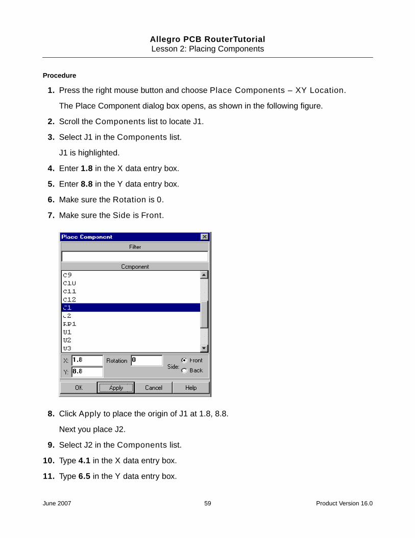
Procedure
1. Press the right mouse button and choose Place Components – XY Location.
The Place Component dialog box opens, as shown in the following figure.
2. Scroll the Components list to locate J1.
3. Select J1 in the Components list.
J1 is highlighted.
4. Enter 1.8 in the X data entry box.
5. Enter 8.8 in the Y data entry box.
6. Make sure the Rotation is 0.
7. Make sure the Side is Front.
8. Click Apply to place the origin of J1 at 1.8, 8.8.
Next you place J2.
9. Select J2 in the Components list.
10. Type 4.1 in the X data entry box.
11. Type 6.5 in the Y data entry box.
June 2007 59 Product Version 16.0
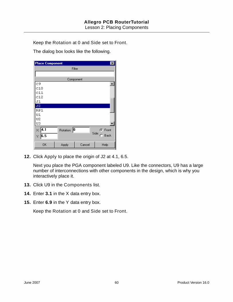
Allegro PCB RouterTutorialLesson 2: Placing Components
Keep the Rotation at 0 and Side set to Front.
The dialog box looks like the following.
12. Click Apply to place the origin of J2 at 4.1, 6.5.
Next you place the PGA component labeled U9. Like the connectors, U9 has a largenumber of interconnections with other components in the design, which is why youinteractively place it.
13. Click U9 in the Components list.
14. Enter 3.1 in the X data entry box.
15. Enter 6.9 in the Y data entry box.
Keep the Rotation at 0 and Side set to Front.
June 2007 60 Product Version 16.0

Allegro PCB RouterTutorialLesson 2: Placing Components
The dialog box looks like the following.
16. Click OK.
The design is shown in the following figure.
June 2007 61 Product Version 16.0

Allegro PCB RouterTutorialLesson 2: Placing Components
You just learned how to place components by specifying X,Y coordinates. Next you will learnhow to place a list of components.
Placing Components From a List
Using Place List mode, you can specify a list of components and place them in the order youspecify. The first component in the list attaches to the pointer. Drag the component to thelocation you want, and click the left mouse button to place it. Immediately, the next componentin the list attaches to the pointer so you can drag the component to the location you want andclick the left mouse button to place it. You repeat this process until all components in the listare placed.
Task: Place components from a list
Click on the following link to see how this is done before attempting the task on your own.
Show me
This demonstration runs in your browser for approximately 3 minutes and 50 seconds.
Procedure
1. Press the right mouse button and select Place Components – Place List Mode.
The Place Component List dialog box opens.
2. Select Ordered Components, which tells the autorouter to place the components in theorder that you specify in the Comp List.
3. Type the following in the Comp List data entry box:
c1 c2 c3 c4
Note: Make sure you leave a space between each reference designator.
June 2007 62 Product Version 16.0
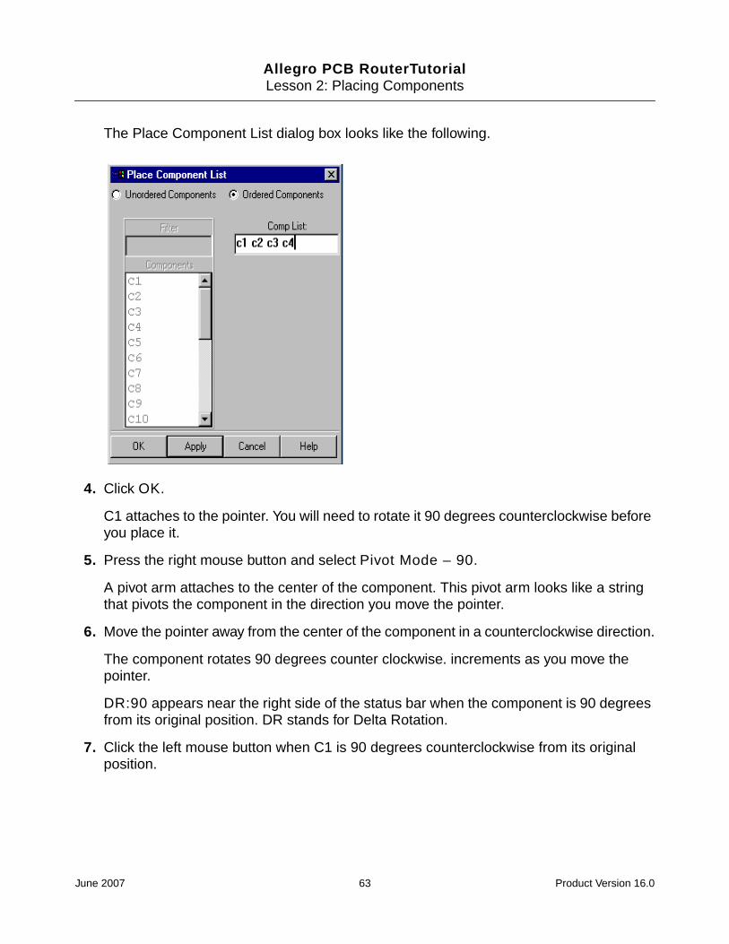
Allegro PCB RouterTutorialLesson 2: Placing Components
The Place Component List dialog box looks like the following.
4. Click OK.
C1 attaches to the pointer. You will need to rotate it 90 degrees counterclockwise beforeyou place it.
5. Press the right mouse button and select Pivot Mode – 90.
A pivot arm attaches to the center of the component. This pivot arm looks like a stringthat pivots the component in the direction you move the pointer.
6. Move the pointer away from the center of the component in a counterclockwise direction.
The component rotates 90 degrees counter clockwise. increments as you move thepointer.
DR:90 appears near the right side of the status bar when the component is 90 degreesfrom its original position. DR stands for Delta Rotation.
7. Click the left mouse button when C1 is 90 degrees counterclockwise from its originalposition.
June 2007 63 Product Version 16.0

Allegro PCB RouterTutorialLesson 2: Placing Components
You are ready to place C1. The following figure shows where to place C1 and C2.
8. Drag C1 to the left of J1 and click to place it.
You can use the middle mouse button for the following operations to pan or zoom to anew location.
C2 attaches to the pointer after you place C1.
9. Repeat steps 5 through 7 to rotate C2 90 degrees counterclockwise.
10. Drag C2 to the right of J1 and click to place it.
C3 attaches to the pointer.
11. Repeat steps 5 through 7 to rotate C3 90 degrees counterclockwise.
You are ready to place C3. The following figure shows where to place C3 and C4.
12. Drag C3 to the left of J2 and click to place it.
C4 attaches to the pointer.
13. Repeat steps 5 through 7 to rotate C4 90 degrees counterclockwise.
14. Drag C4 to the right of J2 and click to place it.
Note: If you do not like where you placed a component and you want to move it, pressthe right mouse button and select Move Component. Click the component, drag it to thenew location, and click to place it.
Next you will lock the preplaced components so the autorouter cannot move them duringautomatic and interactive placement.
June 2007 64 Product Version 16.0

Allegro PCB RouterTutorialLesson 2: Placing Components
Locking Components
After you place critical components, you lock them in position so PCB Router does not movethem during automatic or interactive placement. If you need to move a component at a latertime, you can unlock it, move it, and lock it again.
Task: Lock critical components
Procedure
1. Click the Lock button on the tool bar.
Lock Position appears in the mode status area.
2. Click a point to the left of C1.
3. Drag the pointer diagonally around C1, J1, and C2, and release the left mouse buttonwhen the bounding box encloses the components.
The locked components display a magenta border. Magenta is the default locked color.
4. Repeat steps 2 and 3 to lock components C3, J2, and C4.
Note: You can unlock the components while you are in Lock Position mode. To unlock thecomponents, click on each locked component or draw a bounding box around thecomponents. You also can use Edit – [Un]Lock Components and Edit – [Un]LockComponents Mode to lock and unlock components.
June 2007 65 Product Version 16.0

Allegro PCB RouterTutorialLesson 2: Placing Components
Placing Large Components
PCB Router assigns the large and small properties to components based on the number ofpins. A large component contains four or more pins. A small component contains three or lesspins. PCB Router usually places large components with the highest connectivity first.
In this section you will:
■ define areas where you do not want components placed.
■ automatically place large components.
■ interchange placed components to reduce manhattan lengths, minimize crossovers, andreduce congestion.
Defining Areas where PCB Router Cannot Place Components
Before you automatically place the large components, you need to provide routing spacearound the connectors. To do this, you specify an area around each connector where the PCBRoutercannot place components. These areas are called placement keepout areas.
Task: Define placement keepout areas
Procedure
1. Choose Define – Keepout – Draw Mode.
Draw Keepout appears in the mode status area. You will draw a bounding box as closeas possible to C1, J1, and C2.
2. Click a point to the lower left of C1.
3. Drag the pointer diagonally around C1, J1, and C2, and release the left mouse buttonwhen the bounding box encloses the components. If you do not like how you drew thebox, choose Define – Keepout – Draw Mode to remove the box and start with step 2to draw a new bounding box.
June 2007 66 Product Version 16.0
Allegro PCB RouterTutorialLesson 2: Placing Components
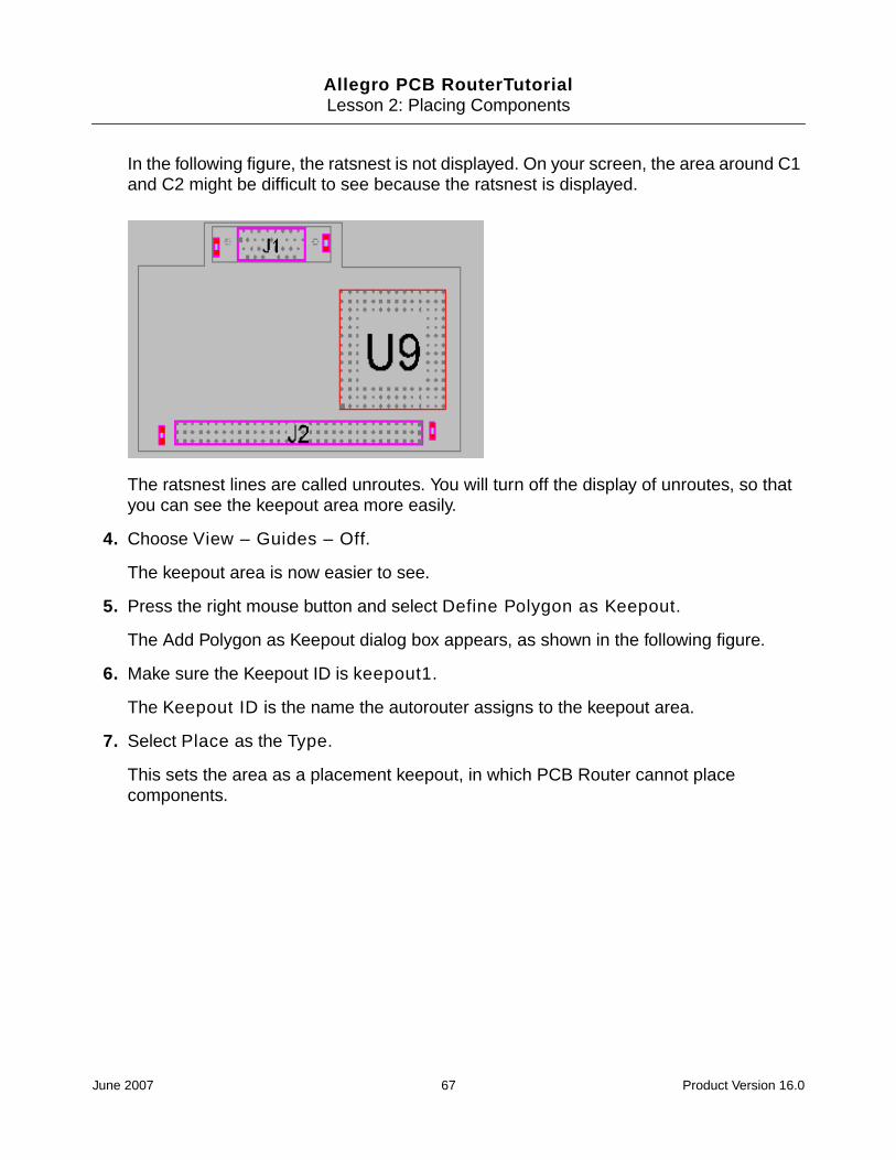
In the following figure, the ratsnest is not displayed. On your screen, the area around C1and C2 might be difficult to see because the ratsnest is displayed.
The ratsnest lines are called unroutes. You will turn off the display of unroutes, so thatyou can see the keepout area more easily.
4. Choose View – Guides – Off.
The keepout area is now easier to see.
5. Press the right mouse button and select Define Polygon as Keepout.
The Add Polygon as Keepout dialog box appears, as shown in the following figure.
6. Make sure the Keepout ID is keepout1.
The Keepout ID is the name the autorouter assigns to the keepout area.
7. Select Place as the Type.
This sets the area as a placement keepout, in which PCB Router cannot placecomponents.
June 2007 67 Product Version 16.0

Allegro PCB RouterTutorialLesson 2: Placing Components
The Add Polygon As Keepout dialog box looks like the following.
8. Click OK.
The keepout area appears as a bounding box filled with a crosshatched pattern.
Note: Information about keepouts will display in the measure box and output window ifthe object selection button is turned on in the layers panel next to the keepout button.
Next you create a keepout area around C3, J2, and C4.
9. Make sure Draw Keepout mode is still set by checking the mode status area.
10. Click a point to the lower left of C3.
11. Drag the pointer diagonally around C3, J2, and C4, and release the left mouse buttonwhen the bounding box encloses the components. Remember to draw the boundary boxas close as possible to the components.
12. Press the right mouse button and select Define Polygon as Keepout.
The Add Polygon as Keepout dialog box opens.
13. Make sure the Keepout ID is keepout2 and Place is selected.
14. Click OK.
June 2007 68 Product Version 16.0

Allegro PCB RouterTutorialLesson 2: Placing Components
The keepout areas appear as crosshatched rectangles, as shown in the following figure.
Next you will automatically place the large components. First, display the unroutes so youcan see the connectivity while the autorouter places the components.
15. Choose View – Guides – All.
The guides display.
Note: To create a keepout area by entering coordinates, choose Define – Keepout –By Coordinates.
Automatically Placing Large Components
You initially place ICs and other large components by using the InitPlace Large Componentsdialog box. You use the dialog box to control the preferred component spacing, placementside, and component orientations.
These preferences are not rules. Preferences set in the InitPlace Large Components dialogbox are followed if they do not violate placement rules.
You will place the large SMD components on the front side with a vertical orientation and thePTH component (RP1) on the front side with a horizontal orientation.
Task: Automatically place large components
Procedure
1. Choose Autoplace – InitPlace Large Components.
The InitPlace Large Components dialog box opens, as shown in the following figure.
June 2007 69 Product Version 16.0
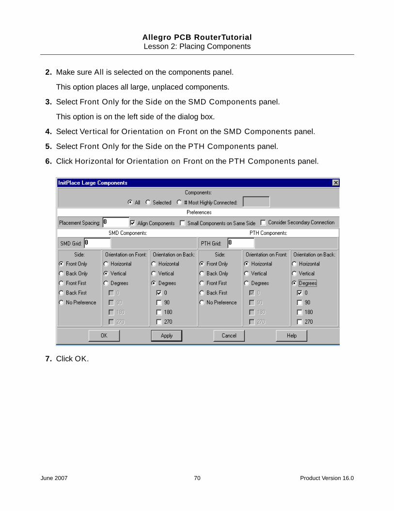
Allegro PCB RouterTutorialLesson 2: Placing Components
2. Make sure All is selected on the components panel.
This option places all large, unplaced components.
3. Select Front Only for the Side on the SMD Components panel.
This option is on the left side of the dialog box.
4. Select Vertical for Orientation on Front on the SMD Components panel.
5. Select Front Only for the Side on the PTH Components panel.
6. Click Horizontal for Orientation on Front on the PTH Components panel.
7. Click OK.
June 2007 70 Product Version 16.0
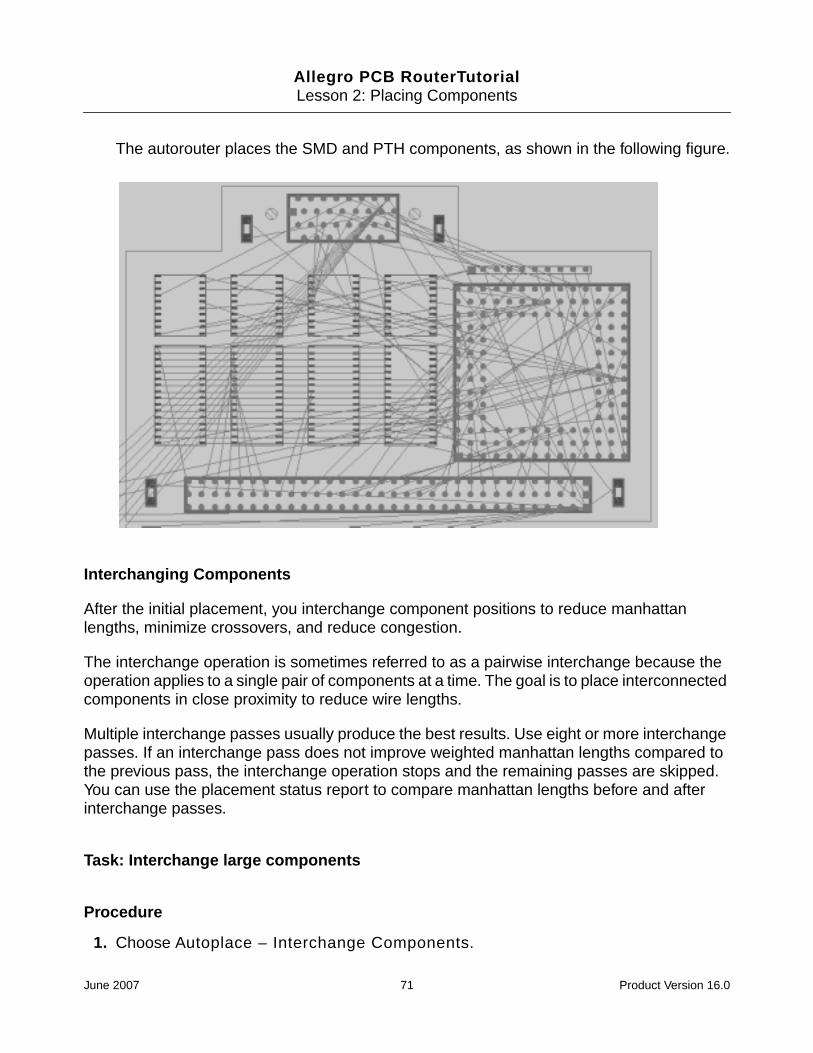
Allegro PCB RouterTutorialLesson 2: Placing Components
The autorouter places the SMD and PTH components, as shown in the following figure.
Interchanging Components
After the initial placement, you interchange component positions to reduce manhattanlengths, minimize crossovers, and reduce congestion.
The interchange operation is sometimes referred to as a pairwise interchange because theoperation applies to a single pair of components at a time. The goal is to place interconnectedcomponents in close proximity to reduce wire lengths.
Multiple interchange passes usually produce the best results. Use eight or more interchangepasses. If an interchange pass does not improve weighted manhattan lengths compared tothe previous pass, the interchange operation stops and the remaining passes are skipped.You can use the placement status report to compare manhattan lengths before and afterinterchange passes.
Task: Interchange large components
Procedure
1. Choose Autoplace – Interchange Components.
June 2007 71 Product Version 16.0

Allegro PCB RouterTutorialLesson 2: Placing Components
The Interchange Components dialog box appears.
2. Make sure Large is selected.
3. Make sure 8 is in the value for Passes.
The Interchange Components dialog box looks like the following.
4. Click OK.
After each component interchange, the work area is repainted because DisplayExchange in the dialog box was selected. This button controls whether graphics areupdated with each component interchange. To improve performance with larger designs,you unselect Display Exchange.
5. Choose File – Quit.
The Save and Quit dialog box opens, as shown in the following figure.
June 2007 72 Product Version 16.0

Allegro PCB RouterTutorialLesson 2: Placing Components
6. Click Delete Did File to remove the did file.
7. Click Quit (No Save) to exit without saving a session file and Did file.
Next you will learn to interactively align components.
Aligning Components
You can align components by using Align Comp mode. In this mode, you select thecomponents you want to move, then you select a reference component to which thesecomponents align.
Figure 2-4 Component Alignment
June 2007 73 Product Version 16.0

Allegro PCB RouterTutorialLesson 2: Placing Components
If Checking is on and the alignment causes a placement violation, PCB Router does not aligncomponents. If you want to ignore rule violations, turn off Checking in the status bar. You’llleave Checking on in the following procedure.
Task: Align components
Procedure
1. Start PCB Router and load lesson2.dsn from the tutorial directory.
You need to change to Place mode.
2. Click the Placement button on the tool bar.
You will load a placement file.
3. Choose File – Read – Placement.
The Read Placement dialog box opens.
4. Click the Browse button.
The Open dialog box appears for Windows platforms.
The Select File dialog box appears for UNIX platforms.
5. Change to the tutorial directory for Windows platforms and open lesson2.plc.
Make sure lesson2.plc is selected and click OK for UNIX platforms.
The filename is added in the Read Placement dialog box.
6. Click OK.
June 2007 74 Product Version 16.0

Allegro PCB RouterTutorialLesson 2: Placing Components
The Placement file loads. The Small Outline Integrated Circuits (SOICs) are not aligned,as shown in the following figure.
7. Choose View – Guides – Off to turn off the guides.
You will align the SOICs.
8. Press the right mouse button and select Align Mode.
Align Comp appears in the mode status area.
You will use the right SOIC as the reference component to align the three SOICs.
9. Drag the pointer to enclose the three 32-pin SOICs that are located on the left as shownin the previous figure.
The three SOICs are selected. You will align these SOICs to the 32-pin SOIC that islocated on the right.
10. Click in the 32-pin SOIC that is located on the right.
June 2007 75 Product Version 16.0

Allegro PCB RouterTutorialLesson 2: Placing Components
The components align, as shown in the following figure.
Next you will align the three 20-pin SOICs that are located above the 32-pin SOICs asshown in the previous figure. Align Comp mode is still active.
11. Drag the pointer to enclose the three 20-pin SOICs that are located on the left.
The three SOICs are selected. You will align these SOICs to the reference 20-pin SOICcomponent that is located on the right.
12. Click in the 20-pin SOIC that is located on the right.
June 2007 76 Product Version 16.0

Allegro PCB RouterTutorialLesson 2: Placing Components
The components align, as shown in the following figure.
Note: PCB Router uses a reference point on each component to make the alignment. In theprevious procedure, the alignment was relative to the upper left pin of the referencecomponent, which is the default. You can change this reference point by using the PlacementSetup dialog box.
June 2007 77 Product Version 16.0

Allegro PCB RouterTutorialLesson 2: Placing Components
Placing Small Components
You can place small signal components by choosing Autoplace – InitPlace SmallComponents. To place decoupling capacitors, you will use another method.
PCB Router can learn a component pattern, which is the side, location, and orientation of asmall component relative to a large component. This component pattern is applied by placingother instances of the small component image in the same pattern to other instances of thelarge component image.
In this section, you will place the capacitors by having PCB Router learn and applycomponent patterns.
You will complete the following tasks
■ Display power pin labels
■ Move, flip, and pivot a capacitor
■ Learn the component pattern
■ Apply the component pattern to other instances of the large component image
Displaying Power Pin Labels
You will need to display the power pin labels to orient the components. To display the powerpins, turn on the power pins layer.
Task: Display power pins labels
Procedure
1. Click the Layer button on the tool bar.
The Layers panel appears. The Layers panel controls layer visibility, layer routingdirection, and layer selection.
2. Click Power pins on the Layers panel. Power pins is located near the bottom of the Layerpanel.
The power pins display.
3. Click Close on the Layers.
June 2007 78 Product Version 16.0

Allegro PCB RouterTutorialLesson 2: Placing Components
Now that you can see the power pins, you will move C5 (on the PCB bottom side) so that thepower pin of C5 is under the power pin of U1 (on the PCB top side).
Moving, Flipping, and Pivoting a Component
An easy way to place a component is to use Move Comp mode. When you click on acomponent in this mode, the component's reference designator displays. As you move thepointer, a ghost image of the component follows. The next click places the component at thelocation under the pointer.
You will need to display the reference designators, which appear at component centers.
Task: Move, flip, and pivot a component
Procedure
1. Choose View – Labels.
The View Labels dialog box opens.
2. Make sure Ref Des is selected.
3. Click OK.
4. Press the right mouse button and select Move Comp Mode.
Move Comp appears in the mode status area.
5. Click on C5, which is the bottom component in the column of unplaced components. Youcan use the middle mouse button to zoom in if necessary.
The component attaches to the pointer. You need to flip the component to the back sideby using the Move Comp menu.
6. Press the right mouse button and select Flip from the Move Comp menu.
This menu contains commands that manipulate the component before you place it.
Next you need to pivot the component so that the power pin is at the bottom of thecomponent, as shown in the following figure.
June 2007 79 Product Version 16.0
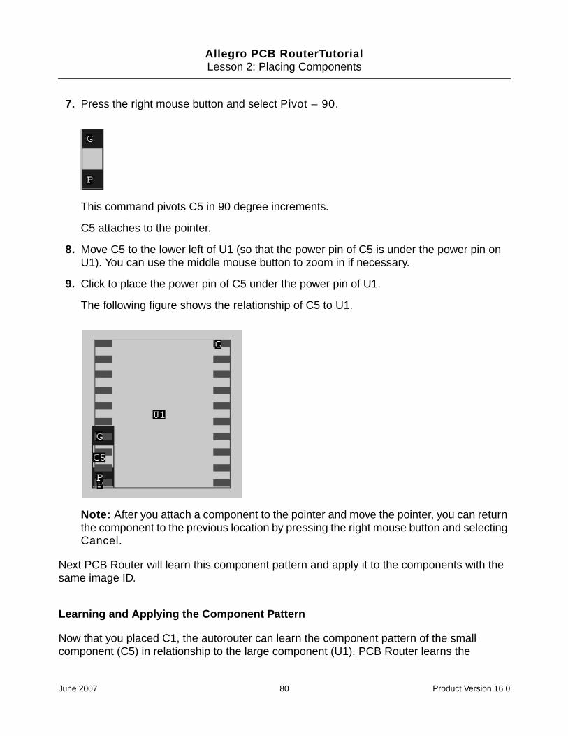
Allegro PCB RouterTutorialLesson 2: Placing Components
7. Press the right mouse button and select Pivot – 90.
This command pivots C5 in 90 degree increments.
C5 attaches to the pointer.
8. Move C5 to the lower left of U1 (so that the power pin of C5 is under the power pin onU1). You can use the middle mouse button to zoom in if necessary.
9. Click to place the power pin of C5 under the power pin of U1.
The following figure shows the relationship of C5 to U1.
Note: After you attach a component to the pointer and move the pointer, you can returnthe component to the previous location by pressing the right mouse button and selectingCancel.
Next PCB Router will learn this component pattern and apply it to the components with thesame image ID.
Learning and Applying the Component Pattern
Now that you placed C1, the autorouter can learn the component pattern of the smallcomponent (C5) in relationship to the large component (U1). PCB Router learns the
June 2007 80 Product Version 16.0
Allegro PCB RouterTutorialLesson 2: Placing Components
orientation, location, and side of the small component with respect to the large component. Itthen places other instances of the capacitor image in the same pattern to other instances ofthe SOIC image.
Task: Learn and apply the component pattern
Procedure
1. Click the Select Comp button on the tool bar.
Sel Comp appears in the mode status area.
2. Drag the pointer to enclose U1 and C5.
The two components are selected and Selected:2 appears in the status area.
3. Choose Autoplace – Small Comp Pattern – Learn.
PCB Router stores orientation, location, and side information about the relationshipbetween C5 and U1.
4. Unselect C5 and U1 by dragging the pointer over them.
5. Choose Select – Images – Sel Image Mode.
Sel Image appears in the mode status area. Using this mode, you can select all instancesof an image by clicking on one instance.
6. Click on U1.
U1, U2, U3, and U4 are selected.
7. Choose Autoplace – Small Comp Pattern – Apply to Selected.
The learned pattern is applied, and the power pins of C6, C7, and C8 are placed underthe power pins on U2, U3, and U4.
8. Choose Select – UnSelect All Placement Objects.
Next you place the power pins of C9, C10, C11, and C12 under the power pins of U5,U6, U7, and U8 by repeating the steps from the previous section.
9. Press the right mouse button and select Move Comp Mode.
You will move the power pin of C9 under the power pin of U8.
10. Click on C9.
You need to flip C9 to the back side.
June 2007 81 Product Version 16.0

Allegro PCB RouterTutorialLesson 2: Placing Components
11. Press the right mouse button and select Flip.
Next you pivot C9 so that the power pin is at the top.
12. Press the right mouse button and select Pivot – 90.
13. Move C9 to the upper right of U8 (so that the power pin of C9 is under the power pin onU8).
14. Click to place the power pin of C9 under the power pin of U8.
The following figure shows the relationship of C9 to U8.
Next you will learn and apply this component pattern to the unplaced capacitors.
15. Click the Select Comp button on the tool bar.
Sel Comp appears in the mode status area.
16. Select U8 and C9 by dragging the pointer over them and releasing the left mouse button.
The two components are selected, and Selected:2 appears in the status area.
17. Choose Autoplace – Small Comp Pattern – Learn.
PCB Router stores orientation, location, and side information about the relationshipbetween C9 and U8.
18. Unselect C9 and U8 by dragging the pointer over them.
19. Choose Select – Images – Sel Image Mode.
June 2007 82 Product Version 16.0

Allegro PCB RouterTutorialLesson 2: Placing Components
20. Click on U8.
U5, U6, U7, and U8 are selected.
21. Choose Autoplace – Small Comp Pattern – Apply to Selected.
The learned pattern is applied, and the power pins of C10, C11, and C12 are placedunder the power pins of U5, U6, and U7.
22. Choose Select – UnSelect All Placement Objects.
Congratulations! All components are placed.
Quitting the Autorouter and Saving Placement Results
When you are satisfied with your placement results, save your work. You can save your workin a Placement file or a Session file. If you save a Placement file, you can reload the file atthe start of a session or anytime during the session. The Placement file is useful if you wantto perform multiple placement trials and compare the files to choose the best result. Youcreate a placement file by choosing File – Write – Placement.
If you create a Session file, you load the Session file only when you start PCB Router. Asession file contains a reference to the original design filename as well as detailed placement,floorplan, swap, netlist, and route data. You will exit PCB Router and create a Session file inthe next procedure.
Task: Quit the Autorouter and save a Session file
Procedure
1. Choose File – Quit.
The Save And Quit dialog box appears with lesson2.ses in the Save Session Filedata entry box, as shown in the following figure.
2. Click Delete Did File to remove the Did file.
June 2007 83 Product Version 16.0

Allegro PCB RouterTutorialLesson 2: Placing Components
In Lesson 1, you learned that a did file contains the command history from a theautorouter session. You do not need this file for the sesssion, so you will delete it.
3. Click Save and Quit.
PCB Router exits and saves the placement information in the Session file.
What You Learned
In this lesson, you learned how to place components interactively and automatically.
You learned :
■ the basic steps used in placing components.
■ how to set placement options.
■ how to set placement rules.
■ how to preplace connectors and critical components.
■ how to place large components.
■ how to edit the placement.
■ how to place small components.
In the next lesson, you will learn how to autoroute a PCB design.
June 2007 84 Product Version 16.0
Allegro PCB RouterTutorial
3Lesson 3: Routing a PCB Design
What You Will Learn
This lesson teaches you how to get the best results from the autorouter. In this lesson, youwill learn how the autorouter works and how to:
■ set routing rules.
■ use a Do file.
■ monitor autorouting progress.
This lesson takes about 90 minutes to complete.
What to do Before You Begin
Before you begin this lesson, do the following:
■ Complete Lesson 1: Learning Basic Concepts.
Note: You do not need to complete Lesson 2: Placing Components but you should readthrough the lesson to understand the automatic and interactive placement tools function.
June 2007 85 Product Version 16.0
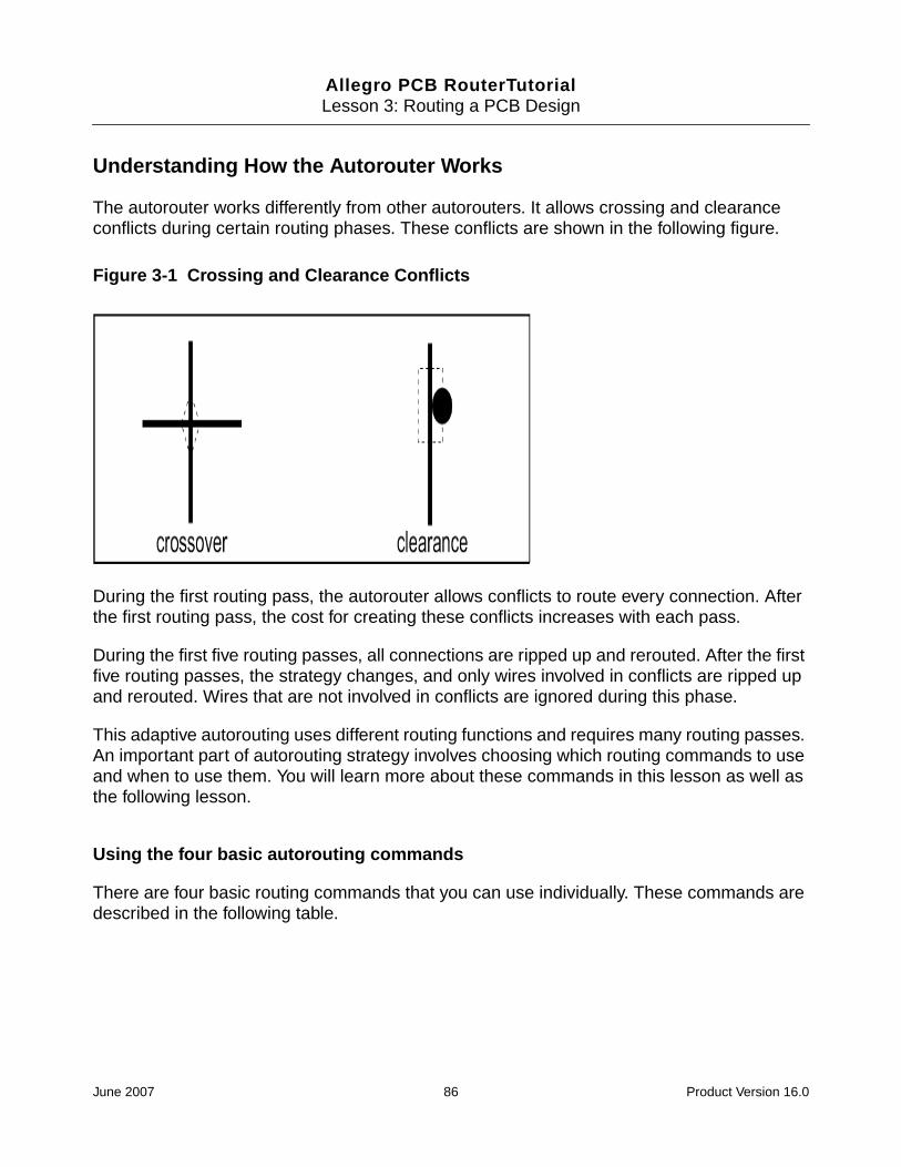
Allegro PCB RouterTutorialLesson 3: Routing a PCB Design
Understanding How the Autorouter Works
The autorouter works differently from other autorouters. It allows crossing and clearanceconflicts during certain routing phases. These conflicts are shown in the following figure.
Figure 3-1 Crossing and Clearance Conflicts
During the first routing pass, the autorouter allows conflicts to route every connection. Afterthe first routing pass, the cost for creating these conflicts increases with each pass.
During the first five routing passes, all connections are ripped up and rerouted. After the firstfive routing passes, the strategy changes, and only wires involved in conflicts are ripped upand rerouted. Wires that are not involved in conflicts are ignored during this phase.
This adaptive autorouting uses different routing functions and requires many routing passes.An important part of autorouting strategy involves choosing which routing commands to useand when to use them. You will learn more about these commands in this lesson as well asthe following lesson.
Using the four basic autorouting commands
There are four basic routing commands that you can use individually. These commands aredescribed in the following table.
June 2007 86 Product Version 16.0

Allegro PCB RouterTutorialLesson 3: Routing a PCB Design
Task: Perform Basic Autorouting
Click on the following link to see how this is done before attempting the task on your own.
Show me
This demonstration runs in your browser for approximately 3 minutes and 47seconds.
Procedure
1. Start PCB Router and load lesson3.dsn from the tutorial directory. See Where tofind the Accompanying Lesson Files on page 12 for the location of this directory.
You will route pins that share the same X or Y coordinate.
2. Choose Autoroute – Pre Route – Bus Routing.
The AutoRoute Bus Routing dialog box opens.
3. Make sure the Diagonal routing option is selected, as shown in the following figure.
Command Description
bus Routes pins that share the same X or Y coordinate. Thiscommand is useful for rerouting memory arrays, backplanes,and other pins that share a common X or Y corrdinate.
fanout Escapes SMD pads and through-pins to a via.
route Routes with conflicts, and after the first five passes, reroutesonly connections involved in conflicts. Escapes SMD pads tovias as needed.
clean Rips up and reroutes all connections. Adding new conflicts isprohibited.
June 2007 87 Product Version 16.0
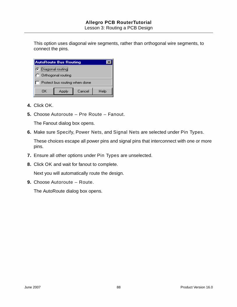
Allegro PCB RouterTutorialLesson 3: Routing a PCB Design
This option uses diagonal wire segments, rather than orthogonal wire segments, toconnect the pins.
4. Click OK.
5. Choose Autoroute – Pre Route – Fanout.
The Fanout dialog box opens.
6. Make sure Specify, Power Nets, and Signal Nets are selected under Pin Types.
These choices escape all power pins and signal pins that interconnect with one or morepins.
7. Ensure all other options under Pin Types are unselected.
8. Click OK and wait for fanout to complete.
Next you will automatically route the design.
9. Choose Autoroute – Route.
The AutoRoute dialog box opens.
June 2007 88 Product Version 16.0
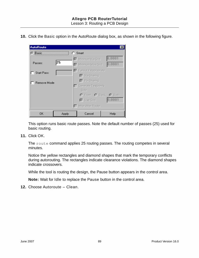
Allegro PCB RouterTutorialLesson 3: Routing a PCB Design
10. Click the Basic option in the AutoRoute dialog box, as shown in the following figure.
This option runs basic route passes. Note the default number of passes (25) used forbasic routing.
11. Click OK.
The route command applies 25 routing passes. The routing competes in severalminutes.
Notice the yellow rectangles and diamond shapes that mark the temporary conflictsduring autorouting. The rectangles indicate clearance violations. The diamond shapesindicate crossovers.
While the tool is routing the design, the Pause button appears in the control area.
Note: Wait for Idle to replace the Pause button in the control area.
12. Choose Autoroute – Clean.
June 2007 89 Product Version 16.0

Allegro PCB RouterTutorialLesson 3: Routing a PCB Design
The Clean dialog box opens, as shown in the following figure.
The clean command rips up and reroutes all connections. This improvesmanufacturability by removing unnecessary vias and bends, reducing routed length, andchanging SMD entries and exits.
13. Click OK.
Wait for Idle to replace the Pause button in the control area.
14. Click the Status Report button on the tool bar.
15. View the report and determine the actual number of route passes used to route thedesign.
If routing completes before all route passes are used, the remaining route passes areskipped and the clean passes proceed.
16. Close the Status report.
17. Choose File – Quit.
The Save and Quit dialog box opens, as shown in the following figure.
18. Click Delete Did File to remove the Did file.
19. Click Quit (No Save) to exit the autorouter without saving a Session file and a Did file.
Note: Another way to exit the autorouter without saving a Session file is to enter quit
June 2007 90 Product Version 16.0
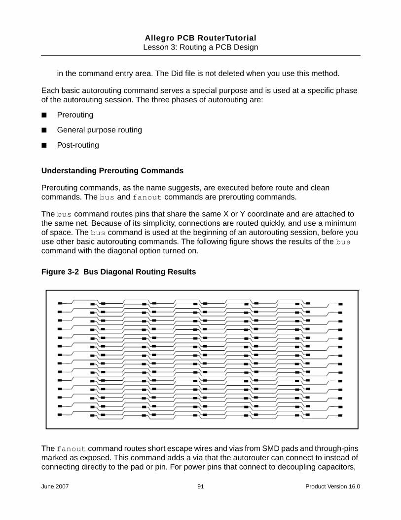
Allegro PCB RouterTutorialLesson 3: Routing a PCB Design
in the command entry area. The Did file is not deleted when you use this method.
Each basic autorouting command serves a special purpose and is used at a specific phaseof the autorouting session. The three phases of autorouting are:
■ Prerouting
■ General purpose routing
■ Post-routing
Understanding Prerouting Commands
Prerouting commands, as the name suggests, are executed before route and cleancommands. The bus and fanout commands are prerouting commands.
The bus command routes pins that share the same X or Y coordinate and are attached tothe same net. Because of its simplicity, connections are routed quickly, and use a minimumof space. The bus command is used at the beginning of an autorouting session, before youuse other basic autorouting commands. The following figure shows the results of the buscommand with the diagonal option turned on.
Figure 3-2 Bus Diagonal Routing Results
The fanout command routes short escape wires and vias from SMD pads and through-pinsmarked as exposed. This command adds a via that the autorouter can connect to instead ofconnecting directly to the pad or pin. For power pins that connect to decoupling capacitors,
June 2007 91 Product Version 16.0

Allegro PCB RouterTutorialLesson 3: Routing a PCB Design
you can control the fanout order by using the power_fanout rule. You can choose whetheryou want the escape wire to connect to the escape via first or the decoupling capacitor first.
The fanout command should follow the bus command but precede the route command.You can use fanout with up to five passes. Use multiple fanout passes with via and pinsharing enabled to optimize SMD escapes.
Understanding the General Purpose Routing Commands
The general purpose autorouting commands are route and clean. These commands canroute and reroute all connections in the design, except those routed by the bus command.
The route command uses costs that limit or control resources. These costs control thenumber of vias per connection, the number of conflicts per connection, and the distance thatwires can route on a layer in the wrong direction. The autorouter dynamically changes thesecosts over a series of route passes based on the routing history and the current wiringconditions. The following figure shows approximately when routing costs change during aseries of 25 route passes.
Figure 3-3 Costs Change During a Series of Route Passes
Because costs change during a series of route passes, you must specify a sufficient numberof passes. After pass five, only connections involved in conflicts are rerouted. If the wiringcompletes before all passes are used, the extra passes are skipped.
The clean command works differently from the route command. This command rips upand reroutes all connections (except those routed by the bus and fanout commands)instead of only the connections involved in conflicts.
June 2007 92 Product Version 16.0

Allegro PCB RouterTutorialLesson 3: Routing a PCB Design
The clean command is usually applied over two to four passes and should always follow aseries of route passes. Because clean rips up and reroutes all connections, tries to reroutethem using a different path, and does not add new conflicts, it usually completes moreconnections, reduces routing length and conflicts.
A typical sequence of basic autorouting commands is:
bus diagonalfanout 5route 25clean 2route 50 16clean 4
During clean passes, the built-in costs for vias and wrong-way routing are highest, thusimproving the quality of routing after each clean pass.
Note: In the typical sequence of basic autorouting commands, four clean passes areincluded at the end. Always use at least four clean passes after all routing completes.
Understanding the Autorouter’s smart_route Command
The smart_route command sets wire and via grids, performs bus and fanout operations,and runs a series of route and clean passes until routing completes.
A single smart_route command can replace the four basic autorouting commands,because smart_route combines bus, fanout, route, and clean commands. The fourbasic autorouting commands are used instead of smart_route if rules must changebetween bus, fanout, route, or clean passes or if other commands are needed between thesedifferent routing functions.
While smart_route is running, the autorouter monitors and analyzes routing progress. If itdetects design problems, warning or error messages appear. If the autorouter reaches a pointwhere further improvement is unlikely, the autorouter switches to a different method andcompletes as many connections as possible with zero conflicts.
In the following procedure, you create an artificial design problem by unselecting all signallayers. Smart_route detects the problem and generates an error message. If there are notenough signal layers in a design, the same error message is displayed.
June 2007 93 Product Version 16.0

Allegro PCB RouterTutorialLesson 3: Routing a PCB Design
Task: Use smart_route to determine design problems
Click on the following link to see how this is done before attempting the task on your own.
Show me
This demonstration runs in your browser for approximately 3 minutes and 41 seconds.
Procedure
1. Start PCB Router and load lesson3.dsn.
2. Click the Layer button on the tool bar.
The Layer panel opens.
3. Click the SIGNAL_1 layer selection button located near the top of the layers panel.
On a Windows platform, the selection button looks like the following.
On a UNIX platform, the selection button looks like the following.
4. Click the following button:
This symbol means the layer is unselected.
5. Repeat the previous step to unselect SIGNAL_2, SIGNAL_3, and SIGNAL_4 layers.
By unselecting all signal layers, you create a design problem.
June 2007 94 Product Version 16.0

Allegro PCB RouterTutorialLesson 3: Routing a PCB Design
The layer panel is shown in the following figure.
6. Choose Autoroute – Route.
The AutoRoute dialog box opens.
June 2007 95 Product Version 16.0
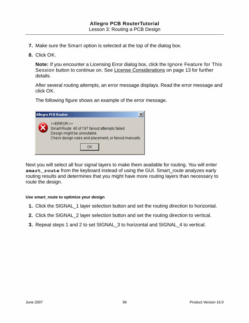
Allegro PCB RouterTutorialLesson 3: Routing a PCB Design
7. Make sure the Smart option is selected at the top of the dialog box.
8. Click OK.
Note: If you encounter a Licensing Error dialog box, click the Ignore Feature for ThisSession button to continue on. See License Considerations on page 13 for furtherdetails.
After several routing attempts, an error message displays. Read the error message andclick OK.
The following figure shows an example of the error message.
Next you will select all four signal layers to make them available for routing. You will entersmart_route from the keyboard instead of using the GUI. Smart_route analyzes earlyrouting results and determines that you might have more routing layers than necessary toroute the design.
Use smart_route to optimize your design
1. Click the SIGNAL_1 layer selection button and set the routing direction to horizontal.
2. Click the SIGNAL_2 layer selection button and set the routing direction to vertical.
3. Repeat steps 1 and 2 to set SIGNAL_3 to horizontal and SIGNAL_4 to vertical.
June 2007 96 Product Version 16.0

Allegro PCB RouterTutorialLesson 3: Routing a PCB Design
The Layer panel is shown in the following figure.
4. Close the Layer panel.
June 2007 97 Product Version 16.0

Allegro PCB RouterTutorialLesson 3: Routing a PCB Design
5. Enter smart_route in the command entry box below the routing status line and pressthe return key.
Note: If you encounter a Licensing Error dialog box, click the Ignore Feature for ThisSession button to continue on. See License Considerations on page 13 for furtherdetails.
After several routing passes, a message popup tells you that you might be able to reducethe number of layers. An example of the message popup is shown in the following figure.
6. Click OK to close the message popup.
7. Wait for Idle to replace the Pause button in the control area.
8. Enter quit in the command entry.
This command exits the autorouter without prompting you for a confirmation.
Understanding the Post-routing Commands
Post-routing commands refine the wiring and add test points after routing is complete. Theautorouter’s post-routing commands are spread, miter, testpoint, and recorner.The following table provides a brief description of the post-routing commands.
Table 3-1 Post Routing Commands
Command Description
spread Adds extra clearance between wires
testpoint Adds test points
miter Changes 90 degree corners to 45 degree diagonals using arange of setback values
recorner Changes 90 degree corners to 45 degree diagonals
June 2007 98 Product Version 16.0

Allegro PCB RouterTutorialLesson 3: Routing a PCB Design
All post-routing commands, except recorner, are DFM options. An explanation of the DFMpost-routing options is beyond the scope of this tutorial. See the Allegro PCB RouterCommand Reference for more information about using the spread, miter, andtestpoint commands.
When you use the recorner command, you must include a corner type and a setbackvalue. For example, the following command changes wrong way routes (slant) to 45 degreediagonals, if the slants are one inch or more in length.
recorner slant 1
The easiest way to change all 90 degree corners to 45 degree diagonals is to use recornerdiagonal with three setback values. An example of how you use this command is:
unit inchrecorner diagonal 1 1 1
In this example, the three setback values change 90 degree corners that meet the one inchcriteria to 45 degrees.
The recorner command is iterative. If at least one corner in the design changes to adiagonal, all remaining corners are attempted again. This iterative process continues until nofurther changes occur.
You achieve optimum results when you use a series of recorner commands withprogressively smaller setback values. In the following procedure, you enter two recornercommands and use setback values for the second that are half the value of the first.
Task: Change 90 degree corners to 45 degree diagonal corners
Procedure
1. Start PCB Router and load lesson3.dsn.
2. Choose File – Read – Routes.
The Read Routes dialog box opens.
3. Click the Browse button.
The Open dialog box opens for Windows platforms.
The Select File dialog box opens for UNIX platforms.
4. Change to the PCB Router tutorial directory for Windows platforms and openrecorner.rte.
June 2007 99 Product Version 16.0

Allegro PCB RouterTutorialLesson 3: Routing a PCB Design
Select recorner.rte and click OK for UNIX platforms.
The filename is added to the Read Routes dialog box.
5. Click OK.
The Routes file loads.
Note: If you have the DFM option, you can use a single miter command to replacesteps 6 through 8.
6. Enter recorner diagonal 1 1 1 in the command entry box.
Note: If you encounter a Licensing Error dialog box, click the Ignore Feature for ThisSession button to continue on. See License Considerations on page 13 for furtherdetails.
All 90 degree corners that meet the one inch setback criteria change to 45 degrees.
7. Wait for Idle to replace the Pause button in the control area.
8. Enter recorner diagonal 0.5 0.5 0.5.
9. Wait for Idle to replace the Pause button in the control area.
10. Examine the wiring changes made by the two previous recorner commands.
11. Enter quit in the command entry box to exit PCB Router.
With more complex designs, the following command series is suggested.
unit inchrecorner diagonal 1 1 1recorner diagonal 0.5 0.5 0.5recorner diagonal 0.25 0.25 0.25recorner diagonal 0.125 0.125 0.125
You can use other units and other values, but for best results always use a series ofrecorner commands. Start with a large setback value, and halve the previous value for thenext recorner command in the series.
Setting Routing Rules
PCB Router supports a large number of routing rules. Routing rules can be set at manydifferent levels. The routing rule levels are listed from highest to lowest precedence in thefollowing table.
June 2007 100 Product Version 16.0

Allegro PCB RouterTutorialLesson 3: Routing a PCB Design
Table 3-2 Routing Rule Levels
Rule level Description
region class to class Sets rules that apply between net classes when the nets arerouted in a region.
region net Sets rules that apply to nets in a region.
region class Sets rules that apply to a class of nets in a region.
region Sets rules for an area of the PCB.
padstack Sets clearance rules for via padstacks.
class to class layer Sets rules that apply between net classes when the nets arerouted on particular layers..
class to class Sets rules that apply between wires, pins, and vias of one ormore net classes.
fromto layer Sets rules that apply to connections if they are routed on aparticular layer.
fromto Sets rules for pin-to-pin connections.
group layer Sets rules that apply to a group of fromtos if the fromtos arerouted on a particular layer.
group Sets rules for a group of fromtos.
net layer Sets rules that apply to nets if they are routed on a particularlayer.
net Sets rules that apply to nets.
group set layer Sets rules that apply to a set of groups when they are routedon a particular layer.
group set Sets rules that apply to a set of groups.
class layer Sets rules that apply to a class of nets if the nets are routedon a particular layer.
class Sets rules that apply to a class of nets.
layer Sets rules that apply to wires routed on a particular layer.
pcb Sets global rules for all nets in the design. This is the lowestprecedence rule.
June 2007 101 Product Version 16.0
Allegro PCB RouterTutorialLesson 3: Routing a PCB Design
Understanding PCB Router’s rule hierarchy
The rule levels described in the previous table form a hierarchy. Higher level rules alwaysoverride lower level rules that are set for the same physical objects. For example, a wire-to-wire clearance rule for a net overrides a wire-to-wire clearance rule for a class that includesthat net.
Rules at the PCB level have the lowest precedence in the hierarchy. Rules at the region classto class level have the highest precedence in the hierarchy. The order of precedence is fixedand cannot be changed.
Setting Width and Clearance Rules
You can set width and clearance rules at different levels of the hierarchy and for differentobjects. The object types supported by the autorouter are described in the following table.
Table 3-3 Object Types
Two object types separated by the underscore character indicate an object-to-object rule. Forexample, wire_smd is used to set clearance rules between wires and SMD pads.
Task: Set width and clearance rules at the PCB level
Procedure
1. Start PCB Router and load lesson3.dsn.
2. Choose Rules – PCB – Clearance.
The PCB Clearance Rules dialog box opens, as shown in the following figure.
3. Enter 0.007 in the Wire Width data entry box.
Object type What it means
area Keepout regions and PCB boundary
pad SMD pad
pin Through-pin
via Layer feed-through
wire Copper path
June 2007 102 Product Version 16.0

Allegro PCB RouterTutorialLesson 3: Routing a PCB Design
4. Enter 0.007 for wire_wire clearance.
This data entry box is located in the row labeled Wire under the column labeled Wire.
5. Click OK.
The width and clearance rules that you changed in the PCB Clearance Rules dialog boxare applied.
6. View the session transcript in the Output window and find the following commands:
rule pcb (clearance 0.007 (type wire_wire))rule pcb (width 0.007)
7. Enter quit in the Command entry box to exit PCB Router.
In Lesson 4, you will learn to set additional routing rules.
June 2007 103 Product Version 16.0

Allegro PCB RouterTutorialLesson 3: Routing a PCB Design
Autorouting With a Do File
There are three methods for issuing commands and controlling the autorouter.You can:
■ use the GUI.
■ enter commands from the keyboard.
■ use a Do file.
Until now, you either used the GUI to run commands or you entered console commands usingthe keyboard. The preferred method for controlling the autorouter is with a Do file. A Do fileis a text file that contains one or more autorouting commands. Each command occupies aseparate line in the Do file. Commands are organized in the order you want them to run fromthe start to the end of the file.
The Do file also serves another purpose. It serves as a record of the rules and commandsyou use during an autorouting session. If you need to apply a design revision to a completeddesign, you can edit the original Do file and reuse it.
You start with a basic Do file that includes commands that address the following:
■ Setup and file management
■ Rule setting
■ Prerouting
■ Routing
■ Post-routing
Using a basic Do file
A basic Do file (basic.do) is included with the tutorial files. A listing of the commands inbasic.do follows. The PCB width and clearance rules are not intended as typical valuesbut are included as examples.
bestsave on $\best.wirstatus_file $\route.stsunit milrule pcb (clearance 7 (type wire_wire))rule pcb (width 7)smart_route
June 2007 104 Product Version 16.0

Allegro PCB RouterTutorialLesson 3: Routing a PCB Design
write routes $\final.rtereport status $\final.sts
Note: The $\ notation represents the path for the file in PCB Router. When you want to writea report or data file to the same directory where the design file is located, use the $\ notation.On UNIX platforms, substitute the / character for the \ character.
Often, you do not need to include PCB clearance and width rules in the Do file, because theyare translated from your layout system and embedded in the Design file. If you want tooverride rules that were set in the layout system or you want to apply other rules, add yourrules to the Do file. Make sure these rules precede all routing commands.
Task: Use a basic do file to autoroute a PCB design
Click on the following link to see how this is done before attempting the task on your own.
Show me
This demonstration runs in your browser for approximately 4 minutes and 28 seconds.
Procedure
1. Start PCB Router and enter the path for lesson3.dsn in the Design/Session File dataentry box.
2. Enter $\basic.do in the Do File data entry box located on the dialog box. On a UNIXplatform, substitute / for \.
3. Click Start Allegro PCB Router.
Once you have selected a product, PCB Router starts, loads the Design file, and runsthe Do file.
Note: If you encounter a Licensing Error dialog box, click the Ignore Feature for ThisSession button to continue on. See License Considerations on page 13 for furtherdetails.
A Pause button appears in the control area.
Note: After several routing passes, one or more message popups may appear.Click OK to dismiss these message popups.
4. Wait for Idle to replace the Pause button in the control area.
5. View the session transcript in the Output window, and verify that all commands were run.
Note: If a Do file contains a syntax error, the Do file stops working and the error is
June 2007 105 Product Version 16.0
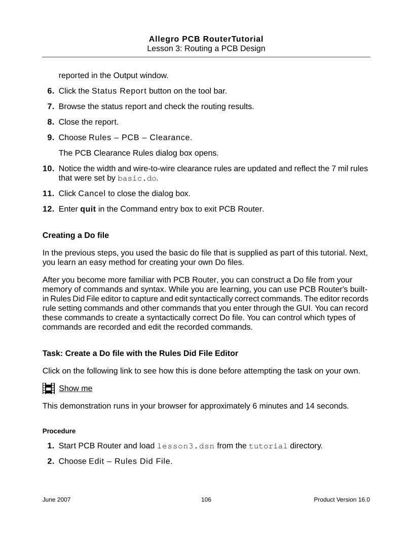
Allegro PCB RouterTutorialLesson 3: Routing a PCB Design
reported in the Output window.
6. Click the Status Report button on the tool bar.
7. Browse the status report and check the routing results.
8. Close the report.
9. Choose Rules – PCB – Clearance.
The PCB Clearance Rules dialog box opens.
10. Notice the width and wire-to-wire clearance rules are updated and reflect the 7 mil rulesthat were set by basic.do.
11. Click Cancel to close the dialog box.
12. Enter quit in the Command entry box to exit PCB Router.
Creating a Do file
In the previous steps, you used the basic do file that is supplied as part of this tutorial. Next,you learn an easy method for creating your own Do files.
After you become more familiar with PCB Router, you can construct a Do file from yourmemory of commands and syntax. While you are learning, you can use PCB Router’s built-in Rules Did File editor to capture and edit syntactically correct commands. The editor recordsrule setting commands and other commands that you enter through the GUI. You can recordthese commands to create a syntactically correct Do file. You can control which types ofcommands are recorded and edit the recorded commands.
Task: Create a Do file with the Rules Did File Editor
Click on the following link to see how this is done before attempting the task on your own.
Show me
This demonstration runs in your browser for approximately 6 minutes and 14 seconds.
Procedure
1. Start PCB Router and load lesson3.dsn from the tutorial directory.
2. Choose Edit – Rules Did File.
June 2007 106 Product Version 16.0
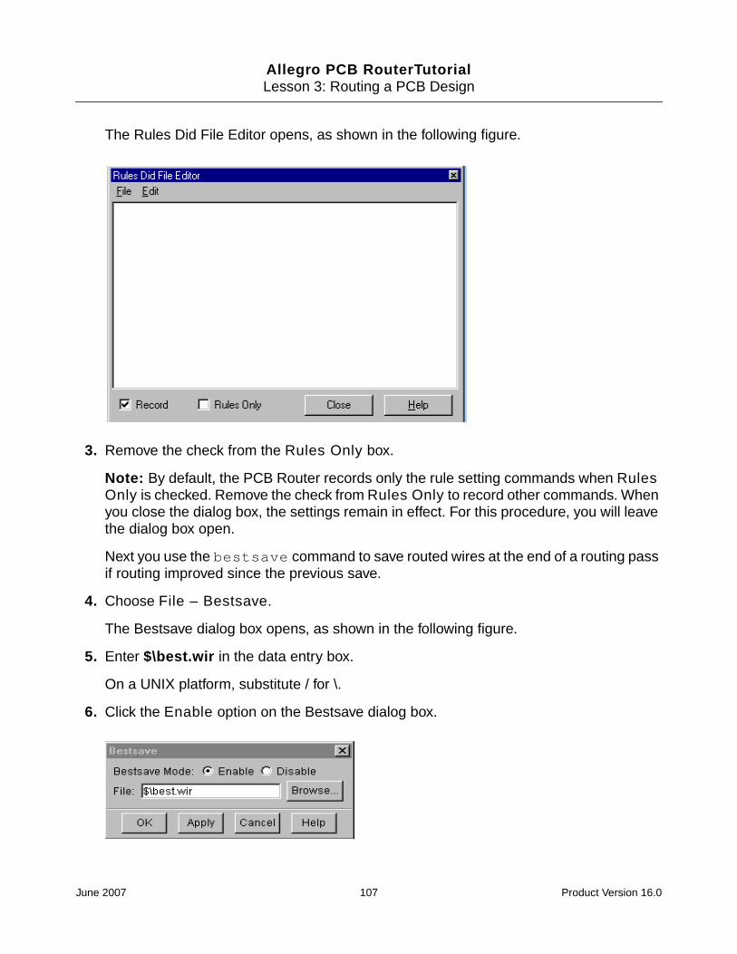
Allegro PCB RouterTutorialLesson 3: Routing a PCB Design
The Rules Did File Editor opens, as shown in the following figure.
3. Remove the check from the Rules Only box.
Note: By default, the PCB Router records only the rule setting commands when RulesOnly is checked. Remove the check from Rules Only to record other commands. Whenyou close the dialog box, the settings remain in effect. For this procedure, you will leavethe dialog box open.
Next you use the bestsave command to save routed wires at the end of a routing passif routing improved since the previous save.
4. Choose File – Bestsave.
The Bestsave dialog box opens, as shown in the following figure.
5. Enter $\best.wir in the data entry box.
On a UNIX platform, substitute / for \.
6. Click the Enable option on the Bestsave dialog box.
June 2007 107 Product Version 16.0

Allegro PCB RouterTutorialLesson 3: Routing a PCB Design
7. Click OK.
Notice that the command is recorded in the Rules Did File Editor.
Next you will change the measurement unit to mils.
8. Click the Unit button (near the bottom right corner of the window) and choose mil.
9. Choose Rules – PCB – Clearance.
The PCB Clearance Rules dialog box opens, as shown in the following figure.
10. Enter 7 in the Wire Width data entry box.
11. Enter 7 in the wire_wire clearance data entry box.
The wire_wire clearance data entry box is in the row labeled Wire, under the columnlabeled Wire.
12. Click OK.
13. Choose Autoroute – Route.
June 2007 108 Product Version 16.0
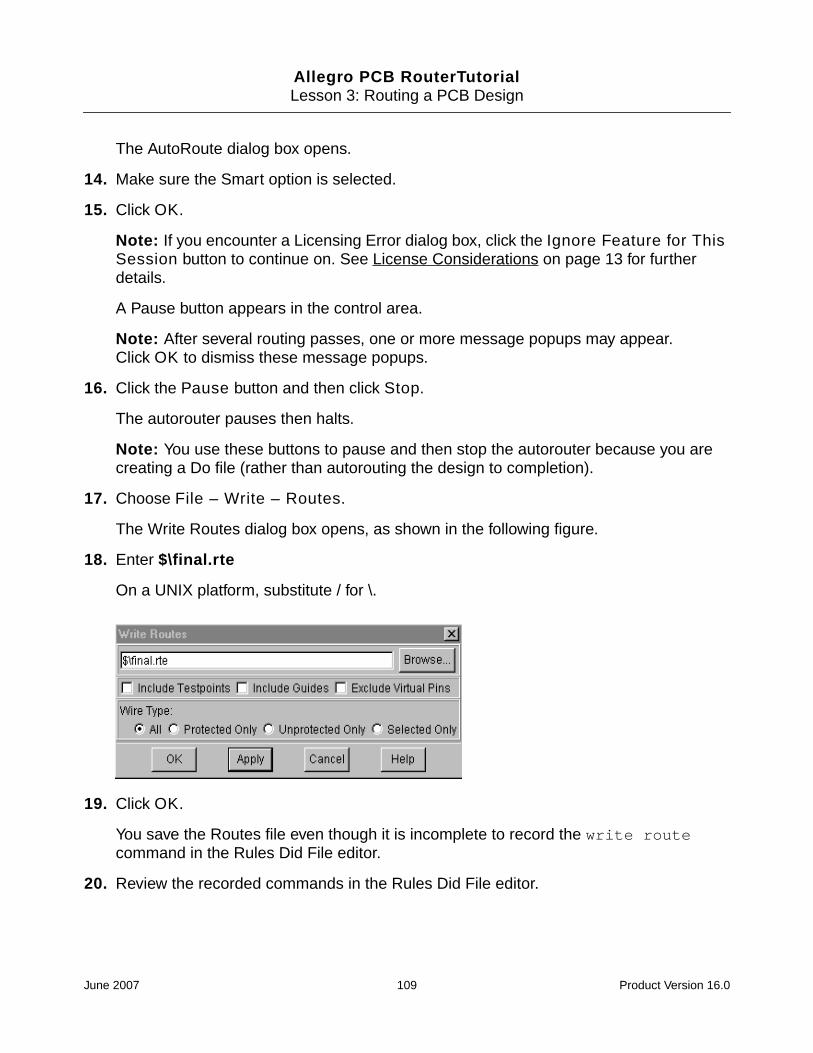
Allegro PCB RouterTutorialLesson 3: Routing a PCB Design
The AutoRoute dialog box opens.
14. Make sure the Smart option is selected.
15. Click OK.
Note: If you encounter a Licensing Error dialog box, click the Ignore Feature for ThisSession button to continue on. See License Considerations on page 13 for furtherdetails.
A Pause button appears in the control area.
Note: After several routing passes, one or more message popups may appear.Click OK to dismiss these message popups.
16. Click the Pause button and then click Stop.
The autorouter pauses then halts.
Note: You use these buttons to pause and then stop the autorouter because you arecreating a Do file (rather than autorouting the design to completion).
17. Choose File – Write – Routes.
The Write Routes dialog box opens, as shown in the following figure.
18. Enter $\final.rte
On a UNIX platform, substitute / for \.
19. Click OK.
You save the Routes file even though it is incomplete to record the write routecommand in the Rules Did File editor.
20. Review the recorded commands in the Rules Did File editor.
June 2007 109 Product Version 16.0

Allegro PCB RouterTutorialLesson 3: Routing a PCB Design
Edit the Do file with the Rules Did File Editor
In the previous procedure, you used the Rules Did File editor to record commands that youentered through the GUI. You can record all commands this way. In the following procedure,you will enhance this Do file by entering additional commands and comments into the editorwindow.
Note: A pound sign (#) precedes a comment. PCB Router ignores comments in do files.
Task: Edit the Do file by adding commands and comments
Procedure
1. Add the following commands and comments to the Rules Did File editor. On UNIXplatforms, substitute the / character for the \ character.
2. Save the file in the tutorial directory as mybasic.do.
3. Close the Rules Did File editor.
4. Enter quit in the Command entry box to exit PCB Router.
June 2007 110 Product Version 16.0

Allegro PCB RouterTutorialLesson 3: Routing a PCB Design
Monitoring Autorouting Progress
In Lesson 1 you learned about the status report and about the kinds of information it contains.Now you will learn how to use the status report to monitor autorouting progress anddetermine when and how to adjust your strategy.
The smart_route command uses the same information that is recorded in the status reportto analyze autorouting progress. Progress is gauged by monitoring failures, unroutes, andconflict reduction from pass to pass. These terms are explained in the following table.
Table 3-4 Routing Terminology
Using the status report
The Routing History table is updated in the status report for each routing pass. This tablecontains the information you need to analyze routing progress.
When you use smart_route, it analyzes the status information for you and alerts you whenpotential problems are detected or when a design reduction might be possible. If you usebasic autorouting commands instead of smart_route, you must monitor and analyze thestatus report to determine whether adjustments are needed. To gauge whether the autorouteris making good progress and determine what must be done if progress is poor, you need tounderstand the indicators of both good and poor routing progress.
Term What it means
conflict Conflicts consist of two types.Crossing conflicts occur when two wires cross.Clearance conflicts occur when a wire or viaviolates a clearance rule.
failure A failure occurs when the autorouter attempts toroute or reroute a connection, fails, and restoresthe connection to its prior state.
reduction % Reduction % indicates the percentage of conflictreduction compared to the previous pass.
unroute An unroute is a connection that is not routed.
June 2007 111 Product Version 16.0

Allegro PCB RouterTutorialLesson 3: Routing a PCB Design
Analyzing Conflicts
The number of conflicts after the first route pass is a good indication of whether a design canbe routed completely. When the sum of crossing and clearance conflicts is less than five timesthe total number of connections, routing is likely to complete. The following figure shows astatus file with a good ratio between total conflicts and total connections after the first routepass.
Figure 3-4 Status File with a Good Conflict/Connection Ratio
Indicators show that the design is routable.
If the total number of conflicts after the first pass is more than five times the total number ofconnections, this usually indicates the design will not route because of one or more of thereasons listed in the following table.
June 2007 112 Product Version 16.0

Allegro PCB RouterTutorialLesson 3: Routing a PCB Design
Table 3-5 Unroutable Design Problems
Task: Use the status report to determine a design problem
Procedure
1. Start PCB Router and load conflict.dsn.
If a warning dialog box appears, close it.
Cause Meaning Solution
Insufficient routing layers Layers are unselected or toofew signal layers are defined inthe layout system.
Use the Layers panel todetermine whether signallayers are unselected.
Layer routing directions areincorrect
An insufficient number ofvertical or horizontal routinglayers are defined. Theautorouter eventually resolvesthis, but it takes longer to routethe design.
Use the Layers panel todetermine whether signallayer directions are setcorrectly.
Power and ground nets arebeing routed
Power and ground nets are notdefined as copper planes, andthe autorouter is routing powerand ground connections.
Use the Layers panel todetermine whether powerlayers are defined correctly.If power layers are definedcorrectly, you cannot selector unselect the layers andcannot set the routingdirection in the Layers panel.If power layers are notdefined correctly, fix theproblem in the layout systemand re-extract the design.
Clearance rules areincorrect
An error was made in settingclearance rule values.
Make sure that the rulevalues are set correctly forthe current unit setting.
Prerouted wires areprotected
Protected preroutes prevent theautorouter from ripping up andrerouting connections toeliminate conflicts.
Try autorouting with thepreroutes unprotected.
June 2007 113 Product Version 16.0
Allegro PCB RouterTutorialLesson 3: Routing a PCB Design
2. Enter route 1 in the command entry box.
Note: If you encounter a Licensing Error dialog box, click the Ignore Feature for ThisSession button to continue on. See License Considerations on page 13 for furtherdetails.
The Pause button appears in the status bar.
Wait for Idle to replace the Pause button in the control area.
3. Click the Status Report button on the tool bar.
4. Observe the number of crossing and clearance conflicts and the failures in the RoutingHistory table.
The number of failures indicates a design problem, which in this case are the result oftoo few routing layers.
5. Enter quit in the command entry box to exit PCB Router.
Analyzing Failures
A failure occurs when the autorouter cannot route or reroute a connection. Routing failuresare the same as unroutes during the first route pass and can indicate a difficult design, adesign error, or unrealistic design rules.
There are usually no failures during the first route pass, because the cost for allowing conflictsis lower during the first pass than at any other time. If a small percentage of the totalconnections (less than 2%) fail during the first pass, this could indicate a difficult design. Ifmore than 2% of the total connections fail during the first pass (and the total number ofconflicts is high), the cause is usually a design problem.
Failures that occur during and after the second route pass indicate the number of connectionsthat could not be routed with a different path and were restored to their previous state. Failedconnections after the first route pass are not necessarily a problem, unless they accompanyexcessive conflicts or unroutes.
Analyzing Conflict Reduction
After the first route pass and through pass five, the total number of conflicts should reduce byat least 30% per pass. If conflict reduction is less than 30% per pass during this phase, therecan be several causes as listed in the following table.
June 2007 114 Product Version 16.0
Allegro PCB RouterTutorialLesson 3: Routing a PCB Design
Table 3-6 Conflict Reduction Problems
After pass five, conflict reduction proceeds at a slower pace. Although the percentage ofreduction is usually much less for each pass of this phase, conflicts should always follow adownward trend over a series of ten passes.
Analyzing Unroutes
Unroutes should not exist after the fifth routing pass. If unroutes remain after the fifth routepass, the unroutes will probably remain at the conclusion of the autorouting session. Thetypical causes for unroutes after route pass five are explained in the following table.
Table 3-7 Unroutes Problems
Cause Meaning Solution
Difficult design The design is very dense, anda larger than usual number ofrouting passes is required toroute to 100%.
Increase the total number ofrouting passes. Using severalhundred routing passes withdifficult designs is not unusual.
Insufficient routing layers An insufficient number ofsignal layers is defined orlayers are unselected.
Use the Layers panel todetermine whether signallayers are unselected.
Autorouter is via starved The via grid is too coarse,which prevents the autorouterfrom eliminating conflicts byadding vias.
Set the via grid to zero or to aminimum resolution.
For example, the followingcommands set both wire andvia grids to 1 mil.
unit milgrid smart(via1)(wire 1)
Cause Meaning Solution
Keepouts block pins Pins covered by keepouts cannotbe routed.
Check the unroutedconnections to determinewhether they are blocked orcovered by keepouts.
June 2007 115 Product Version 16.0
Allegro PCB RouterTutorialLesson 3: Routing a PCB Design
In this section, you learned how to detect autorouting problems and what you can do aboutthem. Use this information, to solve routing problems when you are routing your designs.
What You Learned
In this lesson, you learned how to automatically route a PCB design. You learned how theautorouter works and how to:
■ set routing rules.
■ use a Do file.
■ monitor autorouting progress.
In the next lesson, you will learn how to set rules and control the autorouter.
Component pins overlap If components are placedincorrectly and pins overlap, thepins cannot be routed.
Make sure the pins do notoverlap.
Pins are outside the PCBboundary
Pins that are outside or too nearthe PCB boundary cannot berouted.
Check the unroutedconnections to determinewhether they are eitheroutside or too near the PCBboundary.
Cause Meaning Solution
June 2007 116 Product Version 16.0
Allegro PCB RouterTutorial
4Lesson 4: Setting Rules and Constraints
What You Will Learn
This lesson teaches you how to set wiring rules and use commands that control the way adesign is routed. This lesson differs from the previous lessons because you enter mostcommands from the keyboard instead of using the GUI.
In this lesson you will learn how to:
■ set rules at different levels in the rules hierarchy.
■ set wire and via clearance rules for different objects.
■ select layers for routing.
■ set layer routing direction.
■ select vias for routing.
■ select connections for routing.
■ use routing keepins.
■ control whether nets are routed with starburst or daisy-chain wiring.
■ define a class of nets and a group of fromtos.
■ assign rules to classes and groups.
■ assign routing priorities.
This lesson takes about 60 minutes to complete.
What to do Before You Begin
Before you begin this lesson, do the following:
■ Complete Lesson 3: Routing a PCB Design.
June 2007 117 Product Version 16.0

Allegro PCB RouterTutorialLesson 4: Setting Rules and Constraints
Understanding the Autorouter’s Hierarchical Rules
In Lesson 3, you learned that you can set rules at 19 different levels to control how a designis routed. The following figure shows the 19 rule levels.
June 2007 118 Product Version 16.0

Allegro PCB RouterTutorialLesson 4: Setting Rules and Constraints
Rules set at higher levels override those set at lower levels, when they apply to the sameobject. For example, if you set the following rules:
unit mil
rule pcb (clearance 8 (type wire_wire))
rule net (CLK (clearance 10 (type wire_wire))
all nets obey the pcb 8 mil wire-to-wire clearance rule, except net CLK, which obeys the 10mil clearance rule. Because both rules control wire-to-wire clearance, the higher precedencenet rule overrides the pcb rule for the net CLK.
If you set the following rules:
unit mil
rule pcb (clearance 8 (type wire_smd))
rule net CLK (clearance 10 (type wire_pin))
the CLK net obeys both the 8 mil wire-to-smd PCB clearance rule and the 10 mil wire-to-pinnet clearance rule. Both rules are followed, because they are set for different objects and theydo not conflict.
In the following procedure, you set wire width rules at the pcb, net, and fromto levels.
Task: Set wire width rules at the pcb, net, and fromto levels
Procedure
1. Start PCB Router and load lesson4.dsn from the tutorial directory. See Where tofind the Accompanying Lesson Files on page 12 for the location of this directory.
2. Type rule pcb (width .008) in the command entry box.
3. Type rule net sig1 (width .012).
4. Type define (net sig1 (fromto U7-1 U8-1 (rule (width .020)))).
5. Type select net sig1 sig2 sig3 sig4.
6. Type bus diagonal.
7. Type unselect all nets.
8. Examine the wiring that was routed using bus diagonal.
June 2007 119 Product Version 16.0
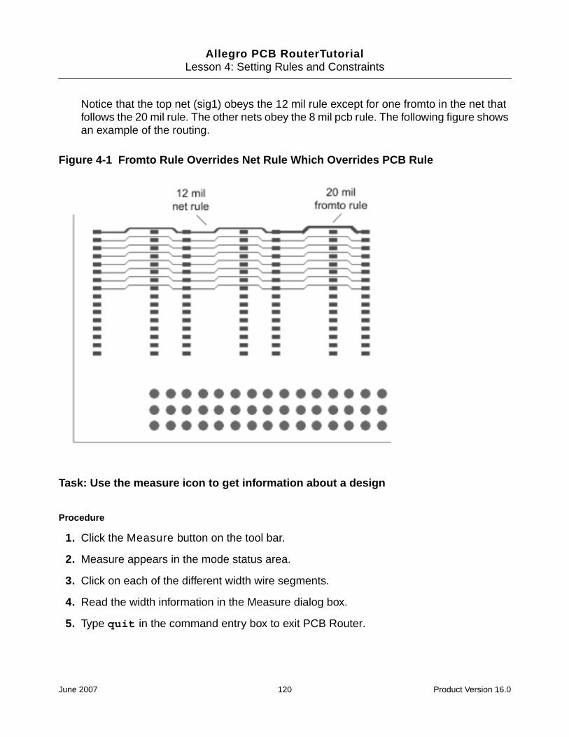
Allegro PCB RouterTutorialLesson 4: Setting Rules and Constraints
Notice that the top net (sig1) obeys the 12 mil rule except for one fromto in the net thatfollows the 20 mil rule. The other nets obey the 8 mil pcb rule. The following figure showsan example of the routing.
Figure 4-1 Fromto Rule Overrides Net Rule Which Overrides PCB Rule
Task: Use the measure icon to get information about a design
Procedure
1. Click the Measure button on the tool bar.
2. Measure appears in the mode status area.
3. Click on each of the different width wire segments.
4. Read the width information in the Measure dialog box.
5. Type quit in the command entry box to exit PCB Router.
June 2007 120 Product Version 16.0
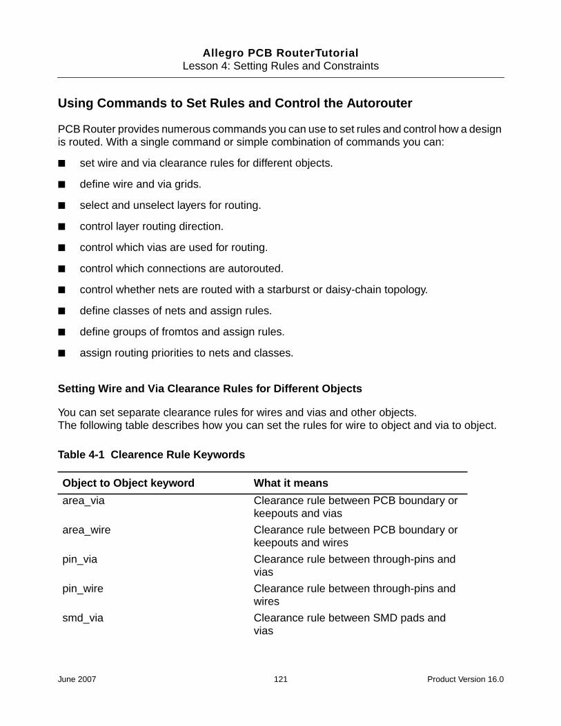
Allegro PCB RouterTutorialLesson 4: Setting Rules and Constraints
Using Commands to Set Rules and Control the Autorouter
PCB Router provides numerous commands you can use to set rules and control how a designis routed. With a single command or simple combination of commands you can:
■ set wire and via clearance rules for different objects.
■ define wire and via grids.
■ select and unselect layers for routing.
■ control layer routing direction.
■ control which vias are used for routing.
■ control which connections are autorouted.
■ control whether nets are routed with a starburst or daisy-chain topology.
■ define classes of nets and assign rules.
■ define groups of fromtos and assign rules.
■ assign routing priorities to nets and classes.
Setting Wire and Via Clearance Rules for Different Objects
You can set separate clearance rules for wires and vias and other objects.The following table describes how you can set the rules for wire to object and via to object.
Table 4-1 Clearence Rule Keywords
Object to Object keyword What it means
area_via Clearance rule between PCB boundary orkeepouts and vias
area_wire Clearance rule between PCB boundary orkeepouts and wires
pin_via Clearance rule between through-pins andvias
pin_wire Clearance rule between through-pins andwires
smd_via Clearance rule between SMD pads andvias
June 2007 121 Product Version 16.0
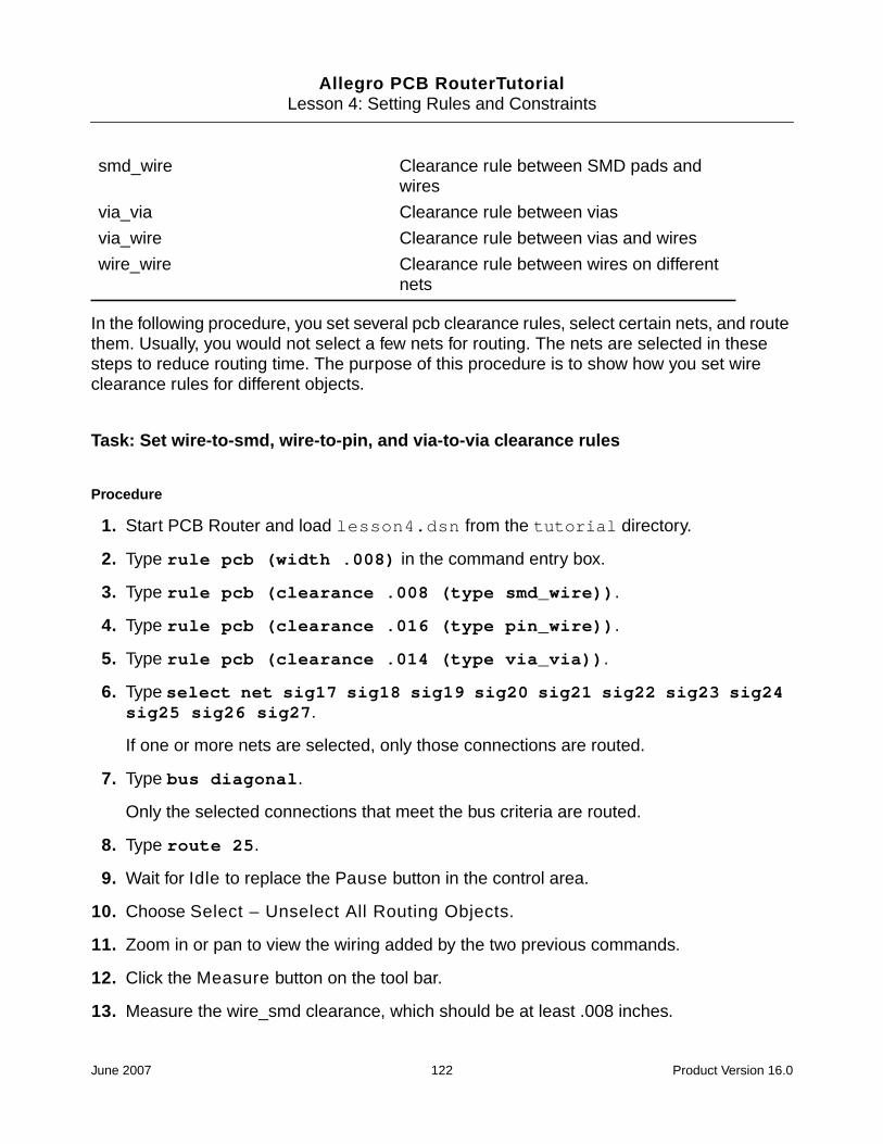
Allegro PCB RouterTutorialLesson 4: Setting Rules and Constraints
In the following procedure, you set several pcb clearance rules, select certain nets, and routethem. Usually, you would not select a few nets for routing. The nets are selected in thesesteps to reduce routing time. The purpose of this procedure is to show how you set wireclearance rules for different objects.
Task: Set wire-to-smd, wire-to-pin, and via-to-via clearance rules
Procedure
1. Start PCB Router and load lesson4.dsn from the tutorial directory.
2. Type rule pcb (width .008) in the command entry box.
3. Type rule pcb (clearance .008 (type smd_wire)).
4. Type rule pcb (clearance .016 (type pin_wire)).
5. Type rule pcb (clearance .014 (type via_via)).
6. Type select net sig17 sig18 sig19 sig20 sig21 sig22 sig23 sig24sig25 sig26 sig27.
If one or more nets are selected, only those connections are routed.
7. Type bus diagonal.
Only the selected connections that meet the bus criteria are routed.
8. Type route 25.
9. Wait for Idle to replace the Pause button in the control area.
10. Choose Select – Unselect All Routing Objects.
11. Zoom in or pan to view the wiring added by the two previous commands.
12. Click the Measure button on the tool bar.
13. Measure the wire_smd clearance, which should be at least .008 inches.
smd_wire Clearance rule between SMD pads andwires
via_via Clearance rule between vias
via_wire Clearance rule between vias and wires
wire_wire Clearance rule between wires on differentnets
June 2007 122 Product Version 16.0
Allegro PCB RouterTutorialLesson 4: Setting Rules and Constraints
14. Measure the wire_pin clearance.
Notice the 0.016 wire-to-pin clearance rule centers wires between through-pins.
15. Measure the via_via clearance.
Vias obey the 0.014 (minimum) via-to-via clearance rule.
16. Type quit in the command entry box to exit PCB Router.
Selecting Layers for Routing
When a signal layer is selected, it is available for routing. If a signal layer is unselected, it isnot used for routing unless it is an external layer on which SMD components are mounted orcertain nets are assigned to route on that layer. You can assign a net to route on a particularlayer (if you have the ADV option) by using the circuit command with a use_layer rule.
The commands that enable or disable a signal layer for routing are select layer andunselect layer. When you use these commands, include the name of the layer you wantto control.
For example:
select layer TOP
unselect layer INT1
Setting Layer Routing Directions
If layer routing directions are not set in the layout system, PCB Router sets each signal layer’srouting direction to horizontal or vertical. The top signal layer is set to horizontal, and the nextsignal layer below the top layer uses a vertical direction. The autorouter alternates betweenhorizontal and vertical directions for each additional signal layer.
You can override the default layer routing directions by using the Layers panel or by using thedirection command. If the interconnection between components is biased more in ahorizontal or vertical direction, change the routing direction of some signal layers toaccommodate the bias. Include the layer name and the horizontal or vertical keyword withthe direction command to control layer routing direction.
For example:
direction SIGNAL_2 vertical
June 2007 123 Product Version 16.0

Allegro PCB RouterTutorialLesson 4: Setting Rules and Constraints
Select layers for routing and set layer routing direction
1. Start the autorouter and load lesson4.dsn.
2. Click the Layers button on the tool bar.
The Layers panel opens. The default signal layers directions display as follows:
3. Type unselect layer SIGNAL_2 in the command entry box.
The button in the Layers panel for SIGNAL_2 changes to
4. Type direction SIGNAL_1 vertical in the command entry box.
5. Notice the button in the Layers panel for SIGNAL_1 changes to
Use the direction command to change the routing direction for the other signallayers.
6. Type direction SIGNAL_2 horizontal in the command entry box.
Notice in the Layers panel that the direction command changes the layer’s routingdirection and selects the layer.
7. Type quit in the command entry box and exit the autorouter.
Selecting Vias for Routing
The vias you can use in the autorouter are the vias included by your layout system. Usually,all vias in a design are selected and available for routing, but you can unselect vias that youdo not want to use.
The select and unselect commands control which vias are available for routing. Viasthat are defined in the design but are unselected, are not available for routing.
SIGNAL_1SIGNAL_2SIGNAL_3SIGNAL_4
June 2007 124 Product Version 16.0
Allegro PCB RouterTutorialLesson 4: Setting Rules and Constraints
When two or more vias are available for a transition between two layers, the autorouterchooses the one that uses the fewest layers and has the smallest shapes. You can use blindand buried vias if you have the HYB option.
Note: You can assign specific vias to nets, classes, and groups of fromtos if you have theADV option.
Task: Select a single via for routing
Procedure
1. Start PCB Router and load lesson4.dsn from the tutorial directory.
2. Choose Report – Specify.
The Report specify opens.
3. Click on Vias.
The Via Report opens.
4. Browse the report and observe that all vias are selected for routing.
5. Close the report when you finish browsing.
6. Type unselect all vias in the command entry box.
7. Type select via VIA35.
8. Repeat steps 2 and 3.
9. The report indicates that all vias are unselected for routing except VIA35.
10. Close the report when you finish browsing.
11. Type quit in the command entry box to exit PCB Router.
Selecting Connections and Autorouting
If one or more connections are selected, only those connections are routed. Usually you donot route fewer than all connections. You can assign connections a priority if you want tocontrol when certain nets are routed. See Assigning Routing Priorities to Nets andClasses later in this lesson.
Occasionally you might want to route fewer than all connections in order to check rule settingsor to experiment. You can choose the connections you want to route by selecting them.
June 2007 125 Product Version 16.0

Allegro PCB RouterTutorialLesson 4: Setting Rules and Constraints
You can select connections by component, net, class group and fromto.
The following table describes the commands that implement the selection methods.
Table 4-2 Commands that Select
PCB Router highlights selected connections in the “select color,” which is usually yellow.
After you select connections, you can apply rules and controls to the connections, then routethe connections. Usually, you unselect connections after they are routed.
Use the unselect command to return components, nets, classes, groups, and fromtos tonormal status. The unselect all routing command is used when you want to makecertain that all previously selected routing objects are unselected, and that all unroutedconnections can be routed.
Task: Autoroute selected connections
Click on the following link to see how this is done before attempting the task on your own.
Show me
This demonstration runs in your browser for approximately 3 minutes and 0 seconds.
Procedure
1. Start PCB Router and load lesson4.dsn from the tutorial directory.
2. Click the Select Component button on the tool bar.
Command What it does
select component <id> Selects the connections that are attached tothe component identified by <id>, which isthe component’s reference designator.
select net <id> Selects all connections on the net identifiedby <id>.
select class <id> Selects all the nets that are members of theclass identified by <id>.
select group <id> Selects all the fromtos (connections) that aremembers of the group identified by <id>.
select fromto Selects all unrouted connections.
June 2007 126 Product Version 16.0

Allegro PCB RouterTutorialLesson 4: Setting Rules and Constraints
Sel Comp appears in the mode status area.
3. Click on a pin or inside the outline of any component.
All pins on the component and all attached connections are selected.
4. Click on any pin of the same component.
The component is unselected.
5. Click the Select Net button on the tool bar.
6. Click on any pin that has a guide attached.
All connections on the net are selected.
7. Drag the pointer across several pins.
The nets attached to the pins are selected.
8. Click the Select Guide button on the tool bar.
9. Drag the pointer across several guides.
The connections attached to the guides are selected.
10. Type unselect all routing in the command entry box.
All connections are unselected.
11. Type select net sig1 sig2.
12. Type bus diagonal.
13. Type select component U1.
14. Type route 25.
Although this command specifies 25 route passes, only two are needed to route theselected connections. The remaining passes are skipped.
15. Type unselect all routing.
June 2007 127 Product Version 16.0

Allegro PCB RouterTutorialLesson 4: Setting Rules and Constraints
Using Routing Keepin Regions
Another method you can use to limit autorouting to fewer than all connections is to create oneor more fences. A fence is a keepin boundary for the connections it encloses.
Connections that span a fence’s boundaries or that lie completely outside the boundaries, areignored during routing. You can define one or more individual fences to restrict the routing inseveral areas. If you create fences that overlap, they merge to form a single, polygonal fenceregion.
You create fences using one of the following methods.
■ Draw a fence.
■ Use a dialog box to enter the fence coordinates.
■ Use the fence command.
The easiest method for creating a fence is to draw it, but often you need to create the fencein your Do file. In a Do file, you use the fence command. Before you write the Do file, usethe mouse to draw the fence, determine the coordinates from the Did file, and then use thecoordinates in your Do file.
Task: Draw a fence and only route the enclosed connections
Click on the following link to see how this is done before attempting the task on your own.
Show me
This demonstration runs in your browser for approximately 3 minutes and 27 seconds.
Procedure
1. Type delete all wires in the command entry box.
A message popup prompts you to confirm the command. (The autorouter should berunning with lesson4.dsn loaded.)
2. Click Yes to delete all wires.
You need to display component reference designators.
3. Choose View – Labels.
The View Labels dialog box opens.
June 2007 128 Product Version 16.0

Allegro PCB RouterTutorialLesson 4: Setting Rules and Constraints
Make sure Ref Des is selected.
4. Click OK.
The component reference designators display.
5. Choose Define – Fence – Draw Mode.
Draw Fence appears in the mode status area.
6. Drag the pointer and draw a fence around components U5, U6, U7, and U8, as shown inthe following figure. If you do not like the fence you drew, choose Define – Fence –Draw Mode to remove the fence and start with step 6 to draw a new fence.
7. Press the right mouse button and choose Define Polygon As Fence from the menu.
8. View the session transcript in the Output window, and locate the mode edit fence,area init_pt, and area add_pt commands.
June 2007 129 Product Version 16.0
Allegro PCB RouterTutorialLesson 4: Setting Rules and Constraints
The X,Y coordinates beside the area_init_pt and area_add_pt commandsrepresent diagonally opposite corners of the fence.
9. Read the coordinate information beside the area init_pt and area add_ptcommands.
You could use this coordinate information with the fence command in a Do file.
For example,
fence 0.6 6.85 2.75 7.75.
10. Type bus diagonal in the command entry box.
11. Type route 25.
The autorouter routes only the connections that are completely inside the fence region.
12. Wait for Idle to replace the Pause button in the control area and type quit in thecommand entry box to exit PCB Router.
Note: You can also use soft fences if you have the FST option. Soft fences are useful formaintaining separation between analog and digital circuits. See the set command in theAllegro PCB Router Command Reference for additional information about soft fences.
Controlling Whether Nets are Routed With Starburst or Daisy-ChainWiring
Nets are usually ordered for starburst routing because it produces the most efficient wiring.Ordering determines how the pins on a net are wired. Starburst is the most efficient becausethe autorouter orders and routes starburst nets with minimum wire lengths. The followingfigure shows the basic difference between starburst and daisy-chain wiring.
June 2007 130 Product Version 16.0

Allegro PCB RouterTutorialLesson 4: Setting Rules and Constraints
Figure 4-2 Comparison Between Starburst and Daisy-Chain Wiring
Nets are ordered for daisy-chain routing in the layout system and translated to the Design file,or they can be ordered in PCB Router. All nets default to starburst ordering unless they areexplicitly ordered as daisy-chain.
Use the order command to define net ordering. For example, order daisy net <netid> orders a single net for daisy-chain routing. Replace <net id> in the command with thename of the net you want to order.
When you order a net for daisy-chain routing, you often want to control which pins are source,load, and terminator. If you do not assign these properties, PCB Router treats all pins on adaisy-chain net as loads and chains them together in an optimum configuration.
You use the assign_pin command to assign source, load, or terminator properties to pins.If a net has only one pin on a given component, you can assign a property to that pin byreferencing the component and then ordering the net.
For example:
assign_pin source U23
assign_pin terminator U29
order daisy net SO1
If a net has several pins on a single component, you assign pin properties by adding the pinIDs to the command.
For example:
assign_pin source U33 (pins 2)
assign_pin terminator U33 (pins 11)
June 2007 131 Product Version 16.0

Allegro PCB RouterTutorialLesson 4: Setting Rules and Constraints
order daisy net PRX
Note: You assign source, load, or terminator properties to pins before you use the ordercommand. If you assign pin properties but do not use the order command, the propertiesare ignored by the autorouter.
Task: Assign pin properties and order a net for daisy-chain routing
Procedure
1. Start PCB Router and load lesson4.dsn from the tutorial directory.
2. Click the Layer button on the tool bar.
3. Click on Labels in the Layer panel.
4. Type select net sig1 in the command entry box.
5. Type assign_pin source J2 (pins 32B).
6. Type assign_pin source U5 (pins 1).
7. Type order daisy net sig1.
The net is ordered for daisy-chain routing. When two or more pins on a net are assignedthe same property, they are chained together. Source pins then chain to loads, and loadpins chain to terminators (if any are defined).
June 2007 132 Product Version 16.0

Allegro PCB RouterTutorialLesson 4: Setting Rules and Constraints
8. Notice that the guide has moved from U6-1 to U5-1 per step 6.
9. Type route 25.
Net sig1 is routed in daisy-chain fashion.
10. Type unselect all routing.
Routing Nets
In this section, you will learn how to route a set of nets or fromtos with the same rules.
You will:
■ define a class of nets.
■ define a group of fromtos.
■ assign rules to classes and groups.
■ assign routing priorities to nets and classes.
June 2007 133 Product Version 16.0
Allegro PCB RouterTutorialLesson 4: Setting Rules and Constraints
Defining a Class of Nets
If you have a number of nets that you want to reference as a set, you can assign them a classname. You use the define command to create a class id and assign the net ids. Thecommand is:
define (class <class id> <net id> ... <net id>)
Use any combination of alpha and numeric characters for <class id> and substitute anynumber of net names you want in place of <net id>.
After defining a class, you can apply rules and reference all nets in the class by using theclass name.
For example, the command to select a class is
select class <class id>
Substitute a class name for <class id>.
Task: Define a net class, select the class, and route it
Procedure
1. Type delete all wires in the command entry box.
A message popup prompts you to confirm.
2. Click Yes to delete all wires.
3. Type define (class C1 sig17 sig18 sig19 sig20 sig21 sig22 sig23sig24).
You created a class named C1 that consists of the eight nets.
4. Type select class C1.
5. Type bus diagonal.
Only the selected nets are routed.
6. Type unselect all nets.
7. Type quit in the command entry box to exit PCB Router.
June 2007 134 Product Version 16.0

Allegro PCB RouterTutorialLesson 4: Setting Rules and Constraints
Assigning Rules to Classes and Groups
A common reason for defining a class of nets or a group of fromtos is so you can easily assignrules. (A fromto is a single pin-to-pin connection on a net.) If several nets or fromtos mustfollow the same rules or be routed in the same way, define a class or group and apply therules to all members with a single reference.
Class and group rules are followed according to their rankings in the rule hierarchy. Net rulesoverride class rules, group rules override net rules, and fromto rules override group rules.Refer to the Rule Hierarchy figure in the beginning of this chapter to review the rule hierarchy.
Task: Define a class and a group, assign rules, and route
Procedure
1. Start PCB Router and load lesson4.dsn from the tutorial directory.
2. Type define (class C1 CLK sig34 sig35 sig47) in the command entry box.
You defined a class named C1 that consists of the nets CLK, sig34, sig35, and sig47.
3. Type define (group G1 (fromto J1-8 U3-13)(fromto J1-12 U4-8)(fromto J1-10 U3-3)(fromto J1-14 U3-15)).
Note: If you define a group and omit a fromto in error, you must use forget group<group id> before you can redefine the group.
4. Type rule class C1 (width .008).
5. Type rule group G1 (width .020).
6. Type select group G1.
7. Type route 25.
8. Type select class C1.
9. Type route 25.
10. Zoom in and examine how the wiring for group G1 between connector J1, U3, and U4differs from the other wiring.
The fromtos in group G1 follow a 20 mil width rule. The other connections follow the 8 milwidth rule that is set for class C1.
11. Type quit in the command entry box to exit PCB Router.
June 2007 135 Product Version 16.0

Allegro PCB RouterTutorialLesson 4: Setting Rules and Constraints
Assigning Routing Priorities to Nets and Classes
You can schedule when nets and classes are routed by assigning them priorities. Assigningpriorities is preferred to selecting nets to route them. You assign priorities using the circuitcommand.
Routing priorities are assigned with numeric values in the range from 1 to 255. A value of 255assigns the highest priority, and a value of 1 assigns the lowest priority. Nets that are assignedhigher priorities are routed before those assigned with lower priorities. All nets are assigneda default priority value of 10.
If you must assign several priority values to different nets or classes of nets, assign valuesthat differ by at least ten. Priority values that differ by less than ten might be ignored due toother factors that also control routing priority. For example, the autorouter usually routeslarger width wires before smaller width wires.
Task: Assign priorities to nets and route them
Procedure
1. Start PCB Router and load lesson4.dsn from the tutorial directory.
2. Type define (class C1 sig1 sig3 sig5 sig7) in the command entry box.
3. Type circuit class C1 (priority 100).
4. Type circuit net sig8 (priority 255).
5. Type select net sig1 sig2 sig3 sig4 sig5 sig6 sig7 sig8.
6. Type route 25.
Net sig8 routes first because it is assigned the highest routing priority. Next, the nets inclass C1 are routed. Then, the nets sig2, sig4, and sig6 are routed.
7. Wait for Idle to replace the Pause button in the control area and type quit in thecommand entry box to exit PCB Router.
June 2007 136 Product Version 16.0

Allegro PCB RouterTutorialLesson 4: Setting Rules and Constraints
What You Learned
In this lesson, you learned how to set rules and control the autorouter.
You learned how to:
■ set rules at different levels in the autorouter’s hierarchy.
■ set wire and via clearance rules for different objects.
■ select layers for routing.
■ set layer routing direction.
■ select vias for routing.
■ select connections for routing.
■ use routing keepins.
■ control whether nets are routed with starburst or daisy-chain wiring.
■ define a class of nets and a group of fromtos.
■ assign rules to classes and groups.
■ assign routing priorities.
Study the commands that set rules and perform specialized routing functions. In particular,study the circuit, define, rule, fanout, bus, smart_route, route, and cleancommands. These commands are fundamental to using the routing tools.
In the next lesson, you will learn how to interactively route a PCB design.
June 2007 137 Product Version 16.0

Allegro PCB RouterTutorialLesson 4: Setting Rules and Constraints
June 2007 138 Product Version 16.0

Allegro PCB RouterTutorial
5Lesson 5: Interactive Routing and Editing
What You Will Learn
This lesson teaches you how to use EditRoute, which is the toolset for interactively routingand editing PCB wiring.
In this lesson, you will learn how to:
■ set up your interactive routing environment.
■ use the routing tools.
■ control the routing layer.
■ add vias as you route.
■ move wiring.
■ copy wiring.
■ eliminate extra angles from a wire.
■ replace a via with another type.
■ change the width of a wire segment.
This lesson takes about 60 minutes to complete.
What to do Before You Begin
Before you begin this lesson, do the following:
■ Complete Lesson 4: Setting Rules and Constraints.
■ Read About this Tutorial on page 7, which explains conventions, terminology, andsymbols that are used throughout this tutorial.
■ Read License Considerations on page 13 which notes important licensing information tokeep in mind as you work through the tutorial.
June 2007 139 Product Version 16.0

Allegro PCB RouterTutorialLesson 5: Interactive Routing and Editing
Interactively Routing
EditRoute is the interactive routing and editing toolset within PCB Router. These interactivetools use the same ShapeBased technology and gridless environment as the AutoRoutetools. You can use the interactive tools to preroute critical connections before you autoroute.You can also use them to change or reroute connections after autorouting.
Setting your Interactive Routing Environment
You set the interactive routing and editing environment by choosing Setup from theInteractive Routing menu. The Interactive Routing menu appears when you press the rightmouse button within the work area.
Note: If another Windows application uses the right mouse button, you might need to holddown the [Ctrl] key when you press the right mouse button to display the InteractiveRouting menu.
The Interactive Routing Setup dialog box contains five tabs.
■ General
■ Measure
■ Bus
■ Style
■ Move/Copy.
You can use these tabs to set Measure mode options, set move and copy options, and to setinteractive routing controls in three categories: General, Bus, and Style. You can also use theInteractive Routing Setup dialog box to set global (PCB) clearance and wire width rules.
The Interactive Routing Setup dialog box opens with the General tab displayed. To change toanother category, click on the corresponding tab. The General tab displays controls that youcan use to:
■ set via assistance, wiring jog controls, and timing/length rule indicators.
■ enable or disable wire snap to pin orgin, push routing, region rule checking, andredundant wiring on enabled nets.
■ allow or disallow floating nets, automatic polygon merging, automatic shielding, andautomatic length adjustments.
The following figure shows the General (default) tab.
June 2007 140 Product Version 16.0

Allegro PCB RouterTutorialLesson 5: Interactive Routing and Editing
Figure 5-1 The Interactive Routing Setup Dialog Box (General Tab)
The Measure tab displays controls you can use to:
■ control whether horizontal and vertical tick marks display.
■ control whether the tool measures blind and buried via gap clearances from via centersor from via edges.
■ control how the pointer snaps to the location you are measuring.
■ control whether measurement information is displayed in the Output window or in theMeasure dialog box, or both when the Script or Dialog Box is checked.
■ control whether additional information is displayed in the Measure dialog box for objectsyou measure.
■ control whether the information displayed in the Measure dialog box for an objectincludes its shape and its location in the design.
■ control whether the Measure dialog box automatically opens when you click or drag thepointer in the work area.
The following figure shows the Measure tab.
June 2007 141 Product Version 16.0
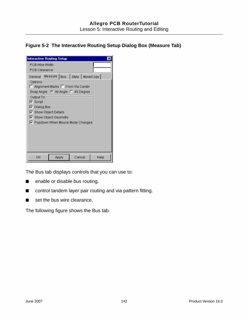
Allegro PCB RouterTutorialLesson 5: Interactive Routing and Editing
Figure 5-2 The Interactive Routing Setup Dialog Box (Measure Tab)
The Bus tab displays controls that you can use to:
■ enable or disable bus routing.
■ control tandem layer pair routing and via pattern fitting.
■ set the bus wire clearance.
The following figure shows the Bus tab.
June 2007 142 Product Version 16.0
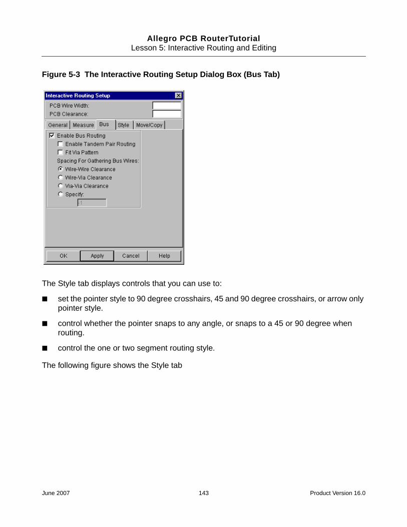
Allegro PCB RouterTutorialLesson 5: Interactive Routing and Editing
Figure 5-3 The Interactive Routing Setup Dialog Box (Bus Tab)
The Style tab displays controls that you can use to:
■ set the pointer style to 90 degree crosshairs, 45 and 90 degree crosshairs, or arrow onlypointer style.
■ control whether the pointer snaps to any angle, or snaps to a 45 or 90 degree whenrouting.
■ control the one or two segment routing style.
The following figure shows the Style tab
June 2007 143 Product Version 16.0

Allegro PCB RouterTutorialLesson 5: Interactive Routing and Editing
Figure 5-4 The Interactive Routing Setup DIalog Box (Style Tab)
The Move/Copy tab displays controls that you can use to:
■ set the default rotation angle and mirroring axis for automatic object rotation andmirroring during move or copy operations.
■ change the incremental rotation angle for incremenetal object rotation.
■ change the incremental mirroring axis for incremental object mirroring.
■ control whether copies of wiring polygons have the same net assignment as the originalor are unassigned (for Copy Polygon mode only).
■ control whether the tool slides the objects, attempting to push obstacles out of the way,or moves them over obstacles and drops them in the new location (for Move mode only).
The following figure shows the Move/Copy tab.
June 2007 144 Product Version 16.0

Allegro PCB RouterTutorialLesson 5: Interactive Routing and Editing
Figure 5-5 The Interactive Routing Setup DIalog Box (Move/Copy Tab)
In this section, you will load a Wires file, which contains routed wires. You will then use theInteractive Routing Setup dialog box to change the pointer style and change the pointer snapangle, which will affect the interactive routing environment. Next, you will route a connectionto see how EditRoute pushes wires aside as you are routing.
Task: Load a wires file
Procedure
1. Start PCB Router and load lesson5a.dsn from the tutorial directory. See Whereto find the Accompanying Lesson Files on page 12 for the location of this directory.
2. Choose File – Read – Wires.
The Read Wires dialog box opens.
3. Click the Browse button.
The Open dialog box opens for Windows platforms.
The Select File dialog box opens for UNIX platforms.
June 2007 145 Product Version 16.0
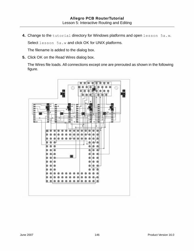
Allegro PCB RouterTutorialLesson 5: Interactive Routing and Editing
4. Change to the tutorial directory for Windows platforms and open lesson 5a.w.
Select lesson 5a.w and click OK for UNIX platforms.
The filename is added to the dialog box.
5. Click OK on the Read Wires dialog box.
The Wires file loads. All connections except one are prerouted as shown in the followingfigure.
June 2007 146 Product Version 16.0
Allegro PCB RouterTutorialLesson 5: Interactive Routing and Editing
Task: Set up your interactive routing and editing environment
Click on the following link to see how this is done before attempting the task on your own.
Show me
This demonstration runs in your browser for approximately 1 minute and 48 seconds.
Procedure
1. Move the pointer into the work area and press the right mouse button.
The Interactive Routing Menu appears.
2. Choose Setup from the Interactive Routing Menu.
The Interactive Routing Setup dialog box opens.
3. Click on the Style tab.
4. Set the pointer style to a 90 degree crosshair and the pointer snap angle to 90 degreesby doing the following:
a. Select 90 Degree Crosshair for the Pointer Style.
b. Select 90 Degrees for the Pointer Snap.
c. Click OK.
5. Display reference designators and pin ID’s by doing the following:
a. Click View – Labels.
The View Labels dialog box opens.
b. Select Ref Des and Pin ID’s.
c. Click OK.
The Reference designators display with the components.
Task: Route a connection using Edit Route
Click on the following link to see how this is done before attempting the task on your own.
Show me
This demonstration runs in your browser for approximately 4 minutes and 50 seconds.
June 2007 147 Product Version 16.0

Allegro PCB RouterTutorialLesson 5: Interactive Routing and Editing
Procedure
1. Zoom in to view the unrouted connection of U4-16 to U5.
You will route the unrouted connection of U4-16 to U5 using Edit Route mode.
2. Press the right mouse button and choose Edit Route Mode.
A pointer appears in the work area and Edit Route appears in the mode status area.
3. Click pin 16 on U4.
4. The pointer changes to 90 degree crosshairs.
5. Press the right mouse button and choose Cancel.
The routing operation stops. Edit Route still appears in the mode status area.
The crosshairs do not display unless you are routing a connection.
6. Click on U4-16 and route the connection out of the right side of the pin and down half thedistance to the target pin on U5. Zoom in if necessary.
The route adds unnecessary angles to the surrounding wires. You will learn how toremove unnecessary angles from wires by using Critic Route later in this lesson. You willignore these angles for now.
Note: If you make a mistake, you can press the right mouse button and choose Undo toundo the last action or Cancel to cancel the last command.
7. Press the right mouse button and choose Setup.
8. Click 45 Degree Crosshair for the Pointer Style.
9. Click 45 Degrees for the Pointer Snap.
10. Click OK.
The pointer appears as both 45 and 90 degree crosshairs.
11. Use a 45 degree corner to finish routing the connection to U5.
When you click the target pin on U5, the connection completes, and the wire disconnectsfrom the pointer.
12. Type quit in the command entry area to exit PCB Router.
You do not need to save the Session file or the Did file.
June 2007 148 Product Version 16.0
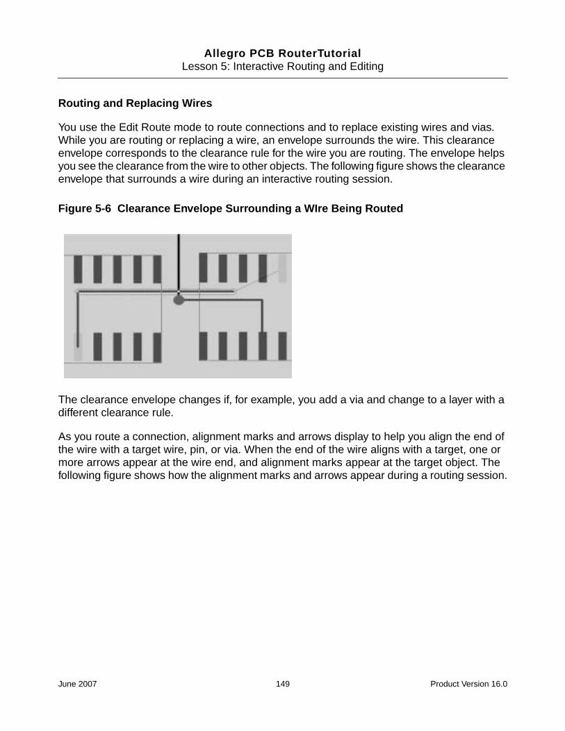
Allegro PCB RouterTutorialLesson 5: Interactive Routing and Editing
Routing and Replacing Wires
You use the Edit Route mode to route connections and to replace existing wires and vias.While you are routing or replacing a wire, an envelope surrounds the wire. This clearanceenvelope corresponds to the clearance rule for the wire you are routing. The envelope helpsyou see the clearance from the wire to other objects. The following figure shows the clearanceenvelope that surrounds a wire during an interactive routing session.
Figure 5-6 Clearance Envelope Surrounding a WIre Being Routed
The clearance envelope changes if, for example, you add a via and change to a layer with adifferent clearance rule.
As you route a connection, alignment marks and arrows display to help you align the end ofthe wire with a target wire, pin, or via. When the end of the wire aligns with a target, one ormore arrows appear at the wire end, and alignment marks appear at the target object. Thefollowing figure shows how the alignment marks and arrows appear during a routing session.
June 2007 149 Product Version 16.0

Allegro PCB RouterTutorialLesson 5: Interactive Routing and Editing
Figure 5-7 Alignment Marks and Arrows on a Wire Being Routed
You will use Edit Route mode to route several connections. As you route each connection,use the clearance envelope to help you route the wires as close together as possible withoutcreating clearance violations. Use the alignment marks and arrows to make straightconnections to the target pins.
Task: Interactively route several connections
Procedure
1. Start PCB Router and load lesson5b.dsn from the tutorial directory.
2. Display the reference designators and pin ID’s by doing the following:
a. Click View – Labels.
The View Labels dialog box displays.
b. Select Ref Des and Pin IDs.
c. Click OK.
The Reference designators display with the components.
June 2007 150 Product Version 16.0

Allegro PCB RouterTutorialLesson 5: Interactive Routing and Editing
3. Move the pointer into the work area and press the right mouse button.
The Interactive Route dialog box opens.
4. Choose Edit Route Mode from the Interactive Routing menu.
Edit Route appears in the mode status area.
5. Zoom in to view U4 and U5.
6. Route the six connections between U4 and U5, as shown in the following figure.
7. Type quit in the command entry area to exit PCB Router.
You immediately exit PCB Router without saving a Session file. The Did file remains inthe tutorial directory. You will not need the Did file, so you can delete it.
Next you will learn how to finish an unrouted or partially routed connection.
Finishing the Routing
While you are routing in Edit Route mode, you can finish an unrouted or partially routedconnection by choosing Finish Route from the right button menu. Finish Route adds wiresegments and vias, if required, to complete a connection.
Finish Route searches for a path within a limited area around the connection you are routing.If a path cannot be found in the search area, the connection cannot be finished automaticallyand the operation is aborted.
In the following procedure, you finish several connections using the Finish Route option inEdit Route mode.
June 2007 151 Product Version 16.0

Allegro PCB RouterTutorialLesson 5: Interactive Routing and Editing
Task: Finish routing connections
Procedure
1. Start PCB Router and load lesson5b.dsn from the tutorial directory.
2. Display the reference designators and pin IDs.
3. Click the Edit Route button on the tool bar.
Edit Route appears in the mode status area.
4. Zoom in to U4, U5, and the lower half of U6.
5. Click on one of the pins in the upper row of U4.
6. Digitize a portion of the connection above U4.
7. Press the right mouse button and choose Finish Route.
The connection is completed for you.
8. Click on another unrouted pin in the upper row of U4.
9. Press the right mouse button and choose Finish Route.
The connection routes automatically.
You will route the remaining unrouted pins on the upper row of U4. You could do this byselecting each pin and repeating the previous step, but you will learn a faster way to routethese connections by completing the following steps.
10. Click on another unrouted pin in the upper row of U4.
11. Press [Ctrl-A].
Using these two keys, you can repeat the last menu command. In this step, you repeatedstep 9.
12. Repeat steps 10 and 11 to route the remaining unrouted pins on the upper row of U4.
13. Exit the autorouter by choosing File – Quit or by typing quit in the command entryarea.
You do not need to save a Session file or the Did file.
June 2007 152 Product Version 16.0
Allegro PCB RouterTutorialLesson 5: Interactive Routing and Editing
Reversing and Restoring Interactive Operations
If you make a mistake, PCB Router lets you undo a previous interactive routing function. Ifyou did not intend to undo something, you can restore it using the redo command. Thefollowing table shows how to use the undo and redo commands.
Table 5-1 Undo and Redo Functions for Interactive Routing
Note: You can undo an individual or a series of interactive functions. However, if you interruptan interactive routing, editing, or placement session with a select, report, autorouting orautoplacement function; undo and redo memory is cleared and you cannot undo or redo priorfunctions.
The following procedure uses undo and redo to reverse and then restore interactive routingfunctions.
Task: Use undo and redo to reverse and restore interactive routing
Procedure
1. Start PCB Router and load lesson5c.dsn from the tutorial directory.
2. Press the right button menu and choose Setup from the Interactive Routing menu.
Function Description Execute by . . .
undo Reverses the last interactivefunction.
Pressing the F3 function key
- or -
Choosing Undo from the right buttonmenu.
- or -
Choosing Edit – Undo from themenu bar
redo Restores the last interactivefunction reversed with undo.
Holding down the [Shift] key andpressing F3.
- or -
Choosing Edit – Redo from themenu bar.
June 2007 153 Product Version 16.0

Allegro PCB RouterTutorialLesson 5: Interactive Routing and Editing
The Interactive Routing Setup dialog box opens.
3. Click on the the Style tab and do the following.
a. Click 90 Degree Crosshair for the Pointer Style.
b. Click OK.
4. Click the Edit Route button on the tool bar.
Edit Route appears in the mode status area.
5. Display the reference designators.
6. Route several connections between U2 and U3 as shown in the following figure.
7. Press F3 to undo the last function.
8. Press [Shift]F3 to redo the function you reversed with undo.
9. Complete all the connections between U2 and U3
10. Use F3 to undo all previous routing steps.
11. Use [Shift]F3 to restore all the routing you removed with undo.
12. Exit PCB Router without saving a Session file or a Did file.
June 2007 154 Product Version 16.0
Allegro PCB RouterTutorialLesson 5: Interactive Routing and Editing
Adding Vias and Changing Layers
While you are interactively routing, the layer you are routing on is the primary layer. Thelayers that you can change to when you add a via are the secondary layers. The primarylayer is always named on the status bar in the area beside the pencil button.
If you add a via and change to a different routing layer, the layer you change to becomes theprimary layer and the previous routing layer becomes a secondary layer. You control the initialprimary and secondary routing layers by using the Layers panel. In the Layer panel, you candisable layers if you do not want to use them during interactive routing.
A pencil button in the Layer panel identifies whether a signal layer is the primary layer or asecondary layer. The bold pencil identifies the primary layer. A dim pencil identifies asecondary layer. If neither the dim nor bold pencil appears for a signal layer, the layer isdisabled for interactive routing.
The following figure shows the Layer panel with L1 as the primary layer and L2, L3, and L4as secondary layers.
June 2007 155 Product Version 16.0

Allegro PCB RouterTutorialLesson 5: Interactive Routing and Editing
Figure 5-8 The Layers Panel
June 2007 156 Product Version 16.0

Allegro PCB RouterTutorialLesson 5: Interactive Routing and Editing
You set a layer as primary, secondary, or disabled by clicking on the pencil. If you click on adimmed pencil, the layer becomes primary. If you click a second time, the pencil box isemptied and the layer is disabled for interactive routing.
After you choose which layer is primary, which layers are secondary, and whether layers aredisabled, you use the mouse or function keys to add vias and change the routing layer. Thelayer you change to when you add a via depends on how you set up layers as primary,secondary, or disabled.
When you digitize twice at the end of a wire segment, the autorouter adds a via, determinesan optimum secondary layer, and changes to that layer. Instead of allowing the autorouter tochoose the layer, you can choose the layer change by using the F5 and F6 function keys.
The F5 key adds a via and changes routing to the next available layer below the currentrouting layer. Each time you press F5, the next active signal layer becomes the current routinglayer. If you press F5 and no layer is available below the current routing layer, the systembeeps and the message “No enabled layer below <layer id>” displays in the messagearea.
The F6 key adds a via and changes routing to the next available layer above the currentrouting layer. Each time you press F6, you move up to the next available signal layer. If nolayer is available above the current routing layer, the system beeps and a warning messageappears in the message area.
In the following procedure, you set up the primary and secondary routing layers, disable twosignal layers for interactive routing, and use the F5 and F6 function keys to add a via.
Task: Set up the routing layers and use function keys to change layers and add a via
Procedure
1. Start PCB Router and load lesson5d.dsn from the tutorial directory.
2. Click the Layer button on the tool bar.
The Layer panel opens, as shown in the following figure. You will disable layers L2 andL3.
3. Click twice in each pencil box to disable layers L2 and L3.
June 2007 157 Product Version 16.0

Allegro PCB RouterTutorialLesson 5: Interactive Routing and Editing
The pencil boxes for layers L2 and L3 are empty, which means these layers are disabled.
4. Click Close.
June 2007 158 Product Version 16.0

Allegro PCB RouterTutorialLesson 5: Interactive Routing and Editing
5. Display the reference designators.
6. Click the Edit Route button on the tool bar.
Edit Route appears in the mode status area and L1 appears on the status bar as theprimary layer.
7. Click on pin 1 which is the square pin of P1.
Note: You will need to zoom in to see pin 1.
8. Move the crosshairs a small distance to the right and away from the pin.
9. Press F5.
The wire changes to L4 which is the next available layer below L1 (remember that youdisabled L2 and L3). L4 appears in the status area as the primary layer.
10. Press F5 again.
The message area indicates that no additional layers are available below the currentlayer.
11. Press F6.
The wire changes to L1 which is the available layer above L4.
12. Press F5 to set the primary layer to L4.
13. Digitize a wire segment that ends just above the target pin on U3.
14. Press F6.
A via is added. The primary layer changes to L1.
15. Finish routing the connection to U3.
16. Exit PCB Router.
You do not need to save a Session file or the Did file.
Editing Wires and Vias
You edit wires and vias by setting one of the following editing modes for the left mouse button.
■ Move
■ Copy Route
■ Critic Route
June 2007 159 Product Version 16.0

Allegro PCB RouterTutorialLesson 5: Interactive Routing and Editing
■ Change Via
■ Change Wire Width
You set an editing mode by clicking the right mouse button and choosing the mode from theInteractive Routing menu or by clicking a button on the tool bar.
When you edit wires and vias, PCB Router observes clearance rules if Checking is enabledon the status bar. If Checking is enabled, and you attempt an edit that violates a clearancerule, the function is ignored.
Moving Wires and Vias
You use Move Route mode to move wire segments and vias. As you move a wire segment,the segment stretches at its corners and at the points where it attaches to pins and vias.
If you move a wire segment against a component pin, and Allow Jogs is enabled on theGeneral tab in the Interactive Routing Setup dialog box, the segment “jogs” around the pin ifpossible. When you move a wire against another, or against a via (and Push Routing isenabled on the General tab in the Interactive Routing Setup dialog box), the stationary wireor via is pushed to avoid a clearance violation.
If you move a via, the attached wires stretch to follow. You cannot move a via to a location thatcreates a clearance violation if Checking is enabled in the status bar.
If you move a via against a wire and Push Routing is enabled on the General tab in theInteractive Routing Setup dialog box), the wire “deforms” around the via to avoid a clearanceviolation. If you move a via against a second via, the second via is pushed to avoid a violation.
Next you will use Move mode to move wires and vias. You will see how Move mode workswith Push Routing enabled and disabled.
Task: Move wires and vias with Push Routing enabled and disabled
Procedure
1. Start PCB Router and load lesson5e.dsn from the tutorial directory.
2. Display the reference designators.
3. Zoom in on DS1, U4, U5, and on the via above U4.
4. Click the Move button on the tool bar.
June 2007 160 Product Version 16.0
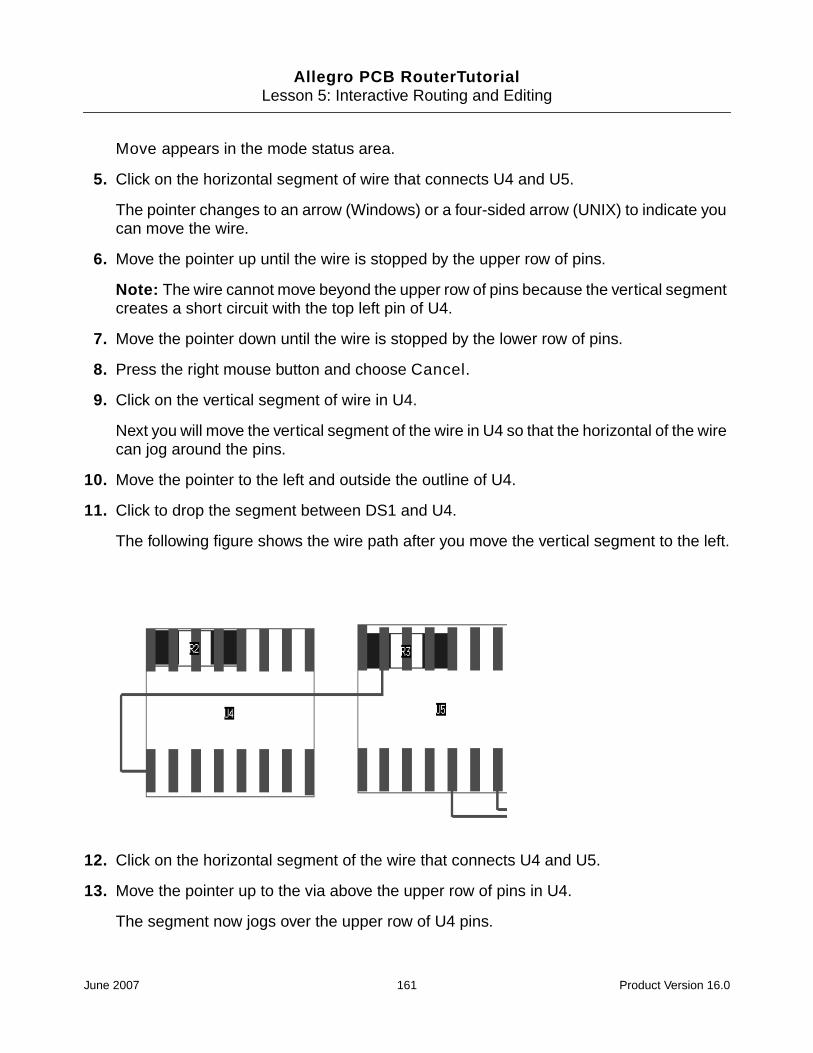
Allegro PCB RouterTutorialLesson 5: Interactive Routing and Editing
Move appears in the mode status area.
5. Click on the horizontal segment of wire that connects U4 and U5.
The pointer changes to an arrow (Windows) or a four-sided arrow (UNIX) to indicate youcan move the wire.
6. Move the pointer up until the wire is stopped by the upper row of pins.
Note: The wire cannot move beyond the upper row of pins because the vertical segmentcreates a short circuit with the top left pin of U4.
7. Move the pointer down until the wire is stopped by the lower row of pins.
8. Press the right mouse button and choose Cancel.
9. Click on the vertical segment of wire in U4.
Next you will move the vertical segment of the wire in U4 so that the horizontal of the wirecan jog around the pins.
10. Move the pointer to the left and outside the outline of U4.
11. Click to drop the segment between DS1 and U4.
The following figure shows the wire path after you move the vertical segment to the left.
12. Click on the horizontal segment of the wire that connects U4 and U5.
13. Move the pointer up to the via above the upper row of pins in U4.
The segment now jogs over the upper row of U4 pins.
June 2007 161 Product Version 16.0
Allegro PCB RouterTutorialLesson 5: Interactive Routing and Editing
14. Move the pointer back down until the wire is stopped by the lower row pins in U4.
Notice how the segment jogs around each pin in the row.
15. Press the right mouse button and choose Cancel.
16. Press the right mouse button and choose Setup from the Interactive Routing menu.
The Interactive Routing Setup dialog box appears.
17. Unselect Push Routing on the General tab to disable Push Routing.
18. Click Apply.
19. Drag the Interactive Routing Setup dialog box to the side of the screen and out of the way.
20. Click on the horizontal segment of the wire that connects U4 and U5.
21. Move the pointer up.
Note: The wire is stopped by the upper row of pins because Push Routing is disabled.
22. Press the right mouse button and notice that Allow Jog Diagonal is disabled.
23. Choose Cancel.
24. Select the Push Routing option in the Interactive Routing Setup dialog box on theGeneral tab and click OK to enable Push Routing.
25. Click on the horizontal segment of the wire that connects U4 and U5 and move thepointer up to the via above U4.
The wire segment attached to the pointer pushes the via.
26. Press the right mouse button and choose Cancel.
27. Exit PCB Router.
You do not need to save a Session file or the Did file.
Copying Wires
You copy wires by using Copy Route mode, which you set by clicking the right mouse buttonand choosing Copy Route Mode from the Interactive Routing Menu or by clicking the CopyRoute button on the tool bar.
You set an editing mode by choosing the mode from the Interactive Routing Menu or byclicking a button on the tool bar.
June 2007 162 Product Version 16.0

Allegro PCB RouterTutorialLesson 5: Interactive Routing and Editing
With Copy Route mode set, click on the wire or on a pin attached to the wire you want to copy.Then click on the target pin you want to route with the copied wire. The target connectionsmust be unrouted and you must be able to wire target connections with the same wire pathas the connection you copy. If the paths of the copied connection and the target connectionare different, the copy function fails and the message “Path cannot be copied” appears inthe Message area.
You will copy a wire path and click on an adjacent pin to replicate the path. You can also dragthe pointer across several pins to replicate the wire path to multiple connections in a singleoperation.
Task: Copy a wire path to several unrouted connections
Procedure
1. Start PCB Router and load lesson5f.dsn from the tutorial directory.
2. Display the reference designators.
3. Zoom in on U4 and U5.
4. Click the Copy Route button on the tool bar.
5. Click on the wire that connects U4 and U5.
The wire is copied to memory and is highlighted.
6. Click on the bottom pin in U4 that is next to the pin that is highlighted.
The wire you copied in the previous step is replicated.
7. Drag the pointer across the five adjacent pins to the right.
June 2007 163 Product Version 16.0
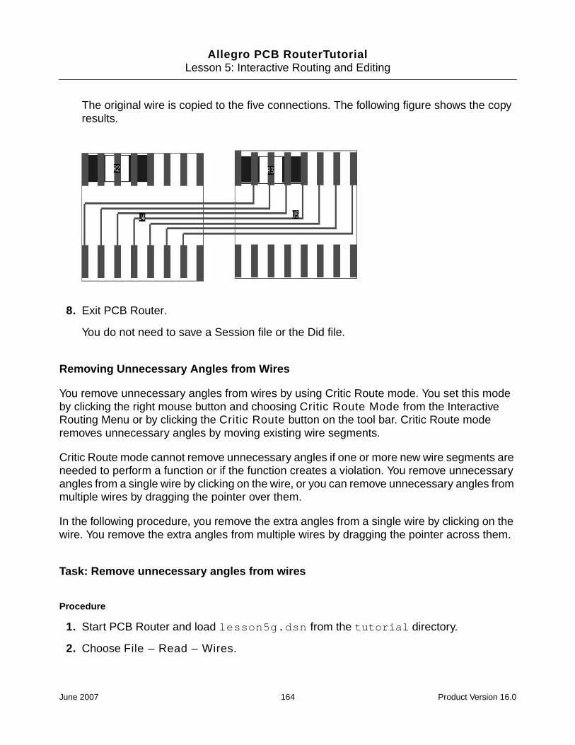
Allegro PCB RouterTutorialLesson 5: Interactive Routing and Editing
The original wire is copied to the five connections. The following figure shows the copyresults.
8. Exit PCB Router.
You do not need to save a Session file or the Did file.
Removing Unnecessary Angles from Wires
You remove unnecessary angles from wires by using Critic Route mode. You set this modeby clicking the right mouse button and choosing Critic Route Mode from the InteractiveRouting Menu or by clicking the Critic Route button on the tool bar. Critic Route moderemoves unnecessary angles by moving existing wire segments.
Critic Route mode cannot remove unnecessary angles if one or more new wire segments areneeded to perform a function or if the function creates a violation. You remove unnecessaryangles from a single wire by clicking on the wire, or you can remove unnecessary angles frommultiple wires by dragging the pointer over them.
In the following procedure, you remove the extra angles from a single wire by clicking on thewire. You remove the extra angles from multiple wires by dragging the pointer across them.
Task: Remove unnecessary angles from wires
Procedure
1. Start PCB Router and load lesson5g.dsn from the tutorial directory.
2. Choose File – Read – Wires.
June 2007 164 Product Version 16.0
Allegro PCB RouterTutorialLesson 5: Interactive Routing and Editing
The Read Wires dialog box opens.
3. Click the Browse button.
4. Choose lesson5g.w from the tutorial directory.
5. Click OK.
The file lesson5g.w appears in the Read Wires data entry box.
6. Click OK.
7. Display the reference designators.
8. Zoom in on U4 and U5.
9. Click the Critic Route button on the tool bar.
10. Click on the wire attached to the lower left pin of U4.
The extra angles are removed from the wire.
11. Drag the pointer across all wires that connect between U4 and U5.
The extra angles are removed from all the wires in a single operation.
12. Exit PCB Router.
You do not need to save a Session file or the Did file.
Replacing Vias with Another Type
You replace an existing via with a different type by using Change Via Mode. You set this modeby clicking the right button menu and choosing Change – Change Via Mode. When you setChange Via mode, a dialog box appears and you must choose which via you want to use toreplace existing vias. The Change Via Setup dialog box, which is shown in the followingfigure, determines the replacement via.
June 2007 165 Product Version 16.0
Allegro PCB RouterTutorialLesson 5: Interactive Routing and Editing
Figure 5-9 Change Via Setup Dialog Box
After initially choosing a replacement via, you can choose a different replacement via bypressing the right mouse button and choosing Setup Change Via.
In the following procedure, you will set Change Via mode, choose a replacement via, replaceseveral existing vias, and then choose a different replacement via.
Task: Set Change Via mode, choose a replacement via, and replace existing vias
Procedure
1. Start PCB Router and load lesson5h.dsn from the tutorial directory.
2. Choose File – Read – Wires.
3. Click the Browse button.
4. Choose lesson5h.w from the tutorial directory.
5. Click OK.
The file lesson5h.w appears in the Read Wires data entry box.
6. Click OK.
7. Display the reference designators.
8. Zoom in on the wiring in the area between U4 and U6.
9. Press the right mouse button and choose Change – Change Via Mode.
June 2007 166 Product Version 16.0

Allegro PCB RouterTutorialLesson 5: Interactive Routing and Editing
The Change Via Setup dialog box opens.
10. Choose square_via from the Via list.
11. Click OK.
Change Via appears in the mode status area.
12. Click on a via that is attached to one of the connections between U4 and U6.
A square via replaces the round via.
13. Press the right mouse button and choose Setup Change Via.
14. Choose round_via from the Vias list.
15. Click OK.
16. Click the square via.
The square via changes to a round via.
17. Exit PCB Router.
You do not need to save a Session file or the Did file.
Changing the Width of an Existing Wire Segment
When you route a connection in PCB Router, whether you are autorouting or interactivelyrouting, wire width is determined by a rule setting. You can change the width of an existingwire segment without setting a rule by using Change Wire mode. You choose this mode byclicking the right mouse button and choosing Change – Change Wire Width Mode fromthe Interactive Routing menu. The Change Wire Setup dialog box is initially displayed asshown in the following figure.
Figure 5-10 Change Wire Setup Dialog Box
After setting the Edit Wire Width value, you can set a different value by clicking right andchoosing Setup Change Wire from the menu.
June 2007 167 Product Version 16.0

Allegro PCB RouterTutorialLesson 5: Interactive Routing and Editing
Change Wire mode changes the width of a wire segment if the action does not create aviolation. If it is determined that changing the width of a wire segment will result in a violation,the action is ignored.
Note: Because Change Wire mode does not set or change a wire width rule, changed widthsare not retained if you reroute the segments. If you want to retain the new widths during anautorouting or rerouting operation, use the protect command to prevent the autorouterfrom altering the wires.
In the following procedure, you will set Change Wire mode and set the edit wire width. Youwill then protect the edited wires to prevent them from changing during subsequentautorouting or rerouting operations.
Task: Set Change Wire mode, change the width and protect the wires
Procedure
1. Start PCB Router and load lesson5i.dsn from the tutorial directory.
2. Display the reference designators.
3. Zoom in on U4 and U5.
4. Click the Edit Route button on the tool bar.
5. Route a short escape wire from the top left pin of U4.
6. Double-click at the end of the escape wire to add a via.
7. Press the right mouse button and choose Done.
A short escape wire and via is routed from the top left pin of U4.
8. Repeat steps 6 and 7 to route the remaining six pins in the top row of U4.
June 2007 168 Product Version 16.0
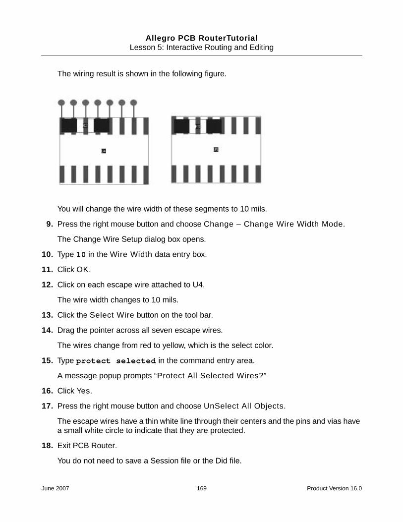
Allegro PCB RouterTutorialLesson 5: Interactive Routing and Editing
The wiring result is shown in the following figure.
You will change the wire width of these segments to 10 mils.
9. Press the right mouse button and choose Change – Change Wire Width Mode.
The Change Wire Setup dialog box opens.
10. Type 10 in the Wire Width data entry box.
11. Click OK.
12. Click on each escape wire attached to U4.
The wire width changes to 10 mils.
13. Click the Select Wire button on the tool bar.
14. Drag the pointer across all seven escape wires.
The wires change from red to yellow, which is the select color.
15. Type protect selected in the command entry area.
A message popup prompts “Protect All Selected Wires?”
16. Click Yes.
17. Press the right mouse button and choose UnSelect All Objects.
The escape wires have a thin white line through their centers and the pins and vias havea small white circle to indicate that they are protected.
18. Exit PCB Router.
You do not need to save a Session file or the Did file.
June 2007 169 Product Version 16.0
Allegro PCB RouterTutorialLesson 5: Interactive Routing and Editing
What You Learned
In this lesson, you learned how to:
■ set up your interactive routing environment.
■ use the routing tools.
■ control the routing layer.
■ add vias as you route.
■ move wiring.
■ copy wiring.
■ eliminate extra angles from a wire.
■ replace a via with another type.
■ change the width of a wire segment.
Congratulations!
You have completed the Allegro PCB Router Tutorial.
If you worked through each lesson in this tutorial, you learned how:
■ the autorouter works.
■ to use the autorouter’s GUI.
■ to place components interactively and automatically.
■ set up the autorouter and analyze early results.
■ set rules and control the autorouter.
■ to route wires automatically.
■ how to use the interactive routing tools.
With the information and procedures you learned, you are ready to begin your own routingprojects.
When you are using PCB Router, remember there is a wealth of information available to youonline. Browse the PCB Router Help menu and explore the manuals. PCB Routerdocumentation is available on a broad range of topics from general information to step-by-step procedures for accomplishing your design tasks.
June 2007 170 Product Version 16.0

Allegro PCB RouterTutorial
Index
Aaligning components 73angles, removing 164autorouting
adaptive method 86analyzing unroutes 115costs 86, 92daisy-chain 130failures
analyzing 114definition of 111
monitoring progress 111phases 91post-routing 98prerouting 91prioritizing nets 136selecting connections 125smart_route 93starburst 130unroute, definition of 111using keepins 128
Bbus command 87, 91bus routing 87
Ccapacitors, placing 78classes of nets 134clean command 87, 92clearance rules 122command file 104commands
autorouting 86bus 87, 91clean 87, 92fanout 87, 91fence 128in do file 104post-routing 98prerouting 91
protect 168recorner 99route 87, 92smart_route 86, 93unselect 126
componentsaligning 73displaying information about 39interchanging 71learning and applying patterns 80locking in place 65moving 79placing
at X,Y locations 57capacitors 78from a list 62large components 66
rotating 63selecting 81
conflictsanalyzing 112, 114causes of 112poor reduction 114types of 86, 111
corners, changing to 45 degrees 99
Ddaisy-chain routing 130design file
definition of 14sections of 17
displayingpower pin labels 78reference designators 57
do file 104
Eediting
changing wire width 167copying wires and vias 162moving wires and vias 160removing unnecessary angles 164
June 2007 171 Product Version 16.0

Allegro PCB RouterTutorial
replacing vias 165rules did file 106, 110
editorrules did file 106
escaping SMD pins 88, 91exiting PCB Router 90
Ffanout command 87, 91fence command 128files
command file 104design file 17do file 104for transferring designs 15placement 83session 83types of 14wires 145
fromtosdefinition of 135selecting 126
function keys, usingfor undo and redo 153to change layers 157
Ggraphical user interface
placement mode 54grids
placement 54routing 93
groups of fromtos 135GUI
placement mode 55
Iimages
definition of 53selecting 81
Interactive Place menu 58interactive routing 140interchanging components 71
Kkeepout areas 66
Llayers
changing primary layer 155selecting for routing 123setting routing direction 123
Layers panel 78, 97, 155license considerations 13load pins, assigning 131locking components 65
Mmoving
components 79wires and vias 160
Nnet classes
assigning routing priority to 136assigning rules to 135defining 134
netsprioritizing for routing 136scheduling for routing 136
Ppairwise interchange operation 71pin sharing 92pins, displaying information about 39placement
grid 54keepout areas 66learning and applying patterns 80mode 54rules 53steps of 52violations 56
placement filecreating 83
June 2007 172 Product Version 16.0
Allegro PCB RouterTutorial
definition of 41loading 74
placing componentsat X,Y locations 57capacitors 78critical components 57from a list 62large components 66small components 78
power pins, displaying 78protect command 168protecting wires 168
Rrecorner command 99reference designators, displaying 57reports,routing status 111rotating components 63route command 87, 92routes file
definition of 15, 41routing
assigning properties 131busses 91classes of nets 134conflict types 86daisy-chain 130failures
analyzing 114definition of 111
in batch mode 104interactively 140keepin regions 128one or more connections 125preventing rerouting 168prioritizing nets 136restricting to area 128rules 100, 118running basic passes 88selecting layers 123selecting vias 124setting layer direction 123starburst 130
routing interactivelyadding vias 155aligning with pins and vias 149finishing automatically 151pushing wires 160redoing an operation 153
setting your environment 140undoing an operation 153
rulesassigning to
groups of fromtos 135net classes 135
clearance 122hierarchy 53placement 53precedence of 53, 100routing 100, 118setting width and clearance 102setting wire and via clearance 121spacing 54width 119
rules did file 106, 110rules did file editor
creating a do file 106
Ssaving
placement file 83selecting
components 81connections for routing 125images 81layers for routing 123vias for routing 124
session filecreating 83definition of 15, 41
smart_route command 86, 93SMD escape 91source pin, assigning 131starburst routing 130status report, routing 111
Tterminator pin, assigning 131transferring designs 15
Uunroute, definition of 111unselect command 126unselecting
June 2007 173 Product Version 16.0

Allegro PCB RouterTutorial
objects 81vias for routing 124
Vvias
adding 155changing 165copying 162displaying information about 40moving 160replacing 165selecting for routing 124setting clearance rules 122sharing 92unselecting for routing 124using blind and buried 125
Wwires
changing width 167copying 162displaying information about 40editing 149moving 160removing unnecessary angles 164setting clearance rules 122
wires file 15, 145
June 2007 174 Product Version 16.0