Embed Size (px)
Citation preview
1
Interaction Note
Note 617
April 2011
Allocating Indirect Lightning to Cables & Boxes at Program InceptionApplication of Ohm’s Law, Kirchhoff’s Laws, Faraday’s Law &
Scaling by Geometric, Electrical, & Spectral Parameters
Larry West10215 Beechnut St, Suite 1003
Houston, TX 77072
abstract
Indirect lightning engineering needs early numbers for allocations of weight and space forprotection in weight conscious composite systems’ programs. This note attempts to do definethe in-flight environments and provide the tools for scaling them to any size system. Waveform5A (WF5A) in the standards has been changed to Waveform 4 (WF4) based on findings in IN615.All other allocations are affected as more high frequency penetrates onto interior conductorsand less on the exterior. Lightning Components A, D, and H have about the same dI/dt and thesame spectra above 2MHz therefore they will excite the same levels of Waveform 2 derivativeexcitation and Waveform 3 resonant excitation. Design guidelines help meet requirements.
2
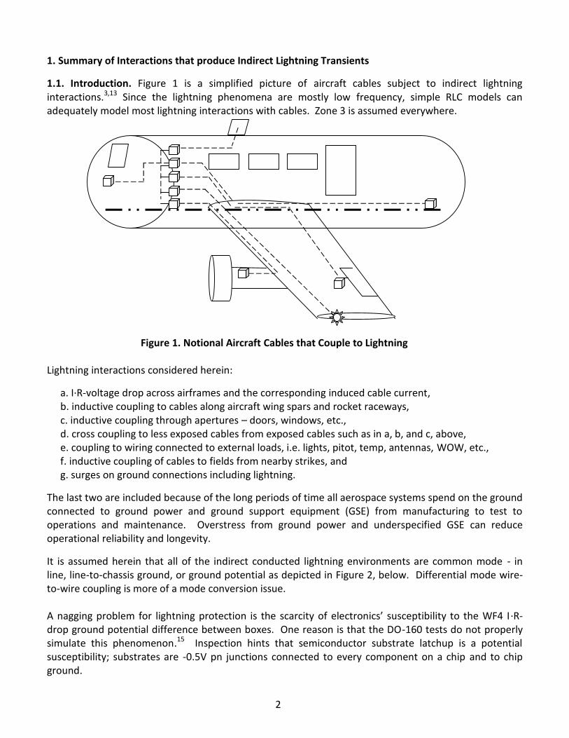
1. Summary of Interactions that produce Indirect Lightning Transients
1.1. Introduction. Figure 1 is a simplified picture of aircraft cables subject to indirect lightninginteractions.3,13 Since the lightning phenomena are mostly low frequency, simple RLC models canadequately model most lightning interactions with cables. Zone 3 is assumed everywhere.
Figure 1. Notional Aircraft Cables that Couple to Lightning
Lightning interactions considered herein:
a. I∙R-voltage drop across airframes and the corresponding induced cable current,b. inductive coupling to cables along aircraft wing spars and rocket raceways,c. inductive coupling through apertures – doors, windows, etc.,d. cross coupling to less exposed cables from exposed cables such as in a, b, and c, above,e. coupling to wiring connected to external loads, i.e. lights, pitot, temp, antennas, WOW, etc.,f. inductive coupling of cables to fields from nearby strikes, andg. surges on ground connections including lightning.
The last two are included because of the long periods of time all aerospace systems spend on the groundconnected to ground power and ground support equipment (GSE) from manufacturing to test tooperations and maintenance. Overstress from ground power and underspecified GSE can reduceoperational reliability and longevity.
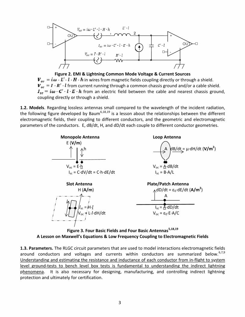
It is assumed herein that all of the indirect conducted lightning environments are common mode - inline, line-to-chassis ground, or ground potential as depicted in Figure 2, below. Differential mode wire-to-wire coupling is more of a mode conversion issue.
A nagging problem for lightning protection is the scarcity of electronics’ susceptibility to the WF4 I∙R-drop ground potential difference between boxes. One reason is that the DO-160 tests do not properlysimulate this phenomenon.15 Inspection hints that semiconductor substrate latchup is a potentialsusceptibility; substrates are -0.5V pn junctions connected to every component on a chip and to chipground.
3
Voc=iwLI
Isc=iwCV C
L1 2
R
+
-
OUT +
-
OUT
Voc=IR
Figure 2. EMI & Lightning Common Mode Voltage & Current Sourcesin wires from magnetic fields coupling directly or through a shield.
from current running through a common chassis ground and/or a cable shield.from an electric field between the cable and nearest chassis ground,
coupling directly or through a shield.
1.2. Models. Regarding lossless antennas small compared to the wavelength of the incident radiation,the following figure developed by Baum6,18,19 is a lesson about the relationships between the differentelectromagnetic fields, their coupling to different conductors, and the geometric and electromagneticparameters of the conductors. E, dB/dt, H, and dD/dt each couple to different conductor geometries.
Monopole Antenna Loop AntennaE (V/m)
h A dB/dt = µ·dH/dt (V/m2)
Voc = E·h Voc = A·dB/dtIsc = C·dV/dt = C·h·dE/dt Isc = B·A/L
Slot Antenna Plate/Patch AntennaH (A/m) dD/dt = ε0·dE/dt (A/m2)
Al
Isc = H·l Isc = A·dD/dtVoc = L·l·dH/dt Voc = ε0·E·A/C
Figure 3. Four Basic Fields and Four Basic Antennas5,18,19
A Lesson on Maxwell’s Equations & Low Frequency Coupling to Electromagnetic Fields
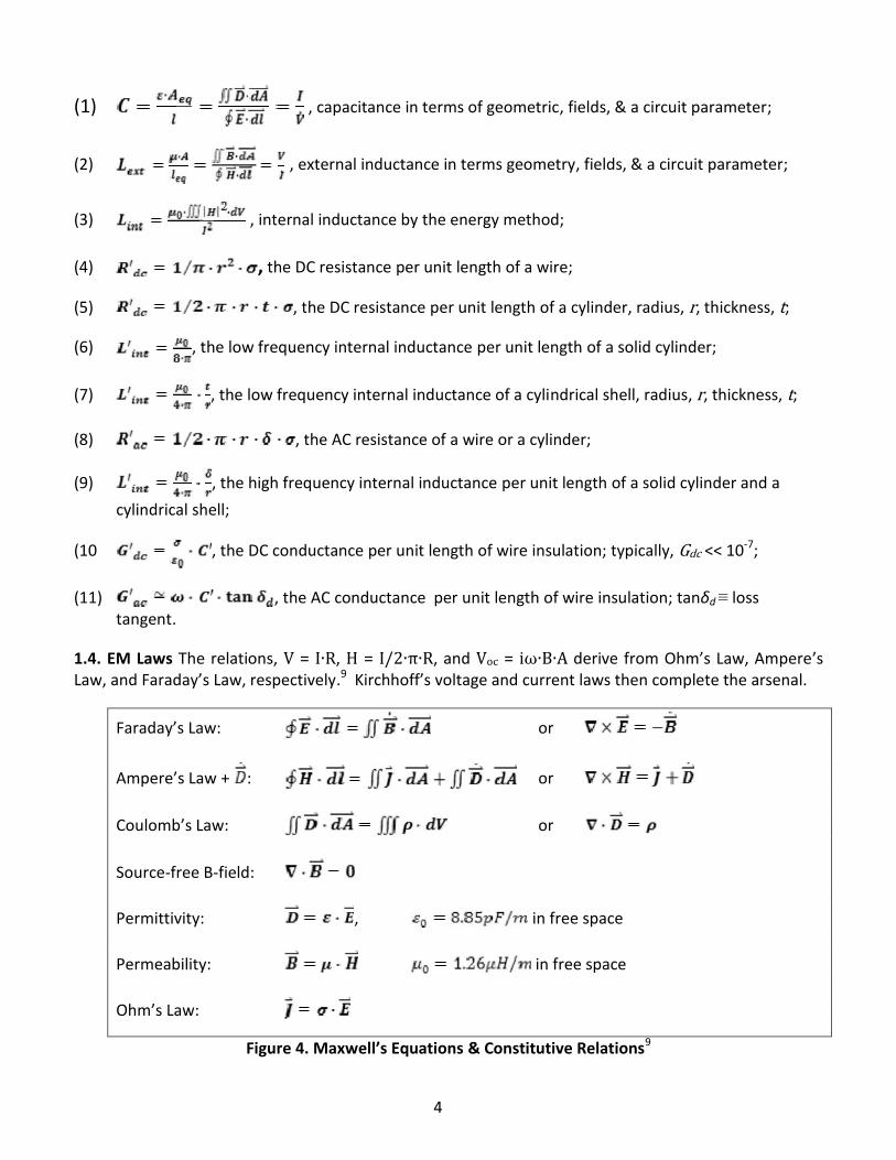
1.3. Parameters. The RLGC circuit parameters that are used to model interactions electromagnetic fieldsaround conductors and voltages and currents within conductors are summarized below.6,7,9
Understanding and estimating the resistance and inductance of each conductor from in-flight to systemlevel ground-tests to bench level box tests is fundamental to understanding the indirect lightningphenomena. It is also necessary for designing, manufacturing, and controlling indirect lightningprotection and ultimately for certification.
4
(1) , capacitance in terms of geometric, fields, & a circuit parameter;
(2) , external inductance in terms geometry, fields, & a circuit parameter;
(3) , internal inductance by the energy method;
(4) , the DC resistance per unit length of a wire;
(5) , the DC resistance per unit length of a cylinder, radius, r, thickness, t;
(6) , the low frequency internal inductance per unit length of a solid cylinder;
(7) , the low frequency internal inductance of a cylindrical shell, radius, r, thickness, t;
(8) , the AC resistance of a wire or a cylinder;
(9) , the high frequency internal inductance per unit length of a solid cylinder and a
cylindrical shell;
(10 , the DC conductance per unit length of wire insulation; typically, Gdc << 10-7;
(11) , the AC conductance per unit length of wire insulation; tanδd ≡ losstangent.
1.4. EM Laws The relations, V = I∙R, H = I/2∙π∙R, and Voc = iω∙B∙A derive from Ohm’s Law, Ampere’sLaw, and Faraday’s Law, respectively.9 Kirchhoff’s voltage and current laws then complete the arsenal.
Faraday’s Law: or
Ampere’s Law + : or
Coulomb’s Law: or
Source-free B-field:
Permittivity: , in free space
Permeability: in free space
Ohm’s Law:
Figure 4. Maxwell’s Equations & Constitutive Relations9
5
1.5. Structural I∙R Voltage Drop
The most unique indirect lightning environment in composite aircraft is the large voltage induced alongthe path of the lightning current through the system. The corresponding cable current is different, also,due to the unique in-flight interaction, and is the focus of Paper #113.
1.5.1. Voltage IR-Drop across the Airframe and Induced Cable Currents and Voltages
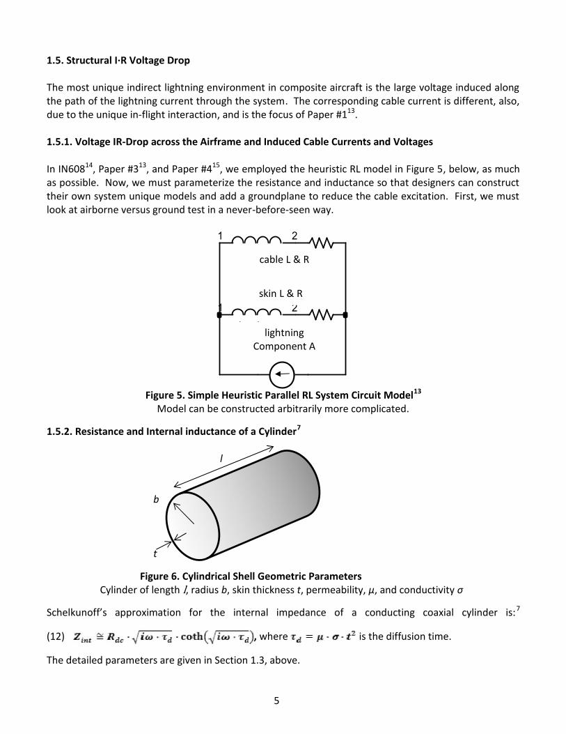
In IN60814, Paper #313, and Paper #415, we employed the heuristic RL model in Figure 5, below, as muchas possible. Now, we must parameterize the resistance and inductance so that designers can constructtheir own system unique models and add a groundplane to reduce the cable excitation. First, we mustlook at airborne versus ground test in a never-before-seen way.
low R
high R
high L
1 2
low L
1 2
I1
CFC skin
All Internal Metal Lines
lightning Waveform AFigure 5. Simple Heuristic Parallel RL System Circuit Model13
Model can be constructed arbitrarily more complicated.
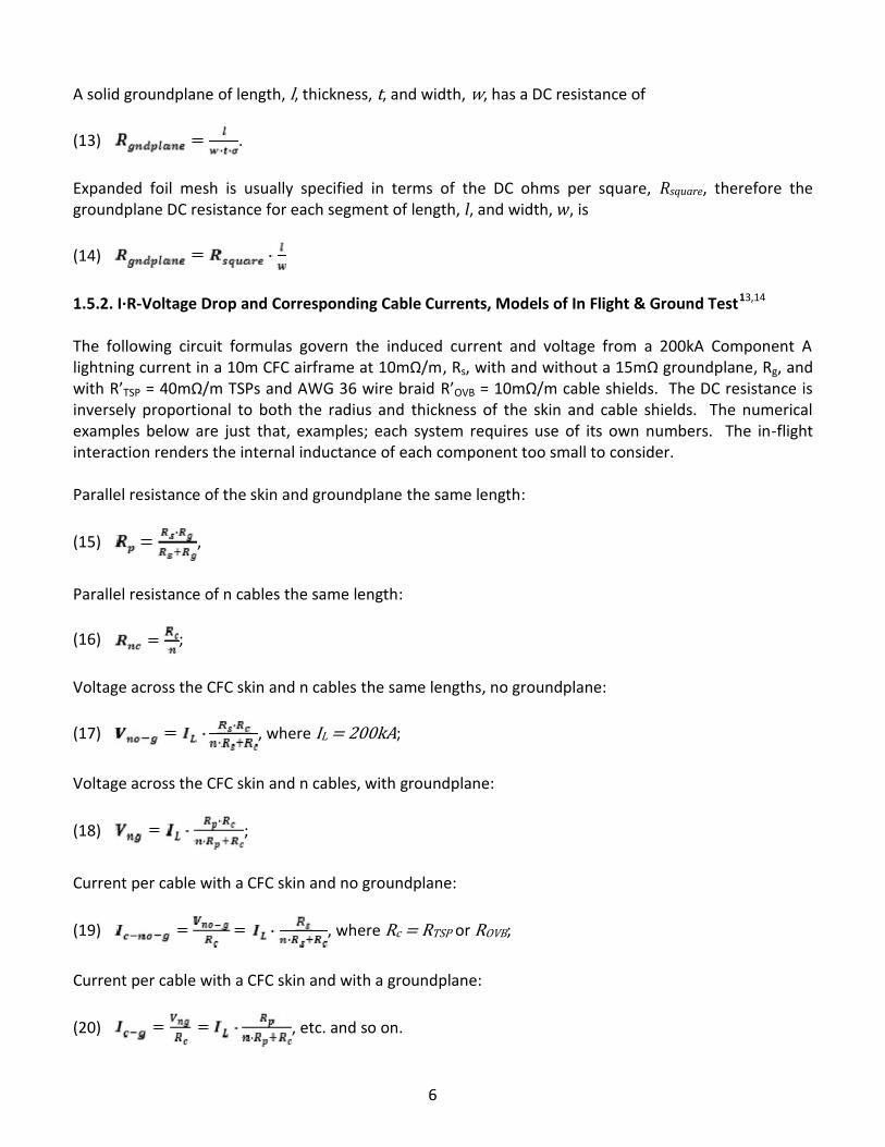
1.5.2. Resistance and Internal inductance of a Cylinder7
l
b
t
Figure 6. Cylindrical Shell Geometric ParametersCylinder of length l, radius b, skin thickness t, permeability, µ, and conductivity σ
Schelkunoff’s approximation for the internal impedance of a conducting coaxial cylinder is:7
(12) , where is the diffusion time.
The detailed parameters are given in Section 1.3, above.
cable L & R
skin L & R
lightningComponent A
6
A solid groundplane of length, l, thickness, t, and width, w, has a DC resistance of
(13) .
Expanded foil mesh is usually specified in terms of the DC ohms per square, Rsquare, therefore thegroundplane DC resistance for each segment of length, l, and width, w, is
(14)
1.5.2. I∙R-Voltage Drop and Corresponding Cable Currents, Models of In Flight & Ground Test13,14
The following circuit formulas govern the induced current and voltage from a 200kA Component Alightning current in a 10m CFC airframe at 10mΩ/m, Rs, with and without a 15mΩ groundplane, Rg, andwith R’TSP = 40mΩ/m TSPs and AWG 36 wire braid R’OVB = 10mΩ/m cable shields. The DC resistance isinversely proportional to both the radius and thickness of the skin and cable shields. The numericalexamples below are just that, examples; each system requires use of its own numbers. The in-flightinteraction renders the internal inductance of each component too small to consider.
Parallel resistance of the skin and groundplane the same length:
(15) ,
Parallel resistance of n cables the same length:
(16) ;
Voltage across the CFC skin and n cables the same lengths, no groundplane:
(17) , where IL = 200kA;
Voltage across the CFC skin and n cables, with groundplane:
(18) ;
Current per cable with a CFC skin and no groundplane:
(19) , where Rc = RTSP or ROVB;
Current per cable with a CFC skin and with a groundplane:
(20) , etc. and so on.
7
The following examples use these parameters: , ,
, and , all scaled by the ratio of
length/(width or radius x thickness x conductivity) for the reader that has different parameters.
1.5.2.2. Waveforms & Current Division, In-Flight versus Ground-Test with No Groundplane
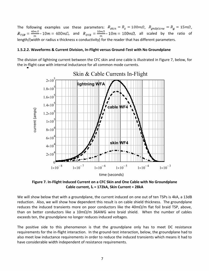
The division of lightning current between the CFC skin and one cable is illustrated in Figure 7, below, forthe in-flight case with internal inductance for all common mode currents.
1 10 8 1 10 7 1 10 6 1 10 5 1 10 4 1 10 30
2 104
4 104
6 104
8 104
1 105
1.2 105
1.4 105
1.6 105
1.8 105
2 105
Skin & Cable Currents In-Flight
Is1 n( )
Ic1 n( )
IL n( )
t n( )
lightning WFA
cable WF4
skin WF4
Figure 7. In-Flight Induced Current on a CFC Skin and One Cable with No GroundplaneCable current, It = 172kA, Skin Current = 28kA
We will show below that with a groundplane, the current induced on one out of ten TSPs is 4kA, a 13dBreduction. Also, we will show how dependent this result is on cable shield thickness. The groundplanereduces the induced transients more on poor conductors like the 40mΩ/m flat foil braid TSP, above,than on better conductors like a 10mΩ/m 36AWG wire braid shield. When the number of cablesexceeds ten, the groundplane no longer reduces induced voltages.
The positive side to this phenomenon is that the groundplane only has to meet DC resistancerequirements for the in-flight interaction. In the ground-test interaction, below, the groundplane had toalso meet low inductance requirements in order to reduce the induced transients which means it had tohave considerable width independent of resistance requirements.
curr
ent (
amps
)
time (seconds)
8
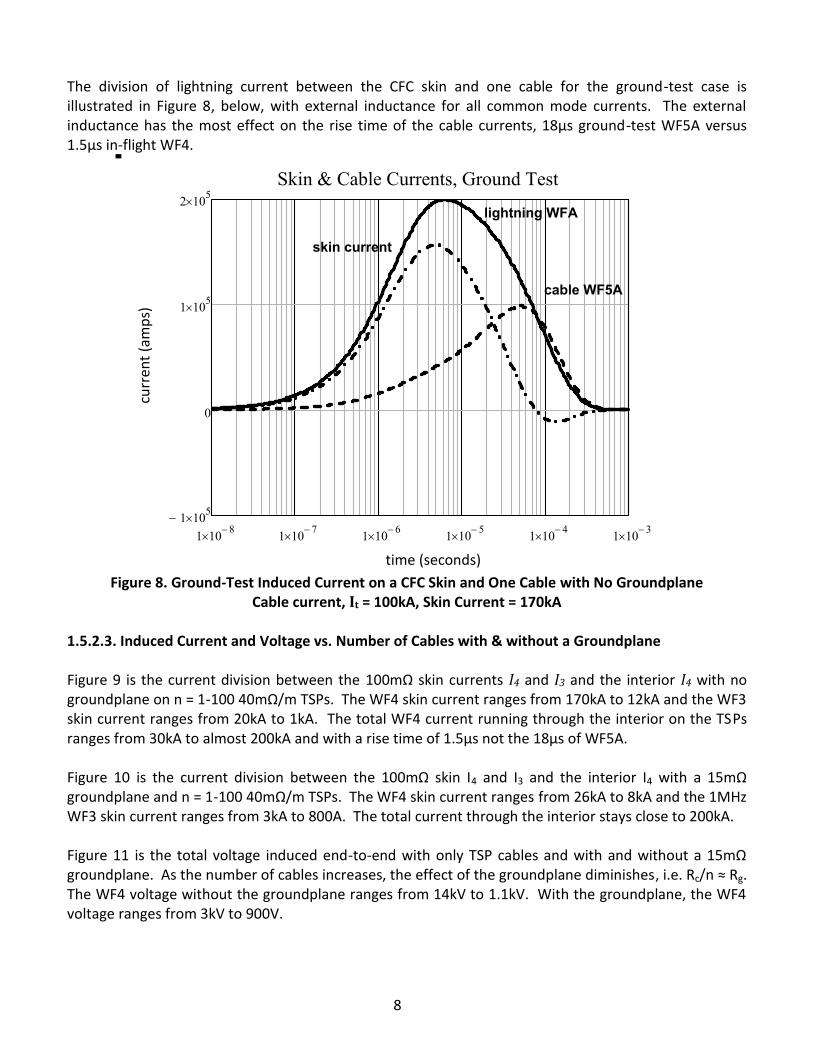
The division of lightning current between the CFC skin and one cable for the ground-test case isillustrated in Figure 8, below, with external inductance for all common mode currents. The externalinductance has the most effect on the rise time of the cable currents, 18µs ground-test WF5A versus1.5µs in-flight WF4.
1 10 8 1 10 7 1 10 6 1 10 5 1 10 4 1 10 31 105
0
1 105
2 105
Skin & Cable Currents, Ground Test
Isg n( )
Icg n( )
IL n( )
IT n( )
t n( )
lightning WFA
skin current
cable WF5A
Figure 8. Ground-Test Induced Current on a CFC Skin and One Cable with No GroundplaneCable current, It = 100kA, Skin Current = 170kA
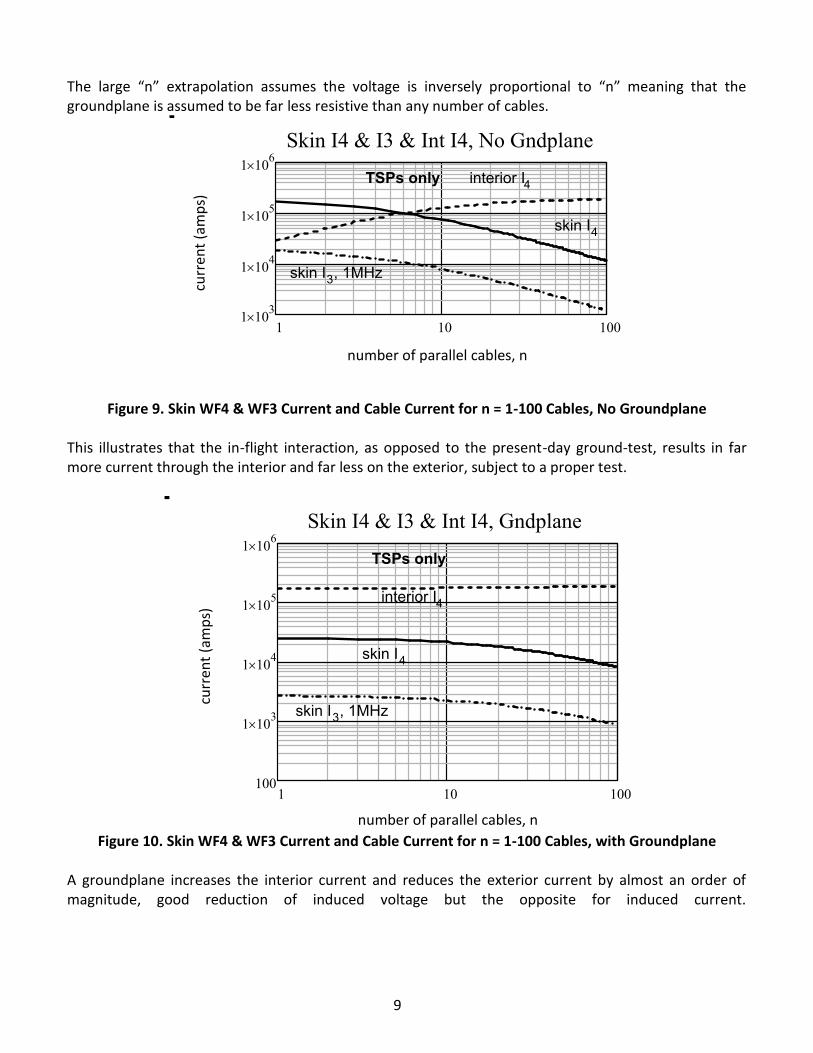
1.5.2.3. Induced Current and Voltage vs. Number of Cables with & without a Groundplane
Figure 9 is the current division between the 100mΩ skin currents I4 and I3 and the interior I4 with nogroundplane on n = 1-100 40mΩ/m TSPs. The WF4 skin current ranges from 170kA to 12kA and the WF3skin current ranges from 20kA to 1kA. The total WF4 current running through the interior on the TSPsranges from 30kA to almost 200kA and with a rise time of 1.5μs not the 18μs of WF5A.
Figure 10 is the current division between the 100mΩ skin I4 and I3 and the interior I4 with a 15mΩgroundplane and n = 1-100 40mΩ/m TSPs. The WF4 skin current ranges from 26kA to 8kA and the 1MHzWF3 skin current ranges from 3kA to 800A. The total current through the interior stays close to 200kA.
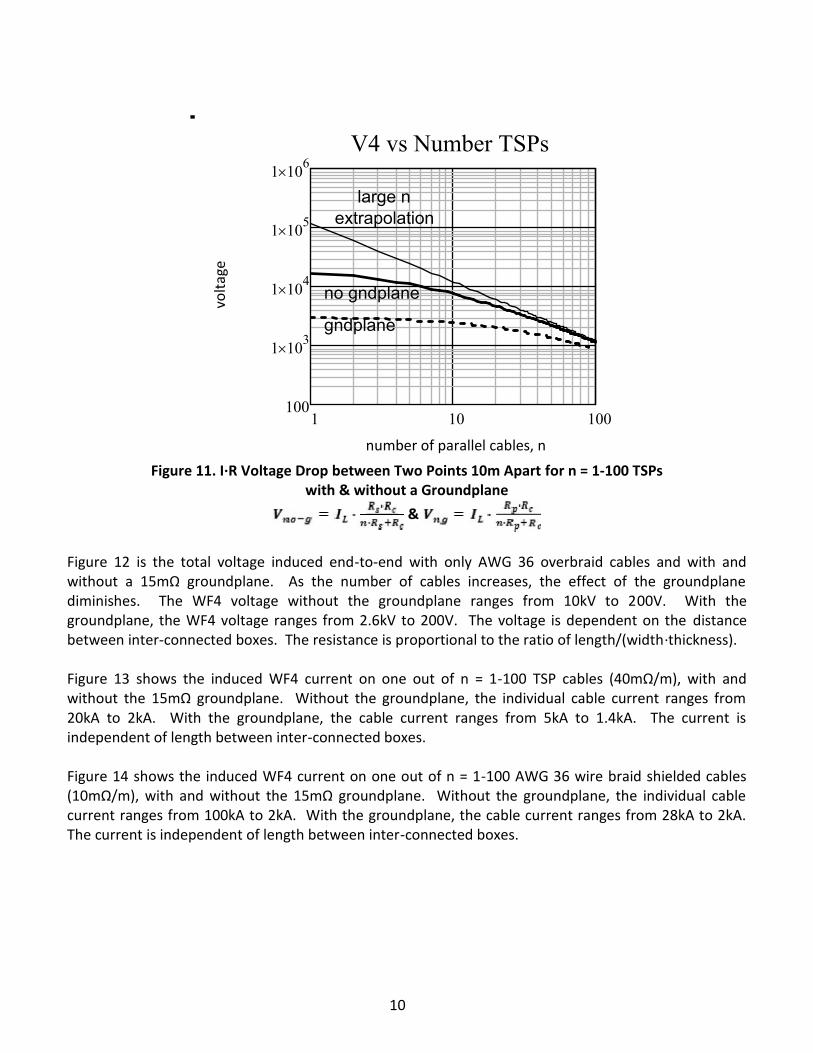
Figure 11 is the total voltage induced end-to-end with only TSP cables and with and without a 15mΩgroundplane. As the number of cables increases, the effect of the groundplane diminishes, i.e. Rc/n ≈ Rg.The WF4 voltage without the groundplane ranges from 14kV to 1.1kV. With the groundplane, the WF4voltage ranges from 3kV to 900V.
time (seconds)
curr
ent (
amps
)
9
The large “n” extrapolation assumes the voltage is inversely proportional to “n” meaning that thegroundplane is assumed to be far less resistive than any number of cables.
1 10 1001 103
1 104
1 105
1 106
Skin I4 & I3 & Int I4, No Gndplane
Isc1 n( )
Iint1 n( )
I3s1 n( )
n
TSPs only interior I4
skin I4
skin I3, 1MHz
Figure 9. Skin WF4 & WF3 Current and Cable Current for n = 1-100 Cables, No Groundplane
This illustrates that the in-flight interaction, as opposed to the present-day ground-test, results in farmore current through the interior and far less on the exterior, subject to a proper test.
1 10 100100
1 103
1 104
1 105
1 106
Skin I4 & I3 & Int I4, Gndplane
Isg1 n( )
Iintg1 n( )
I3sg1 n( )
n
TSPs only
interior I4
skin I4
skin I3, 1MHz
Figure 10. Skin WF4 & WF3 Current and Cable Current for n = 1-100 Cables, with Groundplane
A groundplane increases the interior current and reduces the exterior current by almost an order ofmagnitude, good reduction of induced voltage but the opposite for induced current.
curr
ent (
amps
)
number of parallel cables, n
curr
ent (
amps
)
number of parallel cables, n
10
1 10 100100
1 103
1 104
1 105
1 106
V4 vs Number TSPs
V4s1 n( )
V4g1 n( )
V4c1 n( )
n
large nextrapolation
no gndplane
gndplane
Figure 11. I·R Voltage Drop between Two Points 10m Apart for n = 1-100 TSPswith & without a Groundplane
&
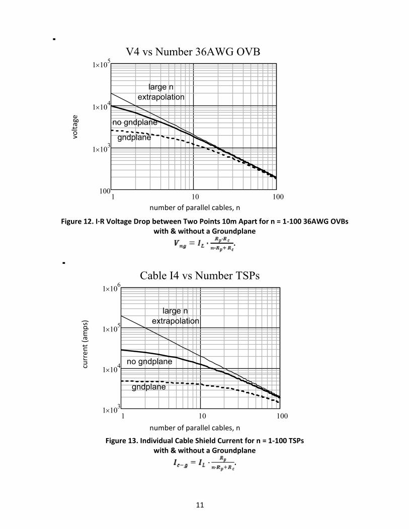
Figure 12 is the total voltage induced end-to-end with only AWG 36 overbraid cables and with andwithout a 15mΩ groundplane. As the number of cables increases, the effect of the groundplanediminishes. The WF4 voltage without the groundplane ranges from 10kV to 200V. With thegroundplane, the WF4 voltage ranges from 2.6kV to 200V. The voltage is dependent on the distancebetween inter-connected boxes. The resistance is proportional to the ratio of length/(width∙thickness).
Figure 13 shows the induced WF4 current on one out of n = 1-100 TSP cables (40mΩ/m), with andwithout the 15mΩ groundplane. Without the groundplane, the individual cable current ranges from20kA to 2kA. With the groundplane, the cable current ranges from 5kA to 1.4kA. The current isindependent of length between inter-connected boxes.
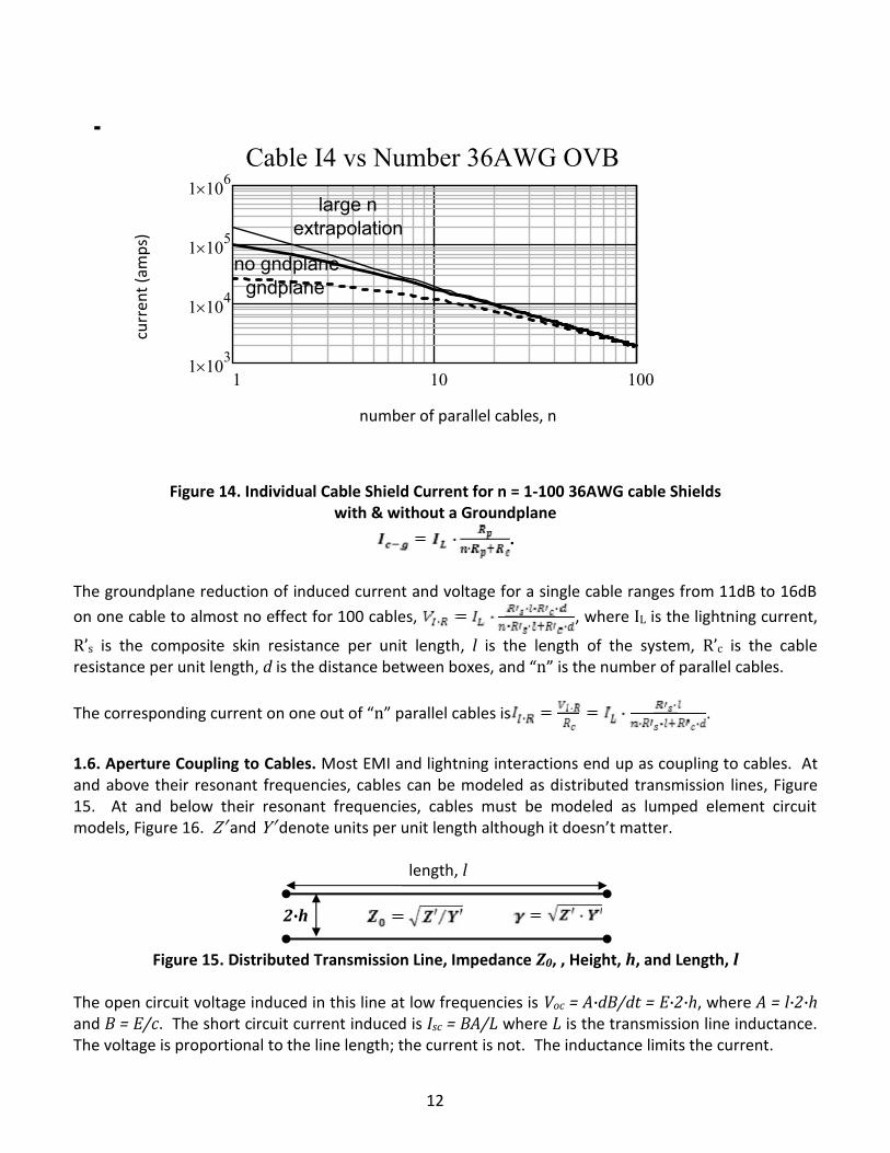
Figure 14 shows the induced WF4 current on one out of n = 1-100 AWG 36 wire braid shielded cables(10mΩ/m), with and without the 15mΩ groundplane. Without the groundplane, the individual cablecurrent ranges from 100kA to 2kA. With the groundplane, the cable current ranges from 28kA to 2kA.The current is independent of length between inter-connected boxes.
number of parallel cables, n
volta
ge
11
1 10 100100
1 103
1 104
1 105
V4 vs Number 36AWG OVB
V4s2 n( )
V4g2 n( )
V4c2 n( )
n
large nextrapolation
no gndplane
gndplane
Figure 12. I·R Voltage Drop between Two Points 10m Apart for n = 1-100 36AWG OVBswith & without a Groundplane
.
1 10 1001 103
1 104
1 105
1 106
Cable I4 vs Number TSPs
I4cs1 n( )
I4cg1 n( )
I4c n( )
n
large nextrapolation
no gndplane
gndplane
Figure 13. Individual Cable Shield Current for n = 1-100 TSPswith & without a Groundplane
.
volta
ge
number of parallel cables, n
number of parallel cables, n
curr
ent (
amps
)
12
1 10 1001 103
1 104
1 105
1 106
Cable I4 vs Number 36AWG OVB
I4cs2 n( )
I4cg2 n( )
I4c n( )
n
large nextrapolation
no gndplanegndplane
Figure 14. Individual Cable Shield Current for n = 1-100 36AWG cable Shieldswith & without a Groundplane
.
The groundplane reduction of induced current and voltage for a single cable ranges from 11dB to 16dB
on one cable to almost no effect for 100 cables, , where IL is the lightning current,R’s is the composite skin resistance per unit length, l is the length of the system, R’c is the cableresistance per unit length, d is the distance between boxes, and “n” is the number of parallel cables.
The corresponding current on one out of “n” parallel cables is .
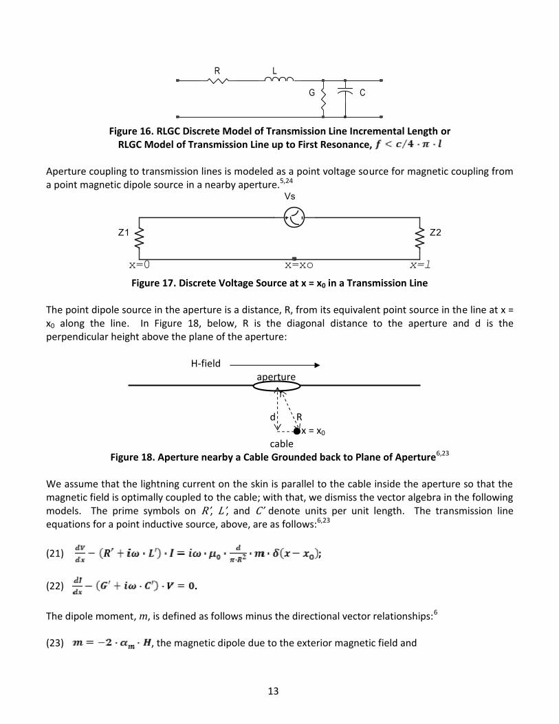
1.6. Aperture Coupling to Cables. Most EMI and lightning interactions end up as coupling to cables. Atand above their resonant frequencies, cables can be modeled as distributed transmission lines, Figure15. At and below their resonant frequencies, cables must be modeled as lumped element circuitmodels, Figure 16. Z′ and Y′ denote units per unit length although it doesn’t matter.
length, l
2∙h
Figure 15. Distributed Transmission Line, Impedance Z0, , Height, h, and Length, l
The open circuit voltage induced in this line at low frequencies is Voc = A∙dB/dt = E∙2∙h, where A = l∙2∙hand B = E/c. The short circuit current induced is Isc = BA/L where L is the transmission line inductance.The voltage is proportional to the line length; the current is not. The inductance limits the current.
curr
ent (
amps
)
number of parallel cables, n
13
C
LR
G
Figure 16. RLGC Discrete Model of Transmission Line Incremental Length orRLGC Model of Transmission Line up to First Resonance,
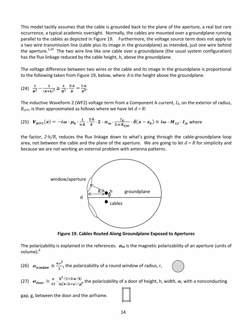
Aperture coupling to transmission lines is modeled as a point voltage source for magnetic coupling froma point magnetic dipole source in a nearby aperture.5,24
Z1 Z2
Vs
x=0 x=xo x=lFigure 17. Discrete Voltage Source at x = x0 in a Transmission Line
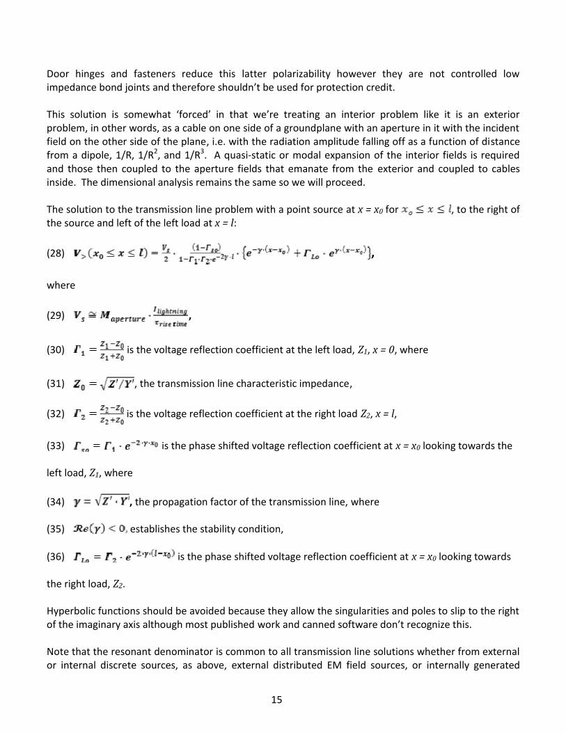
The point dipole source in the aperture is a distance, R, from its equivalent point source in the line at x =x0 along the line. In Figure 18, below, R is the diagonal distance to the aperture and d is theperpendicular height above the plane of the aperture:
H-fieldaperture
d Rx = x0
cableFigure 18. Aperture nearby a Cable Grounded back to Plane of Aperture6,23
We assume that the lightning current on the skin is parallel to the cable inside the aperture so that themagnetic field is optimally coupled to the cable; with that, we dismiss the vector algebra in the followingmodels. The prime symbols on R’, L’, and C’ denote units per unit length. The transmission lineequations for a point inductive source, above, are as follows:6,23
(21) ;
(22) .
The dipole moment, m, is defined as follows minus the directional vector relationships:6
(23) , the magnetic dipole due to the exterior magnetic field and
14
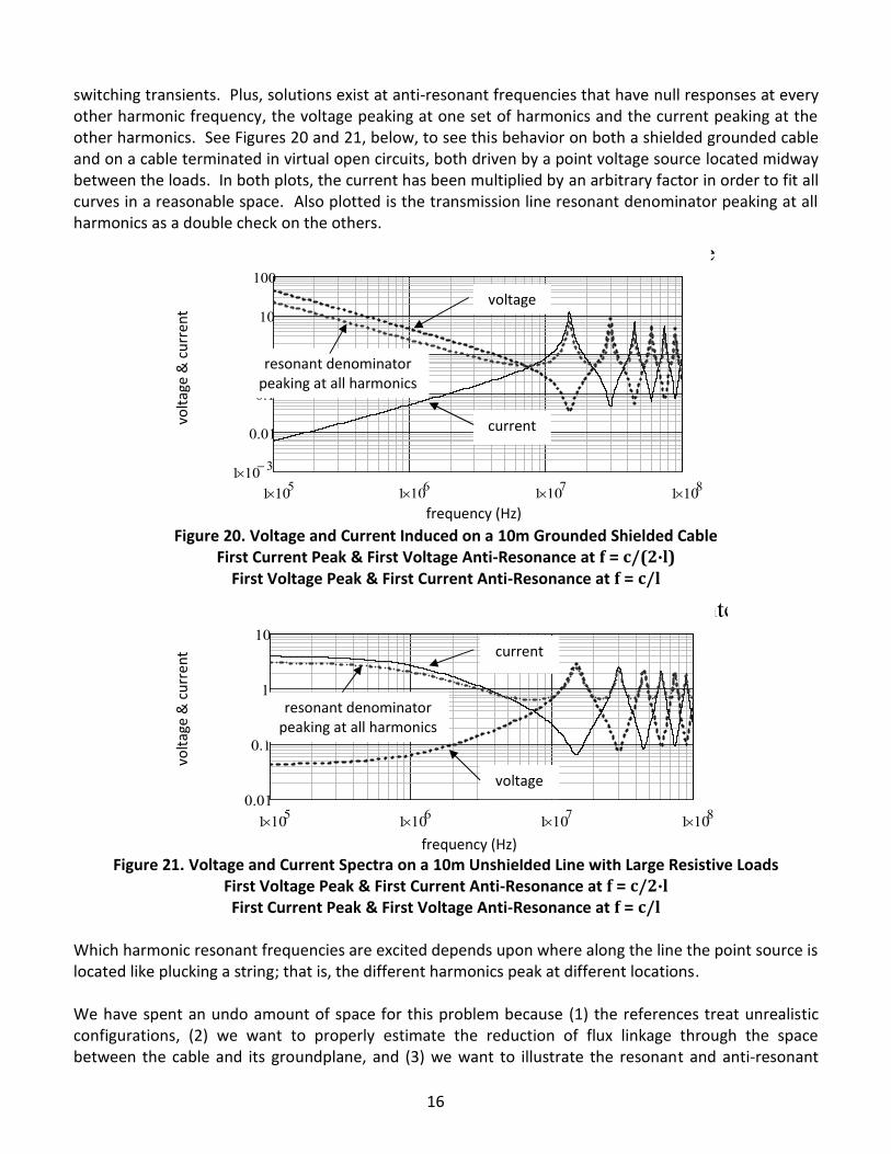
This model tacitly assumes that the cable is grounded back to the plane of the aperture, a real but rareoccurrence, a typical academic oversight. Normally, the cables are mounted over a groundplane runningparallel to the cables as depicted in Figure 19. Furthermore, the voltage source term does not apply toa two wire transmission line (cable plus its image in the groundplane) as intended, just one wire behindthe aperture.5,24 The two wire line like one cable over a groundplane (the usual system configuration)has the flux linkage reduced by the cable height, h, above the groundplane.
The voltage difference between two wires or the cable and its image in the groundplane is proportionalto the following taken from Figure 19, below, where h is the height above the groundplane.
(24) .
The inductive Waveform 2 (WF2) voltage term from a Component A current, IA, on the exterior of radius,Rsyst, is then approximated as follows where we have let d = R:
(25) , where
the factor, 2·h/R, reduces the flux linkage down to what’s going through the cable-groundplane looparea, not between the cable and the plane of the aperture. We are going to let d = R for simplicity andbecause we are not working an external problem with antenna patterns.
window/aperture
R hd
cables
Figure 19. Cables Routed Along Groundplane Exposed to Apertures
The polarizability is explained in the references. αm is the magnetic polarizability of an aperture (units ofvolume):6
(26) , the polarizability of a round window of radius, r,
(27) , the polarizability of a door of height, h, width, w, with a nonconducting
gap, g, between the door and the airframe.
groundplane
15
Door hinges and fasteners reduce this latter polarizability however they are not controlled lowimpedance bond joints and therefore shouldn’t be used for protection credit.
This solution is somewhat ‘forced’ in that we’re treating an interior problem like it is an exteriorproblem, in other words, as a cable on one side of a groundplane with an aperture in it with the incidentfield on the other side of the plane, i.e. with the radiation amplitude falling off as a function of distancefrom a dipole, 1/R, 1/R2, and 1/R3. A quasi-static or modal expansion of the interior fields is requiredand those then coupled to the aperture fields that emanate from the exterior and coupled to cablesinside. The dimensional analysis remains the same so we will proceed.
The solution to the transmission line problem with a point source at x = x0 for , to the right ofthe source and left of the left load at x = l:
(28) ,
where
(29) ,
(30) is the voltage reflection coefficient at the left load, Z1, x = 0, where
(31) , the transmission line characteristic impedance,
(32) is the voltage reflection coefficient at the right load Z2, x = l,
(33) is the phase shifted voltage reflection coefficient at x = x0 looking towards the
left load, Z1, where
(34) , the propagation factor of the transmission line, where
(35) establishes the stability condition,
(36) is the phase shifted voltage reflection coefficient at x = x0 looking towards
the right load, Z2.
Hyperbolic functions should be avoided because they allow the singularities and poles to slip to the rightof the imaginary axis although most published work and canned software don’t recognize this.
Note that the resonant denominator is common to all transmission line solutions whether from externalor internal discrete sources, as above, external distributed EM field sources, or internally generated
16
switching transients. Plus, solutions exist at anti-resonant frequencies that have null responses at everyother harmonic frequency, the voltage peaking at one set of harmonics and the current peaking at theother harmonics. See Figures 20 and 21, below, to see this behavior on both a shielded grounded cableand on a cable terminated in virtual open circuits, both driven by a point voltage source located midwaybetween the loads. In both plots, the current has been multiplied by an arbitrary factor in order to fit allcurves in a reasonable space. Also plotted is the transmission line resonant denominator peaking at allharmonics as a double check on the others.
1 105 1 106 1 107 1 1081 10 3
0.01
0.1
1
10
100Shielded Line Current at Load & Vs at Center
Isw n( ) 100
Vsw n( )
1D n( )
f n( )Figure 20. Voltage and Current Induced on a 10m Grounded Shielded Cable
First Current Peak & First Voltage Anti-Resonance at f = c/(2∙l)First Voltage Peak & First Current Anti-Resonance at f = c/l
1 105 1 106 1 107 1 1080.01
0.1
1
10Unshielded Line V & I at Load & Vs at Center
Isw n( ) 100
Vsw n( )
1D n( )
f n( )Figure 21. Voltage and Current Spectra on a 10m Unshielded Line with Large Resistive Loads
First Voltage Peak & First Current Anti-Resonance at f = c/2∙lFirst Current Peak & First Voltage Anti-Resonance at f = c/l
Which harmonic resonant frequencies are excited depends upon where along the line the point source islocated like plucking a string; that is, the different harmonics peak at different locations.
We have spent an undo amount of space for this problem because (1) the references treat unrealisticconfigurations, (2) we want to properly estimate the reduction of flux linkage through the spacebetween the cable and its groundplane, and (3) we want to illustrate the resonant and anti-resonant
current
current
voltage
voltage
resonant denominatorpeaking at all harmonics
resonant denominatorpeaking at all harmonics
volta
ge &
cur
rent
frequency (Hz)
volta
ge &
cur
rent
frequency (Hz)
17
behavior of transmission lines excited by point sources. The reduction in flux linkage has been modeledfor crosstalk between two cables above a groundplane, below, versus cables dangling in free space butnot for aperture coupling.6
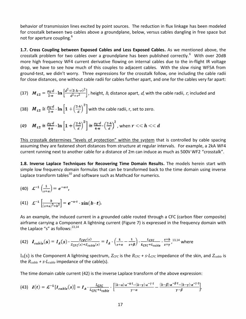
1.7. Cross Coupling between Exposed Cables and Less Exposed Cables. As we mentioned above, thecrosstalk problem for two cables over a groundplane has been published correctly.6 With over 20dBmore high frequency WF4 current derivative flowing on internal cables due to the in-flight IR voltagedrop, we have to see how much of this couples to adjacent cables. With the slow rising WF5A fromground-test, we didn’t worry. Three expressions for the crosstalk follow, one including the cable radiifor close distances, one without cable radii for cables further apart, and one for the cables very far apart:
(37) , height, h, distance apart, d, with the cable radii, r, included and
(38) with the cable radii, r, set to zero.
(49 , when
This crosstalk determines “levels of protection” within the system that is controlled by cable spacingassuming they are fastened short distances from structure at regular intervals. For example, a 2kA WF4current running next to another cable for a distance of 2m can induce as much as 500V WF2 “crosstalk”.
1.8. Inverse Laplace Techniques for Recovering Time Domain Results. The models herein start withsimple low frequency domain formulas that can be transformed back to the time domain using inverseLaplace transform tables10 and software such as Mathcad for numerics.
(40) ,
(41) .
As an example, the induced current in a grounded cable routed through a CFC (carbon fiber composite)airframe carrying a Component A lightning current (Figure 7) is expressed in the frequency domain withthe Laplace “s” as follows:13,14
(42) ,13,14 where
IA(s) is the Component A lightning spectrum, ZCFC is the RCFC + s∙LCFC impedance of the skin, and Zcable isthe Rcable + s∙Lcable impedance of the cable(s).
The time domain cable current (42) is the inverse Laplace transform of the above expression:
(43) ,
18
from a Table of Laplace Transforms.10
The current is the sum of four different time domain exponentials each with a different amplitudedetermined by the different lightning and system parameters, above. The system inverse time constant,γ-1, competes with the lightning rise and fall times for the definition of the induced waveform, aphenomenon unique to the parallel RL branches driven by a current source.13,14
1.9. Cable Shielding. The low frequency transfer impedance of a coaxial shield of length, l, radius, r, andthickness, t, is approximated as follows:6,7
(44) . where Rdc is the DC resistance (5) , above, and
(45) is the diffusion time through the shield wall thickness, t.
We will simplify this to the following so that we can use the Laplace transform tables to obtain ananswer, capturing the low frequency effect of the diffusion time on the rise and fall times of the shieldedtransient but compromising the accuracy of the higher frequency portion which we are not concernedwith anyway at this level of application:
(46) .6
Higher frequency cable shielding includes the transfer inductance, LT, magnetic leakage through themany holes in a braid shield quantified by the optical coverage. The transfer impedance is then definedas follows and an example plot in Figure 22:
(47) .
The last sinx/x term is due to the difference in the velocity of propagation between the external, ve, andinternal, vi, waves where the velocity is inversely proportional to the square root of the dielectricconstants of the two different insulation materials, . It’s a high frequency effect that seldomconcerns lightning shielding. Wire manufacturers use their good insulation around the wires and thecheap stuff for the jacket hence the difference.
The transfer inductance, L’T, can vary over a range of 1pH/m to 1nH/m. It is controlled for the mostpart by specifying the optical coverage of the braid shields, nominally 85% to 95%. Any more and thebraid gets too stiff.
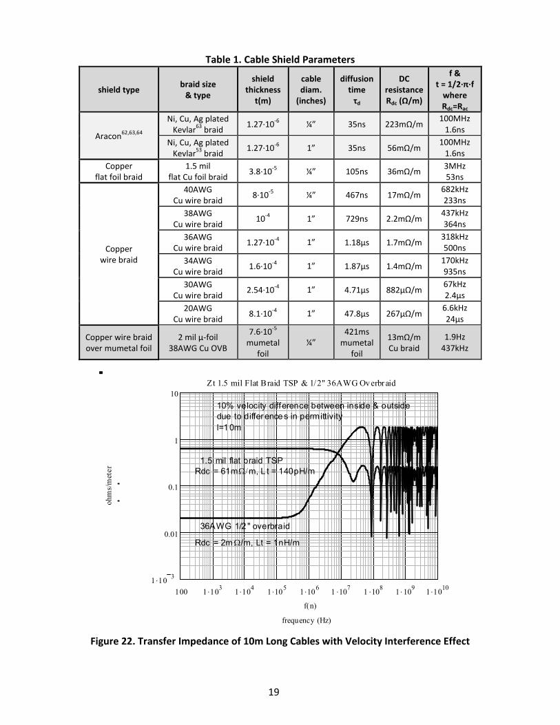
Table 1 summarizes cable shield parameters in several ways for the diverse set of intended readers.
19
Table 1. Cable Shield Parameters
shield typebraid size
& type
shieldthickness
t(m)
cablediam.
(inches)
diffusiontime
τd
DCresistanceRdc (Ω/m)
f &t = 1/2∙π∙f
whereRdc=Rac
Aracon62,63,64
Ni, Cu, Ag platedKevlar63 braid
1.27·10-6 ¼” 35ns 223mΩ/m100MHz
1.6nsNi, Cu, Ag plated
Kevlar53 braid1.27·10-6 1” 35ns 56mΩ/m
100MHz1.6ns
Copperflat foil braid
1.5 milflat Cu foil braid
3.8·10-5 ¼” 105ns 36mΩ/m3MHz53ns
Copperwire braid
40AWGCu wire braid
8·10-5 ¼” 467ns 17mΩ/m682kHz233ns
38AWGCu wire braid
10-4 1” 729ns 2.2mΩ/m437kHz364ns
36AWGCu wire braid
1.27·10-4 1” 1.18μs 1.7mΩ/m318kHz500ns
34AWGCu wire braid
1.6·10-4 1” 1.87μs 1.4mΩ/m170kHz935ns
30AWGCu wire braid
2.54·10-4 1” 4.71μs 882μΩ/m67kHz2.4μs
20AWGCu wire braid
8.1·10-4 1” 47.8μs 267μΩ/m6.6kHz24μs
Copper wire braidover mumetal foil
2 mil μ-foil38AWG Cu OVB
7.6·10-5
mumetalfoil
¼”421ms
mumetalfoil
13mΩ/mCu braid
1.9Hz437kHz
100 1 103 1 104 1 105 1 106 1 107 1 108 1 109 1 10101 10 3
0.01
0.1
1
10Zt 1.5 mil Flat Braid TSP & 1/2" 36AWG Overbr aid
frequency (Hz)
ohm
s/m
eter
Ztint n( )
Zt1int n( )
f n( )
10% velocity difference between inside & outsidedue to difference s in permittivityl=1 0m
1.5 mil flat braid TSPRdc = 61mm, L t = 140pH/m
36AWG 1/2 " overbraid
Rdc = 2m/m, Lt = 1nH/m
Figure 22. Transfer Impedance of 10m Long Cables with Velocity Interference Effect
20
The transfer inductance is important mostly for higher frequency lightning WF3 damped sinusoids. Thehigh frequency velocity interference effect above 10MHz is an EMI issue. For lightning, the DCresistance, Rdc, and diffusion time, τd, are the most important parameters which in turn are functions ofcable length, cable radius, shield thickness, shield conductivity, and shield magnetic permeability.
1.10. Scaling by Geometric, Electrical, and Spectral Parameters. All of the coupling parameters andelectrical system elements are functions of their geometries and distance from the sources of couplingto the induced voltages and currents on the cables.
Examples of scaling:
(a) Aperture mutual coupling is dimensionally proportional to the aperture radius, r cubed, the cableheight above a groundplane, h, and the square of the distance, R, of a cable away from the aperture,and the system radius, Rsyst, at that location i.e. .
(b) Structural and cable resonant frequencies, f, are inversely proportional to the length, l, of both,generally as half wavelengths, i.e. .
(c) Structural resonances, f = ω/2·π, occur between 1MHz and 20MHz, well above the second breakfrequency of the lightning spectrum at βA/2π = 103kHz. When the lightning spectrum drives an RLCresonant circuit, the time domain amplitude is proportional to β/ω3. That is, the higher the resonantfrequency, ω3, because of the smaller lengths, the lower the amplitude of the induced resonanttransient, i.e. the peak WF3 current is proportional to the peak Component A current as follows:
(48) .
This cable inductance is the external inductance because the cable is part of a closed loop circuit ofdifferential, IDM = I1-I2, currents, with length, l, height, h, and radius, r.
(49) .
(d) I·R-drop voltages, , are functions of the following:
(i) distance between interconnected boxes,(ii) aircraft skin resistance, (scales as length/radius x thickness x conductivity)(iii) cable resistance (scales as length/ radius x thickness x conductivity),(iv) groundplane resistance, (scales as length/ width x thickness x conductivity) and(v) number of cables and other conductors parallel to the common mode lightning current throughthe system.
The associated cable currents, , are functions of the same except distance between
boxes. The induced voltage is proportional to length of shielded cables if the cables do not run in astraight line between boxes. This is tacitly included in cable resistance, above, however.
21
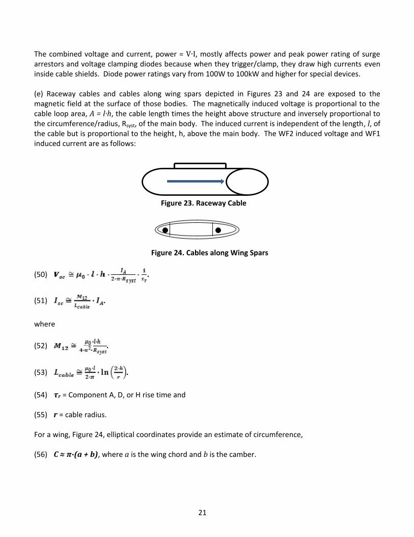
The combined voltage and current, power = V∙I, mostly affects power and peak power rating of surgearrestors and voltage clamping diodes because when they trigger/clamp, they draw high currents eveninside cable shields. Diode power ratings vary from 100W to 100kW and higher for special devices.
(e) Raceway cables and cables along wing spars depicted in Figures 23 and 24 are exposed to themagnetic field at the surface of those bodies. The magnetically induced voltage is proportional to thecable loop area, A = l·h, the cable length times the height above structure and inversely proportional tothe circumference/radius, Rsyst, of the main body. The induced current is independent of the length, l, ofthe cable but is proportional to the height, h, above the main body. The WF2 induced voltage and WF1induced current are as follows:
Figure 23. Raceway Cable
Figure 24. Cables along Wing Spars
(50) .
(51) .
where
(52) .
(53) .
(54) τr = Component A, D, or H rise time and
(55) r = cable radius.
For a wing, Figure 24, elliptical coordinates provide an estimate of circumference,
(56) C ≈ π∙(a + b), where a is the wing chord and b is the camber.
22
2. SAE ARP5412A Indirect Lightning Environments & RTCA/DO-160F Test Environments
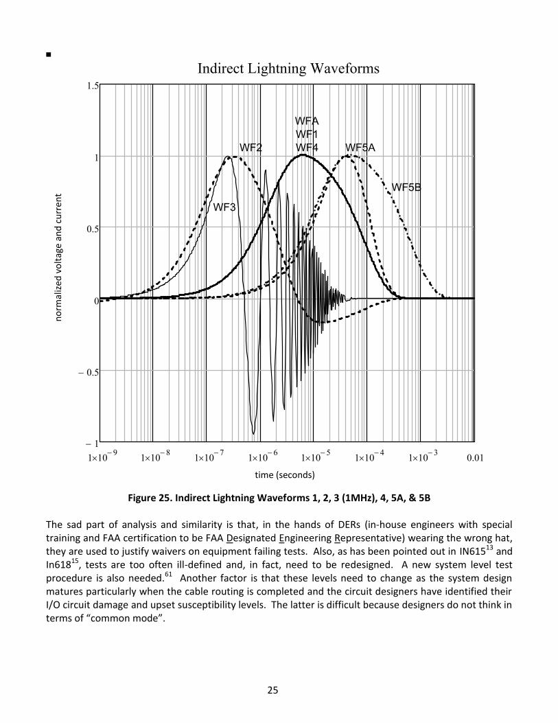
2.1. Lightning Standard Environments. Table 2 is the definition of the indirect lightning waveforms,graphed in Figure 25. Table 3 is the definitions of the thresholds and environment levels based upon thesource of their data. Figure 26 is a definition of safety margins for certification purposes. Tables 4-8 ofindirect lightning to cables and pins for damage by amplitude levels and waveforms from SAEARP5412A2 and RTCA/DO-160F1 Section 22 caused by an 18µs/88µs double exponential Component A200kA negative lightning current2 on the airframe and allocations for functional upset from the multiplestrike 100kA Component D and 10kA Component H. This note does not address the effects of differentlightning strike zones on indirect lightning preferring to assume all parts of the airframe are in Zone 3Current Conduction Zone conducting 200kA Component A.35 The exceptions are components on theskin exposed to any one or all of the different direct multiple and multi-burst strikes or swept strokes inthe different zones. The entries in Tables 3 through 7 are interpreted to be the box design and testlevels although other waveforms and levels are allowed. One purpose of this note is to get rid of thesemisleading “one-size-fits-all” tables and replace them with simple model formulas for scaling the levelsand waveforms by each system’s size, material composition, and cable geometries. Multiple StrokeComponent D and Multiple Burst Component H levels are allegedly only for functional upset howevertheir high frequency content is the same as Component A. The average engineer believes that thesetables apply to all systems and will erroneously choose levels from them without guidance to thecontrary. Companies with electromagnetic and lightning expertise develop their own tables tailored totheir specific aircraft.29,38 This note intends for everyone to do so with the tools provided herein.
Before we tabulate the indirect lightning environments in the standards, let’s introduce the standardizedexternal strike components and the resulting internal indirect lightning.
2.1.1. Direct Strike Components used to Define Indirect Transients. The external direct lightning strikesthemselves are given alphabetic designations, WFA-WFH although indirect lightning is derived only fromComponents A, D, and H, below.2
(57) , the single stroke 200kA Component A;
(58) , Multiple Stroke 100kA Component D followed by 13
more, 50kA D/2, at half this amplitude, 10ms to 200ms apart, all within 1.5 seconds;
(59) , Multi-Burst 10kA Component H, three bursts of twenty
transients each, 50µs to 100µs between transients, 30ms to 300ms between bursts, all within 620ms.
Components D and H have been relegated to functional upset threats while Component A has beenrelegated to a damage threat. These three exterior strike Components A, D, and H have about the samedI/dt and the same spectral content, , above 1MHz meaning that they will excite the same WF2 andWF3 indirect transients. That does not relegate them to only “functional upset” as in the standards,especially when their levels in Tables 5, 6, and 7 meet or exceed the “damage levels” in Tables 3 and 4.
23
2.1.2. Indirect Lightning Waveforms’ Definitions. Let’s define the indirect waveforms and the rationalefor their designations, remembering that these all have been derived from present-day system levelground tests.13
Waveform 1 (WF1) is induced through aperture or inductive coupling and is the same as the lightningComponent A waveform; this characteristically appears as a current on a shielded cables;
(60)
Waveform 2 (WF2) is the time derivative of lightning Component A or WF4; it appears as a voltageinduced through inductive coupling from the lightning current Component A on the skin;
(61)
There also exist undefined versions of this for Components D and H although the peak WF2 voltage isthe same for all three, A, D, and H.
Waveform 3 (WF3) is a resonant damped sinusoid whose amplitude and frequency depend upon thelength of the resonating element, either (a) the airframe as a whole or (b) individual cables;
(62) .
Waveform 4 (WF4) is induced through the resistive voltage drop through a CFC (carbon fiber composite)skin. V = I·R, and is the same as that of the lightning current Component A (and Waveform 1);
(63)
Waveform 5A (WF5A) is the current induced on cable shields grounded at both ends in a CFC airframeduring ground-test with a nearby return current, shown below as the inverse Laplace transform of thefrequency domain model; in-flight, with no return current, this cable current is WF4;13
(64)
Waveform 5B (WF5B)is the voltage induced on cables diffused through the transfer impedance of analuminum skinned airframe; it is small, long, and usually ignored;
(65)
Waveform 4 is erroneously attributed also to lightning Component D (See Table 5, above.) althoughthere are circumstances where that confusion is not surprising. (Discussed in Section 10.)
Waveform 6H (WF6H) is the current induced on cables from the multi-burst lightning Component H;
(66)
24
How WF6H got onto cables in SAE ARP5412A for Component H and a corresponding WF6D didn’t make itfor Component D is one of the inconsistencies in the standards; it’s because WF4 is used for theComponent D strikes. Components D and H will not usually strike the same location on the aircraftunless it’s moving very slowly therefore some of those strikes will diffuse through the CFC skin with acorresponding increase in rise time instead of striking on a spot connected to the interior cables and/orgroundplane.
Table 2. Standardized Indirect Lightning Waveforms1,2
Extracted from Table 9 in SAE ARP5412A
• Component A and Waveforms 1 and 4 are the same 1.5µs/88µs double exponential with a
x1.094 multiplier, i.e. peaks at 200kA.
• Waveform 2 is the derivative of Waveform A, 1, and 4 with a x1.00 multiplier. (See note below.)
• Waveform 3 is a damped sinusoid waveform at 1 and 10MHZ with a damping Q-value of 9-37
with a x1.059 multiplier.
• Waveform 5 consists of two waveforms:
Waveform 5A is a 23µs/79µs double exponential with a x2.334 multiplier.
Waveform 5B is a 12.5µs/631µs double exponential with a x1.104 multiplier.
• Waveform 6D doesn’t exist having been replaced with WF4.
• Waveform 6H is a 5.2ns/5.3µs double exponential associated with Component H.
Note: WF2 doesn’t graph like the derivative definition, above, but does graph nicely as the following:
(67) .
2.1.3. Tables of Allocated Indirect Lightning Waveforms and Levels.
The indirect lightning environments that are provided by SAE ARP5412A and RTCA/DO-160F aretabulated below in Tables 3-7 as they appear in those standards. These are intended to be both designand test levels. Other waveforms derived by the various programs are designated Waveform Z.Rationale for the different levels follows the tables. Definitions of the transient level acronyms follownext along with their intended use in estimating safety margins of the equipment in the system.
Table 2, below, appears to be an over-laborious set of acronyms simply to ensure that inducedtransients do not exceed box failure thresholds.1,2,5 However, ATL has been broken into severalcategories depending upon the origin of the data, in agreement with FAA AC 20-136A;5 for example (a)ATLt, the intended extrapolated system test data and box test data, (b) ATLa, system modeling andanalyses, and (c) ATLs, similarity through scaling by geometry and electrical parameters.
25
1 10 9 1 10 8 1 10 7 1 10 6 1 10 5 1 10 4 1 10 3 0.011
0.5
0
0.5
1
1.5Indirect Lightning Waveforms
IA n( )
V3 n( )
I5A n( )
I5B n( )
V2 n( )
t n( )
WFAWF1WF4WF2 WF5A
WF5B
WF3
Figure 25. Indirect Lightning Waveforms 1, 2, 3 (1MHz), 4, 5A, & 5B
The sad part of analysis and similarity is that, in the hands of DERs (in-house engineers with specialtraining and FAA certification to be FAA Designated Engineering Representative) wearing the wrong hat,they are used to justify waivers on equipment failing tests. Also, as has been pointed out in IN61513 andIn61815, tests are too often ill-defined and, in fact, need to be redesigned. A new system level testprocedure is also needed.61 Another factor is that these levels need to change as the system designmatures particularly when the cable routing is completed and the circuit designers have identified theirI/O circuit damage and upset susceptibility levels. The latter is difficult because designers do not think interms of “common mode”.
time (seconds)
norm
aliz
ed v
olta
ge a
nd c
urre
nt
26
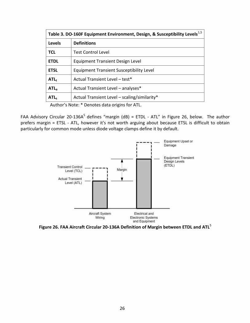
Table 3. DO-160F Equipment Environment, Design, & Susceptibility Levels1,5
Levels Definitions
TCL Test Control Level
ETDL Equipment Transient Design Level
ETSL Equipment Transient Susceptibility Level
ATLt Actual Transient Level – test*
ATLa Actual Transient Level – analyses*
ATLs Actual Transient Level – scaling/similarity*
Author’s Note: * Denotes data origins for ATL.
FAA Advisory Circular 20-136A5 defines “margin (dB) = ETDL - ATL” in Figure 26, below. The authorprefers margin = ETSL - ATL, however it's not worth arguing about because ETSL is difficult to obtainparticularly for common mode unless diode voltage clamps define it by default.
Figure 26. FAA Aircraft Circular 20-136A Definition of Margin between ETDL and ATL5
27
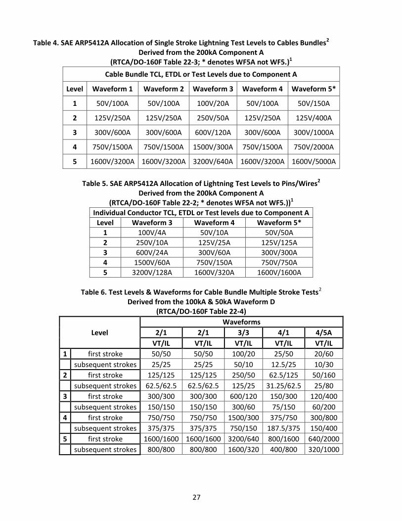
Table 4. SAE ARP5412A Allocation of Single Stroke Lightning Test Levels to Cables Bundles2
Derived from the 200kA Component A(RTCA/DO-160F Table 22-3; * denotes WF5A not WF5.)1
Cable Bundle TCL, ETDL or Test Levels due to Component A
Level Waveform 1 Waveform 2 Waveform 3 Waveform 4 Waveform 5*
1 50V/100A 50V/100A 100V/20A 50V/100A 50V/150A
2 125V/250A 125V/250A 250V/50A 125V/250A 125V/400A
3 300V/600A 300V/600A 600V/120A 300V/600A 300V/1000A
4 750V/1500A 750V/1500A 1500V/300A 750V/1500A 750V/2000A
5 1600V/3200A 1600V/3200A 3200V/640A 1600V/3200A 1600V/5000A
Table 5. SAE ARP5412A Allocation of Lightning Test Levels to Pins/Wires2
Derived from the 200kA Component A(RTCA/DO-160F Table 22-2; * denotes WF5A not WF5.))1
Individual Conductor TCL, ETDL or Test levels due to Component ALevel Waveform 3 Waveform 4 Waveform 5*
1 100V/4A 50V/10A 50V/50A2 250V/10A 125V/25A 125V/125A3 600V/24A 300V/60A 300V/300A4 1500V/60A 750V/150A 750V/750A5 3200V/128A 1600V/320A 1600V/1600A
Table 6. Test Levels & Waveforms for Cable Bundle Multiple Stroke Tests2
Derived from the 100kA & 50kA Waveform D(RTCA/DO-160F Table 22-4)
LevelWaveforms
2/1 2/1 3/3 4/1 4/5AVT/IL VT/IL VT/IL VT/IL VT/IL
1 first stroke 50/50 50/50 100/20 25/50 20/60subsequent strokes 25/25 25/25 50/10 12.5/25 10/30
2 first stroke 125/125 125/125 250/50 62.5/125 50/160subsequent strokes 62.5/62.5 62.5/62.5 125/25 31.25/62.5 25/80
3 first stroke 300/300 300/300 600/120 150/300 120/400subsequent strokes 150/150 150/150 300/60 75/150 60/200
4 first stroke 750/750 750/750 1500/300 375/750 300/800subsequent strokes 375/375 375/375 750/150 187.5/375 150/400
5 first stroke 1600/1600 1600/1600 3200/640 800/1600 640/2000subsequent strokes 800/800 800/800 1600/320 400/800 320/1000
28
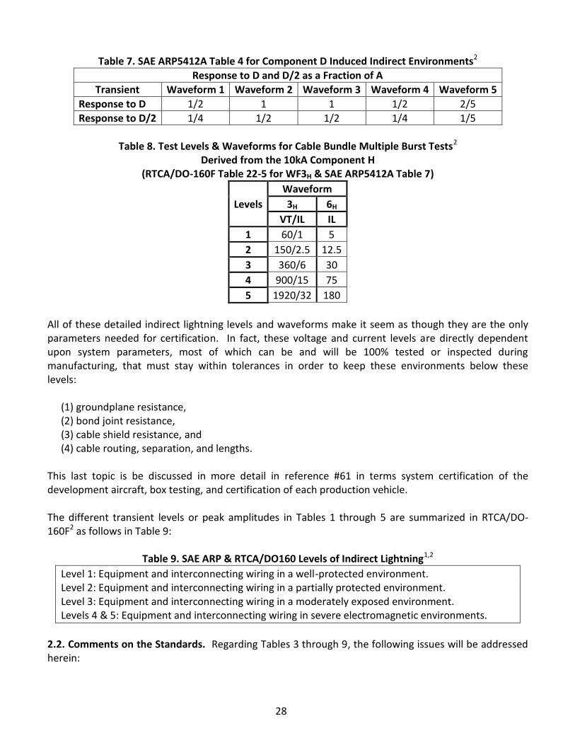
Table 7. SAE ARP5412A Table 4 for Component D Induced Indirect Environments2
Response to D and D/2 as a Fraction of ATransient Waveform 1 Waveform 2 Waveform 3 Waveform 4 Waveform 5
Response to D 1/2 1 1 1/2 2/5Response to D/2 1/4 1/2 1/2 1/4 1/5
Table 8. Test Levels & Waveforms for Cable Bundle Multiple Burst Tests2
Derived from the 10kA Component H(RTCA/DO-160F Table 22-5 for WF3H & SAE ARP5412A Table 7)
LevelsWaveform3H 6H
VT/IL IL1 60/1 52 150/2.5 12.53 360/6 304 900/15 755 1920/32 180
All of these detailed indirect lightning levels and waveforms make it seem as though they are the onlyparameters needed for certification. In fact, these voltage and current levels are directly dependentupon system parameters, most of which can be and will be 100% tested or inspected duringmanufacturing, that must stay within tolerances in order to keep these environments below theselevels:
(1) groundplane resistance,(2) bond joint resistance,(3) cable shield resistance, and(4) cable routing, separation, and lengths.
This last topic is be discussed in more detail in reference #61 in terms system certification of thedevelopment aircraft, box testing, and certification of each production vehicle.
The different transient levels or peak amplitudes in Tables 1 through 5 are summarized in RTCA/DO-160F2 as follows in Table 9:
Table 9. SAE ARP & RTCA/DO160 Levels of Indirect Lightning1,2
Level 1: Equipment and interconnecting wiring in a well-protected environment.Level 2: Equipment and interconnecting wiring in a partially protected environment.Level 3: Equipment and interconnecting wiring in a moderately exposed environment.Levels 4 & 5: Equipment and interconnecting wiring in severe electromagnetic environments.
2.2. Comments on the Standards. Regarding Tables 3 through 9, the following issues will be addressedherein:
29
The term “protected environment” is not defined but it is an opinion about relative levels ofshielding of fields throughout the airframes.20 Since most EEs believe that a tin can full of holespenetrated by ungrounded cables is a shielded enclosure, they will inevitably chooseoveroptimistically low levels. (See Section 5.) This note will redefine these levels and the notionof “protected environment”, develop algorithms for scaling induced environments to match thesystem with box and cable locations, add one or two more levels to capture the very high levelsavoided in these tables, and provide design guidelines for achieving desired levels.
Except for a handful of military aircraft, there are no “shielded” areas in any airframe. There are,however, cables more exposed to intense environments than others that depend upon theirrouting and geometry. Mutual coupling between the more exposed cables and the less exposedcables is then the real basis for “levels of protection” herein. Shielded boxes and cables are theonly reliable and maintainable shielding in most airframes. This note will discuss how to allocatecable shielding.
Levels 1-5 allegedly range from well protected to least protected, a total range of about x32 or30dB. Note, however, the difference between each level is about 7-8dB. Measurement accuracyand repeatability are rarely that good.21 Protection cannot be obtained in such small incrementsexcept when using two layers instead of one layer of cable shield, the “protection” improves by6dB. These levels imply different degrees of shielding from the airframes where shielding is notdesigned, controlled, or maintained and will vary an order of magnitude within such airframes aswell as between airframes. Assumptions about these levels, how to determine them20,21, andwhat they mean have been a misconception across the whole spectrum of EMI and lightningengineering for decades, promoted by those least qualified to address the issue. “Protection” isachieved by (1) cable routing, (2) cable shielding, and (3) circuit protection. See section 5 for amore detailed diatribe.
WF5A cable current from ground-tests is hereby changed to WF4 for in-flight.13
The WF4 I∙R voltage is proportional to the distance between boxes in the lightning current path.The corresponding WF4 cable current is relatively independent of the length between boxes.13
Scaling the I∙R-drop cable current the same as the I∙R-drop voltage is wrong.
Voltages induced inside the cable shields with WF5A, now WF4, currents are proportional to cablelengths, not box distances. This may seem to be a trivial issue however it dictates the ratings ofsurge arrestors placed on the effected lines. See section 13.
The Table 3 Level 5 WF4 voltage and WF5A, now WF4, current are presumably inside a compositefuselage during a ground-test with a 15mΩ low inductance groundplane, i.e. wall-to-wall & nose-to-tail and yet it is still 3x too small for a 78729,38. The table is corrected herein in that WF4 voltagein an in-flight composite airframe is associated with WF4 current on the cables and the voltage isscaled by system and cable lengths.13
Allocating 100V to 3.2kV for functional upset in the standards is akin to allocating a steam roller torepel fleas on a dog. Protection against functional upset is more of a software and fail-safearchitecture issue, anyway.
30
Missing are higher levels in locations without low resistance and low inductance groundplaneswhere voltages can reach 10-20kV for WF2 & 4. The NASA ORION CFC-skinned 100mΩ LaunchAbort System (LAS) had WF4 voltage levels approaching 13kV due to a 200kA strike because of thesmaller diameter and no groundplane.
Waveform 4 and 5A will not exist in-flight when struck by Waveform D lightning transients.Waveform D will appear as an I·R-voltage drop and as a subsequent cable current. Waveform 3will appear as an external resonance or as cable resonances and be the same as Component A.
Table 6 properly connects the correct WF4 voltage and WF5A (now WF4) current waveforms notdone in Tables 4 and 5. However, all of the tables on this IR-drop phenomenon miss the fact thatas WF4 voltage decreases with decreasing distance between boxes along the lightning path, WF5A(now WF4) current remains the same. (This was observed in the Beech Starship during testing atLTI in 1984 and agrees with simple theory.) However, for shielded cables, the induced voltageinside the shields in-flight is proportional to the cable length between boxes and is close to aWF5A waveform (now WF4), the same as on the shield.13,14 IN61815 recommends ground injectiontesting with the “shield disconnect method” using a WF4 voltage because box testing by injectingwith the shields in place will never result in the same waveform induced inside the shields as willbe in-flight. (This is observed in Note 3 of Table 22-3 in DO-160F but promptly ignored.)
Tables 4-8 should have the same WF2 and WF3 peak voltages because the time derivatives of allthree are the same (WF2 ≈ dI/dt) and the spectral content is the same above 2MHz (WF3 isproportional to the lightning components’ spectra above 2MHz)
Tables 4-8 should have WF1 currents, WF4 I∙R-drop voltages, and WF4 I∙R-drop cable currentsproportional to the peak values of their respective external strike Components A, D, and H withwaveforms the same as the external components, say WF6D and WF6H.
Missing is the fact that normal copper cable shields cannot attenuate the low frequency WF4 orWF5 currents.13,14,15 Copper shielding must be at least as thick as a seldom used 30AWG wirebraid or conduit or include a new copper and mumetal cable shield.13,14 See Table 1. Even withextreme shielding, special circuit isolation and voltage limiting is required to mitigate the effects ofthe extreme I∙R-drop environments. See Section 13. Even with extreme shielding and special I/Ocircuit designs, functional upset protection needs special error correcting software orcircumvention techniques so as to prevent unsafe commands from automated flight electronics; towit, the lightning environments are so high that they cannot be reduced to below all susceptibilitythreshold levels by shielding alone. The predominate mode of indirect lightning the cables, wires,and boxes will experience will be the I∙R-drop voltage in the inner most shields. That is whydesigning proper ground injection tests is so important in IN61815. As an example, an ARINC 429vendor, Holt60, feels obliged to allocate pin injection to WF3, WF4, and WF5A, the easiest test topass, even though in-flight all three will appear as I∙R-drops in the innermost cable shield.Message? The tables allow vendors to choose the easiest environments and tests regardless ofthe physics.
31
Missing is any scaling of levels by system size, aperture size and distance to cables, and cablegeometry. See all subsequent sections to see the geometric dependence of the allocatedwaveforms, frequencies, and levels/amplitudes.
Missing is scaling of resonant WF3 amplitudes & frequencies by system length and cablegeometry.
Missing is any algorithm to establish any level in any system, the subject of this note. Mostdesigners believe that Tables 2 through 6 are the extent of their choices. SAE ARP5415A does littleto clarify the issues. The result is a tragicomedy.
This note addresses these issues by developing simple formulas for estimating lightning inducedtransients at the beginning of programs without knowing details about the system. Managers ofprograms that develop composite systems are extremely weight conscious, therefore the lightningengineer must obtain reasonable early results in order to be allocated the weight and space necessaryfor lightning protection. The method is not precise but does allow reasonable estimates for early designallocations. Adjustments can be made to the allocations as design details become available, e.g. boxlocations, cable routing, cable lengths, and circuit susceptibility levels.
Warning: The radial distribution of lightning around the skin is unknown except in the present low levelsystem level lightning ground-test. There the system is made to be the inner conductor of a coaxial testfixture and have a relatively uniform current distribution. Assuming the current to be uniform aroundthe skin is then forcing the allocations to be such as to pass the extrapolated low level test. Nonuniformdistributions can be treated with more sophisticated models, albeit later in a program, and by addingmargins to these allocations. Nonuniform distributions often result in physical damage or degradationsuch as holes in radomes, ailerons being damaged, antennas blown off, and even flight control cableswelded to a rib, based upon past experience. An example of nonuniform currents is the phenomenon ofswept stroke lightning that will move from one attachment point to another from the first attachmenttowards the tail as the vehicle moves through the lightning stroke that remains more or less stationaryin the atmosphere depending upon the speed of the vehicle.35
In reality, at the lowest levels, the allocated voltages are dictated by I/O circuit susceptibilities, ETSL,which in turn define the allocated groundplane, cable and wire shielding, and circuit protection. Inmodern systems with sensitive low voltage electronics, only primary power is unshielded. Everythingelse has at least shielded twisted pair (TSP) level of shielding with 20-70mΩ/m low frequency transferimpedance. The shielding is therefore designed against the allocated shield current and the allowedinduced voltage, with cable length and connector shielding included.
3. Comparisons, WF4 & WF5A in SAE ARP5412A vs. Present In-Flight Results
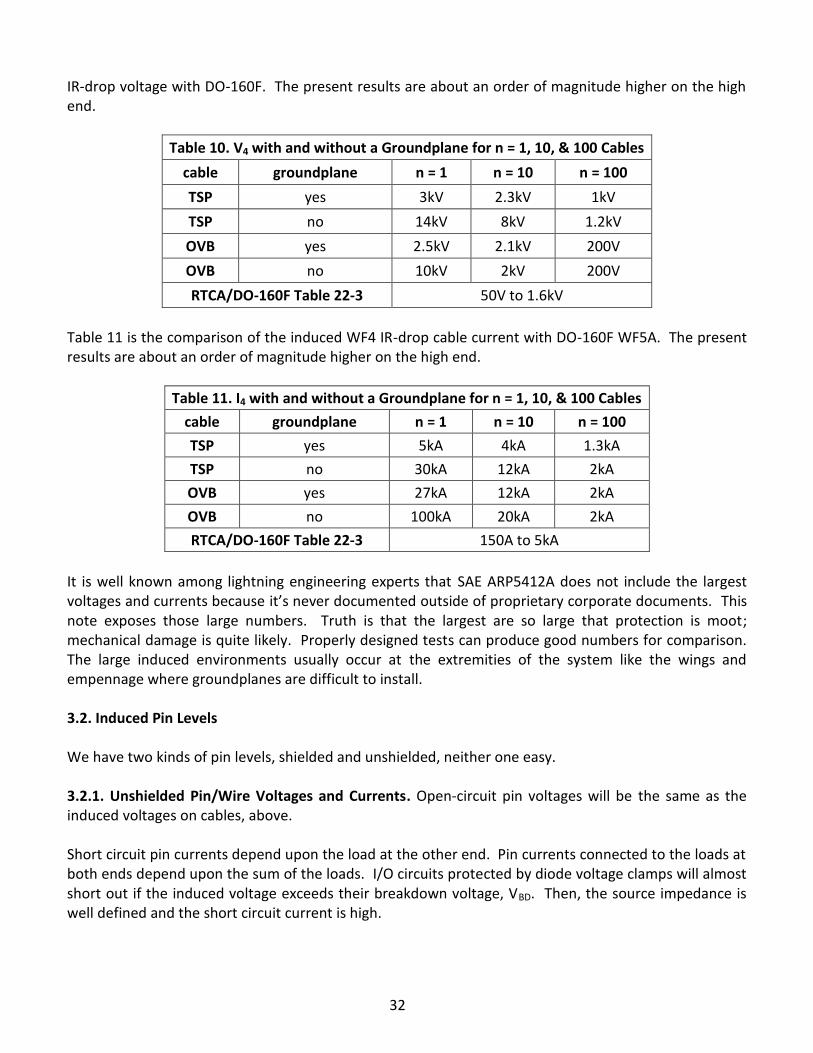
Let’s compare these numbers against those for cable bundles in SAE ARP5412 and DO-160 although nocable lengths or numbers are mentioned in those documents:
3.1. IR-Drop WF4 Voltage & WF4 Cable Current. The following Tables 10 and 11 summarize the abovegraphical results for n = 1, 10, and 100 10m long cables, Figures 11-14. Tables 19-23 in Section 12include the length of cables, also. They show a comparison the maximum and minimum induced WF4
32
IR-drop voltage with DO-160F. The present results are about an order of magnitude higher on the highend.
Table 10. V4 with and without a Groundplane for n = 1, 10, & 100 Cables
cable groundplane n = 1 n = 10 n = 100
TSP yes 3kV 2.3kV 1kV
TSP no 14kV 8kV 1.2kV
OVB yes 2.5kV 2.1kV 200V
OVB no 10kV 2kV 200V
RTCA/DO-160F Table 22-3 50V to 1.6kV
Table 11 is the comparison of the induced WF4 IR-drop cable current with DO-160F WF5A. The presentresults are about an order of magnitude higher on the high end.
Table 11. I4 with and without a Groundplane for n = 1, 10, & 100 Cables
cable groundplane n = 1 n = 10 n = 100
TSP yes 5kA 4kA 1.3kA
TSP no 30kA 12kA 2kA
OVB yes 27kA 12kA 2kA
OVB no 100kA 20kA 2kA
RTCA/DO-160F Table 22-3 150A to 5kA
It is well known among lightning engineering experts that SAE ARP5412A does not include the largestvoltages and currents because it’s never documented outside of proprietary corporate documents. Thisnote exposes those large numbers. Truth is that the largest are so large that protection is moot;mechanical damage is quite likely. Properly designed tests can produce good numbers for comparison.The large induced environments usually occur at the extremities of the system like the wings andempennage where groundplanes are difficult to install.
3.2. Induced Pin Levels
We have two kinds of pin levels, shielded and unshielded, neither one easy.
3.2.1. Unshielded Pin/Wire Voltages and Currents. Open-circuit pin voltages will be the same as theinduced voltages on cables, above.
Short circuit pin currents depend upon the load at the other end. Pin currents connected to the loads atboth ends depend upon the sum of the loads. I/O circuits protected by diode voltage clamps will almostshort out if the induced voltage exceeds their breakdown voltage, VBD. Then, the source impedance iswell defined and the short circuit current is high.
33
Summarizing, pin voltages should be the same as the cable voltages. Pin currents are any one’s guesshowever we should specify short circuit current for power calculations and ratings on surge suppressiondevices. Ideally, the lightning engineer, if he had the time and skills, should give each designer aThevinin equivalent lightning source circuit for each of the designers’ I/O circuits.
3.2.2. Shielded Pin/Wire Voltages and Currents. Shielded pin voltages depend upon (1) thegroundplane resistance, if there is one, (2) the shield length, (3) the shield’s DC resistance, and (4) theshield’s diffusion time. Because indirect lightning is such a low frequency phenomenon, the shieldvoltage will be the Ishld∙Rdc∙l = I∙R-drop in the shield, not the iω∙LT∙lshld voltage in series within theshielded wires.
Bottom line: Shielding the new in flight WF4 cable current is just as near impossible as the WF5Acurrent. Also, the induced voltage is larger, above, because the induced WF4 current on the shield islarger than the old WF5A.
3.3. Waveform 3 Resonant Damped Sinusoid Excitations
Two facts up front, (1) the WF3 frequency is f3 = c/2l, where l is the length of the system and the cablesand (2) the amplitude/level of WF3 is proportional to the length (inversely proportional to thefrequency).
3.3.1. Sources of WF3
WF3 transients have two sources, (1) the resonant airframe and (2) resonant cables. The WF3 airframeresonance is pronounced on aluminum skinned systems but damped far more on CFC skinned systems.The Components A, D, and H external currents will induce the same WF3 resonant currents. The largestWF3 cable currents since IN61413 are those excited on cables with WF4 currents on them. Those, likethe external WF3 currents, will have peak values β/ω3 less than the WF4 currents, where β = 1/(1.5µsrise time) of the WF4 currents.
3.3.2. Waveform 3 Comparisons
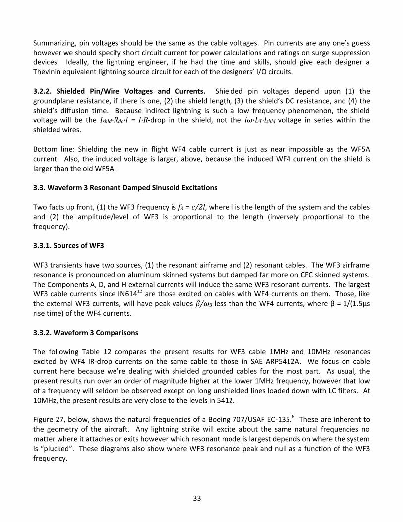
The following Table 12 compares the present results for WF3 cable 1MHz and 10MHz resonancesexcited by WF4 IR-drop currents on the same cable to those in SAE ARP5412A. We focus on cablecurrent here because we’re dealing with shielded grounded cables for the most part. As usual, thepresent results run over an order of magnitude higher at the lower 1MHz frequency, however that lowof a frequency will seldom be observed except on long unshielded lines loaded down with LC filters. At10MHz, the present results are very close to the levels in 5412.
Figure 27, below, shows the natural frequencies of a Boeing 707/USAF EC-135.6 These are inherent tothe geometry of the aircraft. Any lightning strike will excite about the same natural frequencies nomatter where it attaches or exits however which resonant mode is largest depends on where the systemis “plucked”. These diagrams also show where WF3 resonance peak and null as a function of the WF3frequency.
34
Table 12. Comparison of Max Min 5412A WF3 to Present Results
5412A WF31MHz WF3
without/withgndplane
10MHz WF3without/with
gndplane
Level 5412 present present
1 20A 200A/130A 20A/13A
5 640A 10kA/2.7kA 1kA/270A
Figure 27. Natural Resonant Frequencies of a Boeing 707/ USAF EC-1356
4. Shielded versus Unshielded Wires in Composite Airframes
Aircraft usually do not shield power wires and usually use chassis/structure/groundplane for the powerreturn connection. Such wires running any distance will have surge arrestors at both ends large enoughto clamp the WF4 voltage and conduct the maximum WF4 current. Such a wire or set of wires willtherefore respond almost the same as shielded cables grounded at both ends because when the surgearrestors conduct, the wires are effectively grounded into structure. In a composite business aircraft,such surge arrestors have to be rated for 12kVA.
5. Perceptions of Shielding Effectiveness of Unshielded Enclosures
This section addresses the issue of shielding of electromagnetic fields by airframes not designed to do soand the wrong-headed test technique used to obtain such shielding data.
35
The average EMC engineer believes that a tin can full of holes is a shielded enclosure and has the "data"to show it!? Boeing tried to turn one of those tin cans (commercial Boeing 747-100) into a shieldedenclosure at a cost of millions and barely got 25dB. The Navy had the same luck (Lockheed Martin C-130). Of course, that 25dB was REAL – EMP hardened USAF E4-B and USN TACAMO, with every hole andpenetration shielded, filtered, and/or bonded/grounded. The belief that such levels can be achievedwithout protection is horribly wrong-headed. Even worse is the belief that such field data has anybearing on induced transients on cables running through those areas.
The underlying point is that shielding data is always acquired with the wrong test techniques, usuallyresults in 20-30dB of fictitious shielding effectiveness, and is therefore very popular. Bad test data livesforever. This concept is promoted by those least qualified to do so.
The “wrong test technique” is the use of traveling wave antennas (log periodic and horn antennas)inside metal enclosures like an aircraft fuselage where the EM environment is predominately standingwaves. Explaining this error to the uninformed is fruitless. The measurements are always low with nocorrection factor(s) hence very popular. A strong argument against using any such shielding values isthat they are totally uncontrolled, never maintained, and the variation system to system is neverchecked. The costs to do so are exorbitant.
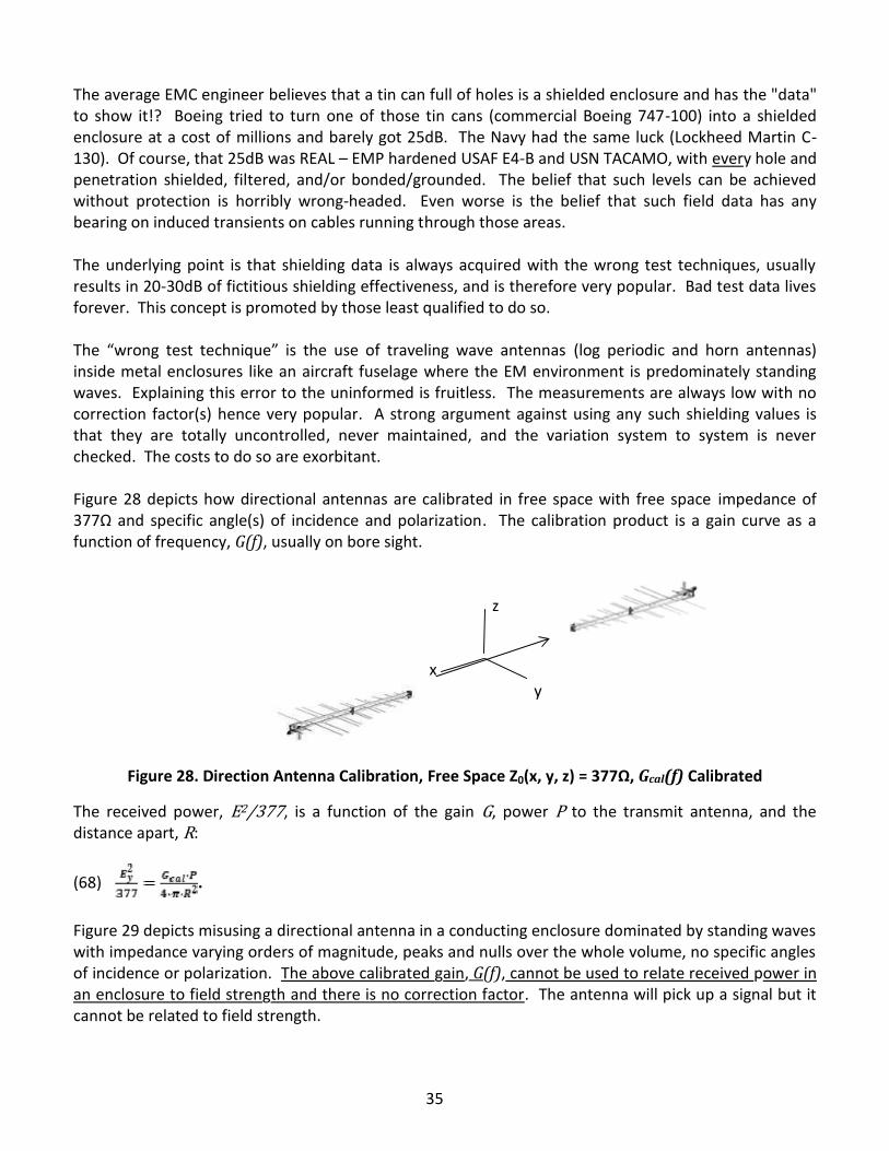
Figure 28 depicts how directional antennas are calibrated in free space with free space impedance of377Ω and specific angle(s) of incidence and polarization. The calibration product is a gain curve as afunction of frequency, G(f), usually on bore sight.
z
xy
Figure 28. Direction Antenna Calibration, Free Space Z0(x, y, z) = 377Ω, Gcal(f) Calibrated
The received power, E2/377, is a function of the gain G, power P to the transmit antenna, and thedistance apart, R:
(68) .
Figure 29 depicts misusing a directional antenna in a conducting enclosure dominated by standing waveswith impedance varying orders of magnitude, peaks and nulls over the whole volume, no specific anglesof incidence or polarization. The above calibrated gain, G(f), cannot be used to relate received power inan enclosure to field strength and there is no correction factor. The antenna will pick up a signal but itcannot be related to field strength.
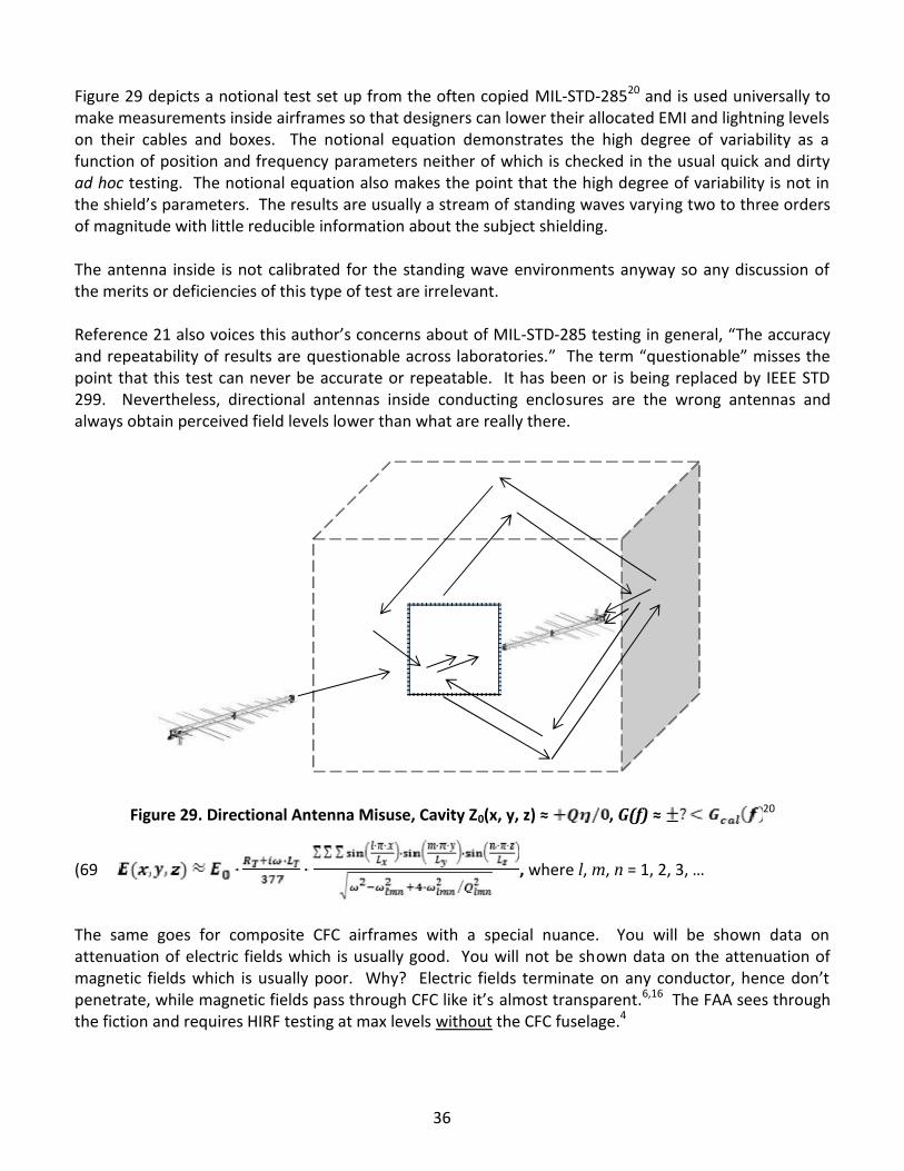
36
Figure 29 depicts a notional test set up from the often copied MIL-STD-28520 and is used universally tomake measurements inside airframes so that designers can lower their allocated EMI and lightning levelson their cables and boxes. The notional equation demonstrates the high degree of variability as afunction of position and frequency parameters neither of which is checked in the usual quick and dirtyad hoc testing. The notional equation also makes the point that the high degree of variability is not inthe shield’s parameters. The results are usually a stream of standing waves varying two to three ordersof magnitude with little reducible information about the subject shielding.
The antenna inside is not calibrated for the standing wave environments anyway so any discussion ofthe merits or deficiencies of this type of test are irrelevant.
Reference 21 also voices this author’s concerns about of MIL-STD-285 testing in general, “The accuracyand repeatability of results are questionable across laboratories.” The term “questionable” misses thepoint that this test can never be accurate or repeatable. It has been or is being replaced by IEEE STD299. Nevertheless, directional antennas inside conducting enclosures are the wrong antennas andalways obtain perceived field levels lower than what are really there.
Figure 29. Directional Antenna Misuse, Cavity Z0(x, y, z) ≈ , G(f) ≈ 20
(69 , where l, m, n = 1, 2, 3, …
The same goes for composite CFC airframes with a special nuance. You will be shown data onattenuation of electric fields which is usually good. You will not be shown data on the attenuation ofmagnetic fields which is usually poor. Why? Electric fields terminate on any conductor, hence don’tpenetrate, while magnetic fields pass through CFC like it’s almost transparent.6,16 The FAA sees throughthe fiction and requires HIRF testing at max levels without the CFC fuselage.4
37
5.1 Bond Joints & Shielding
Aluminum-to-aluminum electrical bond joints achieve ≤ 2.5mΩ DC resistance across a 1” square fayingsurface/joint. Carbon composite–to-carbon composite joints achieve 1-20Ω across similar joints. Thatdifference is about 50-78dB.
That is a measure of the relative shielding effectiveness of enclosures made of those materials since anenclosure’s shielding is no better than its joints/seams (plus apertures, etc.).
The 140dB mumetal cable shield introduced in paper #214 turns into an 80dB shield by the non-ferrousconnectors.
An analyst’s observation about a cap over a cylinder with a small gap is worthy of notice: “Thecomparison shows that a perfectly conducting cap with an annular slot, even though the slot isextremely narrow, seems to have not much effectiveness in shielding against the external magneticfield.”6 In other words, unbonded seams render an enclosure unshielded.
5.2 Low Frequency Diffusion
A typical solid (no seams, etc.) aluminum enclosure’s magnetic field diffusion curve will start to fall offfrom 0dB around 10Hz while a CFC enclosure will start to fall off around 10kHz. Throw in poor joints andseams and apertures and the shielding effectiveness of CFC enclosures is effectively zero.
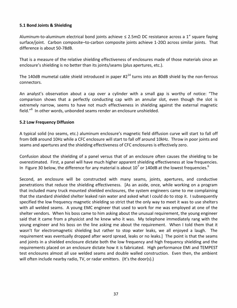
Confusion about the shielding of a panel versus that of an enclosure often causes the shielding to beoverestimated. First, a panel will have much higher apparent shielding effectiveness at low frequencies.In Figure 30 below, the difference for any material is about 107 or 140dB at the lowest frequencies.6
Second, an enclosure will be constructed with many seams, joints, apertures, and conductivepenetrations that reduce the shielding effectiveness. [As an aside, once, while working on a programthat included many truck mounted shielded enclosures, the system engineers came to me complainingthat the standard shielded shelter leaked rain water and asked what I could do to stop it. I subsequentlyspecified the low frequency magnetic shielding so strict that the only way to meet it was to use shelterswith all welded seams. A young EMC engineer that used to work for me was employed at one of theshelter vendors. When his boss came to him asking about the unusual requirement, the young engineersaid that it came from a physicist and he knew who it was. My telephone immediately rang with theyoung engineer and his boss on the line asking me about the requirement. When I told them that itwasn’t for electromagnetic shielding but rather to stop water leaks, we all enjoyed a laugh. Therequirement was eventually dropped after word spread, leaks or no leaks.] The point is that the seamsand joints in a shielded enclosure dictate both the low frequency and high frequency shielding and therequirements placed on an enclosure dictate how it is fabricated. High performance EMI and TEMPESTtest enclosures almost all use welded seams and double walled construction. Even then, the ambientwill often include nearby radio, TV, or radar emitters. (It’s the door(s).)
38
Figure 30. Infinite Plate versus an Enclosure Shielding Attenuation6
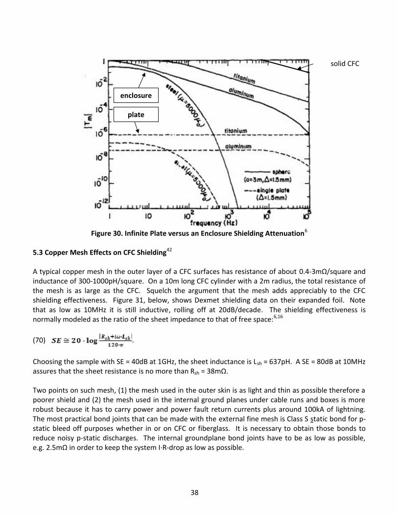
5.3 Copper Mesh Effects on CFC Shielding42
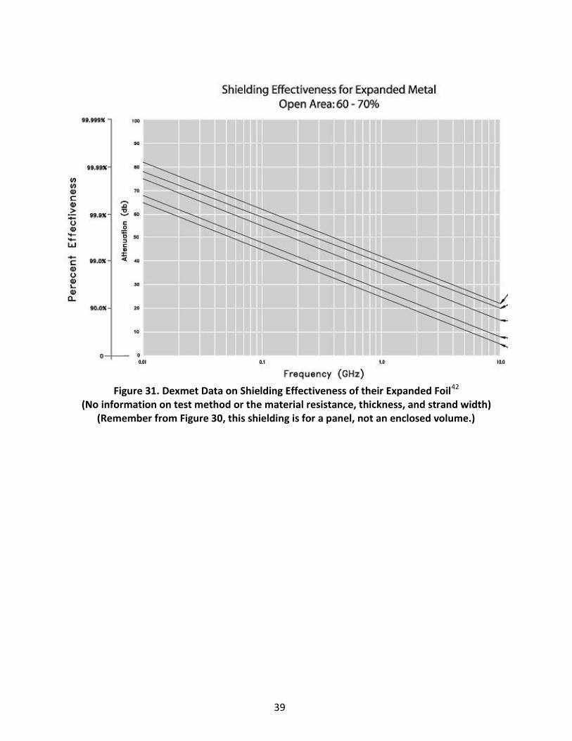
A typical copper mesh in the outer layer of a CFC surfaces has resistance of about 0.4-3mΩ/square andinductance of 300-1000pH/square. On a 10m long CFC cylinder with a 2m radius, the total resistance ofthe mesh is as large as the CFC. Squelch the argument that the mesh adds appreciably to the CFCshielding effectiveness. Figure 31, below, shows Dexmet shielding data on their expanded foil. Notethat as low as 10MHz it is still inductive, rolling off at 20dB/decade. The shielding effectiveness isnormally modeled as the ratio of the sheet impedance to that of free space:6,16
(70) .
Choosing the sample with SE = 40dB at 1GHz, the sheet inductance is Lsh = 637pH. A SE = 80dB at 10MHzassures that the sheet resistance is no more than Rsh = 38mΩ.
Two points on such mesh, (1) the mesh used in the outer skin is as light and thin as possible therefore apoorer shield and (2) the mesh used in the internal ground planes under cable runs and boxes is morerobust because it has to carry power and power fault return currents plus around 100kA of lightning.The most practical bond joints that can be made with the external fine mesh is Class S static bond for p-static bleed off purposes whether in or on CFC or fiberglass. It is necessary to obtain those bonds toreduce noisy p-static discharges. The internal groundplane bond joints have to be as low as possible,e.g. 2.5mΩ in order to keep the system I∙R-drop as low as possible.
enclosure
solid CFCcomposite
plate
39
Figure 31. Dexmet Data on Shielding Effectiveness of their Expanded Foil42
(No information on test method or the material resistance, thickness, and strand width)(Remember from Figure 30, this shielding is for a panel, not an enclosed volume.)
40
5.4 Aircraft Fuel Sensor Protection against Lightning & EMI
Fuel quantity probes are typically vertical coaxial capacitors whose outputs vary with the height offuel inside the probe. They are connected back to the electronics with a shielded twisted pair (TSP) ofwires that fasten differentially across the two coaxial cylinders of the probe. The probes areunshielded from the outside except for the TSP shielding and whatever unintentional shielding thefuel tanks provide. Fuel tanks are seldom constructed to be shielded enclosures because thedesigners don’t want to degrade the corrosion control of the anodized fittings and hatches. Bondingjumpers are the norm for achieving a common electrical connection between all of the fuel systemcomponents and aircraft structure. Bonding jumpers are only good for static bonds because theirinductance is more than the plumbing they’re fastened to.
The fuel probes capacitance to the fuel tanks is due to their proximity to the top and bottom of thetanks. The induced voltage across that capacitance induced by lightning and EMI is the safetyconcern. Common mode and differential induced voltages can cause wrong fuel readings if presentlong enough.
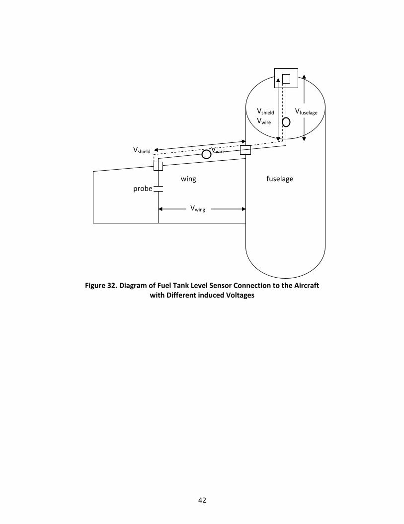
Figure 32, below, illustrates the wiring between the fuel probe and the fuel system electronics. Thetwisted pair is designated as one line. The TSP shield is designated as a dashed line. The capacitanceto both the top and bottom of the fuel tank is designated as one capacitor. The induced voltageacross the capacitor is due to the voltage induced across the fuselage and the wing, Vfuselage + Vwing,between the probe and the end-point electronics. This problem is complicated by the probe notbeing inside a shielded enclosure like the usual electronic load.
The voltage induced across the fuselage and wing is due to the V = I·R-drop from lightning currentthrough the two structures and the structure resistance. That voltage divides across the capacitanceand the load at the other end. That voltage also includes the voltage drop across the cable shield inparallel. In composite-skinned airframes, this voltage can reach 10kV. The cable shield does littlebecause the probe is unshielded. The voltage goes down as the number of other cables andplumbing that parallel it increase in number, shown crudely below; N f is the number of parallelconductors in the fuselage and Nw is the number in the wing.
(71) .
A cable shield ungrounded at either end will offer zero shielding effectiveness up to the quarter-waveresonant frequency of the cable shield where it will then amplify the voltage by say Q ≤ 10.
The probe is a capacitive load therefore the induced voltage across the probe will decrease withincreasing frequency (ignoring resonances), . That makes the inducedvoltage larger at the electronic load on the other end taking away the safety issue of HIRF-inducedvoltage on fuel probes.
Summary. The structural IR voltage drop induces the largest voltage between the probe and the tankwalls.
41
In this simple example, the induced voltage ranges from a max of 100kV down to 200V dependingupon the groundplane, the cable shield thickness, and the number of parallel conductors. Installingwide groundplanes in the wings is difficult because there is no room. Other environmental conditionsmay require a minimum voltage standoff rating for the probes in situ.
Clearly, transformer isolation (of digital signals from an A/D device) and/or optical isolation both withseveral pF capacitance, series current-limiting resistors, and at least 1kV standoff rating is required tomake this susceptibility truly safe.
The fuel tank would have to possess shielding effectiveness equaling or exceeding the cable shield inorder to make this problem depend upon the cable shield only. Fuel system designers are tooprotective of their corrosion resistant non-conducting anodized joints to allow sealing the tanks withconductive seams and joints. They will, however, attach a spider’s web of bonding jumpers acrossalmost all non-conducting joints. This is OK for static discharge grounding but efficient for EMI andlightning only in your dreams. There are also a lot of moveable conductive disconnects in fuel linessubject to high vibration; these are sealed with fitting s that employ gaskets for fuel leaks and havefinger stock that make electrical contact across these moveable joints.
What we’re trying to get across here is that even though there is a lot of conductive plumbingparalleling cable runs in aircraft, taking credit for them in reducing lightning allocations on the cablesis questionable since they do not possess EMI and lightning bonding requirements of, say, 2.5mΩ, juststatic, 1Ω.
The Fully Automated Electronic Control (FADEC) on the engines has a similar problem except that it isfully shielded.
42
Vshield Vfuselage
Vwire
Vshield Vwire
wing fuselageprobe
Vwing
Figure 32. Diagram of Fuel Tank Level Sensor Connection to the Aircraftwith Different induced Voltages
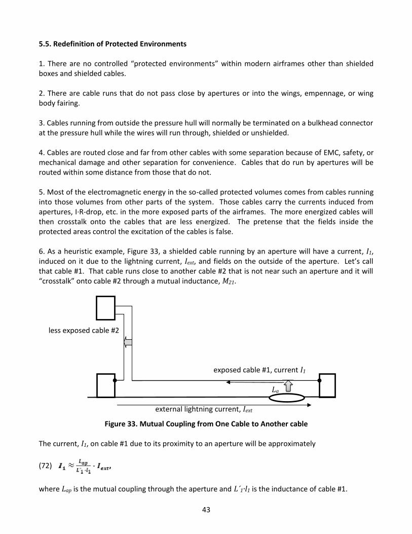
43
5.5. Redefinition of Protected Environments
1. There are no controlled “protected environments” within modern airframes other than shieldedboxes and shielded cables.
2. There are cable runs that do not pass close by apertures or into the wings, empennage, or wingbody fairing.
3. Cables running from outside the pressure hull will normally be terminated on a bulkhead connectorat the pressure hull while the wires will run through, shielded or unshielded.
4. Cables are routed close and far from other cables with some separation because of EMC, safety, ormechanical damage and other separation for convenience. Cables that do run by apertures will berouted within some distance from those that do not.
5. Most of the electromagnetic energy in the so-called protected volumes comes from cables runninginto those volumes from other parts of the system. Those cables carry the currents induced fromapertures, I·R-drop, etc. in the more exposed parts of the airframes. The more energized cables willthen crosstalk onto the cables that are less energized. The pretense that the fields inside theprotected areas control the excitation of the cables is false.
6. As a heuristic example, Figure 33, a shielded cable running by an aperture will have a current, I1,induced on it due to the lightning current, Iext, and fields on the outside of the aperture. Let’s callthat cable #1. That cable runs close to another cable #2 that is not near such an aperture and it will“crosstalk” onto cable #2 through a mutual inductance, M21.
less exposed cable #2
exposed cable #1, current I1
La
external lightning current, Iext
Figure 33. Mutual Coupling from One Cable to Another cable
The current, I1, on cable #1 due to its proximity to an aperture will be approximately
(72) ,
where Lap is the mutual coupling through the aperture and L´1·l1 is the inductance of cable #1.
44
The crosstalk of that current onto another shielded cable #2 is approximately
(73) ,
where M´12·l12 is the mutual magnetic coupling between cables #1 and #2 along a length of cables l12
common to both and L´2·l2 is the inductance of cable #2.
The current induced on cable #2 due to the exterior current, Iext, is then
(74) .
A measure of the “protection” of cable #2 due to its location away from an aperture yet near to cable#1 that runs by an aperture is then written as an attenuation, A,
(75) .
The cables are both at height, h = 1cm, above the groundplane, a distance, d, apart, and have radii, r= 1cm. The mutual inductance is that of two cables above a groundplane:6
(76) with the cable radius, r, included and
(77) with the cable radius, r, set to zero.
The WF4 cable current is set to 10kA and the results can be scaled according to actual levels. Thelengths of parallel routing of the source and receptor cables are l12 = 1m, 2m, and 3m. The inducedWF1 current and WF2 voltage are given as follows:
(78) ;
(79) , where the WF4 rise time, τr = 1.5μs.
These simple formulas are provided so that the lightning engineer can scale his or her resultsaccording to the system situation at hand. I1 (WF1) is plotted in Figure 34 and V2 (WF2) in Figure 35.
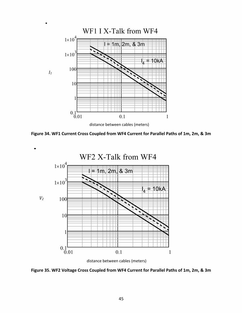
45
0.01 0.1 10.1
1
10
100
1 103
1 104
WF1 I X-Talk from WF4
Im 1
Im 2
Im 3
dm
l = 1m, 2m, & 3m
I4 = 10kA
Figure 34. WF1 Current Cross Coupled from WF4 Current for Parallel Paths of 1m, 2m, & 3m
0.01 0.1 10.1
1
10
100
1 103
1 104
WF2 X-Talk from WF4
V1 m
V2 m
V3 m
dm
l = 1m, 2m, & 3m
I4 = 10kA
Figure 35. WF2 Voltage Cross Coupled from WF4 Current for Parallel Paths of 1m, 2m, & 3m
I1
V2
distance between cables (meters)
distance between cables (meters)
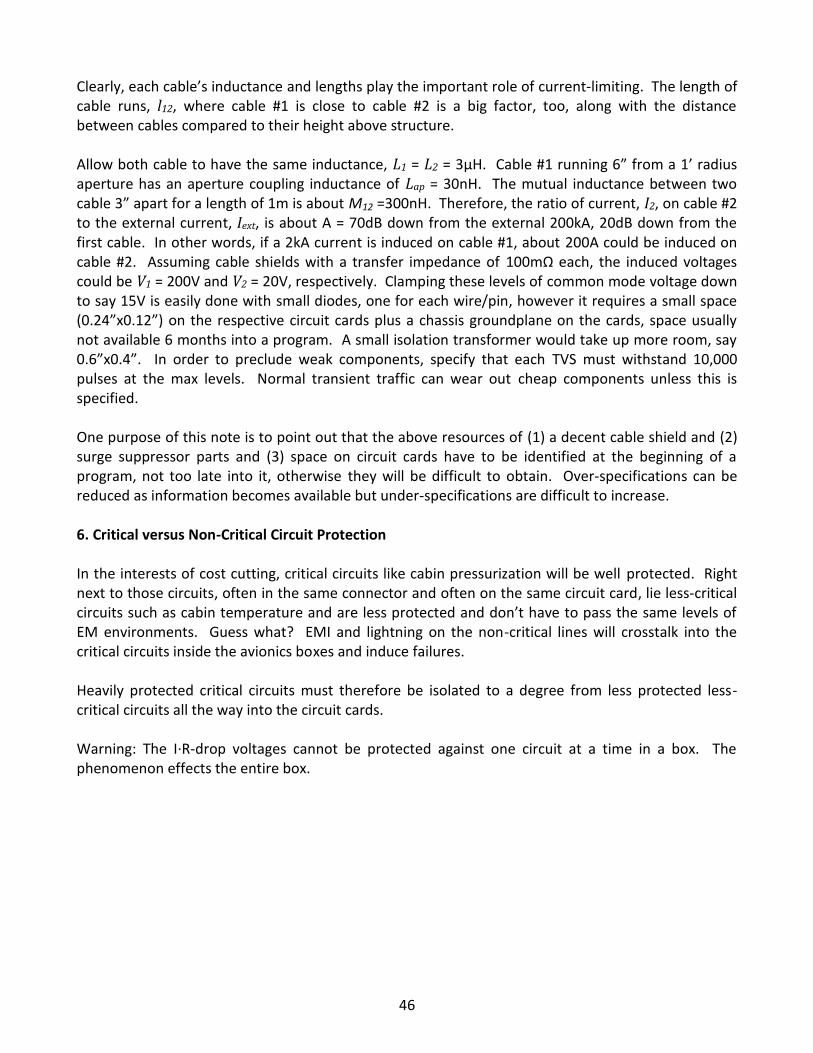
46
Clearly, each cable’s inductance and lengths play the important role of current-limiting. The length ofcable runs, l12, where cable #1 is close to cable #2 is a big factor, too, along with the distancebetween cables compared to their height above structure.
Allow both cable to have the same inductance, L1 = L2 = 3µH. Cable #1 running 6” from a 1’ radiusaperture has an aperture coupling inductance of Lap = 30nH. The mutual inductance between twocable 3” apart for a length of 1m is about M12 =300nH. Therefore, the ratio of current, I2, on cable #2to the external current, Iext, is about A = 70dB down from the external 200kA, 20dB down from thefirst cable. In other words, if a 2kA current is induced on cable #1, about 200A could be induced oncable #2. Assuming cable shields with a transfer impedance of 100mΩ each, the induced voltagescould be V1 = 200V and V2 = 20V, respectively. Clamping these levels of common mode voltage downto say 15V is easily done with small diodes, one for each wire/pin, however it requires a small space(0.24”x0.12”) on the respective circuit cards plus a chassis groundplane on the cards, space usuallynot available 6 months into a program. A small isolation transformer would take up more room, say0.6”x0.4”. In order to preclude weak components, specify that each TVS must withstand 10,000pulses at the max levels. Normal transient traffic can wear out cheap components unless this isspecified.
One purpose of this note is to point out that the above resources of (1) a decent cable shield and (2)surge suppressor parts and (3) space on circuit cards have to be identified at the beginning of aprogram, not too late into it, otherwise they will be difficult to obtain. Over-specifications can bereduced as information becomes available but under-specifications are difficult to increase.
6. Critical versus Non-Critical Circuit Protection
In the interests of cost cutting, critical circuits like cabin pressurization will be well protected. Rightnext to those circuits, often in the same connector and often on the same circuit card, lie less-criticalcircuits such as cabin temperature and are less protected and don’t have to pass the same levels ofEM environments. Guess what? EMI and lightning on the non-critical lines will crosstalk into thecritical circuits inside the avionics boxes and induce failures.
Heavily protected critical circuits must therefore be isolated to a degree from less protected less-critical circuits all the way into the circuit cards.
Warning: The I∙R-drop voltages cannot be protected against one circuit at a time in a box. Thephenomenon effects the entire box.
47
7. Electrical Components Mounted on the Exterior Exposed to Direct Strikes
Components mounted on the exterior are considered sacrificial when directly struck by lightning.However, we need to prevent the resulting lightning-induced transients from getting inside andcausing damage to other hardware. The first job is to determine the zones these components arelocated. Then, apply surge protection as close to the external components as possible so as to stopthe lightning from penetrating into the system any further, examples shown in Table 13.
Table 13. Typical Protection on External Components to keep Lightning from the Interior
External Component Protection Suggestions Notes
Antennas ¼-wave stubs, gas surge arrestors residual voltage ≈ 15V
Pitot & temp diode clamps 100kW
Lights diode clamps 100kW
Open connectors TBD pending zoning assessment (usually not a concern)
Control surface sensors diode clamps 100kW
WOW*, brakes, & sensors diode clamps 100kW
Windshield deicingconducting film
diode clamps plus inductive filter, if possible 100kW
Note: * WOW are the weight on wheel switches in the landing gear that disengage the autopilot andother automatic controls upon touchdown.
8. Nearby Lightning Strikes, Fields and Coupling
Magnetic fields close to a lightning strike follow Ampere’s law.
(80) .
The open circuit voltage induced in nearby vertical loops of area A = l∙h follows faraday’s law.
(81) .
A 200kA lightning strike 100m away can induce 200 volts in a 10m long cable 3” off of structure, 2kVwhen 10m away. This is enough to cause damage if not mitigated. This is both an airborne and aground problem. See Section 13, below, for ground surge protection.
9. Ground Operations Surge Requirements
Aerospace EMI/EMC and lightning requirements documents are characteristically silent on groundoperations. MIL-STD-461C showed a healthy respect for ground surge environments by making CS06power surge on GSE power connections x2 larger than that for operational systems unconnected toGSE.
48
Besides lightning, normal ground power transients can wear out components. The USN put CS106back into part of MIL-STD-461F43 with the following rationale, far too practical and experienced formost pedants:
“The Navy submarine community has found the obsolete CS06 of MIL-STD-461 (through revisionC) requirement to be an effective method to minimize risk of transient related equipment andsubsystem susceptibility. This type of transient susceptibility test has been successful in earlyidentification of transient related EMI problems in naval equipment and subsystems. The Navyhas found good correlation between transient related shipboard problems, including longevity,degraded performance, premature failures, and CS106 susceptibilities.”
IEEE and ANSI have more experience to add:32
“Surge voltages occurring in low-voltage ac power circuits originate from two major sources:lightning effects (direct or indirect) on the power system and system switching transients. Therate of occurrence of surges varies over wide limits, depending upon the particular powersystem. Prediction of the rate for a particular system is always difficult and frequentlyimpossible. The rate is related to the level of the surges; low-level surges are more prevalentthan high-level surges. The frequency of surges is a key indicator of their damage potential.”
Typical ground surges are specified as follows in Table 14 depending upon location and the degree ofbuilding lightning protection:
Table 14. Comparing Lightning Standards inside a FacilityNFPA 780,31 ANSI/IEEE C62.41,32 & IEC 61000 4-533
NFPA 780 A.4.18.3.1 ANSI/IEEE C62.41 IEC 61000-4-5Service entry – 40kA Category C – 3-10kA, 6-20kV Class 4 – 4kVBranch panels – 20kA Category B – 1-3kA, 2-6kV Class 3 – 2kVPoint of utilization – 10kA Category A – 70-200A, 2-6kV Class 2 – 1kV
The very different levels are indicative of the different committees and their charters. The ANSI/IEEEC62.41 documents appear to be the most researched and complete. The point is that any system onthe ground must be able to withstand such surges on ground connections depending upon theprotection provided by the host facility. A list of US and European standards that address powersurges and lightning protection of facilities and the equipment inside are the following:
NFPA 780, Standard for the Installation of Lightning Protection Systems31
ANSI/IEEE C62.41-1991, IEEE Recommended Practice in Low Voltage AC Power Circuits32
IEC 61000 4-5, Equipment Classification of Power Surge and Lightning Protection33
All too often, everyone focuses on in-flight issues and turn a blind eye towards ground operations,ground support equipment including power sources, and test.
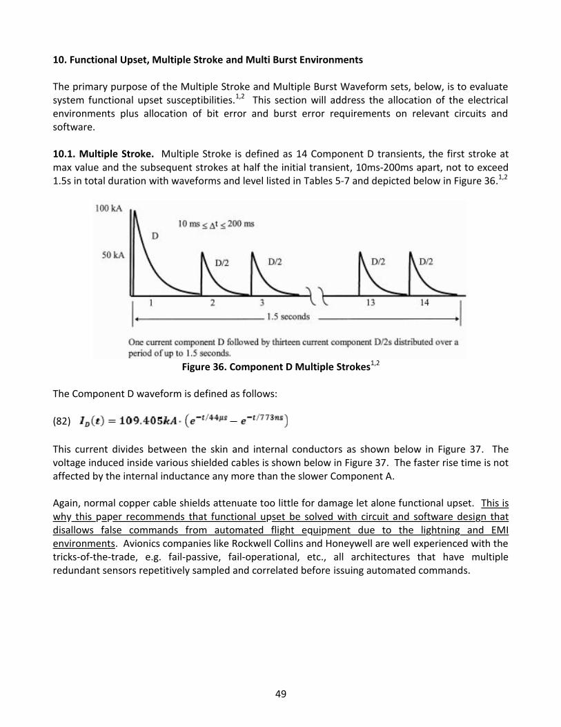
49
10. Functional Upset, Multiple Stroke and Multi Burst Environments
The primary purpose of the Multiple Stroke and Multiple Burst Waveform sets, below, is to evaluatesystem functional upset susceptibilities.1,2 This section will address the allocation of the electricalenvironments plus allocation of bit error and burst error requirements on relevant circuits andsoftware.
10.1. Multiple Stroke. Multiple Stroke is defined as 14 Component D transients, the first stroke atmax value and the subsequent strokes at half the initial transient, 10ms-200ms apart, not to exceed1.5s in total duration with waveforms and level listed in Tables 5-7 and depicted below in Figure 36.1,2
Figure 36. Component D Multiple Strokes1,2
The Component D waveform is defined as follows:
(82)
This current divides between the skin and internal conductors as shown below in Figure 37. Thevoltage induced inside various shielded cables is shown below in Figure 37. The faster rise time is notaffected by the internal inductance any more than the slower Component A.
Again, normal copper cable shields attenuate too little for damage let alone functional upset. This iswhy this paper recommends that functional upset be solved with circuit and software design thatdisallows false commands from automated flight equipment due to the lightning and EMIenvironments. Avionics companies like Rockwell Collins and Honeywell are well experienced with thetricks-of-the-trade, e.g. fail-passive, fail-operational, etc., all architectures that have multipleredundant sensors repetitively sampled and correlated before issuing automated commands.
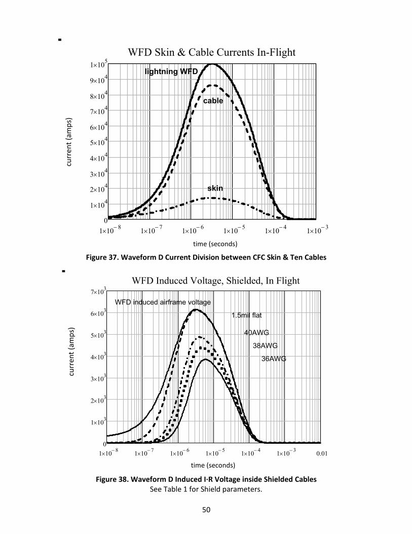
50
1 10 8 1 10 7 1 10 6 1 10 5 1 10 4 1 10 30
1 104
2 104
3 104
4 104
5 104
6 104
7 104
8 104
9 104
1 105
WFD Skin & Cable Currents In-Flight
Is1 n( )
Ic1 n( )
ID n( )
t n( )
lightning WFD
cable
skin
Figure 37. Waveform D Current Division between CFC Skin & Ten Cables
1 10 8 1 10 7 1 10 6 1 10 5 1 10 4 1 10 3 0.010
1 103
2 103
3 103
4 103
5 103
6 103
7 103
WFD Induced Voltage, Shielded, In Flight
Ics4 n( )
Ics1 n( )
Ics2 n( )
Ics3 n( )
Vs1 n( )
t n( )
WFD induced airframe voltage
1.5mil flat
40AWG
38AWG
36AWG
Figure 38. Waveform D Induced I∙R Voltage inside Shielded CablesSee Table 1 for Shield parameters.
curr
ent (
amps
)
time (seconds)
time (seconds)
curr
ent (
amps
)
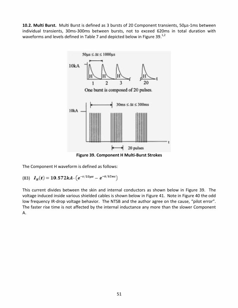
51
10.2. Multi Burst. Multi Burst is defined as 3 bursts of 20 Component transients, 50μs-1ms betweenindividual transients, 30ms-300ms between bursts, not to exceed 620ms in total duration withwaveforms and levels defined in Table 7 and depicted below in Figure 39.1,2
Figure 39. Component H Multi-Burst Strokes
The Component H waveform is defined as follows:
(83)
This current divides between the skin and internal conductors as shown below in Figure 39. Thevoltage induced inside various shielded cables is shown below in Figure 41. Note in Figure 40 the oddlow frequency IR-drop voltage behavior. The NTSB and the author agree on the cause, “pilot error”.The faster rise time is not affected by the internal inductance any more than the slower ComponentA.
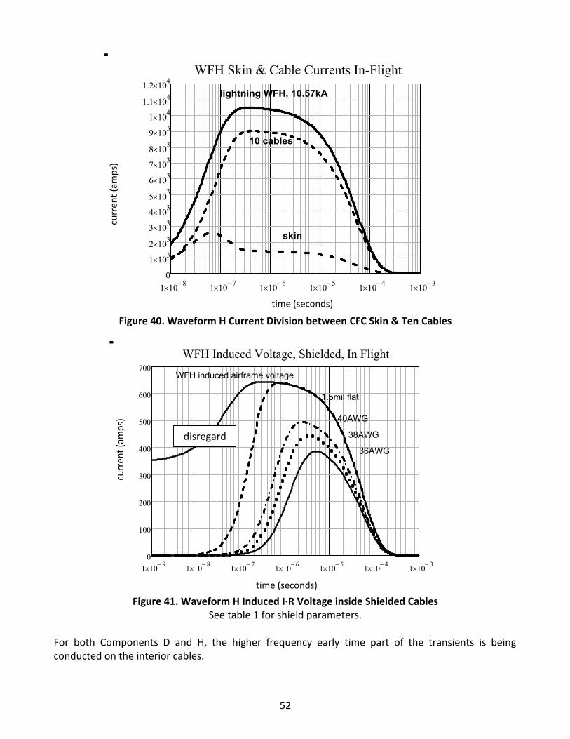
52
1 10 8 1 10 7 1 10 6 1 10 5 1 10 4 1 10 30
1 103
2 103
3 103
4 103
5 103
6 103
7 103
8 103
9 103
1 104
1.1 104
1.2 104
WFH Skin & Cable Currents In-Flight
Is1 n( )
Ic1 n( )
IH n( )
t n( )
lightning WFH, 10.57kA
10 cables
skin
Figure 40. Waveform H Current Division between CFC Skin & Ten Cables
1 10 9 1 10 8 1 10 7 1 10 6 1 10 5 1 10 4 1 10 30
100
200
300
400
500
600
700WFH Induced Voltage, Shielded, In Flight
Ics4 n( )
Ics1 n( )
Ics2 n( )
Ics3 n( )
Vs1 n( )
t n( )
WFH induced airframe voltage
1.5mil flat
40AWG
38AWG
36AWG
Figure 41. Waveform H Induced I∙R Voltage inside Shielded CablesSee table 1 for shield parameters.
For both Components D and H, the higher frequency early time part of the transients is beingconducted on the interior cables.
disregard
time (seconds)
curr
ent (
amps
)cu
rren
t (am
ps)
time (seconds)
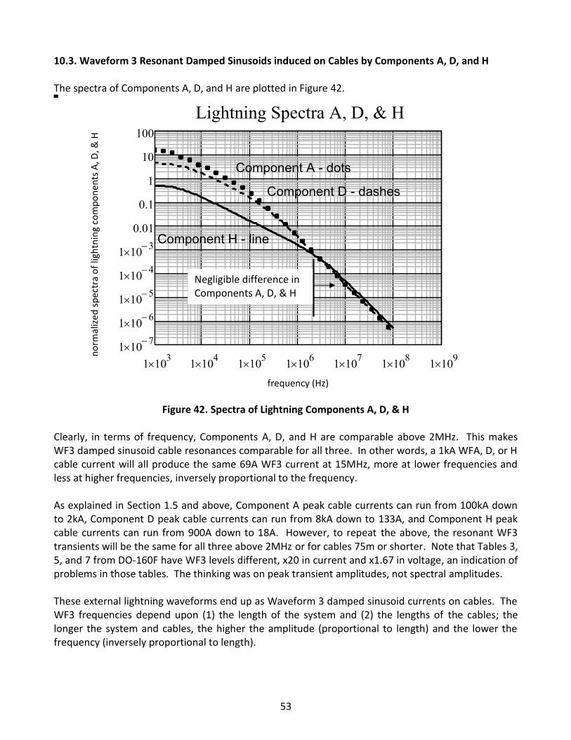
53
10.3. Waveform 3 Resonant Damped Sinusoids induced on Cables by Components A, D, and H
The spectra of Components A, D, and H are plotted in Figure 42.
1 103 1 104 1 105 1 106 1 107 1 108 1 1091 10 7
1 10 6
1 10 5
1 10 4
1 10 3
0.01
0.1
1
10
100Lightning Spectra A, D, & H
Sa m( )
SD m( )
SH m( )
f m( )
Component A - dots
Component D - dashes
Component H - line
Figure 42. Spectra of Lightning Components A, D, & H
Clearly, in terms of frequency, Components A, D, and H are comparable above 2MHz. This makesWF3 damped sinusoid cable resonances comparable for all three. In other words, a 1kA WFA, D, or Hcable current will all produce the same 69A WF3 current at 15MHz, more at lower frequencies andless at higher frequencies, inversely proportional to the frequency.
As explained in Section 1.5 and above, Component A peak cable currents can run from 100kA downto 2kA, Component D peak cable currents can run from 8kA down to 133A, and Component H peakcable currents can run from 900A down to 18A. However, to repeat the above, the resonant WF3transients will be the same for all three above 2MHz or for cables 75m or shorter. Note that Tables 3,5, and 7 from DO-160F have WF3 levels different, x20 in current and x1.67 in voltage, an indication ofproblems in those tables. The thinking was on peak transient amplitudes, not spectral amplitudes.
These external lightning waveforms end up as Waveform 3 damped sinusoid currents on cables. TheWF3 frequencies depend upon (1) the length of the system and (2) the lengths of the cables; thelonger the system and cables, the higher the amplitude (proportional to length) and the lower thefrequency (inversely proportional to length).
Negligible difference inComponents A, D, & H
frequency (Hz)
norm
aliz
ed s
pect
ra o
f lig
htni
ng c
ompo
nent
s A
, D, &
H
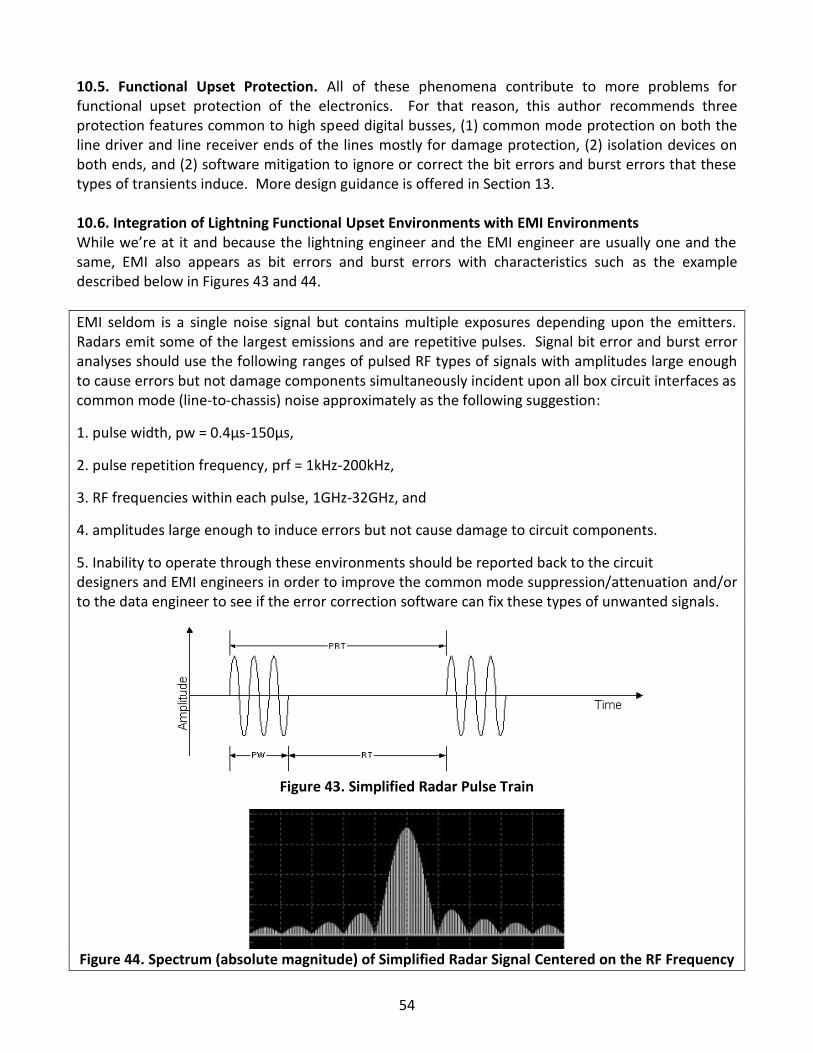
54
10.5. Functional Upset Protection. All of these phenomena contribute to more problems forfunctional upset protection of the electronics. For that reason, this author recommends threeprotection features common to high speed digital busses, (1) common mode protection on both theline driver and line receiver ends of the lines mostly for damage protection, (2) isolation devices onboth ends, and (2) software mitigation to ignore or correct the bit errors and burst errors that thesetypes of transients induce. More design guidance is offered in Section 13.
10.6. Integration of Lightning Functional Upset Environments with EMI EnvironmentsWhile we’re at it and because the lightning engineer and the EMI engineer are usually one and thesame, EMI also appears as bit errors and burst errors with characteristics such as the exampledescribed below in Figures 43 and 44.
EMI seldom is a single noise signal but contains multiple exposures depending upon the emitters.Radars emit some of the largest emissions and are repetitive pulses. Signal bit error and burst erroranalyses should use the following ranges of pulsed RF types of signals with amplitudes large enoughto cause errors but not damage components simultaneously incident upon all box circuit interfaces ascommon mode (line-to-chassis) noise approximately as the following suggestion:
1. pulse width, pw = 0.4μs-150μs,
2. pulse repetition frequency, prf = 1kHz-200kHz,
3. RF frequencies within each pulse, 1GHz-32GHz, and
4. amplitudes large enough to induce errors but not cause damage to circuit components.
5. Inability to operate through these environments should be reported back to the circuitdesigners and EMI engineers in order to improve the common mode suppression/attenuation and/orto the data engineer to see if the error correction software can fix these types of unwanted signals.
Figure 43. Simplified Radar Pulse Train
Figure 44. Spectrum (absolute magnitude) of Simplified Radar Signal Centered on the RF Frequency
55
11. HIRF versus Lightning
Lightning consultants and engineers are being asked about high intensity radio frequency (HIRF)environments as compared to lightning induced environments.25 A representative set of HIRFenvironments are shown in Table 15.4,22 Do not take these specific levels seriously as they are subjectto change with every new revision of the requirements.
Quite simply, the peak induced voltage on a cable of height, h, above structure due to an incidentelectric field, E, is V = E·h plus resonances, V ≈ Q·E·h, where Q is the cable resonant Q-factor, Q ≈ 10.Induced currents are that voltage divided by the transmission line surge impedance, Z0 ≈ 100-300Ω or
, where B is the incident magnetic flux, B = E/c. See Figure 3. The so called “antennamode’ with the E-field incident parallel to the cable is not considered because all cables in systemsare mounted close to structure; that means that the sum of the incident and reflected E-fields isabout 60dB down from the incident E-field. The magnetic field is considered, however.
For an exposed cable 1” above structure and a HIRF E-field strength of 3kV/m, the induced voltage isV = E·h = 76V times the resonant Q-values, V = 760V at the first resonant peak, and the inducedcurrent is about I = BA/L = 750mA times the resonant Q-values, I = 7.5A at the first resonant peak,both independent of cable length and both roll off exponentially with increasing frequency above thefirst resonance. HIRF induced currents can be shielded much better than low frequency broadbandindirect lightning transients, i.e. a 100mΩ cable shield transfer impedance will reduce 7.5A to 750mVinduced in the shielded wires, 10mΩ transfer impedance will result in 75mV induced voltage,common mode. Lightning excitation will be mostly a V = I∙R-drop in the shields, not a V = iω∙L in thewires.15 (See Figure 22.) Cable shield transfer impedances level off to about 200mΩ to 2Ω above afew tens of MHz (See Figure 22.), therefore each situation must be evaluated separately. Commonmode mitigation in the I/O circuitry can reduce both EMI and lightning another 20dB or more.However, isolation plus voltage clamping is the more likely successful lightning fix for the I∙R-drop inchassis ground. One more fact: good EMC control will keep internal noise levels low so thatexternally generated noise has more margin.
Cable resonances rarely exceed Q ≈ 10 at lower frequencies and decrease with frequency. Likewise,HIRF high frequencies do not propagate very far down electrical cables. Therefore, in terms of cablecoupling, HIRF does not compete with indirect lightning with kilo-amps of current. The worst HIRFthreat to electronics is through line-of-sight coupling to RF antennas and apertures in equipment withsensitive electronics inside, e.g. burn out of RF front ends like GPS, ILS, etc. and disruption or damageto optical sensors and “glass cockpit” electronics with many large LED or plasma displays.
Lightning protection will improve the low frequency noise mitigation and HIRF protection willimprove the high frequency noise mitigation. Lightning still has to work harder to obtain protection;for instance, adding a second layer of copper wire braid cable shield will improve HIRF protection by20db while lightning protection only gets 6dB. In difficult lightning shielding situations, adding a layerof mumetal foil is needed; HIRF benefits because of the near 100% optical coverage and the lossynature of the mumetal.
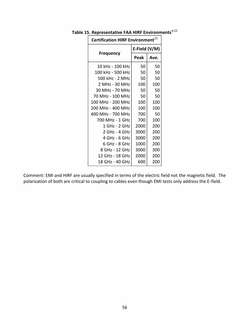
56
Table 15. Representative FAA HIRF Environments4,22
Comment: EMI and HIRF are usually specified in terms of the electric field not the magnetic field. Thepolarization of both are critical to coupling to cables even though EMI tests only address the E-field.
Certification HIRF Environment22
FrequencyE-Field (V/M)
Peak Ave.
10 kHz - 100 kHz100 kHz - 500 kHz
500 kHz - 2 MHz2 MHz - 30 MHz
30 MHz - 70 MHz70 MHz - 100 MHz
100 MHz - 200 MHz200 MHz - 400 MHz400 MHz - 700 MHz
700 MHz - 1 GHz1 GHz - 2 GHz2 GHz - 4 GHz4 GHz - 6 GHz6 GHz - 8 GHz
8 GHz - 12 GHz12 GHz - 18 GHz18 GHz - 40 GHz
505050
1005050
100100700700
200030003000100030002000
600
505050
1005050
100100
50100200200200200300200200
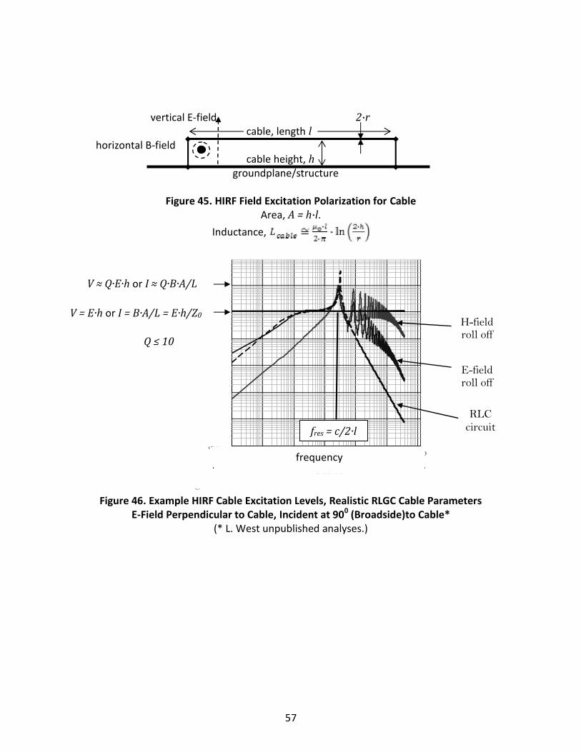
57
vertical E-field 2∙rcable, length l
horizontal B-fieldcable height, h
groundplane/structure
Figure 45. HIRF Field Excitation Polarization for CableArea, A = h∙l.
Inductance,
0.258536
7.23188210 7
VHHB n( )
VEVB n( )
VC n( )
VEinc
3 1091 104 f n( )1 104 1 105 1 106 1 107 1 108 1 109 1 1010
1 10 7
1 10 6
1 10 5
1 10 4
1 10 3
0.01
0.1
1H-(HH) & E-(VE) broad-fire & VE-Circuit
fre que ncy
right
han
d lo
ad v
olta
ge
Figure 7.2. Broadside Excitation, E = 10V/m
E-fieldroll off
H-fieldroll off
RLCcircuit
Figure 46. Example HIRF Cable Excitation Levels, Realistic RLGC Cable ParametersE-Field Perpendicular to Cable, Incident at 900 (Broadside)to Cable*
(* L. West unpublished analyses.)
V = E·h or I = B·A/L = E·h/Z0
V ≈ Q·E·h or I ≈ Q·B·A/L
fres = c/2·l
Q ≤ 10
frequency
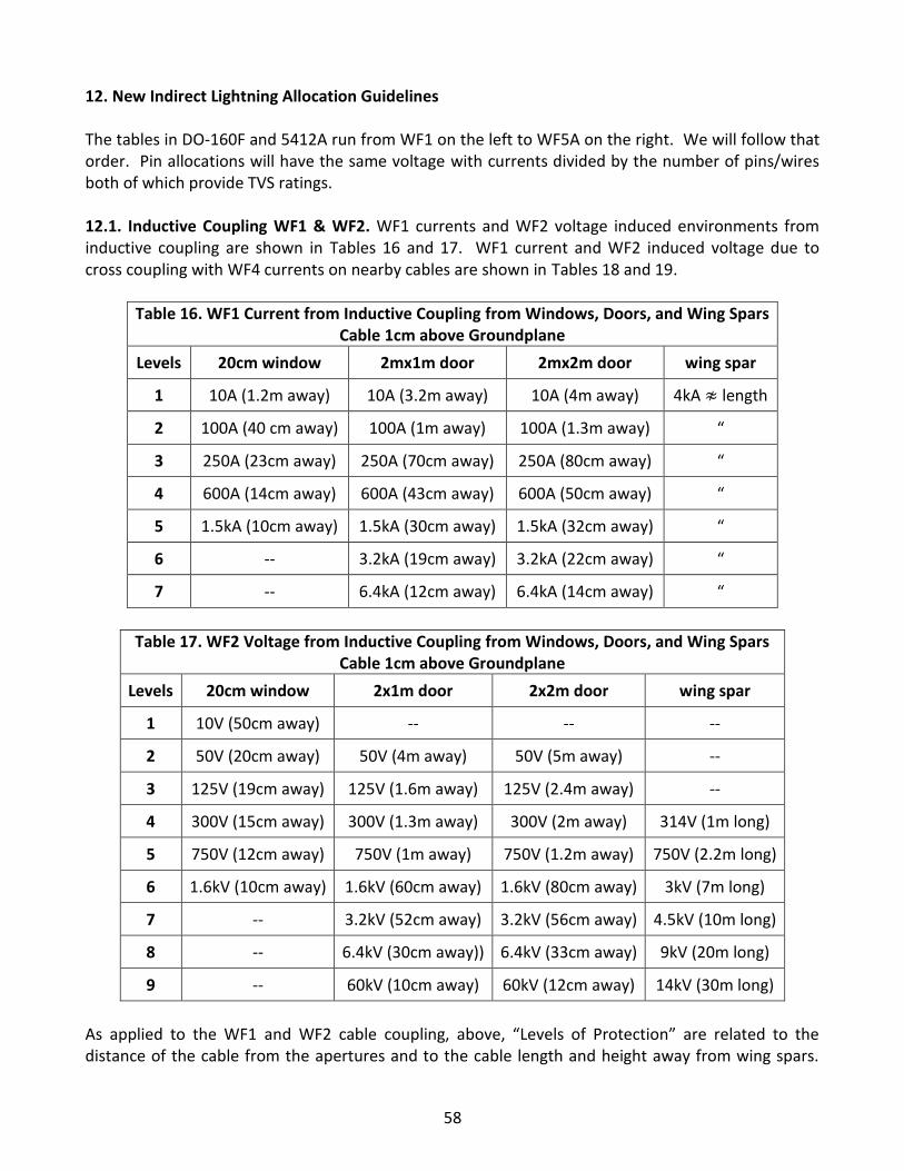
58
12. New Indirect Lightning Allocation Guidelines
The tables in DO-160F and 5412A run from WF1 on the left to WF5A on the right. We will follow thatorder. Pin allocations will have the same voltage with currents divided by the number of pins/wiresboth of which provide TVS ratings.
12.1. Inductive Coupling WF1 & WF2. WF1 currents and WF2 voltage induced environments frominductive coupling are shown in Tables 16 and 17. WF1 current and WF2 induced voltage due tocross coupling with WF4 currents on nearby cables are shown in Tables 18 and 19.
Table 16. WF1 Current from Inductive Coupling from Windows, Doors, and Wing SparsCable 1cm above Groundplane
Levels 20cm window 2mx1m door 2mx2m door wing spar
1 10A (1.2m away) 10A (3.2m away) 10A (4m away) 4kA ≉ length
2 100A (40 cm away) 100A (1m away) 100A (1.3m away) “
3 250A (23cm away) 250A (70cm away) 250A (80cm away) “
4 600A (14cm away) 600A (43cm away) 600A (50cm away) “
5 1.5kA (10cm away) 1.5kA (30cm away) 1.5kA (32cm away) “
6 -- 3.2kA (19cm away) 3.2kA (22cm away) “
7 -- 6.4kA (12cm away) 6.4kA (14cm away) “
Table 17. WF2 Voltage from Inductive Coupling from Windows, Doors, and Wing SparsCable 1cm above Groundplane
Levels 20cm window 2x1m door 2x2m door wing spar
1 10V (50cm away) -- -- --
2 50V (20cm away) 50V (4m away) 50V (5m away) --
3 125V (19cm away) 125V (1.6m away) 125V (2.4m away) --
4 300V (15cm away) 300V (1.3m away) 300V (2m away) 314V (1m long)
5 750V (12cm away) 750V (1m away) 750V (1.2m away) 750V (2.2m long)
6 1.6kV (10cm away) 1.6kV (60cm away) 1.6kV (80cm away) 3kV (7m long)
7 -- 3.2kV (52cm away) 3.2kV (56cm away) 4.5kV (10m long)
8 -- 6.4kV (30cm away)) 6.4kV (33cm away) 9kV (20m long)
9 -- 60kV (10cm away) 60kV (12cm away) 14kV (30m long)
As applied to the WF1 and WF2 cable coupling, above, “Levels of Protection” are related to thedistance of the cable from the apertures and to the cable length and height away from wing spars.
59
Table 18. WF1 Current from Cable Cross Coupling to 10kA WF4Groundplane Present
Levelsrequired cable separation
range: l12 common length = 3, 2, & 1mInduced WF1
1 d = 8-12cm 100A
2 d = 5-10cm 250A
3 d = 2-6cm 600A
4 d = 2-3cm 1.5kA
5 d = 1cm 3.2kA
Table 19. WF2 Voltage from Cable Cross Coupling to 10kA WF4Groundplane Present
Levelsrequired cable separation
range: l12 common length = 3, 2, & 1mInduced WF2
1 d = 7-13cm 50V
2 d = 6-12cm 125V
3 d = 3-8cm 300V
4 d = 1.3-5cm 750V
5 d = 1-2cm 1.6kV
For each Level of Protection from the DO-160F and SAE ARP5412A tables, the required cableseparation distances are comparable for induced WF1 currents and WF2 voltages. These are the realLevels of Protection, cable cross coupling instead of bogus shielding attenuation; that is, the lessexposed cables are excited by nearby exposed cables, NOT fields in the region allegedly penetratingfrom outside the system (and badly measured, also). Transport aircraft have more space to routecables; general aviation business and private aircraft have far less space.
60
12.2. Waveform 3 Environments
WF3 is generated by resonances on cables excited by (1) aperture coupling from externalComponents A, D, & H, (2) wing spar coupling from the same, and (3) cables with current from theWF4, D, & H I∙R-drop that resonate at f3 = c/2∙lcable with amplitudes proportional to the length,summarized in Table 20. Scaling the environments is supplied below. Any WF3 excited on the CFCskin will not be treated in this note because of its complexity and small Q. See Tables 17 & 19 for firstorder estimated of WF3 voltages.
Table 20. WF3 Current from Windows, Doors, & Wing WF1 & Wing & Fuselage WF4 I∙R-Dropl(m)
cablef3
window WF1 door WF1 wing WF1 wing WF4 fuselage WF4WF1 WF3 WF1 WF3 WF1 WF3 WF4 WF3 WF4 WF3
1 150MHz 14A 9mA 100A 670mA 4kA 2.7A 12kA 8A 12kA 8A2 75MHz “ 18mA “ 1.3A “ 5.4A 16A “ 16A3 50MHz “ 27mA “ 2A “ 8A 24A “ 24A4 37MHz “ 36mA “ 2.7A “ 11A 32A “ 32A5 30MHz “ 45mA “ 3.4A “ 14A 40A “ 40A
10 15MHz “ 90mA “ 6.7A “ 28A 80A “ 80A20 7.5MHz “ 180mA “ 13A “ 56A 160A “ 160A30 5MHz “ 270mA “ 20A “ 80A 240A “ 240A60 2.5MHz “ 540mA “ 40A “ 160A 480A “ 480A
100 1.5MHz “ 900mA “ 67A “ 280A 800A “ 800ANote: DO-160F WF3 currents ranges from 20A to 640A.
The WF1, WF4, and WF3 levels, above in Table 19, scale up or down as follows where r is theaperture size, d is the distance of cables from apertures, h is the height of the cables above thegroundplane, and Rsystem is the radius of the system at the aperture location:
(84) ;
(85) ;
(86) ;
(87) , where a = wing chord & b = wing camber;
(88) , where
(89) with no groundplane
(90) for the groundplane
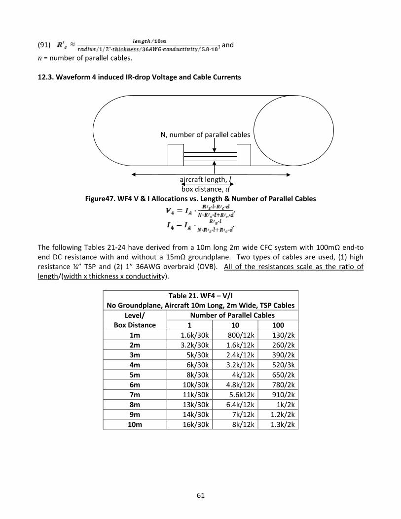
61
(91) and
n = number of parallel cables.
12.3. Waveform 4 induced IR-drop Voltage and Cable Currents
N, number of parallel cables
aircraft length, lbox distance, d
Figure47. WF4 V & I Allocations vs. Length & Number of Parallel Cables
.
.
The following Tables 21-24 have derived from a 10m long 2m wide CFC system with 100mΩ end-toend DC resistance with and without a 15mΩ groundplane. Two types of cables are used, (1) highresistance ¼” TSP and (2) 1” 36AWG overbraid (OVB). All of the resistances scale as the ratio oflength/(width x thickness x conductivity).
Table 21. WF4 – V/INo Groundplane, Aircraft 10m Long, 2m Wide, TSP Cables
Level/Box Distance
Number of Parallel Cables1 10 100
1m 1.6k/30k 800/12k 130/2k2m 3.2k/30k 1.6k/12k 260/2k3m 5k/30k 2.4k/12k 390/2k4m 6k/30k 3.2k/12k 520/3k5m 8k/30k 4k/12k 650/2k6m 10k/30k 4.8k/12k 780/2k7m 11k/30k 5.6k12k 910/2k8m 13k/30k 6.4k/12k 1k/2k9m 14k/30k 7k/12k 1.2k/2k
10m 16k/30k 8k/12k 1.3k/2k
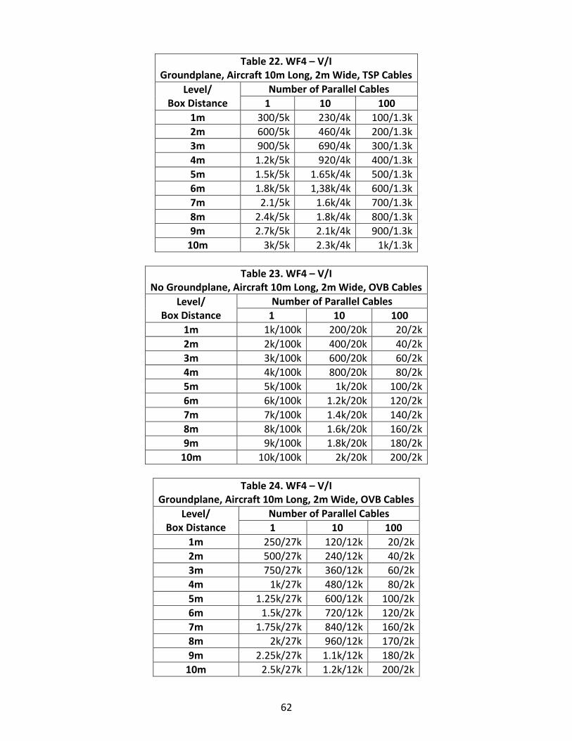
62
Table 22. WF4 – V/IGroundplane, Aircraft 10m Long, 2m Wide, TSP Cables
Level/Box Distance
Number of Parallel Cables1 10 100
1m 300/5k 230/4k 100/1.3k2m 600/5k 460/4k 200/1.3k3m 900/5k 690/4k 300/1.3k4m 1.2k/5k 920/4k 400/1.3k5m 1.5k/5k 1.65k/4k 500/1.3k6m 1.8k/5k 1,38k/4k 600/1.3k7m 2.1/5k 1.6k/4k 700/1.3k8m 2.4k/5k 1.8k/4k 800/1.3k9m 2.7k/5k 2.1k/4k 900/1.3k
10m 3k/5k 2.3k/4k 1k/1.3k
Table 23. WF4 – V/INo Groundplane, Aircraft 10m Long, 2m Wide, OVB Cables
Level/Box Distance
Number of Parallel Cables1 10 100
1m 1k/100k 200/20k 20/2k2m 2k/100k 400/20k 40/2k3m 3k/100k 600/20k 60/2k4m 4k/100k 800/20k 80/2k5m 5k/100k 1k/20k 100/2k6m 6k/100k 1.2k/20k 120/2k7m 7k/100k 1.4k/20k 140/2k8m 8k/100k 1.6k/20k 160/2k9m 9k/100k 1.8k/20k 180/2k
10m 10k/100k 2k/20k 200/2k
Table 24. WF4 – V/IGroundplane, Aircraft 10m Long, 2m Wide, OVB Cables
Level/Box Distance
Number of Parallel Cables1 10 100
1m 250/27k 120/12k 20/2k2m 500/27k 240/12k 40/2k3m 750/27k 360/12k 60/2k4m 1k/27k 480/12k 80/2k5m 1.25k/27k 600/12k 100/2k6m 1.5k/27k 720/12k 120/2k7m 1.75k/27k 840/12k 160/2k8m 2k/27k 960/12k 170/2k9m 2.25k/27k 1.1k/12k 180/2k
10m 2.5k/27k 1.2k/12k 200/2k
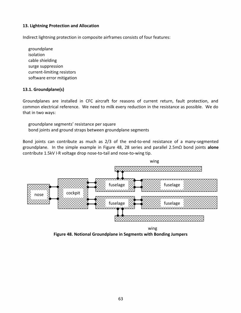
63
13. Lightning Protection and Allocation
Indirect lightning protection in composite airframes consists of four features:
groundplaneisolationcable shieldingsurge suppressioncurrent-limiting resistorssoftware error mitigation
13.1. Groundplane(s)
Groundplanes are installed in CFC aircraft for reasons of current return, fault protection, andcommon electrical reference. We need to milk every reduction in the resistance as possible. We dothat in two ways:
groundplane segments’ resistance per squarebond joints and ground straps between groundplane segments
Bond joints can contribute as much as 2/3 of the end-to-end resistance of a many-segmentedgroundplane. In the simple example in Figure 48, 28 series and parallel 2.5mΩ bond joints alonecontribute 1.5kV I·R voltage drop nose-to-tail and nose-to-wing tip.
Figure 48. Notional Groundplane in Segments with Bonding Jumpers
fuselagefuselage
nose cockpit
fuselagefuselage
wing
wing
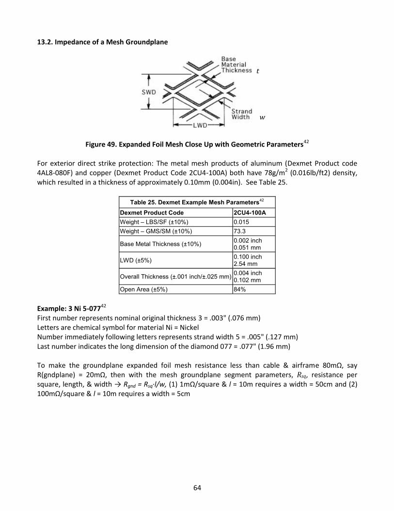
64
13.2. Impedance of a Mesh Groundplane
Figure 49. Expanded Foil Mesh Close Up with Geometric Parameters42
For exterior direct strike protection: The metal mesh products of aluminum (Dexmet Product code4AL8-080F) and copper (Dexmet Product Code 2CU4-100A) both have 78g/m2 (0.016lb/ft2) density,which resulted in a thickness of approximately 0.10mm (0.004in). See Table 25.
Table 25. Dexmet Example Mesh Parameters42
Dexmet Product Code 2CU4-100AWeight – LBS/SF (±10%) 0.015Weight – GMS/SM (±10%) 73.3
Base Metal Thickness (±10%) 0.002 inch0.051 mm
LWD (±5%) 0.100 inch2.54 mm
Overall Thickness (±.001 inch/±.025 mm) 0.004 inch0.102 mm
Open Area (±5%) 84%
Example: 3 Ni 5-07742
First number represents nominal original thickness 3 = .003" (.076 mm)Letters are chemical symbol for material Ni = NickelNumber immediately following letters represents strand width 5 = .005" (.127 mm)Last number indicates the long dimension of the diamond 077 = .077" (1.96 mm)
To make the groundplane expanded foil mesh resistance less than cable & airframe 80mΩ, sayR(gndplane) = 20mΩ, then with the mesh groundplane segment parameters, Rsq, resistance persquare, length, & width → Rgnd = Rsq·l/w, (1) 1mΩ/square & l = 10m requires a width = 50cm and (2)100mΩ/square & l = 10m requires a width = 5cm
t
w
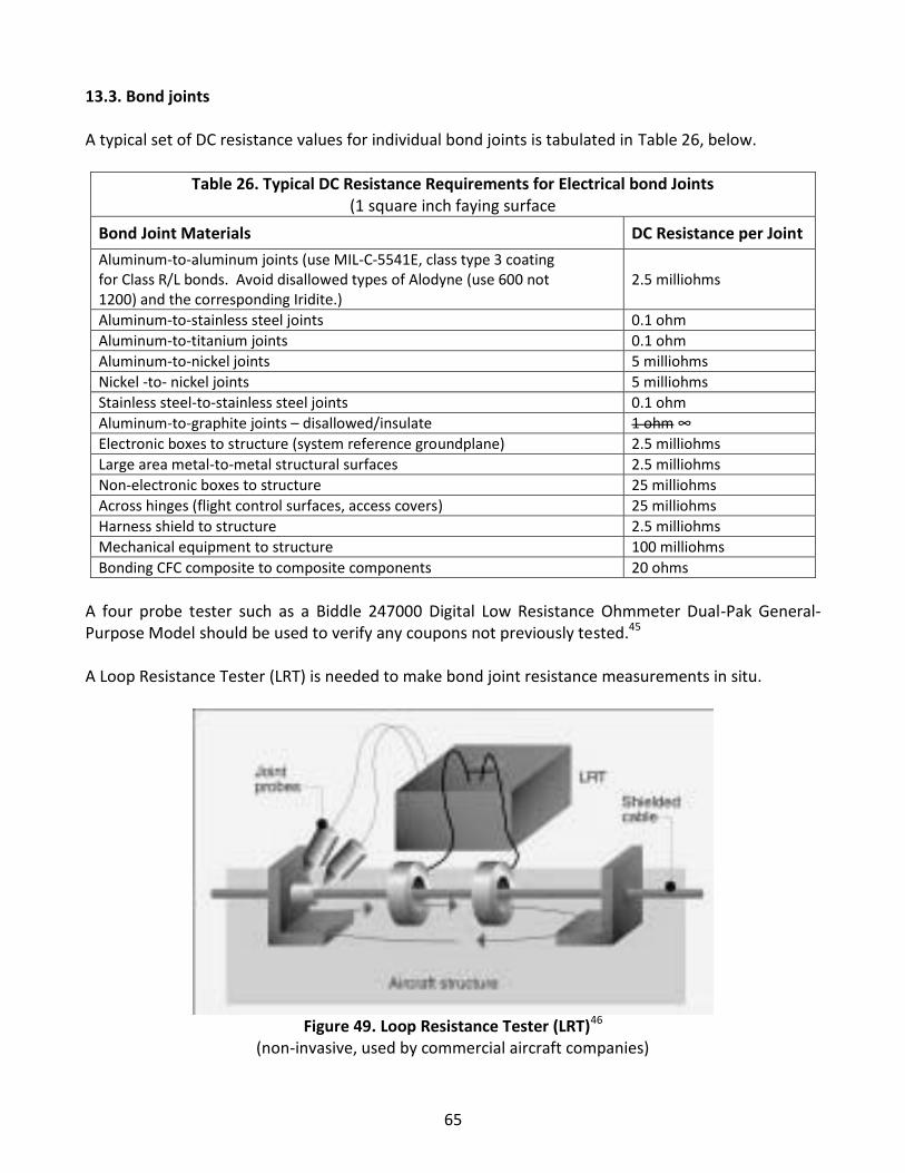
65
13.3. Bond joints
A typical set of DC resistance values for individual bond joints is tabulated in Table 26, below.
Table 26. Typical DC Resistance Requirements for Electrical bond Joints(1 square inch faying surface
Bond Joint Materials DC Resistance per Joint
Aluminum-to-aluminum joints (use MIL-C-5541E, class type 3 coatingfor Class R/L bonds. Avoid disallowed types of Alodyne (use 600 not1200) and the corresponding Iridite.)
2.5 milliohms
Aluminum-to-stainless steel joints 0.1 ohmAluminum-to-titanium joints 0.1 ohmAluminum-to-nickel joints 5 milliohmsNickel -to- nickel joints 5 milliohmsStainless steel-to-stainless steel joints 0.1 ohmAluminum-to-graphite joints – disallowed/insulate 1 ohm ∞Electronic boxes to structure (system reference groundplane) 2.5 milliohmsLarge area metal-to-metal structural surfaces 2.5 milliohmsNon-electronic boxes to structure 25 milliohmsAcross hinges (flight control surfaces, access covers) 25 milliohmsHarness shield to structure 2.5 milliohmsMechanical equipment to structure 100 milliohmsBonding CFC composite to composite components 20 ohms
A four probe tester such as a Biddle 247000 Digital Low Resistance Ohmmeter Dual-Pak General-Purpose Model should be used to verify any coupons not previously tested.45
A Loop Resistance Tester (LRT) is needed to make bond joint resistance measurements in situ.
Figure 49. Loop Resistance Tester (LRT)46
(non-invasive, used by commercial aircraft companies)
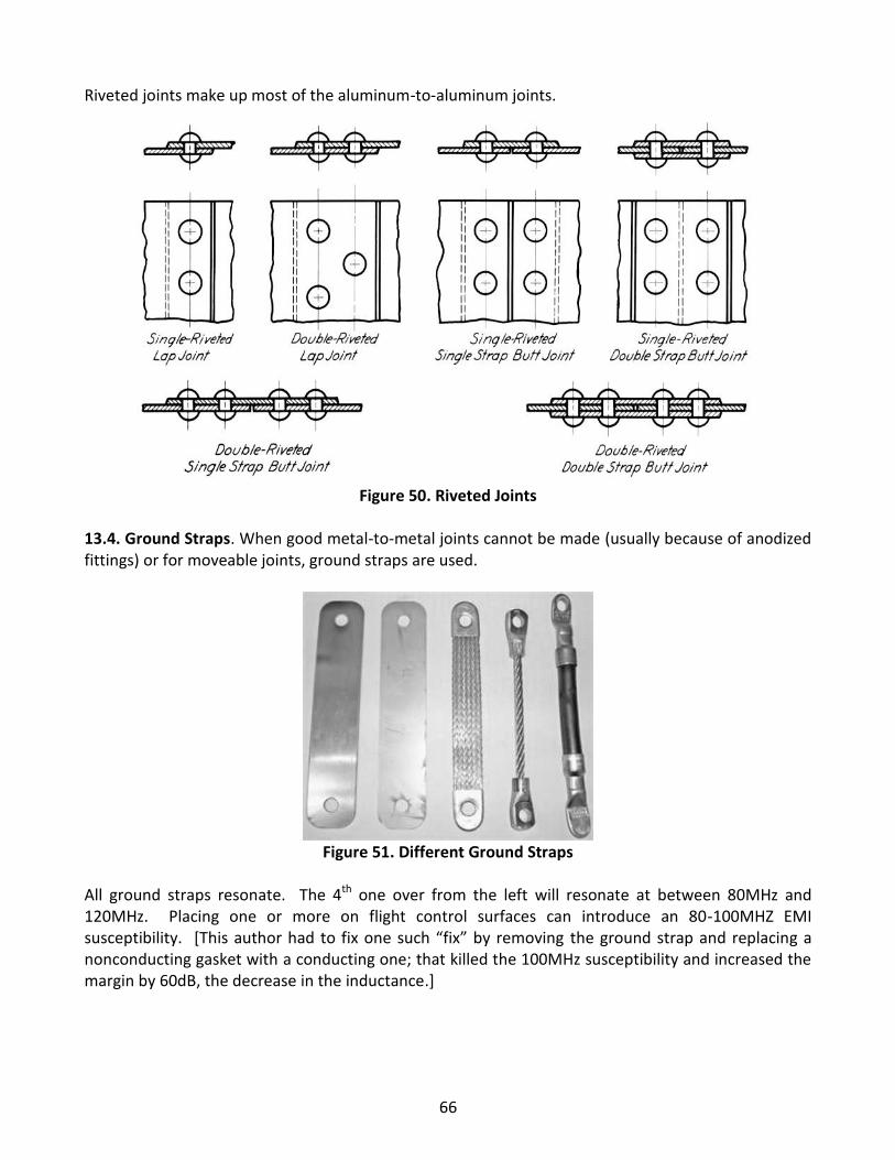
66
Riveted joints make up most of the aluminum-to-aluminum joints.
Figure 50. Riveted Joints
13.4. Ground Straps. When good metal-to-metal joints cannot be made (usually because of anodizedfittings) or for moveable joints, ground straps are used.
Figure 51. Different Ground Straps
All ground straps resonate. The 4th one over from the left will resonate at between 80MHz and120MHz. Placing one or more on flight control surfaces can introduce an 80-100MHZ EMIsusceptibility. [This author had to fix one such “fix” by removing the ground strap and replacing anonconducting gasket with a conducting one; that killed the 100MHz susceptibility and increased themargin by 60dB, the decrease in the inductance.]
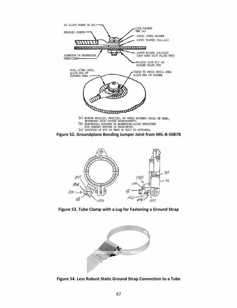
67
Figure 52. Groundplane Bonding Jumper Joint from MIL-B-5087B
Figure 53. Tube Clamp with a Lug for Fastening a Ground Strap
Figure 54. Less Robust Static Ground Strap Connection to a Tube
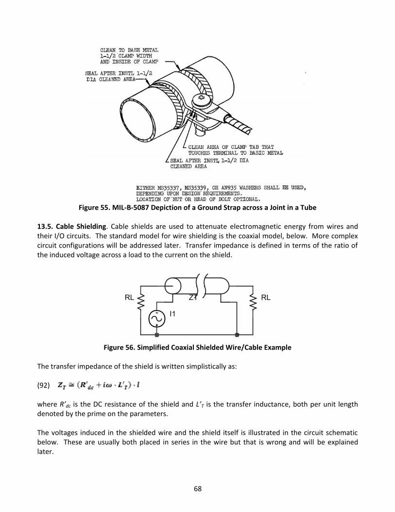
68
Figure 55. MIL-B-5087 Depiction of a Ground Strap across a Joint in a Tube
13.5. Cable Shielding. Cable shields are used to attenuate electromagnetic energy from wires andtheir I/O circuits. The standard model for wire shielding is the coaxial model, below. More complexcircuit configurations will be addressed later. Transfer impedance is defined in terms of the ratio ofthe induced voltage across a load to the current on the shield.
I1
ZTRL RL
Figure 56. Simplified Coaxial Shielded Wire/Cable Example
The transfer impedance of the shield is written simplistically as:
(92)
where R’dc is the DC resistance of the shield and L’T is the transfer inductance, both per unit lengthdenoted by the prime on the parameters.
The voltages induced in the shielded wire and the shield itself is illustrated in the circuit schematicbelow. These are usually both placed in series in the wire but that is wrong and will be explainedlater.
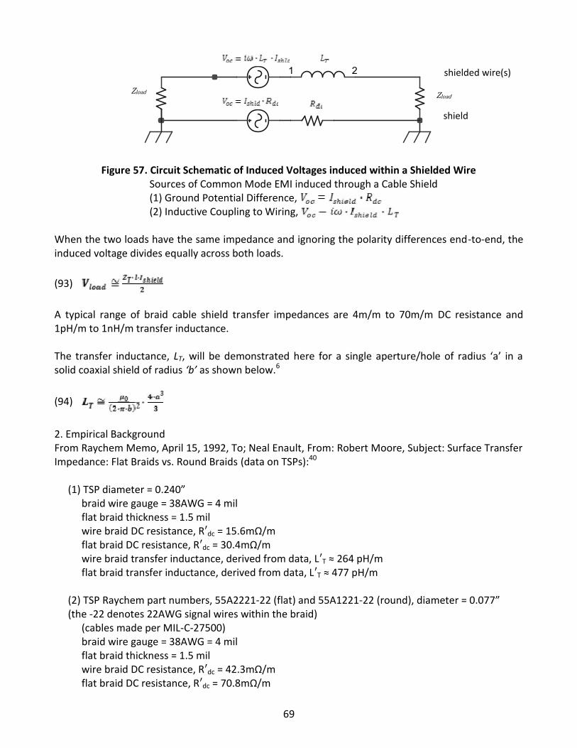
69
Voc=iwLI LT1 2
RdcVoc=IRRLRL
Figure 57. Circuit Schematic of Induced Voltages induced within a Shielded WireSources of Common Mode EMI induced through a Cable Shield(1) Ground Potential Difference,(2) Inductive Coupling to Wiring,
When the two loads have the same impedance and ignoring the polarity differences end-to-end, theinduced voltage divides equally across both loads.
(93)
A typical range of braid cable shield transfer impedances are 4m/m to 70m/m DC resistance and1pH/m to 1nH/m transfer inductance.
The transfer inductance, LT, will be demonstrated here for a single aperture/hole of radius ‘a’ in asolid coaxial shield of radius ‘b’ as shown below.6
(94)
2. Empirical BackgroundFrom Raychem Memo, April 15, 1992, To; Neal Enault, From: Robert Moore, Subject: Surface TransferImpedance: Flat Braids vs. Round Braids (data on TSPs):40
(1) TSP diameter = 0.240”braid wire gauge = 38AWG = 4 milflat braid thickness = 1.5 milwire braid DC resistance, R′dc = 15.6mΩ/mflat braid DC resistance, R′dc = 30.4mΩ/mwire braid transfer inductance, derived from data, L′T ≈ 264 pH/mflat braid transfer inductance, derived from data, L′T ≈ 477 pH/m
(2) TSP Raychem part numbers, 55A2221-22 (flat) and 55A1221-22 (round), diameter = 0.077”(the -22 denotes 22AWG signal wires within the braid)
(cables made per MIL-C-27500)braid wire gauge = 38AWG = 4 milflat braid thickness = 1.5 milwire braid DC resistance, R′dc = 42.3mΩ/mflat braid DC resistance, R′dc = 70.8mΩ/m
shielded wire(s)
shield
ZloadZload Zload
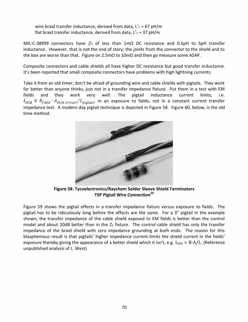
70
wire braid transfer inductance, derived from data, L′T ≈ 67 pH/mflat braid transfer inductance, derived from data, L′T ≈ 37 pH/m
MIL-C-38999 connectors have ZT of less than 1mΩ DC resistance and 0.5pH to 5pH transferinductance. However, that is not the end of story; the joints from the connector to the shield and tothe box are worse than that. Figure on 2.5mΩ to 10mΩ and then go measure some ASAP.
Composite connectors and cable shields all have higher DC resistance but good transfer inductance.It’s been reported that small composite connectors have problems with high lightning currents.
Take it from an old timer; don’t be afraid of grounding wire and cable shields with pigtails. They workfar better than anyone thinks, just not in a transfer impedance fixture. Put them in a test with EMfields and they work very well. The pigtail inductance current limits, i.e.
, in an exposure to fields, not in a constant current transferimpedance test. A modern day pigtail technique is depicted in Figure 58. Figure 60, below, is the oldtime method.
Figure 58. Tycoelectronics/Raychem Solder Sleeve Shield TerminatorsTSP Pigtail Wire Connection59
Figure 59 shows the pigtail effects in a transfer impedance fixture versus exposure to fields. Thepigtail has to be ridiculously long before the effects are the same. For a 3” pigtail in the exampleshown, the transfer impedance of the cable shield exposed to EM fields is better than the controlmodel and about 20dB better than in the ZT fixture. The control cable shield has only the transferimpedance of the braid shield with zero impedance grounding at both ends. The reason for thisblasphemous result is that pigtails’ higher impedance current-limits the shield current in the fields’exposure thereby giving the appearance of a better shield which it isn’t, e.g. Ishld = B∙A/L. (Referenceunpublished analysis of L. West)
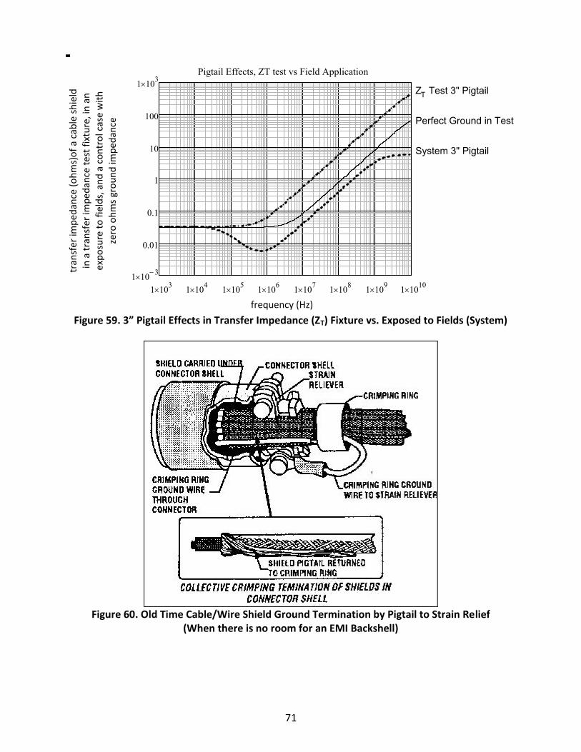
71
1 103 1 104 1 105 1 106 1 107 1 108 1 109 1 10101 10 3
0.01
0.1
1
10
100
1 103Pigtail Effects, ZT test vs Field Application
ZST n 3( )
ZFT n 3( )
ZST n 1( )
f n( )
ZT Test 3" Pigtail
Perfect Ground in Test
System 3" Pigtail
Figure 59. 3” Pigtail Effects in Transfer Impedance (ZT) Fixture vs. Exposed to Fields (System)
Figure 60. Old Time Cable/Wire Shield Ground Termination by Pigtail to Strain Relief(When there is no room for an EMI Backshell)
tran
sfer
impe
danc
e(o
hms)
of a
cab
le s
hiel
din
a tr
ansf
er im
peda
nce
test
fixt
ure,
inan
expo
sure
to fi
elds
, and
a c
ontr
ol c
ase
with
zero
ohm
s gr
ound
impe
danc
e
frequency (Hz)
72
13.6. Cable Separation. Isolation through cable separation is necessary to keep high current cablesfrom inducing noise into low voltage cables. With cables of length, l, a distance, d, apart and aheight, h, above a groundplane, the mutual coupling is
(95) with the cable radius, r, included and
(96) with the cable radius, r, set to zero.
Mutual coupling of WF4 currents into WH1 currents and WF2 voltages in adjacent cables is depictedin Figures 34 and 35.
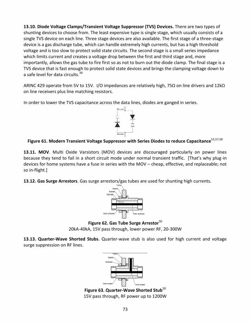
73
13.10. Diode Voltage Clamps/Transient Voltage Suppressor (TVS) Devices. There are two types ofshunting devices to choose from. The least expensive type is single stage, which usually consists of asingle TVS device on each line. Three stage devices are also available. The first stage of a three-stagedevice is a gas discharge tube, which can handle extremely high currents, but has a high thresholdvoltage and is too slow to protect solid state circuits. The second stage is a small series impedancewhich limits current and creates a voltage drop between the first and third stage and, moreimportantly, allows the gas tube to fire first so as not to burn out the diode clamp. The final stage is aTVS device that is fast enough to protect solid state devices and brings the clamping voltage down toa safe level for data circuits.39
ARINC 429 operate from 5V to 15V. I/O impedances are relatively high, 75Ω on line drivers and 12kΩon line receivers plus line matching resistors.
In order to lower the TVS capacitance across the data lines, diodes are ganged in series.
Figure 61. Modern Transient Voltage Suppressor with Series Diodes to reduce Capacitance53,57,58
13.11. MOV. Multi Oxide Varsistors (MOV) devices are discouraged particularly on power linesbecause they tend to fail in a short circuit mode under normal transient traffic. [That’s why plug-indevices for home systems have a fuse in series with the MOV – cheap, effective, and replaceable; notso in-flight.]
13.12. Gas Surge Arrestors. Gas surge arrestors/gas tubes are used for shunting high currents.
Figure 62. Gas Tube Surge Arrestor50
20kA-40kA, 15V pass through, lower power RF, 20-300W
13.13. Quarter-Wave Shorted Stubs. Quarter-wave stub is also used for high current and voltagesurge suppression on RF lines.
Figure 63. Quarter-Wave Shorted Stub50
15V pass through, RF power up to 1200W
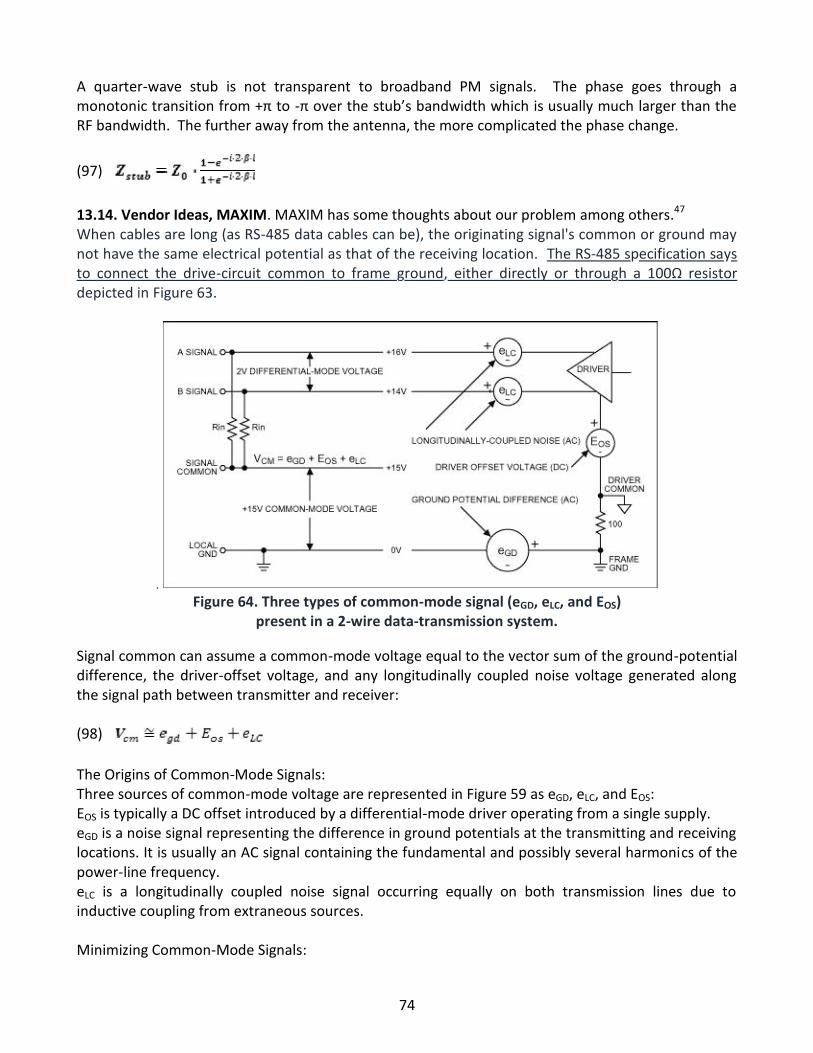
74
A quarter-wave stub is not transparent to broadband PM signals. The phase goes through amonotonic transition from +π to -π over the stub’s bandwidth which is usually much larger than theRF bandwidth. The further away from the antenna, the more complicated the phase change.
(97)
13.14. Vendor Ideas, MAXIM. MAXIM has some thoughts about our problem among others.47
When cables are long (as RS-485 data cables can be), the originating signal's common or ground maynot have the same electrical potential as that of the receiving location. The RS-485 specification saysto connect the drive-circuit common to frame ground, either directly or through a 100Ω resistordepicted in Figure 63.
.Figure 64. Three types of common-mode signal (eGD, eLC, and EOS)
present in a 2-wire data-transmission system.
Signal common can assume a common-mode voltage equal to the vector sum of the ground-potentialdifference, the driver-offset voltage, and any longitudinally coupled noise voltage generated alongthe signal path between transmitter and receiver:
(98)
The Origins of Common-Mode Signals:Three sources of common-mode voltage are represented in Figure 59 as eGD, eLC, and EOS:EOS is typically a DC offset introduced by a differential-mode driver operating from a single supply.eGD is a noise signal representing the difference in ground potentials at the transmitting and receivinglocations. It is usually an AC signal containing the fundamental and possibly several harmonics of thepower-line frequency.eLC is a longitudinally coupled noise signal occurring equally on both transmission lines due toinductive coupling from extraneous sources.
Minimizing Common-Mode Signals:
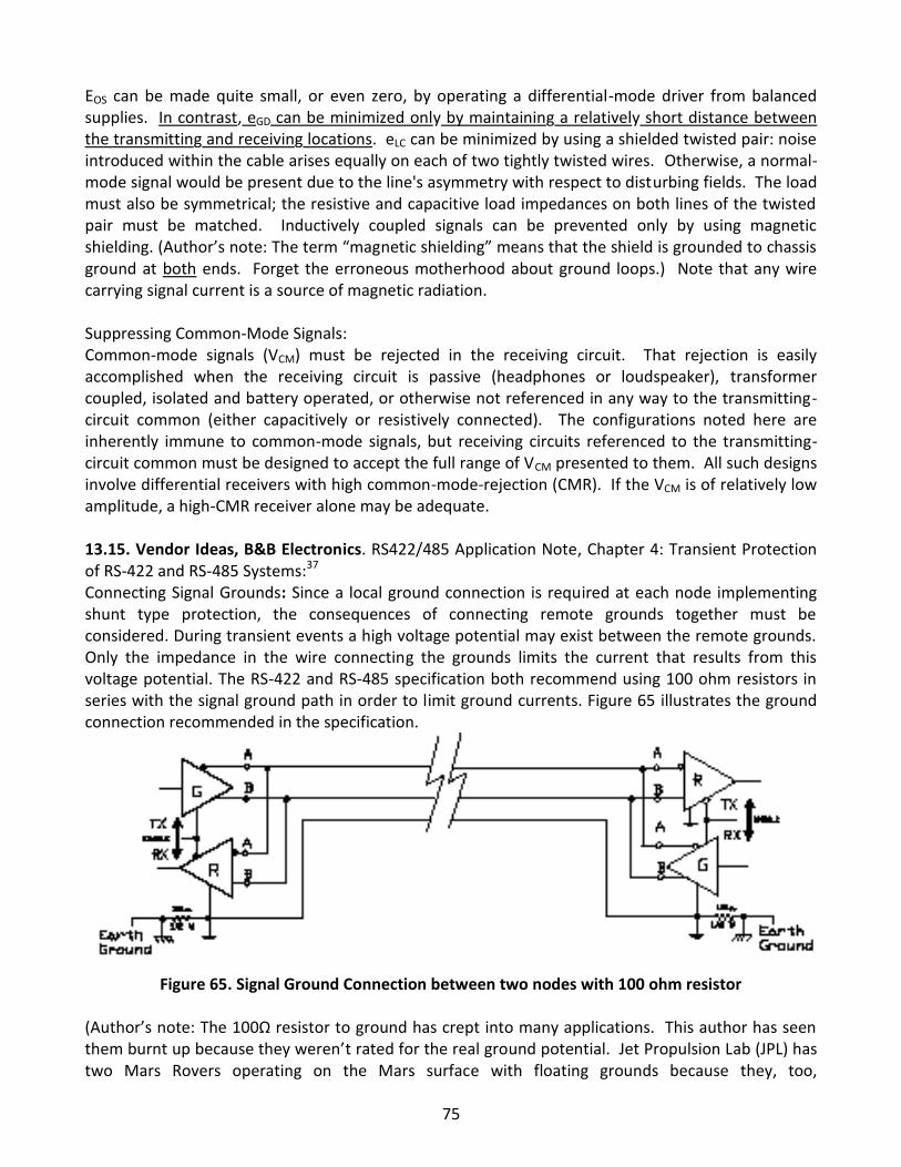
75
EOS can be made quite small, or even zero, by operating a differential-mode driver from balancedsupplies. In contrast, eGD can be minimized only by maintaining a relatively short distance betweenthe transmitting and receiving locations. eLC can be minimized by using a shielded twisted pair: noiseintroduced within the cable arises equally on each of two tightly twisted wires. Otherwise, a normal-mode signal would be present due to the line's asymmetry with respect to disturbing fields. The loadmust also be symmetrical; the resistive and capacitive load impedances on both lines of the twistedpair must be matched. Inductively coupled signals can be prevented only by using magneticshielding. (Author’s note: The term “magnetic shielding” means that the shield is grounded to chassisground at both ends. Forget the erroneous motherhood about ground loops.) Note that any wirecarrying signal current is a source of magnetic radiation.
Suppressing Common-Mode Signals:Common-mode signals (VCM) must be rejected in the receiving circuit. That rejection is easilyaccomplished when the receiving circuit is passive (headphones or loudspeaker), transformercoupled, isolated and battery operated, or otherwise not referenced in any way to the transmitting-circuit common (either capacitively or resistively connected). The configurations noted here areinherently immune to common-mode signals, but receiving circuits referenced to the transmitting-circuit common must be designed to accept the full range of VCM presented to them. All such designsinvolve differential receivers with high common-mode-rejection (CMR). If the VCM is of relatively lowamplitude, a high-CMR receiver alone may be adequate.
13.15. Vendor Ideas, B&B Electronics. RS422/485 Application Note, Chapter 4: Transient Protectionof RS-422 and RS-485 Systems:37
Connecting Signal Grounds: Since a local ground connection is required at each node implementingshunt type protection, the consequences of connecting remote grounds together must beconsidered. During transient events a high voltage potential may exist between the remote grounds.Only the impedance in the wire connecting the grounds limits the current that results from thisvoltage potential. The RS-422 and RS-485 specification both recommend using 100 ohm resistors inseries with the signal ground path in order to limit ground currents. Figure 65 illustrates the groundconnection recommended in the specification.
Figure 65. Signal Ground Connection between two nodes with 100 ohm resistor
(Author’s note: The 100Ω resistor to ground has crept into many applications. This author has seenthem burnt up because they weren’t rated for the real ground potential. Jet Propulsion Lab (JPL) hastwo Mars Rovers operating on the Mars surface with floating grounds because they, too,
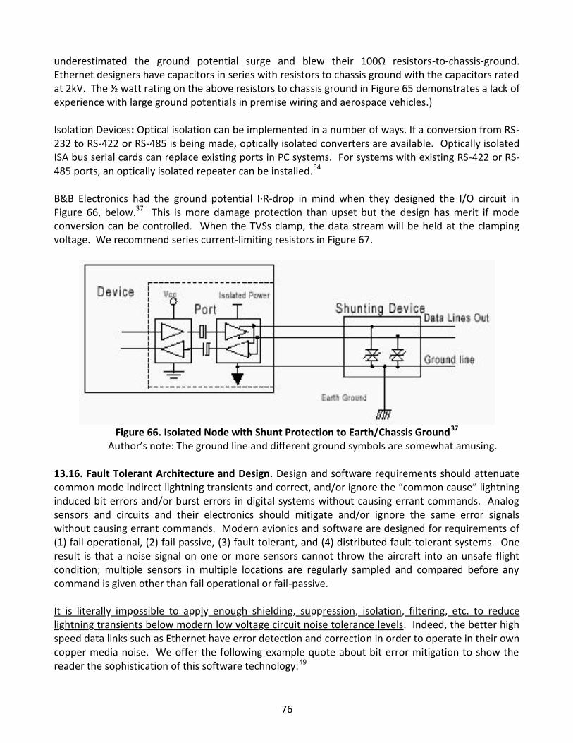
76
underestimated the ground potential surge and blew their 100Ω resistors-to-chassis-ground.Ethernet designers have capacitors in series with resistors to chassis ground with the capacitors ratedat 2kV. The ½ watt rating on the above resistors to chassis ground in Figure 65 demonstrates a lack ofexperience with large ground potentials in premise wiring and aerospace vehicles.)
Isolation Devices: Optical isolation can be implemented in a number of ways. If a conversion from RS-232 to RS-422 or RS-485 is being made, optically isolated converters are available. Optically isolatedISA bus serial cards can replace existing ports in PC systems. For systems with existing RS-422 or RS-485 ports, an optically isolated repeater can be installed.54
B&B Electronics had the ground potential I∙R-drop in mind when they designed the I/O circuit inFigure 66, below.37 This is more damage protection than upset but the design has merit if modeconversion can be controlled. When the TVSs clamp, the data stream will be held at the clampingvoltage. We recommend series current-limiting resistors in Figure 67.
Figure 66. Isolated Node with Shunt Protection to Earth/Chassis Ground37
Author’s note: The ground line and different ground symbols are somewhat amusing.
13.16. Fault Tolerant Architecture and Design. Design and software requirements should attenuatecommon mode indirect lightning transients and correct, and/or ignore the “common cause” lightninginduced bit errors and/or burst errors in digital systems without causing errant commands. Analogsensors and circuits and their electronics should mitigate and/or ignore the same error signalswithout causing errant commands. Modern avionics and software are designed for requirements of(1) fail operational, (2) fail passive, (3) fault tolerant, and (4) distributed fault-tolerant systems. Oneresult is that a noise signal on one or more sensors cannot throw the aircraft into an unsafe flightcondition; multiple sensors in multiple locations are regularly sampled and compared before anycommand is given other than fail operational or fail-passive.
It is literally impossible to apply enough shielding, suppression, isolation, filtering, etc. to reducelightning transients below modern low voltage circuit noise tolerance levels. Indeed, the better highspeed data links such as Ethernet have error detection and correction in order to operate in their owncopper media noise. We offer the following example quote about bit error mitigation to show thereader the sophistication of this software technology:49
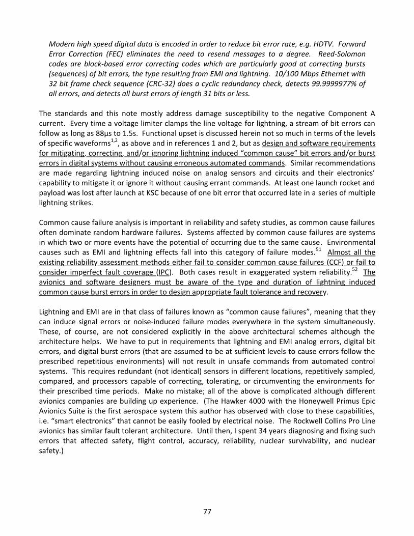
77
Modern high speed digital data is encoded in order to reduce bit error rate, e.g. HDTV. ForwardError Correction (FEC) eliminates the need to resend messages to a degree. Reed-Solomoncodes are block-based error correcting codes which are particularly good at correcting bursts(sequences) of bit errors, the type resulting from EMI and lightning. 10/100 Mbps Ethernet with32 bit frame check sequence (CRC-32) does a cyclic redundancy check, detects 99.9999977% ofall errors, and detects all burst errors of length 31 bits or less.
The standards and this note mostly address damage susceptibility to the negative Component Acurrent. Every time a voltage limiter clamps the line voltage for lightning, a stream of bit errors canfollow as long as 88µs to 1.5s. Functional upset is discussed herein not so much in terms of the levelsof specific waveforms1,2, as above and in references 1 and 2, but as design and software requirementsfor mitigating, correcting, and/or ignoring lightning induced “common cause” bit errors and/or bursterrors in digital systems without causing erroneous automated commands. Similar recommendationsare made regarding lightning induced noise on analog sensors and circuits and their electronics’capability to mitigate it or ignore it without causing errant commands. At least one launch rocket andpayload was lost after launch at KSC because of one bit error that occurred late in a series of multiplelightning strikes.
Common cause failure analysis is important in reliability and safety studies, as common cause failuresoften dominate random hardware failures. Systems affected by common cause failures are systemsin which two or more events have the potential of occurring due to the same cause. Environmentalcauses such as EMI and lightning effects fall into this category of failure modes.51 Almost all theexisting reliability assessment methods either fail to consider common cause failures (CCF) or fail toconsider imperfect fault coverage (IPC). Both cases result in exaggerated system reliability.52 Theavionics and software designers must be aware of the type and duration of lightning inducedcommon cause burst errors in order to design appropriate fault tolerance and recovery.
Lightning and EMI are in that class of failures known as “common cause failures”, meaning that theycan induce signal errors or noise-induced failure modes everywhere in the system simultaneously.These, of course, are not considered explicitly in the above architectural schemes although thearchitecture helps. We have to put in requirements that lightning and EMI analog errors, digital biterrors, and digital burst errors (that are assumed to be at sufficient levels to cause errors follow theprescribed repetitious environments) will not result in unsafe commands from automated controlsystems. This requires redundant (not identical) sensors in different locations, repetitively sampled,compared, and processors capable of correcting, tolerating, or circumventing the environments fortheir prescribed time periods. Make no mistake; all of the above is complicated although differentavionics companies are building up experience. (The Hawker 4000 with the Honeywell Primus EpicAvionics Suite is the first aerospace system this author has observed with close to these capabilities,i.e. “smart electronics” that cannot be easily fooled by electrical noise. The Rockwell Collins Pro Lineavionics has similar fault tolerant architecture. Until then, I spent 34 years diagnosing and fixing sucherrors that affected safety, flight control, accuracy, reliability, nuclear survivability, and nuclearsafety.)
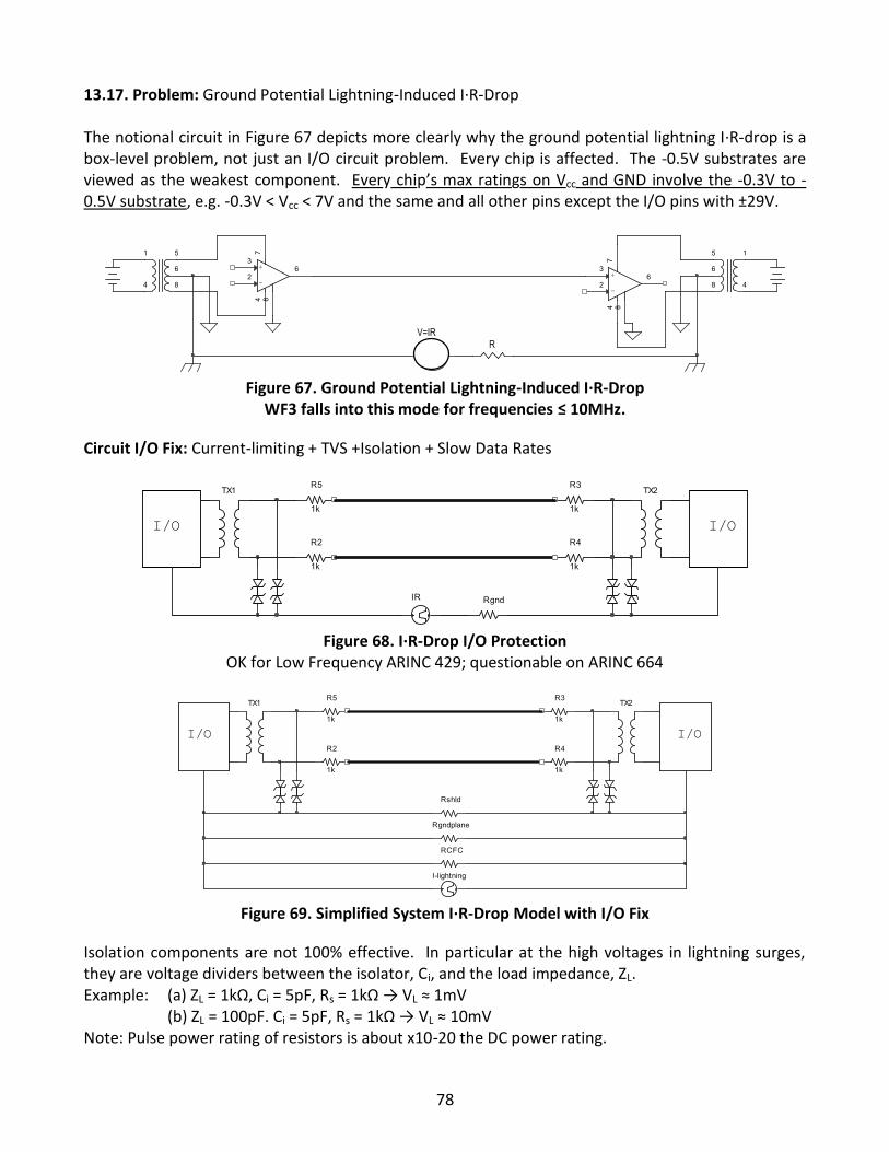
78
13.17. Problem: Ground Potential Lightning-Induced I∙R-Drop
The notional circuit in Figure 67 depicts more clearly why the ground potential lightning I∙R-drop is abox-level problem, not just an I/O circuit problem. Every chip is affected. The -0.5V substrates areviewed as the weakest component. Every chip’s max ratings on Vcc and GND involve the -0.3V to -0.5V substrate, e.g. -0.3V < Vcc < 7V and the same and all other pins except the I/O pins with ±29V.
-
+2
67
34 8
-
+2
6
7
3
4 8
R
1 5
6
4 8
15
6
48
V=IR
Figure 67. Ground Potential Lightning-Induced I∙R-DropWF3 falls into this mode for frequencies ≤ 10MHz.
Circuit I/O Fix: Current-limiting + TVS +Isolation + Slow Data Rates
Rgnd
I/O
TX1
R2
1k
TX2R5
1k
R3
1k
IR
R4
1k
I/O
Figure 68. I∙R-Drop I/O ProtectionOK for Low Frequency ARINC 429; questionable on ARINC 664
Rshld
I/O
TX1
R2
1k
TX2
I-lightning
R5
1k
R3
1k
R4
1k
I/O
RCFC
Rgndplane
Figure 69. Simplified System I∙R-Drop Model with I/O Fix
Isolation components are not 100% effective. In particular at the high voltages in lightning surges,they are voltage dividers between the isolator, Ci, and the load impedance, ZL.Example: (a) ZL = 1kΩ, Ci = 5pF, Rs = 1kΩ → VL ≈ 1mV
(b) ZL = 100pF. Ci = 5pF, Rs = 1kΩ → VL ≈ 10mVNote: Pulse power rating of resistors is about x10-20 the DC power rating.
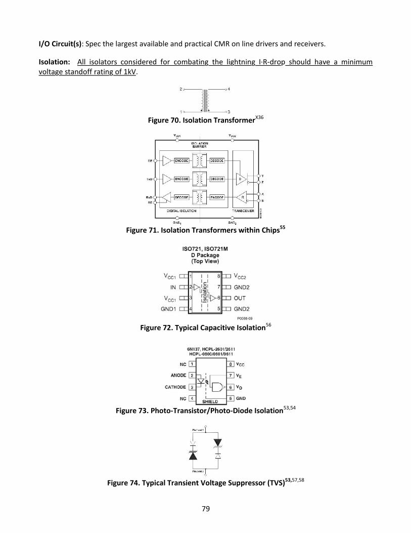
79
I/O Circuit(s): Spec the largest available and practical CMR on line drivers and receivers.
Isolation: All isolators considered for combating the lightning I∙R-drop should have a minimumvoltage standoff rating of 1kV.
Figure 70. Isolation TransformerX36
Figure 71. Isolation Transformers within Chips55
Figure 72. Typical Capacitive Isolation56
Figure 73. Photo-Transistor/Photo-Diode Isolation53,54
Figure 74. Typical Transient Voltage Suppressor (TVS)53,57,58
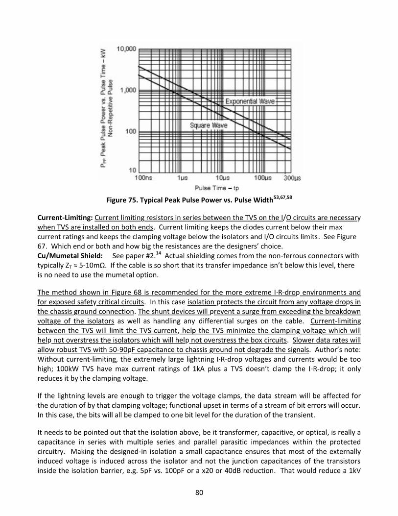
80
Figure 75. Typical Peak Pulse Power vs. Pulse Width53,67,58
Current-Limiting: Current limiting resistors in series between the TVS on the I/O circuits are necessarywhen TVS are installed on both ends. Current limiting keeps the diodes current below their maxcurrent ratings and keeps the clamping voltage below the isolators and I/O circuits limits. See Figure67. Which end or both and how big the resistances are the designers’ choice.Cu/Mumetal Shield: See paper #2.14 Actual shielding comes from the non-ferrous connectors withtypically ZT ≈ 5-10mΩ. If the cable is so short that its transfer impedance isn’t below this level, thereis no need to use the mumetal option.
The method shown in Figure 68 is recommended for the more extreme I∙R-drop environments andfor exposed safety critical circuits. In this case isolation protects the circuit from any voltage drops inthe chassis ground connection. The shunt devices will prevent a surge from exceeding the breakdownvoltage of the isolators as well as handling any differential surges on the cable. Current-limitingbetween the TVS will limit the TVS current, help the TVS minimize the clamping voltage which willhelp not overstress the isolators which will help not overstress the box circuits. Slower data rates willallow robust TVS with 50-90pF capacitance to chassis ground not degrade the signals. Author’s note:Without current-limiting, the extremely large lightning I∙R-drop voltages and currents would be toohigh; 100kW TVS have max current ratings of 1kA plus a TVS doesn’t clamp the I∙R-drop; it onlyreduces it by the clamping voltage.
If the lightning levels are enough to trigger the voltage clamps, the data stream will be affected forthe duration of by that clamping voltage; functional upset in terms of a stream of bit errors will occur.In this case, the bits will all be clamped to one bit level for the duration of the transient.
It needs to be pointed out that the isolation above, be it transformer, capacitive, or optical, is really acapacitance in series with multiple series and parallel parasitic impedances within the protectedcircuitry. Making the designed-in isolation a small capacitance ensures that most of the externallyinduced voltage is induced across the isolator and not the junction capacitances of the transistorsinside the isolation barrier, e.g. 5pF vs. 100pF or a x20 or 40dB reduction. That would reduce a 1kV
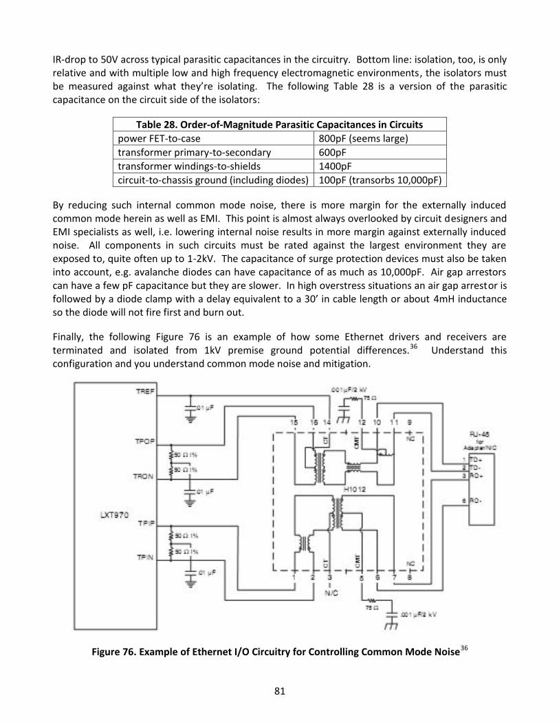
81
IR-drop to 50V across typical parasitic capacitances in the circuitry. Bottom line: isolation, too, is onlyrelative and with multiple low and high frequency electromagnetic environments, the isolators mustbe measured against what they’re isolating. The following Table 28 is a version of the parasiticcapacitance on the circuit side of the isolators:
Table 28. Order-of-Magnitude Parasitic Capacitances in Circuitspower FET-to-case 800pF (seems large)transformer primary-to-secondary 600pFtransformer windings-to-shields 1400pFcircuit-to-chassis ground (including diodes) 100pF (transorbs 10,000pF)
By reducing such internal common mode noise, there is more margin for the externally inducedcommon mode herein as well as EMI. This point is almost always overlooked by circuit designers andEMI specialists as well, i.e. lowering internal noise results in more margin against externally inducednoise. All components in such circuits must be rated against the largest environment they areexposed to, quite often up to 1-2kV. The capacitance of surge protection devices must also be takeninto account, e.g. avalanche diodes can have capacitance of as much as 10,000pF. Air gap arrestorscan have a few pF capacitance but they are slower. In high overstress situations an air gap arrestor isfollowed by a diode clamp with a delay equivalent to a 30’ in cable length or about 4mH inductanceso the diode will not fire first and burn out.
Finally, the following Figure 76 is an example of how some Ethernet drivers and receivers areterminated and isolated from 1kV premise ground potential differences.36 Understand thisconfiguration and you understand common mode noise and mitigation.
Figure 76. Example of Ethernet I/O Circuitry for Controlling Common Mode Noise36
82
Note the 2kV voltage rating of the common mode DC isolation/AC termination capacitors. This isbecause the ends of the Ethernet cables terminate in boxes powered from different power mainswith different grounding. The result is large ground potential differences that themselves can wreakhavoc with the electronics.
These circuits represent the ultimate in mitigation of common mode problems with circuit design.And, yet, software mitigation is necessary to lower the bit error rate. When TVS clamp, the bit errorsand burst errors can last as long as 88µs to 1.5ms. Signal mode noise thresholds are around 100mVand CMR ranges from -0.5V to ±30V depending upon chip design.
As good as ±7V sounds to a designer in a benign environment, ±7V is a low threshold for lightning I∙R-drop. That tells us how much we must suppress the lightning induced IR-drop for RS-422 circuits.The above I/O fix applied to one wire only drops the voltage across the loads to 1-10mV. Theproblem is that the power dissipated in the current-limiting resistors is large but the pulse rating isabout x10-20 the DC power rating.
83
14. Concluding Remarks
1. Tables of transient levels in SAE ARP5412A and in DO-160F are totally misleading. In the hands ofuntrained engineers, the environments chosen are usually ludicrous. The levels of protectionbetween the largest and smallest allocations are fictitious. The total lack of guidance and simplealgorithms for the system designers is appalling.
2. This note, while not all inclusive, provides the lightning engineer with simple model formulas forallocating reasonable waveforms and levels early in a system program. Circuit designers must beeducated about the common mode nature of the lightning and EMI environments at their I/O circuits.
3. The most important allocations early in a program are cable shields, I/O circuit protection,groundplane parameters, and bond joints’ resistances. These all add weight and space that weightconscious manager’s hate, i.e. their weight bogies were made up before you showed up. Thesefeatures can be 100% tested or inspected on every tail number and form the basis for certificates ofindirect lightning protection in production. The aircraft that undergoes system level lightning testingand the boxes that undergo lightning testing will provide a sample of safety margins and error budgetfor production tolerances. Similarity will provide the rest based upon theoretical models that canscale untested components to their anticipated safety margins. The system level test is an excellentsystem level in situ bond joint diagnostic tool and, in fact, that may be the real reason for running thetest but don’t advertise that kind of reality.
4. Environments have been scaled to in-flight interactions instead of ground-test.
5. Environment allocations have been scaled by system and cable geometry and electrical parametersinstead of one size fits all.
6. Lightning Components A, D, and H have the same dI/dt and have the same spectra above 2MHztherefore the same WF2 and WF3 induced transients.
7. The IR-drop induced voltage is proportional to the distance between boxes along the airframecurrent path; the induced cable current is independent of that distance. Induced voltage s throughcable shields is proportional the cable length. This is important for the power rating of surgesuppressors.
8. Levels of Protection have been shown to involve cable-to-cable mutual coupling not attenuation ofexternal fields. For purposes of standardization, the number of transient levels should increase onboth the low and high sides. The only controlled shielding is box and cable shielding therefore theonly shielding available for protection credit.
9. Induced environments are directly dependent upon parameters 100% inspectable and nearly 100%testable during airframe fabrication, a key to production certification by tail number.
10. Copper cable shielding with less than 30AWG thickness cannot attenuate low frequency WF1 andWF4 more than a few dB. The shielding is necessary for EMI and WF3 lightning.
84
11. Shielding and other physical protection cannot attenuate lightning induced noise below electronicnoise thresholds.
12. TVS components between I/O lines and chassis ground cannot clamp the I∙R-drop to TVS clampingvoltage without current-limiting; they can only reduce the I∙R-drop by the clamping voltage. Plus, a100kW 40VBD TVS has little over 1kA max current IPP rating and a 500W 12VBD TVS has IPP = 20A. For a1kA WF4 cable current, 50 12VBD parallel TVSs would have to fire simultaneously in order to notexceed these limits.
13. Functional upset criteria should include software mitigation of bit errors and burst errors theduration of the transients and disallow erroneous commands from automated flight controlelectronics due to 88µs to 1.5s of transient noise. Common-cause failure modes from EMI andlightning beg architecture for fail-operational, fail-passive, distributed fault tolerance, and faulttolerance and recovery in general.
14. Protection of electronics against the lightning induced I∙R-drop is considered to be high riskbecause of unknown susceptibilities. DO-160 ground injection tests have not been performedcorrectly. The I∙R-drop and ground injection have been considered an I/O circuit susceptibility. I/Ochip max ground potential ratings seldom exceed tens of volts including transformer isolated MIL-STD-1553. All chip max ratings other than I/O input/output pins are based upon substrate biases ofless than negative one volt.
15. Isolation rated for ≥ 1kV installed in the I/O circuitry is required for the extreme I∙R-dropenvironments. Isolation installed in series with I/O circuits is relative, not 100%. In terms of lowfrequency lightning transients, isolation is a capacitive voltage divider the success of which dependsupon the impedance to chassis ground within the protected electronics in series with the isolator(s).
16. Indirect lightning protection has been broken down into the following:
a) Groundplane resistance,b) Cable shield resistance,c) Bond joint resistance,d) TVS common mode protection,e) Current-limiting,f) Isolation between the TVS and the box I/O circuits including the possibility of isolated powersupplies,g) Combined copper and mumetal cable shields (limited by the shielding of the non-ferrousconnectors),h) Software fault tolerance of common-cause transient burst errors and recovery afterwards, andi) Slower data rates like ARINC 429 allow 50-90pF TVS pin-to-chassis.
17. Engineering tests are needed throughout to establish parameters and tweak designs.
85
References
1. Radio Technical Committee on Aeronautics, RTCA/DO-160F, “Environmental Conditions and TestProcedures for Airborne Equipment, Section 22, Lightning Induced Transient Susceptibility”, Dec 2007
2. Society of Automotive Engineers Aerospace Recommended Practices, SAE ARP5412A, “AircraftLightning Environment and Related Test Waveforms”, Revised 2005-02
3. SAE ARP 5415A, “User’s Manual for Certification of Aircraft Electrical/Electronic Systems for theIndirect Effects of Lightning”, Revised 2002-04
4. FAA Advisory Circular on HIRF, AC 21-16C, 2/14/1990
5. FAA Advisory Circular on Indirect Lightning, AC 20-136A, 12/21/2006
6. Lee, K. S. H., Editor, EMP Interaction: Principles, Techniques, and Reference Data, Taylor & Francis,NY, 1995, a summary reference book based mostly on the Note Series of Carl E. Baum found onhttp://www.ece.unm.edu/summa/notes/index.html
7. Schelkunoff, S. A., “The Electromagnetic Theory of Coaxial Transmission Lines and CylindricalShields”, The Bell System Technical Journal, Volume XIII, 1934, 532-579
8. Meriwether, Cooper, & Parker, Electromagnetic Pulse Handbook for Missiles and Aircraft in Flight,EMP Interaction 1-1, Sandia Laboratories, 1968 (Prepared for AFWL)
9. Ramo, Whinnery, & Van Duzer, Fields and Waves in Communication Electronics, 3rd Edition, JohnWiley & Sons, NY, 1994
10. Goldman, Stanford, Laplace Transform Theory and Electrical Transients, Dover Publications, Inc.,NY, 1966 (copyright 1949)
11. Vance, E. F., Coupling to Shielded Cables, Wiley, NY, 1978
12. Vance, E. F., “Comparison of Electric and Magnetic Coupling through Braided-Wire Shields”, SRITechnical Memorandum 18, February, 1972 (Prepared for AFWL)
13. West, Larry, “In-Flight vs. Ground-Test Lightning Interactions in Composite Airframes, Effects ofExternal vs. Internal inductance, An Errata to Everything Previously Published,” IN615, April 2011
14. West, Larry, Interaction Note 608, “Lightning Induced Waveform 5 in Composite Airframes, theInability of Copper Braid to Shield It, and A New Layered Copper Braid and High-mu Foil Shield”,February 2009, www.ece.unm.edu/summa/notes/In/0608.pdf, Rev A, IN616, April 2011
15. West, Larry, IN618, “Assessment of & Recommendations for RTCA/DO-160F Section 22 LightningInduced Transient Susceptibility”, September 2010
86
16. Casey, K. F., “Electromagnetic Shielding by Advanced Composite Materials”, Interaction Note 341,June 1977
17. West, Larry, Invited presentation to IEEE Region 5 Galveston Bay Section EMC Chapter MeetingWednesday September 22, 2010, “Lightning Induced Transients in Composite Airframes - Analysis,Design, & Test”
18. Baum, Carl E., “Parameters for Some Electrically-Small Electromagnetic Sensors”, Sensor andSimulation Note 38, 21 Mar 67, Air Force Weapons Laboratory
19. Baum, C. E., “Electromagnetic Pulse Interaction Close to Nuclear Bursts and Associated EMPEnvironment Specification”, Interaction Note 76, 2 Jul 71, Air Force Weapons Laboratory
20. MIL-STD-285, Notice 1, “Attenuation Measurements for Enclosures, Electromagnetic Shielding, forElectronic Test Purposes, Method of”, 24 October 1997
21. Ogunsola, Ade, “Harmonization of Shielding-Effectiveness Standards for Enclosures”,http://www.ce-mag.com/archive/01/Spring/Ogunsola.html
22. Carter, Nigel, “The Background to the HIRF Requirements for Civil Aerospace”, ComplianceMagazine, http://www.compliance-club.com/archive/old_archive/980212.html
23. Kajfez, D., “Excitation of a Terminated TEM Transmission Line through a Small Aperture”,Interaction Note 215, Jul 74, University of Mississippi, AFWL-TR-74-195, AD A021488
24. Baldacim, Crisofani, & Lautenschlager, “Lightning Effects in Aircraft of the Composite Material”,17th CBECIMat – Congresso Brasileiro de Engenharia e Ciência das Materials, 15 a 19 de Novembro de2006
25. Private Conversation with Ed Rupke of LTI, 2009
27. Plumer, J. A., “A Proposed Addition to the Lightning Environments Standards Applicable to Aircraftto Account for Effects of Positive Lightning Strokes of Long Duration and Moderate Intensity”,Lightning Technologies, Inc.,http://www.lightningtech.com/pdfs/A_PROPOSED_ADDITION_TO_LIGHTNING_ENVIRONMENT_STDS.pdf, date unknown
28. Fullekrug, Price, Yair, & Williams, “Intense Oceanic Lightning”, Annales Geophysicae (2002) 20:133-137 © European Geophysical Society 2002
29. Wright & Revesz, “New Technology Drives Lightning Test Standards”, Conformity, May 2008
30. Weston, David, Electromagnetic Compatibility: Principles and Applications, CRC Press, Taylor &Francis Group LLC, NY 2001 (2nd edition)
31. NFPA 780, Standard for the Installation of Lightning Protection Systems
87
32. ANSI/IEEE C62.41-1991, IEEE Recommended Practice in Low Voltage AC Power Circuits
33. IEC 61000 4-5, Equipment Classification of Power Surge and Lightning Protection
34. West, Larry, “Wiring and Cabling from a Modern Perspective, A Qualitative Discussion of ModernCircuit, Wiring, & Software Practices for EMI/EMC Control”, 2008, unpublished
35. Rupke, Edward, “Lightning Direct Effects Handbook”, Lightning Technologies, Inc, March 2002
36. Pulse Engineering, 12220 World Trade Drive, San Diego, CA 02128, http://www.pulseeng.com
37. RS422/485 Application Note, Chapter 4: Transient Protection of RS-422 and RS-485 Systems,http://www.bb-elec.com/tech_articles/rs422_485_app_note/transient_protection.asp,B & B Electronics Manufacturing Co.
38. Wright, N. and Makowski, L., “New Airliners Influence Lightning Tests”, EE Evaluation Engineering,June 2006
39. Clark, M., “Lightning Protection for Aircraft Electrical Power and Data Communications Systems”,MicronoteTM 127, Rev 2, Microsemi Corporation, Scottsdale, AZ, February 2006
40. Raychem Memo, April 15, 1992, To; Neal Enault, From: Robert Moore, Subject: “Surface TransferImpedance: Flat Braids vs. Round Braids”
41. RS-422, www.national.com/an/AN/AN-214.pdf
42. Dexmet Expanded Foil Mesh: http://www.dexmet.com/Die-Charts.html
43. MIL-STD-461F, Requirements for the Control of Electromagnetic Interference Characteristics ofSubsystems and Equipment, 10 DEC 2007
44. MIL-B-5087B, Bonding, Electrical, and Lightning Protection for Aerospace Systems, 15 Oct 1964
45. http://www.atecorp.com/Equipment/Biddle/247000.asp
46. BAE Systems Platform Solutions, 3131 Story Road West, Irving, Texas 75038
47. MAXIM, http://www.maxim-ic.com/
48. Johnson & Graham, High Speed Signal Propagation, Prentice Hall, NJ, 2003
49. http://ecee.colorado.edu/~ecen4242/ethernet/ethernet.html#_Error_Control_Codes
50. http://www.hubersuhner.com/ie70/hs-index.htm
88
51. http://www.weibull.com/hotwire/issue54/relbasics54.htm
52. http://www.computer.org/portal/web/csdl/doi/10.1109/DSN.2003.1209984
53. www.vishay.com
54. www.avagotech.com
55. www.analog.com
56. www.ti.com
57. www.semtech.com
58. www.Littlefuse.com
59. http://www.tycoelectronics.com/catalog/feat/en/c/15736#
60. Holt Integrated Circuits, “Lightning Protection of ARINC 429 Devices” Application Note AN-300,Rev F, February 2011, www.holtic.com
61. West, Larry, Indirect Lightning in Composite Aircraft, Self Published Public Domain, TX, 2011
62. ARACON® and MICRO-COAX® are registered trademarks of MICRO-COAX, Inc.http://www.micro-coax.com/pages/technicalinfo/ARACON/aracon_downloads.asp
63. KEVLAR® is a registered trademark of E.I. du Pont de Nemours and Company.
64. Personal conversation with Bill Gaffney of Micro-Coax, Inc., 6/11/10: Thickness of Aracon62 platingis rounded off to 50 microns; the fibers have about 11 microns of Ni, 24 microns of Cu, followed by 11microns of Ni or 13 microns of Ag, all on Kevlar63 fibers about 16 microns in diameter. Total diameteris about 108-110 microns.
---------------------------------------------------------------------------------------------------------------------------------The author thanks Roxanne Arellano for many discussions about scaling incalculable parameters, TomPierce, John Norgard, and Carl E. Baum for his support and help with this subject.