Embed Size (px)
Citation preview
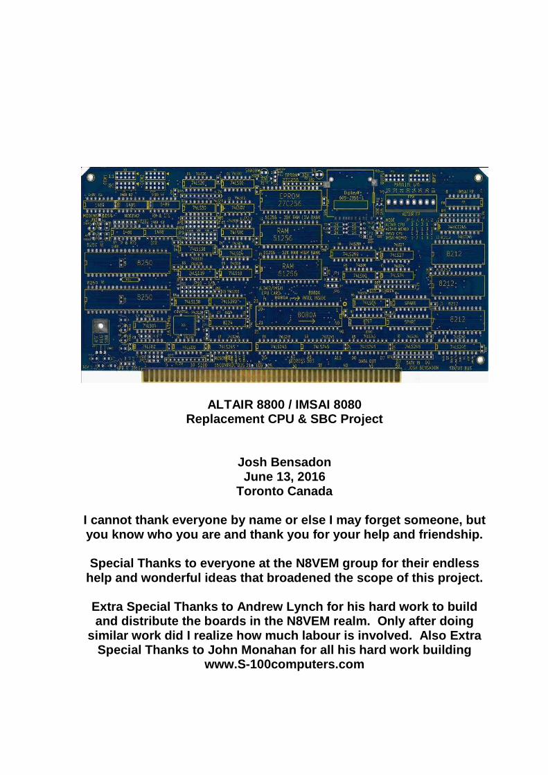
ALTAIR 8800 / IMSAI 8080 Replacement CPU & SBC Project
Josh Bensadon June 13, 2016
Toronto Canada
I cannot thank everyone by name or else I may forge t someone, but you know who you are and thank you for your help an d friendship.
Special Thanks to everyone at the N8VEM group for t heir endless
help and wonderful ideas that broadened the scope o f this project.
Extra Special Thanks to Andrew Lynch for his hard w ork to build and distribute the boards in the N8VEM realm. Only after doing
similar work did I realize how much labour is invol ved. Also Extra Special Thanks to John Monahan for all his hard wor k building
www.S-100computers.com
ALTAIR – IMSAI replacement CPU project.
2
Introduction Thank you for your interest and I am pleased to present revision 1 of this
project. As an electronics hobbyist, I enjoy the roots of my interest as formed by endless hours of studying Popular Electronics and Radio Electronics magazines from the 70’s and 80’s. This drove my interests to the history of personal computers. As such, I would like to include a short history of this project board.
Table of Contents Introduction .......................................................................................................2
Table of Contents ...............................................................................................2
Short History......................................................................................................3
Features .............................................................................................................4 8080A CPU ............................................................................................................. 4 Front Panel Connectors .......................................................................................... 4 Memory ................................................................................................................... 4 I/O ........................................................................................................................... 5
Block Diagram...................................................................................................6
Operation Modes................................................................................................7
Jumper Configuration .......................................................................................7 Board Mode Jumpers - Illustrated ........................................................................... 8 SD Card Diagnostic Jumper – JP3.......................................................................... 8 Shadow ROM Kill Jumper – JP5 ............................................................................. 8 RAM / ROM Select Jumper – JP8 / JP9.................................................................. 9 I/O Address Select Jumper – JP10 ....................................................................... 10
Shadow ROM...................................................................................................11
Memory or I/O only mode................................................................................11 Bus Steering.......................................................................................................... 11
Single Board Computer ...................................................................................12
USB FTDI 232 interface..................................................................................13
Firmware..........................................................................................................14
Modifications Required – Engineering Change Orders ..................................16
Board Assembly ...............................................................................................16
BOM – Bill ofMaterials ...................................................................................19
Final Product ...................................................................................................21
ALTAIR – IMSAI replacement CPU project.
3
Short History
In October 2012, I visited the PC Museum of Ontario (www.pcmuseum.ca) and decided to get their IMSAI 8080 computer running. They did not have a disk drive and the installed boards looked mismatched. On the drive home I thought of building an all-in-one CPU board that would work with the least amount of on-site work. By my next visit in April 2013, I had built the first replacement board on one of Andrew Lynch’s S-100 Unbuffered Prototyping boards1. This first board had 64K of SRAM and a PIC chip to provide a simulated Disk Drive, Console I/O and Boot ROM. An 8Meg Flash memory chip was connected to the PIC’s SPI to host 4 possible disks. The PIC’s USART provided the Console I/O. Upon reset, the PIC would “spoon feed” the 8080A. It supplied the 8080A CPU with instructions that would save a boot strap in RAM. Then a jump to that location would release this “spoon feed” mode and allow the 8080A execute this boot strap program. With the help of Rich Cini’s paper on boot strapping CP/M, I was able to write a copy for this system. On site, I only needed to repair the front panel board and then install this all-in-one CPU board to get a working IMSAI system. After this success, I presented the idea of this board to the N8VEM group and many of your ideas were put on paper and I began working on this version of the board. Many of those ideas are listed in the next chapter that covers features, but one idea that is not listed there was the removal of the PIC chip.
In preparation for this project, I needed to learn KiCad software. I also
saw the benefits of Andrew’s Buffered Prototyping board, but I didn’t like losing all that board real-estate and went to work on a buffered prototyping board that would offer more prototyping area. This side project served as an excellent stepping stone and produced a lot of space to create & debug the prototype.
Although this project did take many hours, I would like to note that it
would have taken ten times longer if it was done back in the 70’s or 80’s because of the lack of all the advanced tools and helpful people there are today.
Revision 1 of the board is very much the same as the original, with fixes
for the previous ECO’s and some new minor features.
1 I found out about Andrew’s prototyping boards from Ebay in the summer of 2012 and since then joined the N8VEM group.
ALTAIR – IMSAI replacement CPU project.
4
Features
Every effort was put into making this project as feature rich as possible. I cannot take credit for all the ideas as most came from the N8VEM group.
8080A CPU • Since this board is intended to operate with the front panels of the ALTAIR
8800 and the IMSAI 8080, the original CPU of these computers was chosen. • This CPU is still widely available on Ebay and other sources. • Historically, the 8080 processor was a significant milestone for INTEL©.
Wikipedia states “The architecture of the 8080 strongly influenced Intel's 8086 CPU architecture, which spawned the x86 family of processors.”
• The 8080A hardware resembles Intel’s first 8 bit processor the 8008 but its programming model & instructions was kept intact when Intel released the 8085
• Zilog copied and built on this programming model because the 8080A was a success. • Runs at 2.048Mhz, which is slightly faster than the original CPU’s that ran at
2.000Mhz. This was done to get the correct baud rates from the UART chips. Hopefully, this minor over clocking shouldn’t affect your software. The original crystal value of 18.000Mhz can be used, only the baud rates will incur some error (which isn’t an issue at lower baud rates).
Front Panel Connectors ALTAIR 8800 – 8 pin Molex
• Original 8 pin Molex connector, 0.156” pin spacing • Located a little to the left of the original, making it easier to plug in the
somewhat short wiring harness. IMSAI 8080 – 16 pin dip
• Standard 16 pin dip, machine socket suggested. • Approximately in the same location as the original IMSAI CPU board • Using the same orientation (pin 1 to the right)
Memory • 32K SRAM chips which are cheap and available everywhere. With 2 chips on
the board, the 8080A can have full access to its whole address range of 64K. • A 32K EPROM chip adds the ability for storing Boot strap programs and
possibly some block(s) of permanent memory. • Selection of onboard RAM/ROM is done in blocks of 8K. Unselected blocks will
permit the 8080A CPU to access those memory ranges from other cards on the S-100 BUS.
• All memory can be disabled by not installing any jumpers
ALTAIR – IMSAI replacement CPU project.
5
I/O Addressing
• All of the following I/O devices are mapped to one of eight (8) selectable blocks of thirty two (32) I/O addresses.
• All other I/O addresses permit the 8080A to access I/O from other cards on the S-100 BUS
• All I/O can be disabled by not installing the jumper Serial Ports
• Uses another popular chip in the 82xx family, the 8250. • Two Serial Ports provided, COM1 and COM2 • Baud rate software selectable • RS-232 output drivers and receivers, configured in 3 steps.
1. Minimal RS-232 (RX/TX + RTS/CTS) for both ports using 1 Driver and 1 Receiver chip
2. Full DSR/DTR support on both ports plus Full modem (DCD + RI) on COM1 by adding another Driver and Receiver chip
3. Full modem (DCD + RI) on COM2 by adding the last Receiver chip • Choice of 10 Pin Header for connection to DB-9 or DB-25 connectors
1. IDC connector maps the 10 pin header to DB-9 IDC pins that connect to a 9 wire ribbon cable. IDC = Insulation Displacement Connector.
2. 1:1 connector maps the 10 pin header to commonly found prefabricated DB-9 and DB-25 connectors as used on recent PC’s. Pin 1 on the header goes to Pin 1 on the DB-9 for DCD, Pin 2 to Pin 2 and so on.
SPI – Serial Peripheral Interface • Uses discrete components, no special chips or programmable microcontrollers. • Runs at the CPU clock of approximately 2Mhz • Interfaces through voltage level shifters (5V to 3.3V) to an SD Memory Card • Four lines are used for SPI communication:
o Clock (Driven by the Master) o Master Out Slave In (MOSI) o Master In Slave Out (MISO) o Device Select (Driven by the Master)
SPI – SD Memory Card • Socket for a full size SD Memory card • Recognizes Type 1, 2 and 3 cards • Allows for mass storage system • Firmware uses files on the SD Memory card as disk images to boot and access
CP/M operating system and files. Parallel Ports
• Uses the 8212 chip, which is still available and was originally used on the IMSAI 8080 CPU board. The strobe and interrupt pin functions offer a little more than just a simple 8 bit latch.
• One eight (8) bit Input port with the ability to strobe the data in. • One eight (8) bit Output port with a strobe (interrupt) signal that pulses every
time the port is written to.
ALTAIR – IMSAI replacement CPU project.
6
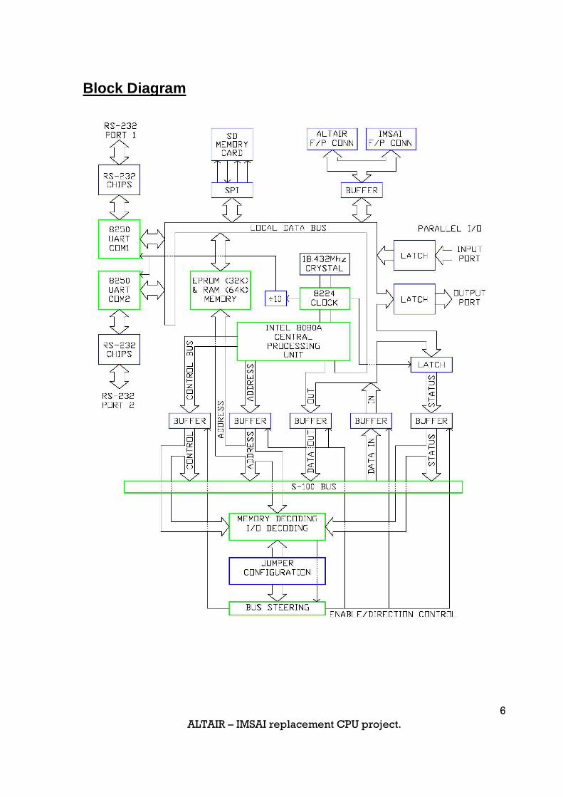
Block Diagram

ALTAIR – IMSAI replacement CPU project.
7
Operation Modes This board has 5 modes of operation. It can serve as:
1. CPU for the ALTAIR 2. Memory and/or I/O card for the ALTAIR 3. CPU for the IMSAI 4. Memory and/or I/O card for the IMSAI 5. Single Board Computer (runs without ALTAIR or IMSAI Front Panel).
This means the card can either be the CPU card, where Data OUT means it’s the originator or as a Memory/I/O card where Data Out means it’s the recipient of the data. This is why all the Memory Address and Control line decoding happens from the S-100 side of the buffers.
Jumper Configuration
ALTAIR – IMSAI replacement CPU project.
8
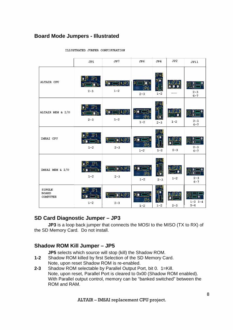
Board Mode Jumpers - Illustrated
SD Card Diagnostic Jumper – JP3 JP3 is a loop back jumper that connects the MOSI to the MISO (TX to RX) of the SD Memory Card. Do not install.
Shadow ROM Kill Jumper – JP5 JP5 selects which source will stop (kill) the Shadow ROM. 1-2 Shadow ROM killed by first Selection of the SD Memory Card.
Note, upon reset Shadow ROM is re-enabled. 2-3 Shadow ROM selectable by Parallel Output Port, bit 0. 1=Kill.
Note, upon reset, Parallel Port is cleared to 0x00 (Shadow ROM enabled). With Parallel output control, memory can be “banked switched” between the ROM and RAM.
ALTAIR – IMSAI replacement CPU project.
9
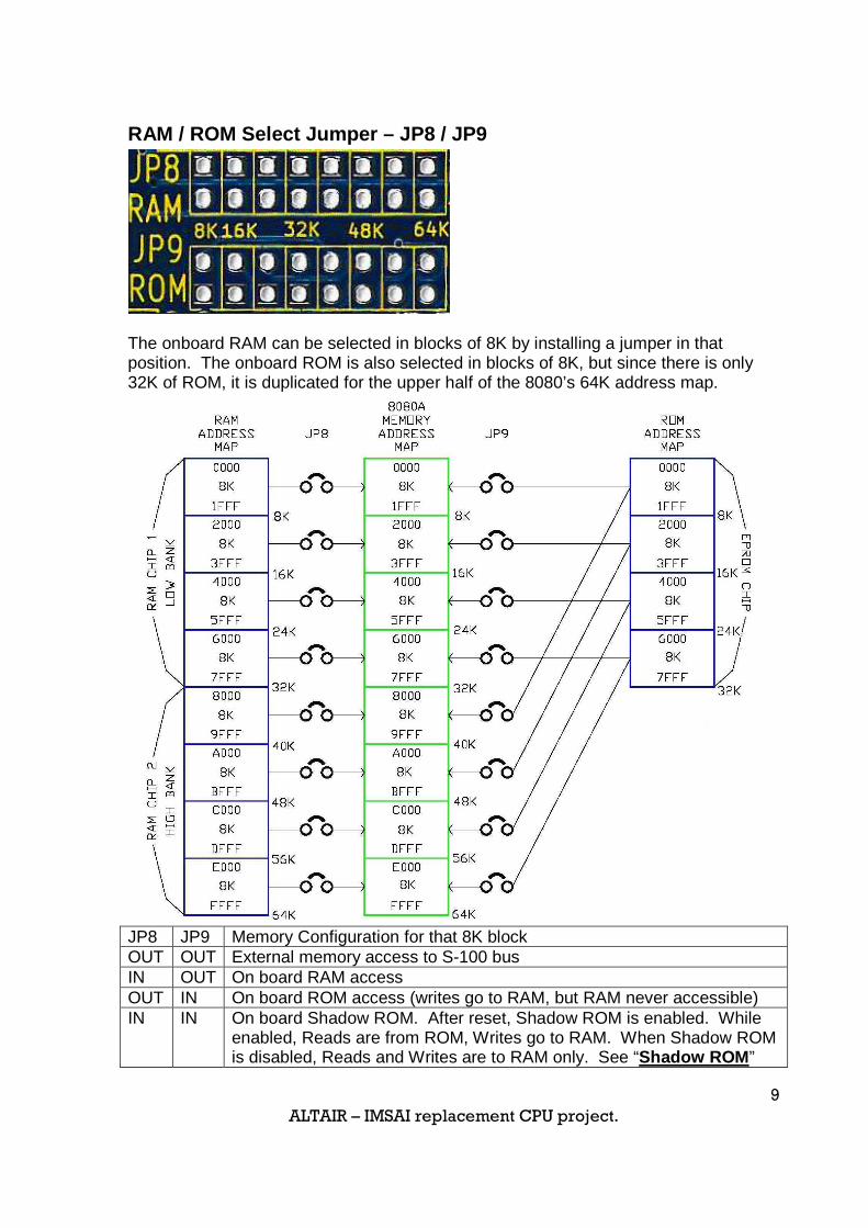
RAM / ROM Select Jumper – JP8 / JP9
The onboard RAM can be selected in blocks of 8K by installing a jumper in that position. The onboard ROM is also selected in blocks of 8K, but since there is only 32K of ROM, it is duplicated for the upper half of the 8080’s 64K address map.
JP8 JP9 Memory Configuration for that 8K block OUT OUT External memory access to S-100 bus IN OUT On board RAM access OUT IN On board ROM access (writes go to RAM, but RAM never accessible) IN IN On board Shadow ROM. After reset, Shadow ROM is enabled. While
enabled, Reads are from ROM, Writes go to RAM. When Shadow ROM is disabled, Reads and Writes are to RAM only. See “Shadow ROM ”

ALTAIR – IMSAI replacement CPU project.
10
I/O Address Select Jumper – JP10
Not marked on the circuit board, but going from left to right the base I/O address for all the onboard I/O is selectable in steps of 32 (0x20). Please install only one (1) jumper to select the base address as given in the table below. I/O addresses not in the selected range will cause I/O from the S-100 bus. If no jumper is installed, then none of the onboard I/O will be selected and all I/O addresses are from the S-100 bus. JP10 I/O addressing None All I/O mapped to S-100 bus Left 0x00 to 0x1F maps to onboard I/O, all other addresses are mapped to S-100 Left+1 0x20 to 0x3F maps to onboard I/O, all other addresses are mapped to S-100 Left+2 0x40 to 0x5F maps to onboard I/O, all other addresses are mapped to S-100 Left+3 0x60 to 0x7F maps to onboard I/O, all other addresses are mapped to S-100 Left+4 0x80 to 0x9F maps to onboard I/O, all other addresses are mapped to S-100 Left+5 0xA0 to 0xBF maps to onboard I/O, all other addresses are mapped to S-100 Left+6 0xC0 to 0xDF maps to onboard I/O, all other addresses are mapped to S-100 Right 0xE0 to 0xFE* maps to onboard I/O, all other addresses are mapped to S-100 Note: When selecting the right most jumper, onboard I/O is not accessed when the front panel switches or LED’s are read/written to at address 0xFF. This range of 32 (0x20) I/O addresses is then divided amongst the onboard I/O devices as follows: Base Address to Base+7 The 8 registers of COM1’s 8250 UART chip. Base+8 to Base+0xF The 8 registers of COM2’s 8250 UART chip. Base+0x10 SPI Shift Register, Writes trigger SPI transfer, Reads only
read the Shift Register containing the received data. Base+0x11 The lsb controls selecting the SD Card. It also can “Kill”
the Shadow ROM based on JP5. 0=Select Card (& Kill). Base+0x18 Reads Only Reads the parallel input port from connector P6 Base+0x18 Writes Only Writes the parallel output port to connector P5 Note: For Base+0x11, only the lsb is latched. The register latching this bit is SET or ON (1) upon a system RESET. This deselects the SD Memory Card and does not affect the Kill Shadow ROM flip/flop. When a “0” is sent to this latch, the SD Memory card is then selected and the Shadow ROM is killed (if configured to do so by JP5). Since it’s a flip/flop controlling the Shadow ROM, there is no way to map the Shadow ROM back without a system reset. There is however the possibility to rewire pin 10 of IC E5. First it must be cut away from Pin 9 of IC E5, then it can be jumpered to some other means of resetting this flip/flop. See the schematics for more details.

ALTAIR – IMSAI replacement CPU project.
11
Shadow ROM By installing both JP8 and JP9 for the same block, it is possible to start out with ROM then convert that 8080 address space to RAM by “killing” the Shadow ROM. The kill to shadow ROM can be done in 2 ways, see Jumper 5 configuration. The advantage of using the Output port, is that the Shadow ROM can be brought back into the 8080 address space, in effect, this would be like bank switching. For example, you might put some floating point math routines in ROM then only switch in those routines when you need them. By far, the most practical use of Shadow ROM is to allow the system to boot up, copy the ROM code to RAM space as needed, then kill the Shadow ROM. The biggest reason for this approach is for using the CP/M system, which is commonly intended for systems with RAM in the lower memory addresses. However, since the 8080A begins program execution at 0000, it would be useful to have ROM there at 0000 (temporarily) to load CP/M (or a bootstrap) then switch that space to RAM to run CP/M. Note, part of loading CP/M will require this space to be RAM already.
Memory or I/O only mode When operating in Memory or I/O only mode, the 8080A cpu does not need to be installed, even if it is installed, it will not run because the Hold line will go high to effectively disable the 8080A’s control over the bus. In this mode, all Memory and I/O address selections will continue to work but only for an external processor on the S-100 bus. This is accomplished by reversing the Data-IN and Data-OUT buffer direction. The schematic shows this as M or S mode, where M is “master” ie CPU mode and S is “slave” ie Memory or I/O only mode.
Bus Steering The Master/Slave jumper (JP4) and the ALTAIR/IMSAI jumper (JP6) with the External Memory jumper (JP2) control the Data-IN and Data-OUT bus direction and enabling.

ALTAIR – IMSAI replacement CPU project.
12
Single Board Computer New on this version is the ability to run as a Single Board Computer. The ALTAIR and IMSAI computers use a front panel. This panel, aside from the memory examine and deposit functions, controls the computer with Run/Stop and Reset. It also provides the Memory Write signal. Without the front panel, the Run will float high, but the board has no Power On Reset, so a momentary short on the RESET input is required. Jumper block JP11 will rewire an NOR gate to provide the needed Memory Write. If you are installing JP11, two traces must be cut under this jumper block.
A third hole is provided on the bottom right of the board. The card handles can be omitted and 4 stand offs can be used on the board (the 4th hole is shared with the voltage regulator screw). Alternate Power source. Near JP11, a new connector is provided to access the +8V, +16V and -16V directly. This connector is labeled +5V, -12V, +12V. Voltage Regulators A3, A4, A7 and B7 can be omitted and jumper as shown to have their output pin connected with a wire to their input pin. You can also install the regulators and jumper the pins from the bottom of the board. Caution , do not plug such a board into an S-100 slot, the 8V will kill the chips . Please put tape or a label on the S-100 fingers to indicate a 5V board. A PC power supply can now be rewired to provide this power.

ALTAIR – IMSAI replacement CPU project.
13
Be sure to wrap the label or tape to both sides, so power fingers can never be accidentally connected to an 8V S-100 slot.
USB FTDI 232 interface A new connector is provided right above chip B3. This can be used to install an FT232 type USB serial interface. Remove JP12 to isolate the DTR signal and carefully pull out pin 6 of IC C2 to isolate the RX signal (the jumper for this was missed).
Pinout for the module: Pin 1 -DTR Pin 2 -RX Pin 3 -TX Pin 4 - Pin 5 - Pin 6 -GND
ALTAIR – IMSAI replacement CPU project.
14
Firmware As of May 31, 2016, There are two forms of the firmware. The original firmware was revised to version 1.2. This version is described below. The next release had a major update, so it began at version 2.0 and is currently at version 2.4 for the ROM chip. The major update was to minimize the firmware in ROM and allow the loading of the firmware from the SD card. There are two parts to the firmware now. Part 1- Boot Loader . This is at version 2.4 and only initializes the SD card and offers a minimized menu as follows: ALTAIR/IMSAI 8080 CPU BOARD BOOT LOADER – Josh Bens adon (Feb 22, 2015) <D> -Directory <R> -RAM Test <V> -View Load > ….. Five dots will slowly count away your time to enter an option, at the end of that time the boot loader will attempt to load a file named “BIOS.HEX” from the SD card and execute it. You may select D to list a directory of the FAT16 files on the SD card, then enter the name of any hex file you wish to load. The R command does a RAM test on the upper 4K of RAM. This section of RAM is used by the system and can’t be tested (without crashing) the Monitor program located in the BIOS.HEX file. The V command sets a flag that will cause the load to be viewed. Note, when loading a HEX file, the HEX file includes the address of where the data is to be loaded. The hex file can be loaded anywhere in memory, including the lower 8K which is where the Shadow ROM is presently executing the Boot Loader. All writes go to RAM and at the end of the load, the ROM is swapped out and execution is passed to the first byte loaded from the HEX file. You can have subroutines or Data before your code, but the hex file must be arranged so that the first byte loaded is your program start. Eg: Addr Bytes 1000 xx xx xx <Program starts at 0x1000 0000 dd dd dd <data in page 0 0100 ss ss ss <subroutines in page 1 You can also simply edit your hex file to make it so. This arrangement of a boot loader now allows you to load and run any hex file you want, not just the part 2 of the firmware.
ALTAIR – IMSAI replacement CPU project.
15
Part 2 – Monitor & CP/M Loader. In the file BIOS.HEX, you may either run the Monitor or setup the virtual disks and Boot CP/M. The screen appears as follows: ALTAIR/IMSAI 8080 CPU BOARD – Josh Bensadon v2.3 (J an 2015) Init SD Type#_ ACMD41+MBR S Type__ PBR S VOL=….. SY S=FAT16 M – Monitor C – Boot CP/M 1 – Disk A = DISK-A.BIN –EXISTS 2 – Disk B = DISK-B.BIN -EXISTS 3 – Disk C = DISK-C.BIN -EXISTS 4 – Disk D = DISK-D.BIN -EXISTS Option M enters you into the Monitor Mode. You can return to the BIOS menu by entering G DB00 (Go execute at 0xDB00), or if you previously had CP/M loaded, you can return to CP/M with G 0. Option C will boot CP/M with disks A to D assigned to the displayed file names. Pressing 1 to 4 will allow you to enter a different FAT16 file to work as the virtual disk for that drive. The file is tested to see if it exists and if its size is correct. It expects exactly 256,256 bytes which is the number of bytes that can be stored on a single density disk of 77 Tracks with 26 Sectors of 128 bytes each. These virtual disk files are nothing more than straight sector for sector copies of what would be a real disk. That is to say, the first 128 bytes of the file hold Track 0, Sector 0 data, the next 128 bytes hold Track 0, Sector 1. This pattern repeats for all sectors on that track then carries on for the next Track. Version 1.2 – Old version. Included in the zip file are the source code and all the tools necessary to assemble it. There are 2 parts, the first is a 48 byte boot loader that will relocate the next part into RAM at the high addresses. The next part holds a monitor and the BIOS for CP/M. The two parts are concatenated by the 2nd batch file to produce the EPROM image. Also included, is a file that is 256,256 bytes long, which is the size of an IBM 3740 formated disk (77 tracks of 26 sectors of 128 bytes each). This file has CP/M 2.2 on it and the firmware can load it and run CP/M. There is an issue with selecting another drive, but that will be debugged in the future. To run this firmware, you must jumper at least the first 8K block of RAM and the two top blocks of 8K RAM. Unless you have external RAM, you will need to install all the RAM jumpers. The first 8K block of ROM should also be jumpered, this will allow the ROM to be in control until after it copies and turns off the SHADOW ROM feature.

ALTAIR – IMSAI replacement CPU project.
16
Modifications Required – Engineering Change Orders This Version of the board does not require any ECO’s. Jumper JP11 is already connected by traces on the board for ALTAIR or IMSAI. If you intend to use the board as a Single Board Computer, you will need to cut these traces.
Board Assembly It’s always easier to install the components that have the lowest profile first. Here’s an approximate list in that order.
1. Cut Trace under JP11 if you plan to use as Single Board Computer. 2. SD Memory Card Socket, Digikey # 609-3956-1 3. Discrete resistors and diode. 4. Ceramic capacitors and resistor networks. 5. IC’s and/or IC Sockets. Sockets are suggested for the LSI and RS-232 chips
but it’s your choice. A machine socket work best for the IMSAI FP connector. 6. All Voltage Regulators. The 7805C needs a decent heat sink. 7. All Jumper Blocks (cut traces if installing JP11) 8. Polarized capacitors 9. The ALTAIR FP connector. 10. Crystal. It may not be the highest profile, but it’s a delicate component, so it’s
recommended to go in last. Note: The 8080A chip is reversed to all the other chips (pin 1 to the right). Prior to powering up the board, it’s always advisable to look for solder shorts and ohm out the VCC and GND lines across any IC to ensure there isn’t a power supply short. Also, ohm out all the other voltage regulator outputs to ground to prevent excessive current and damage in case of shorts. Ohm readings to GND should be anything higher than 100 ohms, it varies depending on your meter since these are semiconductors. Power up the board without any IC’s, measure the voltages to the 8080A socket. You should only get +12V on pin 28 and -5V on pin 11. You will also get +5V on pin 20 and the data lines (pins 3 to 10). If you get the +12 or -5 on any other pin, look for solder shorts and/or micro shorts on the board to correct the problem. This will save you from destroying the 8080A CPU. John Monahan wrote a very comprehensive guide to building this board: http://s100computers.com/My%20System%20Pages/8080%20CPU%20Board/8080%20CPU%20Board.htm

ALTAIR – IMSAI replacement CPU project.
17
The Voltage Regulator. This board uses just over 1Amp, so it is very important that a 7805C be used which can provide 1.5Amp. When using this regulator, a heat sink is required. Shown here is a 1.5W @ 40 degrees heat sink (Digikey HS107-ND). While it gets hot to the touch it does work, provided the input voltage does not go above 8V. An alternative to the linear voltage regulator is a very cool (literally) switching DC-DC converter made by Murata Power Solutions Inc. PN: OKI-78SR-5/1.5-W36-C (Digikey 811-2196-5-ND). However, this DC-DC converter needs a little modification. It is a vertical mount. Although they do sell a Horizontal mount version, it is not pin compatible with the 7805.

ALTAIR – IMSAI replacement CPU project.
18
The modification is simple. The DC-DC converter looks like this.
Step 1. Bend pins up. Carefully bend them while applying counter torque to prevent the pin from kinking. You want that pin straight.
Step 2. Hold in vise, heat pins and push them down / through the module.
Final Result looks like this. Repeat for all pins
ALTAIR – IMSAI replacement CPU project.
19
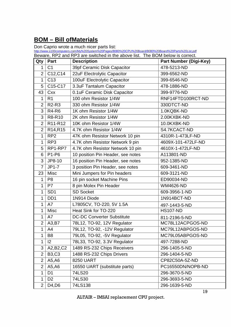
BOM – Bill ofMaterials Don Caprio wrote a much nicer parts list: http://www.s100computers.com/My%20System%20Pages/8080%20CPU%20Board/8080%20Board%20Parts%20List.pdf Beware, RP2 and RP3 are switched in the above list. The BOM below is correct. Qty Part Description Part Number (Digi-Key)
1 C1 39pf Ceramic Disk Capacitor 478-5213-ND 2 C12,C14 22uF Electrolytic Capacitor 399-6562-ND 1 C13 100uF Electrolytic Capacitor 399-6546-ND 5 C15-C17 3.3uF Tantalum Capacitor 478-1886-ND
43 Cxx 0.1uF Ceramic Disk Capacitor 399-9776-ND 1 R1 100 ohm Resistor 1/4W RNF14FTD100RCT-ND 2 R2-R3 330 ohm Resistor 1/4W 330DTCT-ND 3 R4-R6 1K ohm Resistor 1/4W 1.0KQBK-ND 3 R8-R10 2K ohm Resistor 1/4W 2.00KXBK-ND 2 R11-R12 10K ohm Resistor 1/4W 10.0KXBK-ND 2 R14,R15 4.7K ohm Resistor 1/4W S4.7KCACT-ND 1 RP2 47K ohm Resistor Network 10 pin 4310R-1-473LF-ND 1 RP3 4.7K ohm Resistor Network 9 pin 4609X-101-472LF-ND 5 RP1-RP7 4.7K ohm Resistor Network 10 pin 4610X-1-472LF-ND 6 P1-P6 10 position Pin Header, see notes A113801-ND 3 JP8-10 16 position Pin Header, see notes 952-1385-ND 7 JP1-7 3 position Pin Header, see notes 609-3461-ND
23 Misc Mini Jumpers for Pin headers 609-3121-ND 1 P8 16 pin socket Machine Pins ED90034-ND 1 P7 8 pin Molex Pin Header WM4626-ND 1 SD1 SD Socket 609-3956-1-ND 1 DD1 1N914 Diode 1N914BCT-ND 1 A7 L7805CV, TO-220, 5V 1.5A 497-1443-5-ND 1 Misc Heat Sink for TO-220 HS107-ND 1 A7 DC-DC Converter Substitute 811-2196-5-ND 2 A3,B7 78L12, TO-92, 12V Regulator MC78L12ACPGOS-ND 1 A4 79L12, TO-92, -12V Regulator MC79L12ABPGOS-ND 1 B8 79L05, TO-92, -5V Regulator MC79L05ABPGOS-ND 1 I2 78L33, TO-92, 3.3V Regulator 497-7288-ND 3 A2,B2,C2 1489 RS-232 Chips Receivers 296-1405-5-ND 2 B3,C3 1488 RS-232 Chips Drivers 296-1404-5-ND 2 A5,A6 8250 UART CP82C50A-5Z-ND 2 A5,A6 16550 UART (substitute parts) PC16550DN/NOPB-ND 1 D1 74LS20 296-3670-5-ND 1 D2 74LS30 296-3693-5-ND 2 D4,D6 74LS138 296-1639-5-ND

ALTAIR – IMSAI replacement CPU project.
20
1 D5 74LS139 296-1640-5-ND 3 C7,E4,H5 74LS04 296-1629-5-ND 2 C8,E2 74LS02 296-1627-5-ND 4 D8,E1,H5, 74LS00 296-1626-5-ND 1 E6 74LS390 296-26516-5-ND 1 E5 74LS10 296-1634-5-ND 6 E8-J8 74LS245 296-1655-5-ND 1 F1 27C256 32K EPROM AT27C256R-70PU-ND 2 F3,F5 51256 32K Static RAM 1450-1033-ND 3 J3,J5,J7 8212, 8-bit I/O Port 1 E7 8224 Clock Generator 1 F7 Intel 8080A CPU 1 H4 74LS299 296-3692-5-ND 1 I4 74LS27 296-14890-5-ND 1 I5 74LS74 296-1668-5-ND 1 H7 8T97 or 74LS367 296-3701-5-ND 1 J2 74HCT245 296-1612-5-ND 1 X1 18.432Mhz Crystal ECS-184-20-1X X1036-ND
19 14 Pin IC Sockets ED3045-5-ND 6 16 Pin IC Sockets 1175-1477-ND 8 20 Pin IC Sockets 1175-1479-ND 3 24 Pin IC Sockets, 0.6” ED90118-ND 3 28 Pin IC Sockets, 0.6” 1175-1480-ND 3 40 Pin IC Sockets, 0.6” 1175-1481-ND 2 9 Pin DB connector, IDC S9597-ND 2 10 Pin Header, IDC MSC10A-ND 2 Ribbon Cable 10c x 24" 2 Card Handles Bivar CP-06 WE 492-1024-ND 1 SD Card (1GB or less)
Notes:
• Resistors can be 1/8 to 1/4 watt, the 1/4 watt are easier to handle but 1/8 watt are smaller, it’s your choice.
• Only 4 pin headers are needed between P1 to P6, only one header for either 1:1 or IDC needs to be installed. No harm to install both, in which case you will need 6 of these headers.
• Recommend buying some long pin headers and just cutting to lengths needed. • Optional to add IC sockets where desired, Recommended for all the LSI chips
and RS232 chips.
ALTAIR – IMSAI replacement CPU project.
21
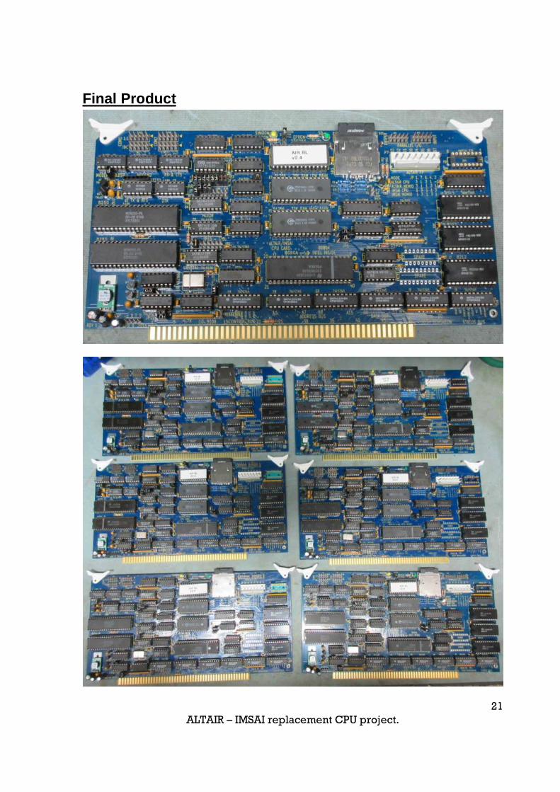
Final Product