Embed Size (px)
Citation preview
Altera Confidential Page 1
Altera JESD204B Analog Loopback Demo Reference Design User Guide
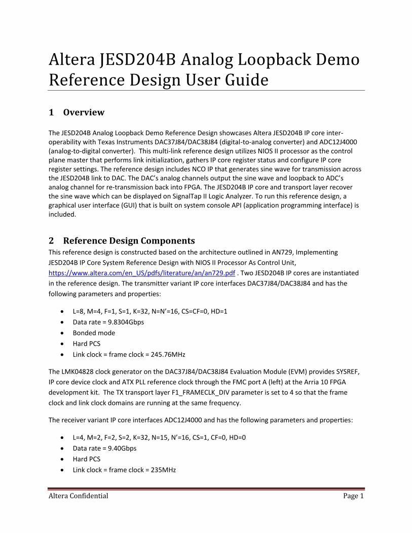
1 Overview The JESD204B Analog Loopback Demo Reference Design showcases Altera JESD204B IP core inter-operability with Texas Instruments DAC37J84/DAC38J84 (digital-to-analog converter) and ADC12J4000 (analog-to-digital converter). This multi-link reference design utilizes NIOS II processor as the control plane master that performs link initialization, gathers IP core register status and configure IP core register settings. The reference design includes NCO IP that generates sine wave for transmission across the JESD204B link to DAC. The DAC’s analog channels output the sine wave and loopback to ADC’s analog channel for re-transmission back into FPGA. The JESD204B IP core and transport layer recover the sine wave which can be displayed on SignalTap II Logic Analyzer. To run this reference design, a graphical user interface (GUI) that is built on system console API (application programming interface) is included.
2 Reference Design Components This reference design is constructed based on the architecture outlined in AN729, Implementing
JESD204B IP Core System Reference Design with NIOS II Processor As Control Unit,
https://www.altera.com/en_US/pdfs/literature/an/an729.pdf . Two JESD204B IP cores are instantiated
in the reference design. The transmitter variant IP core interfaces DAC37J84/DAC38J84 and has the
following parameters and properties:
L=8, M=4, F=1, S=1, K=32, N=N’=16, CS=CF=0, HD=1
Data rate = 9.8304Gbps
Bonded mode
Hard PCS
Link clock = frame clock = 245.76MHz
The LMK04828 clock generator on the DAC37J84/DAC38J84 Evaluation Module (EVM) provides SYSREF,
IP core device clock and ATX PLL reference clock through the FMC port A (left) at the Arria 10 FPGA
development kit. The TX transport layer F1_FRAMECLK_DIV parameter is set to 4 so that the frame
clock and link clock domains are running at the same frequency.
The receiver variant IP core interfaces ADC12J4000 and has the following parameters and properties:
L=4, M=2, F=2, S=2, K=32, N=15, N’=16, CS=1, CF=0, HD=0
Data rate = 9.40Gbps
Hard PCS
Link clock = frame clock = 235MHz
Altera Confidential Page 2
The LMK04828 clock generator on the ADC12J4000 EVM provides SYSREF, IP core device clock and CDR
reference clock through the FMC port B (right) at the Arria 10 FPGA development kit. RX transport layer
F2_FRAMECLK_DIV parameter is set to 2 so that the frame clock and link clock domains are running at
the same frequency.
The NIOS II processor is the AV-MM master that controls and gathers information from the IP core CSR
interfaces. The AV-MM bus runs on 100MHz management clock. This clock is asynchronous to link and
frame clock domains. The SPI interface is not used in this demo because the converters and clock
generators on the EVM are configured through the converters EVM GUI software. The AV-ST buses are
exposed at the top level for integration with user logic. These AV-ST buses operate in frame clock
domain of the respective JESD204B link.
Figure 1: Simplified Block Diagram
The JESD204B IP cores, transport layers, pattern generator/checker, core PLL and ATX PLL are
instantiated in QSYS. There are 6 pattern generator modes and 3 pattern checker modes available:
PRBS
Ramp
Alternate checker board
Low frequency sine wave (in pattern generator only)
High frequency sine wave (in pattern generator only)
User test pattern (in pattern generator only)
Altera Confidential Page 3
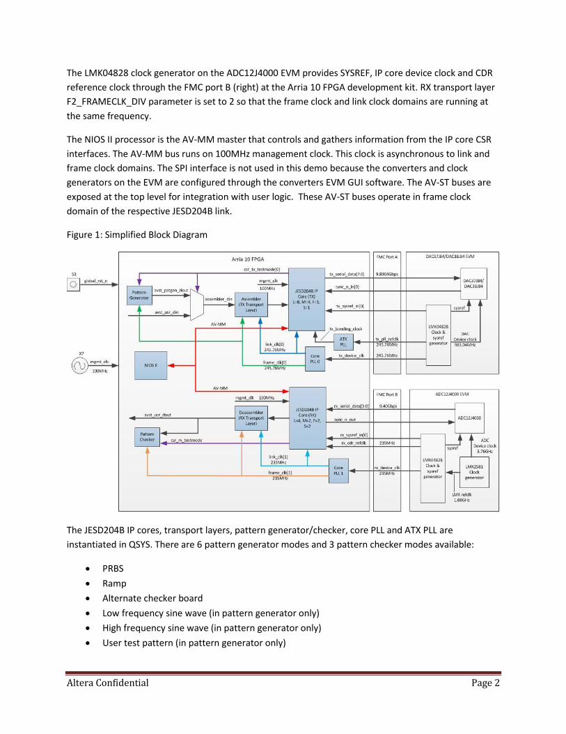
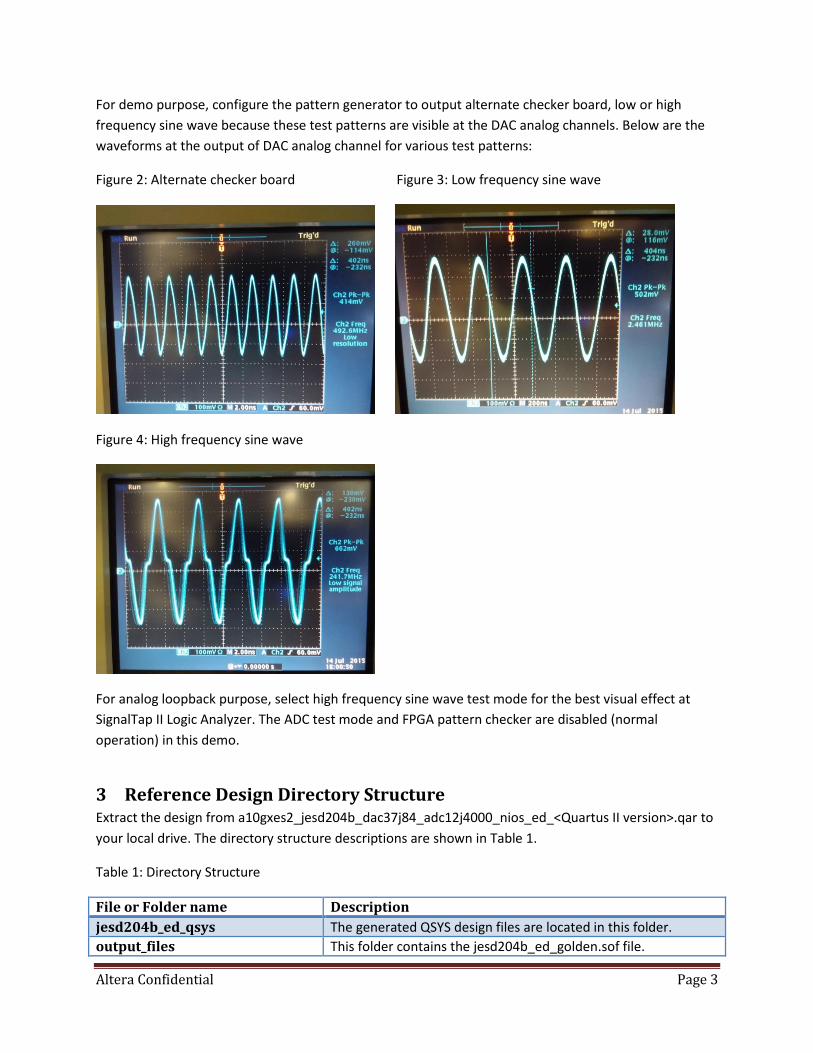
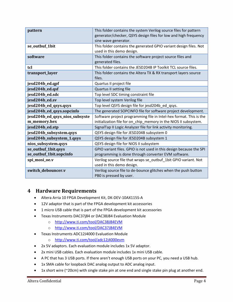
For demo purpose, configure the pattern generator to output alternate checker board, low or high
frequency sine wave because these test patterns are visible at the DAC analog channels. Below are the
waveforms at the output of DAC analog channel for various test patterns:
Figure 2: Alternate checker board Figure 3: Low frequency sine wave
Figure 4: High frequency sine wave
For analog loopback purpose, select high frequency sine wave test mode for the best visual effect at
SignalTap II Logic Analyzer. The ADC test mode and FPGA pattern checker are disabled (normal
operation) in this demo.
3 Reference Design Directory Structure Extract the design from a10gxes2_jesd204b_dac37j84_adc12j4000_nios_ed_<Quartus II version>.qar to
your local drive. The directory structure descriptions are shown in Table 1.
Table 1: Directory Structure
File or Folder name Description
jesd204b_ed_qsys The generated QSYS design files are located in this folder.
output_files This folder contains the jesd204b_ed_golden.sof file.
Altera Confidential Page 4
pattern This folder contains the system Verilog source files for pattern generator/checker, QSYS design files for low and high frequency sine wave generator.
se_outbuf_1bit This folder contains the generated GPIO variant design files. Not used in this demo design.
software This folder contains the software project source files and generated files.
tcl This folder contains the JESD204B IP Toolkit TCL source files.
transport_layer This folder contains the Altera TX & RX transport layers source files.
jesd204b_ed.qpf Quartus II project file
jesd204b_ed.qsf Quartus II setting file
jesd204b_ed.sdc Top level SDC timing constraint file
jesd204b_ed.sv Top level system Verilog file
jesd204b_ed_qsys.qsys Top level QSYS design file for jesd204b_ed_qsys.
jesd204b_ed_qsys.sopcinfo The generated SOPCINFO file for software project development.
jesd204b_ed_qsys_nios_subsystem_memory.hex
Software project programming file in Intel-hex format. This is the initialization file for on_chip_memory in the NIOS II subsystem.
jesd204b_ed.stp SignalTap II Logic Analyzer file for link activity monitoring.
jesd204b_subsystem.qsys QSYS design file for JESD204B subsystem 0
jesd204b_subsystem_1.qsys QSYS design file for JESD204B subsystem 1
nios_subsystem.qsys QSYS design file for NIOS II subsystem
se_outbuf_1bit.qsys se_outbuf_1bit.sopcinfo
GPIO variant files. GPIO is not used in this design because the SPI programming is done through converter EVM software.
spi_mosi_oe.v Verilog source file that wraps se_outbuf_1bit GPIO variant. Not used in this demo design.
switch_debouncer.v Verilog source file to de-bounce glitches when the push button PB0 is pressed by user.
4 Hardware Requirements Altera Arria 10 FPGA Development Kit, DK-DEV-10AX115S-A
12V adaptor that is part of the FPGA development kit accessories
1 micro USB cable that is part of the FPGA development kit accessories
Texas Instruments DAC37j84 or DAC38J84 Evaluation Module
o http://www.ti.com/tool/DAC38J84EVM
o http://www.ti.com/tool/DAC37J84EVM
Texas Instruments ADC12J4000 Evaluation Module
o http://www.ti.com/tool/adc12j4000evm
2x 5V adaptors. Each evaluation module includes 1x 5V adaptor.
2x mini USB cables. Each evaluation module includes 1x mini USB cable.
A PC that has 3 USB ports. If there aren’t enough USB ports on your PC, you need a USB hub.
1x SMA cable for loopback DAC analog output to ADC analog input.
1x short wire (~20cm) with single stake pin at one end and single stake pin plug at another end.
Altera Confidential Page 5
500MHz – 1GHz low bandwidth oscilloscope (optional)
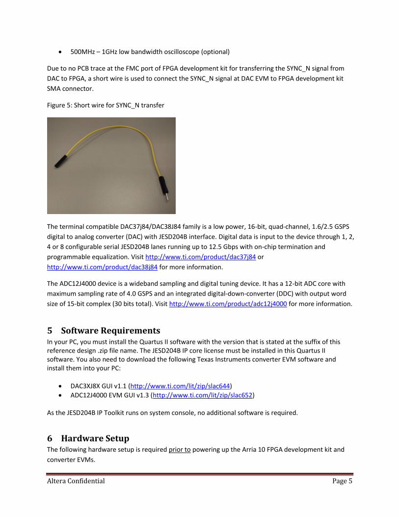
Due to no PCB trace at the FMC port of FPGA development kit for transferring the SYNC_N signal from
DAC to FPGA, a short wire is used to connect the SYNC_N signal at DAC EVM to FPGA development kit
SMA connector.
Figure 5: Short wire for SYNC_N transfer
The terminal compatible DAC37j84/DAC38J84 family is a low power, 16-bit, quad-channel, 1.6/2.5 GSPS
digital to analog converter (DAC) with JESD204B interface. Digital data is input to the device through 1, 2,
4 or 8 configurable serial JESD204B lanes running up to 12.5 Gbps with on-chip termination and
programmable equalization. Visit http://www.ti.com/product/dac37j84 or
http://www.ti.com/product/dac38j84 for more information.
The ADC12J4000 device is a wideband sampling and digital tuning device. It has a 12-bit ADC core with
maximum sampling rate of 4.0 GSPS and an integrated digital-down-converter (DDC) with output word
size of 15-bit complex (30 bits total). Visit http://www.ti.com/product/adc12j4000 for more information.
5 Software Requirements In your PC, you must install the Quartus II software with the version that is stated at the suffix of this reference design .zip file name. The JESD204B IP core license must be installed in this Quartus II software. You also need to download the following Texas Instruments converter EVM software and install them into your PC:
DAC3XJ8X GUI v1.1 (http://www.ti.com/lit/zip/slac644)
ADC12J4000 EVM GUI v1.3 (http://www.ti.com/lit/zip/slac652) As the JESD204B IP Toolkit runs on system console, no additional software is required.
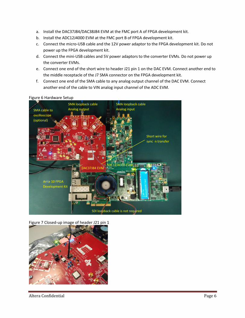
6 Hardware Setup The following hardware setup is required prior to powering up the Arria 10 FPGA development kit and
converter EVMs.
Altera Confidential Page 6
a. Install the DAC37J84/DAC38J84 EVM at the FMC port A of FPGA development kit.
b. Install the ADC12J4000 EVM at the FMC port B of FPGA development kit.
c. Connect the micro-USB cable and the 12V power adaptor to the FPGA development kit. Do not
power up the FPGA development kit.
d. Connect the mini-USB cables and 5V power adaptors to the converter EVMs. Do not power up
the converter EVMs.
e. Connect one end of the short wire to header J21 pin 1 on the DAC EVM. Connect another end to
the middle receptacle of the J7 SMA connector on the FPGA development kit.
f. Connect one end of the SMA cable to any analog output channel of the DAC EVM. Connect
another end of the cable to VIN analog input channel of the ADC EVM.
Figure 6 Hardware Setup
Figure 7 Closed-up image of header J21 pin 1
SDI loopback cable is not required
SMA loopback cable
Analog output SMA cable to
oscilloscope
(optional)
SMA loopback cable
Analog input
DAC37J84 EVM ADC12J4000 EVM
Short wire for
sync_n transfer
Arria 10 FPGA
Development Kit
Altera Confidential Page 7
7 Software Setup The converters need to be configured appropriately in order to interoperate with FPGA. A set of SPI
programming configuration files are available with the installation of the converter EVM software. Some
customizations to the converter settings as defined in the configuration files are needed to suit the
JESD204B IP core parameters settings of this reference design. The following steps are preparation prior
to running the reference design.
7.1 DAC3XJ8X GUI Extract the 841_iot_9g_2clk.cfg file from a10gxes2_jesd204b_dac37j84_adc12j4000_nios_ed_<Quartus
II version>.zip and save it into your local drive. This file will be used when configuring the DAC.
7.2 ADC12J4000EVM GUI Backup the ADC12J4000_DB4_DDR_P54.cfg and LMK04828_DB4_DDR_P54_Fs_3500Msps.cfg files in
“<EVM software installation path>\Texas Instruments\ADC12J4000EVM GUI\Configuration Files” and
“<EVM software installation path>\Texas Instruments\ADC12J4000EVM GUI v1.1\Configuration Files”
folders. Extract the ADC12J4000_DB4_DDR_P54.cfg and LMK04828_DB4_DDR_P54_Fs_3500Msps.cfg
files from a10gxes2_jesd204b_dac37j84_adc12j4000_nios_ed_<Quartus II version>.zip and put these 2
files into the above folders.
The DAC and ADC EVM GUI require the USB drivers to be installed on your PC. Your PC should be
connected to Internet. Power up both EVMs. The EVMs are powered by the 5V adaptors; the ADC EVM
has a switch to turn on/off the power. The FPGA development kit can remain unpowered. The USB
driver installation should begin automatically. Below image shows the successful installation of the USB
drivers.
Figure 8: DAC3XJ8X and ADC12J4000EVM GUI USB Devices in Windows Device Manager
8 Running the Reference Design After the hardware is setup and the required EVM software is installed, you can run this reference with
the following steps. The procedure begins with programming the converters and clock generator.
Because all transceiver reference clocks and the CLKUSR clock must be free running and stable at the
start of FPGA configuration to successfully complete the calibration process for optimal transceiver
performance, the clock generators at the EVMs must be programmed before FPGA is configured. After
the design is loaded into FPGA, the JESD204B IP Toolkit is launched. The IP Toolkit allows you to program
the IP core settings and observe the link status. Lastly, the sine wave can be observed at the SignalTap II
Altera Confidential Page 8
Logic Analyzer. Optionally, you can view the waveform from the analog output of the DAC at a low
bandwidth oscilloscope.
8.1 Program Converters and Clock Generators on EVMs a. Power up the DAC EVM, ADC EVM and FPGA development kit. There is no specific power up
sequence for these 3 boards.
b. Make sure the EVMs and FPGA development kits USB interfaces enumerate successfully and the
boards are ready for operation. You can check the status in Windows Device Manager.
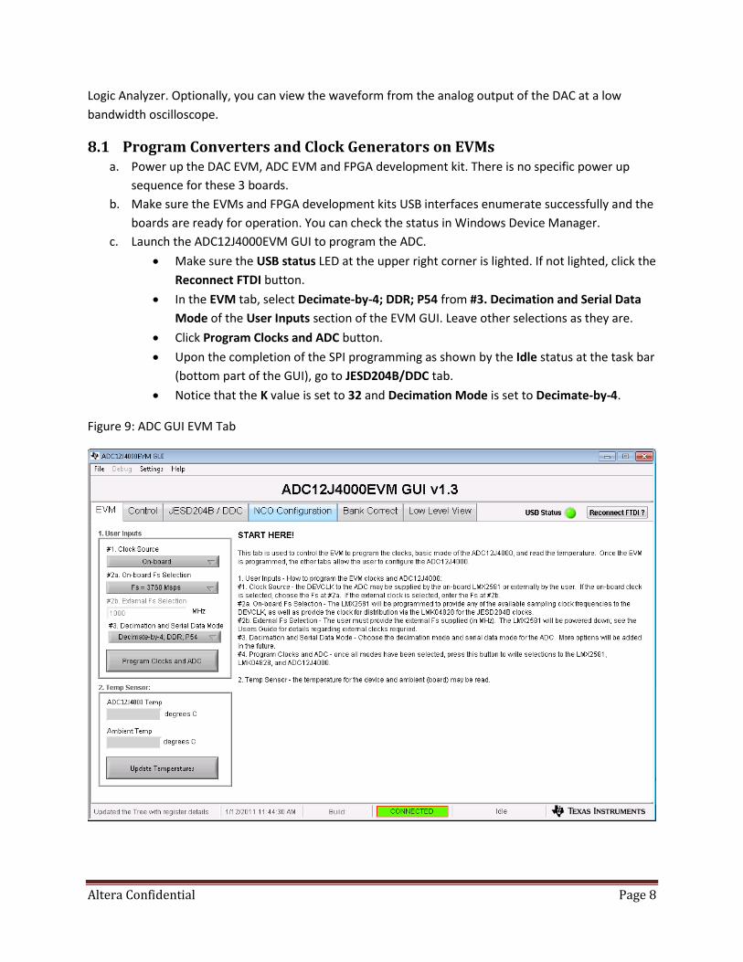
c. Launch the ADC12J4000EVM GUI to program the ADC.
Make sure the USB status LED at the upper right corner is lighted. If not lighted, click the
Reconnect FTDI button.
In the EVM tab, select Decimate-by-4; DDR; P54 from #3. Decimation and Serial Data
Mode of the User Inputs section of the EVM GUI. Leave other selections as they are.
Click Program Clocks and ADC button.
Upon the completion of the SPI programming as shown by the Idle status at the task bar
(bottom part of the GUI), go to JESD204B/DDC tab.
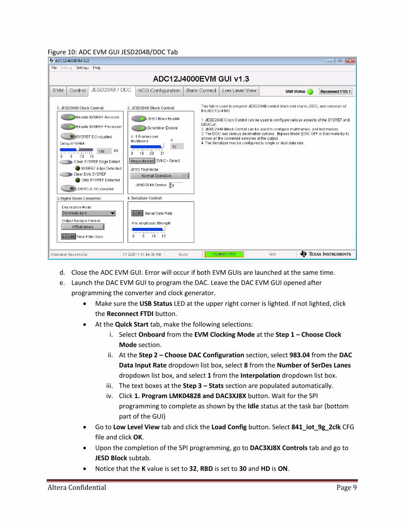
Notice that the K value is set to 32 and Decimation Mode is set to Decimate-by-4.
Figure 9: ADC GUI EVM Tab
Altera Confidential Page 9
Figure 10: ADC EVM GUI JESD204B/DDC Tab
d. Close the ADC EVM GUI. Error will occur if both EVM GUIs are launched at the same time.
e. Launch the DAC EVM GUI to program the DAC. Leave the DAC EVM GUI opened after
programming the converter and clock generator.
Make sure the USB Status LED at the upper right corner is lighted. If not lighted, click
the Reconnect FTDI button.
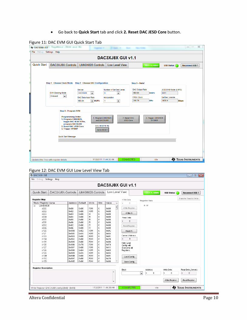
At the Quick Start tab, make the following selections:
i. Select Onboard from the EVM Clocking Mode at the Step 1 – Choose Clock
Mode section.
ii. At the Step 2 – Choose DAC Configuration section, select 983.04 from the DAC
Data Input Rate dropdown list box, select 8 from the Number of SerDes Lanes
dropdown list box, and select 1 from the Interpolation dropdown list box.
iii. The text boxes at the Step 3 – Stats section are populated automatically.
iv. Click 1. Program LMK04828 and DAC3XJ8X button. Wait for the SPI
programming to complete as shown by the Idle status at the task bar (bottom
part of the GUI)
Go to Low Level View tab and click the Load Config button. Select 841_iot_9g_2clk CFG
file and click OK.
Upon the completion of the SPI programming, go to DAC3XJ8X Controls tab and go to
JESD Block subtab.
Notice that the K value is set to 32, RBD is set to 30 and HD is ON.
Altera Confidential Page 10
Go back to Quick Start tab and click 2. Reset DAC JESD Core button.
Figure 11: DAC EVM GUI Quick Start Tab
Figure 12: DAC EVM GUI Low Level View Tab
Altera Confidential Page 11
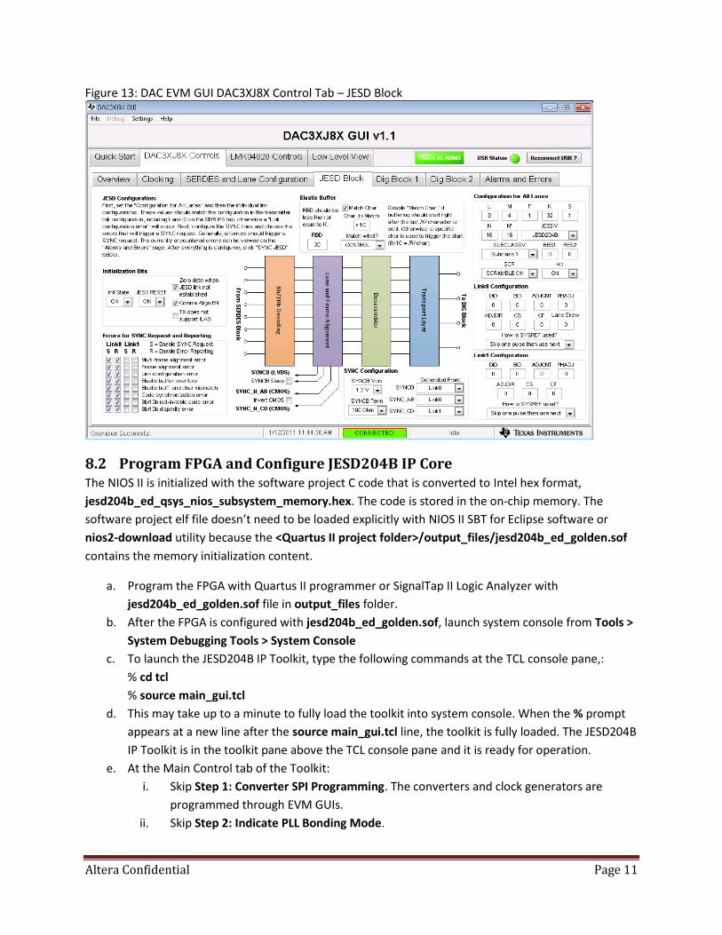
Figure 13: DAC EVM GUI DAC3XJ8X Control Tab – JESD Block
8.2 Program FPGA and Configure JESD204B IP Core The NIOS II is initialized with the software project C code that is converted to Intel hex format,
jesd204b_ed_qsys_nios_subsystem_memory.hex. The code is stored in the on-chip memory. The
software project elf file doesn’t need to be loaded explicitly with NIOS II SBT for Eclipse software or
nios2-download utility because the <Quartus II project folder>/output_files/jesd204b_ed_golden.sof
contains the memory initialization content.
a. Program the FPGA with Quartus II programmer or SignalTap II Logic Analyzer with
jesd204b_ed_golden.sof file in output_files folder.
b. After the FPGA is configured with jesd204b_ed_golden.sof, launch system console from Tools >
System Debugging Tools > System Console
c. To launch the JESD204B IP Toolkit, type the following commands at the TCL console pane,:
% cd tcl
% source main_gui.tcl
d. This may take up to a minute to fully load the toolkit into system console. When the % prompt
appears at a new line after the source main_gui.tcl line, the toolkit is fully loaded. The JESD204B
IP Toolkit is in the toolkit pane above the TCL console pane and it is ready for operation.
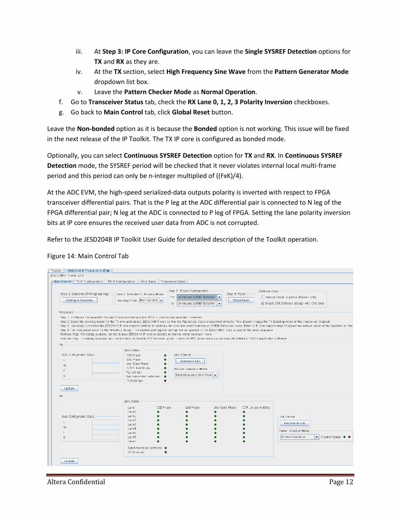
e. At the Main Control tab of the Toolkit:
i. Skip Step 1: Converter SPI Programming. The converters and clock generators are
programmed through EVM GUIs.
ii. Skip Step 2: Indicate PLL Bonding Mode.
Altera Confidential Page 12
iii. At Step 3: IP Core Configuration, you can leave the Single SYSREF Detection options for
TX and RX as they are.
iv. At the TX section, select High Frequency Sine Wave from the Pattern Generator Mode
dropdown list box.
v. Leave the Pattern Checker Mode as Normal Operation.
f. Go to Transceiver Status tab, check the RX Lane 0, 1, 2, 3 Polarity Inversion checkboxes.
g. Go back to Main Control tab, click Global Reset button.
Leave the Non-bonded option as it is because the Bonded option is not working. This issue will be fixed
in the next release of the IP Toolkit. The TX IP core is configured as bonded mode.
Optionally, you can select Continuous SYSREF Detection option for TX and RX. In Continuous SYSREF
Detection mode, the SYSREF period will be checked that it never violates internal local multi-frame
period and this period can only be n-integer multiplied of ((FxK)/4).
At the ADC EVM, the high-speed serialized-data outputs polarity is inverted with respect to FPGA
transceiver differential pairs. That is the P leg at the ADC differential pair is connected to N leg of the
FPGA differential pair; N leg at the ADC is connected to P leg of FPGA. Setting the lane polarity inversion
bits at IP core ensures the received user data from ADC is not corrupted.
Refer to the JESD204B IP Toolkit User Guide for detailed description of the Toolkit operation.
Figure 14: Main Control Tab
Altera Confidential Page 13
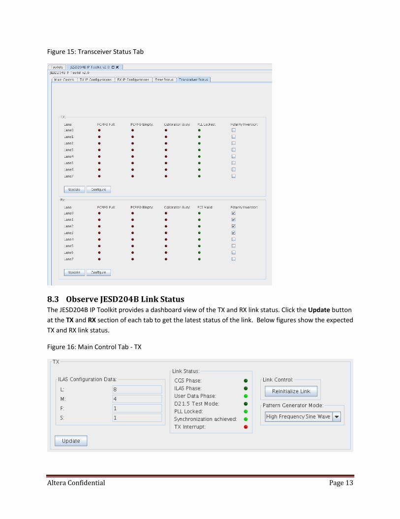
Figure 15: Transceiver Status Tab
8.3 Observe JESD204B Link Status The JESD204B IP Toolkit provides a dashboard view of the TX and RX link status. Click the Update button
at the TX and RX section of each tab to get the latest status of the link. Below figures show the expected
TX and RX link status.
Figure 16: Main Control Tab - TX
Altera Confidential Page 14
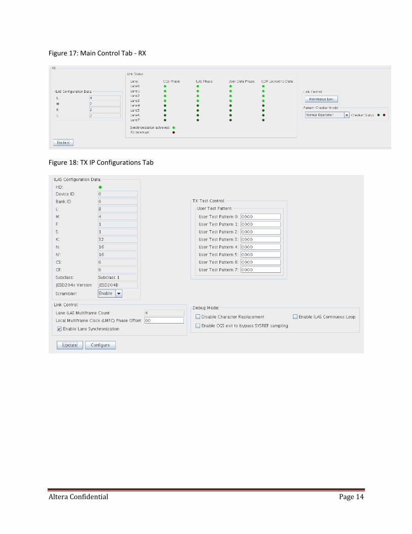
Figure 17: Main Control Tab - RX
Figure 18: TX IP Configurations Tab
Altera Confidential Page 15
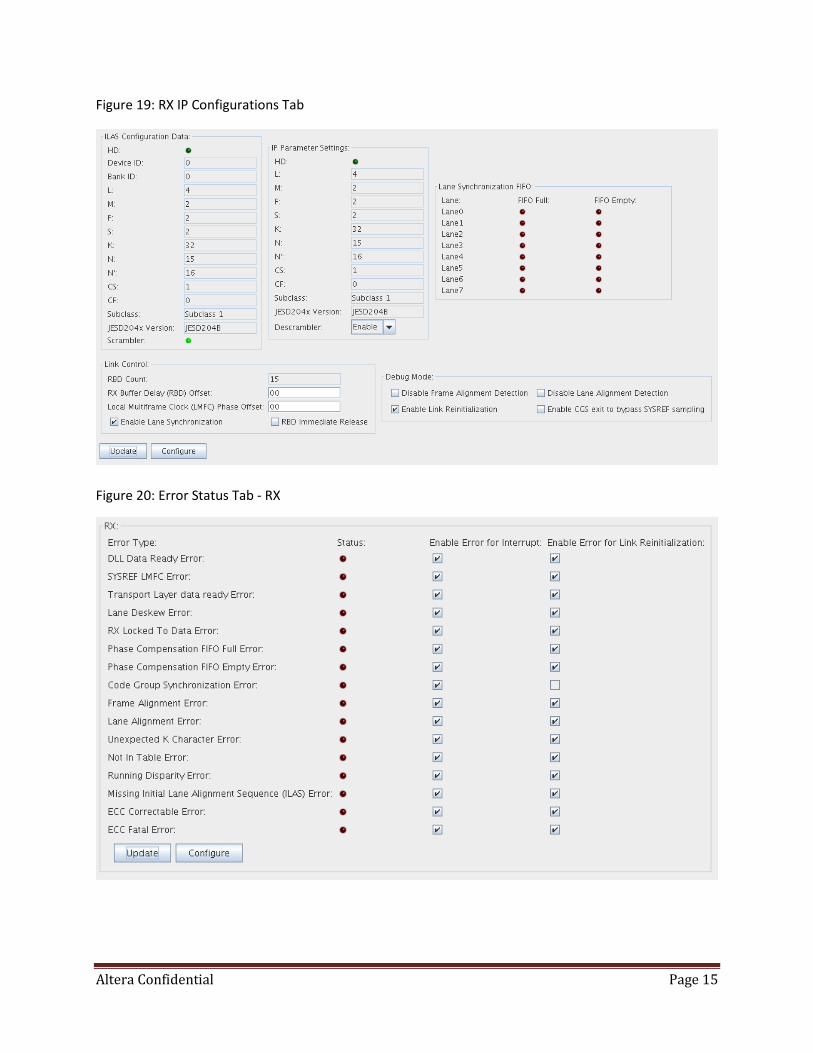
Figure 19: RX IP Configurations Tab
Figure 20: Error Status Tab - RX
Altera Confidential Page 16
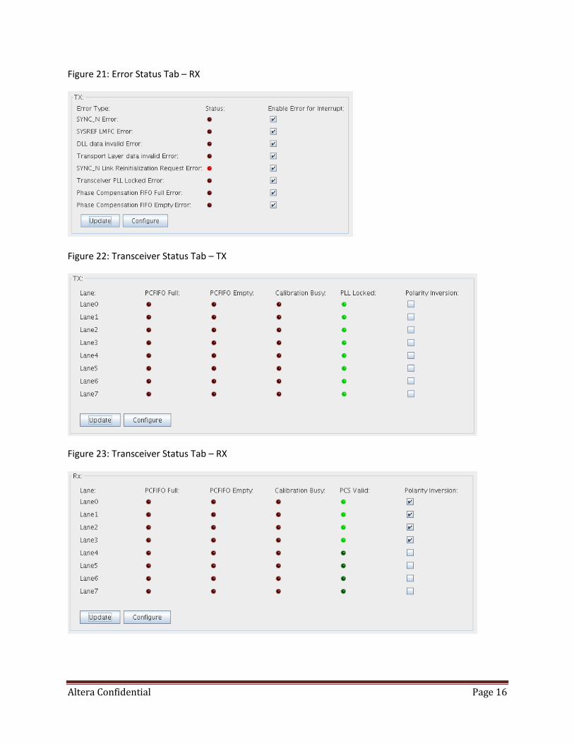
Figure 21: Error Status Tab – RX
Figure 22: Transceiver Status Tab – TX
Figure 23: Transceiver Status Tab – RX
Altera Confidential Page 17
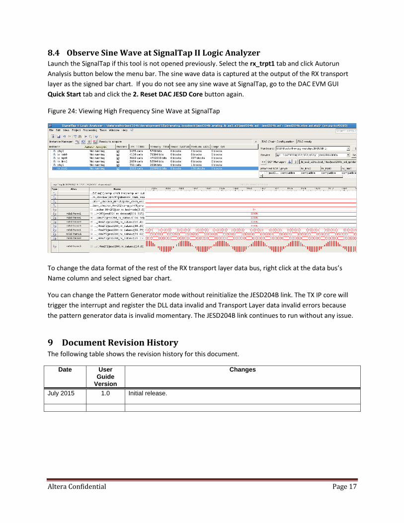
8.4 Observe Sine Wave at SignalTap II Logic Analyzer Launch the SignalTap if this tool is not opened previously. Select the rx_trpt1 tab and click Autorun
Analysis button below the menu bar. The sine wave data is captured at the output of the RX transport
layer as the signed bar chart. If you do not see any sine wave at SignalTap, go to the DAC EVM GUI
Quick Start tab and click the 2. Reset DAC JESD Core button again.
Figure 24: Viewing High Frequency Sine Wave at SignalTap
To change the data format of the rest of the RX transport layer data bus, right click at the data bus’s
Name column and select signed bar chart.
You can change the Pattern Generator mode without reinitialize the JESD204B link. The TX IP core will
trigger the interrupt and register the DLL data invalid and Transport Layer data invalid errors because
the pattern generator data is invalid momentary. The JESD204B link continues to run without any issue.
9 Document Revision History The following table shows the revision history for this document.
Date User Guide
Version
Changes
July 2015 1.0 Initial release.