Embed Size (px)
Citation preview
1
ALTERA Technical Papers
2
Contents
I. Programmable Logic Increases Bandwidth and Adaptability in Communications Equipment ...............7 II. Managing Power in High Speed Programmable Logic.......................................................................... 11
Abstract .................................................................................................................................................. 11 1. Introduction........................................................................................................................................ 11 2. The Components of Power Consumption .......................................................................................... 11 3. Estimating Power Consumption.........................................................................................................12
3.1 Standby Power ............................................................................................................................12 3.2 Internal Power.............................................................................................................................13 3.3 External Power ...........................................................................................................................13
4. Managing Power in Programmable Logic .........................................................................................14 4.1 Automatic Power-Down .............................................................................................................14 4.2 Programmable Speed/Power Control .........................................................................................14 4.3 Pin-Controlled Power Down.......................................................................................................15 4.4 3.3-volt Devices..........................................................................................................................15 4.5 3.3-Volt / 5.0-Volt Hybrid Devices .............................................................................................16
Conclusion .............................................................................................................................................17 III. PLD Based FFTs ....................................................................................................................................18
Abstract ..................................................................................................................................................18 1. Introduction........................................................................................................................................18 2. FFT Megafunctions............................................................................................................................18 3. Altera FLEX 10K PLDs.....................................................................................................................19 4. Performance Data...............................................................................................................................20 5. Discussion ..........................................................................................................................................21 Conclusions............................................................................................................................................22
IV. The Library of Parameterized Modules (LPM)......................................................................................23
Introduction............................................................................................................................................23 1. The History of LPM...........................................................................................................................23 2. The Objective of LPM .......................................................................................................................24
2.1 Allow Technology-Independent Design Entry............................................................................24 2.2 Allow Efficient Design Mapping................................................................................................24 2.3 Allow Tool-Independent Design Entry .......................................................................................24 2.4 Allow specification of a complete design ...................................................................................24
3. The LPM Functions............................................................................................................................24 4. Design Flow with LPM......................................................................................................................25 5. Efficient Technology Mapping...........................................................................................................26 6. The Future of LPM.............................................................................................................................27 Conclusion .............................................................................................................................................28
V. A Programmable Logic Design Approach to Implementing PCI Interfaces ..........................................30
1. Customizable Functionality ...............................................................................................................30 2. Description of PCI Macrofunctions ...................................................................................................30 3. Brief Introduction to AHDL...............................................................................................................31 4. Modifying/Customizing the Macrofunctions .....................................................................................33 5. Adjusting the Width of Address/Data Buses ......................................................................................34 6. Other Customizations.........................................................................................................................37 7. Hardware Implementation..................................................................................................................37 Conclusion .............................................................................................................................................39
3
Obtaining the Macrofunctions ..........................................................................................................39 VI. Altera’s PCI MegaCore Solution ...........................................................................................................40 VII. A VHDL Design Approach to a Master/Target PCI Interface................................................................43
ABSTRACT...........................................................................................................................................43 1. INTRODUCTION .............................................................................................................................43 2. ARCHITECTURE CONSIDERATIONS ..........................................................................................44
2.1 Performance................................................................................................................................44 2.2 Interoperability ...........................................................................................................................45 2.3 Vendor Independence..................................................................................................................45 2.4 Design cycle ...............................................................................................................................45
3. System Methodology .........................................................................................................................45 3.1 Hardware Selection.....................................................................................................................45 3.2 Design Entry ...............................................................................................................................45 3.3 PLD Selection.............................................................................................................................46 3.3 EDA tool selection......................................................................................................................46
4. IMPLEMENTATION.........................................................................................................................46 4.1 Implementing Functionality........................................................................................................46 4.2 Implementing Burst Mode..........................................................................................................47
5. PCI EXPERIENCE ............................................................................................................................47 6. FUTURE ROADMAP.......................................................................................................................48 Conclusion .............................................................................................................................................49
Author biographies ...........................................................................................................................49 VIII. Interfacing a PowerPC 403GC to a PCI Bus ....................................................................................50
Introduction............................................................................................................................................50 Conclusion .............................................................................................................................................59
References ........................................................................................................................................59 IX. HIGH PERFORMANCE DSP SOLUTIONS IN ALTERA CPLDS .....................................................60
INTRODUCTION .................................................................................................................................60 1. HIGH PERFORMANCE DSP...........................................................................................................60 2. VECTOR PROCESSING: An Alternative ‘MAC’ Architecture........................................................61
2.1 LOOK-UP TABLE (LUT) BASED ARCHITECTURE.............................................................62 3. FIR FILTERS USING VECTOR MULTIPLIERS.............................................................................65 4. IMAGE PROCESSING USING VECTOR MULTIPLIERS.............................................................66
4.1 OPTIMISED DCT FOR USE IN FLEX10K..............................................................................66 5. FAST FOURIER TRANSFORMS (FFTs).........................................................................................68 CONCLUSION......................................................................................................................................70
REFERENCES.................................................................................................................................70 X. Enhance The Performance of Fixed Point DSP Processor Systems.......................................................71
Introduction............................................................................................................................................71 1. DSP Design Options...........................................................................................................................71 2. The Application of Programmable Logic...........................................................................................72 3. Arithmetic Capability of Programmable Logic..................................................................................73 4. FIR Filters in PLDs............................................................................................................................74 5. Using the Vector Multiplier in FIR Filters .........................................................................................78 6. Case Studies of PLDs used as DSP Coprocessors..............................................................................79 7. System Implementation Recommendations .......................................................................................83
XI. HDTV Rate Image Processing on the Altera FLEX 10K.......................................................................84
Introduction............................................................................................................................................84
4
1. Altera FLEX 10K Architecture ..........................................................................................................85 2. Megafunction Development...............................................................................................................87 3. Image Processing Megafunctions ......................................................................................................87 Conclusions............................................................................................................................................89
XII. Automated Design Tools for Adaptive Filter Development...................................................................90
Introduction............................................................................................................................................90 1. Filter Building Blocks........................................................................................................................90 2. Filter Design and Implementation......................................................................................................91 3. Transversal Filters ..............................................................................................................................93 4. LPM Implementation Examples ........................................................................................................93 Conclusions............................................................................................................................................95
References ........................................................................................................................................95 XIII. Building FIR Filters in LUT-Based Programmable Logic ...............................................................96
Introduction............................................................................................................................................96 1. LUT-Based PLD Architecture............................................................................................................96 2. FIR Filter Architecture .......................................................................................................................97 3. Parallel FIR Filter Performance .......................................................................................................101 4. Serial FIR Filters..............................................................................................................................102 5. Serial Filter Performance and Resource Utilization.........................................................................103 6. Pipelining .........................................................................................................................................104 7. FIR Filter Precision (Input Bit Width and Number of Taps)............................................................104 8. LUT-Based PLDs as DSP Coprocessors ..........................................................................................105
XIV. Automated FFT Processor Design..................................................................................................106
Abstract ................................................................................................................................................106 1. INTRODUCTION ...........................................................................................................................106 2. FFT DESIGN ...................................................................................................................................106 3. FFT PARAMETERS........................................................................................................................107 4. FFT PROCESSOR ARCHITECTURE............................................................................................107 5. FFT IMPLEMENTATION...............................................................................................................108 6. FFT DESIGN CONSIDERATIONS................................................................................................109
6.1 Prime FFT Decomposition .......................................................................................................109 6.2 CORDIC FFT Core...................................................................................................................109 6.3 Higher Radix............................................................................................................................. 110
7. IFFT PROCESSING........................................................................................................................ 110 8. HIGHER PERFORMANCE FFTs................................................................................................... 110 CONCLUSIONS.................................................................................................................................. 112
REFERENCES............................................................................................................................... 112 XV. Implementing an ATM Switch Using Megafunctions Optimized for Programmable Logic................ 113
1. ATM Background............................................................................................................................. 113 2. ATM Megafunction Blocks .............................................................................................................. 116 3. Utilization of Embedded Array Blocks ............................................................................................ 116 4. Logic Cell Usage.............................................................................................................................. 117 5. Applications ..................................................................................................................................... 117
XVI. Incorporating Phase-Locked Loop Technology into Programmable Logic Devices ...................... 118
1. ClockLock and ClockBoost Features in FLEX 10K and MAX 7000S............................................ 118 2. Specifying ClockLock and ClockBoost Usage in MAX+PLUS II .................................................. 118 3. Details of ClockLock Usage ............................................................................................................120 4. Timing Analysis ...............................................................................................................................121 5. Delay Matrix ....................................................................................................................................121
5
6. Setup/Hold Matrix............................................................................................................................122 7. Registered Performance ...................................................................................................................122 8. Simulation ........................................................................................................................................122 9. ClockLock Status .............................................................................................................................123 10. System Startup Issues.....................................................................................................................124 11. Multi-clock System Issues .............................................................................................................125
11.1 Case 1......................................................................................................................................126 11.2 Case 2......................................................................................................................................126
12. ClockLock and ClockBoost Specifications....................................................................................127 13. Duty Cycle .....................................................................................................................................128 14. Clock Deviation .............................................................................................................................128 15. Clock Stability................................................................................................................................128 16. Lock Time ......................................................................................................................................128 17. Jitter................................................................................................................................................128 18. Clock Delay....................................................................................................................................128 19. Board Layout..................................................................................................................................129 Conclusion ...........................................................................................................................................131
References ......................................................................................................................................131 XVII. Implementation of a Digital Receiver for Narrow Band Communications Applications. ..............132
Abstract ................................................................................................................................................132 1. Introduction......................................................................................................................................132 2. Digital IF Receiver architecture. ......................................................................................................132
2.1 PLD Baseband processing functions ........................................................................................133 3. PLD design approach. ......................................................................................................................134 4. PLD Implementation........................................................................................................................134
4.1 Matched Filters .........................................................................................................................134 4.2 Timing Estimator ......................................................................................................................134 4.3 Interpolators..............................................................................................................................135 4.4 Decimators................................................................................................................................136 4.5 PLD partitioning.......................................................................................................................136
5. Logic Synthesis ................................................................................................................................136 6. BER performance and implementation loss.....................................................................................138 Conclusions..........................................................................................................................................139
References ......................................................................................................................................139 XVIII. Image Processing in Altera FLEX 10K Devices ............................................................................140
Introduction..........................................................................................................................................140 1. Why Use Programmable Logic? ......................................................................................................140 2. Altera FLEX 10K CPLD..................................................................................................................140 3. Image Transform Examples .............................................................................................................141
3.1 Walsh Transform.......................................................................................................................141 3.2 Discrete Cosine Transform .......................................................................................................142 3.3 Implementation.........................................................................................................................144
4. Filters in FLEX Devices...................................................................................................................146 Conclusion ...........................................................................................................................................148
References ......................................................................................................................................148 XIX. The Importance of JTAG and ISP in Programmable Logic............................................................149
1. Packaging, Flexibility Drive In-System Programmability Adoption ...............................................149 2. Prototyping Flexibility .....................................................................................................................149 3. ISP Benefits to Manufacturing.........................................................................................................150 4. Decreasing Board Size, Increasing Complexity Drive Adoption of JTAG Boundary Scan..........150 5. JTAG Defined ..................................................................................................................................150

6
6. MAX 9000 Combines ISP and JTAG ..............................................................................................151 Author Biography ................................................................................................................................152
XX. Reed Solomon Codec Compiler for Programmable Logic ..................................................................153
1. INTRODUCTION ...........................................................................................................................153 2. PARAMETERS................................................................................................................................153
2.1 TOTAL NUMBER OF SYMBOLS PER CODEWORD .........................................................153 2.2 NUMBER OF CHECK SYMBOLS.........................................................................................153 2.3 NUMBER OF BITS PER SYMBOL .......................................................................................153 2.4 IRREDUCIBLE FIELD POLYNOMIAL.................................................................................153 2.5 FIRST ROOT OF THE GENERATOR POLYNOMIAL.........................................................154
3. DESIGN FLOW...............................................................................................................................154 4. RESOURCE REQUIREMENTS.....................................................................................................154 5. CALCULATING SYSTEM PERFORMANCE...............................................................................155
5.1 DISCRETE DECODER ...........................................................................................................155 5.2 STREAMING DECODER .......................................................................................................156
CONCLUSIONS..................................................................................................................................158 REFERENCES...............................................................................................................................158
7
I. Programmable Logic Increases Bandwidth and Adaptability in
Communications Equipment
Robert K. Beachler Manager, Strategic Marketing and Communications
Altera Corporation The transmission and distribution of information, called communications, is a cornerstone in today's information age. The networking of computers is still in its infancy, and possibilities for worldwide computing and transmission of information are just beginning to be explored. As not only the business user, but the home user as well, develops a taste for real-time, worldwide access of information, the demand for communications services will increase. Therefore, the bandwidth of communications equipment will need to undergo tremendous increases in order to keep up with the demands of corporations and home users. Companies that develop communications products, such as LANs, WANs, bridges, routers, hubs, and PBX systems, are continually striving to increase the amount of information that can be transmitted, and to increase the speed of transmission. A pivotal portion of this engineering task is the development of efficient switching and scheduling algorithms for the steering of data through complex systems. Due to the performance requirements of information transmittal, communications designs are implemented in fixed silicon solutions, offering high-performance for a defined set of data packet and loading requirements. However, network traffic, loading, and even the basic data structures of information may change over time, and these fixed solutions then become less optimal and must be replaced. Programmable logic has been used extensively in the communications sector due to its unique combination of speed and flexibility, enabling engineers designing communications systems to rapidly produce new products which address shifting communications standards and system requirements. However, the onslaught of new communications products does not address two important issues facing communications systems. First, for the MIS manager and service provider, new products are problematic in that they do not protect existing investments in high-priced hardware. MIS managers wish to preserve their investments in communications equipment and would prefer to have their systems be upgraded as demand increases and new technologies become available, rather than installing entirely new systems. Secondly, these new products do little to alleviate the near-term difficulty of adapting real-time to changing networking needs. Reprogrammable logic device may help to mitigate these nagging problems. PLDs can facilitate the smooth migration of new technologies, such as ATM, into existing systems, while also addressing the time-to-market concerns of network providers. Re-configurable SRAM-based programmable logic devices provide the means to implement adaptable communications hardware which can be automatically configured to implement today's communications standards, such as Ethernet, and simply re-configured, in real time, to adapt to emerging communications standards such as 25 Mbps Desktop ATM. In-Circuit Reconfigurability holds promise to solve not only the investment issue of the MIS manager, but also address the performance aspects of switching systems. If system requirements change or traffic patterns fluctuate, PLDs allow the designer to change the characteristics of the switch in the field. This allows for tailoring the switch to meet the changing needs of the environment. The loading of networks is a dynamic problem with many factors affecting the performance. These include number of users, data sizes being transmitted, peak vs. off-peak usage, protocol used, and the possibility of physical connection interruption. These factors make modeling and simulating throughput a difficult problem. This then begs the question of how to develop an optimally performing communications system when only the boundary conditions, and not the actual conditions are known. The creation of hardware prototypes using programmable logic is quite helpful in exploring the possibilities and tuning the system.
8
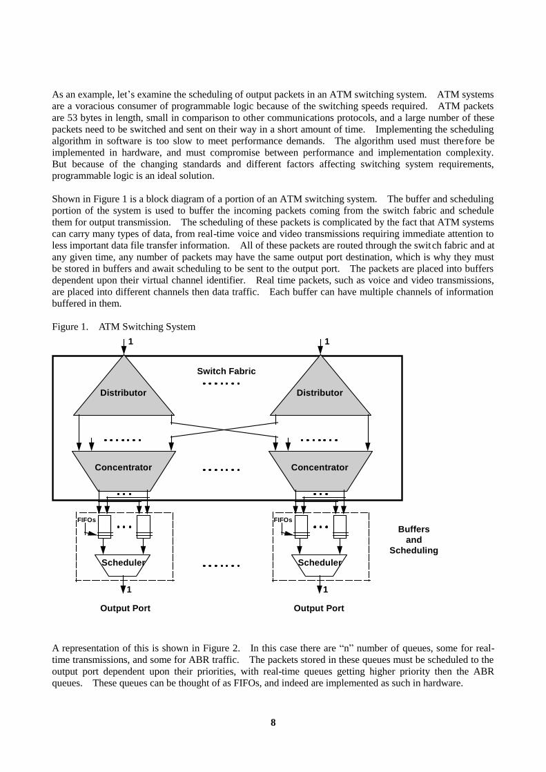
As an example, let’s examine the scheduling of output packets in an ATM switching system. ATM systems are a voracious consumer of programmable logic because of the switching speeds required. ATM packets are 53 bytes in length, small in comparison to other communications protocols, and a large number of these packets need to be switched and sent on their way in a short amount of time. Implementing the scheduling algorithm in software is too slow to meet performance demands. The algorithm used must therefore be implemented in hardware, and must compromise between performance and implementation complexity. But because of the changing standards and different factors affecting switching system requirements, programmable logic is an ideal solution. Shown in Figure 1 is a block diagram of a portion of an ATM switching system. The buffer and scheduling portion of the system is used to buffer the incoming packets coming from the switch fabric and schedule them for output transmission. The scheduling of these packets is complicated by the fact that ATM systems can carry many types of data, from real-time voice and video transmissions requiring immediate attention to less important data file transfer information. All of these packets are routed through the switch fabric and at any given time, any number of packets may have the same output port destination, which is why they must be stored in buffers and await scheduling to be sent to the output port. The packets are placed into buffers dependent upon their virtual channel identifier. Real time packets, such as voice and video transmissions, are placed into different channels then data traffic. Each buffer can have multiple channels of information buffered in them. Figure 1. ATM Switching System
Scheduler
FIFOs
Concentrator
1
Distributor
1
Scheduler
FIFOs
Concentrator
1
Distributor
1
Switch Fabric
Buffersand
Scheduling
Output Port Output Port
A representation of this is shown in Figure 2. In this case there are “n” number of queues, some for real-time transmissions, and some for ABR traffic. The packets stored in these queues must be scheduled to the output port dependent upon their priorities, with real-time queues getting higher priority then the ABR queues. These queues can be thought of as FIFOs, and indeed are implemented as such in hardware.
9
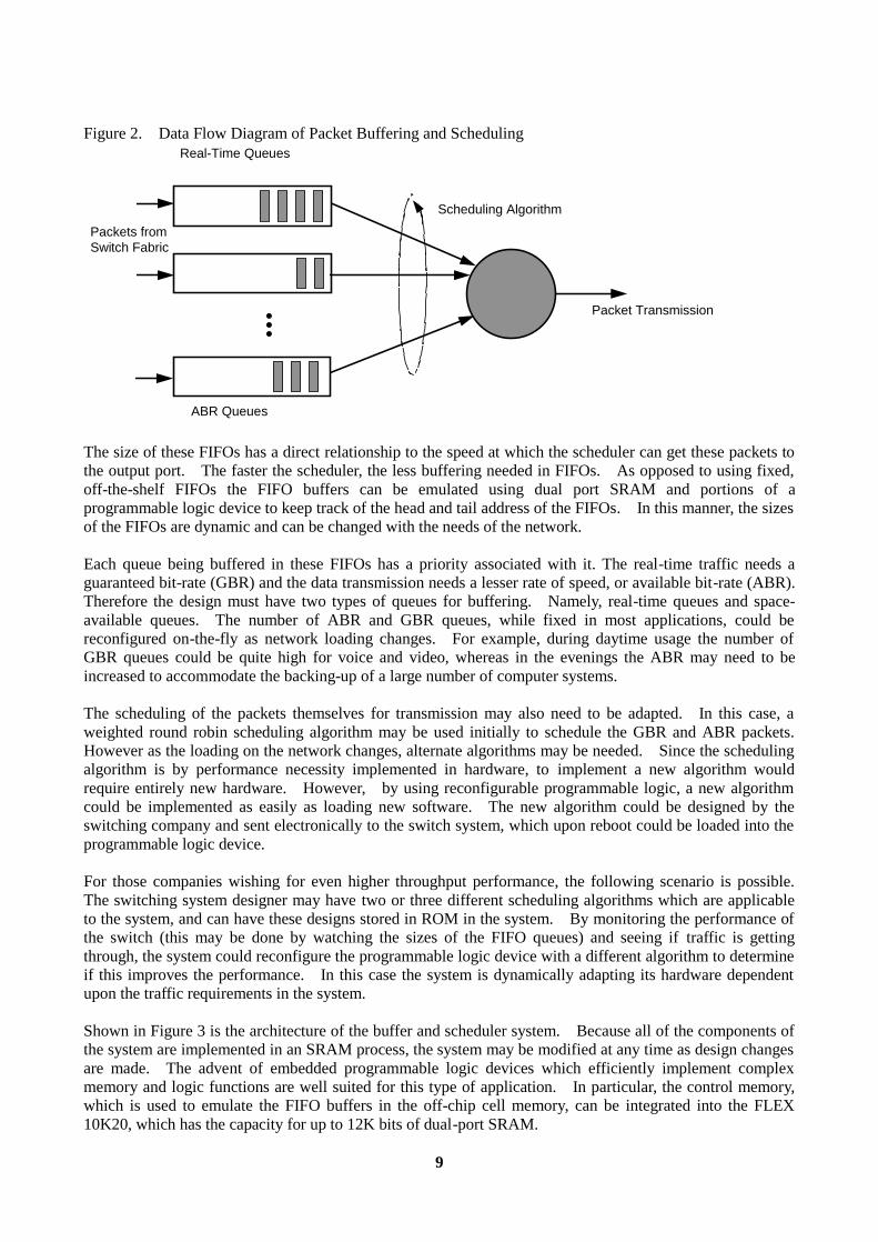
Figure 2. Data Flow Diagram of Packet Buffering and Scheduling
Packet Transmission
Scheduling Algorithm
Real-Time Queues
ABR Queues
Packets fromSwitch Fabric
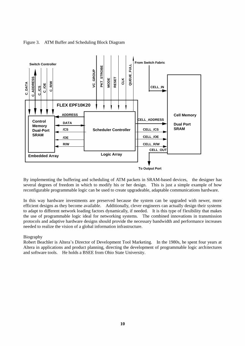
The size of these FIFOs has a direct relationship to the speed at which the scheduler can get these packets to the output port. The faster the scheduler, the less buffering needed in FIFOs. As opposed to using fixed, off-the-shelf FIFOs the FIFO buffers can be emulated using dual port SRAM and portions of a programmable logic device to keep track of the head and tail address of the FIFOs. In this manner, the sizes of the FIFOs are dynamic and can be changed with the needs of the network. Each queue being buffered in these FIFOs has a priority associated with it. The real-time traffic needs a guaranteed bit-rate (GBR) and the data transmission needs a lesser rate of speed, or available bit-rate (ABR). Therefore the design must have two types of queues for buffering. Namely, real-time queues and space-available queues. The number of ABR and GBR queues, while fixed in most applications, could be reconfigured on-the-fly as network loading changes. For example, during daytime usage the number of GBR queues could be quite high for voice and video, whereas in the evenings the ABR may need to be increased to accommodate the backing-up of a large number of computer systems. The scheduling of the packets themselves for transmission may also need to be adapted. In this case, a weighted round robin scheduling algorithm may be used initially to schedule the GBR and ABR packets. However as the loading on the network changes, alternate algorithms may be needed. Since the scheduling algorithm is by performance necessity implemented in hardware, to implement a new algorithm would require entirely new hardware. However, by using reconfigurable programmable logic, a new algorithm could be implemented as easily as loading new software. The new algorithm could be designed by the switching company and sent electronically to the switch system, which upon reboot could be loaded into the programmable logic device. For those companies wishing for even higher throughput performance, the following scenario is possible. The switching system designer may have two or three different scheduling algorithms which are applicable to the system, and can have these designs stored in ROM in the system. By monitoring the performance of the switch (this may be done by watching the sizes of the FIFO queues) and seeing if traffic is getting through, the system could reconfigure the programmable logic device with a different algorithm to determine if this improves the performance. In this case the system is dynamically adapting its hardware dependent upon the traffic requirements in the system. Shown in Figure 3 is the architecture of the buffer and scheduler system. Because all of the components of the system are implemented in an SRAM process, the system may be modified at any time as design changes are made. The advent of embedded programmable logic devices which efficiently implement complex memory and logic functions are well suited for this type of application. In particular, the control memory, which is used to emulate the FIFO buffers in the off-chip cell memory, can be integrated into the FLEX 10K20, which has the capacity for up to 12K bits of dual-port SRAM.
10
Figure 3. ATM Buffer and Scheduling Block Diagram
CELL_IN
CELL_ADDRESS
CELL_/CS
CELL_/OE
CELL_OUT
CELL_R/W
From Switch Fabric
ADDRESS
DATA
/CS
/OE
R/W
C_A
DD
RES
S
VC_G
RO
UP
PKT_
STR
OB
E
MO
DE
RES
ET
CLK
QU
EUE_
FULL
C_D
ATA
C_/
CS
C_R
/W
C_/
OE
To Output Port
ControlMemoryDual-PortSRAM
Cell Memory
Dual Port SRAM
Logic Array
Switch Controller
Embedded Array
FLEX EPF10K20
Scheduler Controller
By implementing the buffering and scheduling of ATM packets in SRAM-based devices, the designer has several degrees of freedom in which to modify his or her design. This is just a simple example of how reconfigurable programmable logic can be used to create upgradeable, adaptable communications hardware. In this way hardware investments are preserved because the system can be upgraded with newer, more efficient designs as they become available. Additionally, clever engineers can actually design their systems to adapt to different network loading factors dynamically, if needed. It is this type of flexibility that makes the use of programmable logic ideal for networking systems. The combined innovations in transmission protocols and adaptive hardware designs should provide the necessary bandwidth and performance increases needed to realize the vision of a global information infrastructure. Biography Robert Beachler is Altera’s Director of Development Tool Marketing. In the 1980s, he spent four years at Altera in applications and product planning, directing the development of programmable logic architectures and software tools. He holds a BSEE from Ohio State University.

11
II. Managing Power in High Speed Programmable Logic
Craig Lytle, Director of Product Planning and Applications
Altera Corporation
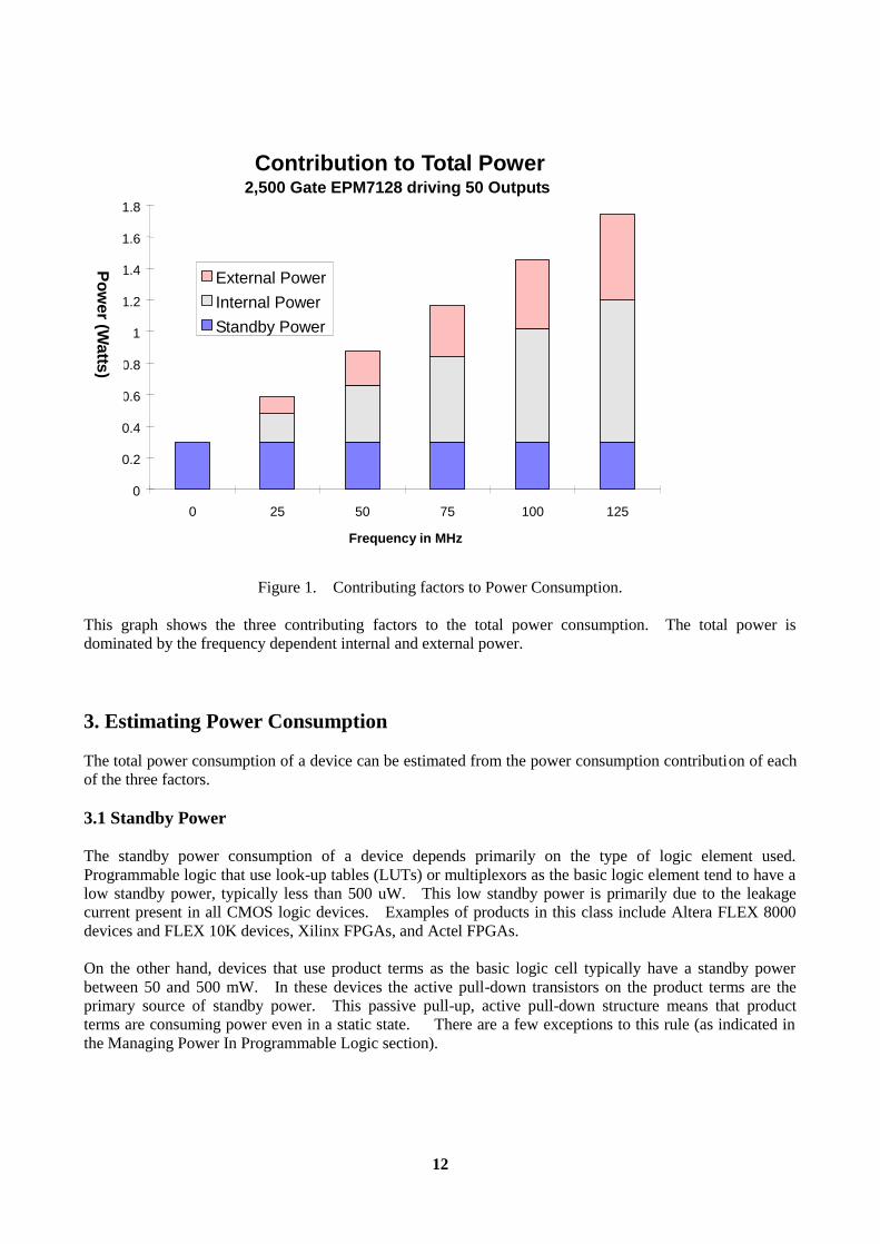
Abstract This paper describes techniques to manage the power consumption of high-speed programmable logic devices (PLDs). Power consumption has become an increasingly important issue to system designers as the speed (and thus power consumption) of programmable logic devices has increased. To address power consumption concerns, design engineers need to accurately predict the power conumption of a design before the design is implemented on the board. When power consumption is too high, there are many design approaches and device features that can reduce the ultimate power consumption of the design. 1. Introduction Since power is a direct function of operating frequency, power consumption has become a greater issue as system performance has increased. Initially the concern of only the few designers working on portable equipment, power consumption is now important to a growing number of design engineers working on everything from PC add-on cards to telecom equipment. In logic ICs, power consumption is a direct function of factors such as gate count, operating frequency, and pin count. As these fundamental metrics of the logic semiconductor industry continue to grow, power consumption will grow as well. Fortunately for power-conscious designers, several PLDs offer options to reduce power consumption. These features, along with an eventual migration to 3.3-volt devices will keep power consumption issues manageable. 2. The Components of Power Consumption The total power consumed by a PLD is made up of three major components: standby, internal, and external. An equation for total power (PTOTAL), shown below, reflects these three contributions: PTOTAL = PSTANDBY + PINTERNAL+ PEXTERNAL Where: PSTANDBY is the standby power consumed by the powered device when no inputs are toggling. PINTERNAL is the power associated with the active internal circuitry and is a function of the clock frequency. PEXTERNAL is the power associated with driving the output signals and is a function of the number of outputs, the output load, and the output toggle frequency. Figure 1 shows the power consumption of a 2,500-gate PLD broken down into PSTANDBY, PINTERNAL, and PEXTERNAL. As indicated in the figure, power consumption is strong function of frequency, and the internal and external power consumption are large contributors at the frequencies typically found in today’s systems. The standby power is a significant factor only at low frequencies.
12
Contribution to Total Power2,500 Gate EPM7128 driving 50 Outputs
0
0.2
0.4
0.6
0.8
1
1.2
1.4
1.6
1.8
0 25 50 75 100 125
Frequency in MHz
External PowerInternal PowerStandby Power
Power (W
atts)
Figure 1. Contributing factors to Power Consumption. This graph shows the three contributing factors to the total power consumption. The total power is dominated by the frequency dependent internal and external power. 3. Estimating Power Consumption The total power consumption of a device can be estimated from the power consumption contribution of each of the three factors. 3.1 Standby Power The standby power consumption of a device depends primarily on the type of logic element used. Programmable logic that use look-up tables (LUTs) or multiplexors as the basic logic element tend to have a low standby power, typically less than 500 uW. This low standby power is primarily due to the leakage current present in all CMOS logic devices. Examples of products in this class include Altera FLEX 8000 devices and FLEX 10K devices, Xilinx FPGAs, and Actel FPGAs. On the other hand, devices that use product terms as the basic logic cell typically have a standby power between 50 and 500 mW. In these devices the active pull-down transistors on the product terms are the primary source of standby power. This passive pull-up, active pull-down structure means that product terms are consuming power even in a static state. There are a few exceptions to this rule (as indicated in the Managing Power In Programmable Logic section).

13
3.2 Internal Power The internal power consumption of programmable logic devices is due to the switching of signals within the device. Each time a signal is raised and lowered, current flows into and out of the device, thereby increasing the power consumption. To help engineers estimate the internal power consumption of their designs, most PLD vendors publish equations or graphs that estimate the internal current consumption of a device as a function of the operating frequency and the resource utilization of the device. For example, the following equation is used to estimate the internal current consumption of Altera’s FLEX 8000 devices: IINTERNAL = KFNp. In this equation, K is a constant equal to 75 uA/MHz/LE, meaning that each logic element (LE) consumes 75 uA for each full cycle transition. F is the master system frequency, N is the number of LEs, and p is the percentage of LEs that toggle on each clock edge. A conservative estimate for p is 12.5% (0.125). Using this equation reveals that a 2,500-gate design (200 logic elements) running at 50 MHz will consume approximately 93 mA, or 468 mW, due to internal circuitry. 3.3 External Power The external power consumed is dependent on only two main factors: the output load and the output toggle frequency. Because both of these factors are independent of the device type, the external power consumption is dependent entirely on the design, not the device. A good approach to estimating external power is to use the following equation: PEXTERNAL = 1/2 ∑ Cn Fn Vn
2. In this equation Cn is the capacitive load of output pin n, Fn is the toggle frequency of pin n, and Vn
2 is the voltage swing of pin n. Assuming that C, F, and V is the same for each pin, the equation simplifies to: PEXTERNAL = 1/2 ACpF V2, where A is the number of outputs, C is the average load, F is the system frequency, and V is the average voltage swing. The factor p is the estimated number of clock cycles that an output pin toggles. A conservative estimate for p is 20% (0.2). Currently, most PLDs drive TTL output voltages with an NMOS pull-up transistor. Using an NMOS instead of PMOS transistor makes the voltage swing approximately 3.8 volts, rather than the full 5.0-volt rail. Devices with CMOS output drive options or internal pull-up resistors have a higher output voltage and significantly higher power consumption. Output switching contributes significantly to the power consumption of an application, regardless of the device chosen. For example, a 50-MHz application with 50 output pins driving 35-pF loads would consume approximately 126 mW of power, as shown in the following equation: PEXTERNAL = 1/2 (50 pins)(35 pF/pin) (20%)(50 MHz)(3.8 V)2 = 126 mW.

14
4. Managing Power in Programmable Logic There are several approaches to managing power consumption in programmable logic. The easiest approach is to take advantage of the power consumption features offered by many programmable logic devices. Switching to 3.3-volt PLDs is another option. Programmable logic devices that run at 3.3 volts are now available from a few vendors, with more to come in the near future. In the mean time, 3.3V/5.0V hybrid devices are the perfect choice for designers who need to use components that require both power supply standards. Many of the programmable logic devices available today have features that can be used to manage power consumption, including automatic power-down, programmable speed/power control, and pin-controlled power down. Different applications benefit from different approaches to power consumption management. The following descriptions of the different approaches and their impact on power consumption can help you choose the features that are appropriate for your application. 4.1 Automatic Power-Down To reduce standby power consumption, some EPROM-based PLDs offer an automatic power-down feature. These devices contain internal power-down circuitry that continually monitors the inputs and internal signals of a device, and powers down the internal EPROM array after approximately 100 ns of inactivity. When an input changes, the EPROM array is then powered up and the device behaves as normal. For example, Altera Classic devices offer a power-down feature (called the "zero-power mode") enabled and disabled. The zero-power mode eliminates the power consumed by the product-terms, reducing the standby power consumption to that consumed by CMOS leakage current. 4.2 Programmable Speed/Power Control Some programmable devices allow the designer to trade off between speed and power. Since many applications have only a few truly speed-critical paths, a designer can choose to run parts of the design at high speed while the rest of the design runs at low power. For designers that require high speed in at least some portion of their design, this feature may provide the most effective means of managing power consumption. For example, with MAX 7000 and MAX 9000 devices, each macrocell can be programmed by the designer to operate in the turbo mode or low-power mode. The turbo mode offers higher performance with normal power consumption, while the low-power mode offers reduced power consumption with lower performance. The low-power mode reduces the macrocell's power consumption by 50% while increasing the delay by 7-15 ns, depending on the speed grade. Figure 2 shows the power consumed by an Altera MAX 7000 device under two conditions: one in which the turbo mode is turned on for all macrocells in the device, and one in which the low-power mode options are turned on for all the macrocells in the device. The actual power consumed by a design would lie between the two lines depending on how many macrocells are set in each mode.
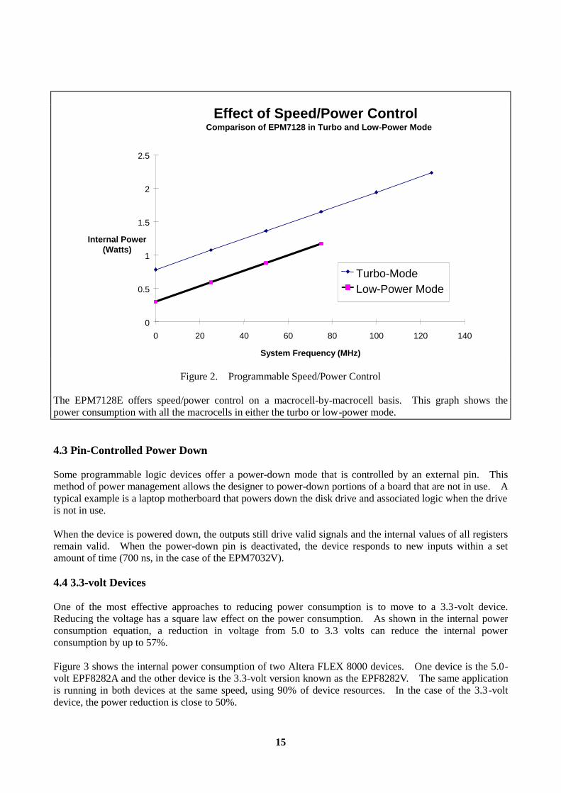
15
Effect of Speed/Power ControlComparison of EPM7128 in Turbo and Low-Power Mode
0
0.5
1
1.5
2
2.5
0 20 40 60 80 100 120 140
System Frequency (MHz)
Internal Power(Watts)
Turbo-ModeLow-Power Mode
Figure 2. Programmable Speed/Power Control The EPM7128E offers speed/power control on a macrocell-by-macrocell basis. This graph shows the power consumption with all the macrocells in either the turbo or low-power mode. 4.3 Pin-Controlled Power Down Some programmable logic devices offer a power-down mode that is controlled by an external pin. This method of power management allows the designer to power-down portions of a board that are not in use. A typical example is a laptop motherboard that powers down the disk drive and associated logic when the drive is not in use. When the device is powered down, the outputs still drive valid signals and the internal values of all registers remain valid. When the power-down pin is deactivated, the device responds to new inputs within a set amount of time (700 ns, in the case of the EPM7032V). 4.4 3.3-volt Devices One of the most effective approaches to reducing power consumption is to move to a 3.3-volt device. Reducing the voltage has a square law effect on the power consumption. As shown in the internal power consumption equation, a reduction in voltage from 5.0 to 3.3 volts can reduce the internal power consumption by up to 57%. Figure 3 shows the internal power consumption of two Altera FLEX 8000 devices. One device is the 5.0-volt EPF8282A and the other device is the 3.3-volt version known as the EPF8282V. The same application is running in both devices at the same speed, using 90% of device resources. In the case of the 3.3-volt device, the power reduction is close to 50%.
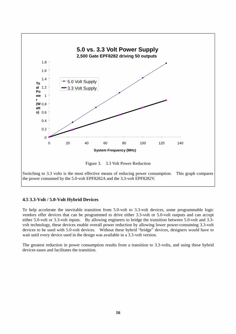
16
5.0 vs. 3.3 Volt Power Supply2,500 Gate EPF8282 driving 50 outputs
0
0.2
0.4
0.6
0.8
1
1.2
1.4
1.6
1.8
0 20 40 60 80 100 120 140
System Frequency (MHz)
ToalPower(Watts)
5.0 Volt Supply3.3 Volt Supply
Figure 3. 3.3 Volt Power Reduction Switching to 3.3 volts is the most effective means of reducing power consumption. This graph compares the power consumed by the 5.0-volt EPF8282A and the 3.3-volt EPF8282V. 4.5 3.3-Volt / 5.0-Volt Hybrid Devices To help accelerate the inevitable transition from 5.0-volt to 3.3-volt devices, some programmable logic vendors offer devices that can be programmed to drive either 3.3-volt or 5.0-volt outputs and can accept either 5.0-volt or 3.3-volt inputs. By allowing engineers to bridge the transition between 5.0-volt and 3.3-volt technology, these devices enable overall power reduction by allowing lower power-consuming 3.3-volt devices to be used with 5.0-volt devices. Without these hybrid “bridge” devices, designers would have to wait until every device used in the design was available in a 3.3-volt version. The greatest reduction in power consumption results from a transition to 3.3-volts, and using these hybrid devices eases and facilitates the transition.

17
Conclusion Power consumption is a critical issue in many designs today. With gate counts, operating frequency, and pin counts increasing, power consumption must also increase if it is not offest by other factors. The most promising relief from increasing power consumption is the migration from 5.0-volt to 3.3-volt power supplies. This migration alone can cut power consumption by as much as 60%. In addition, several programmable logic devices have many unique approaches to reducing power consumption within the device. From programmable speed/power control to automatic power-down, each approach offers a unique set of benefits and tradeoffs. Designers must understand the options offered by the each family of devices in order to make the right choice for their applications.
18
III. PLD Based FFTs
Doug Ridge1, Yi Hu1, T J Ding2, Dave Greenfield3
Abstract Three fast Fourier transform (FFT) megafunction architectures are discussed which enable a balance to be achieved between required performance and implementation size when implemented on Altera FLEX 10K PLDs. Performance far in excess of what can be achieved using DSP processors is demonstrated with megafunctions capable of continuous processing of data at sample rates in excess of 20MHz. The megafunctions represent a breakthrough for DSP designers, by simplifying the design process, reducing component count and board complexity, and enabling faster time-to-market and reduced product costs. 1. Introduction The FFT is of fundamental importance in many DSP systems and its widespread application requirements have typically meant that DSP processor based solutions were the most practical. Typical drawbacks of processor based solutions have tended to be in their lack of ability to handle the increasing performance and functionality requirements of modern day systems. However, the performance and device density of Altera PLDs has opened up a window for FFT solutions where high performance and function customization is required to match the needs of the end application. This paper discusses three FFT megafunction architectures which have been developed and their utilization to produce Altera FLEX 10K based FFT solutions for real-world applications. Section 2 addresses the main issues surrounding the development of FFT megafunctions for implementation on Altera FLEX 10K PLDs. Section 3 then takes a look at the FLEX 10K family and discusses its architecture in terms of its suitability to the implementation of fundamental DSP functions such as FFTs. In section 4 a brief comparison is made of the performance of the FFT megafunctions against performance using off-the-shelf DSP processors and microprocessors. A discussion of the advantages and flexibility of the FFT megafunctions is given in section 5. Finally conclusions are drawn in section 6 as to the impact that these FFT megafunctions have on system development, taking into account their optimized nature and the fact that they can be customized to the exact requirements of the end application. 2. FFT Megafunctions When implementing DSP functions such as FFTs using standard DSP processors, a certain amount of the 1 Integrated Silicon Systems Ltd., 29 Chlorine Gardens, BELFAST, Northern Ireland, BT9 5DL. Tel: +44 1232 664 664. Fax: +44 1232 669 664. Email: [email protected]. 2 The Queen’s University of Belfast, Department of Electrical and Electronic Engineering, Ashby Building, Stranmillis Road, BELFAST, Northern Ireland, BT9 5AH. Email: [email protected]. 3 Altera Corporation, 3 W. Plumeria Drive, SAN JOSE, CA 95134-2103, USA. Tel: (408) 894 7152. Fax: (408) 428 9220. Email: [email protected].
19
processor’s hardware always remains redundant during the transform operation. This is especially true in more simple functions such as FIR filters and arithmetical operations (divide, square root, etc.). Added to this are the problems associated with interfacing to standard components. As a result performing all your DSP needs on DSP processors can give a large overhead on component count, board size and design time and lead to higher product costs and the erosion of competitive advantages in the marketplace. When the problems associated with the inflexibility of DSP processor solutions are considered, in terms of data wordlengths, data word formats, interfacing and performance/area trade-offs, the requirements for a much more flexible approach to the implementation of DSP functions becomes apparent. The generic nature of off-the-shelf components in terms of their interfaces and internal architecture make them ‘generally’ applicable to a wide range of target applications. This means that although they can be designed into many applications, they are by no means the ideal solution for them. In most cases dramatic savings in design time and component count is made if a customized solution can be obtained; this also enables designers to build in their own proprietary functionality which will represent part of their competitive advantage in the marketplace. The customization of an FFT solution encompasses the interfacing to the FFT megafunction from other functions and components and also an optimization of the architecture for the Altera FLEX 10K PLDs and a given application. To achieve the this customization and optimization, ISS has developed two FFT architectures to obtain the best balance between required performance and silicon area for high data rate applications. Added to this is Altera’s own FFT MegaCore megafunction. The three FFT architectures combine to create a range of FFT megafunctions ideal for the vast majority of DSP applications. Indeed where the performance of a DSP processor is adequate for a particular application, it can still be advantageous to use an FFT megafunction. Since the desired FFT occupies only part of a PLD, additional silicon is therefore available on the device for other functionality. Moreover, the ability of the designer to specify the interfacing to the megafunction can give additional savings in design size and time. These features have the major benefit of reducing chip count and board complexity. 3. Altera FLEX 10K PLDs When examining the FFT megafunctions it is important to consider the architecture of the Altera FLEX 10K PLDs which make their implementation possible and to study the directions and trends in this architecture. From this analysis we can draw conclusions on future FFT megafunction implementation performance and size. Significant shifts in PLD technology have changed the design process for DSP designers. This involves improvements in both density and performance, which are critical to implementing real-time system-on-a-chip interfaces. Now, 130,000-gate PLDs are shipping in production volumes and implementing designs with system speeds in excess of 75 MHz. PLD device density will hit 250,000 gates by the end of 1997. The architectural features of these devices also make them ideal for DSP applications. Large embedded blocks of RAM are critical elements of DSP functions like FFTs; trade-off of RAM for logic in traditional FPGAs fails to provide the resources needed for these functions. Embedded array PLD architectures – in which separate blocks are created for large blocks of RAM – meet this challenge. In fact for 256- and 512-point FFTs, all memory processing is done on board the EPF10K100 device (for larger FFTs, memory requirements can be handled by either a combination of enmbedded RAM and external RAM or solely by external RAM). Table 1 indicates the logic and RAM capabilities of selected FLEX 10K devices.
20
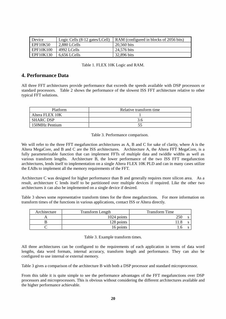
Device Logic Cells (8-12 gates/LCell) RAM (configured in blocks of 2056 bits) EPF10K50 2,880 LCells 20,560 bits EPF10K100 4992 LCells 24,576 bits EPF10K130 6,656 LCells 32,896 bits
Table 1. FLEX 10K Logic and RAM.
4. Performance Data All three FFT architectures provide performance that exceeds the speeds available with DSP processors or standard processors. Table 2 shows the performance of the slowest ISS FFT architecture relative to other typical FFT solutions.
Platform Relative transform time
Altera FLEX 10K 1 SHARC DSP 3.6 150MHz Pentium 55
Table 3. Performance comparison.
We will refer to the three FFT megafunction architectures as A, B and C for sake of clarity, where A is the Altera MegaCore, and B and C are the ISS architectures. Architecture A, the Altera FFT MegaCore, is a fully parameterizable function that can implement FFTs of multiple data and twiddle widths as well as various transform lengths. Architecture B, the lower performance of the two ISS FFT megafunction architectures, lends itself to implementation on a single Altera FLEX 10K PLD and can in many cases utilize the EABs to implement all the memory requirements of the FFT. Architecture C was designed for higher performance than B and generally requires more silicon area. As a result, architecture C lends itself to be partitioned over multiple devices if required. Like the other two architectures it can also be implemented on a single device if desired. Table 3 shows some representative transform times for the three megafunctions. For more information on transform times of the functions in various applications, contact ISS or Altera directly.
Architecture Transform Length Transform Time
A 1024 points 250 s B 128 points 11.8 s C 16 points 1.6 s
Table 3. Example transform times.
All three architectures can be configured to the requirements of each application in terms of data word lengths, data word formats, internal accuracy, transform length and performance. They can also be configured to use internal or external memory. Table 3 gives a comparison of the architecture B with both a DSP processor and standard microprocessor. From this table it is quite simple to see the performance advantages of the FFT megafunctions over DSP processors and microprocessors. This is obvious without considering the different architectures available and the higher performance achievable.
21
5. Discussion The three FFT megafunction architectures are shown to cover a wide range of performance requirements when implemented on Altera FLEX 10K PLDs. The ability to make trade-offs between performance and area for such fundamental DSP functions has never before been available to DSP designers without opting for ASIC solutions. The advantages of these megafunctions to DSP system designers are added to by the manner in which they are constructed and in which they are delivered. Besides the ability of ISS and Altera to provide designers with FFT megafunctions optimized for their particular requirements, they are also configured to minimize the interfacing requirements and to blend in as seamlessly as possible into the particular design. The designer can therefore state his exact requirements and the megafunction can then be delivered as a ‘black box’ solution. The black box solution enables the designer to drop the megafunction into his system without the need to understand its internal operation. With external interfaces minimized, the design process is simplified and shortened. Delivery of the megafunctions also includes a substantial set of supporting material. With constraints files, test bench, graphical symbol file, documentation and technical support provided with each megafunction, the process of designing and testing is further simplified and shortened. The simplification and shortening of the design cycle produces a reduction in development cost and time-to-market, enabling companies to get their products to market ahead of the competition and at a lower cost. The simplification of the design process through the use of megafunctions, as explained earlier, has the added advantage of reducing interface problems and therefore reducing the amount of interface logic required in a design. Added to the fact that many functions can be incorporated into a single PLD in the system, the component count reduces further, reducing the complexity of the circuit board and enabling further savings in product costs. All of these benefits add to the capability of megafunction users to get to market ahead of their competitors and to price their products competitively. For small companies whose main competitive edge is to provide something that its competitors do not, the use of customized megafunctions provides that edge. By being able to specify the exact functionality of each megafunction, companies can add functionality and performance advantages to their products without an increase in component count. These functionality and performance advantages are further emphasized when designers consider the use of off-the-shelf components. When using the same off-the-shelf components which are available to their competitor, it becomes increasingly difficult to establish any competitive advantage with each new design.

22
Conclusions Following on from the discussion above, we can draw on the main points discussed to arrive at a list of the main advantages which the FFT megafunctions produce for DSP designers.
• very high performance • performance/area optimization • reduced development costs • competitive advantage • lower product pricing • faster time-to-market
Other considerations can be made are in terms of the Altera FLEX 10K family itself. With product pricing reducing at a rapid rate and with device gate count increasing, it is becoming more and more attractive to port DSP functionality to these devices to reduce product costs.
23
IV. The Library of Parameterized Modules (LPM)
Craig Lytle Senior Director of Product Planning and Applications
Martin S. Won
Member of Technical Staff
Altera Corporation, 2610 Orchard Parkway San Jose, CA, USA
Introduction Digital logic designers face a difficult task. They must create designs consisting of tens-of-thousands of gates while meeting ever increasing pressure to shorten time-to-market. In addition, designers need to maintain technology independence, without sacrificing silicon efficiency. Meeting these requirements with today’s EDA technology is not easy. Schematic-based design entry, though providing superior efficiency, deals with low level functions that are technology dependent. High-level Design Languages (HDLs) offer technology independence, but not without a significant loss of silicon efficiency and performance. Bridging this gap between technology-independence and efficiency was difficult because there has never been a standard set of functions that were supported by all EDA and IC vendors. This has now changed with the introduction of EDA tools that support the Library of Parameterized Modules (LPM). 1. The History of LPM The LPM standard was proposed in 1990 as a means to enable efficient mapping of digital designs into divergent technologies such as PLDs, Gate Arrays, and Standard Cells. Preliminary versions of the standard appeared in 1991 and again in 1992. The standard was accepted as an Electronic Industries Association (EIA) Interim standard in April 1993 as an adjunct standard to the Electronic Design Interface Format (EDIF). EDIF is the preferred method for transferring designs between the tools of different EDA vendors and from the EDA tools to the Integrated Circuit (IC) vendors. EDIF describes the syntax that represents a logical netlist, and LPM adds a set of functions that describe the logical operation of the netlist. Before LPM, each EDIF netlist would typically contain technology-specific logic functions, making technology-independent design impossible. Although LPM is an adjunct standard to EDIF, it is compatible with any text or graphic design entry tool. In particular, LPM is a welcome addition to Verilog HDL or VHDL designs. LPM is supported by every major EDA tool vendor including Cadence, Mentor Graphics, Viewlogic, and Intergraph. Altera has supported the standard since 1993, and many other PLD companies will support LPM by the end of 1995.

24
2. The Objective of LPM The primary objective of LPM is to enable technology-independent design, without sacrificing efficiency. By using LPM, the designer is freed from deciding the target technology until late in the design flow. All design entry and simulation tools remain technology-independent and rely on the synthesis or fitting tools to efficiently map the design to various technologies. Efficiency is guaranteed because the technology mapping is handled by the technology vendors either during logic synthesis or fitting. To be effective, LPM had to meet the following key criteria: 2.1 Allow Technology-Independent Design Entry The primary goal of LPM was to enable technology-independent design. Designers can work with the LPM modules during design entry and verification without specifying the target technology. 2.2 Allow Efficient Design Mapping Technology-independent design typically means inefficient design. LPM allows designers to use technology-independent design without sacrificing efficiency. The technology mapping of LPM modules is specified by the technology-vendor, so that the most optimum solutions are guaranteed. 2.3 Allow Tool-Independent Design Entry Designers require the ability to migrate a design from one EDA vendor’s tool to another. Many designers, for example, use one vendor for logic synthesis and another vendor for logic simulation. LPM enables designers to migrate designs between EDA vendors while maintaining a high-level logic description of the functions. 2.4 Allow specification of a complete design The LPM set of modules can completely specify the digital logic for any design. Any function that is not included in the initial set of modules, can be created out of the modules. 3. The LPM Functions LPM presently contains 25 different modules, as shown in Figure 1. The small size of the LPM library belies its power. Each of the modules contain parameters that allow the module to expand in many dimensions. For example, the LPM_COUNT module allows the user to specify the width of the counter to be any number from 1-bit to infinity. Figure 1. Current list of LPM Modules. CONST DECODE COUNTER RAM_DQ INPAD INV MUX LATCH RAM_IO OUTPAD AND CLSHIFT DFF ROM BIPAD OR ADD_SUB TFF TTABLE XOR MULTIPLIER FSM BUSTRI ABS In addition to width, the user can specify the features and functionality of the counter. For example, parameters indicate whether the counter counts up or down, or loads synchronously or asynchronously.
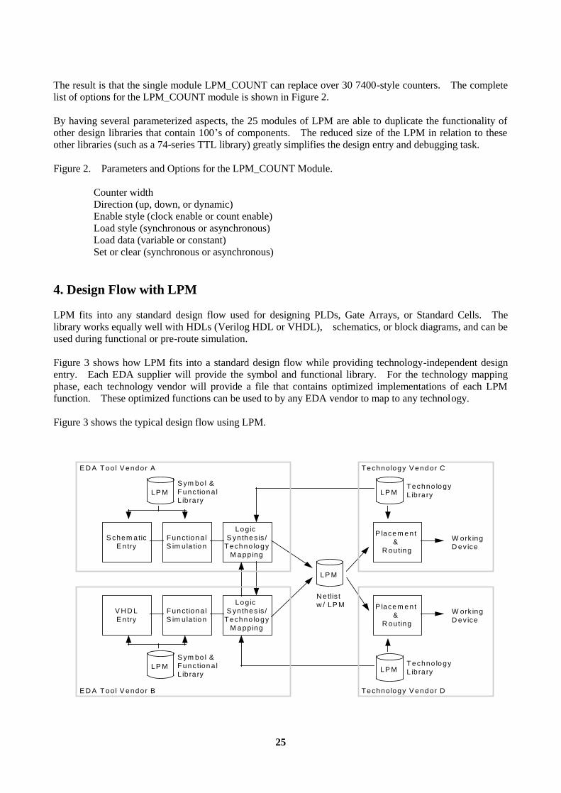
25
The result is that the single module LPM_COUNT can replace over 30 7400-style counters. The complete list of options for the LPM_COUNT module is shown in Figure 2. By having several parameterized aspects, the 25 modules of LPM are able to duplicate the functionality of other design libraries that contain 100’s of components. The reduced size of the LPM in relation to these other libraries (such as a 74-series TTL library) greatly simplifies the design entry and debugging task. Figure 2. Parameters and Options for the LPM_COUNT Module. Counter width Direction (up, down, or dynamic) Enable style (clock enable or count enable) Load style (synchronous or asynchronous) Load data (variable or constant) Set or clear (synchronous or asynchronous) 4. Design Flow with LPM LPM fits into any standard design flow used for designing PLDs, Gate Arrays, or Standard Cells. The library works equally well with HDLs (Verilog HDL or VHDL), schematics, or block diagrams, and can be used during functional or pre-route simulation. Figure 3 shows how LPM fits into a standard design flow while providing technology-independent design entry. Each EDA supplier will provide the symbol and functional library. For the technology mapping phase, each technology vendor will provide a file that contains optimized implementations of each LPM function. These optimized functions can be used to by any EDA vendor to map to any technology. Figure 3 shows the typical design flow using LPM.
S chem aticE n try
Function alS im ula tio n
Lo gic S ynthe s is /
Techno lo gyM a pp ing
S ym bo l & F unc tion a lL ib ra ry
P lacem e nt &
R ou ting
Techno lo gyL ib ra ry
W ork ingD ev ice
V H D LE ntry
Function alS im ula tio n
Lo gic S ynthe s is /
Techno lo gyM a pp ing
P lacem e nt &
R ou ting
W ork ingD ev ice
S ym bo l & F unc tion a lL ib ra ry
Techno lo gyL ib ra ry
E D A T ool V endor A
E D A T ool V endor B
Techno logy V end or C
Techno logy V end or D
LP M
LP M
LP M
LP M
N etlis tw / LP M
LP M
26
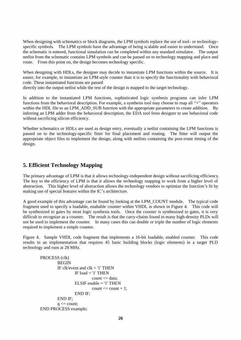
When designing with schematics or block diagrams, the LPM symbols replace the use of tool- or technology-specific symbols. The LPM symbols have the advantage of being scalable and easier to understand. Once the schematic is entered, functional simulation can be completed within any standard simulator. The output netlist from the schematic contains LPM symbols and can be passed on to technology mapping and place and route. From this point on, the design becomes technology specific. When designing with HDLs, the designer may decide to instantiate LPM functions within the source. It is easier, for example, to instantiate an LPM-style counter than it is to specify the functionality with behavioral code. These instantiated functions are passed directly into the output netlist while the rest of the design is mapped to the target technology. In addition to the instantiated LPM functions, sophisticated logic synthesis programs can infer LPM functions from the behavioral description. For example, a synthesis tool may choose to map all “+” operators within the HDL file to an LPM_ADD_SUB function with the appropriate parameters to create addition. By inferring an LPM adder from the behavioral description, the EDA tool frees designer to use behavioral code without sacrificing silicon efficiency. Whether schematics or HDLs are used as design entry, eventually a netlist containing the LPM functions is passed on to the technology-specific fitter for final placement and routing. The fitter will output the appropriate object files to implement the design, along with netlists containing the post-route timing of the design. 5. Efficient Technology Mapping The primary advantage of LPM is that it allows technology-independent design without sacrificing efficiency. The key to the efficiency of LPM is that it allows the technology mapping to work from a higher level of abstraction. This higher level of abstraction allows the technology vendors to optimize the function’s fit by making use of special features within the IC’s architecture. A good example of this advantage can be found by looking at the LPM_COUNT module. The typical code fragment used to specify a loadable, enabable counter within VHDL is shown in Figure 4. This code will be synthesized to gates by most logic synthesis tools. Once the counter is synthesized to gates, it is very difficult to recognize as a counter. The result is that the carry-chains found in many high-density PLDs will not be used to implement the counter. In many cases this can double or triple the number of logic elements required to implement a simple counter. Figure 4. Sample VHDL code fragment that implements a 16-bit loadable, enabled counter. This code results in an implementation that requires 45 basic building blocks (logic elements) in a target PLD technology and runs at 28 MHz. PROCESS (clk) BEGIN IF clk'event and clk = '1' THEN IF load = '1' THEN count <= data; ELSIF enable = '1' THEN count <= count + 1; END IF; END IF; q <= count; END PROCESS example;
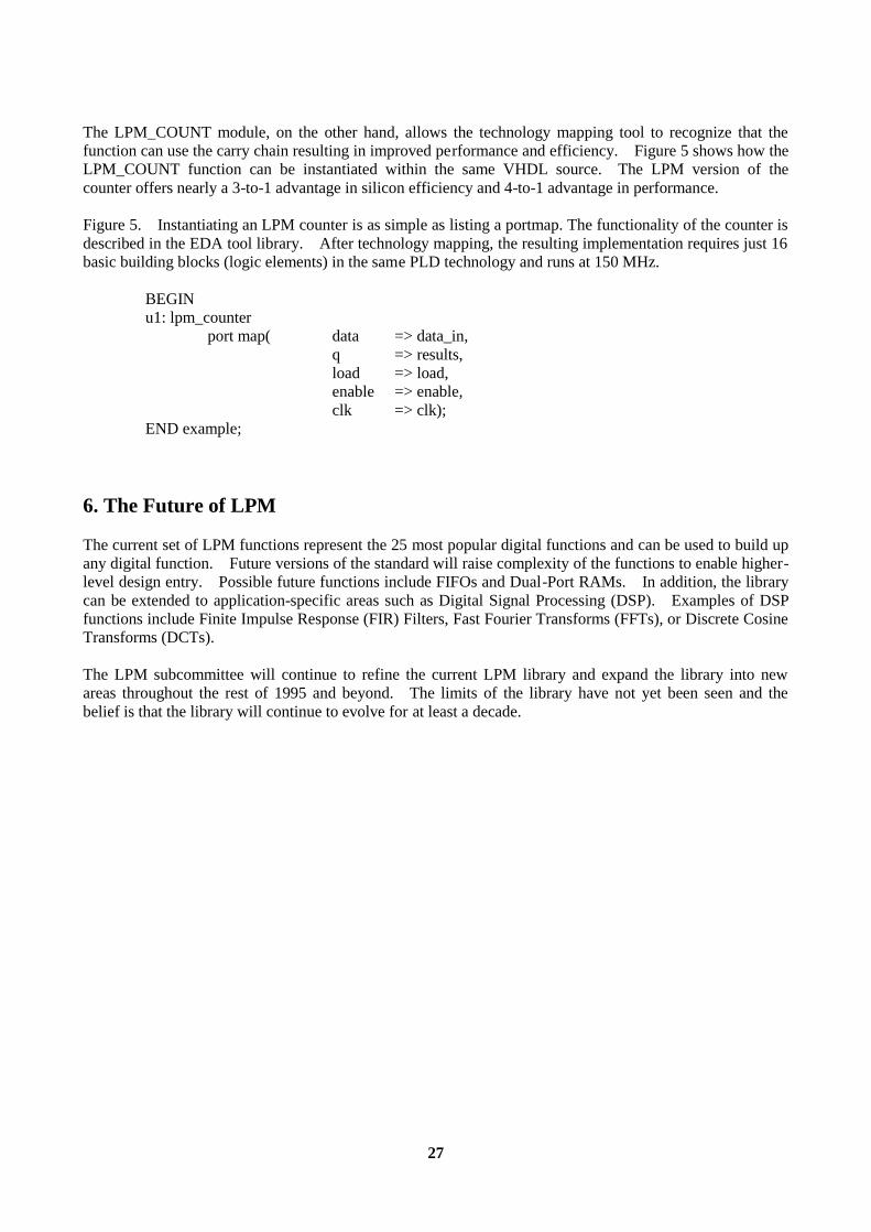
27
The LPM_COUNT module, on the other hand, allows the technology mapping tool to recognize that the function can use the carry chain resulting in improved performance and efficiency. Figure 5 shows how the LPM_COUNT function can be instantiated within the same VHDL source. The LPM version of the counter offers nearly a 3-to-1 advantage in silicon efficiency and 4-to-1 advantage in performance. Figure 5. Instantiating an LPM counter is as simple as listing a portmap. The functionality of the counter is described in the EDA tool library. After technology mapping, the resulting implementation requires just 16 basic building blocks (logic elements) in the same PLD technology and runs at 150 MHz. BEGIN u1: lpm_counter port map( data => data_in, q => results, load => load, enable => enable, clk => clk); END example; 6. The Future of LPM The current set of LPM functions represent the 25 most popular digital functions and can be used to build up any digital function. Future versions of the standard will raise complexity of the functions to enable higher-level design entry. Possible future functions include FIFOs and Dual-Port RAMs. In addition, the library can be extended to application-specific areas such as Digital Signal Processing (DSP). Examples of DSP functions include Finite Impulse Response (FIR) Filters, Fast Fourier Transforms (FFTs), or Discrete Cosine Transforms (DCTs). The LPM subcommittee will continue to refine the current LPM library and expand the library into new areas throughout the rest of 1995 and beyond. The limits of the library have not yet been seen and the belief is that the library will continue to evolve for at least a decade.

28
Conclusion The Library of Parameterized Modules offers designers a means to achieve technology-independent design entry without sacrificing efficiency. The library can be used with schematic, Verilog, or VHDL design entry and is supported by most major EDA vendors. As the LPM expands in scope and support, it will become the standard method of design entry and synthesis over the next five to 20 years. Figure 1. Current list of LPM Modules. CONST DECODE COUNTER RAM_DQ INPAD INV MUX LATCH RAM_IO OUTPAD AND CLSHIFT DFF ROM BIPAD OR ADD_SUB TFF TTABLE XOR MULTIPLIER FSM BUSTRI ABS Figure 2. Parameters and Options for the LPM_COUNT Module. Counter width Direction (up, down, or dynamic) Enable style (clock enable or count enable) Load style (synchronous or asynchronous) Load data (variable or constant) Set or clear (synchronous or asynchronous) Figure 3 shows the typical design flow using LPM.
Schem aticE ntry
FunctionalS im ulation
Logic Synthesis/
Techno logyM apping
Sym bol & FunctionalLibrary
P lacem ent &
Routing
TechnologyLibrary
W orkingDevice
V H DLE ntry
FunctionalS im ulation
Logic Synthesis/
Techno logyM apping
P lacem ent &
Routing
W orkingDevice
Sym bol & FunctionalLibrary
TechnologyLibrary
EDA Tool Vendor A
EDA Tool Vendor B
Technology Vendor C
Technology Vendor D
LP M
LP M
LPM
LPM
Netlistw / LPM
LPM

29
Figure 4. Sample VHDL code fragment that implements a 16-bit loadable, enabled counter. This code results in an implementation that requires 45 basic building blocks (logic elements) in a target PLD technology and runs at 28 MHz. PROCESS (clk) BEGIN IF clk'event and clk = '1' THEN IF load = '1' THEN count <= data; ELSIF enable = '1' THEN count <= count + 1; END IF; END IF; q <= count; END PROCESS example; Figure 5. Instantiating an LPM counter is as simple as listing a portmap. The functionality of the counter is described in the EDA tool library. After technology mapping, the resulting implementation requires just 16 basic building blocks (logic elements) in the same PLD technology and runs at 150 MHz. BEGIN u1: lpm_counter port map( data => data_in, q => results, load => load, enable => enable, clk => clk); END example;
30
V. A Programmable Logic Design Approach to Implementing PCI
Interfaces
Martin Won Senior Applications Engineer
Altera Corporation This paper will discuss a programmable logic approach to implementing Peripheral Component Interconnect (PCI) bus interfaces. PCI is rapidly gaining popularity for its high performance and wide bandwidth, and in order to take full advantage of its capabilities, system designers must consider a number of possible implementations. The portion of the PCI bus scheme that this paper will address is the the interface between the PCI bus itself and any back-end function that needs to use the bus, either to send or receive data. A programmable logic implementation of a PCI interface offers several options that non-programmble logic implementations (i.e. chip sets) do not. The most attractive aspect of using programmable logic for PCI bus interfacing is the flexibility of the implementation. Programmable logic provides the flexibility to customize the interface to the back-end function. There is also the capability to easily change or alter the interface design to update or add features to the overall product. Also, programmable logic features the option to incorporate portions of the back-end function into the programmable logic device itself (if resources are available; see the Hardware Implementation section of this paper), thus conserving board real estate. Finally, another reason for choosing programmable logic over a less-flexible solution is that a dedicated solution might not support all the possible bus cycles specified in the PCI specification, whereas programmable logic is open to support all the existing bus cycles, plus any that may be defined in the future. 1. Customizable Functionality There are a number of areas in a PCI interface that need to be tailored to suit the needs of the function that is being interfaced to a PCI bus. This tailoring ranges in complexity from choosing not to implement certain functions (i.e. parity check and/or parity error) to fine-tuning the logic to meet critical needs (i.e. limiting the response of the control state machine to certain bus cycles to optimize the timing). These and other types of changes are easily made in a programmable logic design approach with straightforward modifications of the design description. Specific modifications will be discussed in the section of this paper titled Modifying/Customizing the Macrofunctions. 2. Description of PCI Macrofunctions A set of PCI interface designs has been created for use with Altera’s programmable logic devices. These designs (or macrofunctions in Altera’s terminology) are meant to serve as the foundations for a PCI interface design, with the designer changing aspects of the macrofunction and adding/removing components to suit the individual needs of the product. At present, there are three macrofunctions: a master interface, a target interface, and a parity generator. A macrofunction for a combined master/target interface is in development. Several Altera devices are specified by the PCI Special Interest Group (SIG) as being PCI-compliant, including many members of the MAX 7000 and FLEX 8000 families. A complete list of these devices is available both from the PCI SIG and from the Altera Marketing department at (408) 894-7000. There is also a complete checklist of items that are associated with PCI compliance; for more information on specificities of Altera’s device compliance, consult Altera’s Application Brief 140: PCI Compliance of Altera Devices.
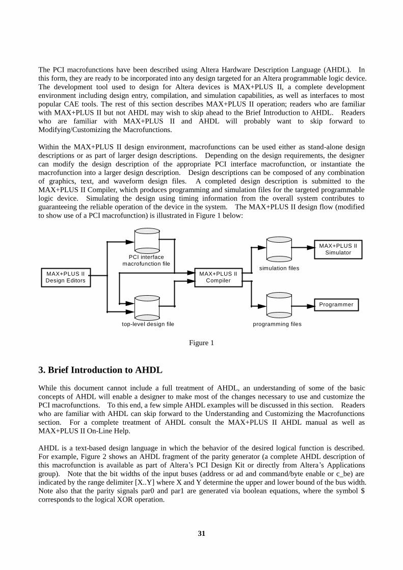
31
The PCI macrofunctions have been described using Altera Hardware Description Language (AHDL). In this form, they are ready to be incorporated into any design targeted for an Altera programmable logic device. The development tool used to design for Altera devices is MAX+PLUS II, a complete development environment including design entry, compilation, and simulation capabilities, as well as interfaces to most popular CAE tools. The rest of this section describes MAX+PLUS II operation; readers who are familiar with MAX+PLUS II but not AHDL may wish to skip ahead to the Brief Introduction to AHDL. Readers who are familiar with MAX+PLUS II and AHDL will probably want to skip forward to Modifying/Customizing the Macrofunctions. Within the MAX+PLUS II design environment, macrofunctions can be used either as stand-alone design descriptions or as part of larger design descriptions. Depending on the design requirements, the designer can modify the design description of the appropriate PCI interface macrofunction, or instantiate the macrofunction into a larger design description. Design descriptions can be composed of any combination of graphics, text, and waveform design files. A completed design description is submitted to the MAX+PLUS II Compiler, which produces programming and simulation files for the targeted programmable logic device. Simulating the design using timing information from the overall system contributes to guaranteeing the reliable operation of the device in the system. The MAX+PLUS II design flow (modified to show use of a PCI macrofunction) is illustrated in Figure 1 below:
PCI interfacemacrofunction file
MAX+PLUS IICompiler
MAX+PLUS IIDesign Editors
top-level design file
MAX+PLUS IISimulator
simulation files
programming files
Programmer
Figure 1 3. Brief Introduction to AHDL While this document cannot include a full treatment of AHDL, an understanding of some of the basic concepts of AHDL will enable a designer to make most of the changes necessary to use and customize the PCI macrofunctions. To this end, a few simple AHDL examples will be discussed in this section. Readers who are familiar with AHDL can skip forward to the Understanding and Customizing the Macrofunctions section. For a complete treatment of AHDL consult the MAX+PLUS II AHDL manual as well as MAX+PLUS II On-Line Help. AHDL is a text-based design language in which the behavior of the desired logical function is described. For example, Figure 2 shows an AHDL fragment of the parity generator (a complete AHDL description of this macrofunction is available as part of Altera’s PCI Design Kit or directly from Altera’s Applications group). Note that the bit widths of the input buses (address or ad and command/byte enable or c_be) are indicated by the range delimiter [X..Y] where X and Y determine the upper and lower bound of the bus width. Note also that the parity signals par0 and par1 are generated via boolean equations, where the symbol $ corresponds to the logical XOR operation.

32
SUBDESIGN pci_par ( ad[31..0], c_be[3..0] : INPUT; parity : OUTPUT; ) VARIABLE par[10..0] : NODE; BEGIN -- Parity generation equations par0 = ad0 $ ad1 $ ad2 $ ad3; par1 = ad4 $ ad5 $ ad6 $ ad7;
The AHDL fragment in Figure 3 below illustrates the declaration of the Base Addess Registers (BAR): SUBDESIGN target ( -- PCI Interface Signals CLK : INPUT; -- PCI Clock AD[31..0] : BIDIR; -- Multiplexed address/data RST : INPUT; -- PCI Master Reset VARIABLE BAR[31..5] : DFF; -- Base Address Registers BEGIN BAR[].clk = CLK; BAR[].clrn = RST; BAR[31..5].d = Write_BAR & AD[31..5] # !Write_BAR & BAR[31..5].q; The AHDL fragment in figure 3 also illustrates the description of the logic required to write a value into the Base Address Registers. The last line of AHDL in the fragment (shown below) defines that the 28-bit value to be placed on the d inputs of the BAR is the value on the address lines ( AD[31..5] ) logically ANDed with the binary signal Write_BAR (defined outside of this fragment) OR the value from the q outputs of the BAR anded with the complement of Write_BAR. BAR[31..5].d = Write_BAR & AD[31..5] # !Write_BAR & BAR[31..5].q; The last item of interest in both AHDL fragments is the use of the two sequential dashes to indicate a comment. This notation can also be used to prevent lines of text in an AHDL design description from being compiled into the hardware implementation of the design. For example, if a designer did not wish to include a PCI master rest input signal (listed as RST in figure 4) in the design, he or she could add two dashes to the beginning of that line as indicated in figure 4 below: SUBDESIGN target (
33
-- PCI Interface Signals CLK : INPUT; -- PCI Clock AD[31..0] : BIDIR; -- Multiplexed address/data -- RST : INPUT; -- PCI Master Reset The other means of commenting out a line of AHDL code is with the percent symbol (%). Unlike the sequential dashes, use of a single percent sign indicates the beginning of a comment, while the second percent sign indicates the end of the comment. For example, if a designer wished to comment out the last two lines of the AHDL fragment in Figure 4 using percent signs, the resulting text would look like Figure 5: SUBDESIGN target ( -- PCI Interface Signals CLK : INPUT; -- PCI Clock % AD[31..0] : BIDIR; -- Multiplexed address/data RST : INPUT; -- PCI Master Reset % AHDL designs are saved as files with a .tdf (Text Design File) extension. MAX+PLUS II recognizes files with the .tdf extension as AHDL design files to be compiled or incorporated into designs for Altera programmable logic devices. 4. Modifying/Customizing the Macrofunctions There are a number of ways a designer might customize the PCI macrofunctions to suit the needs of a particular design. This section of the paper will describe a few of them. The whole range of possible variations on a PCI interface design can not, of course, be encapsulated into any single document, but the intention of covering a few examples here is to convey the effort involved in such changes. The customizations that will be discussed are: (1) Adjusting the width of the address and data buses connecting the interface to the back-end function (2) Including/excluding a parity check/parity error function Other customizations that will be discussed (in somewhat less detail) are: (1) Including some or all of the Configuration Space in the PLD (2) Generating signals for the back-end function The means for customization will be modification of the AHDL design files using any standard ASCII text editor. In this paper, the design file referenced will be the design for the target interface for Altera’s product-term based devices. This file is called TAR_MAX.TDF.

34
5. Adjusting the Width of Address/Data Buses The width requirement for the address and data buses connecting the PCI interface and the back-end function vary with the needs of the back-end function. Changing these widths requires three modifications to the AHDL design. 1. The number and names of the device pins corresponding to these buses must be changed to fit the
desired number and names of the signals. 2. The number of registers that hold the address and/or data information must be modified accordingly. 3. The number of tri-state buffers that control the passage of the address and/or data information
to the outside world must be changed to correspond to the new number of address and/or data lines. In the TAR_MAX.TDF file, signals that connect to the outside world (via device pins) are defined in the first part of the Subdesign section. This section is excerpted in Figure 6 below: SUBDESIGN tar_max ( -- PCI Interface Signals CLK : INPUT; -- PCI Clock AD[31..0] : BIDIR; -- Multiplexed address/data C_BE[3..0] : INPUT; -- Command/Byte enable PAR : BIDIR; -- Parity PERR : BIDIR; -- Parity Error SERR : OUTPUT; -- System Error FRAME : INPUT; -- Transfer Frame IRDY : INPUT; -- Initiator Ready TRDY : BIDIR; -- Target Ready DEVSEL : BIDIR; -- Device Select IDSEL : INPUT; -- ID Select RST : INPUT; -- PCI Master Reset STOP : BIDIR; -- Stop Request -- Interface Back-End Device Signals Addr[7..0] : OUTPUT; -- Address From Device Data[31..0] : BIDIR; -- Data To/From Device -- Dpar : INPUT; -- Data Parity From Device BE[3..0] : OUTPUT; -- Configuration Byte Enables Dev_req : INPUT; -- Request From Device Dev_ack : OUTPUT; -- Transfer Complete Ack. Rd_Wr : OUTPUT; -- Read/Write Cnfg : OUTPUT; -- Configuration Cycle T_abort : INPUT; -- Fatal Error has occured Retry : INPUT; -- Target signaled a retry Reset : OUTPUT; -- PCI Reset ) Figure 6 The address and data buses to the back-end function are the two lines (bolded) directly underneath the

35
comment line “Interface Back-End Device Signals”. Note that the keyword OUTPUT after the colon indicates that the “objects” declared by the name Addr[7..0] are output pins. The first step to modifying the width of these buses is to change the number ranges in the brackets following the names of the signals. For example, the address bus (shown as being 8 bits in width) can be modified to be a 4-bit bus by changing the line: Addr[7..0] : OUTPUT; -- Address From Device to Addr[3..0] : OUTPUT; -- Address From Device Likewise, the data bus Data[31..0]can be modified to any width with a similar operation. Note that the data bus signals are defined to be of type BIDIR, indicating that they are bidirectional signals. The second step is to change the number of registers that hold the address and/or data information and before going to the tri -state buffers. The registers for the address information are called Addr_reg. The line of AHDL in the TAR_MAX.TDF file that indicates the number (and name) of the address registers is in the VARIABLE section. The line is below (note that the keyword DFF after the colon indicates that the “objects” declared by the name Addr_reg[31..0] are D-type flipflops): Addr_reg[31..0] : DFF; -- Register the AD[] The line of AHDL responsible for naming and numbering the data signals is a few lines below the address register line: Data_reg[31..0] : DFF; The lines of AHDL that state the number of tri-state buffers associated with the address and data pins are in the same section (Variable). These lines are listed below (note that the keyword TRI after the colon indicates that the “objects” declared by the names AD_tri[31..0] and Data_tri[31..0] are tri-state buffers): AD_tri[31..0] : TRI; Data_tri[31..0] : TRI; Including/Excluding a Parity Check Function The capability to check parity, produce a parity signal and produce a parity error signal exist within the AHDL designs for both the Master and Target Interface. Parity is produced via another macrofunction, called pci_par, which is referenced within the Master and Target interface designs (in Altera terminology, the use of lower-level macrofunctions within higher-level macrofunctions is called “instantiation”). Exclusion of the parity check signal and/or parity error signal involves “commenting out” portions of AHDL code (commenting a line out is generally preferable to outright deletion for reasons of ease for future modification, but deletion is an option as well). The lines of AHDL to be commented out correspond to: (1) The parity and/or parity error pins (2) The registers and node that hold the parity and/or parity error signals and their output enables (3) The logic and connections for the parity and/or parity error signals The declaration of the parity and parity error pins is included in the Subdesign section of the design file. In the MAX_TAR.TDF file, they appear like this:

36
PAR : BIDIR; -- Parity PERR : BIDIR; -- Parity Error After being commented out, these lines would appear like this: % PAR : BIDIR; -- Parity PERR : BIDIR; -- Parity Error % The registers for the parity and parity error signals (and their output enables) are declared in the Variable section. They appear like this: PERR_reg : DFF; PERRoe : DFF; PAR_reg : DFF; PARoe : DFF; Par_flag1 : DFF; Par_flag2 : DFF; Parity : NODE; The above signals can be commented out by placing a percent sign before the first line and a second percent sign after the last. Finally, the logic and connections for the parity and parity error signals appear in the main body of the design file; percent signs can be used to comment them out in the same manner described above. The signals to be commented out are shown below. PCI_parity.(AD[31..0], C_BE[3..0]) = (AD[31..0], C_BE[3..0]); Parity = PCI_parity.(Parity); PAR = TRI(PAR_reg, TRDYoe); PAR_reg.clk = CLK; PAR_reg.clrn = RST; PAR_reg = Read_BAR & Parity # !Read_BAR & PAR_reg; PARoe.clk = CLK; PARoe.clrn = RST; PARoe = ADoe; PERR = TRI(!PERR_reg, PERRoe); PERR_reg.clk = CLK; PERR_reg.clrn = RST; PERR_reg = Par_flag1 & Parity; Par_flag1.clk = CLK; Par_flag1.clrn = RST; Par_flag1 = S_data & !Rd_Wr & !IRDY & !TRDY # Write_BAR & !RD_WR & !IRDY & !TRDY; Par_flag2.clk = CLK;
37
Par_flag2.clrn = RST; Par_flag2 = Par_flag1; PERRoe.clk = CLK; PERRoe.clrn = RST; PERRoe = S_data & !Rd_Wr & !IRDY & !TRDY # Backoff & !Rd_Wr # Turn_ar & !Rd_Wr # Idle & Par_flag2; A designer who wishes to implement the parity check but not the parity error, can comment out only the AHDL code corresponding to the parity error signal, and this will produce the desired result. 6. Other Customizations There are a number of other ways for a designer to modify these macrofunctions. Any number of signals might also be generated for the requirements of the back-end function. Modification of the AHDL code to include the logic equations for these signals is all that is required to implement these signals. Another possible change is to vary the amount of Configuration Space inside the programmable logic device itself. The TAR_MAX.TDF design includes a 27-bit wide register for the BAR. Less registers might be used if the memory requirements did not require the full 27-bit range. A designer might also wish to include more of the Configuration Space inside the programmable logic device, for example the Command or Status Registers. Including more of the Configuration Space inside the programmable logic device is particularly suited to devices that have on-board RAM (such as the FLASHlogic family). 7. Hardware Implementation This section discusses the actual implementation of a PCI interface in a programmable logic device. The example that will be used is the Target interface placed into a MAX 7000 EPM7160E device. By understanding how the Target interface fits into the EPM7160E, designers can get a clearer idea of the capabilties of programmable logic in PCI interface applications. The design file TAR_MAX.TDF was submitted to MAX+PLUS II and compiled, with MAX 7000 as the target family. The design’s major features are listed below; a complete listing of the TAR_MAX.TDF design file is available from a number of sources listed at the end of this paper (1) PCI Target interface with 32-bit address/data connection to PCI bus (2) 8-bit address and 32-bit data bus to back-end function (3) Generates parity and parity error signals (4) Generates system error signal (5) Includes 27-bit Base Address Register MAX+PLUS II placed the design into the smallest possible device in the family that would accommodate the design: an EPM7160E in the 160-pin QFP package. The following excerpt from the report file (produced by MAX+PLUS II during compilation) indicates some of the resource utilization: Total dedicated input pins used: 4 / 4 (100%) Total I/O pins used: 94 / 100 ( 94%) Total logic cells used: 153 / 160 ( 95%)
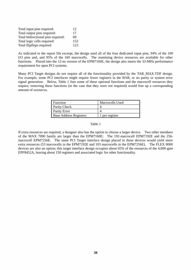
38
Total input pins required: 12 Total output pins required: 17 Total bidirectional pins required: 69 Total logic cells required: 153 Total flipflops required: 123 As indicated in the report file excerpt, the design used all of the four dedicated input pins, 94% of the 100 I/O pins and, and 95% of the 160 macrocells. The reamining device resources are available for other functions. Placed into the 12-ns version of the EPM7160E, the design also meets the 33-MHz performance requirement for open PCI systems. Many PCI Target designs do not require all of the functionality provided by the TAR_MAX.TDF design. For example, some PCI interfaces might require fewer registers in the BAR, or no parity or system error signal generation. Below, Table 1 lists some of these optional functions and the macrocell resources they require; removing these functions (in the case that they were not required) would free up a corresponding amount of resources.
Function Macrocells Used Parity Check 4 Parity Error 4 Base Address Registers 1 per register
Table 1
If extra resources are required, a designer also has the option to choose a larger device. Two other members of the MAX 7000 family are larger than the EPM7160E: The 192-macrocell EPM7192E and the 256-macrocell EPM7256E. The same PCI Target interface design placed in these devices would yield more extra resources (53 macrocells in the EPM7192E and 103 macrocells in the EPM7256E). The FLEX 8000 devices are also an option; this target interface design occupies about 65% of the resources of the 4,000-gate EPF8452A, leaving about 150 registers and associated logic for other functionality.
39
Conclusion A programmable logic solution to a PCI interface offers flexibility and options that a dedicated chip set cannot. These options include the ability to customize the interaction with the back-end design, include or exclude functions that may or may not be needed, and include back-end function logic into the programmable logic device to conserve board real estate. Altera’s PCI interface macrofunctions are designed to serve engineers as foundations upon which to build their own PCI interfaces. A number of Altera’s devices are suitable for impementing PCI interface designs in addition to the one discussed in this paper, including several members of the MAX 7000, FLEX 8000, MAX 9000, and FLASHlogic families. Finally, Altera’s Applications group is available at (800) 800-EPLD to assist any engineer in utilizing the macrofunctions to their best potential. Obtaining the Macrofunctions The PCI macrofunctions are available from several sources, including: (1) Altera’s PCI Design Kit (obtainable from Altera Marketing at (408) 894-7000) (2) Altera’s Applications group at (800) 800-EPLD or (408) 894-7000 (3) Altera Applications BBS at (408) 954-0104 in the form of the file PCI_10.EXE (4) Altera’s ftp site: ftp.altera.com
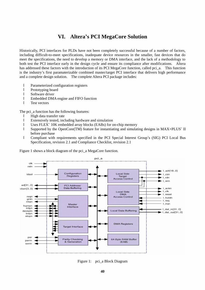
40
VI. Altera’s PCI MegaCore Solution
Historically, PCI interfaces for PLDs have not been completely successful because of a number of factors, including difficult-to-meet specifications, inadequate device resources in the smaller, fast devices that do meet the specifications, the need to develop a memory or DMA interface, and the lack of a methodology to both test the PCI interface early in the design cycle and ensure its compliance after modifications. Altera has addressed these factors with the introduction of its PCI MegaCore function, called pci_a. This function is the industry’s first paramaterizable combined master/target PCI interface that delivers high performance and a complete design solution. The complete Altera PCI package includes: l Parameterized configuration registers l Prototyping board l Software driver l Embedded DMA engine and FIFO function l Test vectors
The pci_a function has the following features: l High data transfer rate l Extensively tested, including hardware and simulation l Uses FLEX¨ 10K embedded array blocks (EABs) for on-chip memory l Supported by the OpenCore(TM) feature for instantiating and simulating designs in MAX+PLUS¨ II
before purchase l Compliant with requirements specified in the PCI Special Interest Group’s (SIG) PCI Local Bus
Specification, revision 2.1 and Compliance Checklist, revision 2.1 Figure 1 shows a block diagram of the pci_a MegaCore function.
Figure 1: pci_a Block Diagram
41
The pci_a MegaCore function contains a DMA control engine that supports burst read and write data transfers. To transfer data on the PCI bus, the system software loads the internal DMA registers. The function is then ready to accept the local DMA request signal that enables the master to initiate data transfers on the bus. For example, in a burst read, the master stores the read information in the RAM buffer from the PCI bus. After the burst transaction is completed, the pci_a MegaCore function indicates to the local side that it will transfer data from the RAM buffer to the local side memory. Similarly, in a burst write, the function indicates to the local side that it is ready to transfer data from the local side to the RAM buffer. When the RAM buffer is full, or the pci_a MegaCore function has the last data word, the function requests access to the PCI bus. After the arbiter grants the function access, the function will transfer all data from the RAM buffer to the PCI bus. In the pci_a MegaCore function, the target capability is used for single data phase accesses. Target accesses are typically used to access configuration registers, internal DMA registers, and external target memory space. The pci_a MegaCore function offers high data bandwidth and zero-wait state burst data transfers. The function can perform a zero-wait state PCI read with a bandwidth of 107 Mbytes/second and a zero-wait state PCI write at 102 Mbytes/second. It also supports a 256-byte, header type-0 configuration. Table 1 shows the key performance characteristics for the pci_a MegaCore function.
Characteristic Values Clock Rate 33 MHz
Read data burst transfer rate 107 Mbytes/second Write data burst transfer rate 102 Mbytes/second
Table 1: Key pci_a Performance Characteristics
The pci_a MegaCore function is optimized for the EPF10K30RC240-3 and EPF10K20RC240-3 devices. Future support is planned for FLEX 10KA devices. The pci_a MegaCore function uses less than 50% of the logic elements (LEs) available in an EPF10K30RC240-3 device. The remaining logic elements (LEs) can be used for user-defined local-side customization. Table 2 shows the typical device utilization for the pci_a MegaCore function in the EPF10K30RC240-3 device with 1,728 LEs available.
Function LEs pci_a MegaCore function (includes complete DMA circuit)
850
Local side with custom logic 878
Table 2: Typical Device Utilization for pci_a A PCI prototyping board is included in Altera’s PCI package for implementing and testing PCI designs. The PCI prototype board contains an EPF10K30RC240-3 device that can be configured with a PCI design, a connector socket for the PCI bus interface, and other sockets for accessing the EPF10K30RC240-3 device I/O pins. The board also has 128 Kbytes of SRAM for the target address space and allows the local-side function to interface with a standard parallel or VGA port. A second-generation PCI MegaCore function will provide the same 33-MHz, zero-wait state performance as well as a decoupled memory subsystem. This new function will give you the flexibility to use the existing DMA controller to minimize design and development effort, or design a custom memory interface to meet specific requirements of your design. Future PCI functions will provide enhanced performance and features.

42
Altera’s OpenCore(TM) feature allows you to “test drive” MegaCore functions like pci_a before you purchase them. With the OpenCore feature, MegaCore functions can be instantiated in your design, and then compiled and simulated using the MAX+PLUS II development system, giving you a preview of exactly how the function will fit into an Altera device. When you are ready to program a device, you must license the MegaCore function. To test-drive the PCI master/target MegaCore function using the OpenCore feature, simply download the function from Altera’s world-wide web site (http://www.altera.com) and try it in your design. For more information about Altera’s PCI solution, refer to the PCI Master/Target MegaCore Function with DMA Data Sheet or contact your local Altera sales representative.

43
VII. A VHDL Design Approach to a Master/Target PCI Interface
Leo K. Wong
Applications Engineer, Altera Corporation
Martin Won Applications Supervisor, Altera Corporation
Subbu Ganesan
Associate Director of Hardware Engineering, ZeitNet, Inc.
ABSTRACT This paper describes a design approach to implementing a Peripheral Component Interconnect (PCI) interface that allows for the maximum amount of design flexibility while achieving an actual working solution in a relatively short amount of time. The approach involves two key elements: VHDL and programmable logic devices. The portability of VHDL and the rapid prototyping time of programmable logic, combined with the flexibility afforded by both creates a design approach that provides the designer the opportunity to make changes to the design while still working towards a final hardware solution. In the experience of the ZeitNet project (an interface for an ATM adapter card), this approach yielded a demonstratable product in four months; in another three months, burst mode was added to the design and final testing was completed, resulting in a finished product in only seven months from product inception. Furthermore, considerations for future development of PCI interface are also included. 1. INTRODUCTION Most engineers are faced with the challenges of ever shorter production cycle, higher performance requirements as well as cost pressure in every project. A well defined design methodology is critical in meeting these goals. Our sample design is a PCI bus ATM adapter card. Table 1 shows the requirements of the project.
High Performance Full PCI and ATM compliance; Zero-wait-state Burst transaction; Sustaining full duplex line speed
Interoperability Product should be accepted by multiple platform for maximum customer appeal.
Vendor Independence Need flexibility to migrate to future silicon technology if desired.
Meet product rollout deadline Three to four month design cycle time limit from concept to silicon.
Table 1 Project objectives
The following sections will discuss these objectives in details and explain how these objectives are met by the proposed methodology.
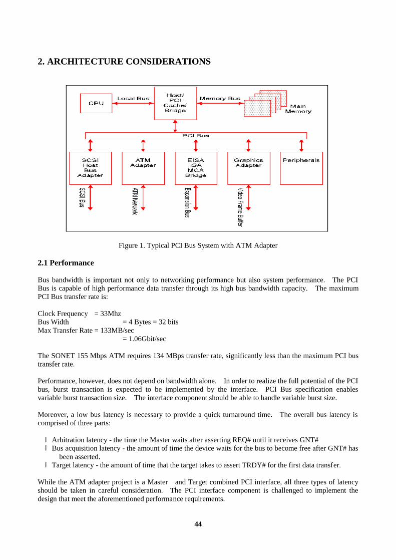
44
2. ARCHITECTURE CONSIDERATIONS
Figure 1. Typical PCI Bus System with ATM Adapter 2.1 Performance Bus bandwidth is important not only to networking performance but also system performance. The PCI Bus is capable of high performance data transfer through its high bus bandwidth capacity. The maximum PCI Bus transfer rate is: Clock Frequency = 33Mhz Bus Width = 4 Bytes = 32 bits Max Transfer Rate = 133MB/sec
= 1.06Gbit/sec The SONET 155 Mbps ATM requires 134 MBps transfer rate, significantly less than the maximum PCI bus transfer rate. Performance, however, does not depend on bandwidth alone. In order to realize the full potential of the PCI bus, burst transaction is expected to be implemented by the interface. PCI Bus specification enables variable burst transaction size. The interface component should be able to handle variable burst size. Moreover, a low bus latency is necessary to provide a quick turnaround time. The overall bus latency is comprised of three parts: l Arbitration latency - the time the Master waits after asserting REQ# until it receives GNT# l Bus acquisition latency - the amount of time the device waits for the bus to become free after GNT# has
been asserted. l Target latency - the amount of time that the target takes to assert TRDY# for the first data transfer.
While the ATM adapter project is a Master and Target combined PCI interface, all three types of latency should be taken in careful consideration. The PCI interface component is challenged to implement the design that meet the aforementioned performance requirements.
45
2.2 Interoperability To ensure the widest possible market acceptance, products should be accepted by as many platforms as possible. As a bus architecture, PCI promises processor independence. However, due to the evolving nature of the PCI architecture, there are systems that does not adhere strictly to the latest standard. It is highly desirable to have a versatile PCI interface component to implement the required modifications in accordance with the operating platform. 2.3 Vendor Independence Depending on the market demand and thus production volume, engineers should have the flexibility to switch from one silicon technology to another. For instance, at mid-to-lower volume production, programmable logic device is ideal for its flexibility, zero NRE cost and low inventory risk. In high volume production, it might be more cost effective to migrate to a Masked Programmable Logic Device (MPLD) or an ASIC solution. An ideal engineering methodology should provide a quick migration path to the most cost effective silicon solution in reaction to market demand. Proven transition path from one silicon technology to another should be provided. 2.4 Design cycle The ATM adapter project was under tremendous time pressure. The month was March, and ZeitNet was scheduled to demonstrate their ATM adapter card at the Tokyo Interop show in July. There were fourteen weeks available from product definition to silicon realization.
3. System Methodology To achieve the project’s challenging goals: fully PCI and ATM compliant, low cost and flexibility within three-to-four months, designers must weigh several inter-depending aspects of their engineering cycles. Critical to a project’s success are the design entry method, EDA tools and the silicon choice. 3.1 Hardware Selection At the time, to implement a PCI interface for the ATM card, there are mainly two selection: PCI chipsets or programmable logic device. Off-the-shelf PCI interface ASIC or PCI chipsets decrease the resources required for in-house development, but the ones available on the market lacked the flexibility for customization. Due to this shortcoming, the chipsets were deemed inappropriate for the project.
3.2 Design Entry An industry standard high-level hardware description language is desirable to ensure smooth future migration in technology. VHDL satisfied the need because of its wide acceptance in the EDA community. While designers usually need to instantiate device specific primitive for optimal performance and area results, careful modularization can lead to high degree of design re-use in future silicon technology. By modularizing design, designers separate the universal behavioral code from the device specific primitives instantiation. The behavioral core, written in VHDL, can be re-used in other synthesis tools when porting
46
to other silicon technologies. While the primitive instantiations maintain close and effective control over the interface component. 3.3 PLD Selection The next decision was to choose a programmable logic device that could implement a combined master/target PCI interface within a reasonable amount of time. Among the range of PCI-compliant devices offered by programmable logic vendors, FLASHlogic devices and MAX 7000E devices from Altera, and XC7000 EPLDs from Xilinx were explored. The first concern for a programmable logic implementation was fitting the entire combined master/target interface into a single device. The FlashLogic devices were examined and their logic capacity is deemed insufficient to fit all functionalities into the largest member of that family, although it did offer several features that were attractive for PCI interface design, including very predictable timing, on-board RAM, and open-drain outputs. The same resource limitations seemed to hold true for the XC7000 devices from Xilinx, in addition to suspicions that the critical timing required for the PCI interface would be difficult to achieve in those devices. The final potential set of devices proved to be the ideal choice: MAX 7000E. By estimation, the largest devices from the family would accommodate a combined master/target design.
3.3 EDA tool selection Traditionally, there has always been tradeoff between design abstraction and efficient silicon control. On one hand, using a proprietary semiconductor vendor tool provide efficient design and synthesis support for the specific component, but it is usually difficult to port the design to other technologies. On the other hand, by choosing a standard EDA design platform, designers risk sacrificing the tight integration, but gain the ease of migration to various ASIC or gate array technologies. The development tools chosen for this ATM project is MAX+PLUS II, which includes a VHDL compiler. The tool can directly accept VHDL text entry, synthesize, place & route, simulate and generating programming file for MAX 7000E device without the burden of third-party tool translation. This design flow provides tight integration, allowing quick design changes and iterations. Moreover, MAX+PLUS II offers proven migration path interfacing with major third party EDA tools through EDIF netlists and vendor libraries. To simulate the design on a board level, tools from Model Technology was employed. The process of developing the VHDL code required for the design took about 2 weeks; simulation was completed one month later. 4. IMPLEMENTATION 4.1 Implementing Functionality In order to shorten the design cycle, VHDL design code was developed in parallel with the device selection process; the goal was to work towards creating a functionally correct VHDL design using a VHDL simulator, and by the time of its completion, place the design into a device.
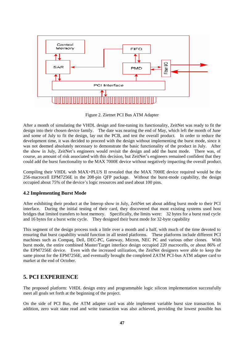
47
Figure 2. Zietnet PCI Bus ATM Adapter After a month of simulating the VHDL design and fine-tuning its functionality, ZeitNet was ready to fit the design into their chosen device family. The date was nearing the end of May, which left the month of June and some of July to fit the design, lay out the PCB, and test the overall product. In order to reduce the development time, it was decided to proceed with the design without implementing the burst mode, since it was not deemed absolutely necessary to demonstrate the basic functionality of the product in July. After the show in July, ZeitNet’s engineers would revisit the design and add the burst mode. There was, of course, an amount of risk associated with this decision, but ZeitNet’s engineers remained confident that they could add the burst functionality to the MAX 7000E device without negatively impacting the overall product. Compiling their VHDL with MAX+PLUS II revealed that the MAX 7000E device required would be the 256-macrocell EPM7256E in the 208-pin QFP package. Without the burst-mode capability, the design occupied about 75% of the device’s logic resources and used about 100 pins. 4.2 Implementing Burst Mode After exhibiting their product at the Interop show in July, ZeitNet set about adding burst mode to their PCI interface. During the initial testing of their card, they discovered that most existing systems used host bridges that limited transfers to host memory. Specifically, the limits were: 32 bytes for a burst read cycle and 16 bytes for a burst write cycle. They designed their burst mode for 32-byte capability This segment of the design process took a little over a month and a half, with much of the time devoted to ensuring that burst capability would function in all tested platforms. These platforms include different PCI machines such as Compaq, Dell, DEC-PC, Gateway, Micron, NEC PC and various other clones. With burst mode, the entire combined Master/Target interface design occupied 220 macrocells, or about 86% of the EPM7256E device. Even with the increased utilization, the ZeitNet designers were able to keep the same pinout for the EPM7256E, and eventually brought the completed ZATM PCI-bus ATM adapter card to market at the end of October. 5. PCI EXPERIENCE The proposed platform: VHDL design entry and programmable logic silicon implementation successfully meet all goals set forth at the beginning of the project. On the side of PCI Bus, the ATM adapter card was able implement variable burst size transaction. In addition, zero wait state read and write transaction was also achieved, providing the lowest possible bus

48
latency. These abilities actualize the full performance potential of the PCI bus. On the backend ATM network, full duplex line speed was sustained. In terms of migration ease, with the help of the tool, designers estimate that they would able to re-use 80-90% of their VHDL code to port their design to an ASIC in the future. The versatility of the proposed platform was proven as the same design was re-target for another programmable logic device, an EPF8820A, a member of the FLEX 8000 PLD family, later in the production cycle.2 More importantly, Zeitnet was able to achieve all goals within the specified time frame: the product meet the trade show demonstration as well as the production deadline. 6. FUTURE ROADMAP Looking forward, there are several paths of modifications, mostly related to the evolving nature of the PCI standard and systems offering PCI compatibility. 1. As noted earlier, the host bridges in most of the tested systems limited transfers to the host memory.
The adapter card was designed accordingly, but future host bridges is expected to provide larger transfers in the future.
2. None of the tested system had implemented the latency timer. Correspondingly, no latency timer was implemented in the adapter card. This functionality is expected to be added when latency is supported by more systems.
These are functionality concerns for the future of PCI as an evolving architecture. Meanwhile, the interface component should be versatile enough to handle these modifications.
2 While MAX 7000E is a AND-OR gates-based CPLD built on E2PROM technology, FLEX 8000 is a Look-Up Table based SRAM technology.

49
Conclusion From this case study, one can conclude that all engineering challenges were met. While the final product not only meet release schedule, it also attain high performance and maintain a versatile future growth path. It is obvious that the benefits of the proposed methodology can readily be extended to other areas of electronic engineering. Flexible engineering control such as shortened time-to-market, versatile volume adjustment, and vendor independence; high performance silicon technologies coupled with easy to use software are universal advantages all designers should utilize. Author biographies Leo Wong is an applications engineer with Altera Corporation (San Jose, CA), where he is involved in PCI design implementation, megafunction partners liaison, and programmable logic applications consultation. Leo holds degree in Electrical Engineering and Computer Science from University of California at Berkeley. Martin Won is the Applications supervisor of Technical Communications for Altera Corporation, where he has worked for 5 years. His responsibilities include writing and publishing articles, creating and presenting Altera's technical seminars, and producing Altera's quarterly newsletter for its customers. Mr. Won holds a B.S. in Electrical and Computer Engineering from the University of California at Santa Barbara.
50
VIII. Interfacing a PowerPC 403GC to a PCI Bus
David Raaum, Staff Engineer
PLX Technology
David Greenfield, Manager, Development Tools Altera Corporation
Martin S. Won, Member of Technical Staff
Altera Corporation Introduction The PowerPC 403 processors have proved to be successful engines for high-performance embedded systems (switches, routers, printer engines) and I/O adapters (communications, disk control, imaging). The PCI bus, already a well-established standard for PCs and servers, is also appearing in 32-bit embedded systems. This article describes how to interface a PowerPC 403GC CPU to a 33-MHz PCI bus. The interface design includes a PCI-to-host bridge device and a programmable logic device. With this implementation, the PowerPC CPU can perform memory, I/O and configuration cycles upon the PCI bus. Additionally, any master device on the PCI bus may access memory (DRAM) on the local bus. Finally, this implementation allows bursts of up to 16 words in length. PCI provides tremendous bus performance for embedded applications through 33 MHz system performance and 32-bit burst mode capability. However, even after a processor is selected and the PCI interface is chosen, abundant design options remain which impact system performance and time-to-market. This paper addresses the issues of PCI function selection criteria from among standard product, programmable logic and ASIC implementations. The paper also addresses design issues relating to interfacing the PCI bridge device with the embedded processor and memory on the local bus. The paper presents a complete solution to implement the PCI bridge, local bus interface and processor needs. Our approach will be to first look at a PCI overview to understand its advantages. Then, we’ll focus on the specific benefits offered for embedded systems by the PCI bus and the PowerPC 403 processor. Next, we’ll look at a design that interfaces the PowerPC 403 to the PCI bus before concluding with an analysis of its performance considerations. The goal of PCI was to offer an open bus standard that provided high performance by allowing bus masters to directly access the main memory, as well as providing a way for CPUs to directly access the devices connected to the PCI bus. PCI’s growth to higher bandwidth is ensured with an upgrade path from a 32-bit bus to a 64-bit bus. Variable-length read & write bursts as well as scalable bus frequencies (from 16 to 33 MHz) broaden PCI’s appeal. The PCI bus also benefits from lower cost. Similarities between the master and target interface design allow a multiplexed-architecture design to fulfill both functions. Finally, the interface design is optimized for implementation in silicon, allowing for interface costs to decrease in the same manner as any other semiconductor solution produced in volume. Besides better performance, another user benefit of PCI is the automatic configuration of PCI add-in boards and components. PCI’s longevity is also improved by the fact that it is processor independent, has an upgrade path to 64-bit addressing, and that it provides for both 3.3 and 5-volt signaling environments.

51
PCI has additional features in the areas of flexibility and reliability. PCI’s flexibility allows for bus masters to directly access any other master or target device. Additionally, data integrity is maintained with parity for both data and addresses. Although PCI was initially developed for personal computing, the high bandwidth and real-time deterministic response is ideal for data communications and industrial applications. PCI is now a viable option for system implementations that previously considered Multibus and VME options. PCI is also used extensively for intraboard communication within a system as PCI interfaces are now found on ethernet, ATM, and other standard products. However, standard PCI interfaces are often not available for all devices within a system and a PCI interface chip is needed for connection to the bus. The PowerPC offers a number of advantages for embedded systems. First, it is a scalable processor architecture, ranging from the 401GF (in the $10 to $15 range) to the 604, which is at the heart of some of the industry’s most powerful workstations. One of the features that fosters this scalability is a clean-layered technology that enables the adding and deleting of features not applicable to a particular application (i.e., all features related to memory management are clearly delineated and well contained). Also, instructions may execute in any order as long as the results are consistent within ordered execution, which, along with an effort in avoiding instruction interlock, allows easy implementation of superscalar designs with several execution units (the PowerPC 604 has six). Another advantage of the PowerPC architecture is its workstation heritage, which has fostered better tools and cross-platform development environments. PowerPC processors themselves are available from multiple sources (IBM and Motorola), and they enjoy a wide range of support both in terms of development tools and applications (over 100 third parties support PowerPC). There are a couple different ways to build an interface between the PowerPC 403GC, its local bus, and a PCI bus. These approaches include: (1) Designing a custom ASIC from the ground up (2) Designing a custom ASIC with an interface core (3) Using a programmable logic device (4) Using a standard PCI interface component and a programmable logic device (PLD) The first approach, building a custom ASIC, has the advantage of resulting in a low-volume cost, single-chip solution. However, of the available approaches, it is also likely to involve the lengthiest design development time. The second option involves using a pre-existing PCI bridge core and requires a designer to create the rest of the necessary logic. While this option offers the advantage of a shorter development time, that benefit must be balanced with the cost of the bridge core (potentially $30K to $250K). Another solution to consider is to build the interface and bridge completely in a programmable logic device. This solution is similar to the ASIC solution in that designer must create the bridge design, but it is attractive for its shorter development time and likely lower development costs (working prototypes are available, debugged and turned around much more quickly). The last solution to consider is to take advantage of existing PCI bridge components and use programmable logic to implement the remaining required logic. This solution probably has the shortest development time and cost of all the options, but also has the disadvantage of being a two-chip solution. Since it offers the most clear advantages and relatively few disadvantages, it is this option that we pursue in this paper. The functions fulfilled by the components in this solution are as follows: first, the standard PCI bridge connects the local bus (CPU and DRAM in this case) to the PCI bus. The programmable logic device
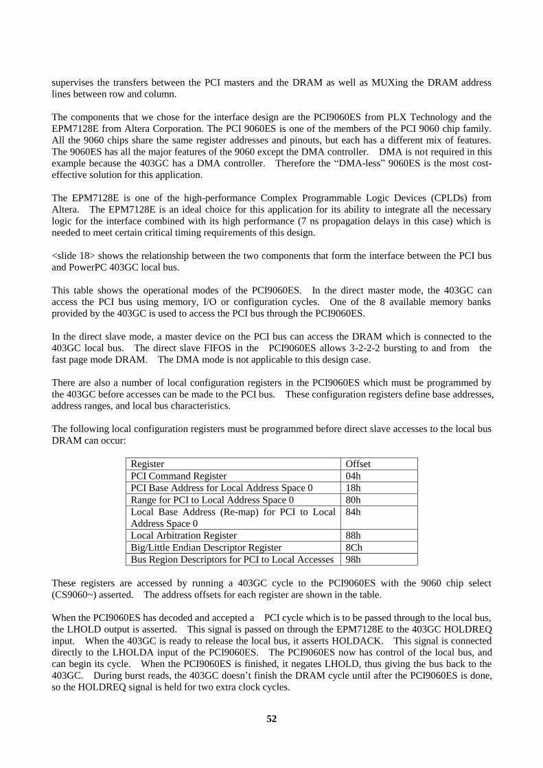
52
supervises the transfers between the PCI masters and the DRAM as well as MUXing the DRAM address lines between row and column. The components that we chose for the interface design are the PCI9060ES from PLX Technology and the EPM7128E from Altera Corporation. The PCI 9060ES is one of the members of the PCI 9060 chip family. All the 9060 chips share the same register addresses and pinouts, but each has a different mix of features. The 9060ES has all the major features of the 9060 except the DMA controller. DMA is not required in this example because the 403GC has a DMA controller. Therefore the “DMA-less” 9060ES is the most cost-effective solution for this application. The EPM7128E is one of the high-performance Complex Programmable Logic Devices (CPLDs) from Altera. The EPM7128E is an ideal choice for this application for its ability to integrate all the necessary logic for the interface combined with its high performance (7 ns propagation delays in this case) which is needed to meet certain critical timing requirements of this design. <slide 18> shows the relationship between the two components that form the interface between the PCI bus and PowerPC 403GC local bus. This table shows the operational modes of the PCI9060ES. In the direct master mode, the 403GC can access the PCI bus using memory, I/O or configuration cycles. One of the 8 available memory banks provided by the 403GC is used to access the PCI bus through the PCI9060ES. In the direct slave mode, a master device on the PCI bus can access the DRAM which is connected to the 403GC local bus. The direct slave FIFOS in the PCI9060ES allows 3-2-2-2 bursting to and from the fast page mode DRAM. The DMA mode is not applicable to this design case. There are also a number of local configuration registers in the PCI9060ES which must be programmed by the 403GC before accesses can be made to the PCI bus. These configuration registers define base addresses, address ranges, and local bus characteristics. The following local configuration registers must be programmed before direct slave accesses to the local bus DRAM can occur:
Register Offset PCI Command Register 04h PCI Base Address for Local Address Space 0 18h Range for PCI to Local Address Space 0 80h Local Base Address (Re-map) for PCI to Local Address Space 0
84h
Local Arbitration Register 88h Big/Little Endian Descriptor Register 8Ch Bus Region Descriptors for PCI to Local Accesses 98h
These registers are accessed by running a 403GC cycle to the PCI9060ES with the 9060 chip select (CS9060~) asserted. The address offsets for each register are shown in the table. When the PCI9060ES has decoded and accepted a PCI cycle which is to be passed through to the local bus, the LHOLD output is asserted. This signal is passed on through the EPM7128E to the 403GC HOLDREQ input. When the 403GC is ready to release the local bus, it asserts HOLDACK. This signal is connected directly to the LHOLDA input of the PCI9060ES. The PCI9060ES now has control of the local bus, and can begin its cycle. When the PCI9060ES is finished, it negates LHOLD, thus giving the bus back to the 403GC. During burst reads, the 403GC doesn’t finish the DRAM cycle until after the PCI9060ES is done, so the HOLDREQ signal is held for two extra clock cycles.
53
The PCI9060ES has both direct master and direct slave transfer capabilities. The direct master mode allows a device (403GC) on the local bus to perform memory, I/O and configuration cycles to the PCI bus. The direct slave mode allows a master device on the PCI bus to access memory (DRAM) on the local bus. The PCI9060ES allows the local bus to operate asynchronously to the PCI bus through the use of bi-directional FIFOs. In this application the PCI bus operates at 33 MHz while the local bus is clocked at 25 MHz. Note that the address and data buses on the 403GC designate bit 0 as the most significant bit. Also, the 403GC does not produce the upper 6 address bits, so its maximum addressing range for one bank is 64 Mbytes. A direct master or configuration write cycle is initiated by the 403GC when it asserts the chip select assigned to the PCI9060 and PCI bus. As with read cycles, it also asserts an address (A6:29), read/write status (PR/W), and byte enables (WBE[0:3]). The PCI state machine in EPM7128E device detects this cycle and transitions to state P0 where the address is strobed into the PCI9060ES using ADS. The byte enables, read/write status, and address are mapped in the same way as read cycles. The READY input to the 403GC is negated, causing it to insert wait states. The PCI9060ES then runs the requested PCI or internal register cycle and asserts RDYO~ when the write has been completed. The state machine jumps to state P2 where READY is asserted to the 403GC. Once READY has been detected, the 403GC will complete the write cycle at the end of the next clock period. The state machine jumps to state P3 during the last clock cycle of the transfer. The state machine then returns to PIDLE and waits for another chip select from the 403GC. A direct master or configuration read cycle is initiated by the 403GC when it asserts the chip select assigned to the PCI9060 and PCI bus. It also asserts an address (A6:29), read/write status (PR/W), and byte enables (WBE[0:3]). The PCI state machine in the EPM7128E device detects this cycle and transitions to state P4 where the address is strobed into the PCI9060ES using ADS. The WBE signals are mapped into the LBE inputs to the PCI9060ES, and the PR/W signal is inverted to become LW/R. Since the 403GC only produces 26 address bits, the upper six address bits to the PCI9060ES are forced to zero. The READY input to the 403GC is negated, causing it to insert wait states. The PCI9060ES has a WAITI~ input pin which allows a master to control the duration of the read data presented by the PCI9060ES. At the beginning of a read cycle, this input is asserted. The PCI9060ES then runs the requested PCI or internal register cycle and asserts RDYO~ when the data is available. The state machine jumps to state P6 where READY is asserted to the 403GC. Once READY has been detected, the data will be sampled by the 403GC at the end of the next clock period. The state machine jumps to state P7 where the WAITI~ signal is negated, allowing the PCI9060ES to complete the read cycle. The 403GC reads the data at the end of this cycle. The state machine returns to PIDLE and waits for another chip select from the 403GC. A direct slave write cycle is initiated by the PCI9060ES when it asserts address strobe (ADS~). It also asserts an address (A[31:2]), write/read status (LW/R), byte enables (LBE[3:0]), and burst last (BLAST~). The DRAMCTL state machine in the EPM7128E device detects this cycle and transitions to state S1 where a DRAM write cycle is initiated. If an unaligned write cycle is detected, then the state machine will go to state S5. More about unaligned transfers later. The XREQ and XSIZ[0:1] inputs to the 403GC are used to initiate a DRAM cycle. The XSIZ inputs are decoded as follows:
54
XSIZ[0:1] Operation 00 Byte Transfer (8 bits) 01 Halfword Transfer (16 bits) 10 Fullword Transfer (32 bits) 11 Burst Fullword Transfer
The byte address is determined by the WBE2(A30) and WBE3(A31) inputs to the 403GC, and is derived from the LBE outputs of the PCI9060ES. After the state machine asserts XREQ~, it checks BLAST~ to determine if this is a single or burst transfer. If it is a single transfer, it waits in state S4 for the 403GC to assert XACK~, indicating that the data has been written. The RDYI~ input to the PCI9060ES is asserted, causing the write cycle to be completed. For a burst cycle, the state machine waits in state S2, where XREQ~ is continuously activated. When BLAST~ is asserted, the PCI9060ES is ready to finish the write burst. The 403GC always writes one extra word after XREQ~ is negated. In this application, the RDYI~ input to the PCI9060ES is negated while the last word is being written into the 403GC twice. The causes the PCI9060ES to keep the same data on the bus. The address counter in the DRAM MUX (inside the EPM7128E) is also prevented from incrementing, so the last word is just written to the same location twice. When the last word is being written, RDYI~ is re-asserted to allow the PCI9060ES to complete the write burst. A direct slave read cycle is initiated by the PCI9060ES when it asserts address strobe (ADS~). It also asserts an address (A[31:2]), write/read status (LW/R), byte enables (LBE[3:0]), and burst last (BLAST~). The DRAMCTL state machine in the EPM7128E device detects this cycle and transitions to state S7 where a DRAM read cycle is initiated. The XREQ~ and XSIZ[0:1] inputs to the 403GC are used to initiate a DRAM cycle. The XSIZ inputs are decoded as follows:
XSIZ[0:1] Operation 00 Byte Transfer (8 bits) 01 Halfword Transfer (16 bits) 10 Fullword Transfer (32 bits) 11 Burst Fullword Transfer
The byte address is determined by the WBE2(A30) and WBE3(A31) inputs to the 403GC, and are derived from the LBE outputs of the PCI9060ES. During read cycles, all transfers are converted to full word transfers by the PCI9060ES. After the state machine asserts XREQ, it checks BLAST~ to determine if this is a single or burst transfer. If it is a single transfer, it waits in state S11 for the 403GC to assert XACK~, indicating that the read data is available. The RDYI~ input to the PCI9060ES is asserted, causing the read data to be loaded into the direct slave read FIFO. For a burst cycle, the state machine waits in state S8, where XREQ~ is continuously activated. When BLAST~ is asserted, the PCI9060ES is ready to finish the read burst. The 403GC always reads one extra word after XREQ~ is negated, but in this application, the extra data is simply ignored. In this application the PCI9060ES is programmed to burst a maximum of 4 fullwords for every address strobe. Burst transfers do not cross 16 byte boundaries, and are sequential. Therefore the column address counter in the EPM7128E only needs to be two bits wide. For longer burst lengths, the size of the column address burst counter must be increased, and a carry output is needed to stop the PCI9060ES from bursting when the counter is about to roll over. The BTERM input to the PCI9060ES is used to perform this function.

55
Several features of the PCI 9060ES must be programmed, either from a serial EEPROM or from the 403GC during initialization from the boot ROM. First, either memory or I/O Local to PCI access should be selected. The 403GC should write the PCI base address for the 9060ES plus the PCI base addresses for all the other adapters in the system. To achieve address translation between PCI and local buses, a local base address and range is programmed into the 9060ES. The 9060ES has two local address spaces, Space 0 and Expansion ROM. Each of these also are assigned a PCI base address, local base address and local range. If expansion ROM is not required, this space may be used for an additional address space. Other features need to be programmed such as selecting the local devices’ width (i.e. 8, 16 or 32 bits), type of burst mode and number of wait states. PLX supplies a software utility program on its Web site called 9060ES.EXE which queries the programmer about different attributes of the design and then creates a serial EEPROM bit pattern to program the chip accordingly. All PCI 9060 registers may be accessed from either the local bus or the PCI bus. Most are programmable from the serial EEPROM as well. After the PCI and local base and range registers have been programmed, the 9060 automatically translates master accesses from the PCI bus to the Space 0 and Expansion ROM spaces (and Space 1 in the case of the 9060SD). The 9060ES also translates local bus master accesses to PCI memory or I/O accesses. When the PCI bus is accessing the 9060, the 9060 will deassert TRDY# when it is waiting on the local bus. The PCI bus will deassert IRDY# or simply end the cycle when it is not ready. When accessing the PCI bus, the 9060 can be programmed to deassert IRDY# when its FIFOs are full during a Direct Master read. The PCI bus will deassert TRDY# if it is not ready. When the local bus is accessing the 9060, the chip generates READYo# when data will be valid on the following clock edge. The local processor may generate wait states by asserting WAITi#. When accessing the local bus, the 9060 can generate a programmable number of wait states with WAITo#. The local bus responds to 9060 requests with READYi#. When the 9060 is a PCI target, it passes memory reads and writes directly to the local bus. For I/O Reads and Writes, it breaks up bursts and does not pre-fetch. When the 9060 is the master device, it translates local bus master cycles to the corresponding PCI address. I/O Reads and Write bursts are broken up and no pre-fetching is performed. Next, we’ll look at the performance of the interface design. We’ll first calculate how to calculate throughput in a PCI system, and follow that with an examination of read and write throughput. This section describes how to calculate throughput in any PCI system, regardless of the types of components. The “bridge” in the following discussion refers to any bus-to-bus bridge such as the PCI 9060ES. A PCI bus, in its 32 bit, 33 MHz format, provides a peak throughput of 132 Megabytes per second. However, this is a theoretical limit which assumes infinitely long bursts, no address cycles and no bus delays. Three factors determine the system throughput:
56
1. Devices on the PCI bus besides the bridge. When the PCI 9060ES chip is the host bridge, the performance of the other devices on the PCI bus, including I/O controllers and PCI-to-PCI bridges, must be considered. Given a heavily loaded PCI bus, long latencies on adapters will directly affect system performance. 2. The local bus subsystem such as the memory, I/O controllers and CPU. Local bus factors that commonly influence system performance are local bus clock rate, number of wait states, CPU burst length, and the scheme for arbitrating between the bridge and other masters on the local bus. For example, some systems are optimized to give the local CPU the highest priority access to the local bus. This comes at the expense of PCI to local bus throughput. 3. The bridge itself (i.e. PCI 9060ES). Some of the factors in the bridge that influence performance are: (a) Number of cycles the bridge can burst (b) Support for deferred reads (c) Number of pre-fetches (d) Whether the bridge can insert wait states with IRDY and TRDY rather than disconnecting (e) FIFO depth (f) Support for Memory Write and Invalidate Cycles (g) Whether ongoing DMA cycles can be pre-empted by more urgent direct transfers (h) Inherent bridge latency This chart shows in simple terms the great influence of burst length and the PCI latency timer on maximum system throughput. Several steps are necessary for a host to access data on an adapter card through a bridge device. It must first gain control of the PCI bus, then transfer the requested address to the bridge. The bridge must then gain mastership of the local bus and transfer the address to it. At that point, a local device acknowledges the address and responds. The PCI bus can reach 132 MB/sec because it can transfer one long word per clock. Since the PCI bus is a multiplexed bus, this peak value does not account for the initial address cycle, nor any of the termination cycles mentioned in the PCI specifications. 132 MB/sec can only apply to writes, as reads necessitate a turnaround cycle between the address and data phases. This value is not unachievable, but will only occur under very special circumstances. To enhance performance, most bridges, including the 9060ES, will prefetch data from the local bus, store it internally, and feed it to the host as needed. The read throughput is simply the amount of data transferred divided by the time it takes to transfer it. We can arrive at the number of clocks elapsed for an individual burst simply by summing the amount of time required for each step. The separate steps are: 1. The number of clocks elapsed before the host obtains control of the PCI bus 2. The time it takes the bridge to initiate a local bus cycle 3. The time it takes for the local bus to be granted to the bridge 4. The number of wait states that the local device requires before returning data 5. The amount of time required to transfer data from the local bus to the PCI bus 6. The number of long words in the burst Logging the time of each step in terms of PCI clock cycles and adding in the number of clocks between bursts will result in the total time required to transfer the amount of data in the burst. Since 132 MB/sec is
57
the result of transferring one long word per clock, the sustained throughput is 132 times the burst length divided by the number of clocks required. The result will be a fraction of the peak PCI throughput. Given a long latency as the read data is transferred to the PCI bus, the bridge’s internal FIFOs may fill up. In this case, the bridge may disconnect the target bus. However, if a long burst was required, longer than the depth of the internal FIFO, the bridge would have to re-arbitrate for the target bus when its FIFOs empty, requesting read data again. With additional bus and chip latencies, this could impact throughput significantly. In some bridges, including the 9060ES, a “keep bus” mode is available. In this mode, the bridge inserts wait states to the target until space in the FIFO is available. This can mean a vast improvement in performance. Not all of these variables are easily modified, but tuning them can generate impressive gains. This calculation has been made for PCI to local bus reads, but the same reasoning, and conclusions, can be made for a local to PCI bus read as well. However, if the FIFO depth exceeds the chip latency (7 clocks in the case of the 9060ES), the keep bus mode has the same throughput as the “drop bus” mode. At this point, the PCI bus would be reading one long word from the bridge's FIFOs for each long word the target bus provides. With a deep enough FIFO, the prime determining factors in read throughput become the PCI burst length, the local bus latency, the dead time between bursts, and the number of target wait states. To perform a PCI write, the host must first gain mastership of the PCI bus. It needs to then transfer the address to the bridge. The bridge will then gain control of the local bus, transferring the address to it. At this point, the host can burst data to the bridge which will in turn burst it to the local bus. With an internal FIFO, there will be no need for the PCI bus to wait for the bridge to gain the local bus. Any writes are simply posted. Throughput is the number of data transferred divided by how long it takes to transfer them. The amount of total time required for a write burst is the length of the cycle on the PCI bus plus the time spent on the local bus minus the time when the two overlap. The times required for a PCI write through a bridge are: 1. The number of clocks elapsed before the host obtains control of the PCI bus 2. The time it takes the bridge to initiate a local bus cycle 3. The time it takes for the local bus to be granted to the bridge 4. The number of wait states that the local device requires for each long word 5. The number of long words to burst Logging the time of each step in terms of PCI clock cycles and adding in the number of clocks between bursts will result in the total time required to transfer the amount of data in the burst. Since 132 MB/sec is the result of transferring one long word per clock, the sustained throughput is 132 times the burst length divided by the number of clocks. The result will be a fraction of the peak PCI throughput. This is usually higher than the read throughput because chip latency is taken into account only once for a given write burst. If the number of clocks between bursts (R) is less then target bus latency (BL) then the number of wasted clocks is (BL-R) during every transfer. If the burst length (B) is greater than FIFO size and the FIFO size is less than Bus Latency (BL) and Chip Latency (CL), then the number of wasted clocks is (BL+CL-FIFO) during every transfer. Similar to the reads, if the chip or target bus latency is too long, the bridge’s internal FIFOs may fill up, causing the PCI bus to disconnect. If the burst length is longer than the FIFO, this can cause serious

58
performance degradation. Again, with a “keep bus” mode and the bridge deasserting TRDY when its FIFOs are full, degradation can be minimized. When FIFO depth exceeds chip latency, the prime determining factors in write throughput, like in the Read case, become the burst length, the local bus latency, the number of target wait states and the number of clocks between bursts. Again, while this calculation has been made for PCI to local bus writes, the same reasoning and conclusions apply to local to PCI bus writes.
59
Conclusion In summary, the factors that affect PCI system throughput performance are burst length, latency and FIFO depth. The designer can realize the greatest performance gains by concentrating on these factors. The graphs in this section provide a good picture of the effects of trading off these variables. The high-bandwidth of PCI provides an attractive option for embedded system design. The key to a successful PCI product is leveraging strengths of each appropriate product. Standard product PCI interfaces provide performance and time-to-market, but do not always include every possible local bus interface option. Programmable logic devices are ideal for customization and enable the designer to specify exact system attributes to match design constraints. All PCI systems do not provide identical bandwidth; one important element in selecting an optimal PCI solution is to determine the exact requirements and select appropriate components. This presentation provides the tools to determine system bandwidth needs and predict performance with various options. Software for design entry and simulation utilizes either Altera’s MAX+PLUS II tools for schematic capture, HDL entry and compilation, or uses 3rd party tools from Synopsys, Mentor Graphics, Cadence, or number of other vendors. References “PowerPC 403GC to PCIbus Application Note” - PLX Technology “PCI 9060 Data Sheet” - PLX Technology “MAX 7000 Programmable Logic Device Family Data Sheet” - Altera Corporation
60
IX. HIGH PERFORMANCE DSP SOLUTIONS IN ALTERA
CPLDS
Simon Redmile, Altera (UK) Limited INTRODUCTION With the increasing complexity and performance requirements being demanded for new digital signal processing (DSP) applications, many traditional solutions are struggling to keep pace. Designers of these DSP applications are often forced to choose between flexibility and performance due to the limited solutions available. On the one hand, DSP processors offer flexibility and low cost but only moderate real time performance due to their inherent architecture. In applications demanding high throughput and real-time processing then designers must consider using multiple DSP processors at considerable cost. On the other hand, fixed-function DSP devices and ASICs (application specific integrated circuits) offer significant performance enhancements but at the expense of flexibility. Obviously these solutions have their drawbacks in terms of associated risk and up-front non-recurring engineering (NRE) costs. Figure 1 shows the trade-offs associated with these various options.
Flexibility
Performance
ProgrammableDigital Signal
ProcessorProgrammableLogic Device
Fixed FunctionCircuit
ASIC
Figure 1. Tradeoffs associated with traditional DSP solutions versus CPLDs 1. HIGH PERFORMANCE DSP DSP is nowadays used in many applications for numerous different tasks such as signal conditioning or data extraction. Applications include: • Data acquisition • Image processing • Telecommunications • Video processing • Voice processing • Data communications • Radar imaging • Wireless communications
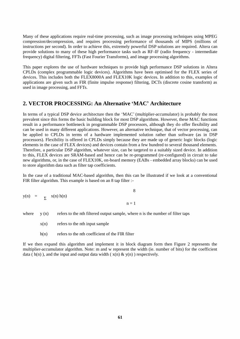
61
Many of these applications require real-time processing, such as image processing techniques using MPEG compression/decompression, and requires processing performance of thousands of MIPS (millions of instructions per second). In order to achieve this, extremely powerful DSP solutions are required. Altera can provide solutions to many of these high performance tasks such as RF-IF (radio frequency - intermediate frequency) digital filtering, FFTs (Fast Fourier Transforms), and image processing algorithms. This paper explores the use of hardware techniques to provide high performance DSP solutions in Altera CPLDs (complex programmable logic devices). Algorithms have been optimised for the FLEX series of devices. This includes both the FLEX8000A and FLEX10K logic devices. In addition to this, examples of applications are given such as FIR (finite impulse response) filtering, DCTs (discrete cosine transform) as used in image processing, and FFTs. 2. VECTOR PROCESSING: An Alternative ‘MAC’ Architecture In terms of a typical DSP device architecture then the ‘MAC’ (multiplier-accumulator) is probably the most prevalent since this forms the basic building block for most DSP algorithms. However, these MAC functions result in a performance bottleneck in programmable DSP processors, although they do offer flexibility and can be used in many different applications. However, an alternative technique, that of vector processing, can be applied to CPLDs in terms of a hardware implemented solution rather than software (as in DSP processors). Flexibility is offered in CPLDs simply because they are made up of generic logic blocks (logic elements in the case of FLEX devices) and devices contain from a few hundred to several thousand elements. Therefore, a particular DSP algorithm, whatever size, can be targeted to a suitably sized device. In addition to this, FLEX devices are SRAM-based and hence can be re-programmed (re-configured) in circuit to take new algorithms, or, in the case of FLEX10K, on-board memory (EABs - embedded array blocks) can be used to store algorithm data such as filter tap coefficients. In the case of a traditional MAC-based algorithm, then this can be illustrated if we look at a conventional FIR filter algorithm. This example is based on an 8 tap filter :- 8 y(n) = Σ x(n) h(n)
n = 1 where y (n) refers to the nth filtered output sample, where n is the number of filter taps x(n) refers to the nth input sample h(n) refers to the nth coefficient of the FIR filter If we then expand this algorithm and implement it in block diagram form then Figure 2 represents the multiplier-accumulator algorithm. Note: m and w represent the width (ie. number of bits) for the coefficient data ( h(n) ), and the input and output data width ( x(n) & y(n) ) respectively.
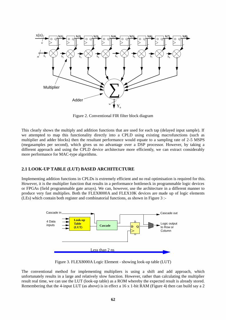
62
x(n)
∑Yn
h1 h4h3h2
D Q D Q D Q D QX(1) X(2) X(3) X(4)
h5 h8h7h6
D Q D Q D Q D QX(5) X(6) X(7) X(8)
w
m
w
Multiplier
Adder
Figure 2. Conventional FIR filter block diagram
This clearly shows the multiply and addition functions that are used for each tap (delayed input sample). If we attempted to map this functionality directly into a CPLD using existing macrofunctions (such as multiplier and adder blocks) then the resultant performance would equate to a sampling rate of 2-5 MSPS (megasamples per second), which gives us no advantage over a DSP processor. However, by taking a different approach and using the CPLD device architecture more efficiently, we can extract considerably more performance for MAC-type algorithms. 2.1 LOOK-UP TABLE (LUT) BASED ARCHITECTURE Implementing addition functions in CPLDs is extremely efficient and no real optimisation is required for this. However, it is the multiplier function that results in a performance bottleneck in programmable logic devices or FPGAs (field programmable gate arrays). We can, however, use the architecture in a different manner to produce very fast multiplies. Both the FLEX8000A and FLEX10K devices are made up of logic elements (LEs) which contain both register and combinatorial functions, as shown in Figure 3 :-
4 Datainputs
Cascade in Cascade out
Logic outputto Row orColumn
D Q
Look-upTable(LUT) Cascade
Less than 2 ns
Figure 3. FLEX8000A Logic Element - showing look-up table (LUT)
The conventional method for implementing multipliers is using a shift and add approach, which unfortunately results in a large and relatively slow function. However, rather than calculating the multiplier result real time, we can use the LUT (look-up table) as a ROM whereby the expected result is already stored. Remembering that the 4-input LUT (as above) is in effect a 16 x 1-bit RAM (Figure 4) then can build say a 2
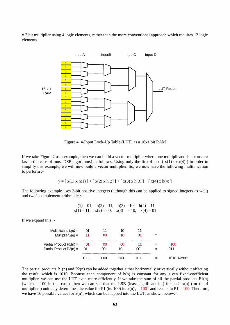
63
x 2 bit multiplier using 4 logic elements, rather than the more conventional approach which requires 12 logic elements.
0
0
0
0
0
1
0
1
0
0
0
0
0
1
0
1
InputA InputB InputC Input D
LUT Result16 x 1 RAM
Figure 4. 4-Input Look-Up Table (LUT) as a 16x1 bit RAM
If we take Figure 2 as a example, then we can build a vector multiplier where one multiplicand is a constant (as in the case of most DSP algorithms) as follows. Using only the first 4 taps ( x(1) to x(4) ) in order to simplify this example, we will now build a vector multiplier. So, we now have the following multiplication to perform :-
y = [ x(1) x h(1) ] + [ x(2) x h(2) ] + [ x(3) x h(3) ] + [ x(4) x h(4) ] The following example uses 2-bit positive integers (although this can be applied to signed integers as well) and two’s complement arithmetic :-
h(1) = 01, h(2) = 11, h(3) = 10, h(4) = 11 x(1) = 11, x(2) = 00, x(3) = 10, x(4) = 01
If we expand this :-
Multiplicand h(n) = 01 11 10 11 Multiplier x(n) = 11 00 10 01 *
------------------------------------------------------------ Partial Product P1(n) = 01 00 00 11 = 100 Partial Product P2(n) = 01 00 10 00 = 011
------------------------------------------------------------ 011 000 100 011 = 1010 Result
The partial products P1(n) and P2(n) can be added together either horizontally or vertically without affecting the result, which is 1010. Because each component of h(n) is constant for any given fixed-coefficient multiplier, we can use the LUT even more efficiently. If we take the sum of all the partial products P1(n) (which is 100 in this case), then we can see that the LSB (least significant bit) for each x(n) (for the 4 multipliers) uniquely determines the value for P1 (ie. 100) ie. x(n)1 = 1001 and results in P1 = 100. Therefore, we have 16 possible values for x(n)1 which can be mapped into the LUT, as shown below:-
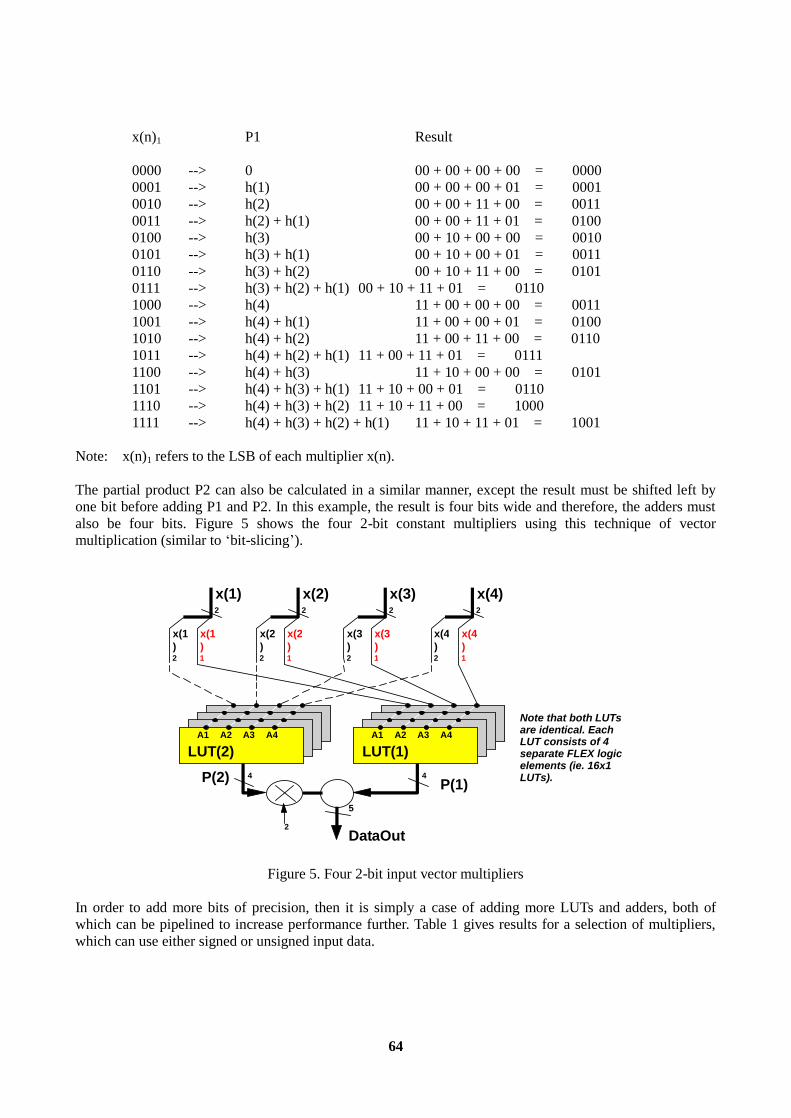
64
x(n)1 P1 Result 0000 --> 0 00 + 00 + 00 + 00 = 0000 0001 --> h(1) 00 + 00 + 00 + 01 = 0001 0010 --> h(2) 00 + 00 + 11 + 00 = 0011 0011 --> h(2) + h(1) 00 + 00 + 11 + 01 = 0100 0100 --> h(3) 00 + 10 + 00 + 00 = 0010 0101 --> h(3) + h(1) 00 + 10 + 00 + 01 = 0011 0110 --> h(3) + h(2) 00 + 10 + 11 + 00 = 0101 0111 --> h(3) + h(2) + h(1) 00 + 10 + 11 + 01 = 0110 1000 --> h(4) 11 + 00 + 00 + 00 = 0011 1001 --> h(4) + h(1) 11 + 00 + 00 + 01 = 0100 1010 --> h(4) + h(2) 11 + 00 + 11 + 00 = 0110 1011 --> h(4) + h(2) + h(1) 11 + 00 + 11 + 01 = 0111 1100 --> h(4) + h(3) 11 + 10 + 00 + 00 = 0101 1101 --> h(4) + h(3) + h(1) 11 + 10 + 00 + 01 = 0110 1110 --> h(4) + h(3) + h(2) 11 + 10 + 11 + 00 = 1000 1111 --> h(4) + h(3) + h(2) + h(1) 11 + 10 + 11 + 01 = 1001 Note: x(n)1 refers to the LSB of each multiplier x(n). The partial product P2 can also be calculated in a similar manner, except the result must be shifted left by one bit before adding P1 and P2. In this example, the result is four bits wide and therefore, the adders must also be four bits. Figure 5 shows the four 2-bit constant multipliers using this technique of vector multiplication (similar to ‘bit-slicing’).
Note that both LUTsare identical. EachLUT consists of 4separate FLEX logicelements (ie. 16x1LUTs).
x(2)
x(2)1
x(2)2
x(3)
x(3)1
x(3)2
x(4)
x(4)1
x(4)2
LUT(2)A1 A2 A3 A4
LUT(1)A1 A2 A3 A4
x(1)
x(1)1
x(1)2
4 4P(1)P(2)
DataOut
2
5
2 2 2
2
Figure 5. Four 2-bit input vector multipliers In order to add more bits of precision, then it is simply a case of adding more LUTs and adders, both of which can be pipelined to increase performance further. Table 1 gives results for a selection of multipliers, which can use either signed or unsigned input data.
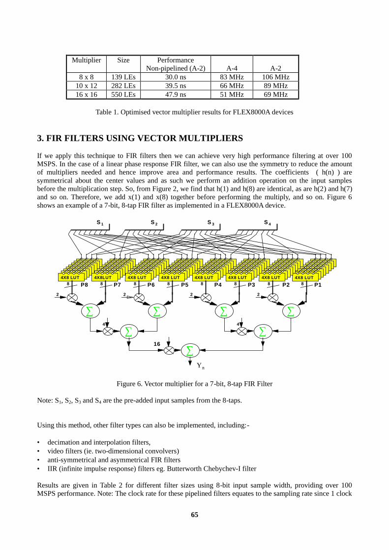
65
Multiplier Size Performance Non-pipelined (A-2)
A-4
A-2
8 x 8 139 LEs 30.0 ns 83 MHz 106 MHz 10 x 12 282 LEs 39.5 ns 66 MHz 89 MHz 16 x 16 550 LEs 47.9 ns 51 MHz 69 MHz
Table 1. Optimised vector multiplier results for FLEX8000A devices
3. FIR FILTERS USING VECTOR MULTIPLIERS If we apply this technique to FIR filters then we can achieve very high performance filtering at over 100 MSPS. In the case of a linear phase response FIR filter, we can also use the symmetry to reduce the amount of multipliers needed and hence improve area and performance results. The coefficients ( h(n) ) are symmetrical about the center values and as such we perform an addition operation on the input samples before the multiplication step. So, from Figure 2, we find that h(1) and h(8) are identical, as are h(2) and h(7) and so on. Therefore, we add x(1) and x(8) together before performing the multiply, and so on. Figure 6 shows an example of a 7-bit, 8-tap FIR filter as implemented in a FLEX8000A device.
4X8 LUT 4X8LUT 4X8 LUT 4X8 LUT 4X8 LUT 4X8 LUT4X8 LUT 4X8 LUT8 8 8 8 8 8 8 8
S 1 S 2 S 3 S 4
∑
2
∑
2
∑
2
∑
2
∑4
∑4
∑16
P1P5 P4 P3 P2P8 P7 P6
Yn
Figure 6. Vector multiplier for a 7-bit, 8-tap FIR Filter Note: S1, S2, S3 and S4 are the pre-added input samples from the 8-taps. Using this method, other filter types can also be implemented, including:- • decimation and interpolation filters, • video filters (ie. two-dimensional convolvers) • anti-symmetrical and asymmetrical FIR filters • IIR (infinite impulse response) filters eg. Butterworth Chebychev-I filter Results are given in Table 2 for different filter sizes using 8-bit input sample width, providing over 100 MSPS performance. Note: The clock rate for these pipelined filters equates to the sampling rate since 1 clock
66
cycle provides 1 output result.
Filter Type Input
Precision Internal
Precision Output
Precision Size Performance
A-4
A-2 8 8 17 17 296 66 MSPS 101 MSPS 16 8 10 10 468 75 MSPS 101 MSPS 24 8 10 10 653 74 MSPS 100 MSPS 32 8 10 10 862 75 MSPS 101 MSPS
Table 2. FIR Filter Performance & Size in FLEX8000A Devices
4. IMAGE PROCESSING USING VECTOR MULTIPLIERS Digital image processing encompasses a wide range of applications from medical imaging and satellite image processing to more traditional areas such as radar and sonar processing systems. For many of these applications, including such standards as JPEG and MPEG, there are numerous standard chipsets available now or in the near future. However, programmable logic such as the FLEX10K in particular, has plenty to offer in this field. There are many applications where unique requirements dictate that a custom solution be provided. Examples include :- • Non-standard frame sizes - eg. some medical applications involve image sizes up to 4K x 4K pixels (non-interlaced). • Frame rates - processing may be required in excess of 30 frames per second, such as when real time, or accelerated processing of high speed (slow motion) image sequences is needed. • Other operations - such as image re-sizing, may be required at the same time as compression. Both operations can be performed during the processing of the transform, rather than separately. • Image format conversion. The Altera FLEX10K family is particularly suitable for image processing applications, since it offers an embedded array block (EAB), which can be configured as a fast static RAM with up to 80MHz throughput. The EAB can in fact be configured to provide a 256 x 8-bit RAM which is the same size as an MPEG macroblock (ie. with two luminance and two chrominance blocks - 4:2:2 format). For other standards, four 8 x 8, or one 16 x 16 pixel block can be stored in one EAB. Additionally, four DCT quantisation tables, or a JPEG or MPEG Huffman coding table can fit into one EAB. The EAB also offers the capability of storing intermediate values during processing of certain transforms, as we can see below in the case of the DCT (Discrete Cosine Transform). 4.1 OPTIMISED DCT FOR USE IN FLEX10K The DCT is used in many image processing standards (eg. MPEG and JPEG) and as such is used to convert image data into the frequency domain before applying such techniques as image compression or re-quantisation. A standard DCT requires of the order of 2048 ‘software-equivalent’ operations to complete. There are a number of optimised solutions, for example Feig’s algorithm which requires only 556 operations. However, Altera have produced an optimised hardware version, using the technique of vector multipliers, that takes only 400 operations and is hence faster. For a two dimensional DCT algorithm, the formula is as follows :-
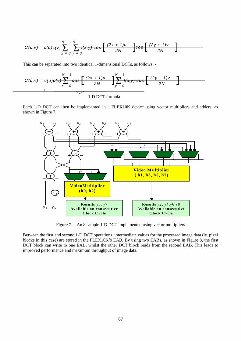
67
C(u,v) = c(u)c(v) ΣN 1
x = 0f(x,y) cos cosΣ
N 1
y = 0
(2x + 1)uπ2N[ ] (2y + 1)vπ
2N[ ]
This can be separated into two identical 1-dimensional DCTs, as follows :-
= c(u)c(v) ΣN 1
x = 0cos (2x + 1)uπ
2N[ ] f(x,y) cosΣN 1
y = 0
(2y + 1)vπ2N[ ]C(u,v)
1-D DCT formula Each 1-D DCT can then be implemented in a FLEX10K device using vector multipliers and adders, as shown in Figure 7.
s 4 s 5s 3 s 6s 2 s 7s 1 s 8
Video M ultiplier( h1, h3, h5, h7)
y 1 y 5
V e c to r M u ltip lie r
R esults y3, y7Available on consecutive
C lock C ycle
R esults y2, y4 ,y6 ,y8Available on consecutive
C lock C ycle
h 4
VideoM ultiplier(h0, h2)
Figure 7. An 8 sample 1-D DCT implemented using vector multipliers Between the first and second 1-D DCT operations, intermediate values for the processed image data (ie. pixel blocks in this case) are stored in the FLEX10K’s EAB. By using two EABs, as shown in Figure 8, the first DCT block can write to one EAB, whilst the other DCT block reads from the second EAB. This leads to improved performance and maximum throughput of image data.
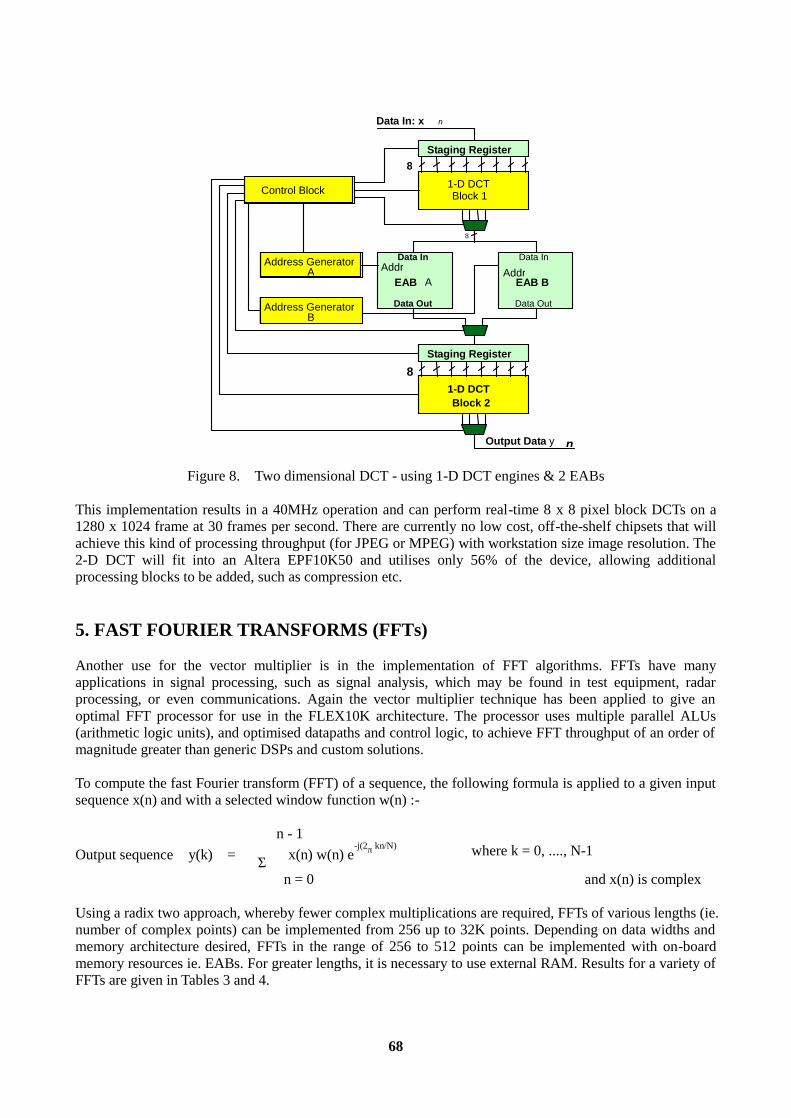
68
8
8
1-D DCTBlock 1
Staging Register
EAB A
Data InAddr Addr
Control Block
8Staging Register
Address GeneratorA
Output Data y n
Data In: x n
Address GeneratorB
EAB B
1-D DCTBlock 2
Data Out
Data In
Data Out
Figure 8. Two dimensional DCT - using 1-D DCT engines & 2 EABs This implementation results in a 40MHz operation and can perform real-time 8 x 8 pixel block DCTs on a 1280 x 1024 frame at 30 frames per second. There are currently no low cost, off-the-shelf chipsets that will achieve this kind of processing throughput (for JPEG or MPEG) with workstation size image resolution. The 2-D DCT will fit into an Altera EPF10K50 and utilises only 56% of the device, allowing additional processing blocks to be added, such as compression etc. 5. FAST FOURIER TRANSFORMS (FFTs) Another use for the vector multiplier is in the implementation of FFT algorithms. FFTs have many applications in signal processing, such as signal analysis, which may be found in test equipment, radar processing, or even communications. Again the vector multiplier technique has been applied to give an optimal FFT processor for use in the FLEX10K architecture. The processor uses multiple parallel ALUs (arithmetic logic units), and optimised datapaths and control logic, to achieve FFT throughput of an order of magnitude greater than generic DSPs and custom solutions. To compute the fast Fourier transform (FFT) of a sequence, the following formula is applied to a given input sequence x(n) and with a selected window function w(n) :- n - 1 Output sequence y(k) = Σ x(n) w(n) e
-j(2π kn/N) where k = 0, ...., N-1
n = 0 and x(n) is complex Using a radix two approach, whereby fewer complex multiplications are required, FFTs of various lengths (ie. number of complex points) can be implemented from 256 up to 32K points. Depending on data widths and memory architecture desired, FFTs in the range of 256 to 512 points can be implemented with on-board memory resources ie. EABs. For greater lengths, it is necessary to use external RAM. Results for a variety of FFTs are given in Tables 3 and 4.
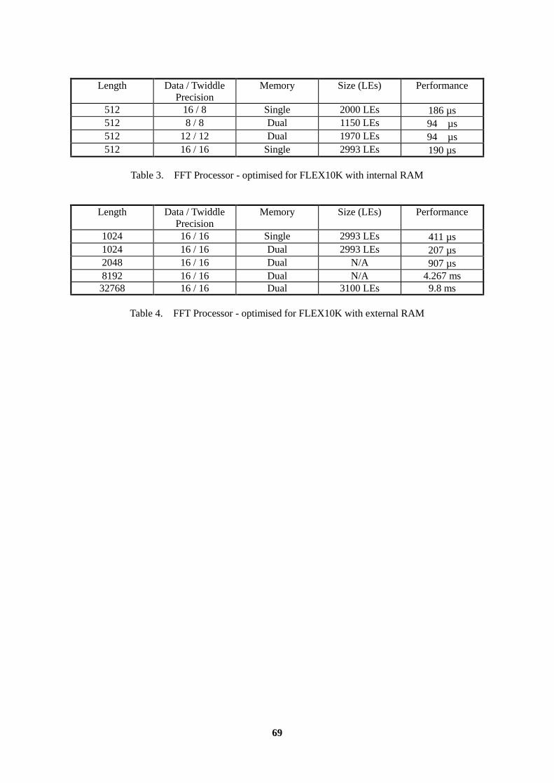
69
Length
Data / Twiddle Precision
Memory Size (LEs) Performance
512 16 / 8 Single 2000 LEs 186 µs 512 8 / 8 Dual 1150 LEs 94 µs 512 12 / 12 Dual 1970 LEs 94 µs 512 16 / 16 Single 2993 LEs 190 µs
Table 3. FFT Processor - optimised for FLEX10K with internal RAM
Length
Data / Twiddle Precision
Memory Size (LEs) Performance
1024 16 / 16 Single 2993 LEs 411 µs 1024 16 / 16 Dual 2993 LEs 207 µs 2048 16 / 16 Dual N/A 907 µs 8192 16 / 16 Dual N/A 4.267 ms
32768 16 / 16 Dual 3100 LEs 9.8 ms
Table 4. FFT Processor - optimised for FLEX10K with external RAM

70
CONCLUSION We have seen that using a novel hardware approach to DSP algorithms, we can in fact extract considerably more performance out of a CPLD than we could if we used DSP processors or indeed custom ASIC solutions. Using this vector multiplier, we can provide the basic building block for numerous applications, such as FIR filtering, Fast Fourier Transforms (FFTs) and Discrete Cosine Transforms (DCTs). There are indeed many other examples where, in addition to replacing DSP chipsets for certain functions, we can also use programmable logic to off-load some of the signal processing and improve the overall throughput of the system. For more information on any of these applications, please refer to the Altera DSP Design Kit or contact Altera directly. REFERENCES 1. Speed Optimised FIR Filters in FLEX8000 Devices by Simon Redmile (1995). 2. Altera DSP Design Kit version 1.0 (1995). 3. Digital Signal Processing by Oktay Alkin (1994). 4. Automated FFT Processor Design by Martin Langhammer & Caleb Crome (1996). 5. Image Processing In Altera FLEX10K Devices by Caleb Crome ( 1996). 6. CPLD Methods For Fast, Economical DSP by Simon Redmile & Doug Amos (1995).
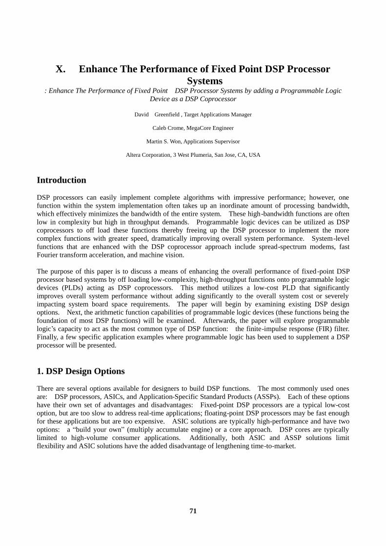
71
X. Enhance The Performance of Fixed Point DSP Processor
Systems : Enhance The Performance of Fixed Point DSP Processor Systems by adding a Programmable Logic
Device as a DSP Coprocessor
David Greenfield , Target Applications Manager
Caleb Crome, MegaCore Engineer
Martin S. Won, Applications Supervisor
Altera Corporation, 3 West Plumeria, San Jose, CA, USA Introduction DSP processors can easily implement complete algorithms with impressive performance; however, one function within the system implementation often takes up an inordinate amount of processing bandwidth, which effectively minimizes the bandwidth of the entire system. These high-bandwidth functions are often low in complexity but high in throughput demands. Programmable logic devices can be utilized as DSP coprocessors to off load these functions thereby freeing up the DSP processor to implement the more complex functions with greater speed, dramatically improving overall system performance. System-level functions that are enhanced with the DSP coprocessor approach include spread-spectrum modems, fast Fourier transform acceleration, and machine vision. The purpose of this paper is to discuss a means of enhancing the overall performance of fixed-point DSP processor based systems by off loading low-complexity, high-throughput functions onto programmable logic devices (PLDs) acting as DSP coprocessors. This method utilizes a low-cost PLD that significantly improves overall system performance without adding significantly to the overall system cost or severely impacting system board space requirements. The paper will begin by examining existing DSP design options. Next, the arithmetic function capabilities of programmable logic devices (these functions being the foundation of most DSP functions) will be examined. Afterwards, the paper will explore programmable logic’s capacity to act as the most common type of DSP function: the finite-impulse response (FIR) filter. Finally, a few specific application examples where programmable logic has been used to supplement a DSP processor will be presented. 1. DSP Design Options There are several options available for designers to build DSP functions. The most commonly used ones are: DSP processors, ASICs, and Application-Specific Standard Products (ASSPs). Each of these options have their own set of advantages and disadvantages: Fixed-point DSP processors are a typical low-cost option, but are too slow to address real-time applications; floating-point DSP processors may be fast enough for these applications but are too expensive. ASIC solutions are typically high-performance and have two options: a “build your own” (multiply accumulate engine) or a core approach. DSP cores are typically limited to high-volume consumer applications. Additionally, both ASIC and ASSP solutions limit flexibility and ASIC solutions have the added disadvantage of lengthening time-to-market.
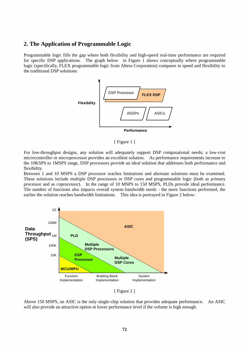
72
2. The Application of Programmable Logic Programmable logic fills the gap where both flexibility and high-speed real-time performance are required for specific DSP applications. The graph below in Figure 1 shows conceptually where programmable logic (specifically, FLEX programmable logic from Altera Corporation) compares in speed and flexibility to the traditional DSP solutions:
Flexibility
FLEX DSP
ASSPs
Performance
DSP Processor
ASICs
[ Figure 1 ] For low-throughput designs, any solution will adequately support DSP computational needs; a low-cost microcontroller or microprocessor provides an excellent solution. As performance requirements increase to the 10KSPS to 1MSPS range, DSP processors provide an ideal solution that addresses both performance and flexibility. Between 1 and 10 MSPS a DSP processor reaches limitations and alternate solutions must be examined. These solutions include multiple DSP processors or DSP cores and programmable logic (both as primary processor and as coprocessor). In the range of 10 MSPS to 150 MSPS, PLDs provide ideal performance. The number of functions also impacts overall system bandwidth needs - the more functions performed, the earlier the solution reaches bandwidth limitations. This idea is portrayed in Figure 2 below:
DataThroughput(SPS)
SystemImplementation
Building BlockImplementation
FunctionImplementation
10K
1M
100K
100M
1G
ASIC
DSPProcessor
MCU/MPU
MultipleDSP Processors
MultipleDSP Cores
PLD
[ Figure 2 ] Above 150 MSPS, an ASIC is the only single-chip solution that provides adequate performance. An ASIC will also provide an attractive option at lower performance level if the volume is high enough.
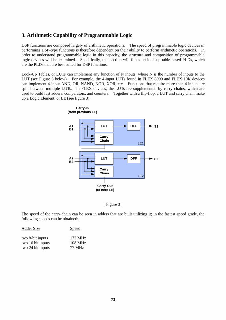
73
3. Arithmetic Capability of Programmable Logic DSP functions are composed largely of arithmetic operations. The speed of programmable logic devices in performing DSP-type functions is therefore dependent on their ability to perform arithmetic operations. In order to understand programmable logic in this capacity, the structure and composition of programmable logic devices will be examined. Specifically, this section will focus on look-up table-based PLDs, which are the PLDs that are best suited for DSP functions. Look-Up Tables, or LUTs can implement any function of N inputs, where N is the number of inputs to the LUT (see Figure 3 below). For example, the 4-input LUTs found in FLEX 8000 and FLEX 10K devices can implement 4-input AND, OR, NAND, NOR, XOR, etc. Functions that require more than 4 inputs are split between multiple LUTs. In FLEX devices, the LUTs are supplemented by carry chains, which are used to build fast adders, comparators, and counters. Together with a flip-flop, a LUT and carry chain make up a Logic Element, or LE (see figure 3).
LUT
CarryChain
DFF
Carry-In(from previous LE)
S1
LE1
LUT
CarryChain
DFF S2
LE2
A1B1
A2B2
Carry-Out(to next LE)
[ Figure 3 ] The speed of the carry-chain can be seen in adders that are built utilizing it; in the fastest speed grade, the following speeds can be obtained: Adder Size Speed two 8-bit inputs 172 MHz two 16 bit inputs 108 MHz two 24 bit inputs 77 MHz
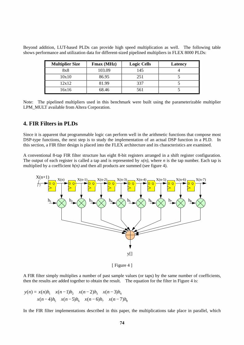
74
Beyond addition, LUT-based PLDs can provide high speed multiplication as well. The following table shows performance and utilization data for different-sized pipelined multipliers in FLEX 8000 PLDs:
Multiplier Size Fmax (MHz) Logic Cells Latency 8x8 103.09 145 4
10x10 86.95 251 5 12x12 81.99 337 5 16x16 68.46 561 5
Note: The pipelined multipliers used in this benchmark were built using the parameterizable multiplier LPM_MULT available from Altera Corporation. 4. FIR Filters in PLDs Since it is apparent that programmable logic can perform well in the arithmetic functions that compose most DSP-type functions, the next step is to study the implementation of an actual DSP function in a PLD. In this section, a FIR filter design is placed into the FLEX architecture and its characteristics are examined. A conventional 8-tap FIR filter structure has eight 8-bit registers arranged in a shift register configuration. The output of each register is called a tap and is represented by x(n), where n is the tap number. Each tap is multiplied by a coefficient h(n) and then all products are summed (see figure 4).
X(n-7)
h1 h4h3h2
X(n+1)D Q7
X(n) X(n-1) X(n-2) X(n-3) X(n-4) X(n-5) X(n-6)
h5 h8h7h6
y[]
D Q D Q D Q D Q D QD Q D Q
[ Figure 4 ] A FIR filter simply multiplies a number of past sample values (or taps) by the same number of coefficients, then the results are added together to obtain the result. The equation for the filter in Figure 4 is: y n x n h x n h x n h x n h
x n h x n h x n h x n h( ) ( ) ( ) ( ) ( )
( ) ( ) ( ) ( )= + − + − + − +
− + − + − + −1 2 3 4
5 6 7 8
1 2 34 5 6 7
In the FIR filter implementations described in this paper, the multiplications take place in parallel, which
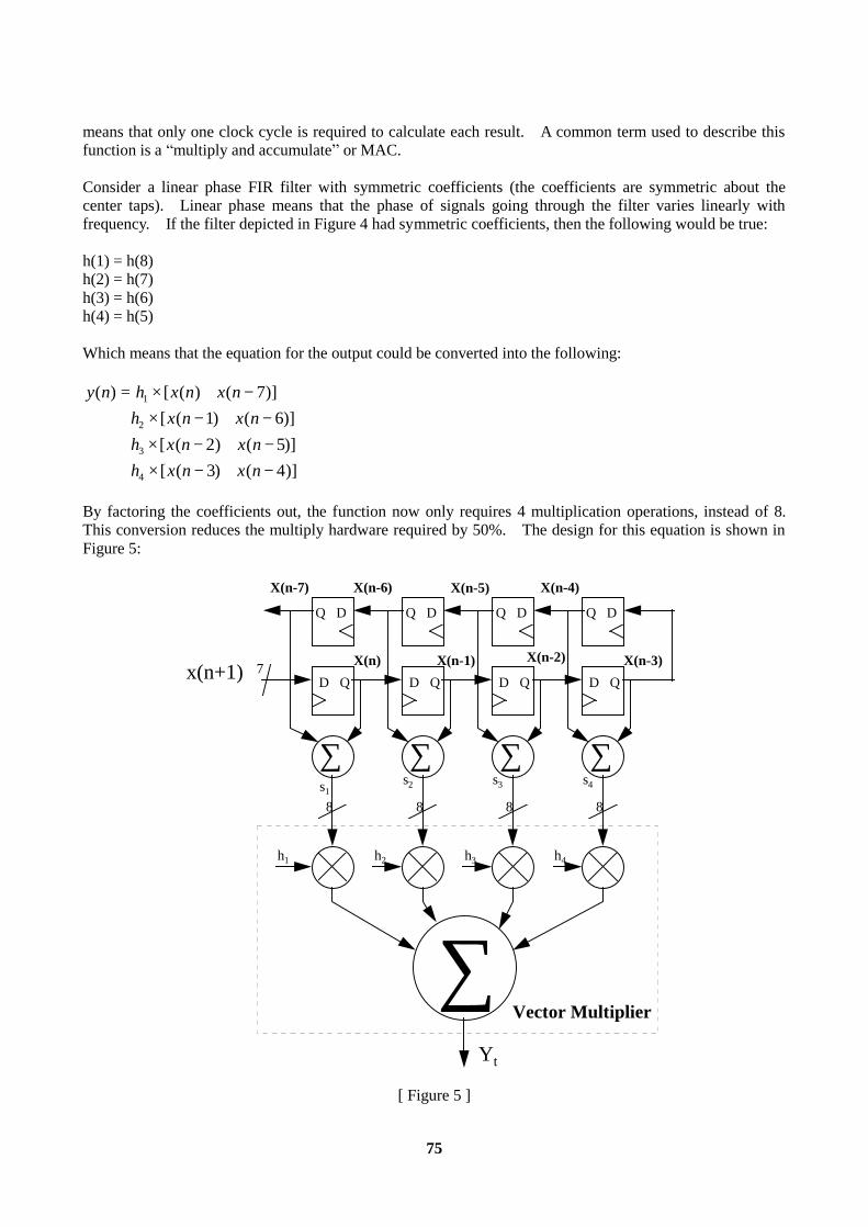
75
means that only one clock cycle is required to calculate each result. A common term used to describe this function is a “multiply and accumulate” or MAC. Consider a linear phase FIR filter with symmetric coefficients (the coefficients are symmetric about the center taps). Linear phase means that the phase of signals going through the filter varies linearly with frequency. If the filter depicted in Figure 4 had symmetric coefficients, then the following would be true: h(1) = h(8) h(2) = h(7) h(3) = h(6) h(4) = h(5) Which means that the equation for the output could be converted into the following: y n h x n x n
h x n x nh x n x nh x n x n
( ) [ ( ) ( )][ ( ) ( )][ ( ) ( )][ ( ) ( )]
= × + − +× − + − +× − + − +× − + −
1
2
3
4
71 62 53 4
By factoring the coefficients out, the function now only requires 4 multiplication operations, instead of 8. This conversion reduces the multiply hardware required by 50%. The design for this equation is shown in Figure 5:
h1 h4h3h2
∑Yt
x(n+1) D Q D Q D Q D Q7
DQDQDQDQ
∑ ∑∑∑s1
s4s3s2
8 8 8 8
Vector Multiplier
X(n) X(n-1) X(n-2) X(n-3)
X(n-4)X(n-5)X(n-6)X(n-7)
[ Figure 5 ]
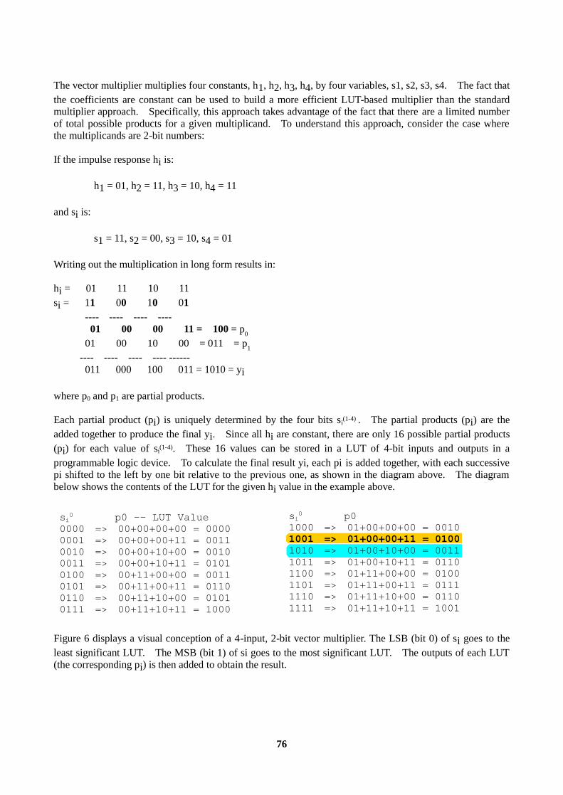
76
The vector multiplier multiplies four constants, h1, h2, h3, h4, by four variables, s1, s2, s3, s4. The fact that the coefficients are constant can be used to build a more efficient LUT-based multiplier than the standard multiplier approach. Specifically, this approach takes advantage of the fact that there are a limited number of total possible products for a given multiplicand. To understand this approach, consider the case where the multiplicands are 2-bit numbers: If the impulse response hi is: h1 = 01, h2 = 11, h3 = 10, h4 = 11 and si is: s1 = 11, s2 = 00, s3 = 10, s4 = 01 Writing out the multiplication in long form results in: hi = 01 11 10 11 si = 11 00 10 01 ---- ---- ---- ---- 01 00 00 11 = 100 = p0 01 00 10 00 = 011 = p1 ---- ---- ---- ---- ------ 011 000 100 011 = 1010 = yi where p0 and p1 are partial products. Each partial product (pi) is uniquely determined by the four bits si(1-4)
. The partial products (pi) are the added together to produce the final yi. Since all hi are constant, there are only 16 possible partial products (pi) for each value of si(1-4). These 16 values can be stored in a LUT of 4-bit inputs and outputs in a programmable logic device. To calculate the final result yi, each pi is added together, with each successive pi shifted to the left by one bit relative to the previous one, as shown in the diagram above. The diagram below shows the contents of the LUT for the given hi value in the example above.
si0 p01000 => 01+00+00+00 = 00101001 => 01+00+00+11 = 01001010 => 01+00+10+00 = 00111011 => 01+00+10+11 = 01101100 => 01+11+00+00 = 01001101 => 01+11+00+11 = 01111110 => 01+11+10+00 = 01101111 => 01+11+10+11 = 1001
si0 p0 -- LUT Value0000 => 00+00+00+00 = 00000001 => 00+00+00+11 = 00110010 => 00+00+10+00 = 00100011 => 00+00+10+11 = 01010100 => 00+11+00+00 = 00110101 => 00+11+00+11 = 01100110 => 00+11+10+00 = 01010111 => 00+11+10+11 = 1000
Figure 6 displays a visual conception of a 4-input, 2-bit vector multiplier. The LSB (bit 0) of si goes to the least significant LUT. The MSB (bit 1) of si goes to the most significant LUT. The outputs of each LUT (the corresponding pi) is then added to obtain the result.
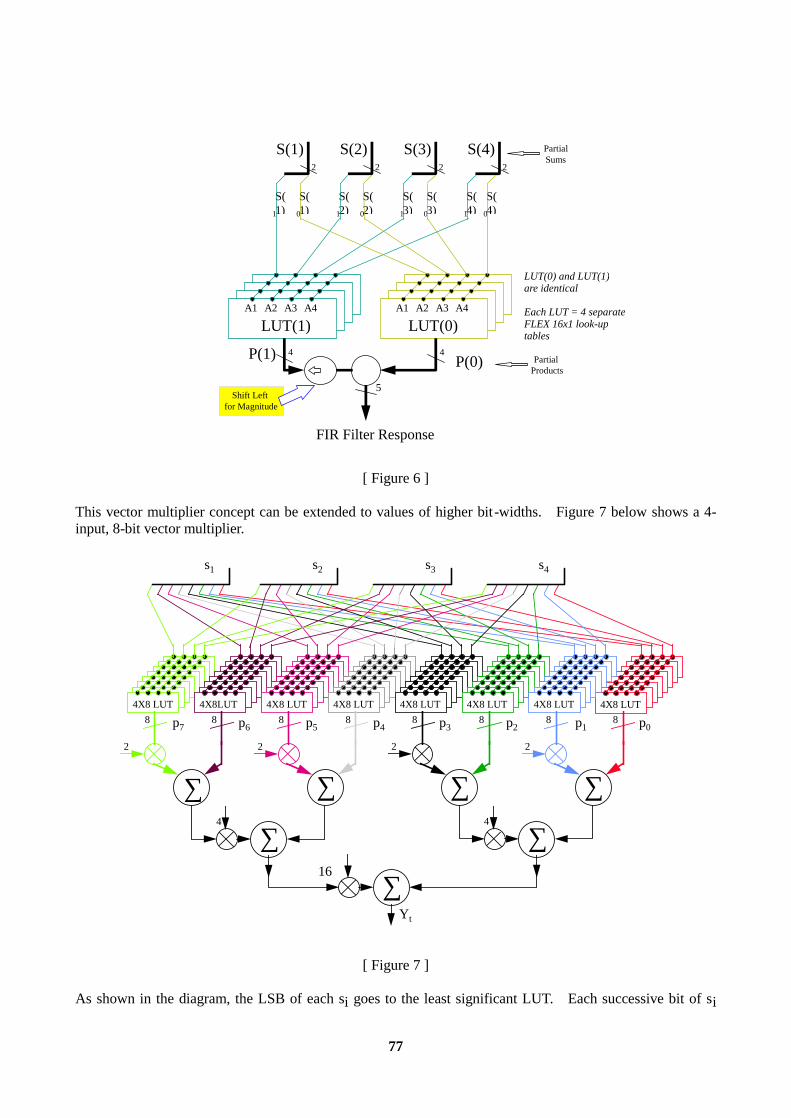
77
LUT(0) and LUT(1)are identical
Each LUT = 4 separateFLEX 16x1 look-uptables
PartialSums
LUT(1)A1 A2 A3 A4
LUT(0)A1 A2 A3 A4
4 4P(0)P(1)
1
FIR Filter Response
5
S(3) S(4)
S(4)0
S(4)1
S(2)
S(2)0
S(2)1
S(3)0
S(3)1
S(1)
S(1)0
S(1)1
2 2 2 2
Shift Leftfor Magnitude
PartialProducts
[ Figure 6 ]
This vector multiplier concept can be extended to values of higher bit -widths. Figure 7 below shows a 4-input, 8-bit vector multiplier.
4X8 LUT 4X8LUT 4X8 LUT 4X8 LUT 4X8 LUT 4X8 LUT4X8 LUT 4X8 LUT8 8 8 8 8 8 8 8
s1 s2 s3 s4
∑
2
∑
2
∑
2
∑
2
∑4
∑4
∑16
p0p4 p3 p2 p1p7 p6 p5
Yt
[ Figure 7 ] As shown in the diagram, the LSB of each si goes to the least significant LUT. Each successive bit of si
78
goes to the LUT that is one bit more significant. The outputs of each LUT are then shifted & added for final result. As an example, suppose that each pi happens to be FFh or 11111111b. The addition of all 8 pis would then be broken down into 4 sets of 2 input additions: 11111111 11111111 ——————————— 1011111101 The results of these 4 additions becomes 2 sets of additions: 1011111101 1011111101 ——————————— 111011110001 - these 2 results are then added: 111011110001 111011110001 ————————————— 1111111000000001 - which is the final result. 5. Using the Vector Multiplier in FIR Filters Applying the vector multiplier concept to FIR filters allows programmable logic to achieve high performance and low resource utilization. The following table illustrates performance and resource utilization characteristics for several FIR filters implemented in FLEX 8000 programmable logic (the values shown in the column marked “A-2” and “A-3” refer to different speed grades of the devices). FIR Filter Utilization Performance (MSPS) (Logic Cells) A-2 A-3 8-Tap Parallel 296 101 74 16-Tap Parallel 468 101 75 24-Tap Parallel 653 100 74 32-Tap Parallel 862 101 75 64-Tap Serial 920 7 5 The resource utilization of a FIR filter in a PLD grows as both the input value width increases and as the number of taps increases. The following graph shows the relationship between resource utilization and input value width (assuming 8-bit coefficients).
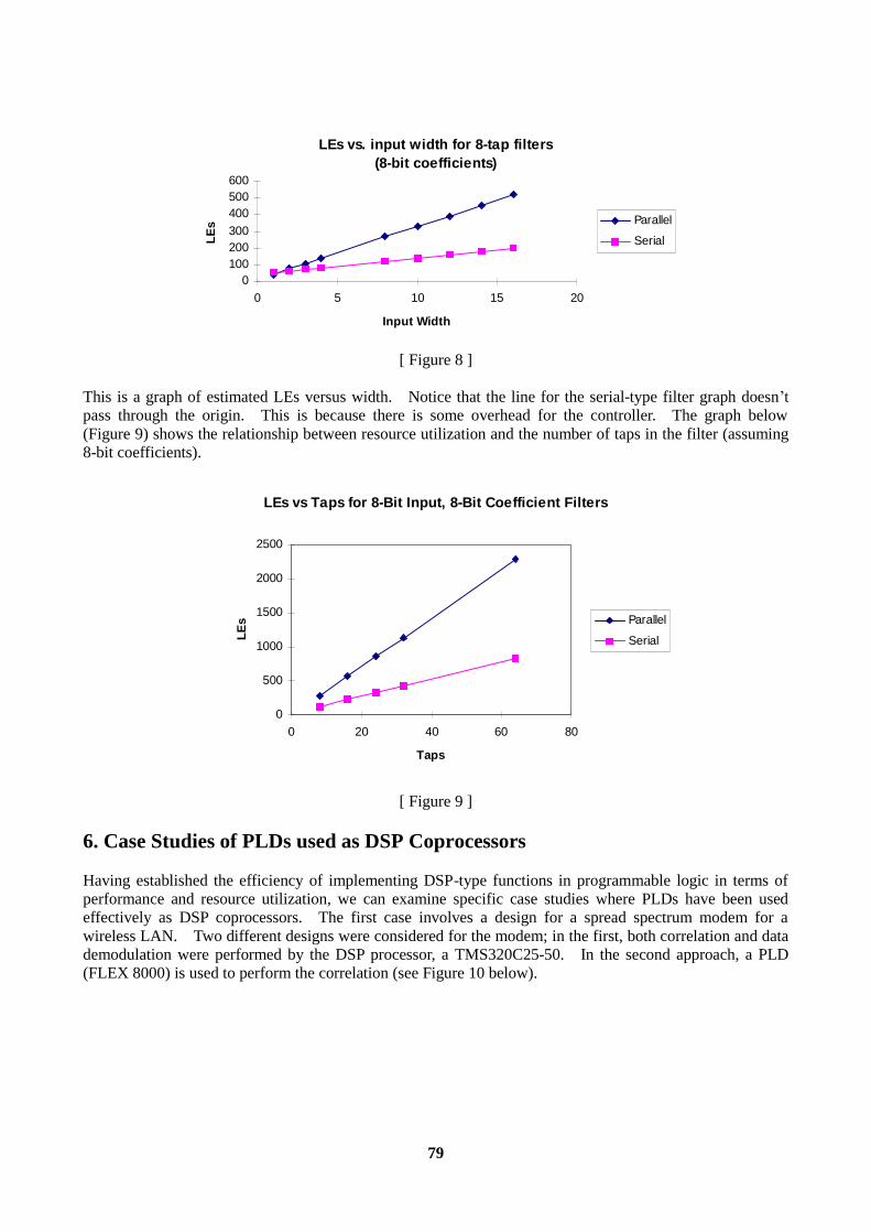
79
LEs vs. input width for 8-tap filters(8-bit coefficients)
0100200300400500600
0 5 10 15 20
Input Width
LEs Parallel
Serial
[ Figure 8 ]
This is a graph of estimated LEs versus width. Notice that the line for the serial-type filter graph doesn’t pass through the origin. This is because there is some overhead for the controller. The graph below (Figure 9) shows the relationship between resource utilization and the number of taps in the filter (assuming 8-bit coefficients).
LEs vs Taps for 8-Bit Input, 8-Bit Coefficient Filters
0
500
1000
1500
2000
2500
0 20 40 60 80
Taps
LEs Parallel
Serial
[ Figure 9 ] 6. Case Studies of PLDs used as DSP Coprocessors Having established the efficiency of implementing DSP-type functions in programmable logic in terms of performance and resource utilization, we can examine specific case studies where PLDs have been used effectively as DSP coprocessors. The first case involves a design for a spread spectrum modem for a wireless LAN. Two different designs were considered for the modem; in the first, both correlation and data demodulation were performed by the DSP processor, a TMS320C25-50. In the second approach, a PLD (FLEX 8000) is used to perform the correlation (see Figure 10 below).
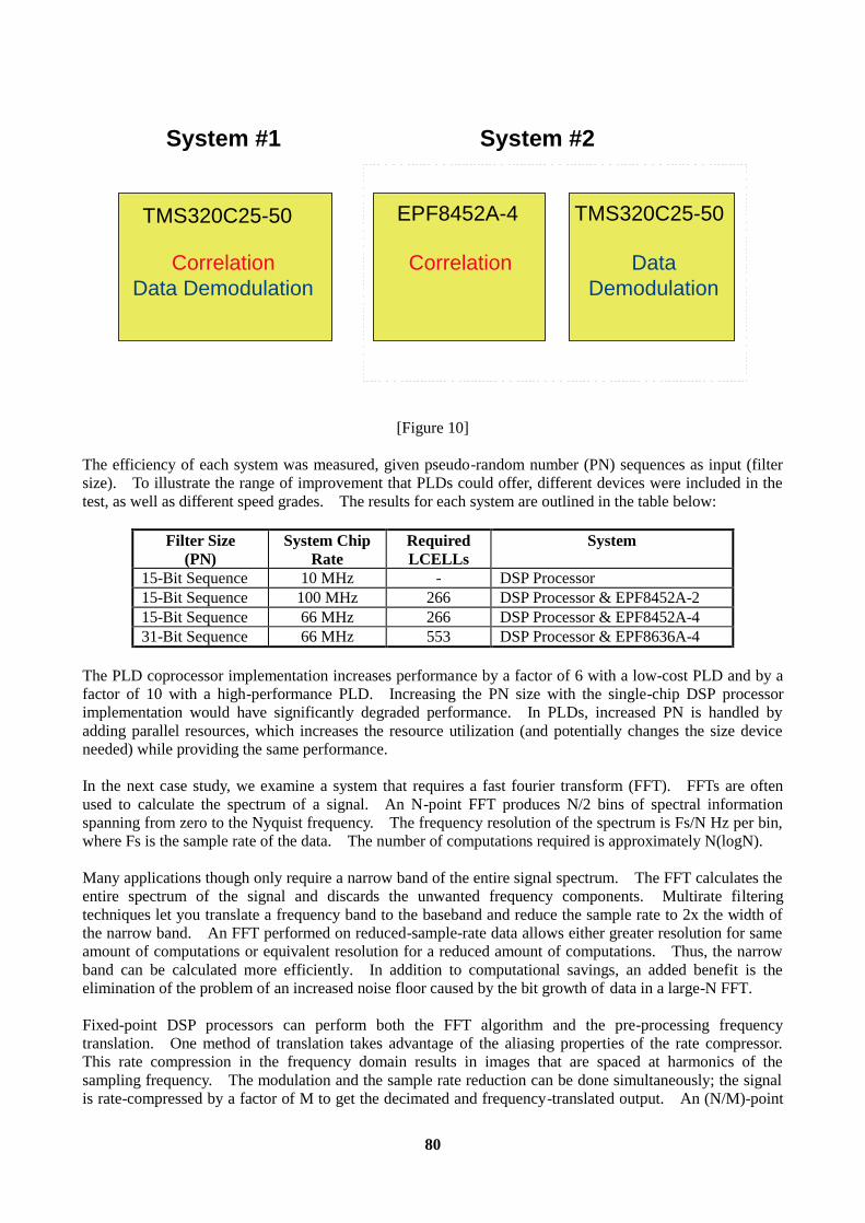
80
System #1
TMS320C25-50
CorrelationData Demodulation
System #2
TMS320C25-50EPF8452A-4
Correlation DataDemodulation
[Figure 10] The efficiency of each system was measured, given pseudo-random number (PN) sequences as input (filter size). To illustrate the range of improvement that PLDs could offer, different devices were included in the test, as well as different speed grades. The results for each system are outlined in the table below:
Filter Size (PN)
System Chip Rate
Required LCELLs
System
15-Bit Sequence 10 MHz - DSP Processor 15-Bit Sequence 100 MHz 266 DSP Processor & EPF8452A-2 15-Bit Sequence 66 MHz 266 DSP Processor & EPF8452A-4 31-Bit Sequence 66 MHz 553 DSP Processor & EPF8636A-4
The PLD coprocessor implementation increases performance by a factor of 6 with a low-cost PLD and by a factor of 10 with a high-performance PLD. Increasing the PN size with the single-chip DSP processor implementation would have significantly degraded performance. In PLDs, increased PN is handled by adding parallel resources, which increases the resource utilization (and potentially changes the size device needed) while providing the same performance. In the next case study, we examine a system that requires a fast fourier transform (FFT). FFTs are often used to calculate the spectrum of a signal. An N-point FFT produces N/2 bins of spectral information spanning from zero to the Nyquist frequency. The frequency resolution of the spectrum is Fs/N Hz per bin, where Fs is the sample rate of the data. The number of computations required is approximately N(logN). Many applications though only require a narrow band of the entire signal spectrum. The FFT calculates the entire spectrum of the signal and discards the unwanted frequency components. Multirate filtering techniques let you translate a frequency band to the baseband and reduce the sample rate to 2x the width of the narrow band. An FFT performed on reduced-sample-rate data allows either greater resolution for same amount of computations or equivalent resolution for a reduced amount of computations. Thus, the narrow band can be calculated more efficiently. In addition to computational savings, an added benefit is the elimination of the problem of an increased noise floor caused by the bit growth of data in a large-N FFT. Fixed-point DSP processors can perform both the FFT algorithm and the pre-processing frequency translation. One method of translation takes advantage of the aliasing properties of the rate compressor. This rate compression in the frequency domain results in images that are spaced at harmonics of the sampling frequency. The modulation and the sample rate reduction can be done simultaneously; the signal is rate-compressed by a factor of M to get the decimated and frequency-translated output. An (N/M)-point
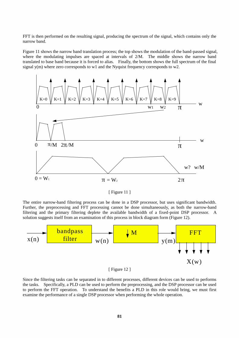
81
FFT is then performed on the resulting signal, producing the spectrum of the signal, which contains only the narrow band. Figure 11 shows the narrow band translation process; the top shows the modulation of the band-passed signal, where the modulating impulses are spaced at intervals of 2/M. The middle shows the narrow band translated to base band because it is forced to alias. Finally, the bottom shows the full spectrum of the final signal y(m) where zero corresponds to w1 and the Nyquist frequency corresponds to w2.
K=0 K=9K=8K=7K=6K=5K=4K=2 K=3K=1
0 w1 w2
π
π
0 /M 2 /Mπ π
w
w
π π0 = W1 = W2 2
w? w/M
[ Figure 11 ] The entire narrow-band filtering process can be done in a DSP processor, but uses significant bandwidth. Further, the preprocessing and FFT processing cannot be done simultaneously, as both the narrow-band filtering and the primary filtering deplete the available bandwidth of a fixed-point DSP processor. A solution suggests itself from an examination of this process in block diagram form (Figure 12).
bandpassfilter
M FFTx(n) w(n) y(m)
X(w)
[ Figure 12 ] Since the filtering tasks can be separated in to different processes, different devices can be used to performs the tasks. Specifically, a PLD can be used to perform the preprocessing, and the DSP processor can be used to perform the FFT operation. To understand the benefits a PLD in this role would bring, we must first examine the performance of a single DSP processor when performing the whole operation.
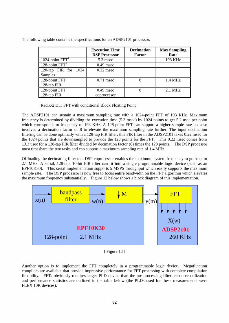
82
The following table contains the specifications for an ADSP2101 processor.
Execution Time DSP Processor
Decimation Factor
Max Sampling Rate
1024-point FFT1 5.3 msec 193 KHz 128-point FFT1 0.49 msec 128-tap FIR for 1024 Samples
0.22 msec
128-point FFT 128-tap FIR
0.71 msec 8 1.4 MHz
128-point FFT 128-tap FIR
0.49 msec coprocessor
8 2.1 MHz
1Radix-2 DIT FFT with conditional Block Floating Point The ADSP2101 can sustain a maximum sampling rate with a 1024-point FFT of 193 KHz. Maximum frequency is determined by dividing the execution time (5.3 msec) by 1024 points to get 5.2 usec per point which corresponds to frequency of 193 KHz. A 128-point FFT can support a higher sample rate but also involves a decimation factor of 8 to elevate the maximum sampling rate further. The input decimation filtering can be done optimally with a 128-tap FIR filter; this FIR filter in the ADSP2101 takes 0.22 msec for the 1024 points that are downsampled to provide the 128 points for the FFT. This 0.22 msec comes from 13.3 usec for a 128-tap FIR filter divided by decimation factor (8) times the 128 points. The DSP processor must timeshare the two tasks and can support a maximum sampling rate of 1.4 MHz. Offloading the decimating filter to a DSP coprocessor enables the maximum system frequency to go back to 2.1 MHz. A serial, 128-tap, 10-bit FIR filter can fit into a single programmable logic device (such as an EPF10K30). This serial implementation supports 5 MSPS throughput which easily supports the maximum sample rate. The DSP processor is now free to focus entire bandwidth on the FFT algorithm which elevates the maximum frequency substantially. Figure 13 below shows a block diagram of this implementation.
bandpassfilter
M FFTx(n) w(n) y(m)
X(w)EPF10K30 ADSP2101
128-point 2.1 MHz 260 KHz
[ Figure 13 ]
Another option is to implement the FFT completely in a programmable logic device. Megafunction compilers are available that provide impressive performance for FFT processing with complete compilation flexibility. FFTs obviously requires larger PLD device than the pre-processing filter; resource utilization and performance statistics are outlined in the table below (the PLDs used for these measurements were FLEX 10K devices):
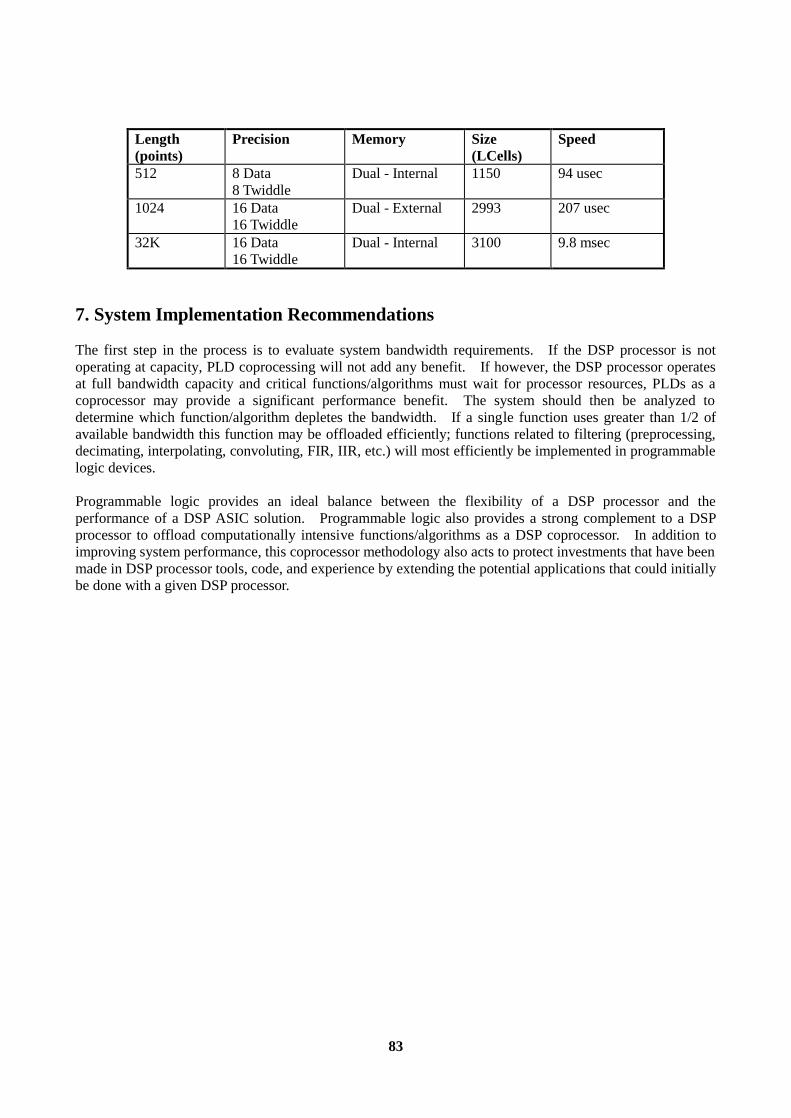
83
Length (points)
Precision Memory Size (LCells)
Speed
512 8 Data 8 Twiddle
Dual - Internal 1150 94 usec
1024 16 Data 16 Twiddle
Dual - External 2993 207 usec
32K 16 Data 16 Twiddle
Dual - Internal 3100 9.8 msec
7. System Implementation Recommendations The first step in the process is to evaluate system bandwidth requirements. If the DSP processor is not operating at capacity, PLD coprocessing will not add any benefit. If however, the DSP processor operates at full bandwidth capacity and critical functions/algorithms must wait for processor resources, PLDs as a coprocessor may provide a significant performance benefit. The system should then be analyzed to determine which function/algorithm depletes the bandwidth. If a single function uses greater than 1/2 of available bandwidth this function may be offloaded efficiently; functions related to filtering (preprocessing, decimating, interpolating, convoluting, FIR, IIR, etc.) will most efficiently be implemented in programmable logic devices. Programmable logic provides an ideal balance between the flexibility of a DSP processor and the performance of a DSP ASIC solution. Programmable logic also provides a strong complement to a DSP processor to offload computationally intensive functions/algorithms as a DSP coprocessor. In addition to improving system performance, this coprocessor methodology also acts to protect investments that have been made in DSP processor tools, code, and experience by extending the potential applications that could initially be done with a given DSP processor.
84
XI. HDTV Rate Image Processing on the Altera FLEX 10K
Doug Ridge1, Robert Hamill1, Simon Redmile2
1 - Integrated Silicon Systems Ltd., 29 Chlorine Gardens,
BELFAST, BT9 5DL, Northern Ireland. 2 - Altera UK Limited, Solar House, Globe Park, Fieldhouse Lane,
MARLOW, Buckinghamshire, SL7 1TB, England.
Abstract Image and video processing megafunctions have been developed for implementation on the Altera FLEX 10K range of CPLDs. The megafunctions, which include edge detectors, median filters, fixed and adaptive filters and DCT blocks, have been optimised for the FLEX 10K architecture to allow more functionality to be incorporated into each device. The megafunctions can operate at pixel rates of up to the HDTV standard of 54 MHz. Their size and high performance allows the CPLDs to be utilised as front-end image processing engines operating in real-time. The ability to incorporate major building blocks for image compression onto a single device also opens their use to the development of real-time imaging systems such as JPEG, MPEG and H.261.
Introduction Performing real-time image processing at pixel rates of up to the HDTV standard of 54 MHz has been an operation typically only associated with ASICs. However, the gate counts and clock rates of the Altera FLEX 10K range of CPLDs has enabled digital designers to look at these devices as flexible solutions to their image processing problems. Distributed arithmetic techniques and novel methods for function implementation, coupled with the high density and range of features on the Altera FLEX 10K range of advanced CPLDs, have enabled the development of a range of high performance front-end video and image processing functions. The functions are optimised for the Altera architecture to maximise performance whilst minimising the chip area occupied. The minimisation of the area occupied by each function enables the maximisation of the functionality which can be incorporated into the design for a single CPLD. Section 2 looks at the FLEX 10K architecture to investigate its applicability for the implementation of high performance image processing functions. This briefly covers the main structure of the architecture and new features which are being built into the devices. These will further reduce the implementation size of each image processing function, by increasing function performance, thereby allowing a reduction in the level of pipelining for each device, or allowing the use of more compact architectures. Section 3 documents the techniques used to optimise the implementation of each function for the FLEX 10K architecture and section 4 then lists the range of megafunctions which have been created for real-time image processing. As examples, a number of these megafunctions are studied in more depth to give their size and possible variants. Section 5 then draws conclusions as to the impact that these developments will have in the field of real-time image processing.
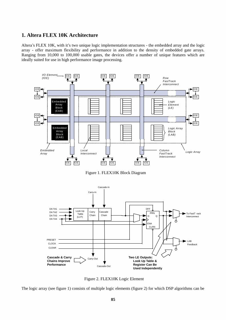
85
1. Altera FLEX 10K Architecture Altera’s FLEX 10K, with it’s two unique logic implementation structures - the embedded array and the logic array - offer maximum flexibility and performance in addition to the density of embedded gate arrays. Ranging from 10,000 to 100,000 usable gates, the devices offer a number of unique features which are ideally suited for use in high performance image processing.
IOEIOE IOEIOE
IOE
IOE
IOE
IOE
IOEIOE IOEIOE
IOE
IOE
IOE
IOE
IOEIOE
IOEIOE
EmbeddedArrayBlock(EAB)
EmbeddedArrayBlock(EAB)
LogicElement(LE)
Logic ArrayBlock(LAB)
Row FastTrackInterconnect
Logic ArrayColumn FastTrackInterconnect
LocalInterconnect
EmbeddedArray
I/O Element(IOE)
Figure 1. FLEX10K Block Diagram
rack
Feedback
DA TA1DA TA2DA TA3DA TA4
PRESETCLOCK
CLEAR
Carry-In
TInterconnect
o FastT
Carry-Out
PRN
CLRN
D Q
DFFLook-Up
Table(LUT)
CarryChain
CascadeChain
Cascade-In
Cascade-Out
LAB
ENA
Two LE Outputs: Look Up Table & Register Can Be Used Independently
Cascade & CarryChains ImprovePerformance
Figure 2. FLEX10K Logic Element The logic array (see figure 1) consists of multiple logic elements (figure 2) for which DSP algorithms can be
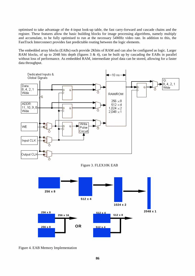
86
optimised to take advantage of the 4-input look-up table, the fast carry-forward and cascade chains and the register. These features allow the basic building blocks for image processing algorithms, namely multiply and accumulate, to be fully optimised to run at the necessary 54MHz video rate. In addition to this, the FastTrack Interconnect provides fast predictable routing between the logic elements. The embedded array blocks (EABs) each provide 2Kbits of RAM and can also be configured as logic. Larger RAM blocks, of up to 2048 bits depth (figures 3 & 4), can be built up by cascading the EABs in parallel without loss of performance. As embedded RAM, intermediate pixel data can be stored, allowing for a faster data throughput.
Figure 3. FLEX10K EAB
256 x 8
512 x 4
1024 x 2
2048 x 1256 x 8
256 x 8
512 x 4
512 x 4
256 x 16 512 x 8
OR
Figure 4. EAB Memory Implementation
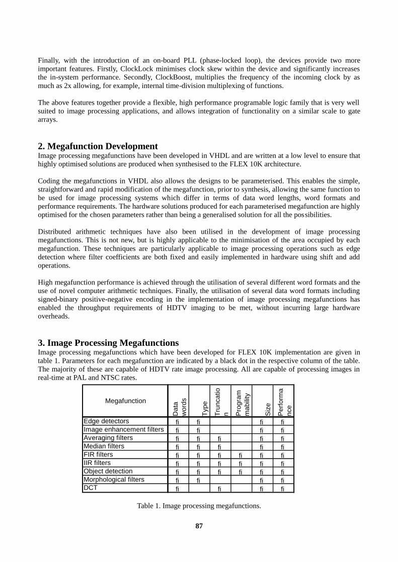
87
Finally, with the introduction of an on-board PLL (phase-locked loop), the devices provide two more important features. Firstly, ClockLock minimises clock skew within the device and significantly increases the in-system performance. Secondly, ClockBoost, multiplies the frequency of the incoming clock by as much as 2x allowing, for example, internal time-division multiplexing of functions. The above features together provide a flexible, high performance programable logic family that is very well suited to image processing applications, and allows integration of functionality on a similar scale to gate arrays. 2. Megafunction Development Image processing megafunctions have been developed in VHDL and are written at a low level to ensure that highly optimised solutions are produced when synthesised to the FLEX 10K architecture. Coding the megafunctions in VHDL also allows the designs to be parameterised. This enables the simple, straightforward and rapid modification of the megafunction, prior to synthesis, allowing the same function to be used for image processing systems which differ in terms of data word lengths, word formats and performance requirements. The hardware solutions produced for each parameterised megafunction are highly optimised for the chosen parameters rather than being a generalised solution for all the possibilities. Distributed arithmetic techniques have also been utilised in the development of image processing megafunctions. This is not new, but is highly applicable to the minimisation of the area occupied by each megafunction. These techniques are particularly applicable to image processing operations such as edge detection where filter coefficients are both fixed and easily implemented in hardware using shift and add operations. High megafunction performance is achieved through the utilisation of several different word formats and the use of novel computer arithmetic techniques. Finally, the utilisation of several data word formats including signed-binary positive-negative encoding in the implementation of image processing megafunctions has enabled the throughput requirements of HDTV imaging to be met, without incurring large hardware overheads. 3. Image Processing Megafunctions Image processing megafunctions which have been developed for FLEX 10K implementation are given in table 1. Parameters for each megafunction are indicated by a black dot in the respective column of the table. The majority of these are capable of HDTV rate image processing. All are capable of processing images in real-time at PAL and NTSC rates.
Table 1. Image processing megafunctions.
Megafunction
Dat
a w
ords
Type
Trun
catio
n Pro
gram
mab
ility
Siz
e
Per
form
anc
e
Edge detectors ® ® ® ®Image enhancement filters ® ® ® ®Averaging filters ® ® ® ® ®Median filters ® ® ® ® ®FIR filters ® ® ® ® ® ®IIR filters ® ® ® ® ® ®Object detection ® ® ® ® ® ®Morphological filters ® ® ® ®DCT ® ® ® ®

88
To illustrate the parameterised nature of the megafunctions, consider the possible variants of the Laplacian edge detector megafunction. The input data words are expected to be in an unsigned binary format. However, the word lengths of the input data words may differ from one application to the next and include, for example, 8-, 10- and 12-bit word lengths. This has been taken into consideration in the development to allow the creation of megafunctions with the specific data word lengths required by the end application. Furthermore, the pipelining parameter of the megafunction can be set to select the desired performance, whilst minimising the silicon area occupied by the megafunction implementation. A parameter to select the desired data word formats for the output has also been included. For instance, the most compact edge detection megafunction implementation has a data word which is in signed-binary positive-negative encoding format. This format is used in the megafunction architecture to achieve the high throughput rates required of HDTV rate applications. However, the designer may not wish to post-process the results when in this format. For this reason the designer can select the desired output data word format, prior to compilation.

89
Conclusions A range of parameterised image and video processing megafunctions have been developed and optimised for Altera FLEX 10K implementation. Combining many years of VLSI architectures expertise with the advanced programmable hardware of the Altera FLEX 10K family has produced megafunctions with the capability of processing images in real-time at pixel clock rates of up the HDTV standard of 54MHz. The size of the megafunctions and the gate counts of the FLEX 10K family enable multiple image processing blocks to be incorporated into the design for a single device. This allows a single device to be utilised as a high speed processing engine in support of other slower processors, or as a stand alone image processing machine. The ability to incorporate larger functional blocks such as the DCT on Altera devices and operate these in real-time opens Altera devices up for use in the real-time implementation of systems level imaging functions such as JPEG, MPEG and H.261.
90
XII. Automated Design Tools for Adaptive Filter Development
Martin Langhammer
Kaytronics, Inc.
Introduction This paper will examine methods of creating high performance adaptive filters in programmable logic. Tools for automatically generating adaptive filters will be described, along with system performance and resource requirements. Building blocks for these adaptive structures, such as multipliers and simpler filters will also be shown. 1. Filter Building Blocks The most important element of a hardware implementation of an adaptive filter is a multiplier. The feedforward stage of any adaptive filter is comprised of multipliers, as is in many cases the feedback stage. At this point, a clarification must be made on the definition of a multiplier; in some cases the multiplicative operation required for the feedback correlation in adaptive filter types such as the LMS, zero forcing, and decision directed filters may be implemented in a look up table format, rather than a multiplier structure. In these cases, the result of the multiply is often the error value, with the sign dependent on the direction to the closest symbol to the estimate. To facilitate the efficient, and automated, implementation of adaptive filters, a new signed multiplier algorithm for programmable logic was developed, and an LPM (library of parameterized modules) was written using AHDL Version 6.1 from Altera. The table below summarizes resource and performance data for several multipliers, implemented in Altera FLEX 8000 devices.
Pipelined Non- Pipelined Multiplier Size A-4 A-2 Size A-4 A-2 8 x 8 139 LC 83 MHz 106 MHz 136 LC 42.3 ns 30.0 ns 10 x 12 282 LC 66 MHz 89 Mhz 260 LC 63.3 ns 39.5 ns 16 x 16 550 LC 51 Mhz 69 Mhz 537 LC 66.5 ns 47.9 ns
Table 1: Multiplier Data Note: Performance data for the non-pipelined multipliers includes on and off chip delays. System implementation utilizing these structures will be faster, as the signal sources and destinations will be on chip, rather than off chip. As can be seen from the table, there is a predictable logarithmic relationship between word width and size, and a linear relationship between word width and performance. All multipliers in Table 1 have full output precision. Small size and speed gains may be achieved by cropping LSBs from the output, which is also automatically handled by the same multiplier LPM. Table 2 gives some examples:
91
Pipelined Multiplier Size Performance (A-2) 8 x 8, 10 bits result 132 LCs 109 Mhz 10 x 12, 14 bits 269 LCs 87 Mhz 16 x 16, 18 bits 534 LCs 70 Mhz
Table 2: Partial Output Multiplier Data
The combinatorial multipliers required for many of the correlation calculation are only one level of logic deep, and therefore will operate as fast as the pipelined multiplier in that part. The size will be approximately that of the precision of the error signal used for the correlation. 2. Filter Design and Implementation An LPM has been developed to automatically generate LMS filter structures for programmable logic. The same structure may also be used to construct decision directed filters. A large number of parameters allows the extensive specification of the filter. The feedforward section of the filter is implemented as an FIR direct form 2 filter. The correlation multipliers are instantiated with the algorithmic multipliers, except in the case when only the sign of the decision is used in the correlation, when a look up table is used. The parameters of the LPM are:
Parameter Description Range Action LPM_TAPS 3 - 32 Number of Feedforward Taps LPM_CENTER A, 1 A: Adaptive Center Tap
1: Fixed at Unity LPM_SIGIN Any Positive Integer Input Signal Precision LPM_COEFF 3 - 32 Feedforward Weight
Precision LPM_PREC Any Positive Integer Output Precision of Tap LPM_ERRW Positive Integer,
<LPM_WIDTHO Error between estimate and nearest symbol
LPM_ERRSIG Positive Integer, <LPM_SIGIN
Signal for Correlation
LPM_CONV Positive Real Number Inverse of Convergence Constant
LPM_WIDTHO Positive Integer, <(LPM_SIGIN + LPM_COEFF + ceil(log2LPM_TAPS) -1)
Precision of Estimate
Table 3: Parameters for LMS Adaptive Filter LPM
Although the filter built with this LPM follows a typical LMS filter topology, the calculation of the error, and therefore the symbol estimation, is left to the user. This will allow the designer greater flexibility in the specification of their design, as well as the ability to use the structure as a building block for more complicated designs, such as a decision feedback equalizer.
92
Fig 1: Constructing a Decision Feedback Filter In the above figure, two different LMS filters created using the LPM are used to construct a decision feedback filter. The structure of the LMS filter is shown below, in figure 2:
Fig 2: Structure of LMS Filter The convergence constant, µ, is implemented using one of two, and sometimes both, techniques. The integrators are accumulators, that have far greater precision than the output precision of the correlation multipliers and the feedforward weight precision (LPM_COEFF) combined. (The feedforward weights are taken from the most significant bits of the accumulator, while the correlation results are fed into the least significant bits of the accumulator.) The middle bits make up the bulk of the convergence multiplication, which are chosen such that they are the inverse of the nearest fractional powers of two value greater than µ. In the case where µ cannot exactly be expressed in this form, a constant multiplication (not shown in figure 2) is instantiated where the error signal enters the filter block. A very efficient constant multiplier LPM has also been developed, which allows for constant multipliers to be automatically designed, which require far
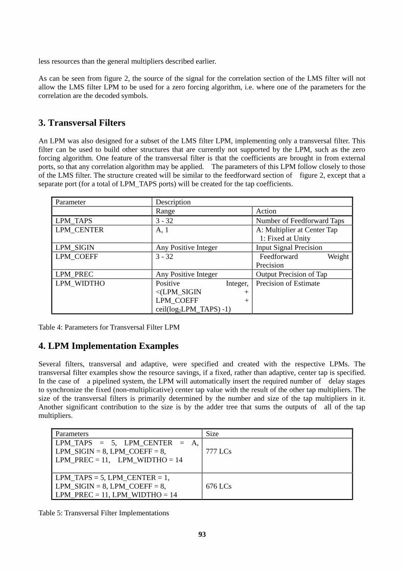
93
less resources than the general multipliers described earlier. As can be seen from figure 2, the source of the signal for the correlation section of the LMS filter will not allow the LMS filter LPM to be used for a zero forcing algorithm, i.e. where one of the parameters for the correlation are the decoded symbols. 3. Transversal Filters An LPM was also designed for a subset of the LMS filter LPM, implementing only a transversal filter. This filter can be used to build other structures that are currently not supported by the LPM, such as the zero forcing algorithm. One feature of the transversal filter is that the coefficients are brought in from external ports, so that any correlation algorithm may be applied. The parameters of this LPM follow closely to those of the LMS filter. The structure created will be similar to the feedforward section of figure 2, except that a separate port (for a total of LPM_TAPS ports) will be created for the tap coefficients.
Parameter Description Range Action LPM_TAPS 3 - 32 Number of Feedforward Taps LPM_CENTER A, 1 A: Multiplier at Center Tap
1: Fixed at Unity LPM_SIGIN Any Positive Integer Input Signal Precision LPM_COEFF 3 - 32 Feedforward Weight
Precision LPM_PREC Any Positive Integer Output Precision of Tap LPM_WIDTHO Positive Integer,
<(LPM_SIGIN + LPM_COEFF + ceil(log2LPM_TAPS) -1)
Precision of Estimate
Table 4: Parameters for Transversal Filter LPM 4. LPM Implementation Examples Several filters, transversal and adaptive, were specified and created with the respective LPMs. The transversal filter examples show the resource savings, if a fixed, rather than adaptive, center tap is specified. In the case of a pipelined system, the LPM will automatically insert the required number of delay stages to synchronize the fixed (non-multiplicative) center tap value with the result of the other tap multipliers. The size of the transversal filters is primarily determined by the number and size of the tap multipliers in it. Another significant contribution to the size is by the adder tree that sums the outputs of all of the tap multipliers.
Parameters Size LPM_TAPS = 5, LPM_CENTER = A, LPM_SIGIN = 8, LPM_COEFF = 8, LPM_PREC = 11, LPM_WIDTHO = 14
777 LCs
LPM_TAPS = 5, LPM_CENTER = 1, LPM_SIGIN = 8, LPM_COEFF = 8, LPM_PREC = 11, LPM_WIDTHO = 14
676 LCs
Table 5: Transversal Filter Implementations
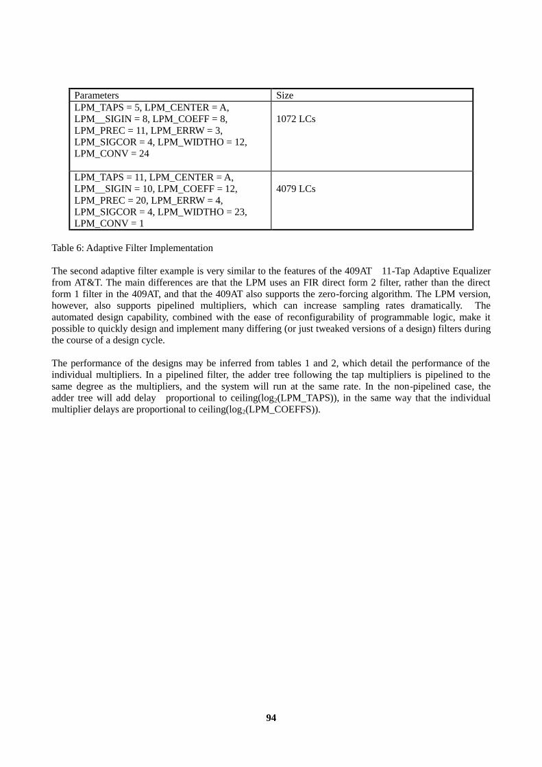
94
Parameters Size LPM_TAPS = 5, LPM_CENTER = A, LPM__SIGIN = 8, LPM_COEFF = 8, LPM_PREC = 11, LPM_ERRW = 3, LPM_SIGCOR = 4, LPM_WIDTHO = 12, LPM_CONV = 24
1072 LCs
LPM_TAPS = 11, LPM_CENTER = A, LPM__SIGIN = 10, LPM_COEFF = 12, LPM_PREC = 20, LPM_ERRW = 4, LPM_SIGCOR = 4, LPM_WIDTHO = 23, LPM_CONV = 1
4079 LCs
Table 6: Adaptive Filter Implementation The second adaptive filter example is very similar to the features of the 409AT 11-Tap Adaptive Equalizer from AT&T. The main differences are that the LPM uses an FIR direct form 2 filter, rather than the direct form 1 filter in the 409AT, and that the 409AT also supports the zero-forcing algorithm. The LPM version, however, also supports pipelined multipliers, which can increase sampling rates dramatically. The automated design capability, combined with the ease of reconfigurability of programmable logic, make it possible to quickly design and implement many differing (or just tweaked versions of a design) filters during the course of a design cycle. The performance of the designs may be inferred from tables 1 and 2, which detail the performance of the individual multipliers. In a pipelined filter, the adder tree following the tap multipliers is pipelined to the same degree as the multipliers, and the system will run at the same rate. In the non-pipelined case, the adder tree will add delay proportional to ceiling(log2(LPM_TAPS)), in the same way that the individual multiplier delays are proportional to ceiling(log2(LPM_COEFFS)).

95
Conclusions As design cycles shrink, and products increase in complexity, improved methods must be found to increase productivity as well as quality. Using automated design tools makes it more feasible to quickly design, adapt, and implement a solution, as well as reducing coding errors. System designers can now specify building blocks that are tailored to their particular needs. In this paper, automated design tools were presented that can be used for this new development environment. Several examples have been shown that can equal standard products, as well as adapting them to changing requirements. References 1. Proakis, J.G. (1989). Digital Communications, 2d ed. McGraw Hill, New York. 2. Widrow, B. and Stearns, S.D. (1985). Adaptive Signal Processing, Prentice-Hall, New Jersey. 3. “409AT - Product Data Sheet”, AT&T Microelectronics.
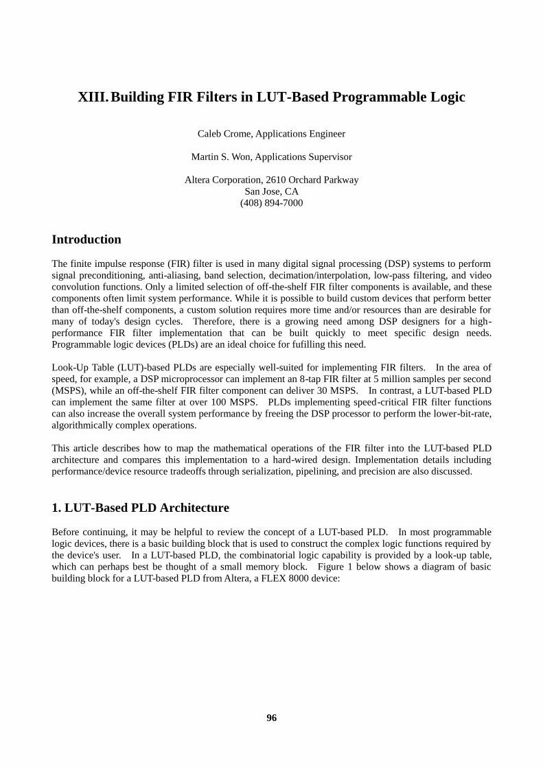
96
XIII. Building FIR Filters in LUT-Based Programmable Logic
Caleb Crome, Applications Engineer
Martin S. Won, Applications Supervisor
Altera Corporation, 2610 Orchard Parkway San Jose, CA
(408) 894-7000 Introduction
The finite impulse response (FIR) filter is used in many digital signal processing (DSP) systems to perform signal preconditioning, anti-aliasing, band selection, decimation/interpolation, low-pass filtering, and video convolution functions. Only a limited selection of off-the-shelf FIR filter components is available, and these components often limit system performance. While it is possible to build custom devices that perform better than off-the-shelf components, a custom solution requires more time and/or resources than are desirable for many of today's design cycles. Therefore, there is a growing need among DSP designers for a high-performance FIR filter implementation that can be built quickly to meet specific design needs. Programmable logic devices (PLDs) are an ideal choice for fufilling this need. Look-Up Table (LUT)-based PLDs are especially well-suited for implementing FIR filters. In the area of speed, for example, a DSP microprocessor can implement an 8-tap FIR filter at 5 million samples per second (MSPS), while an off-the-shelf FIR filter component can deliver 30 MSPS. In contrast, a LUT-based PLD can implement the same filter at over 100 MSPS. PLDs implementing speed-critical FIR filter functions can also increase the overall system performance by freeing the DSP processor to perform the lower-bit-rate, algorithmically complex operations. This article describes how to map the mathematical operations of the FIR filter into the LUT-based PLD architecture and compares this implementation to a hard-wired design. Implementation details including performance/device resource tradeoffs through serialization, pipelining, and precision are also discussed. 1. LUT-Based PLD Architecture Before continuing, it may be helpful to review the concept of a LUT-based PLD. In most programmable logic devices, there is a basic building block that is used to construct the complex logic functions required by the device's user. In a LUT-based PLD, the combinatorial logic capability is provided by a look-up table, which can perhaps best be thought of a small memory block. Figure 1 below shows a diagram of basic building block for a LUT-based PLD from Altera, a FLEX 8000 device:
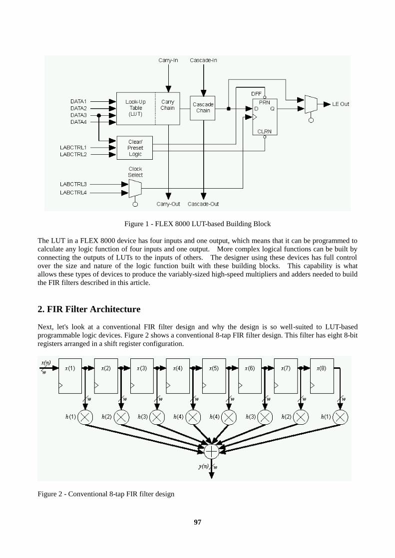
97
Figure 1 - FLEX 8000 LUT-based Building Block The LUT in a FLEX 8000 device has four inputs and one output, which means that it can be programmed to calculate any logic function of four inputs and one output. More complex logical functions can be built by connecting the outputs of LUTs to the inputs of others. The designer using these devices has full control over the size and nature of the logic function built with these building blocks. This capability is what allows these types of devices to produce the variably-sized high-speed multipliers and adders needed to build the FIR filters described in this article. 2. FIR Filter Architecture Next, let's look at a conventional FIR filter design and why the design is so well-suited to LUT-based programmable logic devices. Figure 2 shows a conventional 8-tap FIR filter design. This filter has eight 8-bit registers arranged in a shift register configuration.
Figure 2 - Conventional 8-tap FIR filter design
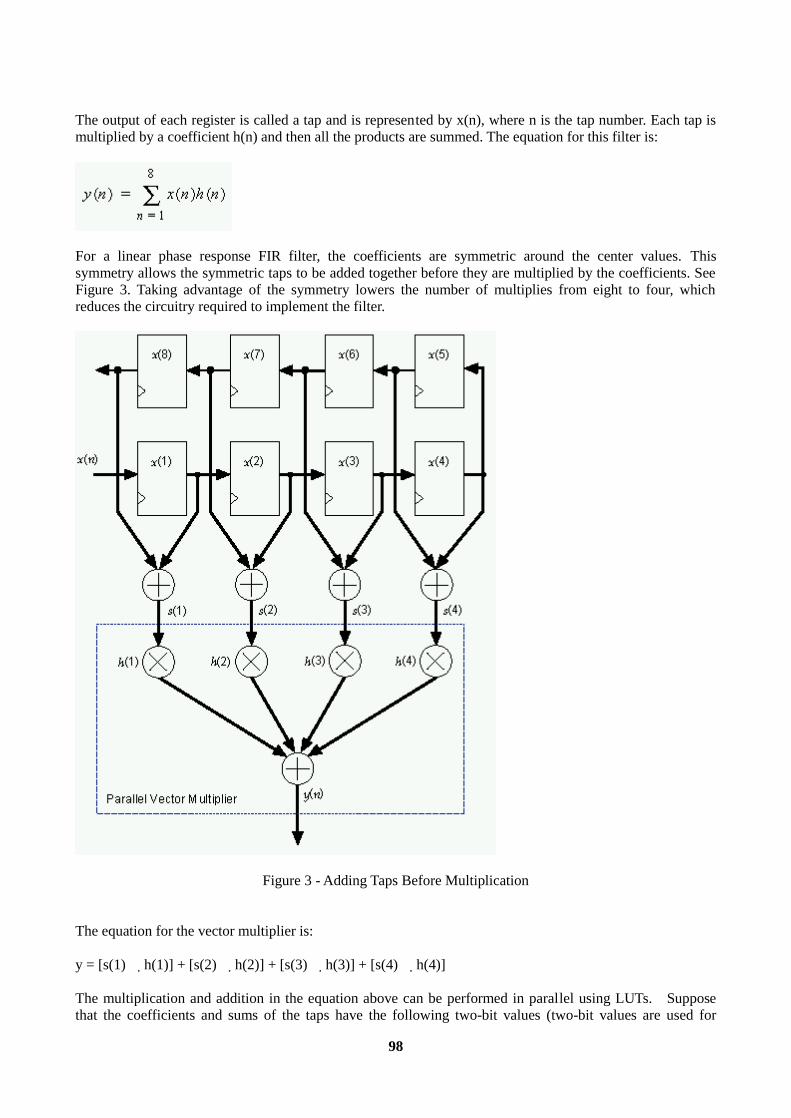
98
The output of each register is called a tap and is represented by x(n), where n is the tap number. Each tap is multiplied by a coefficient h(n) and then all the products are summed. The equation for this filter is:
For a linear phase response FIR filter, the coefficients are symmetric around the center values. This symmetry allows the symmetric taps to be added together before they are multiplied by the coefficients. See Figure 3. Taking advantage of the symmetry lowers the number of multiplies from eight to four, which reduces the circuitry required to implement the filter.
Figure 3 - Adding Taps Before Multiplication The equation for the vector multiplier is: y = [s(1) h(1)] + [s(2) h(2)] + [s(3) h(3)] + [s(4) h(4)] The multiplication and addition in the equation above can be performed in parallel using LUTs. Suppose that the coefficients and sums of the taps have the following two-bit values (two-bit values are used for

99
simplicity; the concept can be extended to larger bit widths): h(1) = 01, h(2) = 11, h(3) = 10, h(4) = 11 s(1) = 11, s(2) = 00, s(3) = 10, s(4) = 01 The multiplication and addition for the vector multiplier are shown below: Multiplicand h(n) = 01 11 10 11 Multiplier s(n) = 11 00 10 01 Partial Product P1(n) = 01 00 00 11 = 100 Partial Product P2(n) = 01 00 10 00 = 011 ____________________________________________________ Sum = 011 000 100 011 = 1010 In the multiplication above, the four digits shown in bold text are the LSBs of each s(n), and are represented by s(n)1 . Each partial product P1(n)— in italics—is either 00 or the corresponding value of the multiplicand’s h(n). The sum of all partial products P1(n) is P1 (in this case 100). Because s(n)1 for the 4 multipliers uniquely determines the value for P1, there are only 16 possible values for P1. The table below lists all possible values for P1 based on s(n)1: Value of Each Partial Product (P1) for LSB value s(n)1 s(n)1 P1 Result 0000 0 00 + 00 + 00 + 00 = 0000 0001 h(1) 00 + 00 + 00 + 01 = 0001 0010 h(2) 00 + 00 + 11 + 00 = 0011 0011 h(2) + h(1) 00 + 00 + 11 + 01 = 0100 0100 h(3) 00 + 10 + 00 + 00 = 0010 0101 h(3) + h(1) 00 + 10 + 00 + 01 = 0011 0110 h(3) + h(2) 00 + 10 + 11 + 00 = 0101 0111 h(3) + h(2) + h(1) 00 + 10 + 11 + 01 = 0110 1000 h(4) 11 + 00 + 00 + 00 = 0011 1001 h(4) + h(1) 11 + 00 + 00 + 01 = 0100 1010 h(4) + h(2) 11 + 00 + 11 + 00 = 0110 1011 h(4) + h(2) + h(1) 11 + 00 + 11 + 01 = 0111 1100 h(4) + h(3) 11 + 10 + 00 + 00 = 0101 1101 h(4) + h(3) + h(1) 11 + 10 + 00 + 01 = 0110 1110 h(4) + h(3) + h(2) 11 + 10 + 11 + 00 = 1000 1111 h(4) + h(3) + h(2) + h(1) 11 + 10 + 11 + 01 = 1001 The partial product P2 can be calculated in the same manner, except the result must be shifted left by one bit (or multiplied by two in the binary domain) before adding P1 and P2. In this example, the result is four bits wide. Therefore, the adders must be four bits wide. The partial products (P1 and P2) can be calculated by eight 4-input LUTs. All computations occur in parallel. The partial products can be fed into a tree of adders to calculate the final product called y(n) as shown in Figure 4.
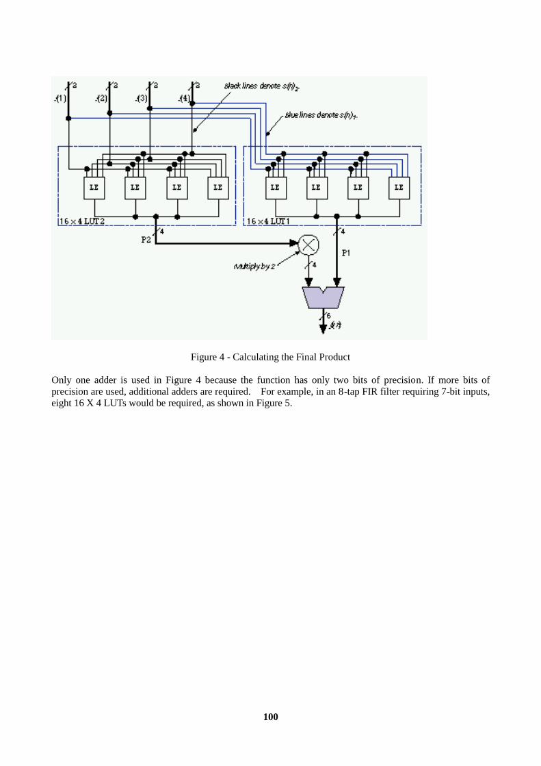
100
Figure 4 - Calculating the Final Product Only one adder is used in Figure 4 because the function has only two bits of precision. If more bits of precision are used, additional adders are required. For example, in an 8-tap FIR filter requiring 7-bit inputs, eight 16 X 4 LUTs would be required, as shown in Figure 5.
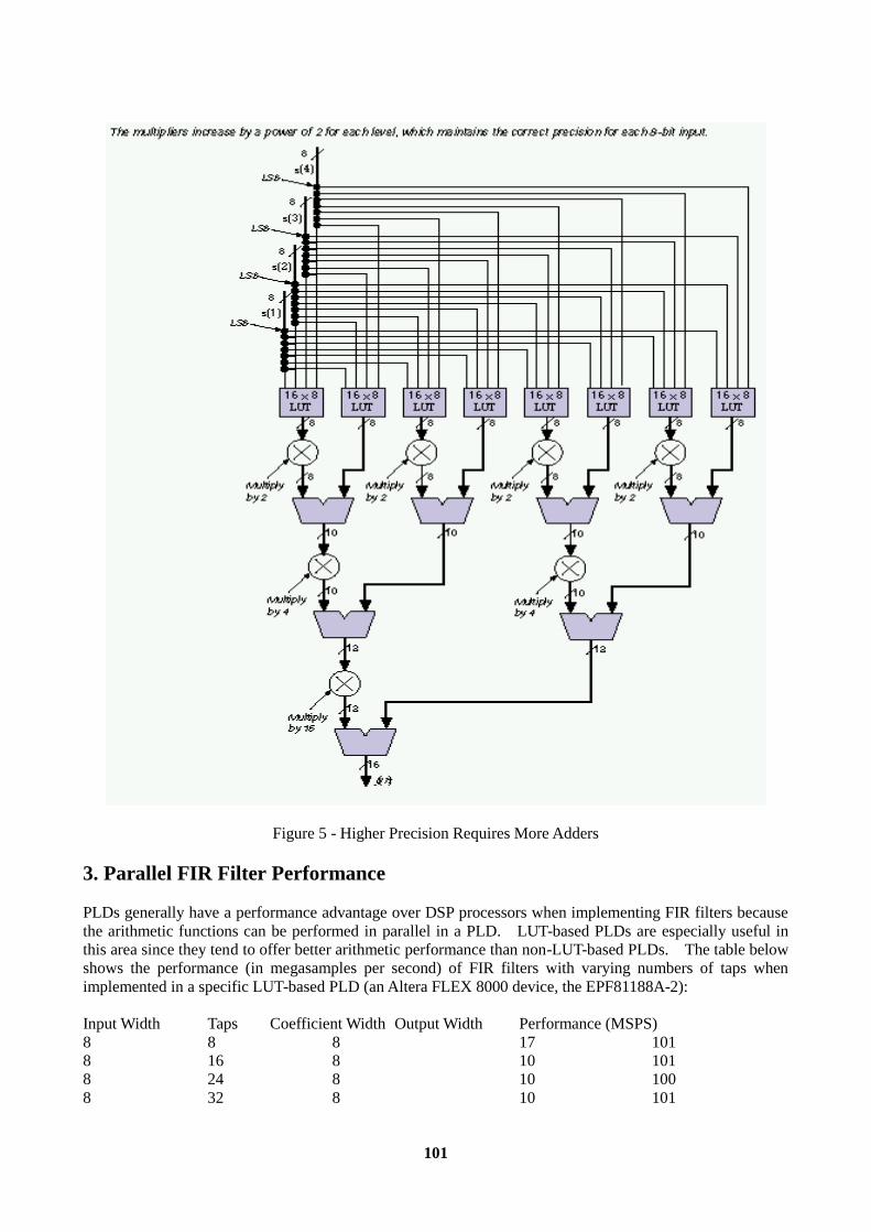
101
Figure 5 - Higher Precision Requires More Adders 3. Parallel FIR Filter Performance PLDs generally have a performance advantage over DSP processors when implementing FIR filters because the arithmetic functions can be performed in parallel in a PLD. LUT-based PLDs are especially useful in this area since they tend to offer better arithmetic performance than non-LUT-based PLDs. The table below shows the performance (in megasamples per second) of FIR filters with varying numbers of taps when implemented in a specific LUT-based PLD (an Altera FLEX 8000 device, the EPF81188A-2): Input Width Taps Coefficient Width Output Width Performance (MSPS) 8 8 8 17 101 8 16 8 10 101 8 24 8 10 100 8 32 8 10 101

102
4. Serial FIR Filters So far, we have discussed fully parallel filters (in which as many arithmetic operations are performed in parallel as possible). It is also possible to introduce serial arithmetic operation into a LUT-based PLD filter. The general tradeoff involved in introducing serialization is a reduction in the amount of device resources required to build the filter, and a corresponding reduction in the performance of the filter. Figure 6 shows a fully serial FIR filter. This architecture is similar to the fully parallel FIR filter in that it uses the LUT to store the precomputed partial products P1, P2 ... Pn, where n = <data width> + 1. The serial filter in Figure 5 performs the same computation as the parallel filter, but it only processes one bit of the input data at a time. The serial filter first computes P1, which is a function of the four bits s(1)1 through s(4)1 . On each successive cycle the serial filter computes the next partial product Pn from inputs s(1)n through s(4)n . The partial products are summed in the scaling accumulator, which divides the previous result by 2 during each clock cycle (it shifts the previous data right by one bit). This produces a final product after <data width> + 1 clock cycles because when the data passes though the symmetric tap adders (at the top of Figure 5) the data is <data width> + 1 bits wide (the fully parallel version has <data width> + 1 LUTs for the same reason). The serial FIR filter reuses the same LUT, rather than using extra circuitry.
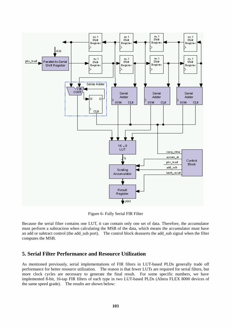
103
Figure 6- Fully Serial FIR Filter Because the serial filter contains one LUT, it can contain only one set of data. Therefore, the accumulator must perform a subtraction when calculating the MSB of the data, which means the accumulator must have an add or subtract control (the add_sub port). The control block deasserts the add_sub signal when the filter computes the MSB. 5. Serial Filter Performance and Resource Utilization As mentioned previously, serial implementations of FIR filters in LUT-based PLDs generally trade off performance for better resource utilization. The reason is that fewer LUTs are required for serial filters, but more clock cycles are necessary to generate the final result. For some specific numbers, we have implemented 8-bit, 16-tap FIR filters of each type in two LUT-based PLDs (Altera FLEX 8000 devices of the same speed grade). The results are shown below:
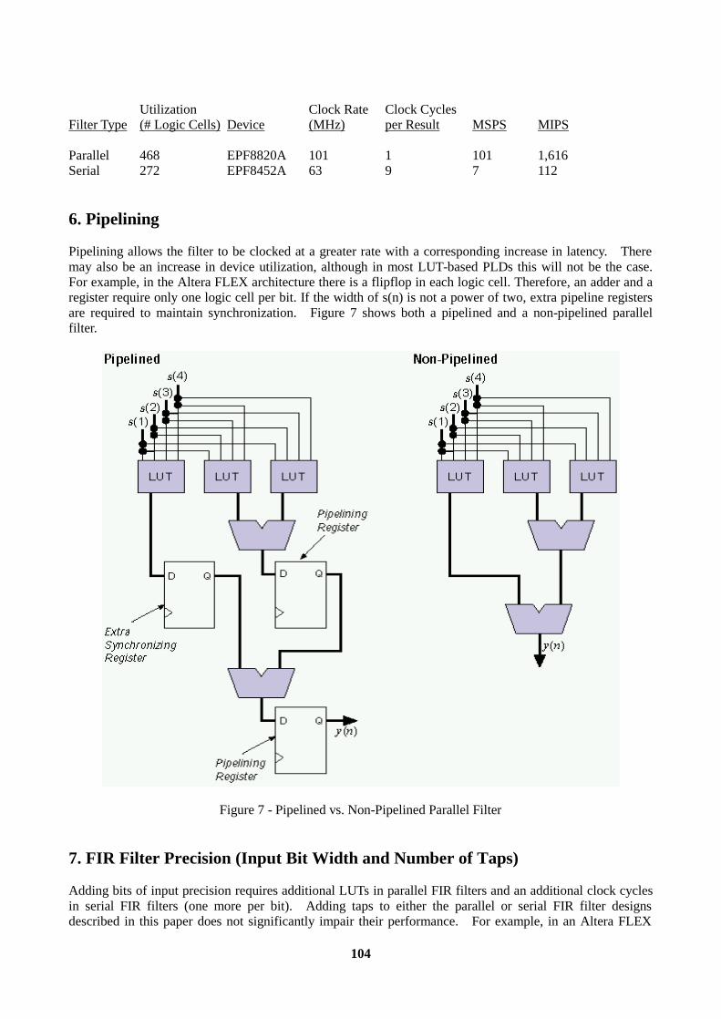
104
Utilization Clock Rate Clock Cycles Filter Type (# Logic Cells) Device (MHz) per Result MSPS MIPS Parallel 468 EPF8820A 101 1 101 1,616 Serial 272 EPF8452A 63 9 7 112 6. Pipelining Pipelining allows the filter to be clocked at a greater rate with a corresponding increase in latency. There may also be an increase in device utilization, although in most LUT-based PLDs this will not be the case. For example, in the Altera FLEX architecture there is a flipflop in each logic cell. Therefore, an adder and a register require only one logic cell per bit. If the width of s(n) is not a power of two, extra pipeline registers are required to maintain synchronization. Figure 7 shows both a pipelined and a non-pipelined parallel filter.
Figure 7 - Pipelined vs. Non-Pipelined Parallel Filter 7. FIR Filter Precision (Input Bit Width and Number of Taps) Adding bits of input precision requires additional LUTs in parallel FIR filters and an additional clock cycles in serial FIR filters (one more per bit). Adding taps to either the parallel or serial FIR filter designs described in this paper does not significantly impair their performance. For example, in an Altera FLEX
105
8000A-2 device, a pipelined 32-tap parallel FIR filter performs at the same speed as an 8-tap parallel FIR filter: 101 MSPS. 8. LUT-Based PLDs as DSP Coprocessors In any given DSP product that utilizes a DSP processor, FIR filters (and other DSP functions) can occupy large amounts of that processor's bandwidth. In many cases, it may be desirable to offload these processor-intensive functions onto less-flexible devices that are dedicated to performing them in high-speed parallel operation. LUT-based PLDs are ideal for this purpose, as the data in this article shows. In addition to implementing FIR filters, LUT-based PLDs are capable of performing any arithmetic functions that involve additive and/or multiplicative-type operations, which encompasses the majority of DSP functions. Additionally, most LUT-based PLDs are also reconfigurable in-system, which means that a single PLD can implement many DSP coprocessor functions during operation, depending on the needs of the system. Taken together, these facts clearly indicate the advantage provided by LUT-based programmable logic devices to the DSP designer.
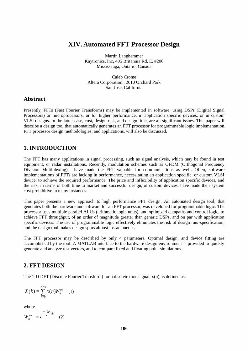
106
XIV. Automated FFT Processor Design
Martin Langhammer
Kaytronics, Inc, 405 Britannia Rd. E. #206 Mississauga, Ontario, Canada
Caleb Crome
Altera Corporation., 2610 Orchard Park San Jose, California
Abstract Presently, FFTs (Fast Fourier Transforms) may be implemented in software, using DSPs (Digital Signal Processors) or microprocessors, or for higher performance, in application specific devices, or in custom VLSI designs. In the latter case, cost, design risk, and design time, are all significant issues. This paper will describe a design tool that automatically generates an FFT processor for programmable logic implementation. FFT processor design methodologies, and applications, will also be discussed. 1. INTRODUCTION The FFT has many applications in signal processing, such as signal analysis, which may be found in test equipment, or radar installations. Recently, modulation schemes such as OFDM (Orthogonal Frequency Division Multiplexing), have made the FFT valuable for communications as well. Often, software implementations of FFTs are lacking in performance, necessitating an application specific, or custom VLSI device, to achieve the required performance. The price and inflexibility of application specific devices, and the risk, in terms of both time to market and successful design, of custom devices, have made their system cost prohibitive in many instances. This paper presents a new approach to high performance FFT design. An automated design tool, that generates both the hardware and software for an FFT processor, was developed for programmable logic. The processor uses multiple parallel ALUs (arithmetic logic units), and optimized datapaths and control logic, to achieve FFT throughput, of an order of magnitude greater than generic DSPs, and on par with application specific devices. The use of programmable logic effectively eliminates the risk of design mis-specification, and the design tool makes design spins almost instantaneous. The FFT processor may be described by only 4 parameters. Optimal design, and device fitting are accomplished by the tool. A MATLAB interface to the hardware design environment is provided to quickly generate and analyze test vectors, and to compare fixed and floating point simulations. 2. FFT DESIGN The 1-D DFT (Discrete Fourier Transform) for a discrete time signal, x(n), is defined as:
X k x n WNnk
n
N
( ) ( )==
−
∑0
1
(1)
where
W eNnk
jN
nk=
− 2π
(2)
107
The signal x(n) is complex. The DFT may be decomposed into even and odd sequences, to develop the DIF (Decimation In Frequency) form of the FFT. The even bins are then given by:
X k x n x n N Wn
N
Nnk( ) ( ) ( )2
20
21
2
= + +
=
−
∑ (3)
and the odd bins by:
X k x n x n N Wn
N
Nk n( ) ( ) ( ) ( )2 1
20
21
2
1+ = − +
=
−
−∑ (4)
This process can be repeated until N = 2, where X(0) = x(0) + x(1), X(1) = x(0) - x(1). 3. FFT PARAMETERS
The FFT processor is described completely by 4, with an optional 5th, parameter.
PARAMETER RANGE DESCRIPTION FFT_LENGTH Any Power of 2 Length of FFT (Complex Points) DATA_WIDTH Any Positive Number Input and Output Precision TWIDDLE_WIDTH Any Positive Number Twiddle Precision MEMORY_ARCH 1, 2, 4 Number of Data Banks SUB_BINS (Optional) Any Number or Range, 0 to
FFT_LENGTH Defines Set of Output Bins (< FFT_LENGTH)
TABLE I: FFT MACRO PARAMETERS
The FFT length may be any power of two. Data and twiddle widths may be described independently. The MEMORY_ARCH parameter defines the number of separate data memory banks (the twiddle memory is automatically constructed by the tool) which is in direct proportion to the processor throughput. The SUB_BINS parameter is optional, and can be used when not all of the output bins are required. This may decrease the time the processor requires to compute the FFT, but may also increase the size of the processor. 4. FFT PROCESSOR ARCHITECTURE
The core consists of a radix 2, DIF engine, with Block Floating Point representation, which is applied once per pass during the log2(FFT_LENGTH) passes. The Block Floating Point section looks right four positions, which is greater than the maximum word growth per section; therefore incoming data may be scaled automatically to take advantage of the full precision offered by the processor.
A. Processor Core
108
The core takes advantage of a new, efficient multiplier architecture developed for programmable logic, which is available in MAXPLUS2 V6.2 and later, from Altera Corporation. The multipliers are fully parameterizable, and offer high performance with relatively modest resource requirements. Multiplier throughput, in Altera 10K-3 CPLDs ranges from 125 MHz, for 8x8 multipliers, to 79 MHz, for 16x16 multipliers. FIGURE I: FFT PROCESSOR ARCHITECTURE
B. Data RAM Banks The Data RAM may be internal or external to the programmable logic device. The number of datapaths for the FFT data will be dependent on the number of Data RAM banks. C. Control Machine and Programming For all bins out processing, a hardwired control is used for the FFT processor. The algorithm for generating the hardwired control machine takes advantage of the scaleable nature of the DIF FFT, and as a result, has a
relatively constant size, largely independent of the FFT_LENGTH parameter. This allows the user to specify a wide range of FFT lengths, with similar part utilization’s, and predictable system performance. In the case of a single memory bank, the FFT style is in-place, but constant geometry addressing is used when 2 or 4 memory banks are available. For Sub Bin processing, a microprogrammed controller is implemented, with the program flow stored in an EAB (embedded array block), on chip. 5. FFT IMPLEMENTATION The FFT processor was optimized for use with Altera 10K programmable logic devices, which contain EABs, which may be configured as 256x8 synchronous RAM blocks. Depending on data widths, and memory architecture desired, FFTs in the range of 256 to 512 points, can be implemented with on board memory resources. Tables II and III show resource and memory requirements for FFTs utilizing internal, and external memory, respectively.
Length Precision Memory Size Performance 512 16 / 8 Single 2000 LCs 186 us 512 8 / 8 Dual 1150 LCs 94 us 512 12 / 12 Dual 1970 LCs 94 us 512 16 / 16 Single 2993 LCs 190 us
TABLE II: FFT PROCESSORS (INTERNAL RAM)
109
Length Precision Memory Size Performance 1024 16/16 Single 2993 LCs 411 us 1024 16/16 Dual 2993 LCs 207 us 32768 16/16 Dual 3100 LCs 9.8 ms
TABLE III: FFT PROCESSORS (EXTERNAL RAM) - PRELIMINARY
6. FFT DESIGN CONSIDERATIONS Many approaches to the design of the FFT processor tool were considered, before settling on the current architecture. 6.1 Prime FFT Decomposition At first glance, a relatively prime radix decomposition of the FFT would be easily mapped to programmable logic, as the matrix multiplications required for short prime DFTs could easily be decoded into the LUTs (look up tables), such as used by fixed coefficient FIR filters. This was found to be impractical for a monolithic FFT processor solution. A library of DFTs would be required, all existing on the chip at the same time. In addition, a generic butterfly core would still be needed, when the FFT could no longer be decomposed into relatively prime sub-sections. The synchronization of the differing latencies of the DFTs and smaller FFTs would not allow a hardwired control machine, making the size of the FFT processor unpredictable. This method of decomposition still may be used for high performance FFT systems, using multiple FFT processors, as discussed in section VIII. 6.2 CORDIC FFT Core The CORDIC (COordinate Rotation DIgital Computer) method of complex rotations can also be used to calculate the DFT, as discussed in [4], [5], and [6]. The i-th iteration of the CORDIC algorithm is defined as: xr xr xii i i i i+ = +1 ∂ θ (5) for the real value, and for the imaginary value: xi xi xri i i i i+ = +1 ∂ θ (6) The ∂ i term is either +1, or -1, and the θ i term is a 2-i scaling factor. The CORDIC method, however, exhibits some drawbacks, such as a scaling (approximately 1.6 for useful FFT precisions), which must be accounted for. As the CORDIC algorithm is sequential in nature, with each iteration of the real and imaginary calculation - depending on the previous imaginary and real iteration - respectively, the latency through a CORDIC processor will grow linearly with increasing bit width. In addition, this will not allow efficient pruning of the output bits, as the entire precision must be kept throughout the computation, to allow the contribution of each iteration to ripple through the next stage of the algorithm. A common misconception [6] regarding programmable logic is that multipliers cannot be efficiently implemented, and the CORDIC processor will be significantly smaller.
110
During the design of the FFT processor presented here, a parallel (one complex result per clock) CORDIC core was implemented in the Altera 10K CPLDs. To achieve a throughput on the same order as the parallel multipliers, the extra delay stage that was required to match the (possible) negation in the second term of each iteration, caused the CORDIC core to be as large as the parallel complex multiplier. 6.3 Higher Radix By decomposing the DFT into a larger number of sequences, a higher radix FFT may be developed. It has been shown that a higher radix FFTs require fewer complex multiplications. [1] This can be verified by inspection of a DFT matrix, where the first column contains no multiplies. For a radix R, FFT, each butterfly will require R-1 complex multiplies, which will approach unity as a ratio of total operations in the butterfly, as R increases. The number of stages, however, at logR(FFT_LENGTH), decreases with increasing R, so that the overall number of complex operations is less. The structure of a higher radix core becomes more complex with larger R, as well. A complex twiddle must still be performed for R-1 of the butterfly results, requiring R-1 twiddle sections to take advantage of the full bandwidth available through the DFT core. This would grow prohibitively large very quickly. Higher radix FFTs are also less flexible in possible choices of FFT length, which must be in powers of R only. 7. IFFT PROCESSING The IFFT may be easily derived from the FFT. As the FFT processor is implemented in programmable logic, the user may easily add the required logic to accomplish both functions in one device. The FFT is closely related to the IFFT:
X k x n W x kN
X n Wn
N
Nnk
n
N
Nnk( ) ( ) ( ) ( )= ⇔ =
=
−
=
−−∑ ∑
0
1
0
11 (7)
The scaling of the IFFT, for a radix 2 system can be easily done by a right shift. The change in sign of the exponent, can most easily be achieved by the swapping of the real and imaginary components for both the frequency and time samples. The IFFT function can therefore be added to the FFT processor with two sets of muxes. 8. HIGHER PERFORMANCE FFTs
The prime decomposition of FFTs can be used to create a higher performance FFT system, using multiple smaller FFTs and DFTs in parallel. The derivation of the FFT from the DFT is accomplished by matrix decomposition of the DFT. In the more general case, matrix decomposition of the FFT can be defined using index maps for the time and frequency indexes. The time index map is: n K n K n= +( )1 1 2 2 (8) and the frequency index map:

111
k K k K k= +( )3 1 4 2 (9) Substituting into the definition of the DFT (1), this gives:
( )
X K k K k
x Kn K n W W W Wn
N
n
N
NK K nk
NK K n k
NK K nk
NK K n k
( )3 1 4 2
0
1
0
1
1 1 2 22
2
1
11 3 1 2 2 3 2 1 1 4 1 2 2 4 2 2
+ =
+=
−
=
−
∑ ∑
(10) When N=N1N2, with K1=N2, K4=N1, and K2,K3 = 1, this reduces to:
X k N k x N n n W W Wn
N
n
N
Nn k
Nn k
Nn k( ) ( )1 1 2
0
1
0
1
2 1 22
2
1
1
1
1 1 2 1
2
2 2+ = +=
−
=
−
∑ ∑ (11)
which in turn describes the derivation of the radix 2 FFT, when N2 or N1 = 2. This result can be used to speed up an FFT system. In the case of length 2 DFTs, the DFTs can be used on the time domain samples (spaced at N/2), the twiddle factor WN
n k2 1 applied, and then two separate N/2 FFTs applied to the upper and lower butterfly result vectors. Note that for this system speed of 2, more than twice the hardware was required. This is to be expected, as the complexity of the FFT varies as N logRadixN. This same technique can be used for any composite valued FFT system, such as a 4 length DFT by radix 2 FFTs. In certain cases, where the time and frequency maps are both modulo N, as well as being modulo 0 of each other, and providing a one to one mapping between themselves, the middle twiddle term in (11) will reduce to unity. This will only occur if the decomposition of the FFT system is into a number of matrixes which are relatively prime to, i.e. share no common factors with, the dimensions of those matrixes. One of the difficult aspects of dealing with this decomposition is finding a valid relatively prime system, and then unscrambling the frequency bins after the FFT computation has finished.
112
CONCLUSIONS A solution for the automated design of a high performance FFT processor was presented. Fully parameterizable, this tool will allow systems designers to more easily integrate FFT functions into their projects. A variety of processor performance levels may be selected, and several techniques to greatly increase the overall throughput of an FFT system, by using multiple FFT processors in parallel, were also discussed. The radix 2 approach to FFT processor was decided on after careful evaluation of many techniques. The flexibility of this method, coupled with the further possibilities of FFT system design presented, will enable the application of the FFT to a wide variety of signal processing systems. REFERENCES
1. Rabiner, L.R. and Gold, B. (1975). Theory and Application of Digital Signal Processing, Prentice Hall,
New Jersey. 2. Peled, A. and Bede, L. (1976). Digital Signal Processing, Robert E. Krieger Pub. Co. (reprint) 3. Langhammer, M. “DSP Implementation in Programmable Logic”, in Proceedings of the IEEE ASIC
Conference, in press. 4. Despain, A.M., “Very Fast Fourier Transform Algorithms Hardware for Implementation”, IEEE
Transactions on Computers, vol. C-28, May 1979. 5. Jones, K.J., “Bit Serial CORDIC DFT Computation with Multidimensional Systolic Processor Arrays”,
IEEE Journal of Oceanic Engineering, vol. 18, October 1993 6. Dick, C., “Computing the Discrete Fourier Transform on FPGA Based Systolic Arrays”, Proceedings of
FPGA ‘96 7. Altera Corporation, FLEX 10K - Embedded Programmable Logic Family - Data Sheet, 1995.
113
XV. Implementing an ATM Switch Using Megafunctions Optimized
for Programmable Logic
Bill Banzhof Member of the Technical Staff
Logic Innovations and
David Greenfield Marketing Manager, Target Applications
Altera Corporation Efficient use of megafunctions -- pre-created designs that are easily integrated into a system-level chip -- enables system designers to focus resources on developing system features that provide competitive differentiation. ASICs can be prototyped in programmable logic get the product debug cycle started sooner and enable product modifications to be implemented more easily. Dropping megafunctions into programmable logic devices (PLDs) accelerates the design cycle because designers do not spend time and resources developing these reusable blocks. These time-saving advantages are particularly important when working with complex designs. An ATM switch design provides a useful example of how the design process is enhanced using megafunctions and PLDs. Purchasing off-the-shelf megafunctions reduces time spent on designing the switch fabric and enables switch software debug to occur earlier in the design cycle. For instance, critical design elements such as operating in multicast mode, optimizing the Available Bit Rate (ABR) data path, and enhancing the system prioritization scheme are all included in the ATM layer megafunction.
Megafunction implementation can eliminate 1000 hours from the design cycle as indicated in Figure 1 & Table 1, which compares a traditional ASIC ATM design flow with a megafunction programmable logic design flow. These megafunctions also optimize performance because data transfer rates are tested and verified to ensure the switch operates as specified. In addition, the PLD implementation reduces the risk of ASIC prototype failure by enabling rapid design and system level testing. This flow still allows for future cost reduction through an ASIC migration path.
1. ATM Background Figure 2 provides details on the five basic ATM switch functions. In the physical medium dependent layer, circuitry converts weak analog signals in twisted pair wire or fiber optic cable into digital signals. Clock recovery circuits like phase-locked-loops and analog buffering generally comprise this layer. The transmission convergence layer, in receive mode, builds ATM cells from the raw data presented by the physical medium dependent layer. When transmitting, the ATM cells are converted into data streams formatted to drive the physical medium dependent layer. The call sequencing and rate coupling functions are also performed in this layer. The ATM layer is responsible for switching decisions, for updating the ATM cell header, and for providing cell sequencing and rate coupling to interface with the communications bus. The protocol microcontroller orchestrates power-on-initialization, ATM connection protocols, and permanent virtual channels. Since no “real time” data flows through this microcontroller, the performance level requirement is minimal. Management information block- counters, which keep track of the number of cells received, transmitted and mis-routed, are positioned throughout the switch. This information enables the
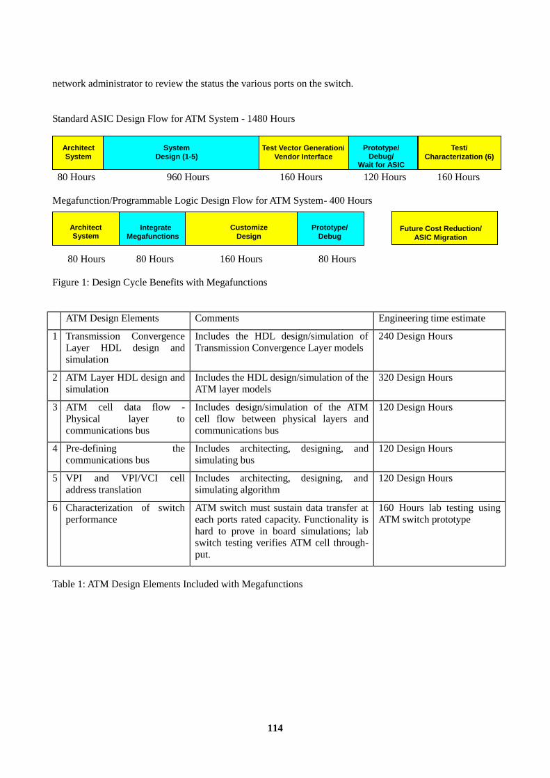
114
network administrator to review the status the various ports on the switch. Standard ASIC Design Flow for ATM System - 1480 Hours 80 Hours 960 Hours 160 Hours 120 Hours 160 Hours Megafunction/Programmable Logic Design Flow for ATM System- 400 Hours 80 Hours 80 Hours 160 Hours 80 Hours Figure 1: Design Cycle Benefits with Megafunctions ATM Design Elements Comments Engineering time estimate
1 Transmission Convergence Layer HDL design and simulation
Includes the HDL design/simulation of Transmission Convergence Layer models
240 Design Hours
2 ATM Layer HDL design and simulation
Includes the HDL design/simulation of the ATM layer models
320 Design Hours
3 ATM cell data flow - Physical layer to communications bus
Includes design/simulation of the ATM cell flow between physical layers and communications bus
120 Design Hours
4 Pre-defining the communications bus
Includes architecting, designing, and simulating bus
120 Design Hours
5 VPI and VPI/VCI cell address translation
Includes architecting, designing, and simulating algorithm
120 Design Hours
6 Characterization of switch performance
ATM switch must sustain data transfer at each ports rated capacity. Functionality is hard to prove in board simulations; lab switch testing verifies ATM cell through-put.
160 Hours lab testing using ATM switch prototype
Table 1: ATM Design Elements Included with Megafunctions
Architect System
System Design (1-5)
Architect System
Integrate Megafunctions
Test Vector Generation/ Vendor Interface
Prototype/ Debug
Customize Design
Prototype/ Debug/
Wait for ASIC
Test/ Characterization (6)
Future Cost Reduction/ ASIC Migration
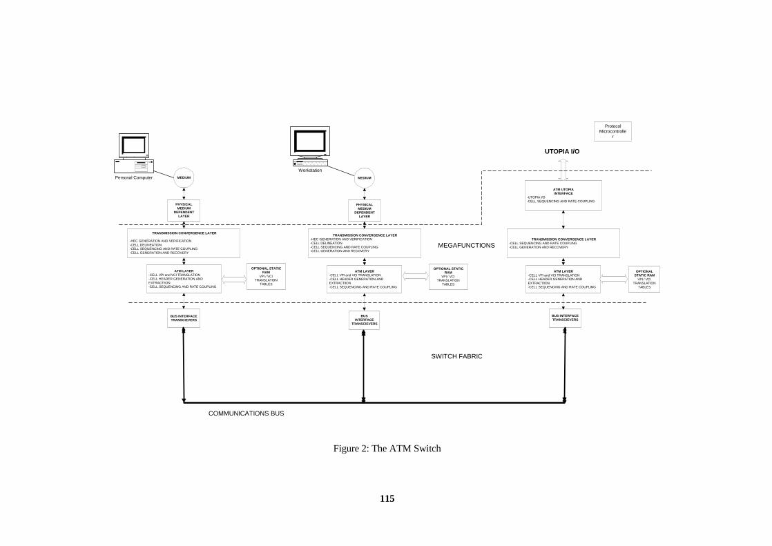
115
MEDIUM
PHYSICALMEDIUM
DEPENDENTLAYER
TRANSMISSION CONVERGENCE LAYER
-HEC GENERATION AND VERIFICATION-CELL DELINEATION-CELL SEQUENCING AND RATE COUPLING-CELL GENERATION AND RECOVERY
ATM LAYER-CELL VPI and VCI TRANSLATION-CELL HEADER GENERATION ANDEXTRACTIION-CELL SEQUENCING AND RATE COUPLING
OPTIONAL STATICRAM
VPI / VCITRANSLATION
TABLES
BUS INTERFACETRANSCIEVERS
MEDIUM
PHYSICALMEDIUM
DEPENDENTLAYER
TRANSMISSION CONVERGENCE LAYER-HEC GENERATION AND VERIFICATION-CELL DELINEATION-CELL SEQUENCING AND RATE COUPLING-CELL GENERATION AND RECOVERY
ATM LAYER-CELL VPI and VCI TRANSLATION-CELL HEADER GENERATION ANDEXTRACTIION-CELL SEQUENCING AND RATE COUPLING
OPTIONAL STATICRAM
VPI / VCITRANSLATION
TABLES
BUSINTERFACE
TRANSCIEVERS
TRANSMISSION CONVERGENCE LAYER-CELL SEQUENCING AND RATE COUPLING-CELL GENERATION AND RECOVERY
ATM LAYER-CELL VPI and VCI TRANSLATION-CELL HEADER GENERATION ANDEXTRACTIION-CELL SEQUENCING AND RATE COUPLING
OPTIONALSTATIC RAM
VPI / VCITRANSLATION
TABLES
ATM UTOPIAINTERFACE
-UTOPIA I/O-CELL SEQUENCING AND RATE COUPLING
BUS INTERFACETRANSCIEVERS
UTOPIA I/O
SWITCH FABRIC
MEGAFUNCTIONS
Personal ComputerWorkstation
COMMUNICATIONS BUS
ProtocolMicrocontrolle
r
Figure 2: The ATM Switch
116
2. ATM Megafunction Blocks Megafunctions can be used effectively when designing the transmission convergence and ATM layers because these blocks are becoming industry standard functions. The transmission convergence layer megafunctions implement serial cell inlet blocks, including ATM cell delineation and header error checking (HEC), and serial-to-parallel conversion. ATM cell delineation is performed by sampling the serial bit stream, calculating a header check sequence, and then comparing the calculated check bits against the received data. When a match is detected, the cell boundary in the serial data stream can be determined. Parallel cell inlet blocks allow the switch core logic to connect to industry standard physical layer devices using the universal test and operations physical interface (UTOPIA) interface. Binary counters include a cell header bit counter, a byte counter, and a 53-byte ATM cell counter. Other megafunction elements include the cell acceptance state machine, the cell inlet and outlet FIFOs, and serial ATM cell outlet blocks encompassing HEC field generation and parallel-to-serial conversion. The parallel ATM cell outlet blocks, which feed physical layer (PHY) devices over the UTOPIA interface, and management information block counters, are also included in the transmission convergence layer megafunction. In the ATM layer, megafunction elements include ATM cell virtual path indicator (VPI) and virtual channel indicator (VCI) address-translation-logic, and the VPI and VPI/VCI address-jamming-multiplexor. A communications bus interface -- which acts like a small but very fast local area network -- is needed along with adjacent communications bus inlet and outlet FIFOs. Additional blocks include the constant bit rate (CBR), variable bit rate (VBR), and available bit rate (ABR) data paths and priority logic. 3. Utilization of Embedded Array Blocks ATM megafunctions require efficient memory for optimized performance. One means of implementing the memory is the dedicated embedded array block (EAB) structure of Altera’s FLEX 10K architecture. Each EAB provides 2,048 bits which can be used to create RAM, ROM, FIFO functions or dual-port RAM. Maximizing the use of these EABs frees traditional logic elements, such as look-up tables (LUTs), registers, and routing resources, for non-memory logic. Access to the memory is supported in HDLs through the use of industry standard constructs like LPM and via Altera provided memory compilers for tools that do not support LPM. Sequencers can then be designed to handle complex tasks by combining the EAB with traditional logic elements. One EAB function is the storage of ATM cells between the PHY layer devices and the ATM layer logic, and between the ATM layer logic and the switch fabric. The EAB also provides the address space for implementing the VPI and VCI cell address translation. The EAB also is used ito provide limited address translation memory space in certain switch applications. This eliminates the additional cost and board space associated with adding external SRAM. Another application of the EAB is in the command and status coupling between the external protocol microcontroller and the command/status engine residing in the PLD. The EAB is used as a buffer, allowing the generation and execution of command and status packets to be performed independently of the data transfer of the packets. The command EAB is used as storage for the microcontroller as it assembles command packets. When assembled, a signal is sent to the command/status engine in the PLD indicating that a command is ready to be parsed. The microcontroller is then free to perform other processing tasks while the command/status engine is executing the command. In the reverse path, the microcontroller is not interrupted until a complete status packet has been assembled and is ready for transmission out of the status EAB.
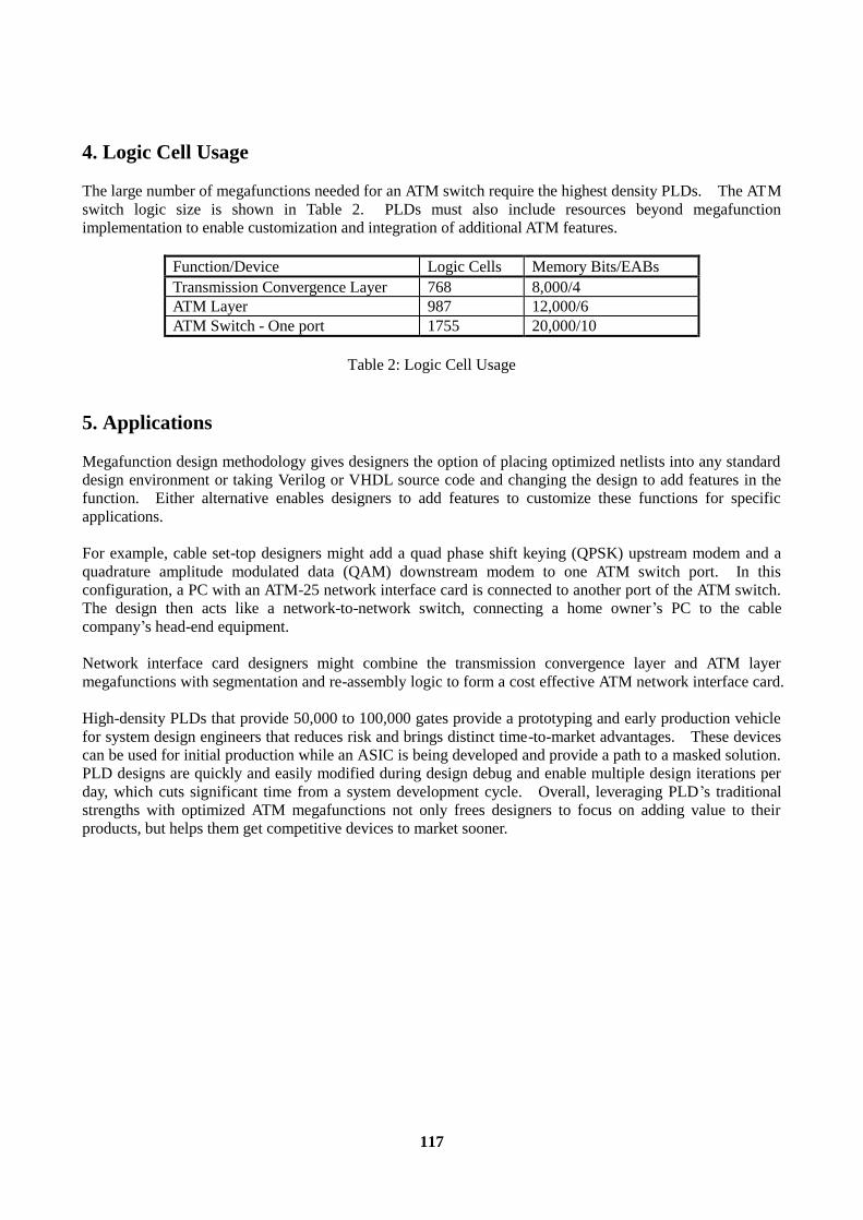
117
4. Logic Cell Usage The large number of megafunctions needed for an ATM switch require the highest density PLDs. The ATM switch logic size is shown in Table 2. PLDs must also include resources beyond megafunction implementation to enable customization and integration of additional ATM features.
Function/Device Logic Cells Memory Bits/EABs Transmission Convergence Layer 768 8,000/4 ATM Layer 987 12,000/6 ATM Switch - One port 1755 20,000/10
Table 2: Logic Cell Usage
5. Applications Megafunction design methodology gives designers the option of placing optimized netlists into any standard design environment or taking Verilog or VHDL source code and changing the design to add features in the function. Either alternative enables designers to add features to customize these functions for specific applications. For example, cable set-top designers might add a quad phase shift keying (QPSK) upstream modem and a quadrature amplitude modulated data (QAM) downstream modem to one ATM switch port. In this configuration, a PC with an ATM-25 network interface card is connected to another port of the ATM switch. The design then acts like a network-to-network switch, connecting a home owner’s PC to the cable company’s head-end equipment. Network interface card designers might combine the transmission convergence layer and ATM layer megafunctions with segmentation and re-assembly logic to form a cost effective ATM network interface card. High-density PLDs that provide 50,000 to 100,000 gates provide a prototyping and early production vehicle for system design engineers that reduces risk and brings distinct time-to-market advantages. These devices can be used for initial production while an ASIC is being developed and provide a path to a masked solution. PLD designs are quickly and easily modified during design debug and enable multiple design iterations per day, which cuts significant time from a system development cycle. Overall, leveraging PLD’s traditional strengths with optimized ATM megafunctions not only frees designers to focus on adding value to their products, but helps them get competitive devices to market sooner.
118
XVI. Incorporating Phase-Locked Loop Technology into
Programmable Logic Devices
Greg Steinke Supervisor-Component Applications
Altera Corporation, 101 Innovation Drive San Jose, CA 95134
As higher density programmable logic devices (PLDs) become available, on-chip clock distribution becomes more important to the integrity and performance of the designs implemented in these devices. The impact of clock skew and delay becomes substantial in high density PLDs, exactly as in gate array and custom chip implementations. Existing solutions for this problem, such as hardwired clock trees, are less effective for the high density PLDs that are being released in today’s programmable logic market. One recent solution to this problem is the incorporation of phase-locked loop (PLL) structures into the PLDs themselves. The PLL can then be used along with a balanced clock tree to minimize skew and delay across the device. An additional benefit of a PLL is the ability to multiply the incoming device clock. Gate array and custom chip designers have found clock multiplication very useful in their designs; a common example is in microprocessors where a 100-MHz processor may be fed by a 50-MHz clock, which is doubled in the processor. This technique allows easier board design, as the clock path on the board does not have to distribute a high-speed signal. This paper describes how to use an on-board PLL to perform these functions in Altera’s FLEX 10K and MAX 7000S devices. Specific design examples of how to reduce clock skew and perform clock multiplication are given, including schematics, VHDL and Verilog. Other considerations, such as timing and board layout considerations are also addressed. 1. ClockLock and ClockBoost Features in FLEX 10K and MAX 7000S Selected devices in the FLEX 10K and MAX 7000S device families include ClockLock and ClockBoost circuits. The devices which include ClockLock and ClockBoost are denoted with a ‘DX’ suffix in the ordering code. For instance, the EPF10K100GC503-3 does not have ClockLock circuitry, but the EPF10K100GC503-3DX does. The ClockLock and ClockBoost circuits are designed differently in the FLEX 10K and MAX 7000S families. In the FLEX 10K device family, the ClockLock circuit locks onto the incoming clock, minimizing clock delay. The ClockBoost circuit can be engaged to multiply the incoming clock by two. Whether or not the clock is multiplied, the clock delay is reduced, improving clock-to-output and setup times. In the MAX 7000S device family, the clock delay is already quite low. Therefore, the ClockLock circuitry does not further reduce clock delays. The advantage of the ClockLock circuit in MAX 7000S is the ClockBoost circuit; in MAX 7000S, the ClockBoost circuit is always engaged when ClockLock is used. The ClockBoost circuit can multiply the incoming clock by two, three, or four in MAX 7000S devices. 2. Specifying ClockLock and ClockBoost Usage in MAX+PLUS II Altera has added a new primitive to its programmable logic development system, MAX+PLUS II, to let designers take advantage of ClockLock and ClockBoost. By using the primitive CLKLOCK, a designer notifies MAX+PLUS II that the ClockLock circuitry should be used on this clock path. This is analogous to the GLOBAL primitive already used within MAX+PLUS II to tell MAX+PLUS II to use the dedicated
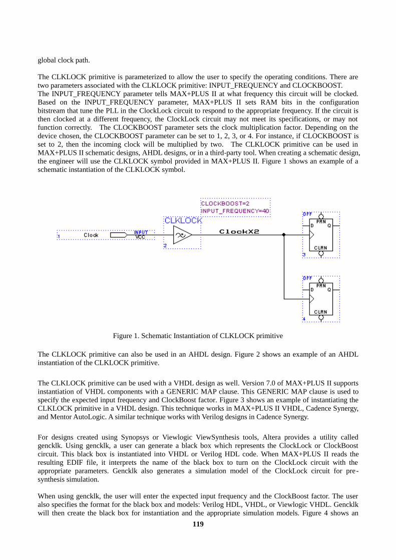
119
global clock path. The CLKLOCK primitive is parameterized to allow the user to specify the operating conditions. There are two parameters associated with the CLKLOCK primitive: INPUT_FREQUENCY and CLOCKBOOST. The INPUT_FREQUENCY parameter tells MAX+PLUS II at what frequency this circuit will be clocked. Based on the INPUT_FREQUENCY parameter, MAX+PLUS II sets RAM bits in the configuration bitstream that tune the PLL in the ClockLock circuit to respond to the appropriate frequency. If the circuit is then clocked at a different frequency, the ClockLock circuit may not meet its specifications, or may not function correctly. The CLOCKBOOST parameter sets the clock multiplication factor. Depending on the device chosen, the CLOCKBOOST parameter can be set to 1, 2, 3, or 4. For instance, if CLOCKBOOST is set to 2, then the incoming clock will be multiplied by two. The CLKLOCK primitive can be used in MAX+PLUS II schematic designs, AHDL designs, or in a third-party tool. When creating a schematic design, the engineer will use the CLKLOCK symbol provided in MAX+PLUS II. Figure 1 shows an example of a schematic instantiation of the CLKLOCK symbol.
Figure 1. Schematic Instantiation of CLKLOCK primitive
The CLKLOCK primitive can also be used in an AHDL design. Figure 2 shows an example of an AHDL instantiation of the CLKLOCK primitive. The CLKLOCK primitive can be used with a VHDL design as well. Version 7.0 of MAX+PLUS II supports instantiation of VHDL components with a GENERIC MAP clause. This GENERIC MAP clause is used to specify the expected input frequency and ClockBoost factor. Figure 3 shows an example of instantiating the CLKLOCK primitive in a VHDL design. This technique works in MAX+PLUS II VHDL, Cadence Synergy, and Mentor AutoLogic. A similar technique works with Verilog designs in Cadence Synergy. For designs created using Synopsys or Viewlogic ViewSynthesis tools, Altera provides a utility called gencklk. Using gencklk, a user can generate a black box which represents the ClockLock or ClockBoost circuit. This black box is instantiated into VHDL or Verilog HDL code. When MAX+PLUS II reads the resulting EDIF file, it interprets the name of the black box to turn on the ClockLock circuit with the appropriate parameters. Gencklk also generates a simulation model of the ClockLock circuit for pre-synthesis simulation. When using gencklk, the user will enter the expected input frequency and the ClockBoost factor. The user also specifies the format for the black box and models: Verilog HDL, VHDL, or Viewlogic VHDL. Gencklk will then create the black box for instantiation and the appropriate simulation models. Figure 4 shows an
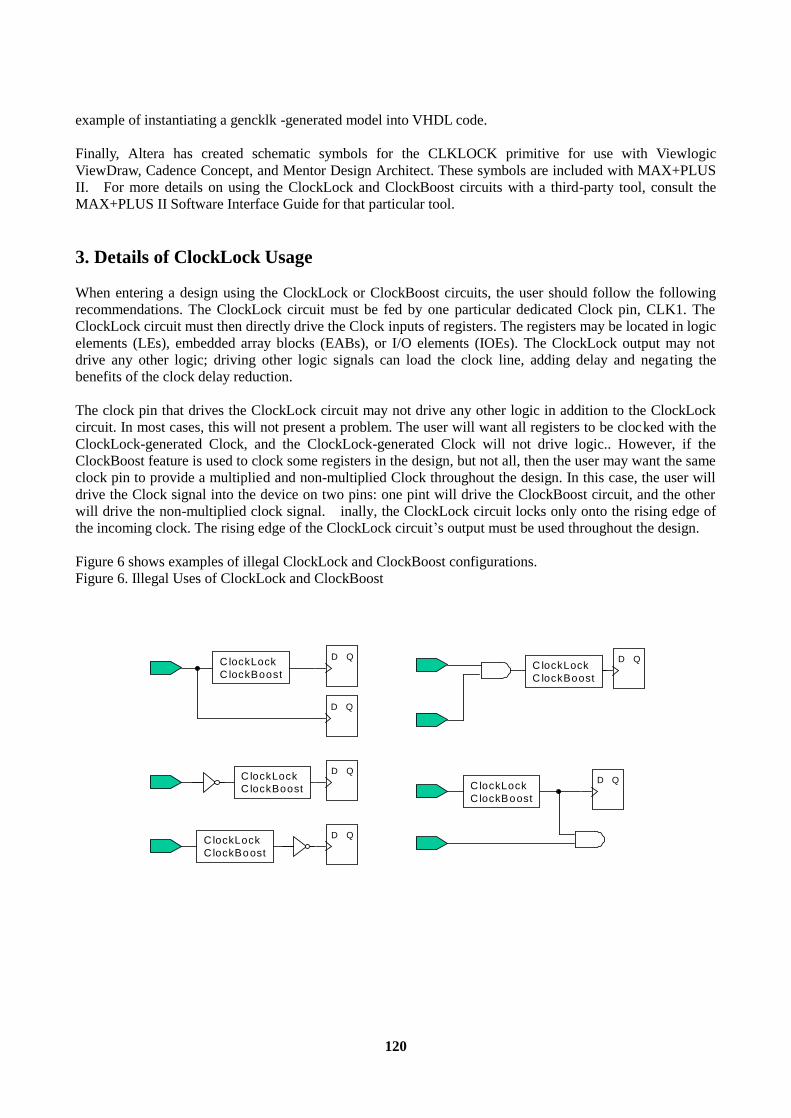
120
example of instantiating a gencklk -generated model into VHDL code. Finally, Altera has created schematic symbols for the CLKLOCK primitive for use with Viewlogic ViewDraw, Cadence Concept, and Mentor Design Architect. These symbols are included with MAX+PLUS II. For more details on using the ClockLock and ClockBoost circuits with a third-party tool, consult the MAX+PLUS II Software Interface Guide for that particular tool. 3. Details of ClockLock Usage When entering a design using the ClockLock or ClockBoost circuits, the user should follow the following recommendations. The ClockLock circuit must be fed by one particular dedicated Clock pin, CLK1. The ClockLock circuit must then directly drive the Clock inputs of registers. The registers may be located in logic elements (LEs), embedded array blocks (EABs), or I/O elements (IOEs). The ClockLock output may not drive any other logic; driving other logic signals can load the clock line, adding delay and negating the benefits of the clock delay reduction. The clock pin that drives the ClockLock circuit may not drive any other logic in addition to the ClockLock circuit. In most cases, this will not present a problem. The user will want all registers to be clocked with the ClockLock-generated Clock, and the ClockLock-generated Clock will not drive logic.. However, if the ClockBoost feature is used to clock some registers in the design, but not all, then the user may want the same clock pin to provide a multiplied and non-multiplied Clock throughout the design. In this case, the user will drive the Clock signal into the device on two pins: one pint will drive the ClockBoost circuit, and the other will drive the non-multiplied clock signal. inally, the ClockLock circuit locks only onto the rising edge of the incoming clock. The rising edge of the ClockLock circuit’s output must be used throughout the design. Figure 6 shows examples of illegal ClockLock and ClockBoost configurations. Figure 6. Illegal Uses of ClockLock and ClockBoost
D Q
D Q
C lockLockC lockBoost
D Q
D Q
D QC lockLockC lockBoost
C lockLockC lockBoost
C lockLockC lockBoost
D QC lockLockC lockBoost
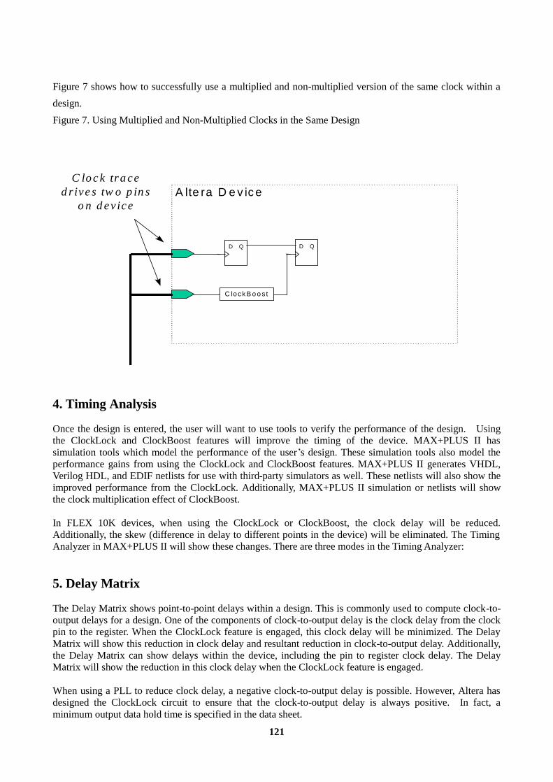
121
Figure 7 shows how to successfully use a multiplied and non-multiplied version of the same clock within a design. Figure 7. Using Multiplied and Non-Multiplied Clocks in the Same Design
D Q D Q
A lte ra D e v ic e
C lock B o o s t
C lo c k tra ced rive s tw o p in s
o n d ev ice
4. Timing Analysis Once the design is entered, the user will want to use tools to verify the performance of the design. Using the ClockLock and ClockBoost features will improve the timing of the device. MAX+PLUS II has simulation tools which model the performance of the user’s design. These simulation tools also model the performance gains from using the ClockLock and ClockBoost features. MAX+PLUS II generates VHDL, Verilog HDL, and EDIF netlists for use with third-party simulators as well. These netlists will also show the improved performance from the ClockLock. Additionally, MAX+PLUS II simulation or netlists will show the clock multiplication effect of ClockBoost. In FLEX 10K devices, when using the ClockLock or ClockBoost, the clock delay will be reduced. Additionally, the skew (difference in delay to different points in the device) will be eliminated. The Timing Analyzer in MAX+PLUS II will show these changes. There are three modes in the Timing Analyzer: 5. Delay Matrix The Delay Matrix shows point-to-point delays within a design. This is commonly used to compute clock-to-output delays for a design. One of the components of clock-to-output delay is the clock delay from the clock pin to the register. When the ClockLock feature is engaged, this clock delay will be minimized. The Delay Matrix will show this reduction in clock delay and resultant reduction in clock-to-output delay. Additionally, the Delay Matrix can show delays within the device, including the pin to register clock delay. The Delay Matrix will show the reduction in this clock delay when the ClockLock feature is engaged. When using a PLL to reduce clock delay, a negative clock-to-output delay is possible. However, Altera has designed the ClockLock circuit to ensure that the clock-to-output delay is always positive. In fact, a minimum output data hold time is specified in the data sheet.

122
6. Setup/Hold Matrix The Setup/Hold Matrix shows setup and hold times for the pins of a design. Setup times for IOE registers used as input register will improve when using the ClockLock feature, and the Setup/Hold Matrix will show this improvement. However, an input signal which is registered in an LE register will see an increase in setup time. Setup time is governed by the following equation: TSU = TDATA + TREG_SU - TCLOCK TDATA is the data delay, TREG_SU is the setup time of the register, and TCLOCK is the clock delay. The ClockLock circuit reduces clock delay. Due to the reduced clock delay, the setup time at the pin is increased. To minimize setup time when using the ClockLock circuit, the designer can use the I/O registers to register the input. 7. Registered Performance This mode of operation computes the maximum operating frequency of the design. The clock parameter that affects registered performance is skew. Without ClockLock, there is so little skew within the Logic Array and the I/O Elements that it is modeled as zero. However, there is skew between any Logic Element and any I/O Element; the clock delay to the I/O element is less than the clock delay to the LE. If the critical path in a design goes from an LE register to an IOE register, the Timing Analyzer will add the clock skew when computing registered performance. When using ClockLock, this skew will become zero. The Timing Analyzer will show this elimination of clock skew and show an improvement in registered performance. When using the ClockBoost circuit in a MAX 7000S device, clock delay is unchanged. Therefore, the Delay Matrix and Setup/Hold Matrix results will be unchanged. However, in FLEX 10K and MAX 7000S, the Registered Performance result will change. The Registered Performance analysis will report the speed of the multiplied clock; the user can divide this by the ClockBoost factor to find the maximum speed at which the pin can be clocked. If some registers in a design are clocked by the multiplied clock, and some are clocked by the non-multiplied clock, the Timing Analyzer will not compute the maximum performance of registers bridging between the multiplied and non-multiplied domains. The Timing Analzyer cannot compute this performance because it does not know the relationship between the two clocks. The user can approach this in one of two ways. One method is to use the Delay Matrix to analyze the delays between registers. Another method is to use a third-party timing analysis tool which can analyze multi-clock systems. 8. Simulation The ClockLock and ClockBoost circuits have effects on the timing and functionality of the user’s design. To accurately simulate the user’s design, the simulation tool must consider the effects of the ClockLock and ClockBoost circuits. Both the Functional Simulator and Timing Simulator in MAX+PLUS II take the effects of the ClockLock and ClockBoost circuits into account. When simulating the ClockLock and ClockBoost circuits, the MAX+PLUS II Simulator first checks that the circuits will function correctly. In order for those circuits to lock onto the incoming clock, the incoming clock must be regular and must meet the specifications stated in the datasheet. Additionally, the incoming clock frequency must match the INPUT_FREQUENCY parameter entered into MAX+PLUS II. Assuming that these conditions are met, the MAX+PLUS II Simulator will generate a clock signal which models the clock signal generated in the device. If the ClockBoost feature is used, the clock signal will be multiplied. Where appropriate, the pin-to-register clock delay will be reduced. The MAX+PLUS II simulation model acts as a silicon PLL and must sample the incoming clock before lock-

123
on. The model won’t begin to generate clocks until it has sampled three incoming clocks. Before the model locks on, it will output a logic low signal. If the incoming clock changes frequency or otherwise violates the specifications, the model will lose lock. Once lock is lost, the model will output a logic low, and will not attempt to re-acquire lock. Typically, this practice is not an issue; a designer will generally simulate with a stable clock. When performing a functional simulation in MAX+PLUS II, timing effects are ignored and all delays are assumed to be zero. When used without clock multiplication, the ClockLock circuit affects only the timing of the circuit, not the functionality. Therefore, no difference will be seen in the Functional Simulator when using only the ClockLock circuit, other than the lock-on process. However, the Functional Simulator will simulate the operation of the ClockBoost circuit, as that circuit affects the functionality of the design. A designer can simulate the operation of ClockLock and ClockBoost circuits using VHDL and Verilog simulators. To perform a pre-synthesis compilation before MAX+PLUS II compilation, a designer can use the netlist output of gencklk. During compilation, MAX+PLUS II generates VHDL and Verilog models of the ClockLock and ClockBoost circuits when they are used in the design. When used in a simulation, the models require 3 clock cycles to lock onto the incoming clock. Also, if the incoming clock changes frequency or otherwise violates the specifications, the model will lose lock. When the model is not locked, it will output a logic low. The designer can also used a gate-level simulator to simulate the operation of the ClockLock and ClockBoost circuits. A VHDL or Verilog HDL simulator can be used in conjunction with a gate-level simulator to simulate the operation of the ClockLock and ClockBoost circuits. Mentor QuickSim and Viewlogic ViewSim simulators are support via this technique. A gate-level simulator can simulate the operation of the circuit before or after MAX+PLUS II compilation. For more details on simulation in a third-party tool, consult the appropriate Software Interface Guide. 9. ClockLock Status Designers using the ClockLock circuit will want to know when the ClockLock circuit is locked onto the incoming clock; operating a design before the clock is locked may result in inconsistent operation. To support this, the ClockLock circuit has an optional LOCK output. This output is connected to one particular I/O pin on the device. When the LOCK signal is enabled, the LOCK pin will drive a logic ‘1’ when the ClockLock circuit is locked to the incoming clock, and will drive a logic ‘0’ when the ClockLock circuit loses lock. The ClockLock circuit may lose lock if the incoming clock violates the specifications for jitter or duty cycle. Lock may also be lost if the incoming clock contains glitches, becomes irregular, or stops. To monitor the LOCK signal, the user can use an option in MAX+PLUS II. The Enable LOCK Output Device Option turns on the LOCK signal. The Report File will indicate which pin is the LOCK pin. The data sheet also lists which pin is the LOCK pin on all FLEX 10K package types. The LOCK signal can then be externally monitored. For instance, an external circuit could reset the device whenever the LOCK signal goes low and then reasserts. The LOCK signal can not be internally monitored; the internal logic will experience incorrect operation once lock is lost, and must be externally controlled. FLEX devices are configured upon power-up. The ClockLock configuration information is near the beginning of the configuration data stream, so the ClockLock may lock onto the incoming clock while the rest of the device is configuring. If the system clock is applied to the CLK1 pin during configuration, the ClockLock circuit will be locked onto that clock before the FLEX 10K device finishes configuration. MAX devices begin operation as soon as VCC reaches the operating level. When using the ClockLock circuit, the user’s system should monitor the LOCK signal and reset the MAX device once the ClockLock circuit is locked to the incoming clock.
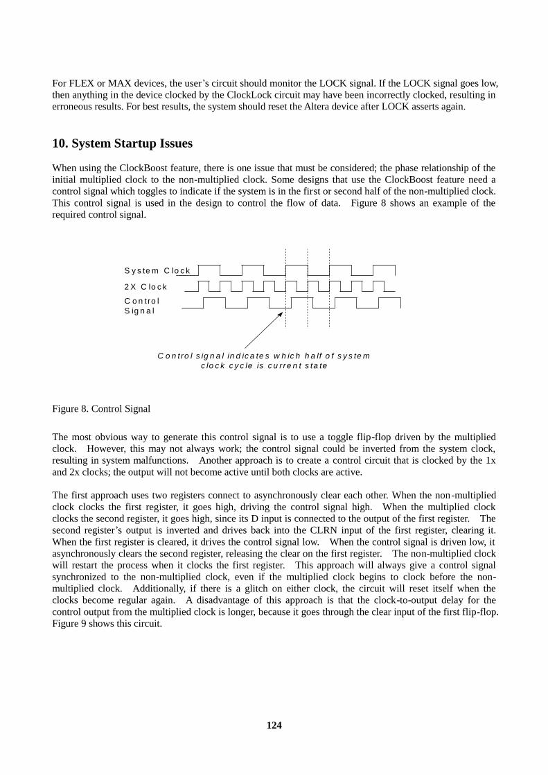
124
For FLEX or MAX devices, the user’s circuit should monitor the LOCK signal. If the LOCK signal goes low, then anything in the device clocked by the ClockLock circuit may have been incorrectly clocked, resulting in erroneous results. For best results, the system should reset the Altera device after LOCK asserts again. 10. System Startup Issues When using the ClockBoost feature, there is one issue that must be considered; the phase relationship of the initial multiplied clock to the non-multiplied clock. Some designs that use the ClockBoost feature need a control signal which toggles to indicate if the system is in the first or second half of the non-multiplied clock. This control signal is used in the design to control the flow of data. Figure 8 shows an example of the required control signal.
S y s te m C lo c k
2 X C lo c k
C o n tro lS ig n a l
C o n tro l s ig n a l in d ic a te s w h ic h h a lf o f s y s te mc lo c k c y c le is c u r re n t s ta te
Figure 8. Control Signal The most obvious way to generate this control signal is to use a toggle flip-flop driven by the multiplied clock. However, this may not always work; the control signal could be inverted from the system clock, resulting in system malfunctions. Another approach is to create a control circuit that is clocked by the 1x and 2x clocks; the output will not become active until both clocks are active. The first approach uses two registers connect to asynchronously clear each other. When the non-multiplied clock clocks the first register, it goes high, driving the control signal high. When the multiplied clock clocks the second register, it goes high, since its D input is connected to the output of the first register. The second register’s output is inverted and drives back into the CLRN input of the first register, clearing it. When the first register is cleared, it drives the control signal low. When the control signal is driven low, it asynchronously clears the second register, releasing the clear on the first register. The non-multiplied clock will restart the process when it clocks the first register. This approach will always give a control signal synchronized to the non-multiplied clock, even if the multiplied clock begins to clock before the non-multiplied clock. Additionally, if there is a glitch on either clock, the circuit will reset itself when the clocks become regular again. A disadvantage of this approach is that the clock-to-output delay for the control output from the multiplied clock is longer, because it goes through the clear input of the first flip-flop. Figure 9 shows this circuit.
125
DD
VCC
1X Clock
2X Clock
Control Signal
Figure 9. Control Signal Circuit Another approach uses a chain of registers. The first is a DFF clocked by the multiplied clock. This drives a DFF clocked by the non-multiplied act, which drives a TFF clocked by the multiplied clock. The output of the TFF is the control signal. This circuit ensures that the control signal is not generated until both clocks are operating. The toggle input to the TFF will not be driven high until both registers have been clocked, meaning that both clocks are operating. A disadvantage of this approach is that if the multiplied clock has a glitch, the output of the toggle flip-flop will be inverted. Figure 10 shows this circuit. In an alternative implementation, the LOCK signal could drive the first flip-flop. If lock is lost, the control signal will stop toggling. Once lock is regained, the control signal will restart.
DD
VCC
1X Clock
2X ClockControl Signal
D
2X Clock Figure 10. Control Signal Circuit A final approach is for external logic to synchronously clear the 1x-clocked and the 2x-clocked systems once LOCK has asserted, showing that the ClockBoost circuit has locked onto the incoming clock. 11. Multi-clock System Issues When using the ClockBoost circuit to clock some of the registers in a FLEX 10K device, there is the potential for clock skew in the system. The ClockBoost circuit in FLEX 10K reduces clock delay to the register, while the registers that don’t use the ClockBoost circuit will not see the reduced clock delay. In MAX 7000S devices, the ClockBoost circuit does not reduce clock delay, so no skew is introduced. There are two cases to consider: 1. A register clocked by the ClockBoost clock drives a register clocked by the standard clock. 2. A register clocked by the standard clock drives a register clocked by the ClockBoost clock.
126
11.1 Case 1 Figure 11 shows an example of the case where a register clocked by the ClockBoost clock drives a register clocked by the standard clock.
D QD Q
Clock Delay
tCO = 2 ns tLOGIC = 16 ns tSU = 2 ns
tDELAY1 = 4 ns
ClockBoosttDELAY2 = 1 ns
Figure 11. Clock Skew Example
In this case, the maximum frequency possible between the two registers will be slowed. The effective TCO of the source register is increased due to the increased clock delay. In this example, the clock cycle time is computed with the following equation:
tCYCLE = (tDELAY1 - tDELAY2) + tCO + tDATA + tSU For the example shown in Figure N, the minimum cycle time without clock skew is 20 ns. The skew between the two clocks raises this cycle time to 23 ns. The difference in clock delays decreases the maximum performance possible between the two registers. However, this will only impact system performance if the critical path for the system lies between the two registers. If this path is slowing system performance, the designer can speed it up with the usual techniques, such as pipelining, timing-driven synthesis, or cliquing. The Altera-provided cycle-shared macrofunctions CSFIFO and CSDPRAM do not experience this slowdown. The critical path on those macrofunctions is not a case where the source register is clocked by the regular clock and the destination register is clocked by the ClockBoosted clock. 11.2 Case 2 Figure 12 shows an example of the case where a register clocked by the standard clock drives a register clocked by the ClockBoost clock.
D QD Q
Clock Delay
tCO = 2 ns tLOGIC = 2 ns tSU = 2 ns
tDELAY2 = 4 ns
ClockBoost
tDELAY1 = 1 ns
Figure 12. Clock Skew Example
127
In this case, there is a possibility of a functional issue. If the sum of tCO, tLOGIC, and tH is less than the difference in the clock delays, then the new data from the source register will reach the destination register before the clock reaches the register. On FLEX 10K devices, the register tH is 0 ns. This case should be considered when the source register and the destination register are in the same LAB with no intervening logic cells. When both registers are in the same LAB, the sum of tCO and tDATA will be tCO + tSAMELAB + tLUT from the timing model. In the current -3 speed grade, this computes to 2.1 ns. The difference in delay between the two clock paths is about 3 ns. In this case, there is a potential for a functional problem. However, if there is another logic cell between the registers, it will introduce an additional 2.5 ns delay. Or, if the two registers are in different LABs, there will be an additional row delay of at least 2.5 ns. In either case, the delay is sufficient to ensure that the data delay exceeds the difference in clock delays, and the circuit will function as expected. In the Altera-provided cycle-shared macrofunctions CSFIFO and CSDPRAM, the delay path between registers clocked with the 2x clock and registers clocked with the 1x clock always exceeds the difference in the clock delays. Therefore, there is no possibility of a functional issue with clock delay differences with these macrofunctions. The designer should use the MAX+PLUS II Timing Analyzer, or a third-party timing analyzer, to analyze the timing of the system to ensure that neither of these two cases will affect a design using the ClockBoost feature. 12. ClockLock and ClockBoost Specifications A set of specifications is used to describe the operation of the ClockLock and ClockBoost circuits. The critical parameters are described below. The values for these parameters are listed in the data sheet describing the device used. Figure 13 shows waveforms describing these parameters.
InputClock
N N+tINCLKSTB
N+fCLKDEVtINDUTY
...
ClockLock-GeneratedClock
tOUTDUTY
N N+tJITTER N-tJITTER
Figure 13. ClockLock and ClockBoost Waveforms

128
13. Duty Cycle The Duty Cycle of a clock refers to the percentage of time the clock signal is high compared to the percentage of time it is low. For instance, if a 50 MHz clock is low for 9 ns and high for 11 ns, it is said to have a 45%/55% duty cycle. When using the ClockLock circuit, there is duty cycle specification that the incoming clock must meet in order for the ClockLock circuit to lock on to the clock. This specification is called tINDUTY. Additionally, the clock that the ClockLock circuit generates will meet a specification for duty cycle. This specification is called tOUTDUTY. 14. Clock Deviation When the user enters the CLKLOCK primitive into MAX+PLUS II or uses gencklk, he will enter the expected frequency for the clock. There is a tolerance allowed relative to this expected frequency; for instance, if 33 MHz is entered, 33.5 MHz is allowable. The fCLKDEV specification shows how far from the entered expected frequency the input clock may deviate. If the input clock deviates from the expected frequency by more than fCLKDEV, then the ClockLock circuit may lose lock onto the input clock. 15. Clock Stability In order for the ClockLock circuit to lock onto the incoming clock, the incoming clock must be regular. If the incoming clock is not a clean, regular signal, the ClockLock circuit may not be able to lock onto it. The tINCLKSTB specification specifies how regular the incoming clock must be. The tINCLKSTB parameter is measured on adjacent clocks, and shows how much the period of the clock can vary from clock cycle to clock cycle. For instance, if clock cycle n is 10 ns, and clock cycle n+1 is 11 ns, the clock stability would be 1 ns. The ClockLock circuit is designed so that commercially available clock generators and oscillators can easily meet all requirements for the incoming clock. Commercially available clock generators and oscillators specify their precision in terms of parts-per-million, which far exceeds the requirements of the ClockLock circuit. 16. Lock Time Before the PLL in the ClockLock circuit will begin to operate, it must lock onto the incoming clock. The PLL will take some amount of time to lock onto the clock. This time is referred to as the lock time. During this time, the ClockLock circuit will output an indeterminate number of clocks. Therefore, it is recommended that the circuit be reset after the LOCK signal is asserted. In FLEX 10K devices, the ClockLock circuit will lock onto the incoming clock during configuration. If the clock stops during operation and then restarts, the ClockLock circuit will lock on after the lock time has elapsed. 17. Jitter Jitter refers to instability in the output of the ClockLock circuit. The low and high times of the ClockLock-generated clock may vary slightly from clock cycle to clock cycle. The tJITTER specification shows how much the ClockLock-generated clock may change from cycle to cycle. 18. Clock Delay In FLEX 10K devices, there are two specifications which show the delay from the dedicated clock pin into logic. tDCLK2IOE shows the delay from the dedicated clock pin to an I/O element. tDCLK2LE shows
129
the delay from the dedicated clock pin to a logic element. Both of these parameters will become smaller when the ClockLock or ClockBoost circuits are engaged in a FLEX 10K device. In a MAX 7000S device, the tIN delay governs the speed of the clock input. This delay is unchanged when the ClockBoost circuit is engaged. 19. Board Layout A designer must consider the ClockLock circuit when designing the system printed circuit board. The ClockLock circuit contains analog components, which may be sensitive to noise generated by digital components. When the outputs of high-speed digital components switch, they may generate voltage fluctuations on the power and ground planes on the board. While this poses no problem to digital components as long as the fluctuation is within the digital noise margin, any voltage fluctuation may affect the operation of an analog component. Since the ClockLock circuit contains analog circuitry, the designer using the ClockLock feature must consider this effect. All devices with ClockLock circuitry have special VCC and GND pins which provide power to the ClockLock circuitry. The power and ground connected to these pins must be isolated from the power and ground to the rest of the Altera device, or to any other digital devices. These pins are named VCC_CKLK and GND_CKLK. There is one VCC_CKLK and one GND_CKLK pin on all Altera devices with ClockLock. The report file generated by MAX+PLUS II will show these pins. Also, the data sheet describing the device will show these pins. Methods of isolating ClockLock power and ground include:
• Separate power and ground planes • Partitioned power and ground planes • Power and ground traces
The designer of a mixed-signal system will have already partitioned the system into analog and digital sections, each with its own power and ground planes on the board. In this case, the VCC_CKLK and GND_CKLK pins can be connected to the analog power and ground planes. Most systems using Altera devices are fully digital, so there is not already separate analog power and ground planes on the board. Adding two new planes to the board may be prohibitively expensive. Instead, the board designer can create islands for the power and ground. Figure 14 shows an example board layout with analog power and ground islands.
A n a lo g P o w e r a n d G ro u n d Is la n d
A lte ra D e v ic e
D ig ita l P o w e r a n d G ro u n d P la n e s
Figure 14. ClockLock Board Layout
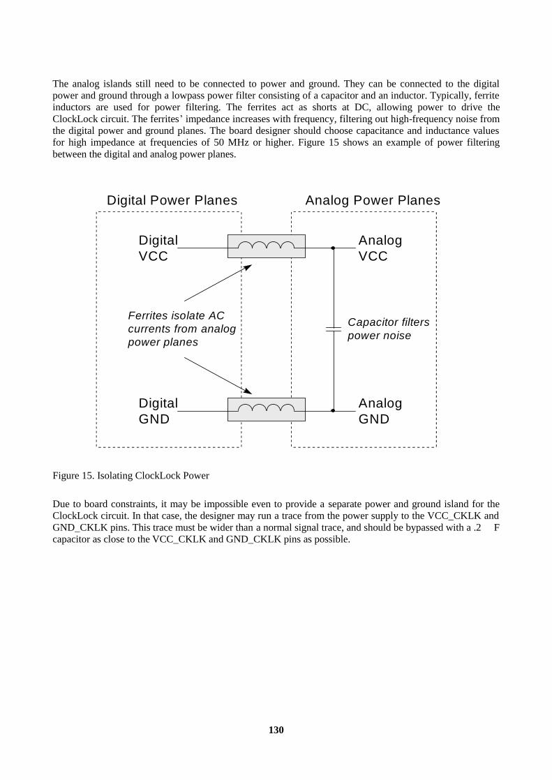
130
The analog islands still need to be connected to power and ground. They can be connected to the digital power and ground through a lowpass power filter consisting of a capacitor and an inductor. Typically, ferrite inductors are used for power filtering. The ferrites act as shorts at DC, allowing power to drive the ClockLock circuit. The ferrites’ impedance increases with frequency, filtering out high-frequency noise from the digital power and ground planes. The board designer should choose capacitance and inductance values for high impedance at frequencies of 50 MHz or higher. Figure 15 shows an example of power filtering between the digital and analog power planes.
Digital Power Planes Analog Power Planes
DigitalVCC
AnalogVCC
DigitalGND
AnalogGND
Ferrites isolate ACcurrents from analogpower planes
Capacitor filterspower noise
Figure 15. Isolating ClockLock Power Due to board constraints, it may be impossible even to provide a separate power and ground island for the ClockLock circuit. In that case, the designer may run a trace from the power supply to the VCC_CKLK and GND_CKLK pins. This trace must be wider than a normal signal trace, and should be bypassed with a .2 F capacitor as close to the VCC_CKLK and GND_CKLK pins as possible.

131
Conclusion Altera’s ClockLock and ClockBoost features address issues that affect high-density PLDs in the range of 100,000 gates or more. The ClockLock circuit locks onto the incoming clock and generates an internal clock, thus reducing clock delay and skew, and giving faster chip-to-chip performance. The ClockBoost feature adds clock multiplication, giving designers the capability to create time-domain multiplexed designs. Designers can also distribute a low-speed clock on the board, reducing layout issues. The MAX+PLUS II development software makes taking advantage of the ClockLock and ClockBoost features easy by providing an integrated solution for in-chip clock distribution. The combination of easy-to-use software and advanced on-chip clock management gives designers high performance at high densities. Design success with the ClockLock and ClockBoost circuits can be ensured by following the guidelines covered in this paper. References Siulinski, James A. “Design and layout rules eliminate noise coupling in communications systems,” EDN, June 20, 1996, pg. 95
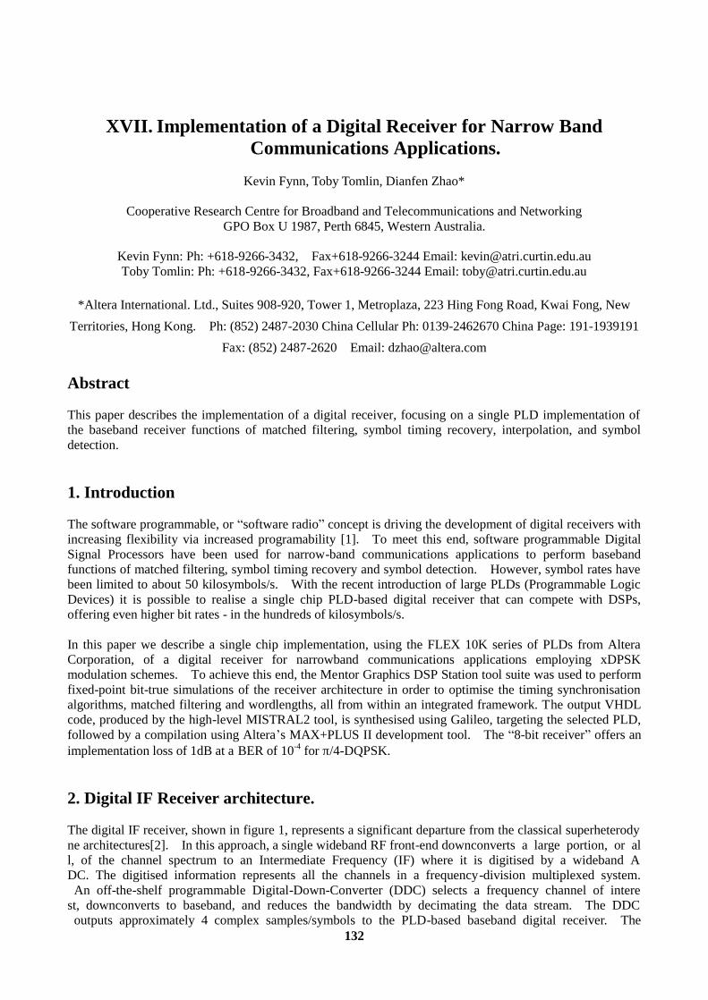
132
XVII. Implementation of a Digital Receiver for Narrow Band
Communications Applications.
Kevin Fynn, Toby Tomlin, Dianfen Zhao*
Cooperative Research Centre for Broadband and Telecommunications and Networking GPO Box U 1987, Perth 6845, Western Australia.
Kevin Fynn: Ph: +618-9266-3432, Fax+618-9266-3244 Email: [email protected] Toby Tomlin: Ph: +618-9266-3432, Fax+618-9266-3244 Email: [email protected]
*Altera International. Ltd., Suites 908-920, Tower 1, Metroplaza, 223 Hing Fong Road, Kwai Fong, New
Territories, Hong Kong. Ph: (852) 2487-2030 China Cellular Ph: 0139-2462670 China Page: 191-1939191 Fax: (852) 2487-2620 Email: [email protected]
Abstract
This paper describes the implementation of a digital receiver, focusing on a single PLD implementation of the baseband receiver functions of matched filtering, symbol timing recovery, interpolation, and symbol detection. 1. Introduction
The software programmable, or “software radio” concept is driving the development of digital receivers with increasing flexibility via increased programability [1]. To meet this end, software programmable Digital Signal Processors have been used for narrow-band communications applications to perform baseband functions of matched filtering, symbol timing recovery and symbol detection. However, symbol rates have been limited to about 50 kilosymbols/s. With the recent introduction of large PLDs (Programmable Logic Devices) it is possible to realise a single chip PLD-based digital receiver that can compete with DSPs, offering even higher bit rates - in the hundreds of kilosymbols/s. In this paper we describe a single chip implementation, using the FLEX 10K series of PLDs from Altera Corporation, of a digital receiver for narrowband communications applications employing xDPSK modulation schemes. To achieve this end, the Mentor Graphics DSP Station tool suite was used to perform fixed-point bit-true simulations of the receiver architecture in order to optimise the timing synchronisation algorithms, matched filtering and wordlengths, all from within an integrated framework. The output VHDL code, produced by the high-level MISTRAL2 tool, is synthesised using Galileo, targeting the selected PLD, followed by a compilation using Altera’s MAX+PLUS II development tool. The “8-bit receiver” offers an implementation loss of 1dB at a BER of 10-4 for π/4-DQPSK. 2. Digital IF Receiver architecture. The digital IF receiver, shown in figure 1, represents a significant departure from the classical superheterodyne architectures[2]. In this approach, a single wideband RF front-end downconverts a large portion, or all, of the channel spectrum to an Intermediate Frequency (IF) where it is digitised by a wideband ADC. The digitised information represents all the channels in a frequency-division multiplexed system. An off-the-shelf programmable Digital-Down-Converter (DDC) selects a frequency channel of interest, downconverts to baseband, and reduces the bandwidth by decimating the data stream. The DDC outputs approximately 4 complex samples/symbols to the PLD-based baseband digital receiver. The
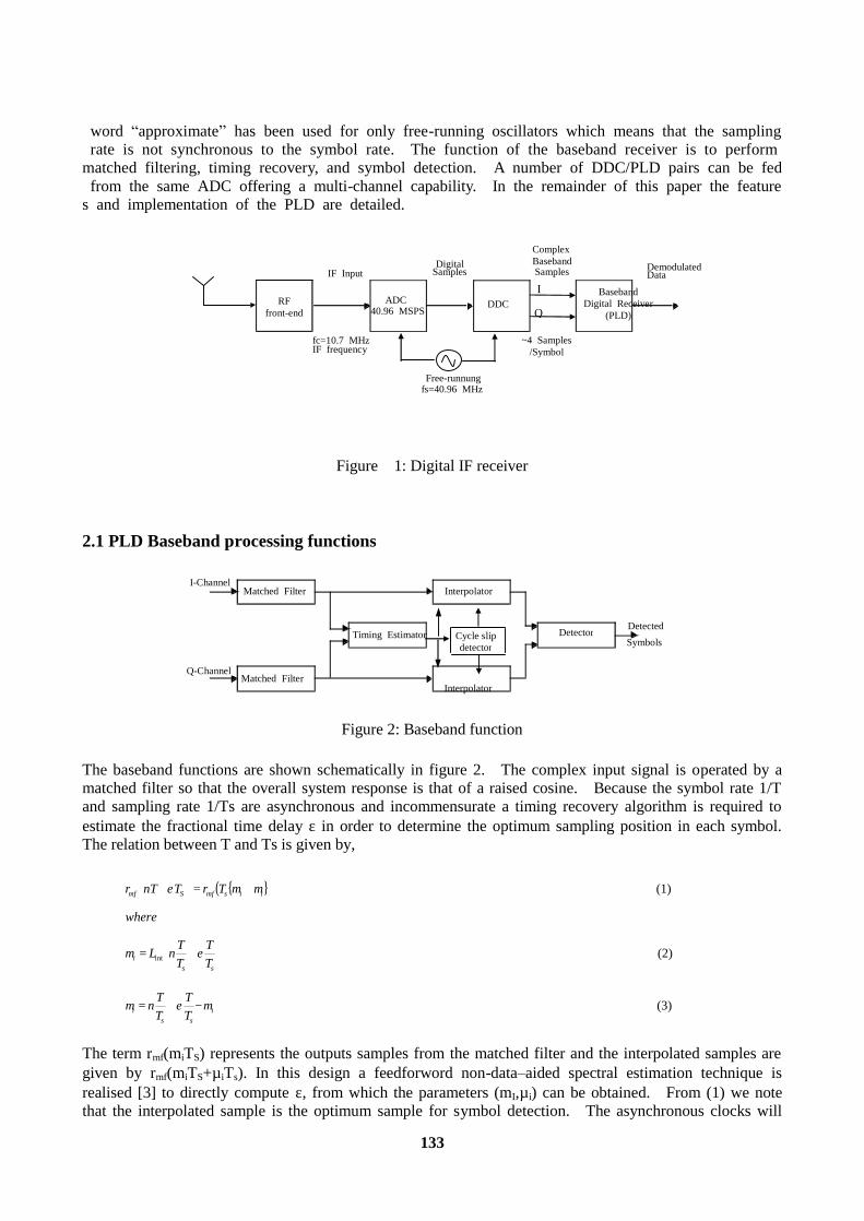
133
word “approximate” has been used for only free-running oscillators which means that the sampling rate is not synchronous to the symbol rate. The function of the baseband receiver is to perform matched filtering, timing recovery, and symbol detection. A number of DDC/PLD pairs can be fed from the same ADC offering a multi-channel capability. In the remainder of this paper the features and implementation of the PLD are detailed.
Figure 1: Digital IF receiver
2.1 PLD Baseband processing functions
Figure 2: Baseband function The baseband functions are shown schematically in figure 2. The complex input signal is operated by a matched filter so that the overall system response is that of a raised cosine. Because the symbol rate 1/T and sampling rate 1/Ts are asynchronous and incommensurate a timing recovery algorithm is required to estimate the fractional time delay ε in order to determine the optimum sampling position in each symbol. The relation between T and Ts is given by,
{ }( )
(3)
(2)
(1)
int
iss
i
ssi
iismfSmf
mTT
TTn
TT
TTnLm
where
mTrTnTr
−+=
+=
+=
+
∧
∧
∧
εµ
ε
µε
The term rmf(miTS) represents the outputs samples from the matched filter and the interpolated samples are given by rmf(miTS+µiTs). In this design a feedforword non-data–aided spectral estimation technique is realised [3] to directly compute ε, from which the parameters (mI,µi) can be obtained. From (1) we note that the interpolated sample is the optimum sample for symbol detection. The asynchronous clocks will
Matched Filter
Matched Filter
Timing Estimator
Interpolator
Detector
Interpolator
I-Channel
Q-Channel
Detected Symbols
Q
I ADC DDC
Baseband Digital Receiver
(PLD)
IF Input Digital Samples
Complex Baseband Samples Demodulated
Data
fc=10.7 MHz IF frequency
40.96 MSPS
fs=40.96 MHz Free-runnung
~4 Samples /Symbol
RF front-end
Cycle slip detector
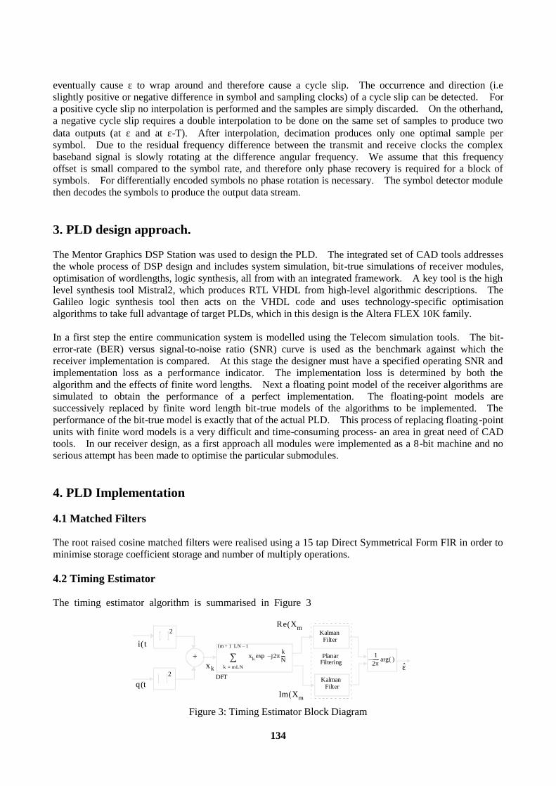
134
eventually cause ε to wrap around and therefore cause a cycle slip. The occurrence and direction (i.e slightly positive or negative difference in symbol and sampling clocks) of a cycle slip can be detected. For a positive cycle slip no interpolation is performed and the samples are simply discarded. On the otherhand, a negative cycle slip requires a double interpolation to be done on the same set of samples to produce two data outputs (at ε and at ε-T). After interpolation, decimation produces only one optimal sample per symbol. Due to the residual frequency difference between the transmit and receive clocks the complex baseband signal is slowly rotating at the difference angular frequency. We assume that this frequency offset is small compared to the symbol rate, and therefore only phase recovery is required for a block of symbols. For differentially encoded symbols no phase rotation is necessary. The symbol detector module then decodes the symbols to produce the output data stream. 3. PLD design approach. The Mentor Graphics DSP Station was used to design the PLD. The integrated set of CAD tools addresses the whole process of DSP design and includes system simulation, bit-true simulations of receiver modules, optimisation of wordlengths, logic synthesis, all from with an integrated framework. A key tool is the high level synthesis tool Mistral2, which produces RTL VHDL from high-level algorithmic descriptions. The Galileo logic synthesis tool then acts on the VHDL code and uses technology-specific optimisation algorithms to take full advantage of target PLDs, which in this design is the Altera FLEX 10K family. In a first step the entire communication system is modelled using the Telecom simulation tools. The bit-error-rate (BER) versus signal-to-noise ratio (SNR) curve is used as the benchmark against which the receiver implementation is compared. At this stage the designer must have a specified operating SNR and implementation loss as a performance indicator. The implementation loss is determined by both the algorithm and the effects of finite word lengths. Next a floating point model of the receiver algorithms are simulated to obtain the performance of a perfect implementation. The floating-point models are successively replaced by finite word length bit-true models of the algorithms to be implemented. The performance of the bit-true model is exactly that of the actual PLD. This process of replacing floating-point units with finite word models is a very difficult and time-consuming process- an area in great need of CAD tools. In our receiver design, as a first approach all modules were implemented as a 8-bit machine and no serious attempt has been made to optimise the particular submodules. 4. PLD Implementation 4.1 Matched Filters The root raised cosine matched filters were realised using a 15 tap Direct Symmetrical Form FIR in order to minimise storage coefficient storage and number of multiply operations. 4.2 Timing Estimator The timing estimator algorithm is summarised in Figure 3
Figure 3: Timing Estimator Block Diagram
xk j2πkN----–
exp
k mLN=
m 1+( )LN 1–
∑ 12π------ ( )arg–+
2
2
PlanarFiltering
KalmanFilter
KalmanFilter
ε̂
Re Xm( )
Im Xm( )q t( )
i t( )
xkDFT
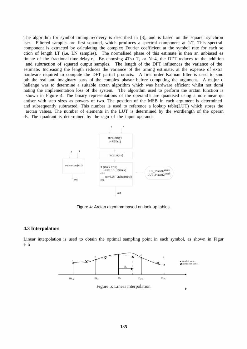
135
The algorithm for symbol timing recovery is described in [3], and is based on the squarer synchroniser. Filtered samples are first squared, which produces a spectral component at 1/T. This spectral component is extracted by calculating the complex Fourier coefficient at the symbol rate for each section of length LT (i.e. LN samples). The normalised phase of this estimate is then an unbiased estimate of the fractional time delay ε. By choosing 4Ts≈ T, or N=4, the DFT reduces to the addition and subtraction of squared output samples. The length of the DFT influences the variance of the estimate. Increasing the length reduces the variance of the timing estimate, at the expense of extra hardware required to compute the DFT partial products. A first order Kalman filter is used to smooth the real and imaginary parts of the complex phasor before computing the argument. A major challenge was to determine a suitable arctan algorithm which was hardware efficient whilst not dominating the implementation loss of the system. The algorithm used to perform the arctan function is shown in Figure 4. The binary representations of the operand’s are quantised using a non-linear quantiser with step sizes as powers of two. The position of the MSB in each argument is determined and subsequently subtracted. This number is used to reference a lookup table(LUT) which stores the arctan values. The number of elements in the LUT is determined by the wordlength of the operands. The quadrant is determined by the sign of the input operands.
Figure 4: Arctan algorithm based on look-up tables.
4.3 Interpolators Linear interpolation is used to obtain the optimal sampling point in each symbol, as shown in Figure 5
Figure 5: Linear interpolation
m=MSB(y)n=MSB(x)
index=(y-x)
if (index >= 0)out=LUT_1(index)
elseout=LUT_2(abs(index))
end
y x
out
out=arctan(y/x)
y x
out
LUT_1=atan(2index)LUT_2=atan(2- index)
sampled values interpolated values
a e d c
b
µι
mi mi-1 mi-2 mi+1 mi+2
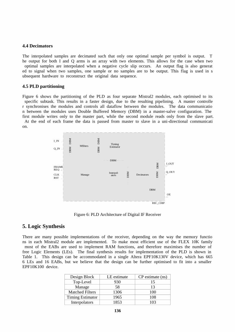
136
4.4 Decimators The interpolated samples are decimated such that only one optimal sample per symbol is output. The output for both I and Q arms is an array with two elements. This allows for the case when two optimal samples are interpolated when a negative cycle slip occurs. An output flag is also generated to signal when two samples, one sample or no samples are to be output. This flag is used in subsequent hardware to reconstruct the original data sequence. 4.5 PLD partitioning Figure 6 shows the partitioning of the PLD as four separate Mistral2 modules, each optimised to its specific subtask. This results in a faster design, due to the resulting pipelining. A master controller synchronises the modules and controls all dataflow between the modules. The data communication between the modules uses Double Buffered Memory (DBM) in a master-salve configuration. The first module writes only to the master part, while the second module reads only from the slave part. At the end of each frame the data is passed from master to slave in a uni-directional communication.
Figure 6: PLD Architecture of Digital IF Receiver
5. Logic Synthesis There are many possible implementations of the receiver, depending on the way the memory functions in each Mistral2 module are implemented. To make most efficient use of the FLEX 10K family most of the EABs are used to implement RAM functions, and therefore maximises the number of free Logic Elements (LEs). The final synthesis results for implementation of the PLD is shown in Table 1. This design can be accommodated in a single Altera EPF10K130V device, which has 6656 LEs and 16 EABs, but we believe that the design can be further optimised to fit into a smaller EPF10K100 device.
Design Block LE estimate CP estimate (ns) Top-Level 930 15 Manage 58 13
Matched Filters 1306 100 Timing Estimator 1965 108
Interpolators 1853 103
MfiltersTiming
Estimator
Interpol-DecimatorsManage
DB
M
DBM
DB
M
DB
MD
BM
DB
M
DB
MD
BM
DBM
REC_CHIP
ators
I_IN
Q_IN
FRAMEREQ
I_OUT
Q_OUT
OE
CLKRST

137
Decimators 453 38 Total 6565 108
Table 1: Logic synthesis of the PLD baseband modules
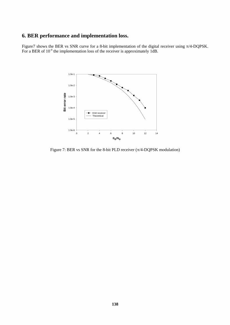
138
6. BER performance and implementation loss. Figure7 shows the BER vs SNR curve for a 8-bit implementation of the digital receiver using π/4-DQPSK. For a BER of 10-4 the implementation loss of the receiver is approximately 1dB.
Figure 7: BER vs SNR for the 8-bit PLD receiver (π/4-DQPSK modulation)
Eb/No
0 2 4 6 8 10 12 14
Bit
erro
r rat
e
1.0e-6
1.0e-5
1.0e-4
1.0e-3
1.0e-2
1.0e-1
8-bit receiverTheoretical

139
Conclusions This paper describes a single-chip PLD implementation of the baseband processing functions of digital-IF receiver, using Mentor Graphic’s DSP Station tool suite as the design environment. This suite of tools provides an excellent integrated frame work for data management, design simulation, algorithm optimisation, and to model the bit-true performance of a DSP algorithm. The target PLD was Altera FLEX 10K series because of its EAB features. The final design was partitioned into 4 modules for increased pipelining. With the current architecture and synthesis the receiver can work at bit rates of up to 100 kbit/s with a 10 MHz clock frequency. With the experience gained from using the Mistral2 software tool, it would be more efficient to use hand coded VHDL for the time/area critical operations on the datapath. Mistral2 is excellent as an interconnect framework, and controller generator. This would result in designs with a much faster datapath and a significantly smaller microrom because of the dual advantage reducing the schedule length and the microrom word width. In addition further improvements can be achieved by better partitioning of the design. For example the timing estimator could be partitioned into two further sub-modules, one to perform the DFT, and the other to perform the planar filtering and arctan function. The resulting module would be smaller and faster than the existing timing estimator. With the current design it is possible to realise a single-chip PLD solution using a EPF10K130V device and it is not unrealistic to expect that with the improvements suggested above the design can be ported to smaller lower-cost PLDs such as the EPF10K100 device. We expect that with the increased pipelining bit-rates of up to 1 Mbit/s could be supported. References 1. J. Miola, “The Sotware Radio Architecture”, IEEE Communications Magazine, May 1995, pp26-38 2. H. Meyr and Ravi Subramanian, “Advanced Digital Receiver Principles and Technologies for PCS”,
IEEE Communications magazine, Jan 1995, pp68-78 3. Martin Oerder and Heinrich Meyr, “Digital Filter and Square Timing Recovery”, IEEE trans. on
Communications, Vol. 36. No. 5. May 1988
140
XVIII. Image Processing in Altera FLEX 10K Devices
Martin Langhammer, Kaytronics Inc.
Caleb Crome, Altera Corporation
Introduction This paper will examine several methods by which programmable logic may be employed to implement image processing acceleration applications, particularly for unique requirements. Transform coding will be the primary focus, with quantization only considered when necessary for illustration. After a discussion of possible cases where custom solutions may be warranted, and a brief overview of new programmable logic devices and their suitability for image processing, some common transforms will be shown in the context of programmable logic implementations. 1. Why Use Programmable Logic? Although high volume consumer products such as JPEG and MPEG now may be designed using standard, off-the-shelf components, there are many industrial applications where unique requirements dictate that a custom solution be provided. Examples include: Non-standard Sizes – While MPEG and JPEG typically provide for only common interchange formats, such as CCIR 601, some medical applications involve image sizes up to 4K by 4K pixels, non-interlaced. Frame Rate – Processing may be required in excess of 30 fps, such as when real time or accelerated processing of high speed (slow motion) image sequences is needed. Quality – If high quality image reproduction is not required, a simpler transform may be used for compression. On the other hand, a special form of quantization may be required to provide extraordinary image fidelity. Operations – Other operations, such as image resizing, may be required at the same time as compression. Both operations may be performed during the processing of the transform, rather than separately. Image Formats – Front-end processing can be implemented in programmable logic to convert the image format, or the transform can be easily recast to handle the incoming format. Changing Requirements – If several different flows are expected, an entirely new image processing engine can be configured, in circuit. Previously, such requirements in real time often dictated the use of multiple DSPs or other processors, or else ASICs with their associated development time, hidden costs, and high risk. Programmable logic also brings benefits during MPEG development. By implementing the functional blocks required for this standard in real time, such as the DCT, IDCT, Q, IQ, MS/ME, and MC, real time system prototyping, or even test equipment, is now possible. 2. Altera FLEX 10K CPLD The Altera FLEX 10K has some unique features particularly suited to image processing. The EAB, or embedded array block, may be configured as a fast static RAM, with better than 50 MHz throughput. Its size, at 256x8 bits, is significant for image processing in several ways; the 256 location size is the same size as an MPEG macroblock with two luminance and two chrominance blocks, in 4:2:2 format, or the 16 by 16 search

141
area for the MPEG ME operation. For other standards, four 8 by 8, or one 16 by 16 pixel block can be contained in one EAB. If a larger precision than 8 bits is required, multiple EABs may be accessed in parallel. In addition, four DCT quantization tables, or a JPEG or MPEG Huffman coding table may be fitted into EABs. Many two-dimensional image processing transforms can be implemented as separable transforms, i.e. intermediate values will be generated, and must be stored in some form of transposition memory. The relatively small EAB, with extremely fast access capability, can store one or several blocks of intermediate values. Direct 2D implementation separable transforms are also possible. Although very fast, they are generally very large, and ungainly to implement in hardware [3]. 3. Image Transform Examples
3.1 Walsh Transform The Walsh transform is a simple example of an image processing transform that may be optimized for a programmable logic implementation. The Walsh transform is
W u vN
f x yy
N
x
Nb x b u b y b v
i
Ni n l i i n l i( , ) ( , ) ( )[ ( ) ( ) ( ) ( )]= −
=
−
=
−+
=
−
∑∑ ∏ − − − −1
10
1
0
1
0
1
which is a square matrix with orthogonal rows and columns. In the case of the common image block coding size of 8 by 8 pixels, it is of the form (1D)
W =18
1 1 1 1 1 1 1 11 1 1 1 -1 -1 -1 -11 1 -1 -1 -1 -1 1 11 1 -1 -1 1 1 -1 -11 -1 -1 1 1 -1 -1 11 -1 -1 1 -1 1 1 -11 -1 1 -1 -1 1 -1 11 -1 1 -1 1 -1 1 -1
when presented in ordered sequence, i.e. increasing frequency per row. This form is sometimes referred to as the Walsh-Hadamard form. This matrix can be decomposed into a number of more sparse matrixes, again containing only adds and subtracts, which can be used for the efficient implementation of an image processing engine in programmable logic. The following simulation will serve to illustrate the Walsh transform. A simple zonal coding will be used for quantization, where only the F(0,2) block of frequency values will be retained, for an approximate compression ratio of 7:1. The compressed image is then decompressed with the inverse Walsh transform, which is of the same form as the forward transform.
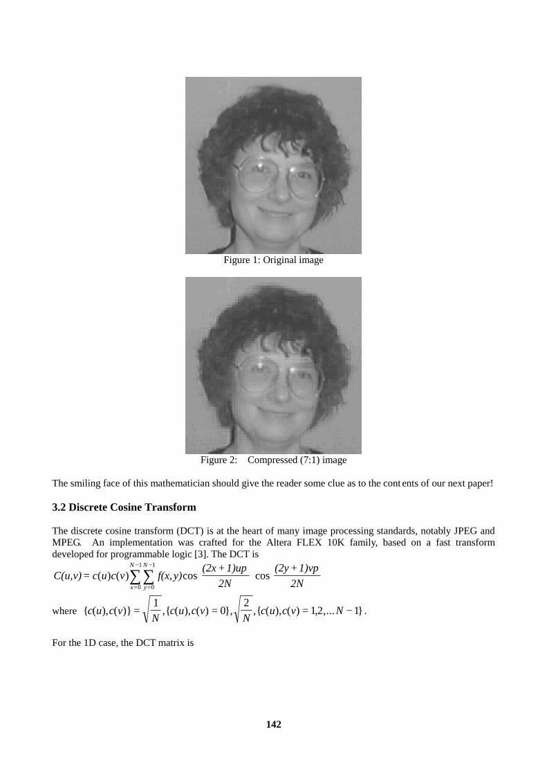
142
Figure 1: Original image
Figure 2: Compressed (7:1) image
The smiling face of this mathematician should give the reader some clue as to the cont ents of our next paper! 3.2 Discrete Cosine Transform The discrete cosine transform (DCT) is at the heart of many image processing standards, notably JPEG and MPEG. An implementation was crafted for the Altera FLEX 10K family, based on a fast transform developed for programmable logic [3]. The DCT is
C(u,v)= c u c v f(x,y)(2x +1)u
2N(2y +1)v
2Ny
N
x
N
( ) ( ) cos cosπ π
=
−
=
−
∑∑0
1
0
1
where { ( ), ( )} ,{ ( ), ( ) }, ,{ ( ), ( ) , ,... }c u c vN
c u c vN
c u c v N= = = −1
02
12 1 .
For the 1D case, the DCT matrix is
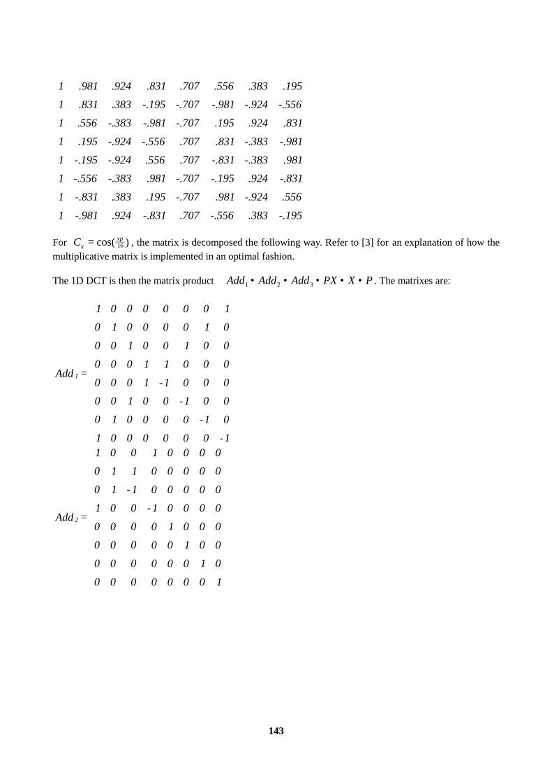
143
1 .981 .924 .831 .707 .556 .383 .1951 .831 .383 -.195 -.707 -.981 -.924 -.5561 .556 -.383 -.981 -.707 .195 .924 .8311 .195 -.924 -.556 .707 .831 -.383 -.9811 -.195 -.924 .556 .707 -.831 -.383 .9811 -.556 -.383 .981 -.707 -.195 .924 -.8311 -.831 .383 .195 -.707 .981 -.924 .5561 -.981 .924 -.831 .707 -.556 .383 -.195
For Cx
x= cos( )π16 , the matrix is decomposed the following way. Refer to [3] for an explanation of how the
multiplicative matrix is implemented in an optimal fashion. The 1D DCT is then the matrix product Add Add Add PX X P1 2 3• • • • • . The matrixes are:
1Add =
1 0 0 0 0 0 0 10 1 0 0 0 0 1 00 0 1 0 0 1 0 00 0 0 1 1 0 0 00 0 0 1 -1 0 0 00 0 1 0 0 -1 0 00 1 0 0 0 0 -1 01 0 0 0 0 0 0 -1
2Add =
1 0 0 1 0 0 0 00 1 1 0 0 0 0 00 1 - 1 0 0 0 0 01 0 0 - 1 0 0 0 00 0 0 0 1 0 0 00 0 0 0 0 1 0 00 0 0 0 0 0 1 00 0 0 0 0 0 0 1
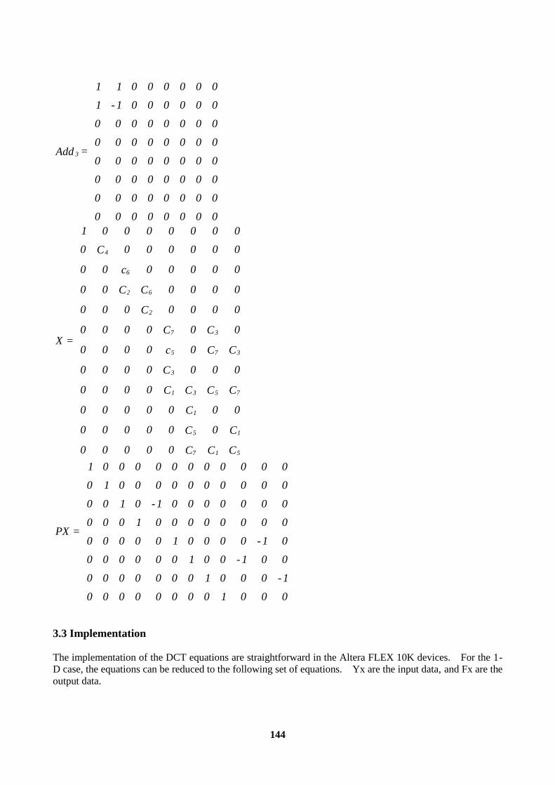
144
3Add =
1 1 0 0 0 0 0 01 - 1 0 0 0 0 0 00 0 0 0 0 0 0 00 0 0 0 0 0 0 00 0 0 0 0 0 0 00 0 0 0 0 0 0 00 0 0 0 0 0 0 00 0 0 0 0 0 0 0
X =
1 0 0 0 0 0 0 00 C 0 0 0 0 0 0
0 0 c 0 0 0 0 0
0 0 C C 0 0 0 0
0 0 0 C 0 0 0 0
0 0 0 0 C 0 C 0
0 0 0 0 c 0 C C
0 0 0 0 C 0 0 0
0 0 0 0 C C C C
0 0 0 0 0 C 0 0
0 0 0 0 0 C 0 C
0 0 0 0 0 C C C
4
6
2 6
2
7 3
5 7 3
3
1 3 5 7
1
5 1
7 1 5
PX =
1 0 0 0 0 0 0 0 0 0 0 00 1 0 0 0 0 0 0 0 0 0 00 0 1 0 - 1 0 0 0 0 0 0 00 0 0 1 0 0 0 0 0 0 0 00 0 0 0 0 1 0 0 0 0 - 1 00 0 0 0 0 0 1 0 0 - 1 0 00 0 0 0 0 0 0 1 0 0 0 - 10 0 0 0 0 0 0 0 1 0 0 0
3.3 Implementation The implementation of the DCT equations are straightforward in the Altera FLEX 10K devices. For the 1-D case, the equations can be reduced to the following set of equations. Yx are the input data, and Fx are the output data.

145
Stage1: A1 = X1 + X8 A2 = X2 + X7 A3 = X3 + X6 A4 = X4 + X5 A5 = X4 - X5 A6 = X3 - X6 A7 = X2 - X7 A8 = X1 - X8 Stage2: B1 = A1 + A4 B2 = A2 + A3 B3 = A2 - A3 B4 = A1 - A4 B5 = A5 B6 = A6 B7 = A7 B8 = A8 Stage3: C1 = B1 + B2 C2 = B1 - B2 C3 = B3 C4 = B4 C5 = B5 C6 = B6 C7 = B7 C8 = B8 C9 = -C3 = -B3 C10 = -C6 = -B6 C11 = -C5 = -B5 C12 = -C7 = -B7 Stage4: D1 = C1 D2 = C2 D3 = C3 D4 = C4 D5 = -C3 = C9 D6 = C5 D7 = C6 D8 = C7 D9 = C8 D10= -C6 = C10 D11= -C5 = C11 D12= -C7 = C12 Vector Stage E1 = D1 E2 = D2 . X6
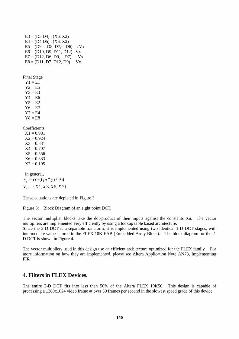
146
E3 = (D3,D4) . (X6, X2) E4 = (D4,D5) . (X6, X2) E5 = (D9, D8, D7, D6) . Vx E6 = (D10, D9, D11, D12) . Vx E7 = (D12, D6, D9, D7) . Vx E8 = (D11, D7, D12, D9) .Vx Final Stage Y1 = E1 Y2 = E5 Y3 = E3 Y4 = E6 Y5 = E2 Y6 = E7 Y7 = E4 Y8 = E8 Coefficients: X1 = 0.981 X2 = 0.924 X3 = 0.831 X4 = 0.707 X5 = 0.556 X6 = 0.383 X7 = 0.195 In general, x pi yy = cos(( * ) / )16 V X X X Xx = { , , , }1 3 5 7 These equations are depicted in Figure 3. Figure 3: Block Diagram of an eight point DCT. The vector multiplier blocks take the dot-product of their inputs against the constants Xn. The vector multipliers are implemented very efficiently by using a lookup table based architecture. Since the 2-D DCT is a separable transform, it is implemented using two identical 1-D DCT stages, with intermediate values stored in the FLEX 10K EAB (Embedded Array Block). The block diagram for the 2-D DCT is shown in Figure 4. The vector multipliers used in this design use an efficient architecture optimized for the FLEX family. For more information on how they are implemented, please see Altera Application Note AN73, Implementing FIR 4. Filters in FLEX Devices. The entire 2-D DCT fits into less than 50% of the Altera FLEX 10K50. This design is capable of processing a 1280x1024 video frame at over 30 frames per second in the slowest speed grade of this device.
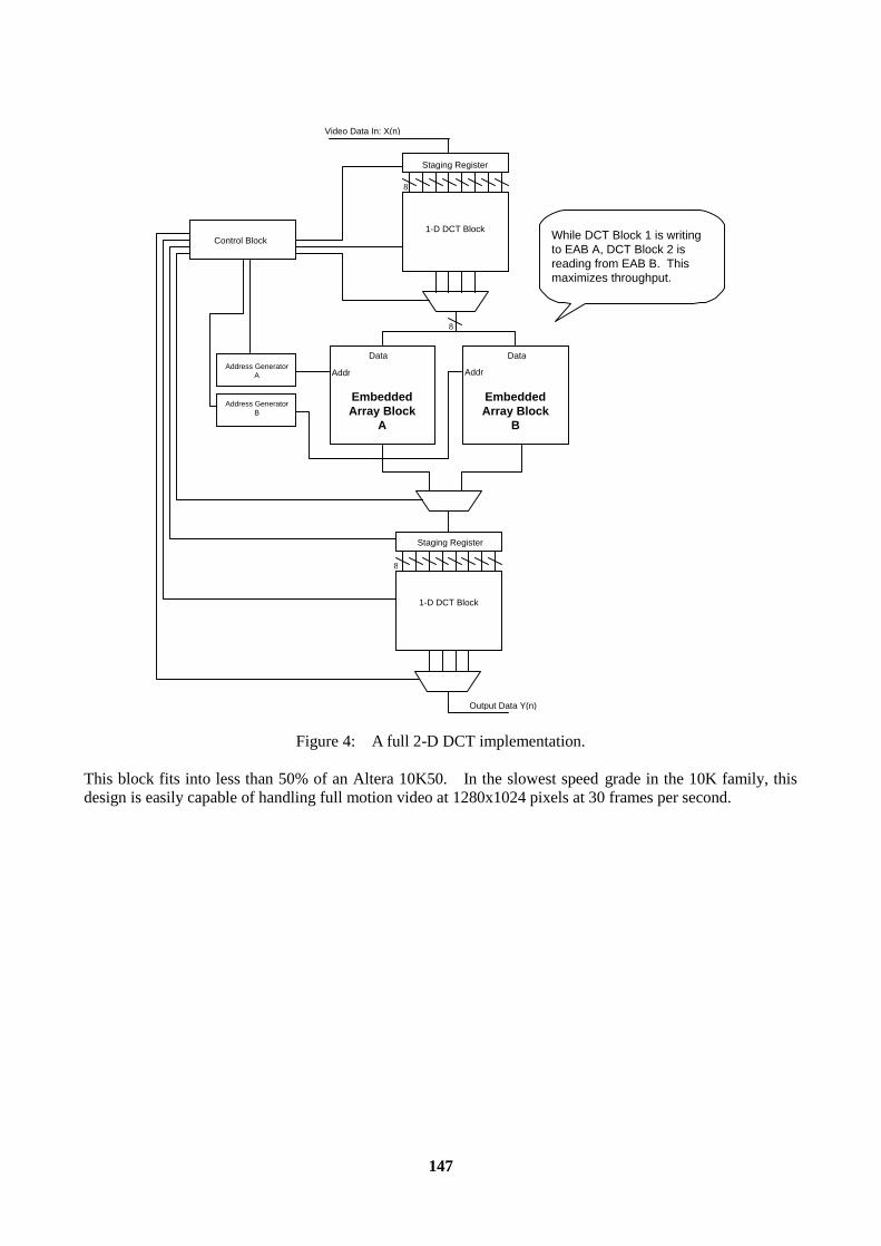
147
8
Video Data In: X(n)
8
Data
Addr Addr
Data
Staging Register
8
Output Data Y(n)
Control Block While DCT Block 1 is writingto EAB A, DCT Block 2 isreading from EAB B. Thismaximizes throughput.
EmbeddedArray Block
B
EmbeddedArray Block
A
Staging Register
1-D DCT Block
Address GeneratorA
Address GeneratorB
1-D DCT Block
Figure 4: A full 2-D DCT implementation. This block fits into less than 50% of an Altera 10K50. In the slowest speed grade in the 10K family, this design is easily capable of handling full motion video at 1280x1024 pixels at 30 frames per second.

148
Conclusion Optimizing image processing transforms for implementation in the Altera FLEX 10K architecture results in an extremely fast and flexible solution for video DSP applications. Here we covered the Walsh transform and the DCT. We have implemented a DCT that is capable of very high speed operation and moderate silicon resources. These examples illustrate real-time system-level functionality now possible with large programmable logic devices such as the 10K family. References
1. W. K. Pratt, "Digital Image Processing", John Wiley & Sons, Inc., New York, 1991 2. R. C. Gonzalez, R.E. Woods, "Digital Image Processing", Addison Wesley, Reading, MA., 1993 3. M. Langhammer, "Optimal DCT for Hardware”, Proceedings, ICSPAT '95, 1995 4. W. B. Pennebaker, J. L. Mitchell, "JPEG Still Image Compression Standard", Van Nostrand Reinhold,
New York, 1993
149
XIX. The Importance of JTAG and ISP in Programmable Logic
Robert K. Beachler Manager, Strategic Marketing and Communications
Altera Corporation Programmable logic has become the bedrock of digital design. The benefits that a programmable solution brings, such as design flexibility, fast development times, and inventory risk reduction have propelled these devices into mainstream usage. No longer are programmable devices used for small production volumes, rather, these high-capacity devices are now used in significant volume applications, such as laptop computers, networking cards, and even automobiles. The increasing usage in volume applications brings new device feature demands typically outside the scope of low-volume products. Such aspects as streamlining the manufacturing flow, improving testability, and allowing for field modifications are vitally important to product success, but until recently may not have been part of the development of new PLD architectures. The increased capacity, pin counts, and volumes of PLDs have combined to require suppliers of high capacity devices to develop new devices that fit the needs of not only the design engineer, but also the production and quality engineers as well. The new MAX 9000 family of programmable logic devices from Altera solves these problems by offering both JTAG circuitry for testing and in-system programming (ISP) for manufacturing. 1. Packaging, Flexibility Drive In-System Programmability Adoption As programmable logic devices increase in capacity, so does the number of I/O pins per device. This requires careful consideration on the part of the PLD vendor when selecting package options. The selection for high-volume, high-pin count packages is limited. Pin grid array packages are the easiest to use, but unfortunately they are also quite expensive, and have a large footprint, which consumes board space. Quad flat pack packages are by far the most popular package for high-pin count devices, as they are relatively inexpensive, and offer a small footprint. However, QFP packages are very fragile, and the leads deform quite easily. This is a distinct problem for programmable devices, which typically need to be inserted into a programmer for programming. Altera provided a solution to this problem with a QFP carrier technology that protects the leads during handling and programming. The emergence of in-system programming (ISP) is a complementary solution to this problem. With an ISP devices, such as the MAX 9000 family, the devices may be soldered directly to the PC board before programming. The device may then be programmed multiple times on the board using standard 5-Volt signals. Internal to an ISP device are charge pumps that provide the high voltage level necessary to program the EEPROM cells. 2. Prototyping Flexibility During the engineering phase of a project, ISP may be used to quickly change the circuitry of the system without ever having to change the board layout. As design errors are uncovered, the designers may change their design and download to the board the new design, with the corrected design. One important aspect of this approach is that the pinouts of the device cannot change, as this would necessitate a board layout change, costly in both money and time. Therefore, Altera designed the MAX 9000 devices with ISP in mind, adding the necessary routing resources so that engineers may permute their design without having to change the device pinout. ISP devices currently offered by other vendors do not offer this capability, and in many situations a board change is necessary.
150
Additionally, companies may use this capability for unique situations to customize the board. For example, an add-in card manufacturer may wish to do a PCI and EISA-bus compliant version of its product. Rather than designing two distinct products, the bus interface design may be accomplished in an ISP device. At the manufacturing level, the device may be programmed with either the PCI interface design or the EISA interface design, saving cost and decreasing inventory risk. ISP also offers the ability to do field upgrades of systems where hardware changes may be sent via floppy disk, network, or modem. 3. ISP Benefits to Manufacturing The manufacturing flow using programmable devices is currently somewhat cumbersome. The current production method for non-volatile programmable devices is to program the devices first, place them in inventory, and then place them in the board during production, and then test the board. With ISP devices, the device is soldered directly onto the board, and may then be programmed using a download cable or with the board tester itself. The ability to program a MAX 9000 device in the system multiple times expands the capability of the manufacturing process. In many situations, a company may choose to place a test design into the PLD, using the PLD as an integrated part of the testing procedure, and after testing is complete, place the actual production design into the device. 4. Decreasing Board Size, Increasing Complexity Drive Adoption of JTAG Boundary Scan The decreasing size of printed circuit boards, enabled by the advances in surface-mount packages, has resulted in difficult board testing issues. Traditional testing methods consisted of testing devices before insertion onto the board, and once the board is manufactured, numerous contact points were placed upon the board for a board tester to attach to the wire traces on the board. This “bed-of-nails” testing methodology requires significant board space and can sometimes cause continuity and pin shorting, as well as electrical overstress caused by back driving devices. In the 1980’s, the Joint Test Action Group (JTAG) developed the IEEE 1149.1-1990 specification for boundary-scan testing. The Boundary-Scan Test (BST) architecture developed offers the capability to efficiently test components on circuit boards. As shown in Figure 1, the JTAG methodology consists of a series of scan registers at the I/O pins of the device. Printed circuit boards developed with JTAG compliant devices allow the testing of a single device, the connections between devices, and functional tests. 5. JTAG Defined The JTAG specification defines 5 signals used to control the operation of the boundary-scan registers. The JTAG signals are described in Table 1. With these signals and the associated commands designers may develop test procedures to check the functionality of specific devices, as well as the entire board.
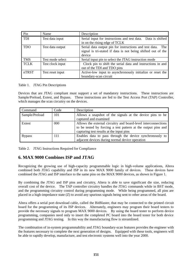
151
Pin Name Description TDI Test data input Serial input for instructions and test data. Data is shifted
in on the rising edge of TCLK TDO Test data output Serial data output pin for instructions and test data. The
signal is tri-stated if data is not being shifted out of the device
TMS Test mode select Serial input pin to select the JTAG instruction mode TCLK Test clock input Clock pin to shift the serial data and instructions in and
out of the TDI and TDO pins nTRST Test reset input Active-low input to asynchronously initialize or reset the
boundary-scan circuit Table 1. JTAG Pin Descriptions Devices that are JTAG compliant must support a set of mandatory instructions. These instructions are Sample/Preload, Extest, and Bypass. These instructions are fed to the Test Access Port (TAP) Controller, which manages the scan circuitry on the devices.
Command Code Description Sample/Preload 101 Allows a snapshot of the signals at the device pins to be
captured and examined Extest 000 Allows the external circuitry and board-level interconnections
to be tested by forcing a test pattern at the output pins and capturing test results at the input pins
Bypass 111 Enables data to pass through the device synchronously to adjacent devices during normal device operation
Table 2. JTAG Instructions Required for Compliance 6. MAX 9000 Combines ISP and JTAG Recognizing the growing use of high-capacity programmable logic in high-volume applications, Altera combined both JTAG capability and ISP in its new MAX 9000 family of devices. These devices have combined the JTAG and ISP interface to the same pins on the MAX 9000 devices, as shown in Figure 1. By combining the JTAG and ISP pins and circuitry, Altera is able to save significant die size, reducing overall cost of the device. The TAP controller circuitry handles the JTAG commands while in BST mode, and the programming circuitry control during programming mode. While being programmed, all pins are placed in a high-impedance state (Z) to avoid any spurious signals being sent to other areas of the board. Altera offers a serial port download cable, called the BitBlaster, that may be connected to the printed circuit board for the programming of its ISP devices. Alternately, engineers may program their board testers to provide the necessary signals to program MAX 9000 devices. By using the board tester to perform device programming, companies need only to insert the completed PC board into the board tester for both device programming and JTAG testing. In this way the manufacturing flow is streamlined. The combination of in-system programmability and JTAG boundary-scan features provides the engineer with the features necessary to complete the next generation of designs. Equipped with these tools, engineers will be able to rapidly develop, manufacture, and test electronic systems well into the year 2000.
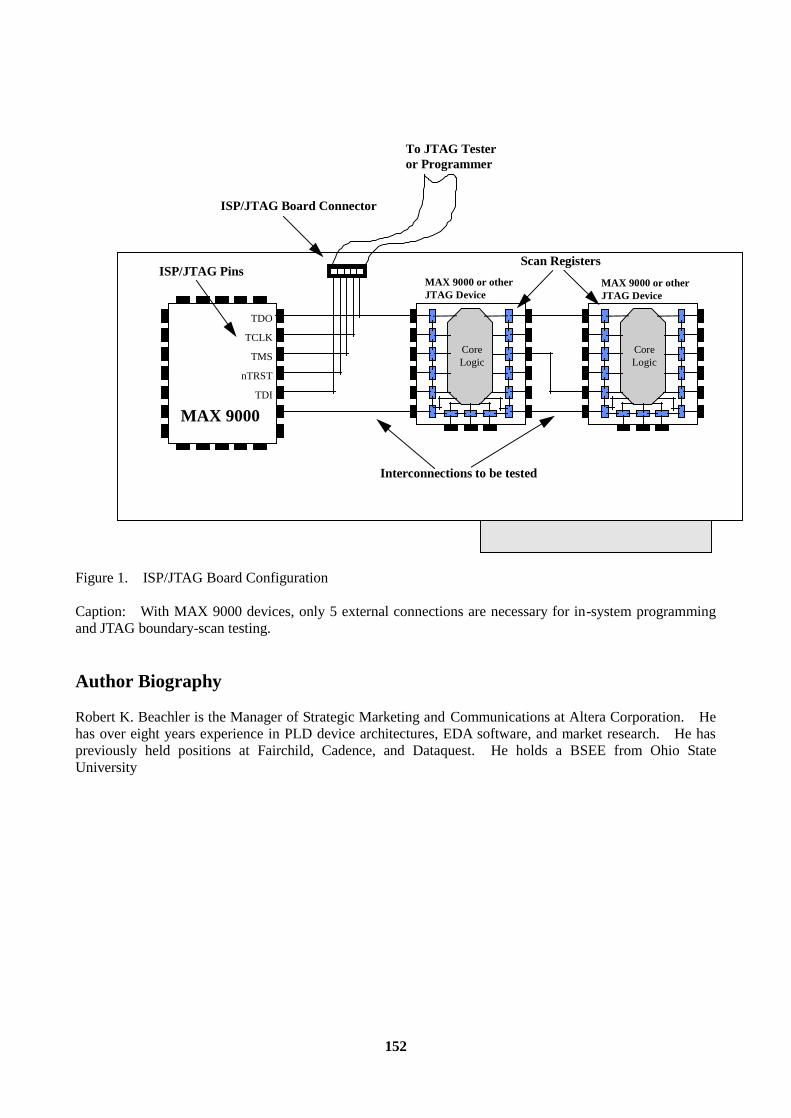
152
Figure 1. ISP/JTAG Board Configuration Caption: With MAX 9000 devices, only 5 external connections are necessary for in-system programming and JTAG boundary-scan testing. Author Biography Robert K. Beachler is the Manager of Strategic Marketing and Communications at Altera Corporation. He has over eight years experience in PLD device architectures, EDA software, and market research. He has previously held positions at Fairchild, Cadence, and Dataquest. He holds a BSEE from Ohio State University
TCLK
MAX 9000
CoreLogic
TDO
TMS
TDI
nTRST
CoreLogic
ISP/JTAG Board Connector
ISP/JTAG PinsScan Registers
Interconnections to be tested
MAX 9000 or otherJTAG Device
MAX 9000 or otherJTAG Device
To JTAG Testeror Programmer
153
XX. Reed Solomon Codec Compiler for Programmable Logic
Martin Langhammer
Kaytronics, Inc.
405 Britannia Rd. E. #206 Mississauga, Ontario, Canada
L4Z 3E6
This paper describes the use and results of a Reed Solomon codec macro generator optimized for programmable logic. The design of several differing codecs is detailed, along with analysis of resource requirements, and codec performance. 1. INTRODUCTION The Reed Solomon codec compiler described in this paper can generate Reed Solomon encoders and decoders for a wide variety of codes, detailed below in the parameters section. Once the code has been created by the utility, the top level HDL file may be compiled, targeting an Altera 10K device. Typically, and encoder will compile, including fitting and routing, in less than one minute, and a decoder will compile within five minutes. The utility program will also generate testcases, to functionally verify the cores created. There are three Reed Solomon Codec macros; one encoder and two decoders, which are optimized for different size/performance tradeoffs. The lower performance, or discrete decoder, receives a codeword, calculates error locations and values, and writes out a corrected codeword. The higher performance, or streaming decoder, continually reads in, and writes out, codewords. The streaming decoder uses only marginally more logic, but requires a greater amout of memory, as the performance improvement is largely due to system pipelining between decoder blocks. 2. PARAMETERS A Reed Solomon code can be defined by the following parameters: 2.1 TOTAL NUMBER OF SYMBOLS PER CODEWORD There may be up to 2m –1 number of symbols per codeword, also known as N. For the Reed Solomon compiler, N must be greater than 3, subject to a minimum of R + 1. 2.2 NUMBER OF CHECK SYMBOLS The compiler can support from 4 to 40 check symbols, or R, subject to a maximum of N – 1 check symbols. 2.3 NUMBER OF BITS PER SYMBOL While any number of bits per symbol, m, can be defined for a Reed Solomon code, the valid range for the compiler is 4 to 8 bits. 2.4 IRREDUCIBLE FIELD POLYNOMIAL The field polynomial, or field, specifies the order of elements in a finite field. The size of the field is given

154
by m; and there are only a limited number of valid field polynomials for each field size. The field polynomial is usually given by the system specification, but any valid field polynomial, for a given m, can be used by the compiler. An additional utility, FIELD.EXE, will calculate all valid fields, for any m. 2.5 FIRST ROOT OF THE GENERATOR POLYNOMIAL While the field polynomial describes the relationship of bits within a symbol, the first root of the generator polynomial describes the relationship between symbols. The generator polynomial is uses to create the check symbols during encoding. The range of genstart supported by the compiler is from 0 to 2m – 1 – R. 3. DESIGN FLOW Using the parameters described in section II, DOS utilities are used to generate plug-in files for the HDL architectural framework design files. The utility for generating the encoder is ENCRSV3; for the decoder, DECRSV3; and both utilities are called with the parameters in the order listed in section II. The utilities will perform checking to ensure that the parameters are in the correct ranges, and that the RS code is valid for the parameter combination. The utilities also create testcases for the RS codecs created, so that they may be immediately functionally tested. After the utilities are run, the toplevel HDL for the desired function can be compiled, either as a standalone design, or as part of a larger system design. 4. RESOURCE REQUIREMENTS The number of resources required is largely dependant on m, and R. The number of symbols per codeword has no effect on the amount of logic required for the decoders, as storage for the received symbols is contained in the embedded memory blocks in the Altera 10K devices. The encoder requires very few logic cells, and no memory blocks. The size of the encoder scales linearly with either m, or R. Figure I shows the size of an encoder, with varying R, for m = 8.
FIGURE I The decoders scale geometrically with varying m and R, although there is a roughly linear relationship between the discrete and streaming versions of a decoder, for a given m and R. In addition to the logic, a discrete decoder will require two embedded memory blocks, and the streaming decoder five memory blocks.
0
100
200
300
400
500
4 8 16 32R
LCs
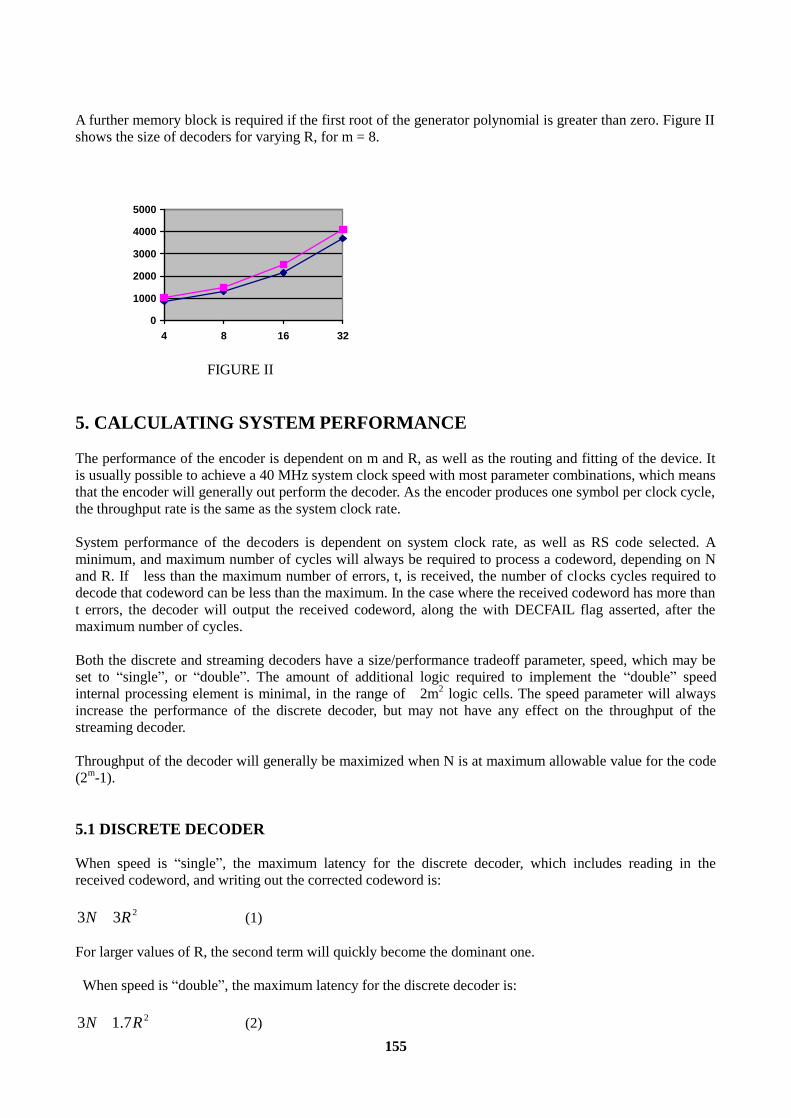
155
A further memory block is required if the first root of the generator polynomial is greater than zero. Figure II shows the size of decoders for varying R, for m = 8.
FIGURE II
5. CALCULATING SYSTEM PERFORMANCE The performance of the encoder is dependent on m and R, as well as the routing and fitting of the device. It is usually possible to achieve a 40 MHz system clock speed with most parameter combinations, which means that the encoder will generally out perform the decoder. As the encoder produces one symbol per clock cycle, the throughput rate is the same as the system clock rate. System performance of the decoders is dependent on system clock rate, as well as RS code selected. A minimum, and maximum number of cycles will always be required to process a codeword, depending on N and R. If less than the maximum number of errors, t, is received, the number of clocks cycles required to decode that codeword can be less than the maximum. In the case where the received codeword has more than t errors, the decoder will output the received codeword, along the with DECFAIL flag asserted, after the maximum number of cycles. Both the discrete and streaming decoders have a size/performance tradeoff parameter, speed, which may be set to “single”, or “double”. The amount of additional logic required to implement the “double” speed internal processing element is minimal, in the range of 2m2 logic cells. The speed parameter will always increase the performance of the discrete decoder, but may not have any effect on the throughput of the streaming decoder. Throughput of the decoder will generally be maximized when N is at maximum allowable value for the code (2m-1). 5.1 DISCRETE DECODER When speed is “single”, the maximum latency for the discrete decoder, which includes reading in the received codeword, and writing out the corrected codeword is:
233 RN + (1) For larger values of R, the second term will quickly become the dominant one. When speed is “double”, the maximum latency for the discrete decoder is:
27.13 RN + (2)
0
1000
2000
3000
4000
5000
4 8 16 32
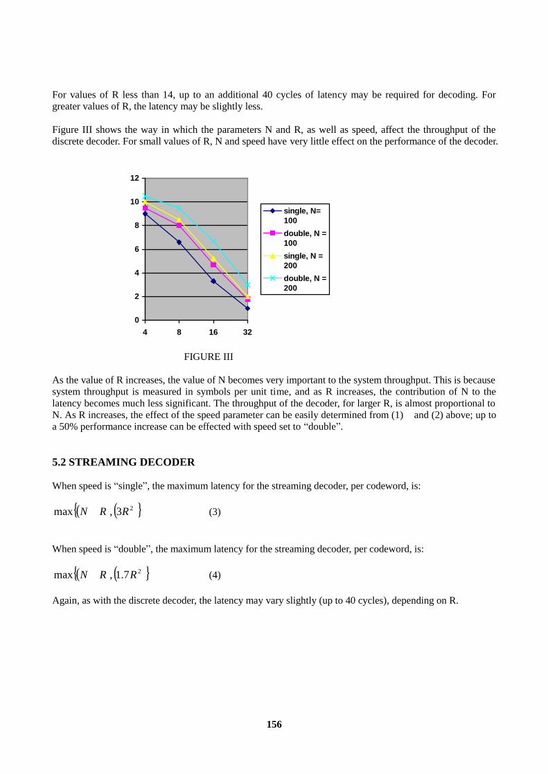
156
For values of R less than 14, up to an additional 40 cycles of latency may be required for decoding. For greater values of R, the latency may be slightly less. Figure III shows the way in which the parameters N and R, as well as speed, affect the throughput of the discrete decoder. For small values of R, N and speed have very little effect on the performance of the decoder.
FIGURE III As the value of R increases, the value of N becomes very important to the system throughput. This is because system throughput is measured in symbols per unit time, and as R increases, the contribution of N to the latency becomes much less significant. The throughput of the decoder, for larger R, is almost proportional to N. As R increases, the effect of the speed parameter can be easily determined from (1) and (2) above; up to a 50% performance increase can be effected with speed set to “double”. 5.2 STREAMING DECODER When speed is “single”, the maximum latency for the streaming decoder, per codeword, is:
( ) ( ){ }23,max RRN + (3) When speed is “double”, the maximum latency for the streaming decoder, per codeword, is:
( ) ( ){ }27.1,max RRN + (4) Again, as with the discrete decoder, the latency may vary slightly (up to 40 cycles), depending on R.
0
2
4
6
8
10
12
4 8 16 32
single, N=100double, N =100single, N =200double, N =200
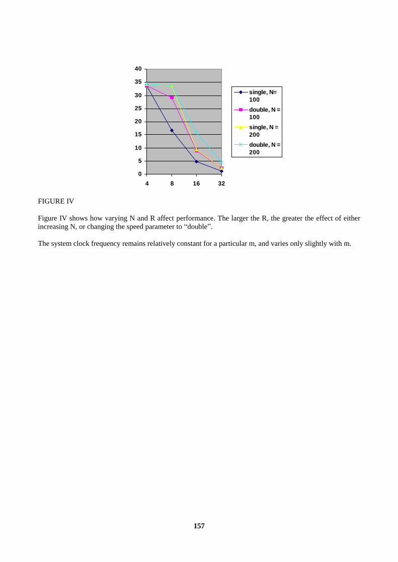
157
FIGURE IV Figure IV shows how varying N and R affect performance. The larger the R, the greater the effect of either increasing N, or changing the speed parameter to “double”. The system clock frequency remains relatively constant for a particular m, and varies only slightly with m.
0
5
10
15
20
25
30
35
40
4 8 16 32
single, N=100double, N =100single, N =200double, N =200

158
CONCLUSIONS
High performance Reed Solomon encoders and decoders can easily be designed with fully parameterized design tools. These Reed Solomon cores can then be synthesized into programmable logic, resulting in the same order, or higher performance, than standard (ASSP) devices. Given the RS parameters, core size and performance can readily be estimated, prior to synthesis. REFERENCES
1. S.B. Wicker, V.K. Bhargava, editors, Reed-Solomon Codes and their Applications, IEEE Press, New
York, 1994 2. “Hammer Cores Reed Solomon Encoders and Decoders Data Sheet”, HammerCores,
www.hammercores.com