Embed Size (px)
Citation preview

ALTIUMLIVE 2018:UNLEASH THE POWER AND POTENTIAL OF ALTIUM’S DESIGN RULE CAPABILITIESKelly WigingtonDirector of PCB Design,VPI Technology Group
San DiegoOctober 4, 2018
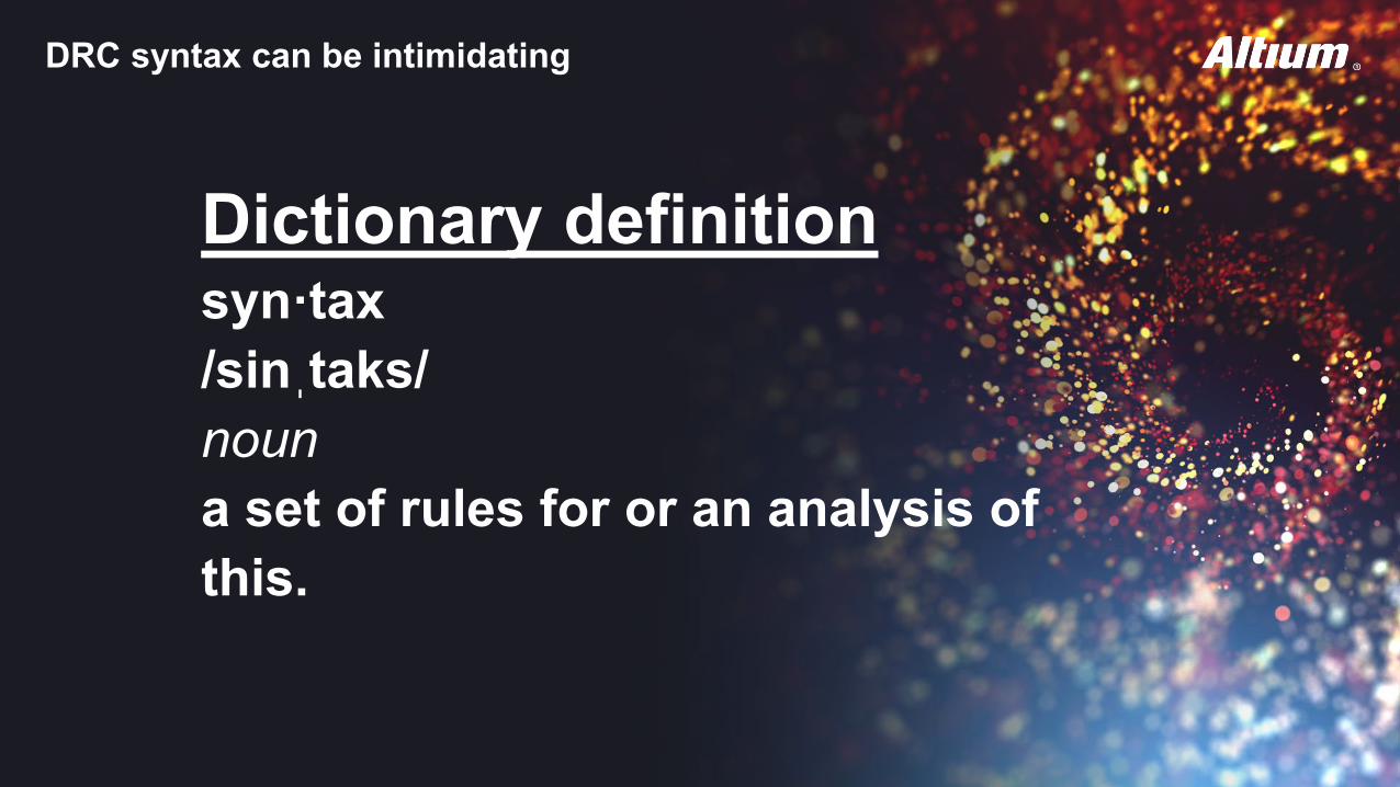
Dictionary definitionsyn·tax/sinˌtaks/nouna set of rules for or an analysis of this.
DRC syntax can be intimidating
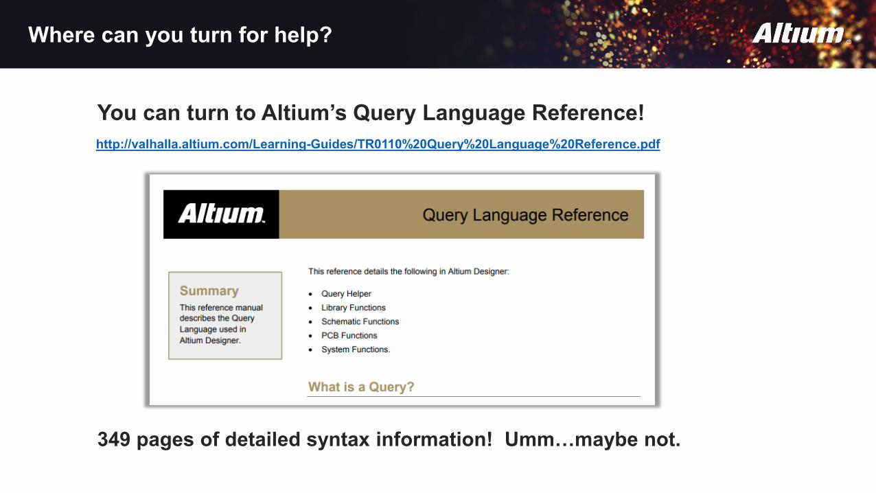
Where can you turn for help?
You can turn to Altium’s Query Language Reference!
349 pages of detailed syntax information! Umm…maybe not.
http://valhalla.altium.com/Learning-Guides/TR0110%20Query%20Language%20Reference.pdf
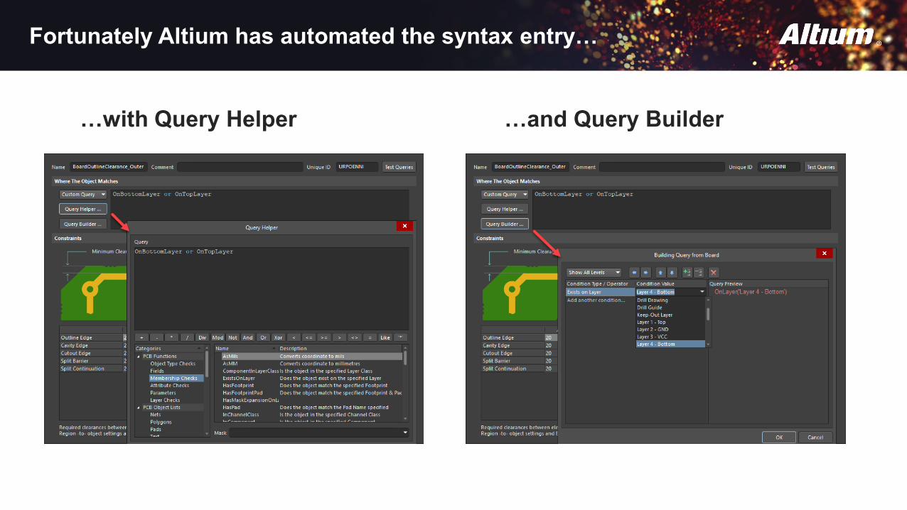
Fortunately Altium has automated the syntax entry…
…with Query Helper …and Query Builder
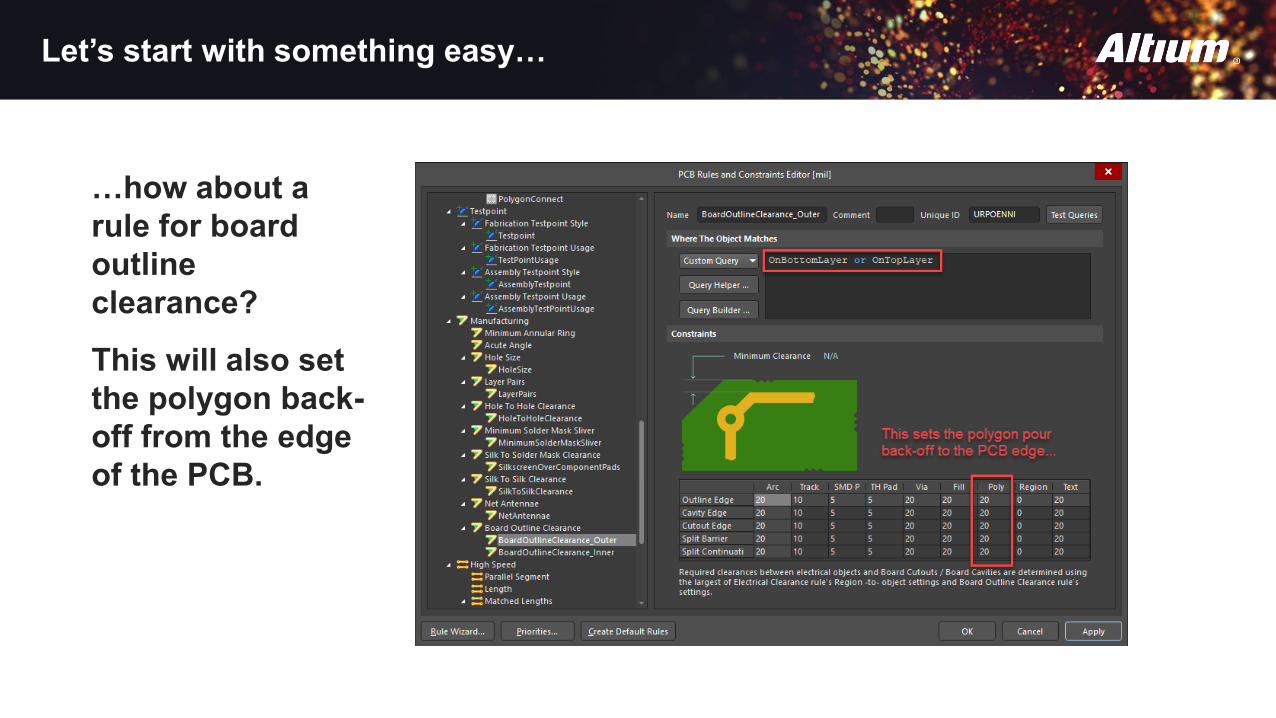
Let’s start with something easy…
…how about a rule for board outline clearance?
This will also set the polygon back-off from the edge of the PCB.
Let’s start with something easy…
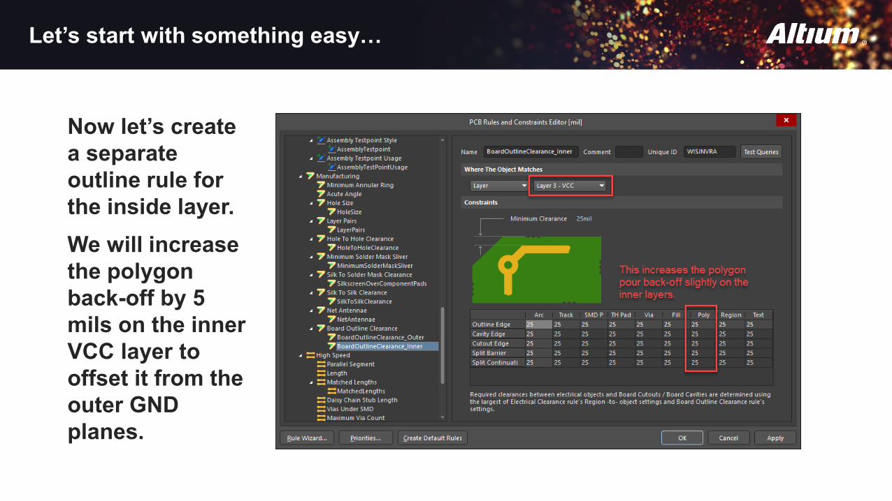
Now let’s create a separate outline rule for the inside layer. We will increase the polygon back-off by 5 mils on the inner VCC layer to offset it from the outer GND planes.
Let’s start with something easy…
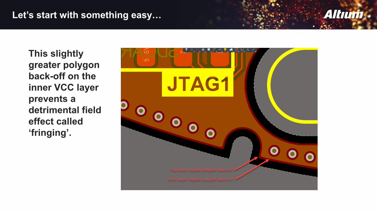
This slightly greater polygon back-off on the inner VCC layer prevents a detrimental field effect called ‘fringing’.
Let’s start with something easy…
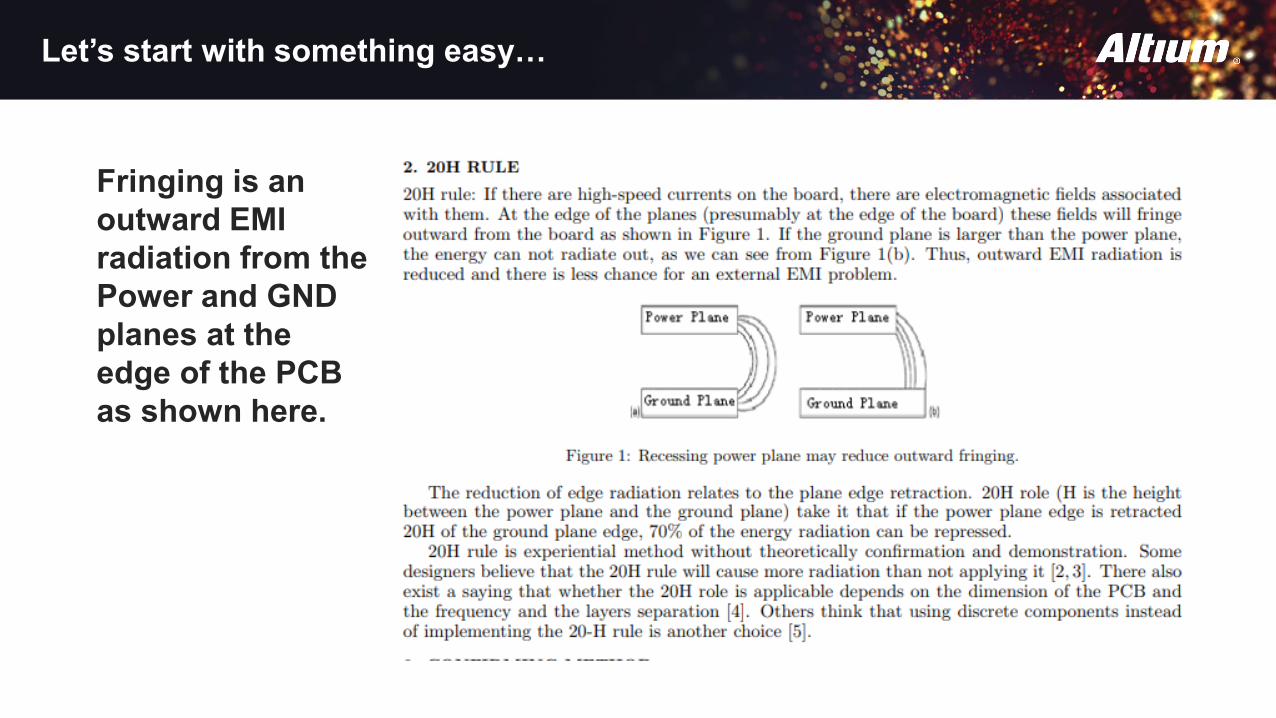
Fringing is an outward EMI radiation from the Power and GND planes at the edge of the PCB as shown here.
While on the subject of polygons…
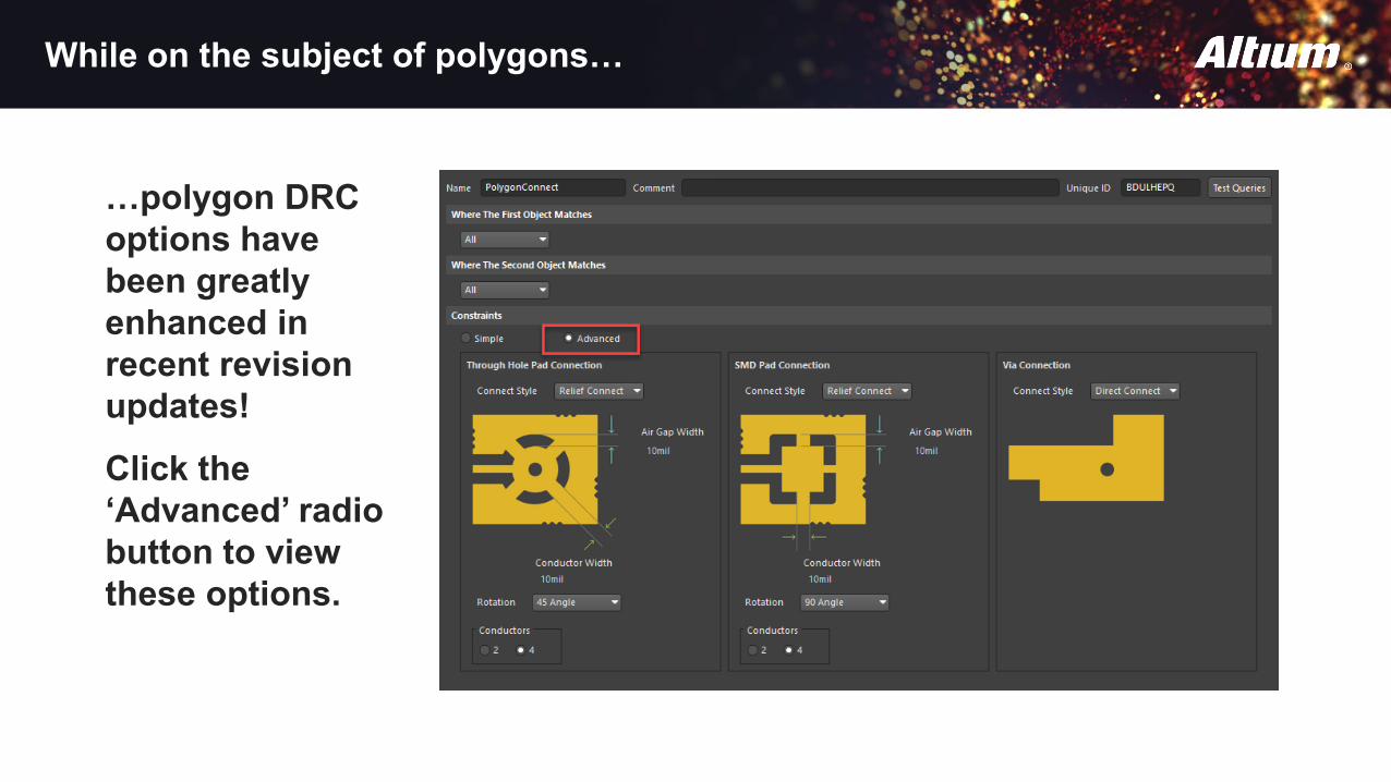
…polygon DRC options have been greatly enhanced in recent revision updates!
Click the ‘Advanced’ radio button to view these options.
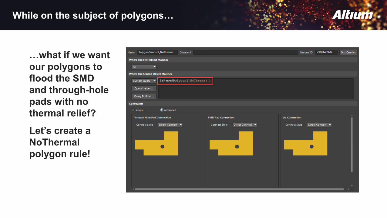
While on the subject of polygons…
…what if we want our polygons to flood the SMD and through-hole pads with no thermal relief?
Let’s create a NoThermalpolygon rule!
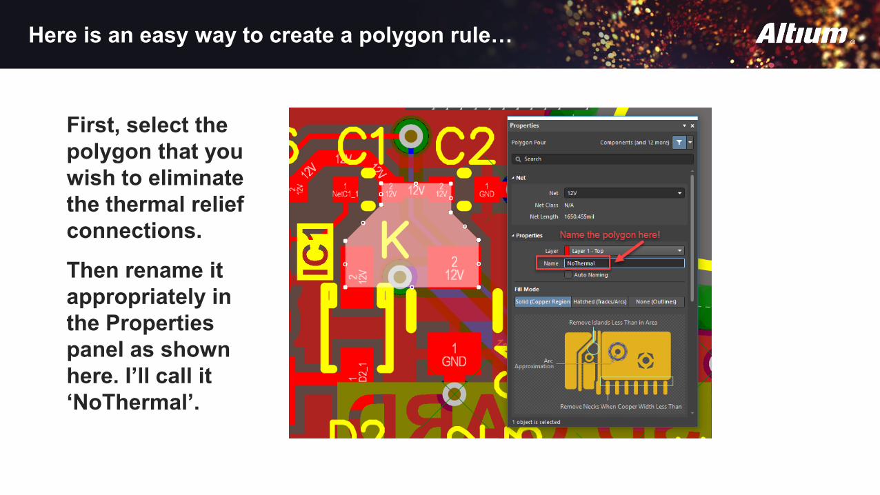
Here is an easy way to create a polygon rule…
First, select the polygon that you wish to eliminate the thermal relief connections.
Then rename it appropriately in the Properties panel as shown here. I’ll call it ‘NoThermal’.
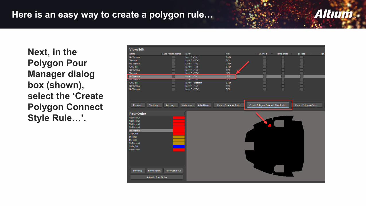
Here is an easy way to create a polygon rule…
Next, in the Polygon Pour Manager dialog box (shown), select the ‘Create Polygon Connect Style Rule…’.
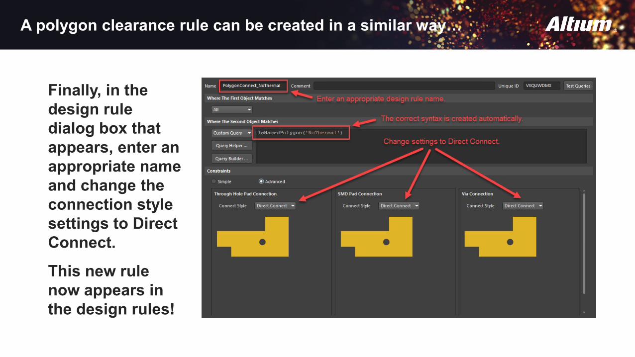
A polygon clearance rule can be created in a similar way…
Finally, in the design rule dialog box that appears, enter an appropriate name and change the connection style settings to Direct Connect.
This new rule now appears in the design rules!
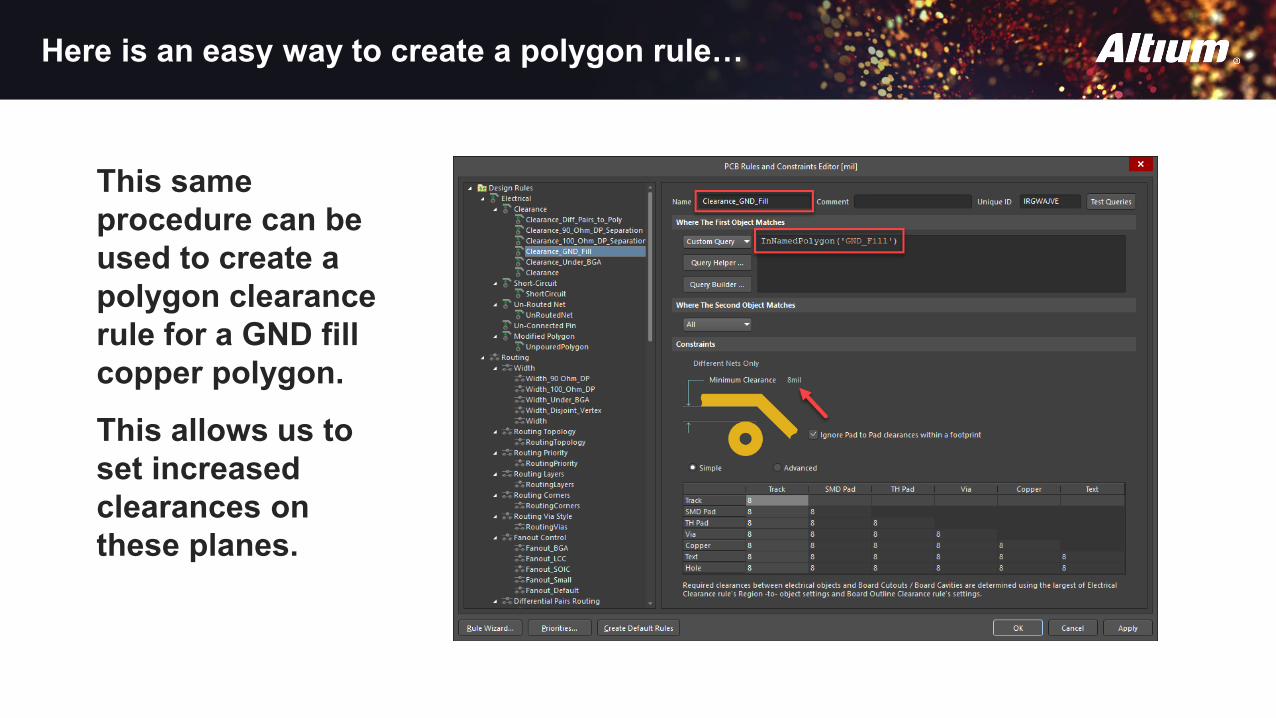
Here is an easy way to create a polygon rule…
This same procedure can be used to create a polygon clearance rule for a GND fill copper polygon.
This allows us to set increased clearances on these planes.
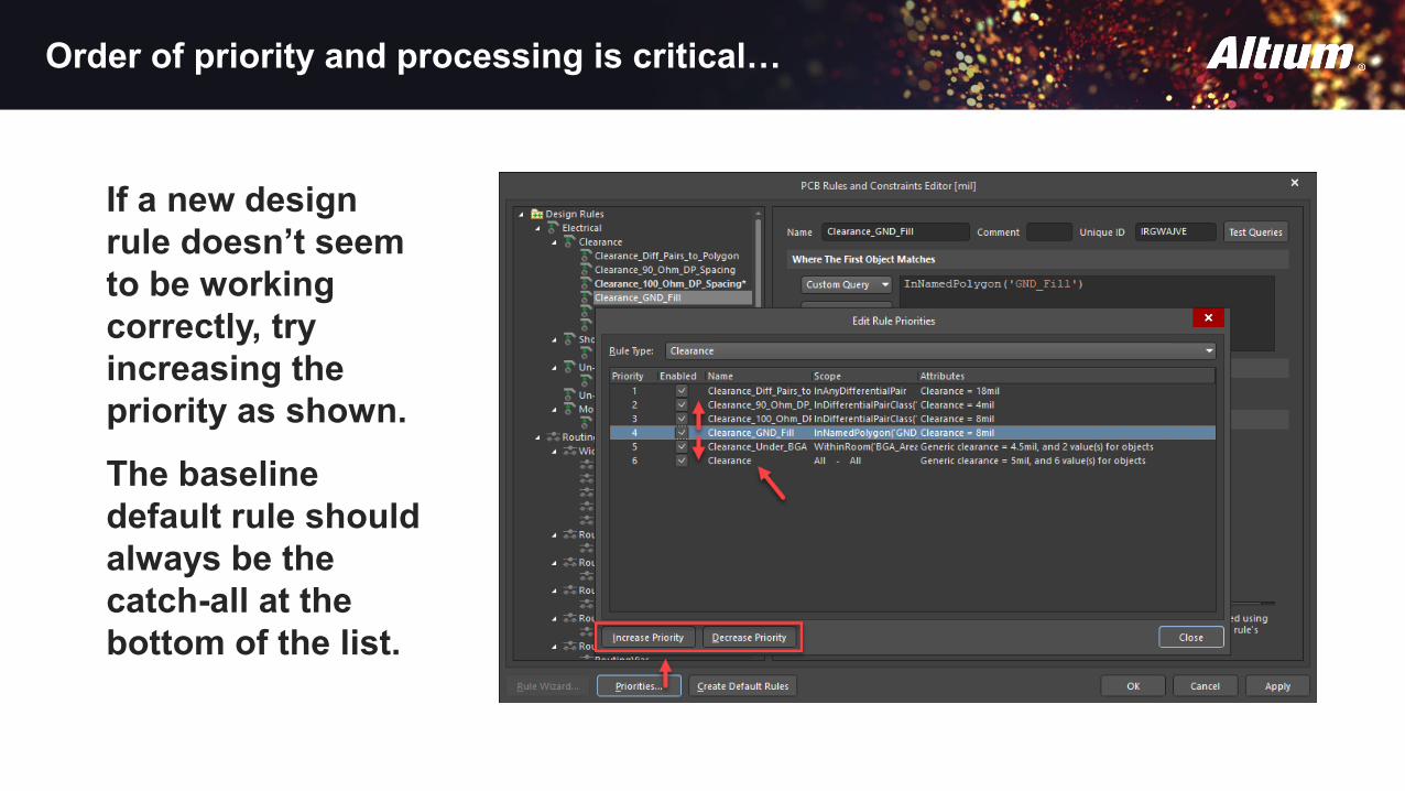
Order of priority and processing is critical…
If a new design rule doesn’t seem to be working correctly, try increasing the priority as shown.
The baseline default rule should always be the catch-all at the bottom of the list.
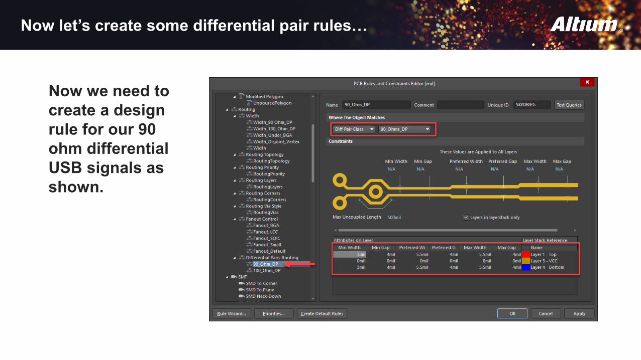
Now let’s create some differential pair rules…
Now we need to create a design rule for our 90 ohm differential USB signals as shown.
Now let’s create some differential pair rules…
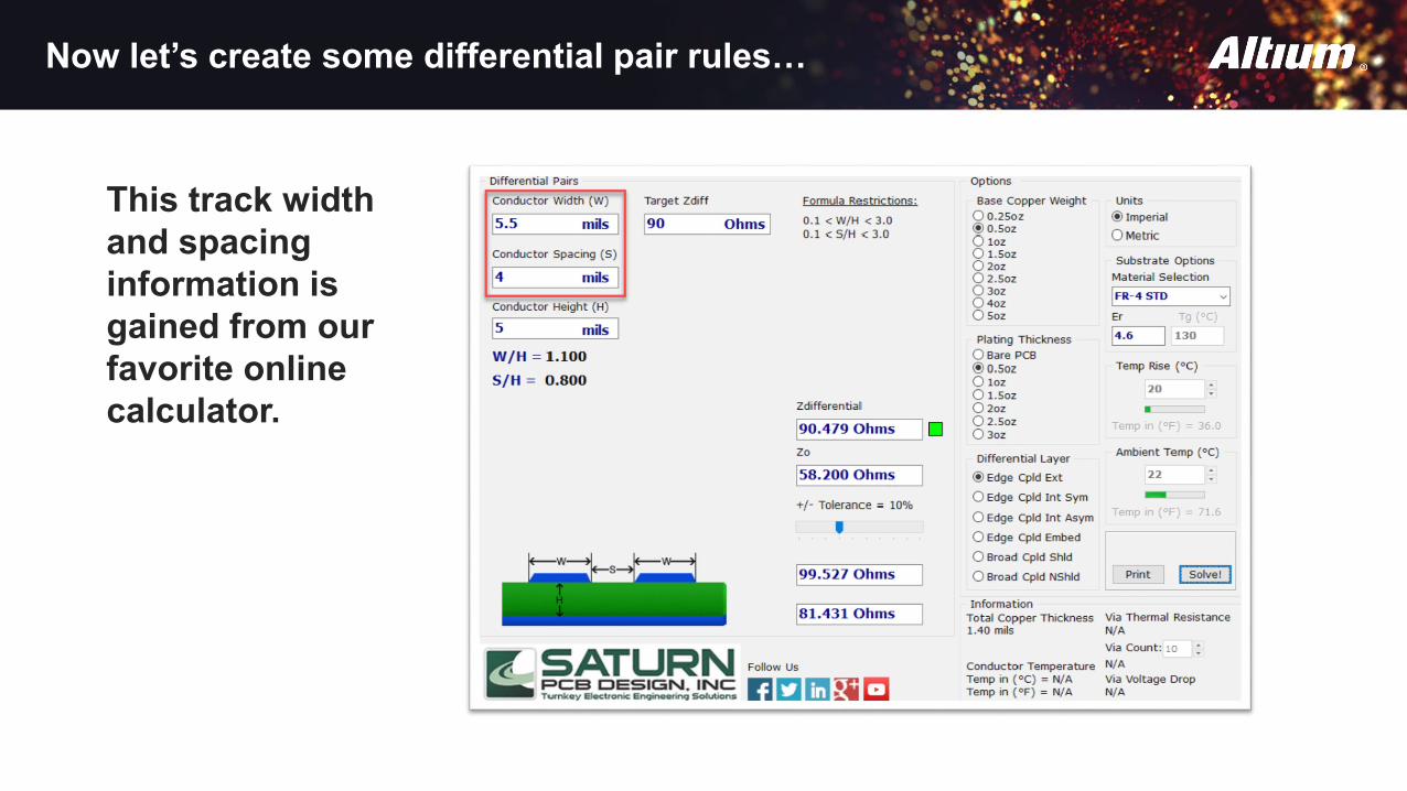
This track width and spacing information is gained from our favorite online calculator.
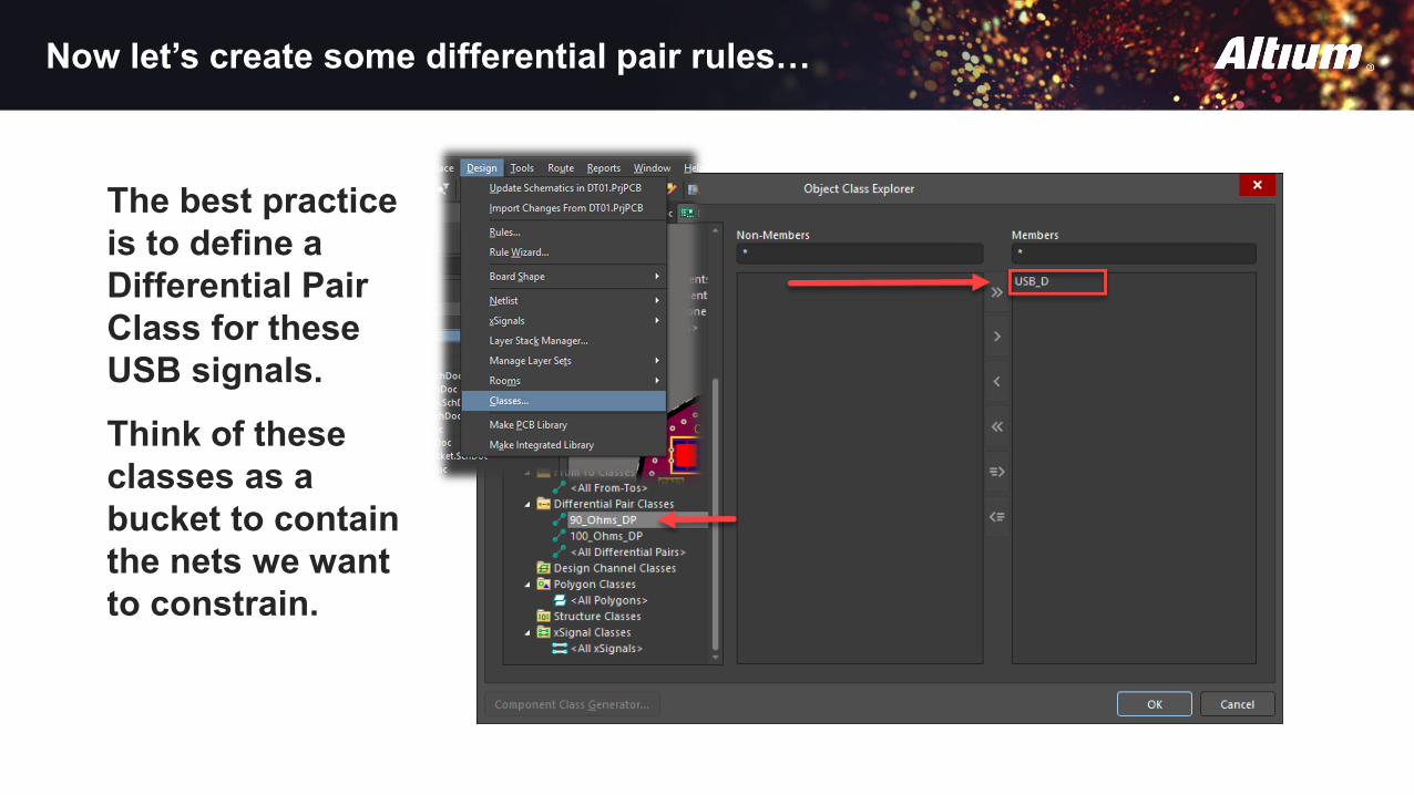
Now let’s create some differential pair rules…
The best practice is to define a Differential Pair Class for these USB signals.
Think of these classes as a bucket to contain the nets we want to constrain.
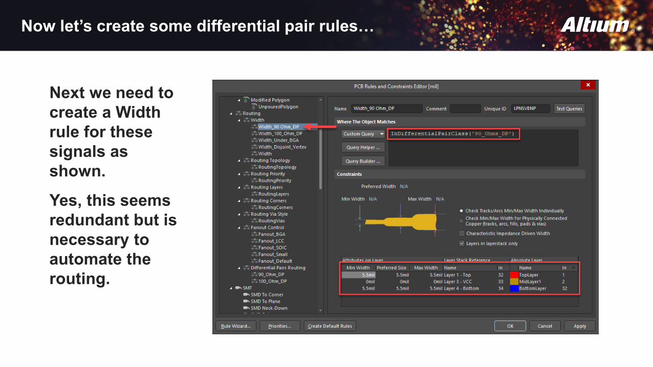
Now let’s create some differential pair rules…
Next we need to create a Width rule for these signals as shown.
Yes, this seems redundant but is necessary to automate the routing.
Now let’s create some differential pair rules…
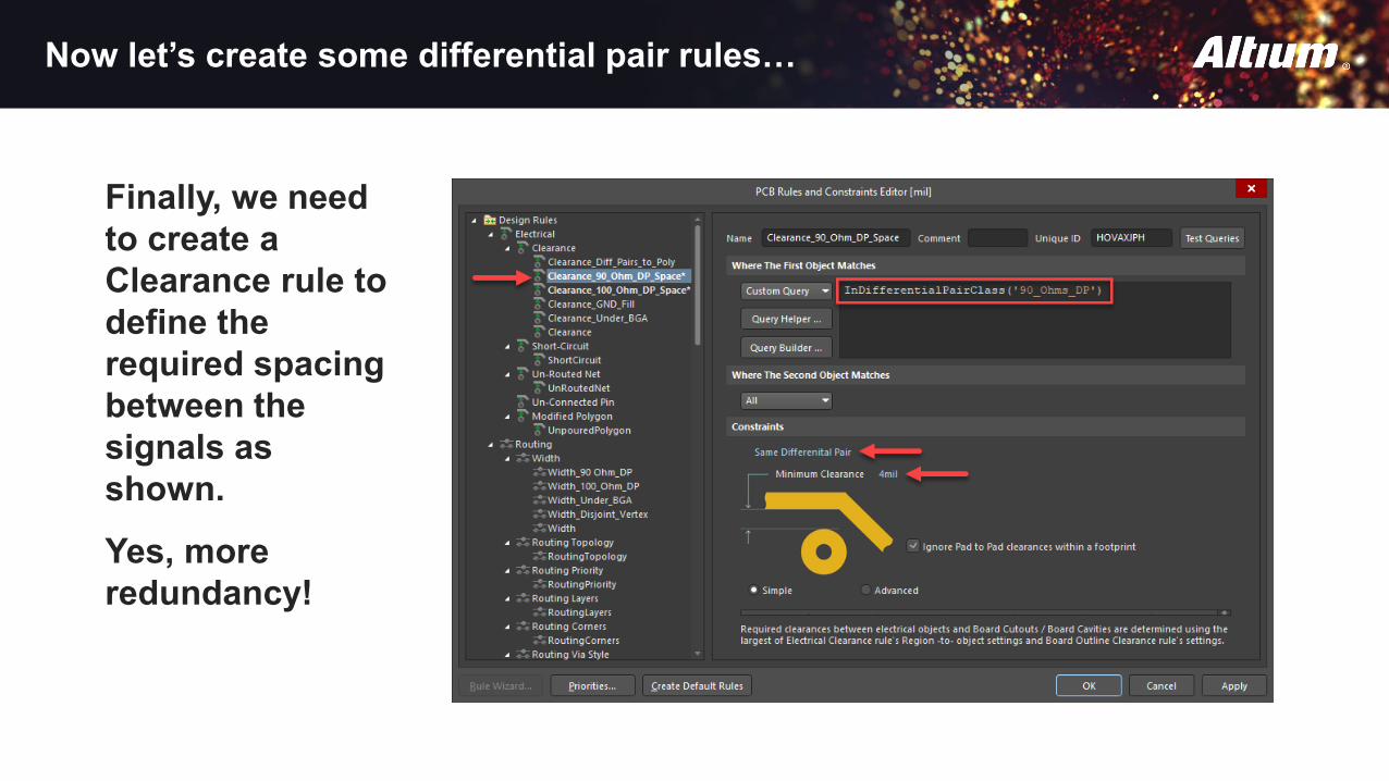
Finally, we need to create a Clearance rule to define the required spacing between the signals as shown.
Yes, more redundancy!
The BIG payoff…
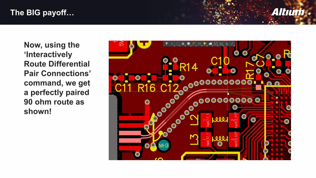
Now, using the ‘Interactively Route Differential Pair Connections’ command, we get a perfectly paired 90 ohm route as shown!
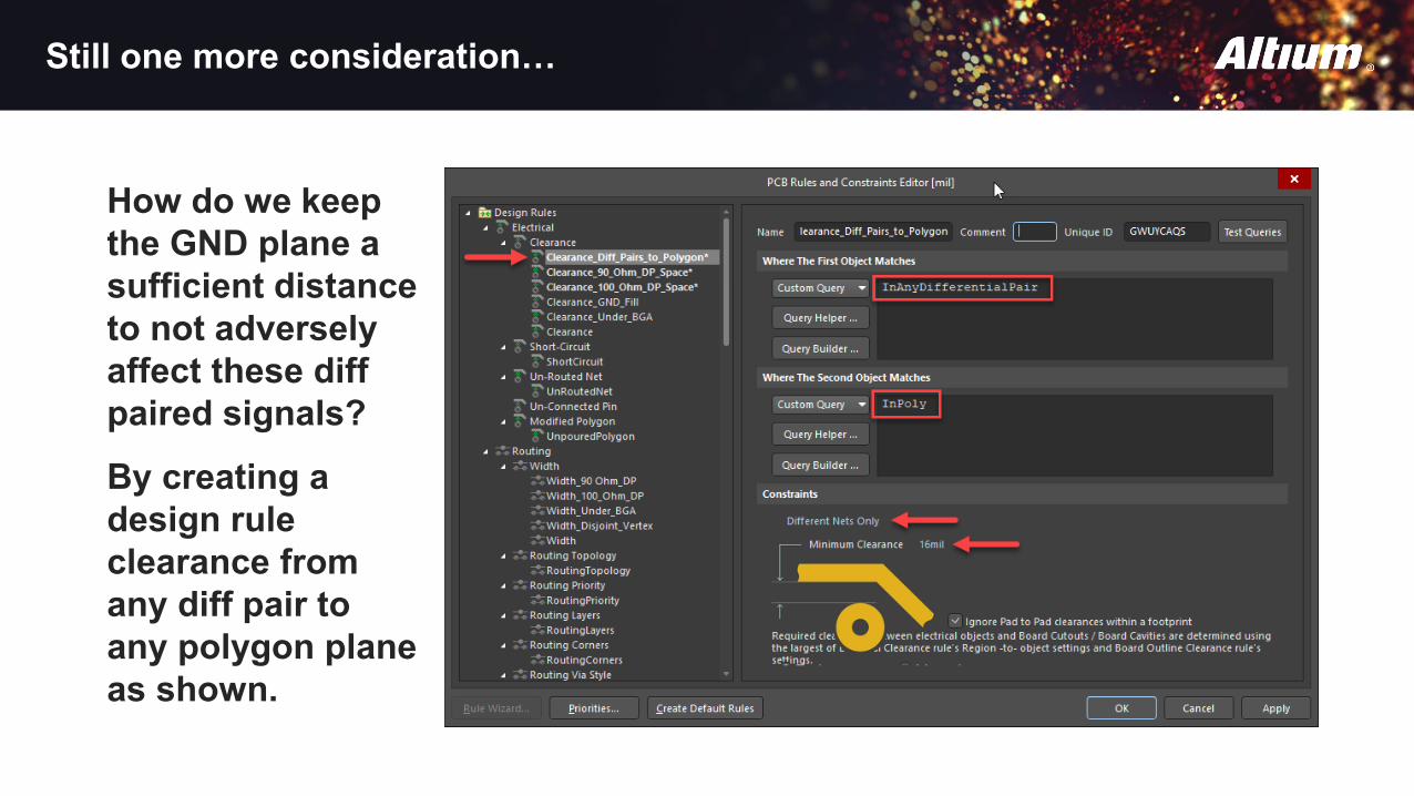
Still one more consideration…
How do we keep the GND plane a sufficient distance to not adversely affect these diff paired signals?
By creating a design rule clearance from any diff pair to any polygon plane as shown.
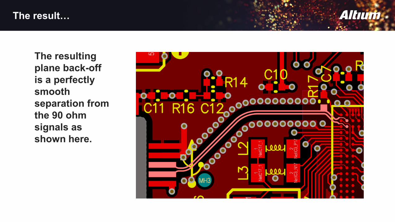
The result…
The resulting plane back-off is a perfectly smooth separation from the 90 ohm signals as shown here.
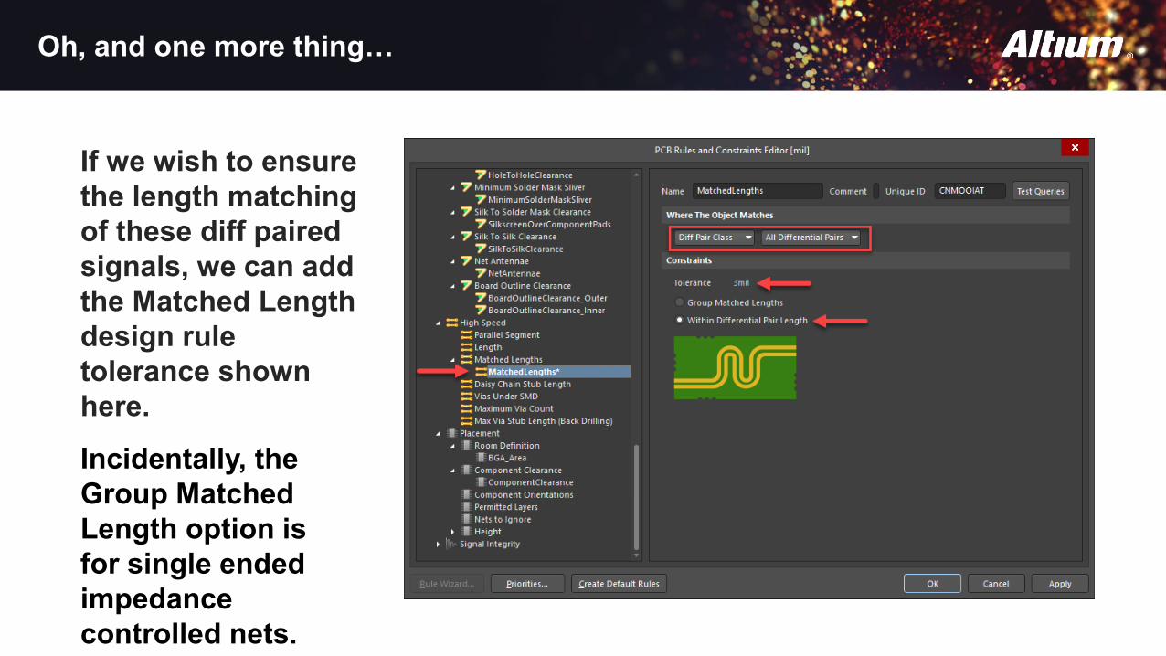
Oh, and one more thing…
If we wish to ensure the length matching of these diff paired signals, we can add the Matched Length design rule tolerance shown here.
Incidentally, the Group Matched Length option is for single ended impedance controlled nets.
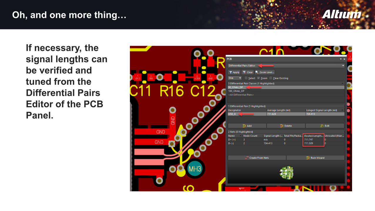
Oh, and one more thing…
If necessary, the signal lengths can be verified and tuned from the Differential Pairs Editor of the PCB Panel.
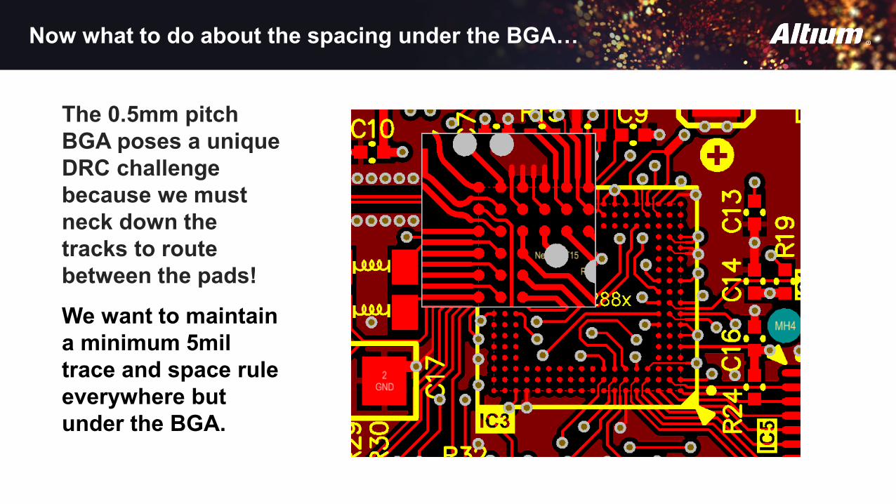
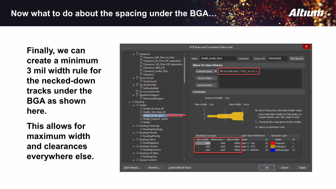
Now what to do about the spacing under the BGA…
The 0.5mm pitch BGA poses a unique DRC challenge because we must neck down the tracks to route between the pads!
We want to maintain a minimum 5mil trace and space rule everywhere but under the BGA.
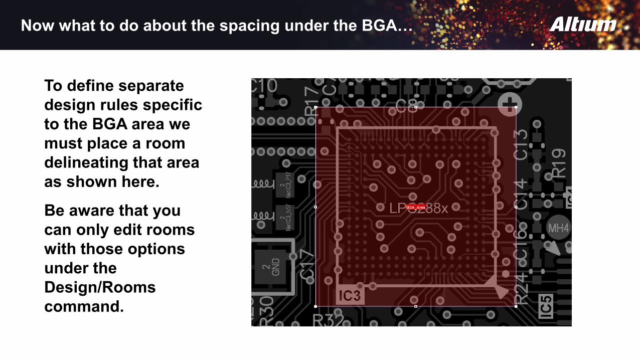
Now what to do about the spacing under the BGA…
To define separate design rules specific to the BGA area we must place a room delineating that area as shown here.
Be aware that you can only edit rooms with those options under the Design/Rooms command.
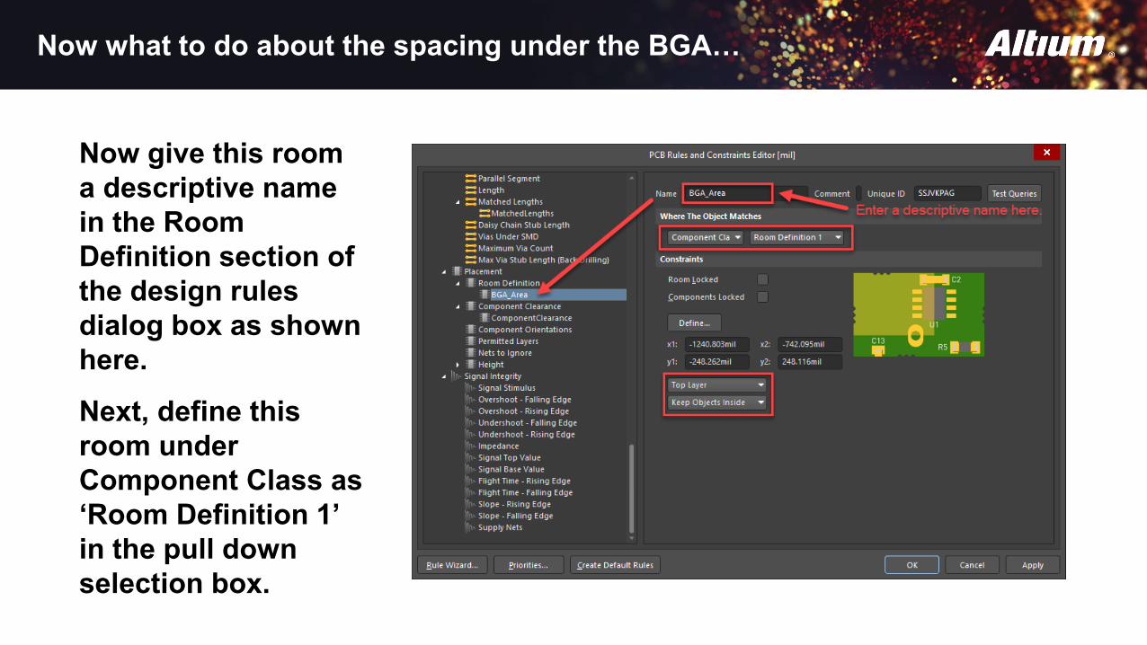
Now what to do about the spacing under the BGA…
Now give this room a descriptive name in the Room Definition section of the design rules dialog box as shown here.
Next, define this room under Component Class as ‘Room Definition 1’ in the pull down selection box.
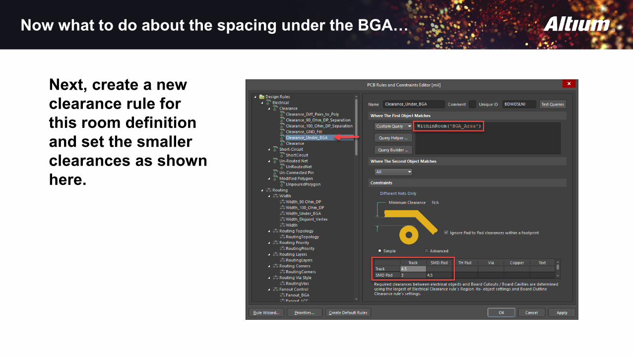
Now what to do about the spacing under the BGA…
Next, create a new clearance rule for this room definition and set the smaller clearances as shown here.
Now what to do about the spacing under the BGA…
Finally, we can create a minimum 3 mil width rule for the necked-down tracks under the BGA as shown here.
This allows for maximum width and clearances everywhere else.
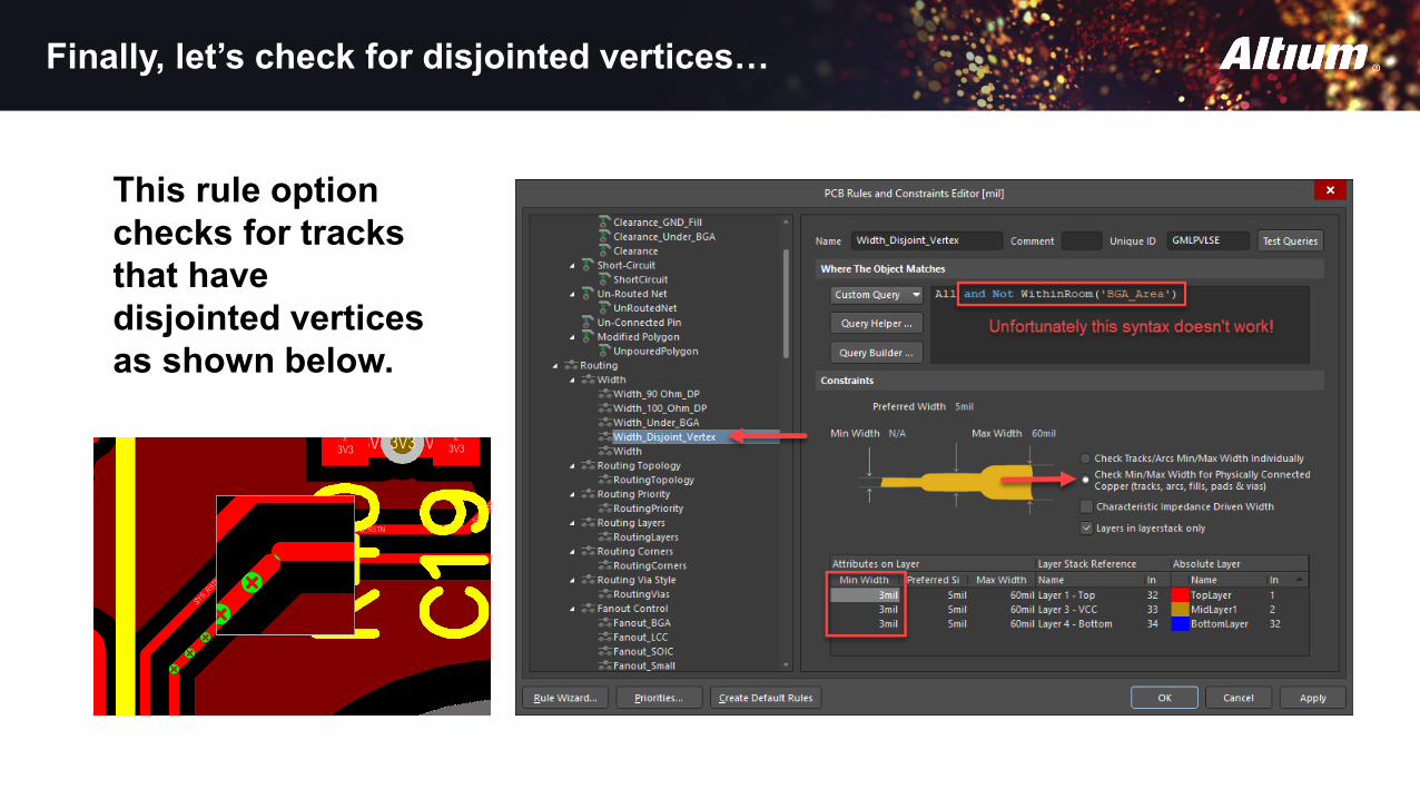
Finally, let’s check for disjointed vertices…
This rule option checks for tracks that have disjointed vertices as shown below.
Well, this is great information, but…
…how do I integrate these rules into my PCB as needed and applicable?
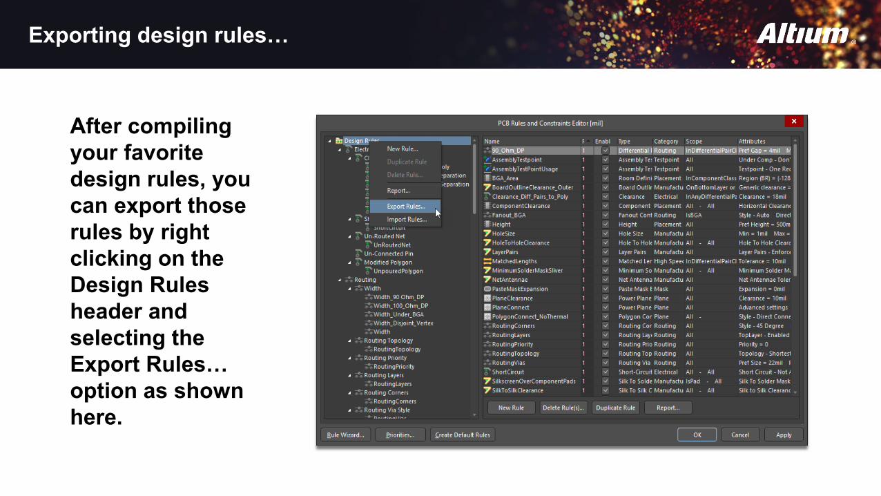
Exporting design rules…
After compiling your favorite design rules, you can export those rules by right clicking on the Design Rules header and selecting the Export Rules… option as shown here.
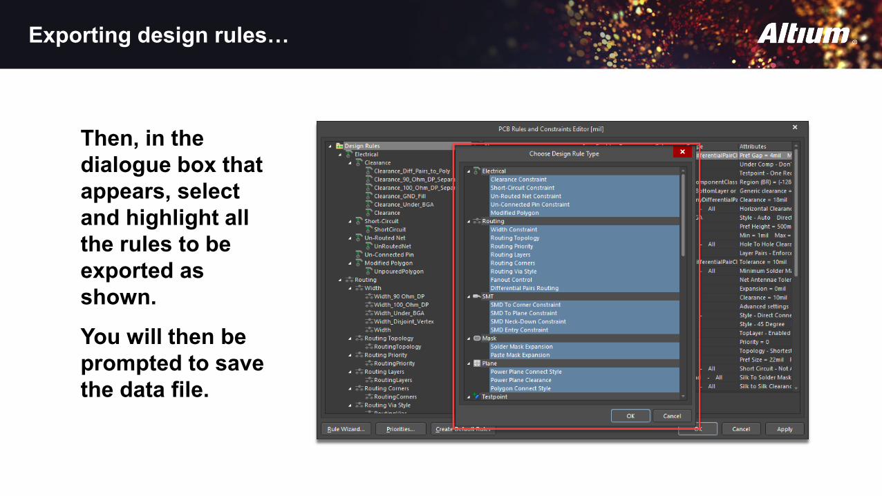
Exporting design rules…
Then, in the dialogue box that appears, select and highlight all the rules to be exported as shown.
You will then be prompted to save the data file.
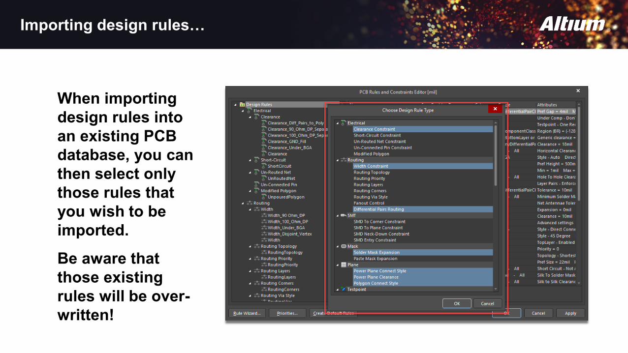
Importing design rules…
When importing design rules into an existing PCB database, you can then select only those rules that you wish to be imported.
Be aware that those existing rules will be over-written!
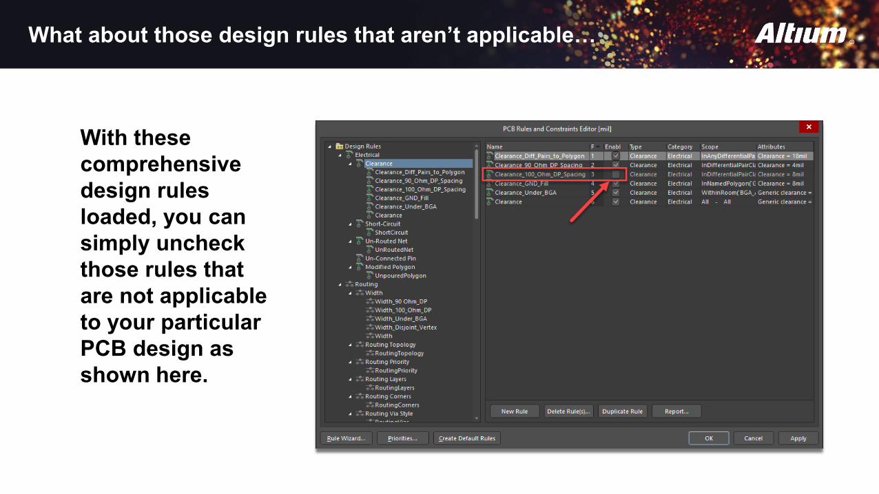
What about those design rules that aren’t applicable…
With these comprehensive design rules loaded, you can simply uncheck those rules that are not applicable to your particular PCB design as shown here.
One more bonus tip…
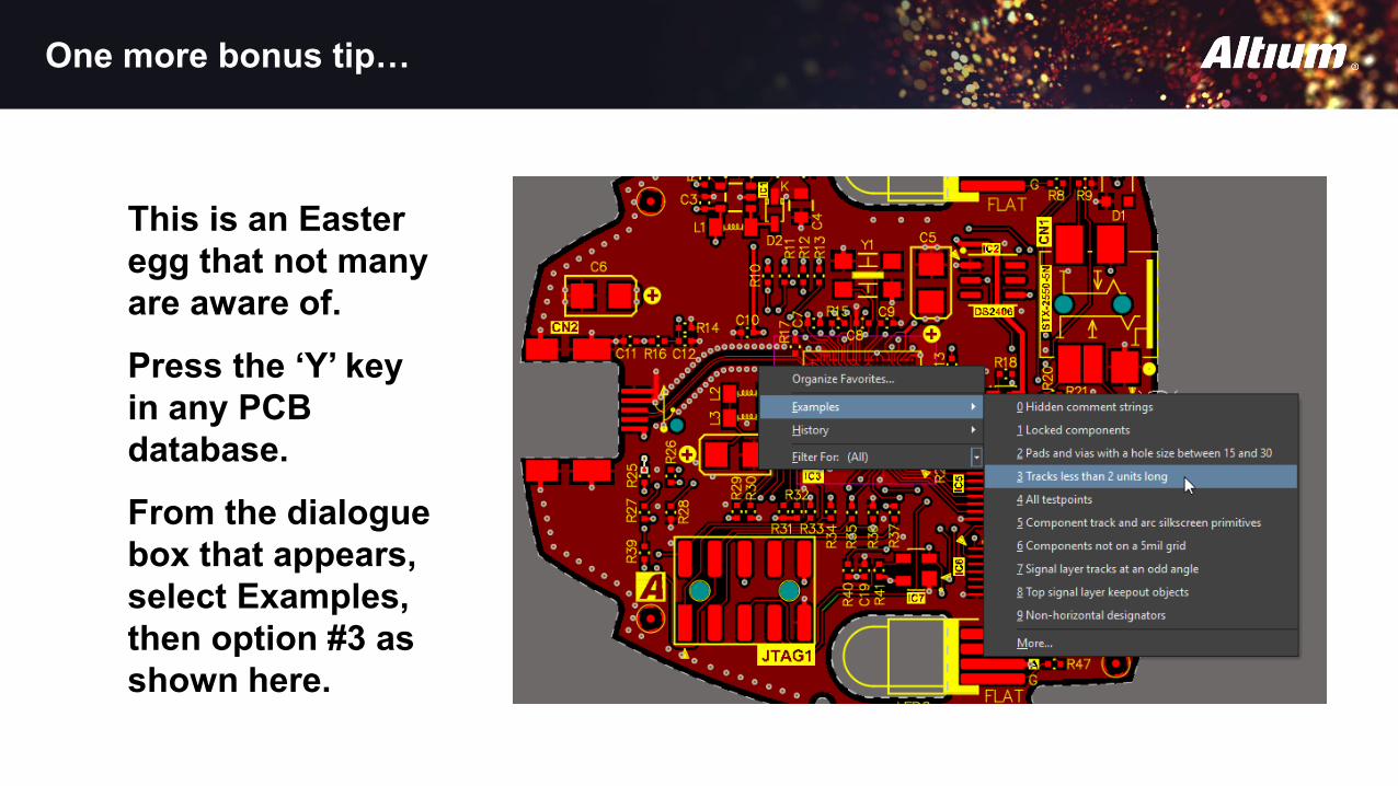
This is an Easter egg that not many are aware of.
Press the ‘Y’ key in any PCB database.
From the dialogue box that appears, select Examples, then option #3 as shown here.
One more bonus tip…
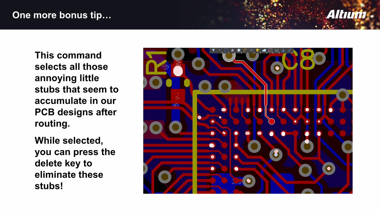
This command selects all those annoying little stubs that seem to accumulate in our PCB designs after routing.
While selected, you can press the delete key to eliminate these stubs!
One more bonus tip…
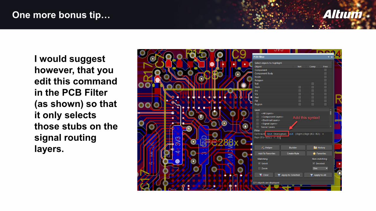
I would suggest however, that you edit this command in the PCB Filter (as shown) so that it only selects those stubs on the signal routing layers.
One more bonus tip…
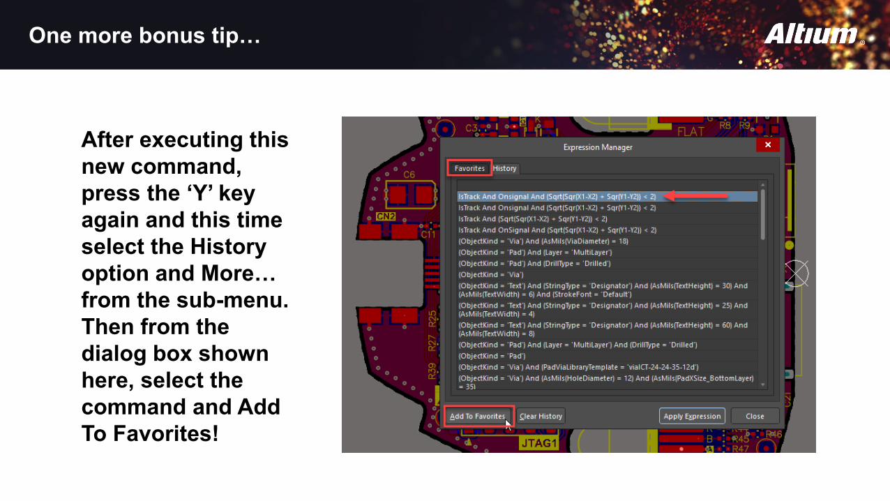
After executing this new command, press the ‘Y’ key again and this time select the History option and More… from the sub-menu. Then from the dialog box shown here, select the command and Add To Favorites!
One more bonus tip…
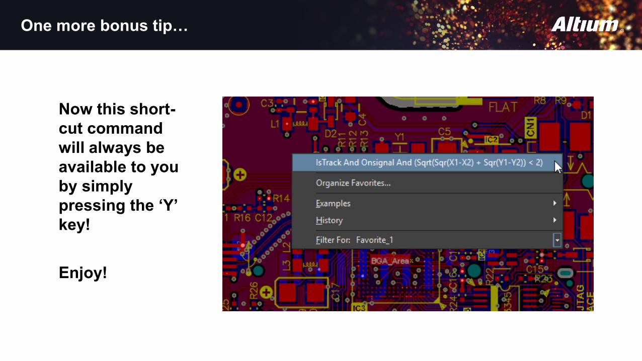
Now this short-cut command will always be available to you by simply pressing the ‘Y’ key!
Enjoy!

May all your PCBs be error free!
Kelly Wigington, CID+
Director of PCB Design,VPI Technology Group [email protected]
Email me if you would like a copy of my design rule file or this slide deck.