Embed Size (px)
Citation preview
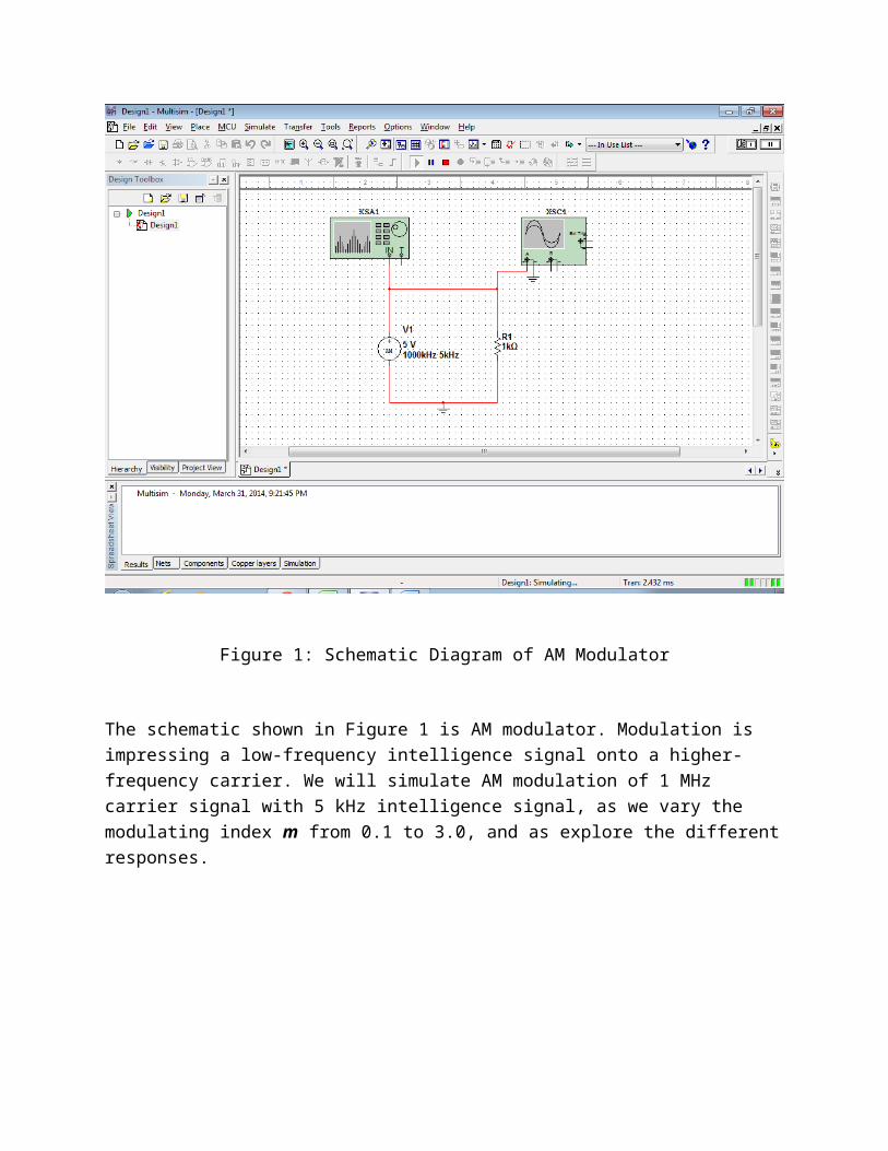
Figure 1: Schematic Diagram of AM Modulator
The schematic shown in Figure 1 is AM modulator. Modulation is impressing a low-frequency intelligence signal onto a higher-frequency carrier. We will simulate AM modulation of 1 MHz carrier signal with 5 kHz intelligence signal, as we vary the modulating index m from 0.1 to 3.0, and as explore the different responses.

Figure 2: Time Domain Waveform of AM Modulation with m=0.1
Our first AM sample is shown on Figure 2. The modulating index is set to 0.1 and we have small change in amplitude. As you can see on Figure 4, 6, 8, 10, 12, 14, 16, 18 & 20 the higher the modulation index the higher the envelope amplitude.
Figure 3: Frequency Domain Waveform of AM Modulation with m=0.1
On Figure 3 is shown the upper sideband, lower sideband and the center frequency amplitudes. The upper sideband and the lower sideband are with approximately the same amplitudes (0.1V). But us we increase the modulation index the upper sideband and the lower sideband increase.
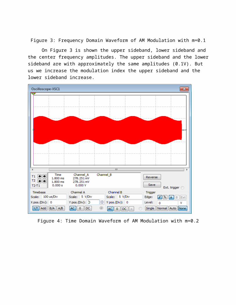
Figure 4: Time Domain Waveform of AM Modulation with m=0.2
Figure 5: Frequency Domain Waveform of AM Modulation with m=0.2
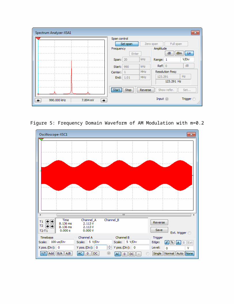
Figure 6: Time Domain Waveform of AM Modulation with m=0.3
Figure 7: Frequency Domain Waveform of AM Modulation with m=0.3
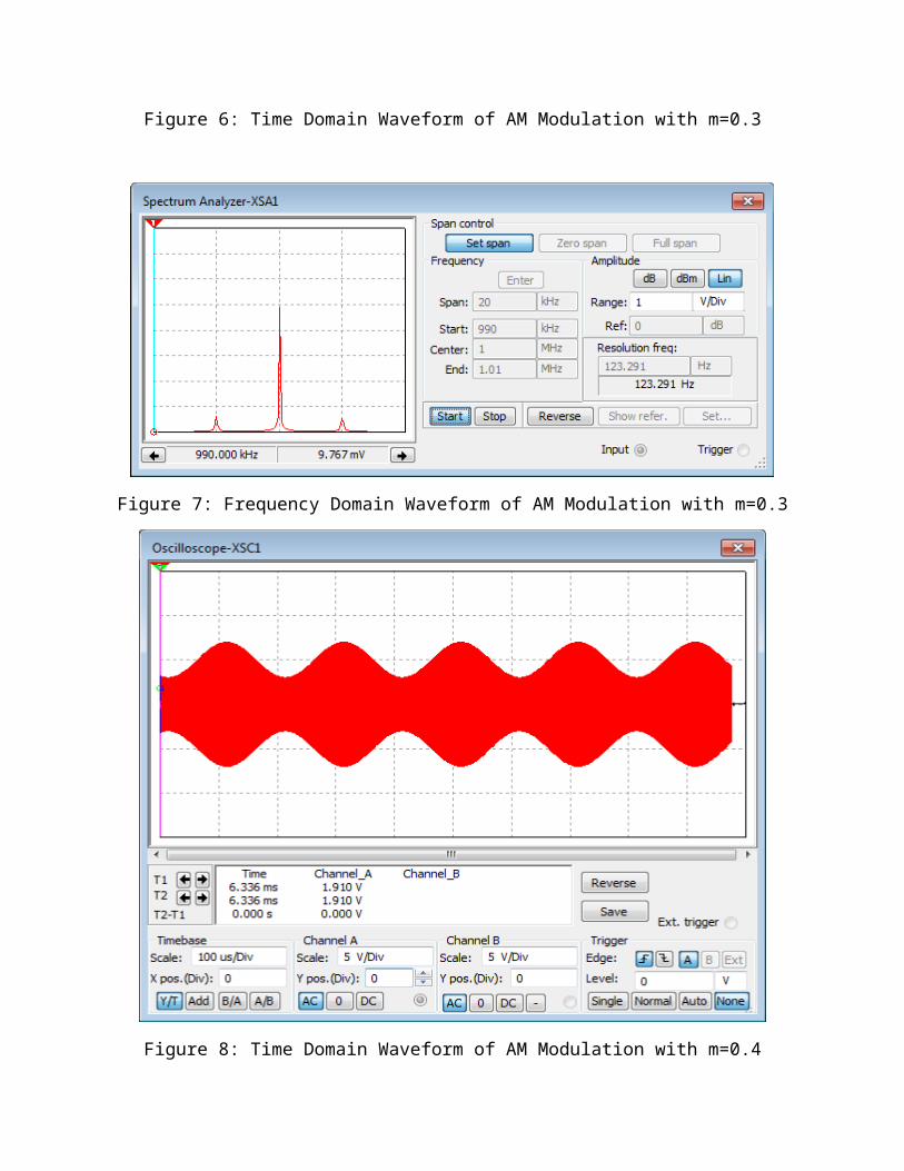
Figure 8: Time Domain Waveform of AM Modulation with m=0.4
Figure 9: Frequency Domain Waveform of AM Modulation with m=0.4
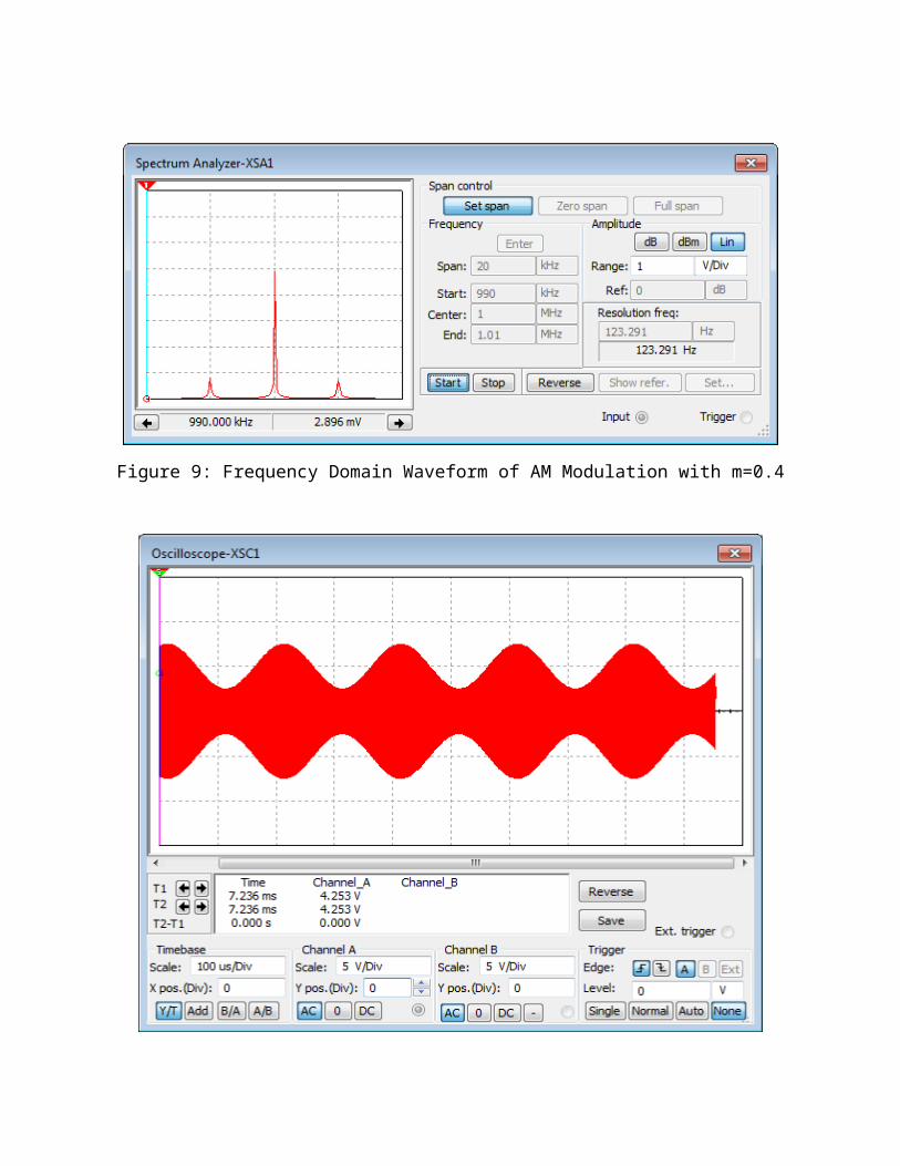
Figure 10: Time Domain Waveform of AM Modulation with m=0.5
Figure 11: Frequency Domain Waveform of AM Modulation with m=0.5
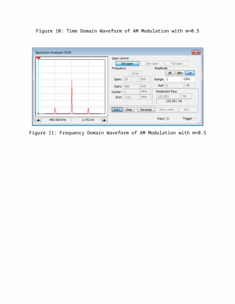
Figure 12: Time Domain Waveform of AM Modulation with m=0.6
Figure 13: Frequency Domain Waveform of AM Modulation with m=0.6
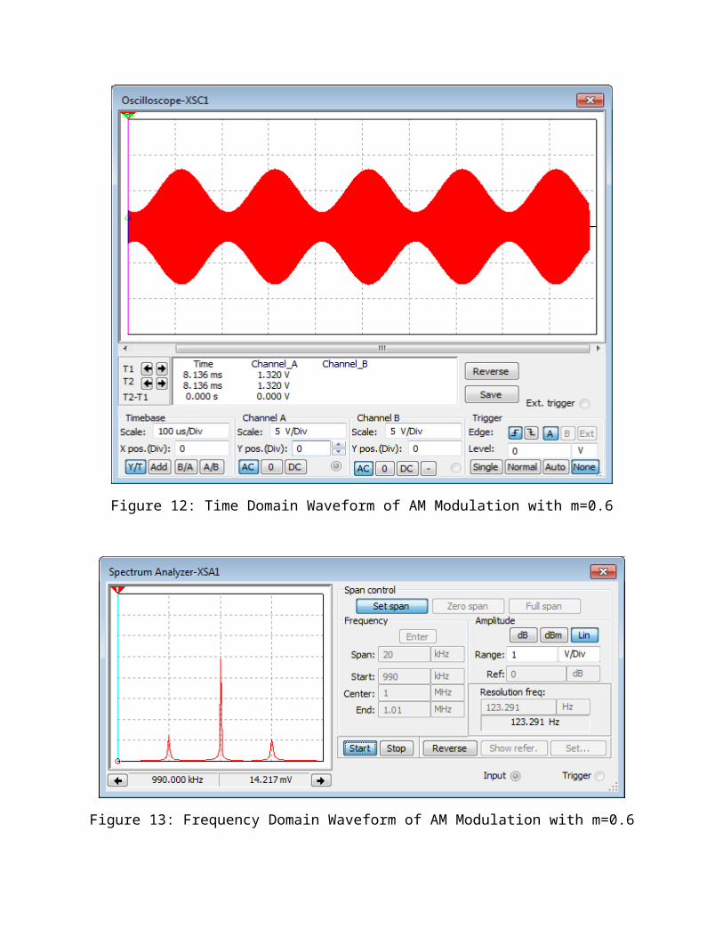
Figure 14: Time Domain Waveform of AM Modulation with m=0.7
Figure 15: Frequency Domain Waveform of AM Modulation with m=0.7
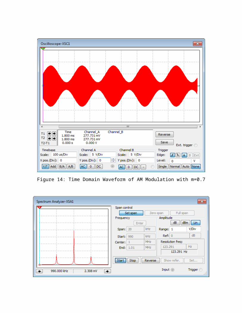
Figure 16: Time Domain Waveform of AM Modulation with m=0.8
Figure 17: Frequency Domain Waveform of AM Modulation with m=0.8
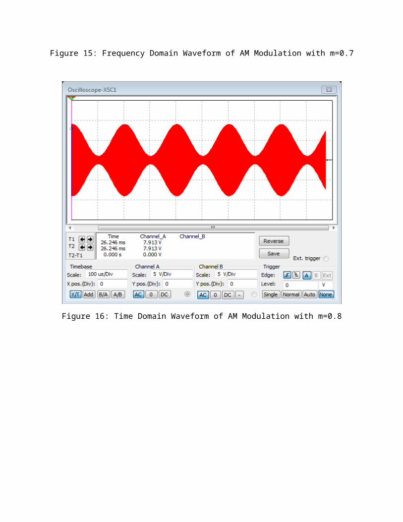
Figure 18: Time Domain Waveform of AM Modulation with m=0.9
Figure 19: Frequency Domain Waveform of AM Modulation with m=0.9
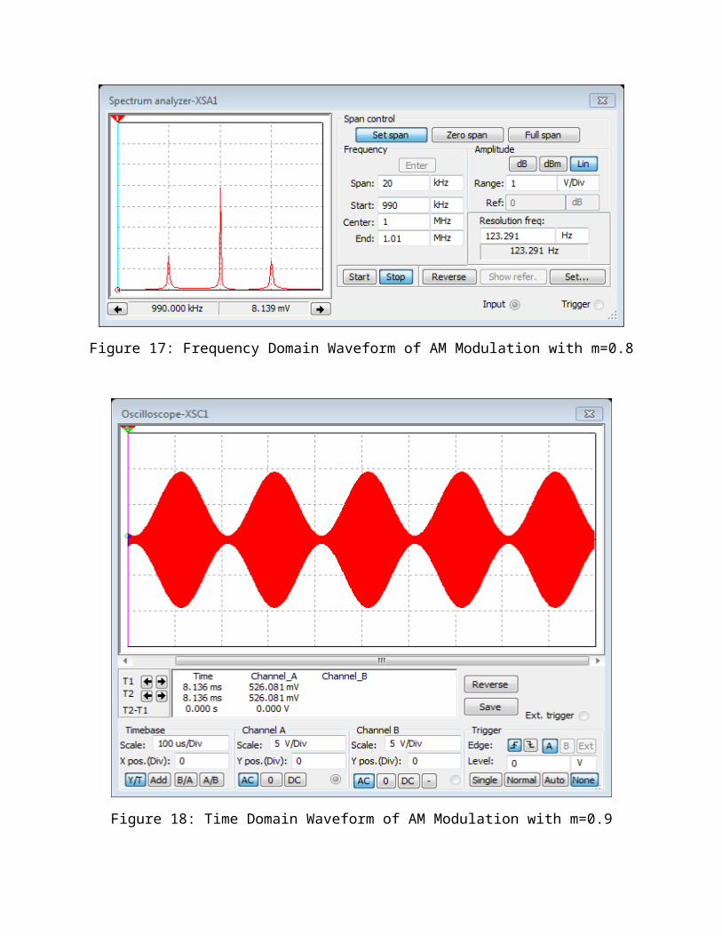
Figure 20 shows the AM modulation with modulation index of 1.0. For us this is the end of the line. As you see the upper and the lower envelops are touching. If we go any further we will go into over-modulation, which is bad because our upper and lower envelopes will overlap.
Figure 21: Frequency Domain Waveform of AM Modulation with m=1.0
Figure 21 shows AM modulation with modulation index 1.0. As you see the upper sideband is at 1.8V and the lower sideband is at 2.1V. On calculations these should be the same but in practice they are different. The reason is because we are combining the carrier and the intelligence through a non-linear device.
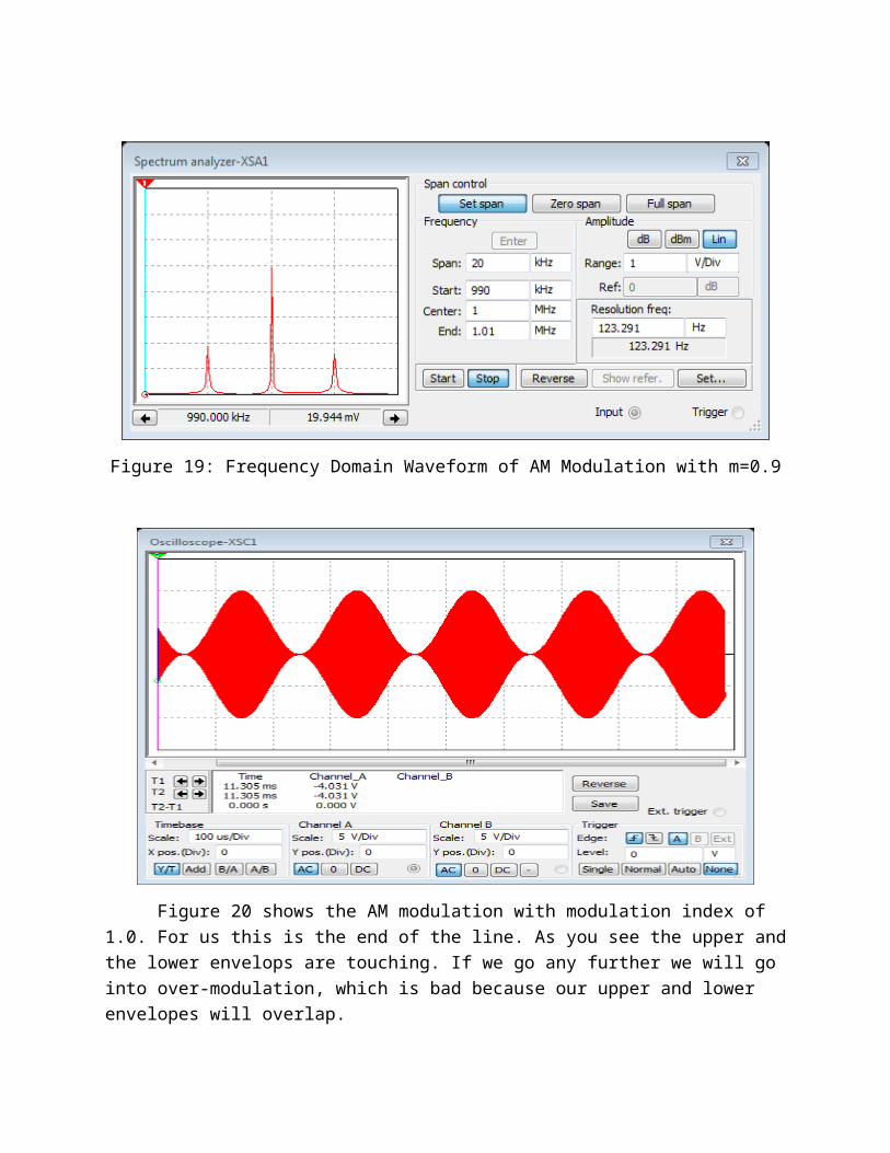
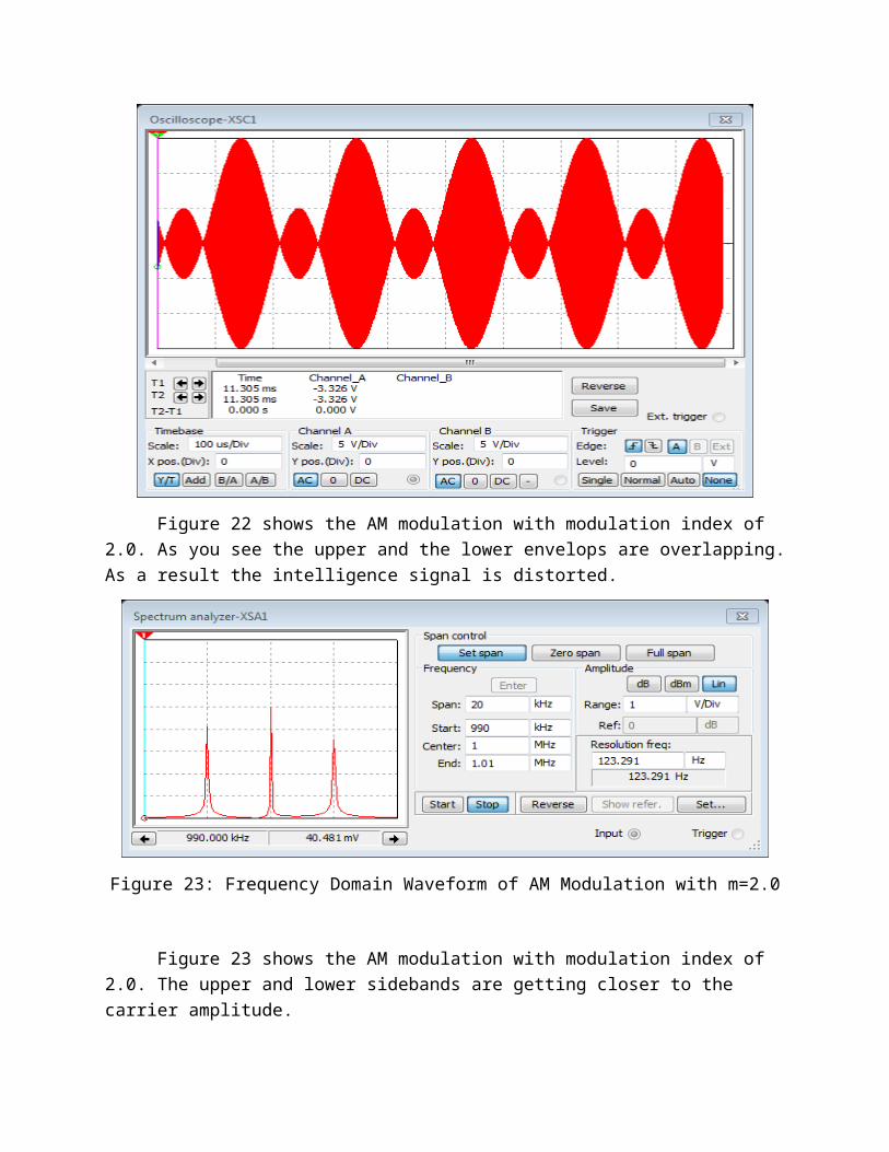
Figure 22 shows the AM modulation with modulation index of 2.0. As you see the upper and the lower envelops are overlapping. As a result the intelligence signal is distorted.
Figure 23: Frequency Domain Waveform of AM Modulation with m=2.0
Figure 23 shows the AM modulation with modulation index of 2.0. The upper and lower sidebands are getting closer to the carrier amplitude.
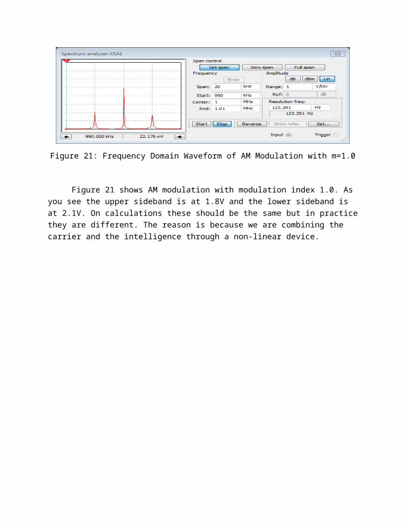
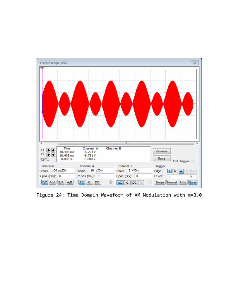
Figure 24: Time Domain Waveform of AM Modulation with m=3.0
Figure 25: Frequency Domain Waveform of AM Modulation with m=3.0
Setting A B Calculated Error Voltage @ f1 Voltage @ fs Voltage @ f2 Voltage @ f1 Voltage @ fs Voltage @ f2 @ f1 @fs @f20.1 9 11 0.1 0% 0.25 5 0.25 0.1 5 0.1 -60% 0% -60%0.2 8 12 0.2 0% 0.5 5 0.5 0.2 5 0.2 -60% 0% -60%0.3 7 13 0.3 0% 0.75 5 0.75 0.25 5 0.25 -67% 0% -67%0.4 6 14 0.4 0% 1 5 1 0.8 5 0.7 -20% 0% -30%0.5 5 15 0.5 0% 1.25 5 1.25 1 5 0.9 -20% 0% -28%0.6 4 16 0.6 0% 1.5 5 1.5 1.2 5 1 -20% 0% -33%0.7 3 17 0.7 0% 1.75 5 1.75 1.5 5 1.2 -14% 0% -31%0.8 2 18 0.8 0% 2 5 2 1.6 5 1.3 -20% 0% -35%0.9 1 19 0.9 0% 2.25 5 2.25 1.9 5 1.6 -16% 0% -29%1 0 20 1 0% 2.5 5 2.5 2.1 5 1.8 -16% 0% -28%2 30 -10 -2 -200% 5 5 5 4.1 5 3.5 -18% 0% -30%3 40 -20 -3 -200% 7.5 5 7.5 6.1 5 5.3 -19% 0% -29%
Calculated Measuredm= % Error
Table 1: Amplitude Modulation Data
The data table (Table 1) shows the Amplitude Modulation of 5 kHz intelligence signal with 1MHz carrier signal with modulation index varying from 0.1 up to 3.0.
Modulation / Demodulation
Figure 26: Schematic Diagram of AM Demodulator
The schematic shown in Figure 26 is AM modulator / demodulator. Modulation is impressing a low-frequency intelligence signal onto a higher-frequency carrier and demodulation is the process of removing the intelligence signal from the higher-frequency carrier in the receiver. The circuit is setup for modulating 1 MHz carrier signal with 5 kHz intelligence signal with modulation index of 1.0 and after that demodulating it.

Figure 27: Time Domain Waveform of AM Modulation with m=1.0
The AM waveform shown in Figure 27 is basically a signal at carrier frequency (1 MHz) whose amplitude is changing at the same rate as the intelligence frequency (5 kHz). The top and the bottom envelopes are replicas of the frequency and amplitude of the intelligence (the bottom envelope has 180° phase shift. However, the AM waveform does not include any component at the intelligence frequency.
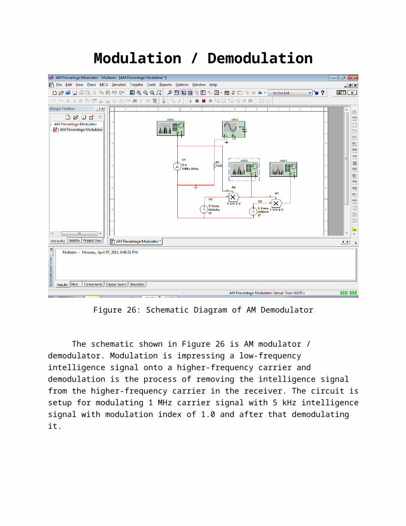
Figure 28: RF Frequency Domain Waveform of AM Modulation with m=1.0
The spectrum analyzer in Figure 28 shows upperside band of approximately 1.8V and lower sideband of approximately 2.1V. The upper and the lower sidebands are with different amplitudes because a non-linear device is used for combining the carrier and the intelligence. The carrier frequency is at 5V
Figure 29: Local Oscillator #1 Frequency Domain Waveform of AM Modulation with m=1.0
Figure 29 shows the spectrum analyzer output of the first mixer stage. The mixer is combining the AM modulated signal with 550 kHz frequency drawn from Local Oscillator #1. This is done to bring down the frequency. The result of this is 455 kHz.
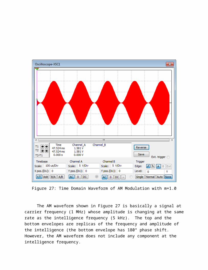
Figure 30: Local Oscillator #2 Frequency Domain Waveform of AM Modulation with m=1.0
Figure 30 shows the spectrum analyzer output of the second mixer stage, which is actually the circuit output. The second mixer is combining the 455 kHz with 450 kHz drawn from Local Oscillator #2. And the end result is 5 kHz which happens to be the intelligence signal
In short Figure 28 shows the AM modulation of 5kHz (intelligence) signal whit 1MHz (carrier) signal. For demodulating the signal, we are bringing down the frequency by using the Local Oscillator #1 set to 550Hz. So we end up with sidebands at 445Hz and 455Hz. To get to the intelligence signal, we are using Local Oscillator #2 set to 450Hz. So we end up with the intelligence signal (5kHz) and some bleed through.
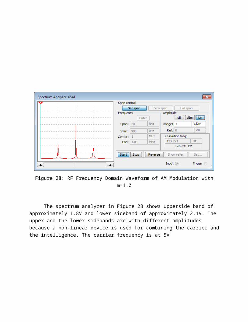
Figure 1: Schematic Diagram of AM Modulator
The schematic shown in Figure 1 is AM modulator. Modulation is impressing a low-frequency intelligence signal onto a higher-frequency carrier. We will simulate AM modulation of 1 MHz carrier signal with 5 kHz intelligence signal, as we vary the modulating index m from 0.1 to 3.0, and as explore the different responses.


![AM FM RAD-F439N AudioComm AM/FM o IPX4 c0920 ... FM RAD-F439N AudioComm AM/FM o IPX4 c0920 : 2003(lEC FFM] DC6V AM 530—1605 kHz FM 76—99 IPX4 AM : / FM : *l. JIS 4. valid only](https://img.pdfslide.net/doc/110x75/5aea079a7f8b9a6d4f918832/am-fm-rad-f439n-audiocomm-amfm-o-ipx4-c0920-fm-rad-f439n-audiocomm-amfm-o.jpg)