Embed Size (px)
Citation preview
AMBA® AXI ProtocolVersion: 2.0
Specification
Copyright © 2003-2010 ARM. All rights reserved.ARM IHI 0022C (ID030510)
AMBA AXI ProtocolSpecification
Copyright © 2003-2010 ARM. All rights reserved.
Release Information
The following changes have been made to this book.
Proprietary Notice
Words and logos marked with ® or ™ are registered trademarks or trademarks of ARM in the EU and other countries, except as otherwise stated below in this proprietary notice. Other brands and names mentioned herein may be the trademarks of their respective owners.
Neither the whole nor any part of the information contained in, or the product described in, this document may be adapted or reproduced in any material form except with the prior written permission of the copyright holder.
The product described in this document is subject to continuous developments and improvements. All particulars of the product and its use contained in this document are given by ARM in good faith. However, all warranties implied or expressed, including but not limited to implied warranties of merchantability, or fitness for purpose, are excluded.
This document is intended only to assist the reader in the use of the product. ARM shall not be liable for any loss or damage arising from the use of any information in this document, or any error or omission in such information, or any incorrect use of the product.
Where the term ARM is used it means “ARM or any of its subsidiaries as appropriate”.
ARM AMBA Specification Licence
THIS END USER LICENCE AGREEMENT (“LICENCE”) IS A LEGAL AGREEMENT BETWEEN YOU (EITHER A SINGLE INDIVIDUAL, OR SINGLE LEGAL ENTITY) AND ARM LIMITED (“ARM”) FOR THE USE OF THE RELEVANT AMBA SPECIFICATION ACCOMPANYING THIS LICENCE. ARM IS ONLY WILLING TO LICENSE THE RELEVANT AMBA SPECIFICATION TO YOU ON CONDITION THAT YOU ACCEPT ALL OF THE TERMS IN THIS LICENCE. BY CLICKING “I AGREE” OR OTHERWISE USING OR COPYING THE RELEVANT AMBA SPECIFICATION YOU INDICATE THAT YOU AGREE TO BE BOUND BY ALL THE TERMS OF THIS LICENCE. IF YOU DO NOT AGREE TO THE TERMS OF THIS LICENCE, ARM IS UNWILLING TO LICENSE THE RELEVANT AMBA SPECIFICATION TO YOU AND YOU MAY NOT USE OR COPY THE RELEVANT AMBA SPECIFICATION AND YOU SHOULD PROMPTLY RETURN THE RELEVANT AMBA SPECIFICATION TO ARM.
“LICENSEE” means You and your Subsidiaries.
“Subsidiary” means, if You are a single entity, any company the majority of whose voting shares is now or hereafter owned or controlled, directly or indirectly, by You. A company shall be a Subsidiary only for the period during which such control exists.
1. Subject to the provisions of Clauses 2, 3 and 4, ARM hereby grants to LICENSEE a perpetual, non-exclusive, non-transferable, royalty free, worldwide licence to:
(i) use and copy the relevant AMBA Specification for the purpose of developing and having developed products that comply with the relevant AMBA Specification;
(ii) manufacture and have manufactured products which either: (a) have been created by or for LICENSEE under the licence granted in Clause 1(i); or (b) incorporate a product(s) which has been created by a third party(s) under a licence granted by ARM in Clause 1(i) of such third party’s ARM AMBA Specification Licence; and
Change history
Date Issue Confidentiality Change
16 June 2003 A Non-Confidential First release
19 March 2004 B Non-Confidential First release of V1.0
03 March 2010 C Non-Confidential First release of V2.0
ARM IHI 0022C Copyright © 2003-2010 ARM. All rights reserved. iiID030510 Non-Confidential
(iii) offer to sell, sell, supply or otherwise distribute products which have either been (a) created by or for LICENSEE under the licence granted in Clause 1(i); or (b) manufactured by or for LICENSEE under the licence granted in Clause 1(ii).
2. LICENSEE hereby agrees that the licence granted in Clause 1 is subject to the following restrictions:
(i) where a product created under Clause 1(i) is an integrated circuit which includes a CPU then either: (a) such CPU shall only be manufactured under licence from ARM; or (b) such CPU is neither substantially compliant with nor marketed as being compliant with the ARM instruction sets licensed by ARM from time to time;
(ii) the licences granted in Clause 1(iii) shall not extend to any portion or function of a product that is not itself compliant with part of the relevant AMBA Specification; and
(iii) no right is granted to LICENSEE to sublicense the rights granted to LICENSEE under this Agreement.
3. Except as specifically licensed in accordance with Clause 1, LICENSEE acquires no right, title or interest in any ARM technology or any intellectual property embodied therein. In no event shall the licences granted in accordance with Clause 1 be construed as granting LICENSEE, expressly or by implication, estoppel or otherwise, a licence to use any ARM technology except the relevant AMBA Specification.
4. THE RELEVANT AMBA SPECIFICATION IS PROVIDED “AS IS” WITH NO WARRANTIES EXPRESS, IMPLIED OR STATUTORY, INCLUDING BUT NOT LIMITED TO ANY WARRANTY OF SATISFACTORY QUALITY, MERCHANTABILITY, NONINFRINGEMENT OR FITNESS FOR A PARTICULAR PURPOSE.
5. No licence, express, implied or otherwise, is granted to LICENSEE, under the provisions of Clause 1, to use the ARM tradename, or AMBA trademark in connection with the relevant AMBA Specification or any products based thereon. Nothing in Clause 1 shall be construed as authority for LICENSEE to make any representations on behalf of ARM in respect of the relevant AMBA Specification.
6. This Licence shall remain in force until terminated by you or by ARM. Without prejudice to any of its other rights if LICENSEE is in breach of any of the terms and conditions of this Licence then ARM may terminate this Licence immediately upon giving written notice to You. You may terminate this Licence at any time. Upon expiry or termination of this Licence by You or by ARM LICENSEE shall stop using the relevant AMBA Specification and destroy all copies of the relevant AMBA Specification in your possession together with all documentation and related materials. Upon expiry or termination of this Licence, the provisions of clauses 6 and 7 shall survive.
7. The validity, construction and performance of this Agreement shall be governed by English Law.
ARM contract references: LEC-PRE-00490-V4.0 ARM AMBA Specification Licence
Confidentiality Status
This document is Non-Confidential. The right to use, copy and disclose this document may be subject to license restrictions in accordance with the terms of the agreement entered into by ARM and the party that ARM delivered this document to.
Unrestricted Access is an ARM internal classification.
Product Status
The information in this document is final, that is for a developed product.
Web Address
http://www.arm.com
ARM IHI 0022C Copyright © 2003-2010 ARM. All rights reserved. iiiID030510 Non-Confidential
ContentsAMBA AXI Protocol Specification
PrefaceAbout this book ............................................................................................................ xFeedback .................................................................................................................. xiii
Chapter 1 Introduction1.1 About the AXI protocol ............................................................................................. 1-21.2 Architecture .............................................................................................................. 1-41.3 Basic transactions .................................................................................................... 1-71.4 Additional features ................................................................................................. 1-10
Chapter 2 Signal Descriptions2.1 Global signals .......................................................................................................... 2-22.2 Write address channel signals ................................................................................. 2-32.3 Write data channel signals ....................................................................................... 2-42.4 Write response channel signals ............................................................................... 2-52.5 Read address channel signals ................................................................................. 2-62.6 Read data channel signals ...................................................................................... 2-72.7 Low-power interface signals .................................................................................... 2-8
Chapter 3 Channel Handshake3.1 Handshake process ................................................................................................. 3-23.2 Relationships between the channels ....................................................................... 3-53.3 Dependencies between channel handshake signals ............................................... 3-6
Chapter 4 Addressing Options4.1 About addressing options ........................................................................................ 4-24.2 Burst length .............................................................................................................. 4-34.3 Burst size ................................................................................................................. 4-4
ARM IHI 0022C Copyright © 2003-2010 ARM. All rights reserved. ivID030510 Non-Confidential
Contents
4.4 Burst type ................................................................................................................. 4-54.5 Burst address ........................................................................................................... 4-7
Chapter 5 Additional Control Information5.1 Cache support ......................................................................................................... 5-25.2 Protection unit support ............................................................................................. 5-4
Chapter 6 Atomic Accesses6.1 About atomic accesses ............................................................................................ 6-26.2 Exclusive access ..................................................................................................... 6-36.3 Locked access ......................................................................................................... 6-6
Chapter 7 Response Signaling7.1 About response signaling ........................................................................................ 7-27.2 Response types ....................................................................................................... 7-3
Chapter 8 Ordering Model8.1 About the Ordering model ........................................................................................ 8-28.2 Transfer ID fields ..................................................................................................... 8-38.3 Read ordering .......................................................................................................... 8-48.4 Normal write ordering .............................................................................................. 8-58.5 Write data interleaving ............................................................................................. 8-68.6 Read and write interaction ....................................................................................... 8-78.7 Interconnect use of ID fields .................................................................................... 8-88.8 Recommended width of ID fields ............................................................................. 8-9
Chapter 9 Data Buses9.1 About the data buses ............................................................................................... 9-29.2 Write strobes ............................................................................................................ 9-39.3 Narrow transfers ...................................................................................................... 9-49.4 Byte invariance ........................................................................................................ 9-5
Chapter 10 Unaligned Transfers10.1 About unaligned transfers ...................................................................................... 10-210.2 Examples ............................................................................................................... 10-3
Chapter 11 Clock and Reset11.1 Clock and reset requirements ................................................................................ 11-2
Chapter 12 Low-power Interface12.1 About the low-power interface ............................................................................... 12-212.2 Low-power clock control ........................................................................................ 12-3
Chapter 13 AXI413.1 Burst support ......................................................................................................... 13-213.2 Quality of service signaling .................................................................................... 13-313.3 Multiple region interfaces ....................................................................................... 13-513.4 Write response dependencies ............................................................................... 13-613.5 AWCACHE and ARCACHE Attributes ................................................................... 13-813.6 Ordering requirements for Non-modifiable transactions ...................................... 13-1013.7 Updated meaning of Read Allocate and Write Allocate ....................................... 13-1113.8 Memory types ...................................................................................................... 13-1413.9 Mismatched Attributes ......................................................................................... 13-1913.10 Transaction buffering ........................................................................................... 13-2013.11 Use of device memory types ............................................................................... 13-2113.12 Legacy considerations ......................................................................................... 13-2213.13 Ordering model .................................................................................................... 13-2313.14 User signals ......................................................................................................... 13-28
ARM IHI 0022C Copyright © 2003-2010 ARM. All rights reserved. vID030510 Non-Confidential
Contents
13.15 Locked transactions ............................................................................................. 13-2913.16 Write interleaving ................................................................................................. 13-3013.17 Interoperability and default signals ...................................................................... 13-31
Chapter 14 AXI4-Lite14.1 Introduction ............................................................................................................ 14-214.2 Definition of AXI4-Lite ............................................................................................ 14-314.3 Interoperability ....................................................................................................... 14-614.4 Defined conversion mechanism ............................................................................. 14-714.5 Conversion, Protection, and Detection .................................................................. 14-9
Appendix A Revisions
ARM IHI 0022C Copyright © 2003-2010 ARM. All rights reserved. viID030510 Non-Confidential
ARM IHI 0022C Copyright © 2003-2010 ARM. All rights reserved. viiID030510 Non-Confidential
List of TablesAMBA AXI Protocol Specification
Change history ................................................................................................................................ iiTable 2-1 Global signals ............................................................................................................................. 2-2Table 2-2 Write address channel signals .................................................................................................... 2-3Table 2-3 Write data channel signals .......................................................................................................... 2-4Table 2-4 Write response channel signals .................................................................................................. 2-5Table 2-5 Read address channel signals .................................................................................................... 2-6Table 2-6 Read data channel signals .......................................................................................................... 2-7Table 2-7 Low-power interface signals ....................................................................................................... 2-8Table 4-1 Burst length encoding ................................................................................................................. 4-3Table 4-2 Burst size encoding ..................................................................................................................... 4-4Table 4-3 Burst type encoding .................................................................................................................... 4-5Table 5-1 Cache encoding .......................................................................................................................... 5-3Table 5-2 Protection encoding .................................................................................................................... 5-4Table 6-1 Atomic access encoding ............................................................................................................. 6-2Table 7-1 RRESP[1:0] and BRESP[1:0] encoding ...................................................................................... 7-2Table 13-1 Parameters fixed as Non-modifiable ......................................................................................... 13-8Table 13-2 AWCACHE bit allocations ....................................................................................................... 13-12Table 13-3 ARCACHE bit allocations ........................................................................................................ 13-13Table 13-4 Memory type encoding ............................................................................................................ 13-14Table 13-5 Summary of ordering requirements ........................................................................................ 13-25Table 13-6 Atomic access encoding ......................................................................................................... 13-29Table 13-7 Write channel signals and default signal values ..................................................................... 13-33Table 13-8 Read channel signals and default signals values ................................................................... 13-34Table 14-1 AXI4-Lite interface signals ........................................................................................................ 14-3Table 14-2 Full AXI and AXI4-Lite interoperability ...................................................................................... 14-6Table A-1 Issue B ........................................................................................................................................ A-1Table A-2 Differences between issue B and issue C .................................................................................. A-1
ARM IHI 0022C Copyright © 2003-2010 ARM. All rights reserved. viiiID030510 Non-Confidential
List of FiguresAMBA AXI Protocol Specification
Key to timing diagram conventions ............................................................................................... xiiFigure 1-1 Channel architecture of reads ..................................................................................................... 1-4Figure 1-2 Channel architecture of writes .................................................................................................... 1-4Figure 1-3 Interface and interconnect .......................................................................................................... 1-6Figure 1-4 Read burst .................................................................................................................................. 1-7Figure 1-5 Overlapping read bursts .............................................................................................................. 1-8Figure 1-6 Write burst ................................................................................................................................... 1-8Figure 3-1 VALID before READY handshake .............................................................................................. 3-2Figure 3-2 READY before VALID handshake .............................................................................................. 3-2Figure 3-3 VALID with READY handshake .................................................................................................. 3-3Figure 3-4 Read transaction handshake dependencies ............................................................................... 3-6Figure 3-5 Write transaction handshake dependencies ............................................................................... 3-6Figure 9-1 Byte lane mapping ...................................................................................................................... 9-3Figure 9-2 Narrow transfer example with 8-bit transfers .............................................................................. 9-4Figure 9-3 Narrow transfer example with 32-bit transfers ............................................................................ 9-4Figure 9-4 Example mixed-endian data structure ........................................................................................ 9-5Figure 10-1 Aligned and unaligned word transfers on a 32-bit bus .............................................................. 10-3Figure 10-2 Aligned and unaligned word transfers on a 64-bit bus .............................................................. 10-4Figure 10-3 Aligned wrapping word transfers on a 64-bit bus ...................................................................... 10-4Figure 11-1 Exit from reset ........................................................................................................................... 11-2Figure 12-1 CSYSREQ and CSYSACK handshake ..................................................................................... 12-3Figure 12-2 Acceptance of a low-power request .......................................................................................... 12-4Figure 12-3 Denial of a low-power request .................................................................................................. 12-4Figure 12-4 Low-power clock control sequence ........................................................................................... 12-5Figure 13-1 Slave write response dependencies ......................................................................................... 13-6Figure 13-2 Example system with different single-copy atomic groups ..................................................... 13-27

Preface
This preface introduces the AMBA 4 Advanced eXtensible Interface (AXI4) Protocol Specification. It contains the following sections:• About this book on page x• Feedback on page xiii.
ARM IHI 0022C Copyright © 2003-2010 ARM. All rights reserved. ixID030510 Non-Confidential
Preface
About this bookThis book is for AMBA AXI Protocol Specification.
Intended audience
This book is written for hardware and software engineers who want to become familiar with the Advanced Microcontroller Bus Architecture (AMBA) and design systems and modules that are compatible with the AMBA AXI protocol.
Using this book
This book is organized into the following chapters:
Chapter 1 Introduction Read this for a description of the architecture of the AXI protocol and the basic transactions that the protocol defines.
Chapter 2 Signal Descriptions Read this for definitions of the AXI global, write address channel, write data channel, write response channel, read address channel, read data channel, and low-power interface signals.
Chapter 3 Channel Handshake Read this for the AXI channel handshake process.
Chapter 4 Addressing Options Read this for AXI burst types and how to calculate addresses and byte lanes for transfers within a burst.
Chapter 5 Additional Control Information Read this for how to use the AXI protocol to support system level caches and protection units.
Chapter 6 Atomic Accesses Read this for how to perform exclusive accesses and locked accesses.
Chapter 7 Response Signaling Read this for the four transaction responses of AXI slaves.
Chapter 8 Ordering Model Read this for how the AXI protocol uses transaction ID tags to enable out-of-order transaction processing.
Chapter 9 Data Buses Read this for how to do transactions of varying sizes on the AXI read and write data buses and how to use byte-invariant endianness to handle mixed-endian data.
Chapter 10 Unaligned Transfers Read this for how the AXI protocol handles unaligned transfers.
Chapter 11 Clock and Reset Read this for the timing of the AXI clock and reset signals.
ARM IHI 0022C Copyright © 2003-2010 ARM. All rights reserved. xID030510 Non-Confidential
Preface
Chapter 12 Low-power Interface Read this for how to use the AXI clock control interface to enter into and exit from a low-power state.
Chapter 13 AXI4 Read this for a description of the technical changes between AXI3 and AXI4 versions of the AXI protocol.
Chapter 14 AXI4-Lite Read this for a description of the AXI4-Lite interface, a simpler control register style interface for use when the full functionality of AXI4 is not required.
Appendix A Revisions Read this for a description of the technical changes between released issues of this book.
Conventions
Conventions that this book can use are described in:• Typographical• Timing diagrams on page xii• Signals on page xii.
Typographical
The typographical conventions are:
italic Highlights important notes, introduces special terminology, denotes internal cross-references, and citations.
bold Highlights interface elements, such as menu names. Denotes signal names. Also used for terms in descriptive lists, where appropriate.
monospace Denotes text that you can enter at the keyboard, such as commands, file and program names, and source code.
monospace Denotes a permitted abbreviation for a command or option. You can enter the underlined text instead of the full command or option name.
monospace italic Denotes arguments to monospace text where the argument is to be replaced by a specific value.
monospace bold Denotes language keywords when used outside example code.
< and > Enclose replaceable terms for assembler syntax where they appear in code or code fragments. For example:MRC p15, 0 <Rd>, <CRn>, <CRm>, <Opcode_2>
ARM IHI 0022C Copyright © 2003-2010 ARM. All rights reserved. xiID030510 Non-Confidential
Preface
Timing diagrams
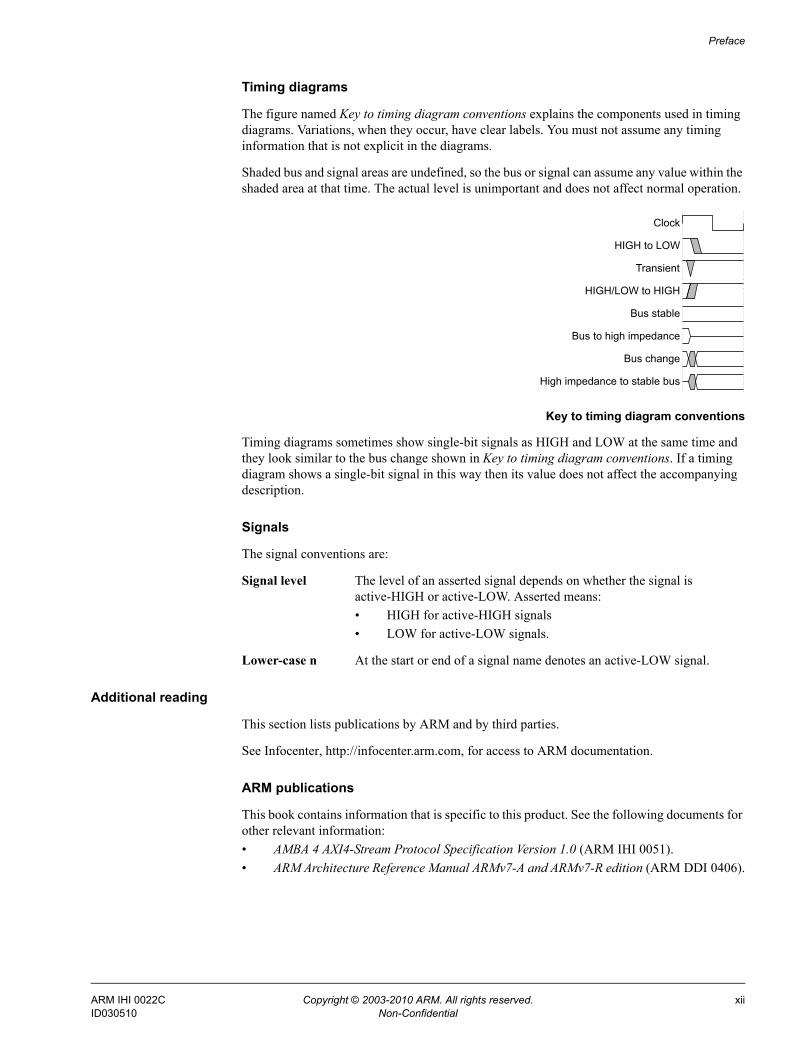
The figure named Key to timing diagram conventions explains the components used in timing diagrams. Variations, when they occur, have clear labels. You must not assume any timing information that is not explicit in the diagrams.
Shaded bus and signal areas are undefined, so the bus or signal can assume any value within the shaded area at that time. The actual level is unimportant and does not affect normal operation.
Key to timing diagram conventions
Timing diagrams sometimes show single-bit signals as HIGH and LOW at the same time and they look similar to the bus change shown in Key to timing diagram conventions. If a timing diagram shows a single-bit signal in this way then its value does not affect the accompanying description.
Signals
The signal conventions are:
Signal level The level of an asserted signal depends on whether the signal is active-HIGH or active-LOW. Asserted means:• HIGH for active-HIGH signals• LOW for active-LOW signals.
Lower-case n At the start or end of a signal name denotes an active-LOW signal.
Additional reading
This section lists publications by ARM and by third parties.
See Infocenter, http://infocenter.arm.com, for access to ARM documentation.
ARM publications
This book contains information that is specific to this product. See the following documents for other relevant information:• AMBA 4 AXI4-Stream Protocol Specification Version 1.0 (ARM IHI 0051).• ARM Architecture Reference Manual ARMv7-A and ARMv7-R edition (ARM DDI 0406).
Clock
HIGH to LOW
Transient
HIGH/LOW to HIGH
Bus stable
Bus to high impedance
Bus change
High impedance to stable bus
ARM IHI 0022C Copyright © 2003-2010 ARM. All rights reserved. xiiID030510 Non-Confidential
Preface
FeedbackARM welcomes feedback on this protocol and its documentation.
Feedback on this protocol
If you have any comments or suggestions about this protocol, contact your supplier and give:
• The name.
• The revision or version.
• An explanation with as much information as you can provide. Include symptoms and diagnostic procedures if appropriate.
Feedback on content
If you have comments on content then send an e-mail to [email protected]. Give:• the title, AMBA AXI Protocol Specification• the number, ARM IHI 0022C• the page numbers to which your comments apply• a concise explanation of your comments.
ARM also welcomes general suggestions for additions and improvements.
ARM IHI 0022C Copyright © 2003-2010 ARM. All rights reserved. xiiiID030510 Non-Confidential
Chapter 1 Introduction
This chapter describes the architecture of the AXI protocol and the basic transactions that the protocol defines. It contains the following sections:• About the AXI protocol on page 1-2• Architecture on page 1-4• Basic transactions on page 1-7• Additional features on page 1-10.
ARM IHI 0022C Copyright © 2003-2010 ARM. All rights reserved. 1-1ID030510 Non-Confidential
Introduction
1.1 About the AXI protocolThe AMBA AXI protocol is targeted at high-performance, high-frequency system designs and includes a number of features that make it suitable for a high-speed submicron interconnect.
The objectives of the latest generation AMBA interface are to:• be suitable for high-bandwidth and low-latency designs• enable high-frequency operation without using complex bridges• meet the interface requirements of a wide range of components• be suitable for memory controllers with high initial access latency• provide flexibility in the implementation of interconnect architectures• be backward-compatible with existing AHB and APB interfaces.
The key features of the AXI protocol are:• separate address/control and data phases• support for unaligned data transfers using byte strobes• burst-based transactions with only start address issued• separate read and write data channels to enable low-cost Direct Memory Access (DMA)• ability to issue multiple outstanding addresses• out-of-order transaction completion• easy addition of register stages to provide timing closure.
As well as the data transfer protocol, the AXI protocol includes optional extensions that cover signaling for low-power operation.
1.1.1 AXI revisions
The AXI protocol has been an industry standard for many years and the AMBA AXI Protocol Specification Version 1.0 describes the AXI Interface.
This revision, Version 2.0 of the document, includes all the information on the original AXI protocol specification, now referred to as AXI3, and two new chapters, detailing AXI4 and AXI4-Lite.
AXI4
The AXI4 update to AXI3 includes the following:• support for burst lengths up to 256 beats• Quality of Service (QoS) signaling• support for multiple region interfaces• updated write response requirements• updated AWCACHE and ARCACHE signaling details• additional information on Ordering requirements• details of optional User signaling• removal of locked transactions• removal of write interleaving
.
AXI4 also includes information on the use of default signaling and discusses the interoperability of components.
ARM IHI 0022C Copyright © 2003-2010 ARM. All rights reserved. 1-2ID030510 Non-Confidential
Introduction
AXI4-Lite
AXI4-Lite is a subset of the AXI4 protocol that is intended for communication with control register-style interfaces in components and allows simpler component interfaces to be built.
The key features of the AXI4-Lite interface are:• all transactions are burst length of 1• all data accesses are the same size as the width of the data bus• support for data bus width of 32-bit or 64-bit• all accesses are equivalent to AWCACHE or ARCACHE equal to b0000• exclusive accesses are not supported.
ARM IHI 0022C Copyright © 2003-2010 ARM. All rights reserved. 1-3ID030510 Non-Confidential
Introduction
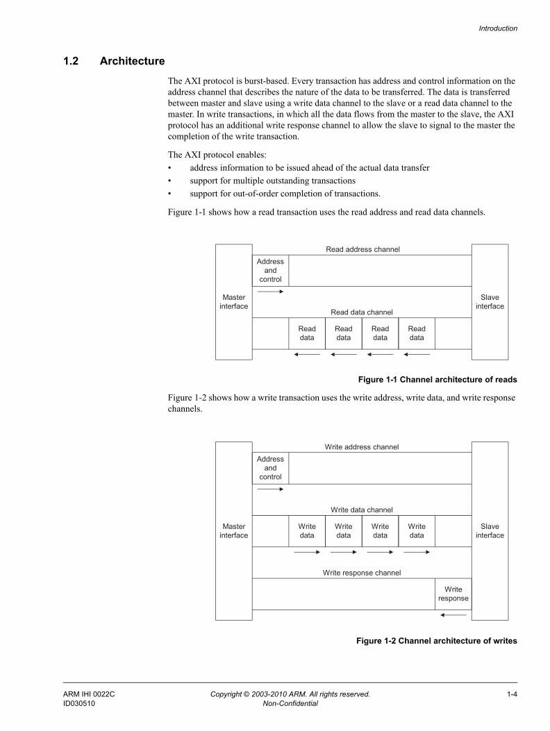
1.2 ArchitectureThe AXI protocol is burst-based. Every transaction has address and control information on the address channel that describes the nature of the data to be transferred. The data is transferred between master and slave using a write data channel to the slave or a read data channel to the master. In write transactions, in which all the data flows from the master to the slave, the AXI protocol has an additional write response channel to allow the slave to signal to the master the completion of the write transaction.
The AXI protocol enables:• address information to be issued ahead of the actual data transfer• support for multiple outstanding transactions • support for out-of-order completion of transactions.
Figure 1-1 shows how a read transaction uses the read address and read data channels.
Figure 1-1 Channel architecture of reads
Figure 1-2 shows how a write transaction uses the write address, write data, and write response channels.
Figure 1-2 Channel architecture of writes
Master
interface
Slave
interface
Address
and
control
Read address channel
Read
data
Read
data
Read
data
Read
data
Read data channel
Master
interface
Slave
interface
Address
and
control
Write address channel
Write
data
Write data channel
Write
data
Write
data
Write
data
Write
response
Write response channel
ARM IHI 0022C Copyright © 2003-2010 ARM. All rights reserved. 1-4ID030510 Non-Confidential
Introduction
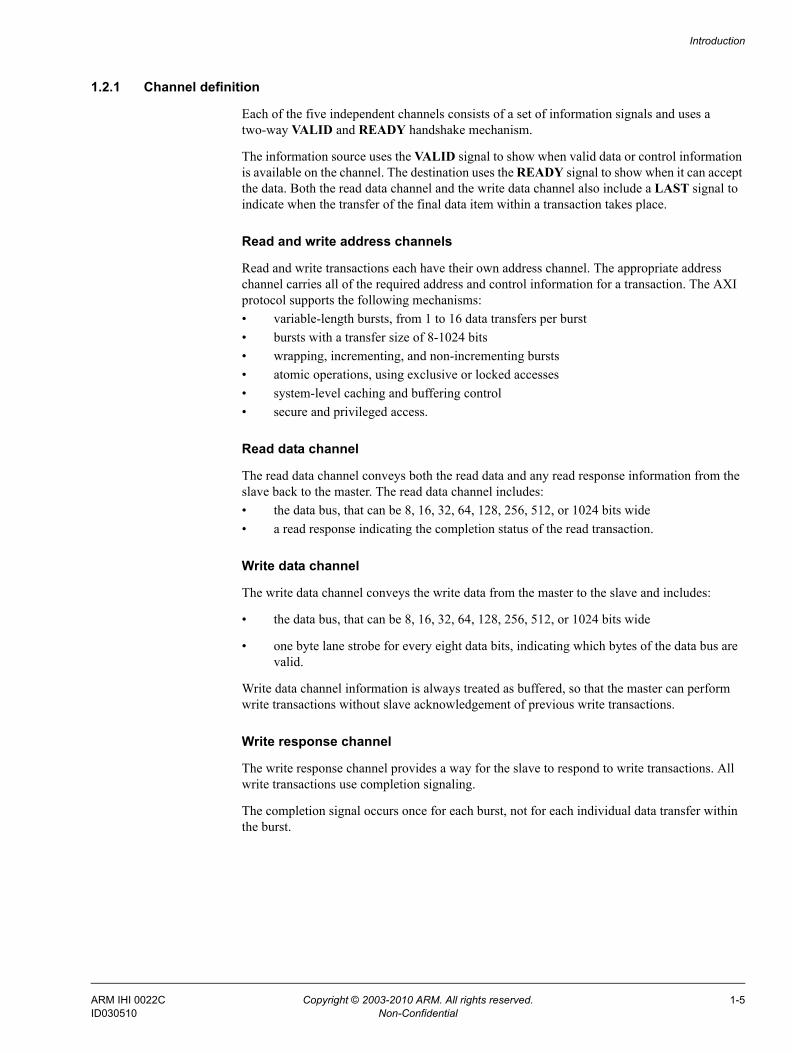
1.2.1 Channel definition
Each of the five independent channels consists of a set of information signals and uses a two-way VALID and READY handshake mechanism.
The information source uses the VALID signal to show when valid data or control information is available on the channel. The destination uses the READY signal to show when it can accept the data. Both the read data channel and the write data channel also include a LAST signal to indicate when the transfer of the final data item within a transaction takes place.
Read and write address channels
Read and write transactions each have their own address channel. The appropriate address channel carries all of the required address and control information for a transaction. The AXI protocol supports the following mechanisms: • variable-length bursts, from 1 to 16 data transfers per burst• bursts with a transfer size of 8-1024 bits• wrapping, incrementing, and non-incrementing bursts• atomic operations, using exclusive or locked accesses • system-level caching and buffering control• secure and privileged access.
Read data channel
The read data channel conveys both the read data and any read response information from the slave back to the master. The read data channel includes:• the data bus, that can be 8, 16, 32, 64, 128, 256, 512, or 1024 bits wide• a read response indicating the completion status of the read transaction.
Write data channel
The write data channel conveys the write data from the master to the slave and includes:
• the data bus, that can be 8, 16, 32, 64, 128, 256, 512, or 1024 bits wide
• one byte lane strobe for every eight data bits, indicating which bytes of the data bus are valid.
Write data channel information is always treated as buffered, so that the master can perform write transactions without slave acknowledgement of previous write transactions.
Write response channel
The write response channel provides a way for the slave to respond to write transactions. All write transactions use completion signaling.
The completion signal occurs once for each burst, not for each individual data transfer within the burst.
ARM IHI 0022C Copyright © 2003-2010 ARM. All rights reserved. 1-5ID030510 Non-Confidential
Introduction
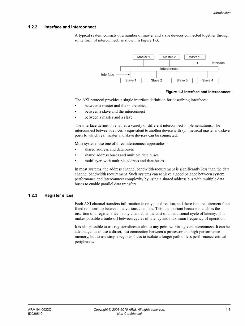
1.2.2 Interface and interconnect
A typical system consists of a number of master and slave devices connected together through some form of interconnect, as shown in Figure 1-3.
Figure 1-3 Interface and interconnect
The AXI protocol provides a single interface definition for describing interfaces:• between a master and the interconnect• between a slave and the interconnect• between a master and a slave.
The interface definition enables a variety of different interconnect implementations. The interconnect between devices is equivalent to another device with symmetrical master and slave ports to which real master and slave devices can be connected.
Most systems use one of three interconnect approaches:• shared address and data buses• shared address buses and multiple data buses• multilayer, with multiple address and data buses.
In most systems, the address channel bandwidth requirement is significantly less than the data channel bandwidth requirement. Such systems can achieve a good balance between system performance and interconnect complexity by using a shared address bus with multiple data buses to enable parallel data transfers.
1.2.3 Register slices
Each AXI channel transfers information in only one direction, and there is no requirement for a fixed relationship between the various channels. This is important because it enables the insertion of a register slice in any channel, at the cost of an additional cycle of latency. This makes possible a trade-off between cycles of latency and maximum frequency of operation.
It is also possible to use register slices at almost any point within a given interconnect. It can be advantageous to use a direct, fast connection between a processor and high-performance memory, but to use simple register slices to isolate a longer path to less performance-critical peripherals.
Interconnect
Slave 1 Slave 2 Slave 3 Slave 4
Master 1 Master 2 Master 3
Interface
Interface
ARM IHI 0022C Copyright © 2003-2010 ARM. All rights reserved. 1-6ID030510 Non-Confidential
Introduction
1.3 Basic transactionsThis section gives examples of basic AXI protocol transactions. Each example shows the VALID and READY handshake mechanism. Transfer of either address information or data occurs when both the VALID and READY signals are HIGH. The examples are provided in:• Read burst example• Overlapping read burst example on page 1-8• Write burst example on page 1-8.
This section also describes Transaction ordering on page 1-9.
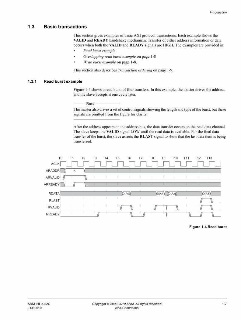
1.3.1 Read burst example
Figure 1-4 shows a read burst of four transfers. In this example, the master drives the address, and the slave accepts it one cycle later.
Note The master also drives a set of control signals showing the length and type of the burst, but these signals are omitted from the figure for clarity.
After the address appears on the address bus, the data transfer occurs on the read data channel. The slave keeps the VALID signal LOW until the read data is available. For the final data transfer of the burst, the slave asserts the RLAST signal to show that the last data item is being transferred.
Figure 1-4 Read burst
ARADDR A
T12T0 T1 T2 T3 T4 T5 T6 T7 T8 T9 T10 T11 T13
ARVALID
ARREADY
D(A0) D(A1) D(A2) D(A3)
RVALID
RDATA
RLAST
RREADY
ACLK
ARM IHI 0022C Copyright © 2003-2010 ARM. All rights reserved. 1-7ID030510 Non-Confidential
Introduction
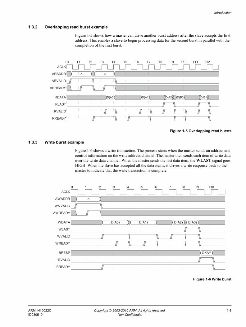
1.3.2 Overlapping read burst example
Figure 1-5 shows how a master can drive another burst address after the slave accepts the first address. This enables a slave to begin processing data for the second burst in parallel with the completion of the first burst.
Figure 1-5 Overlapping read bursts
1.3.3 Write burst example
Figure 1-6 shows a write transaction. The process starts when the master sends an address and control information on the write address channel. The master then sends each item of write data over the write data channel. When the master sends the last data item, the WLAST signal goes HIGH. When the slave has accepted all the data items, it drives a write response back to the master to indicate that the write transaction is complete.
Figure 1-6 Write burst
ARADDR A
T12T0 T1 T2 T3 T4 T5 T6 T7 T8 T9 T10 T11
ARVALID
ARREADY
B
D(A0) D(A1) D(A2) D(B0) D(B1)
RVALID
RDATA
RLAST
RREADY
ACLK
AWADDR A
T0 T1 T2 T3 T4 T5 T6 T7 T8 T9 T10
AWVALID
AWREADY
D(A0)
WVALID
WDATA
WLAST
WREADY
BVALID
BRESP
BREADY
ACLK
D(A1) D(A2) D(A3)
OKAY
ARM IHI 0022C Copyright © 2003-2010 ARM. All rights reserved. 1-8ID030510 Non-Confidential
Introduction
1.3.4 Transaction ordering
The AXI protocol enables out-of-order transaction completion. It gives an ID tag to every transaction across the interface. The protocol requires that transactions with the same ID tag are completed in order, but transactions with different ID tags can be completed out of order.
Out-of-order transactions can improve system performance in two ways:
• The interconnect can enable transactions with fast-responding slaves to complete in advance of earlier transactions with slower slaves.
• Complex slaves can return read data out of order. For example, a data item for a later access might be available from an internal buffer before the data for an earlier access is available.
If a master requires that transactions are completed in the same order that they are issued, then they must all have the same ID tag. If, however, a master does not require in-order transaction completion, it can supply the transactions with different ID tags, enabling them to be completed in any order.
In a multimaster system, the interconnect is responsible for appending additional information to the ID tag to ensure that ID tags from all masters are unique. The ID tag is similar to a master number, but with the extension that each master can implement multiple virtual masters within the same port by supplying an ID tag to indicate the virtual master number.
Although complex devices can make use of the out-of-order facility, simple devices are not required to use it. Simple masters can issue every transaction with the same ID tag, and simple slaves can respond to every transaction in order, irrespective of the ID tag.
ARM IHI 0022C Copyright © 2003-2010 ARM. All rights reserved. 1-9ID030510 Non-Confidential
Introduction
1.4 Additional featuresThe AXI protocol also supports the following additional features:
Burst types The AXI protocol supports three different burst types that are suitable for:• normal memory accesses• wrapping cache line bursts• streaming data to peripheral FIFO locations.See Chapter 4 Addressing Options.
System cache support The cache-support signal of the AXI protocol enables a master to provide to a system-level cache the bufferable, cacheable, and allocate attributes of a transaction.See Cache support on page 5-2.
Protection unit support To enable both privileged and secure accesses, the AXI protocol provides three levels of protection unit support.See Protection unit support on page 5-4.
Atomic operations The AXI protocol defines mechanisms for both exclusive and locked accesses.See Chapter 6 Atomic Accesses.
Error support The AXI protocol provides error support for both address decode errors and slave-generated errors.See Chapter 7 Response Signaling.
Unaligned address To enhance the performance of the initial accesses within a burst, the AXI protocol supports unaligned burst start addresses.See Chapter 10 Unaligned Transfers.
ARM IHI 0022C Copyright © 2003-2010 ARM. All rights reserved. 1-10ID030510 Non-Confidential
Chapter 2 Signal Descriptions
This chapter defines the AXI signals. Although bus width and transaction ID width are implementation-specific, the tables in this chapter show a 32-bit data bus, a four-bit write data strobe, and four-bit ID fields. This chapter contains the following sections:• Global signals on page 2-2• Write address channel signals on page 2-3• Write data channel signals on page 2-4• Write response channel signals on page 2-5• Read address channel signals on page 2-6• Read data channel signals on page 2-7• Low-power interface signals on page 2-8.
ARM IHI 0022C Copyright © 2003-2010 ARM. All rights reserved. 2-1ID030510 Non-Confidential

Signal Descriptions
2.1 Global signalsTable 2-1 lists the global AXI signals.
Table 2-1 Global signals
Signal Source Description
ACLK Clock source Global clock signal. All signals are sampled on the rising edge of the global clock.
ARESETn Reset source Global reset signal. This signal is active LOW.
ARM IHI 0022C Copyright © 2003-2010 ARM. All rights reserved. 2-2ID030510 Non-Confidential
Signal Descriptions
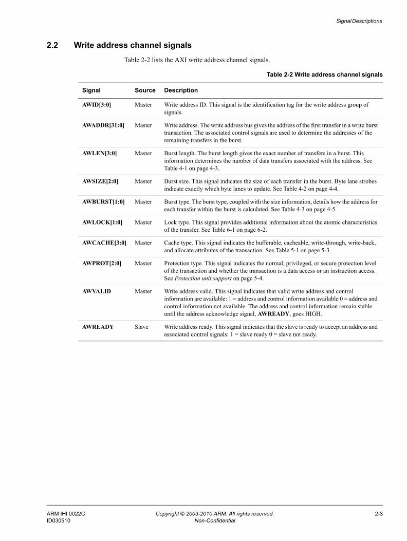
2.2 Write address channel signalsTable 2-2 lists the AXI write address channel signals.
Table 2-2 Write address channel signals
Signal Source Description
AWID[3:0] Master Write address ID. This signal is the identification tag for the write address group of signals.
AWADDR[31:0] Master Write address. The write address bus gives the address of the first transfer in a write burst transaction. The associated control signals are used to determine the addresses of the remaining transfers in the burst.
AWLEN[3:0] Master Burst length. The burst length gives the exact number of transfers in a burst. This information determines the number of data transfers associated with the address. See Table 4-1 on page 4-3.
AWSIZE[2:0] Master Burst size. This signal indicates the size of each transfer in the burst. Byte lane strobes indicate exactly which byte lanes to update. See Table 4-2 on page 4-4.
AWBURST[1:0] Master Burst type. The burst type, coupled with the size information, details how the address for each transfer within the burst is calculated. See Table 4-3 on page 4-5.
AWLOCK[1:0] Master Lock type. This signal provides additional information about the atomic characteristics of the transfer. See Table 6-1 on page 6-2.
AWCACHE[3:0] Master Cache type. This signal indicates the bufferable, cacheable, write-through, write-back, and allocate attributes of the transaction. See Table 5-1 on page 5-3.
AWPROT[2:0] Master Protection type. This signal indicates the normal, privileged, or secure protection level of the transaction and whether the transaction is a data access or an instruction access. See Protection unit support on page 5-4.
AWVALID Master Write address valid. This signal indicates that valid write address and control information are available: 1 = address and control information available 0 = address and control information not available. The address and control information remain stable until the address acknowledge signal, AWREADY, goes HIGH.
AWREADY Slave Write address ready. This signal indicates that the slave is ready to accept an address and associated control signals: 1 = slave ready 0 = slave not ready.
ARM IHI 0022C Copyright © 2003-2010 ARM. All rights reserved. 2-3ID030510 Non-Confidential
Signal Descriptions
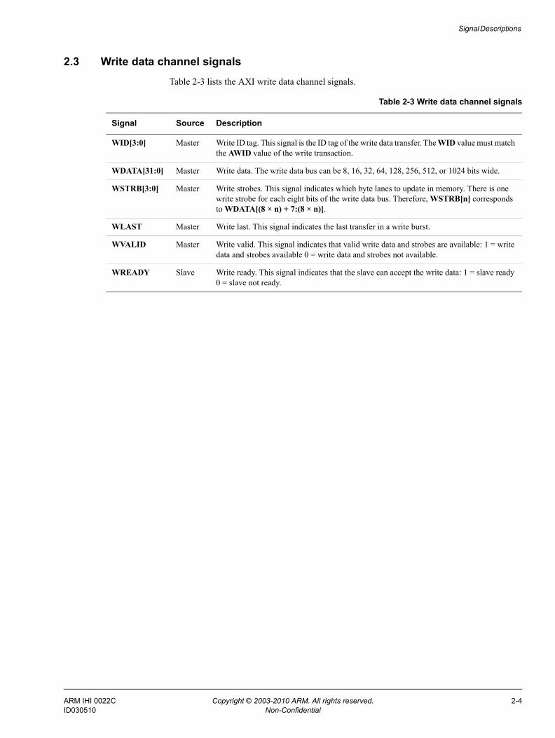
2.3 Write data channel signalsTable 2-3 lists the AXI write data channel signals.
Table 2-3 Write data channel signals
Signal Source Description
WID[3:0] Master Write ID tag. This signal is the ID tag of the write data transfer. The WID value must match the AWID value of the write transaction.
WDATA[31:0] Master Write data. The write data bus can be 8, 16, 32, 64, 128, 256, 512, or 1024 bits wide.
WSTRB[3:0] Master Write strobes. This signal indicates which byte lanes to update in memory. There is one write strobe for each eight bits of the write data bus. Therefore, WSTRB[n] corresponds to WDATA[(8 × n) + 7:(8 × n)].
WLAST Master Write last. This signal indicates the last transfer in a write burst.
WVALID Master Write valid. This signal indicates that valid write data and strobes are available: 1 = write data and strobes available 0 = write data and strobes not available.
WREADY Slave Write ready. This signal indicates that the slave can accept the write data: 1 = slave ready 0 = slave not ready.
ARM IHI 0022C Copyright © 2003-2010 ARM. All rights reserved. 2-4ID030510 Non-Confidential
Signal Descriptions
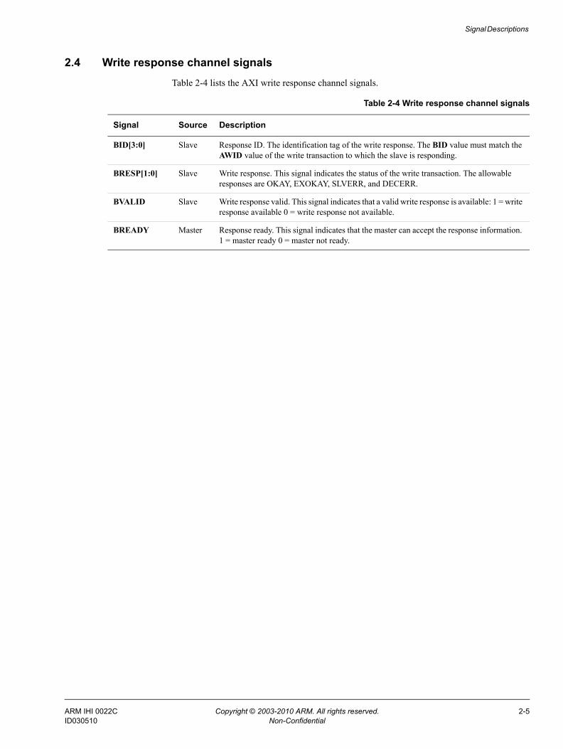
2.4 Write response channel signalsTable 2-4 lists the AXI write response channel signals.
Table 2-4 Write response channel signals
Signal Source Description
BID[3:0] Slave Response ID. The identification tag of the write response. The BID value must match the AWID value of the write transaction to which the slave is responding.
BRESP[1:0] Slave Write response. This signal indicates the status of the write transaction. The allowable responses are OKAY, EXOKAY, SLVERR, and DECERR.
BVALID Slave Write response valid. This signal indicates that a valid write response is available: 1 = write response available 0 = write response not available.
BREADY Master Response ready. This signal indicates that the master can accept the response information. 1 = master ready 0 = master not ready.
ARM IHI 0022C Copyright © 2003-2010 ARM. All rights reserved. 2-5ID030510 Non-Confidential
Signal Descriptions
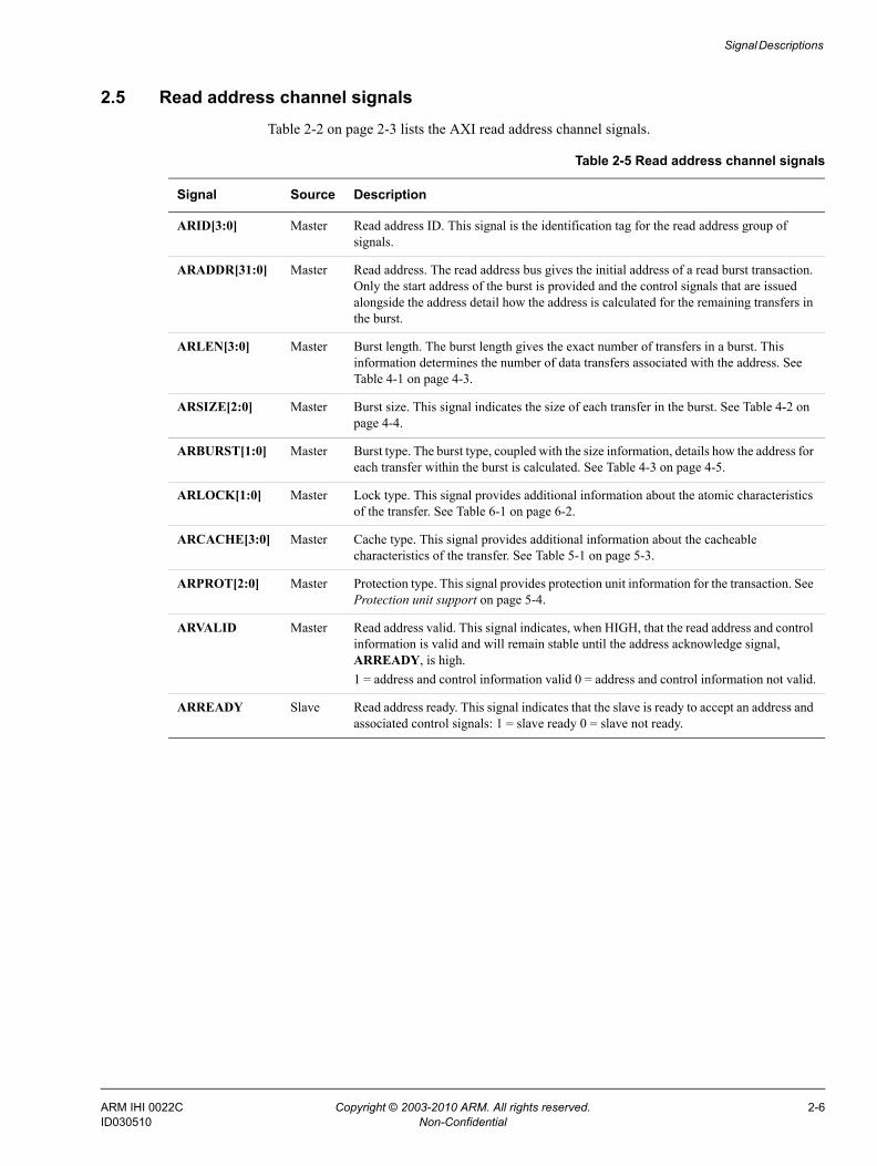
2.5 Read address channel signalsTable 2-2 on page 2-3 lists the AXI read address channel signals.
Table 2-5 Read address channel signals
Signal Source Description
ARID[3:0] Master Read address ID. This signal is the identification tag for the read address group of signals.
ARADDR[31:0] Master Read address. The read address bus gives the initial address of a read burst transaction. Only the start address of the burst is provided and the control signals that are issued alongside the address detail how the address is calculated for the remaining transfers in the burst.
ARLEN[3:0] Master Burst length. The burst length gives the exact number of transfers in a burst. This information determines the number of data transfers associated with the address. See Table 4-1 on page 4-3.
ARSIZE[2:0] Master Burst size. This signal indicates the size of each transfer in the burst. See Table 4-2 on page 4-4.
ARBURST[1:0] Master Burst type. The burst type, coupled with the size information, details how the address for each transfer within the burst is calculated. See Table 4-3 on page 4-5.
ARLOCK[1:0] Master Lock type. This signal provides additional information about the atomic characteristics of the transfer. See Table 6-1 on page 6-2.
ARCACHE[3:0] Master Cache type. This signal provides additional information about the cacheable characteristics of the transfer. See Table 5-1 on page 5-3.
ARPROT[2:0] Master Protection type. This signal provides protection unit information for the transaction. See Protection unit support on page 5-4.
ARVALID Master Read address valid. This signal indicates, when HIGH, that the read address and control information is valid and will remain stable until the address acknowledge signal, ARREADY, is high.1 = address and control information valid 0 = address and control information not valid.
ARREADY Slave Read address ready. This signal indicates that the slave is ready to accept an address and associated control signals: 1 = slave ready 0 = slave not ready.
ARM IHI 0022C Copyright © 2003-2010 ARM. All rights reserved. 2-6ID030510 Non-Confidential
Signal Descriptions
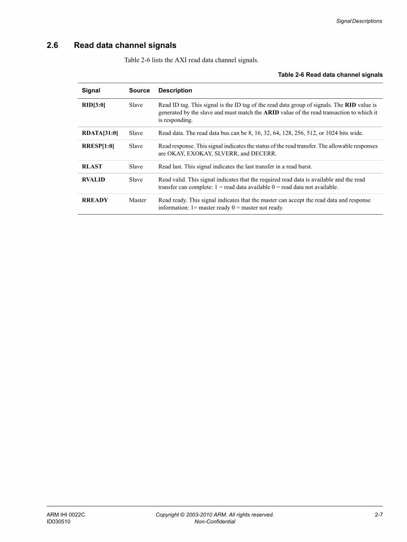
2.6 Read data channel signalsTable 2-6 lists the AXI read data channel signals.
Table 2-6 Read data channel signals
Signal Source Description
RID[3:0] Slave Read ID tag. This signal is the ID tag of the read data group of signals. The RID value is generated by the slave and must match the ARID value of the read transaction to which it is responding.
RDATA[31:0] Slave Read data. The read data bus can be 8, 16, 32, 64, 128, 256, 512, or 1024 bits wide.
RRESP[1:0] Slave Read response. This signal indicates the status of the read transfer. The allowable responses are OKAY, EXOKAY, SLVERR, and DECERR.
RLAST Slave Read last. This signal indicates the last transfer in a read burst.
RVALID Slave Read valid. This signal indicates that the required read data is available and the read transfer can complete: 1 = read data available 0 = read data not available.
RREADY Master Read ready. This signal indicates that the master can accept the read data and response information: 1= master ready 0 = master not ready.
ARM IHI 0022C Copyright © 2003-2010 ARM. All rights reserved. 2-7ID030510 Non-Confidential
Signal Descriptions
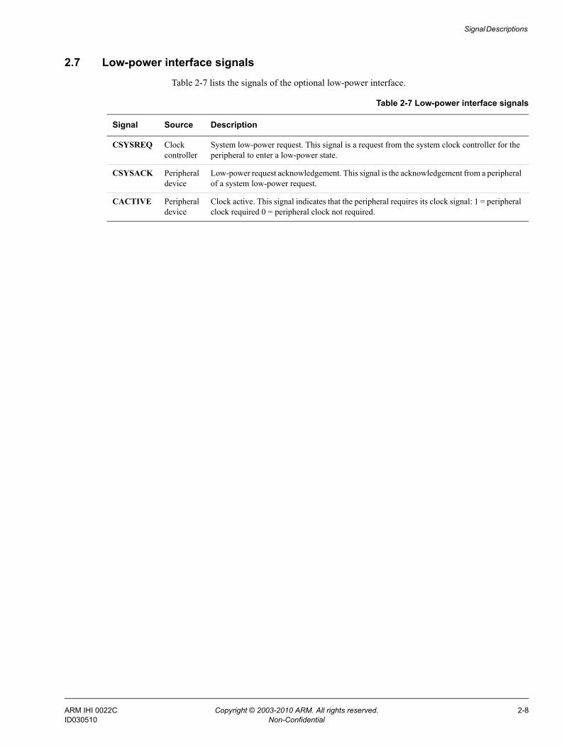
2.7 Low-power interface signalsTable 2-7 lists the signals of the optional low-power interface.
Table 2-7 Low-power interface signals
Signal Source Description
CSYSREQ Clock controller
System low-power request. This signal is a request from the system clock controller for the peripheral to enter a low-power state.
CSYSACK Peripheral device
Low-power request acknowledgement. This signal is the acknowledgement from a peripheral of a system low-power request.
CACTIVE Peripheral device
Clock active. This signal indicates that the peripheral requires its clock signal: 1 = peripheral clock required 0 = peripheral clock not required.
ARM IHI 0022C Copyright © 2003-2010 ARM. All rights reserved. 2-8ID030510 Non-Confidential
Chapter 3 Channel Handshake
This chapter describes the master/slave handshake process and outlines the relationships and default values of the READY and VALID handshake signals. It contains the following sections:• Handshake process on page 3-2• Relationships between the channels on page 3-5• Dependencies between channel handshake signals on page 3-6.
ARM IHI 0022C Copyright © 2003-2010 ARM. All rights reserved. 3-1ID030510 Non-Confidential
Channel Handshake
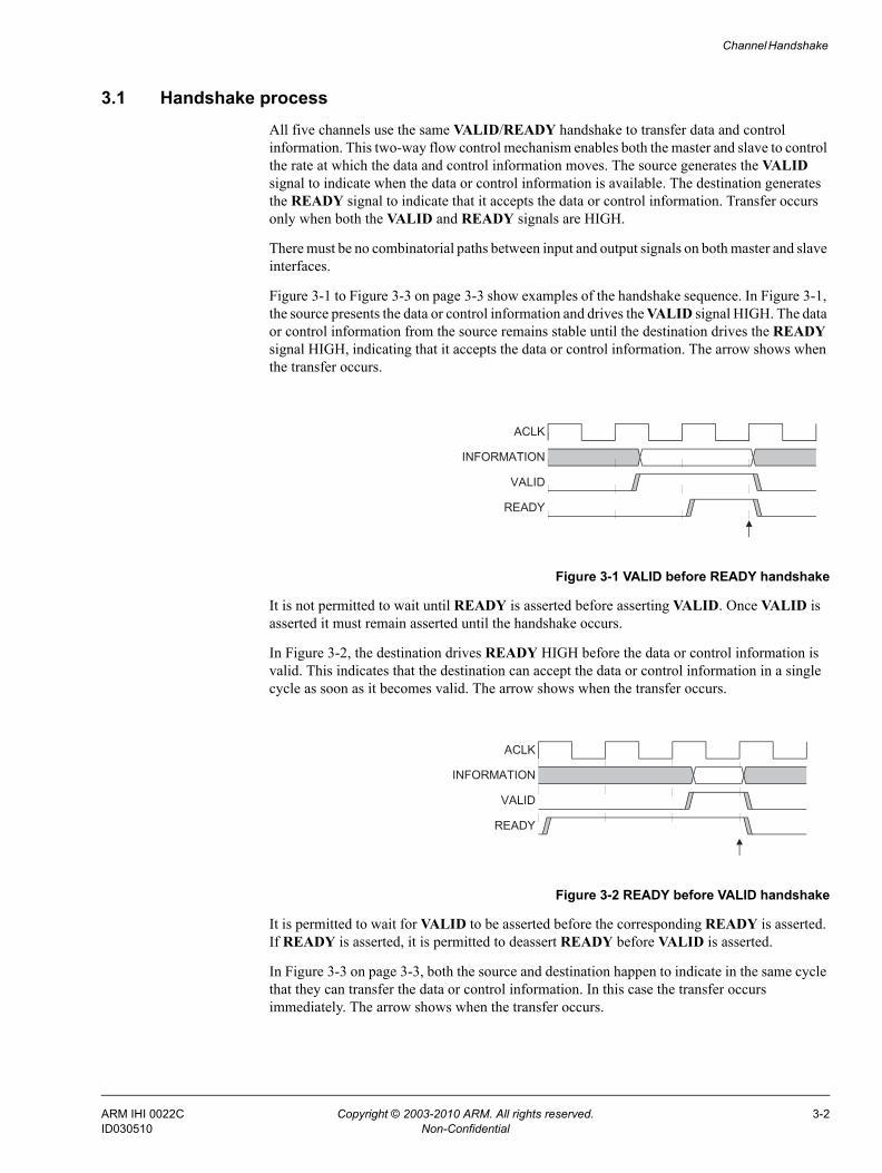
3.1 Handshake processAll five channels use the same VALID/READY handshake to transfer data and control information. This two-way flow control mechanism enables both the master and slave to control the rate at which the data and control information moves. The source generates the VALID signal to indicate when the data or control information is available. The destination generates the READY signal to indicate that it accepts the data or control information. Transfer occurs only when both the VALID and READY signals are HIGH.
There must be no combinatorial paths between input and output signals on both master and slave interfaces.
Figure 3-1 to Figure 3-3 on page 3-3 show examples of the handshake sequence. In Figure 3-1, the source presents the data or control information and drives the VALID signal HIGH. The data or control information from the source remains stable until the destination drives the READY signal HIGH, indicating that it accepts the data or control information. The arrow shows when the transfer occurs.
Figure 3-1 VALID before READY handshake
It is not permitted to wait until READY is asserted before asserting VALID. Once VALID is asserted it must remain asserted until the handshake occurs.
In Figure 3-2, the destination drives READY HIGH before the data or control information is valid. This indicates that the destination can accept the data or control information in a single cycle as soon as it becomes valid. The arrow shows when the transfer occurs.
Figure 3-2 READY before VALID handshake
It is permitted to wait for VALID to be asserted before the corresponding READY is asserted. If READY is asserted, it is permitted to deassert READY before VALID is asserted.
In Figure 3-3 on page 3-3, both the source and destination happen to indicate in the same cycle that they can transfer the data or control information. In this case the transfer occurs immediately. The arrow shows when the transfer occurs.
READY
VALID
INFORMATION
ACLK
READY
VALID
INFORMATION
ACLK
ARM IHI 0022C Copyright © 2003-2010 ARM. All rights reserved. 3-2ID030510 Non-Confidential
Channel Handshake
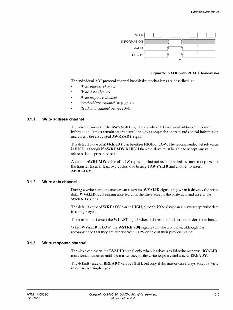
Figure 3-3 VALID with READY handshake
The individual AXI protocol channel handshake mechanisms are described in:• Write address channel• Write data channel• Write response channel• Read address channel on page 3-4• Read data channel on page 3-4.
3.1.1 Write address channel
The master can assert the AWVALID signal only when it drives valid address and control information. It must remain asserted until the slave accepts the address and control information and asserts the associated AWREADY signal.
The default value of AWREADY can be either HIGH or LOW. The recommended default value is HIGH, although if AWREADY is HIGH then the slave must be able to accept any valid address that is presented to it.
A default AWREADY value of LOW is possible but not recommended, because it implies that the transfer takes at least two cycles, one to assert AWVALID and another to assert AWREADY.
3.1.2 Write data channel
During a write burst, the master can assert the WVALID signal only when it drives valid write data. WVALID must remain asserted until the slave accepts the write data and asserts the WREADY signal.
The default value of WREADY can be HIGH, but only if the slave can always accept write data in a single cycle.
The master must assert the WLAST signal when it drives the final write transfer in the burst.
When WVALID is LOW, the WSTRB[3:0] signals can take any value, although it is recommended that they are either driven LOW or held at their previous value.
3.1.3 Write response channel
The slave can assert the BVALID signal only when it drives a valid write response. BVALID must remain asserted until the master accepts the write response and asserts BREADY.
The default value of BREADY can be HIGH, but only if the master can always accept a write response in a single cycle.
READY
VALID
INFORMATION
ACLK
ARM IHI 0022C Copyright © 2003-2010 ARM. All rights reserved. 3-3ID030510 Non-Confidential
Channel Handshake
3.1.4 Read address channel
The master can assert the ARVALID signal only when it drives valid address and control information. It must remain asserted until the slave accepts the address and control information and asserts the associated ARREADY signal.
The default value of ARREADY can be either HIGH or LOW. The recommended default value is HIGH, although if ARREADY is HIGH then the slave must be able to accept any valid address that is presented to it.
A default ARREADY value of LOW is possible but not recommended, because it implies that the transfer takes at least two cycles, one to assert ARVALID and another to assert ARREADY.
3.1.5 Read data channel
The slave can assert the RVALID signal only when it drives valid read data. RVALID must remain asserted until the master accepts the data and asserts the RREADY signal. Even if a slave has only one source of read data, it must assert the RVALID signal only in response to a request for the data.
The master interface uses the RREADY signal to indicate that it accepts the data. The default value of RREADY can be HIGH, but only if the master is able to accept read data immediately, whenever it performs a read transaction.
The slave must assert the RLAST signal when it drives the final read transfer in the burst.
ARM IHI 0022C Copyright © 2003-2010 ARM. All rights reserved. 3-4ID030510 Non-Confidential
Channel Handshake
3.2 Relationships between the channelsThe relationship between the address, read, write, and write response channels is flexible.
For example, the write data can appear at an interface before the write address that relates to it. This can occur when the write address channel contains more register stages than the write data channel. It is also possible for the write data to appear in the same cycle as the address.
When the interconnect must determine the destination address space or slave space, it must realign the address and write data. This is required to assure that the write data is signaled as valid only to the slave for which it is destined.
Two relationships that must be maintained are:
• read data must always follow the address to which the data relates
• a write response must always follow the last write transfer in the write transaction to which the write response relates.
ARM IHI 0022C Copyright © 2003-2010 ARM. All rights reserved. 3-5ID030510 Non-Confidential
Channel Handshake
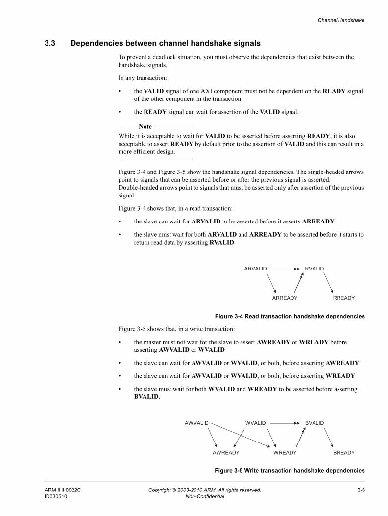
3.3 Dependencies between channel handshake signalsTo prevent a deadlock situation, you must observe the dependencies that exist between the handshake signals.
In any transaction:
• the VALID signal of one AXI component must not be dependent on the READY signal of the other component in the transaction
• the READY signal can wait for assertion of the VALID signal.
Note While it is acceptable to wait for VALID to be asserted before asserting READY, it is also acceptable to assert READY by default prior to the assertion of VALID and this can result in a more efficient design.
Figure 3-4 and Figure 3-5 show the handshake signal dependencies. The single-headed arrows point to signals that can be asserted before or after the previous signal is asserted. Double-headed arrows point to signals that must be asserted only after assertion of the previous signal.
Figure 3-4 shows that, in a read transaction:
• the slave can wait for ARVALID to be asserted before it asserts ARREADY
• the slave must wait for both ARVALID and ARREADY to be asserted before it starts to return read data by asserting RVALID.
Figure 3-4 Read transaction handshake dependencies
Figure 3-5 shows that, in a write transaction:
• the master must not wait for the slave to assert AWREADY or WREADY before asserting AWVALID or WVALID
• the slave can wait for AWVALID or WVALID, or both, before asserting AWREADY
• the slave can wait for AWVALID or WVALID, or both, before asserting WREADY
• the slave must wait for both WVALID and WREADY to be asserted before asserting BVALID.
Figure 3-5 Write transaction handshake dependencies
ARVALID
ARREADY
RVALID
RREADY
WREADY
AWVALID
AWREADY
WVALID BVALID
BREADY
ARM IHI 0022C Copyright © 2003-2010 ARM. All rights reserved. 3-6ID030510 Non-Confidential

Channel Handshake
Note It is important that during a write transaction, a master must not wait for AWREADY to be asserted before driving WVALID. This could cause a deadlock condition if the slave is conversely waiting for WVALID before asserting AWREADY.
ARM IHI 0022C Copyright © 2003-2010 ARM. All rights reserved. 3-7ID030510 Non-Confidential
Chapter 4 Addressing Options
This chapter describes AXI burst types and how to calculate addresses and byte lanes for transfers within a burst. It contains the following sections:• About addressing options on page 4-2• Burst length on page 4-3• Burst size on page 4-4• Burst type on page 4-5• Burst address on page 4-7.
ARM IHI 0022C Copyright © 2003-2010 ARM. All rights reserved. 4-1ID030510 Non-Confidential
Addressing Options
4.1 About addressing optionsThe AXI protocol is burst-based, and the master begins each burst by driving transfer control information and the address of the first byte in the transfer. As the burst transaction progresses, it is the responsibility of the slave to calculate the addresses of subsequent transfers in the burst.
Bursts must not cross 4KB boundaries to prevent them from crossing boundaries between slaves and to limit the size of the address incrementer required within slaves.
ARM IHI 0022C Copyright © 2003-2010 ARM. All rights reserved. 4-2ID030510 Non-Confidential
Addressing Options
4.2 Burst lengthThe AWLEN or ARLEN signal specifies the number of data transfers that occur within each burst. As Table 4-1 shows, each burst can be 1-16 transfers long.
For wrapping bursts, the length of the burst must be 2, 4, 8, or 16 transfers.
Every transaction must have the number of transfers specified by ARLEN or AWLEN. No component can terminate a burst early to reduce the number of data transfers. During a write burst, the master can disable further writing by deasserting all the write strobes, but it must complete the remaining transfers in the burst. During a read burst, the master can discard further read data, but it must complete the remaining transfers in the burst.
Caution Discarding read data that is not required can result in lost data when accessing a read-sensitive device such as a FIFO. A master must never access such a device using a burst length longer than required.
Table 4-1 Burst length encoding
ARLEN[3:0]AWLEN[3:0]
Number ofdata transfers
b0000 1
b0001 2
b0010 3
. . .
b1101 14
b1110 15
b1111 16
ARM IHI 0022C Copyright © 2003-2010 ARM. All rights reserved. 4-3ID030510 Non-Confidential
Addressing Options
4.3 Burst sizeTable 4-2 shows how the ARSIZE or AWSIZE signal specifies the maximum number of data bytes to transfer in each beat, or data transfer, within a burst.
The AXI determines from the transfer address which byte lanes of the data bus to use for each transfer.
For incrementing or wrapping bursts with transfer sizes narrower than the data bus, data transfers are on different byte lanes for each beat of the burst. The address of a fixed burst remains constant, and every transfer uses the same byte lanes.
The size of any transfer must not exceed the data bus width of the components in the transaction.
Table 4-2 Burst size encoding
ARSIZE[2:0]AWSIZE[2:0]
Bytes intransfer
b000 1
b001 2
b010 4
b011 8
b100 16
b101 32
b110 64
b111 128
ARM IHI 0022C Copyright © 2003-2010 ARM. All rights reserved. 4-4ID030510 Non-Confidential
Addressing Options
4.4 Burst typeThe AXI protocol defines three burst types described in:• Fixed burst• Incrementing burst• Wrapping burst on page 4-6.
Table 4-3 shows how the ARBURST or AWBURST signal selects the burst type.
4.4.1 Fixed burst
In a fixed burst, the address remains the same for every transfer in the burst. This burst type is for repeated accesses to the same location such as when loading or emptying a peripheral FIFO.
4.4.2 Incrementing burst
In an incrementing burst, the address for each transfer in the burst is an increment of the previous transfer address. The increment value depends on the size of the transfer. For example, the address for each transfer in a burst with a size of four bytes is the previous address plus four.
Table 4-3 Burst type encoding
ARBURST[1:0]AWBURST[1:0]
Burst type Description Access
b00 FIXED Fixed-address burst FIFO-type
b01 INCR Incrementing-address burst Normal sequential memory
b10 WRAP Incrementing-address burst that wraps to a lower address at the wrap boundary
Cache line
b11 Reserved - -
ARM IHI 0022C Copyright © 2003-2010 ARM. All rights reserved. 4-5ID030510 Non-Confidential
Addressing Options
4.4.3 Wrapping burst
A wrapping burst is similar to an incrementing burst, in that the address for each transfer in the burst is an increment of the previous transfer address. However, in a wrapping burst the address wraps around to a lower address when a wrap boundary is reached. The wrap boundary is the size of each transfer in the burst multiplied by the total number of transfers in the burst.
Two restrictions apply to wrapping bursts:• the start address must be aligned to the size of the transfer• the length of the burst must be 2, 4, 8, or 16.
ARM IHI 0022C Copyright © 2003-2010 ARM. All rights reserved. 4-6ID030510 Non-Confidential
Addressing Options
4.5 Burst addressThis section provides some simple formulas for determining the address and byte lanes of transfers within a burst. The formulas use the following variables:
Start_Address The start address issued by the master.
Number_Bytes The maximum number of bytes in each data transfer.
Data_Bus_Bytes The number of byte lanes in the data bus.
Aligned_Address The aligned version of the start address.
Burst_Length The total number of data transfers within a burst.
Address_N The address of transfer N within a burst. N is an integer from 2-16.
Wrap_Boundary The lowest address within a wrapping burst.
Lower_Byte_Lane The byte lane of the lowest addressed byte of a transfer.
Upper_Byte_Lane The byte lane of the highest addressed byte of a transfer.
INT(x) The rounded-down integer value of x.
Use these equations to determine addresses of transfers within a burst:• Start_Address = ADDR• Number_Bytes = 2SIZE
• Burst_Length = LEN + 1• Aligned_Address = (INT(Start_Address / Number_Bytes) ) x Number_Bytes.
Use this equation to determine the address of the first transfer in a burst:• Address_1 = Start_Address.
Use this equation to determine the address of any transfer after the first transfer in a burst:• Address_N = Aligned_Address + (N – 1) x Number_Bytes.
For wrapping bursts, the Wrap_Boundary variable is used to account for the wrapping boundary:• Wrap_Boundary = (INT(Start_Address / (Number_Bytes x Burst_Length)))
x (Number_Bytes x Burst_Length).
If Address_N = Wrap_Boundary + (Number_Bytes x Burst_Length), use this equation:• Address_N = Wrap_Boundary.
After the wrapping boundary, use this equation:
• Address_N = Start_Address + ((N – 1) x Number_Bytes) - (Number_Bytes x Burst_Length).
Use these equations to determine which byte lanes to use for the first transfer in a burst:• Lower_Byte_Lane = Start_Address - (INT(Start_Address / Data_Bus_Bytes))
x Data_Bus_Bytes
• Upper_Byte_Lane = Aligned_Address + (Number_Bytes - 1) - (INT(Start_Address / Data_Bus_Bytes)) x Data_Bus_Bytes.
Use these equations to determine which byte lanes to use for all transfers after the first transfer in a burst:
• Lower_Byte_Lane = Address_N – (INT(Address_N / Data_Bus_Bytes)) x Data_Bus_Bytes
• Upper_Byte_Lane = Lower_Byte_Lane + Number_Bytes – 1.
ARM IHI 0022C Copyright © 2003-2010 ARM. All rights reserved. 4-7ID030510 Non-Confidential

Addressing Options
Data is transferred on:• DATA[(8 x Upper_Byte_Lane) + 7 : (8 x Lower_Byte_Lane)].
ARM IHI 0022C Copyright © 2003-2010 ARM. All rights reserved. 4-8ID030510 Non-Confidential
Chapter 5 Additional Control Information
This chapter describes AXI protocol support for system-level caches and protection units. It contains the following sections:• Cache support on page 5-2• Protection unit support on page 5-4.
ARM IHI 0022C Copyright © 2003-2010 ARM. All rights reserved. 5-1ID030510 Non-Confidential
Additional Control Information
5.1 Cache supportSupport for system level caches and other performance enhancing components is provided by the use of the cache information signals, ARCACHE and AWCACHE. These signals provide additional information about how the transaction can be processed.
The ARCACHE[3:0] or AWCACHE[3:0] signal supports system-level caches by providing the bufferable, cacheable, and allocate attributes of the transaction:
Bufferable (B) bit, ARCACHE[0] and AWCACHE[0] When this bit is HIGH, it means that the interconnect or any component can delay the transaction reaching its final destination for an arbitrary number of cycles. This is usually only relevant to writes.
Cacheable (C) bit, ARCACHE[1] and AWCACHE[1] When this bit is HIGH, it means that the transaction at the final destination does not have to match the characteristics of the original transaction.For writes this means that a number of different writes can be merged together.For reads this means that a location can be pre-fetched or can be fetched just once for multiple read transactions.To determine if a transaction should be cached this bit should be used in conjunction with the Read Allocate (RA) and Write Allocate (WA) bits.
Read Allocate (RA) bit, ARCACHE[2] and AWCACHE[2] When the RA bit is HIGH, it means that if the transfer is a read and it misses in the cache then it should be allocated.The RA bit must not be HIGH if the C bit is low.
Write Allocate (WA) bit, ARCACHE[3] and AWCACHE[3] When the WA bit is HIGH, it means that if the transfer is a write and it misses in the cache then it should be allocated.The WA bit must not be HIGH if the C bit is low.
ARM IHI 0022C Copyright © 2003-2010 ARM. All rights reserved. 5-2ID030510 Non-Confidential
Additional Control Information
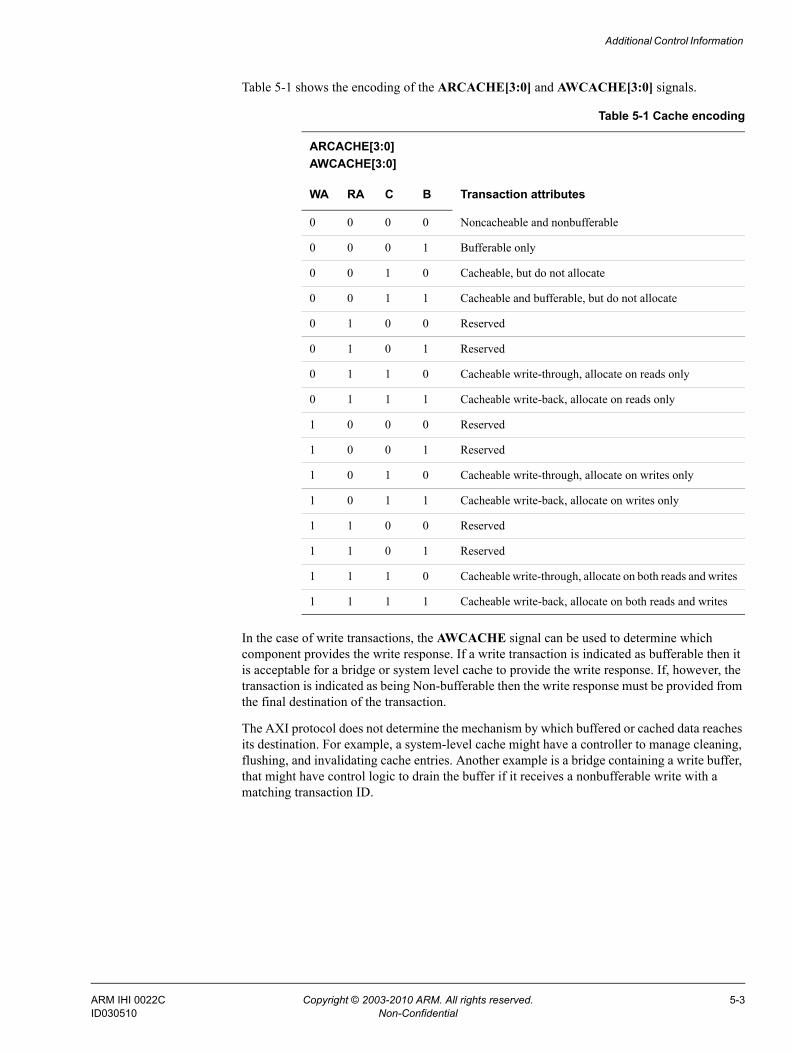
Table 5-1 shows the encoding of the ARCACHE[3:0] and AWCACHE[3:0] signals.
In the case of write transactions, the AWCACHE signal can be used to determine which component provides the write response. If a write transaction is indicated as bufferable then it is acceptable for a bridge or system level cache to provide the write response. If, however, the transaction is indicated as being Non-bufferable then the write response must be provided from the final destination of the transaction.
The AXI protocol does not determine the mechanism by which buffered or cached data reaches its destination. For example, a system-level cache might have a controller to manage cleaning, flushing, and invalidating cache entries. Another example is a bridge containing a write buffer, that might have control logic to drain the buffer if it receives a nonbufferable write with a matching transaction ID.
Table 5-1 Cache encoding
ARCACHE[3:0]AWCACHE[3:0]
Transaction attributesWA RA C B
0 0 0 0 Noncacheable and nonbufferable
0 0 0 1 Bufferable only
0 0 1 0 Cacheable, but do not allocate
0 0 1 1 Cacheable and bufferable, but do not allocate
0 1 0 0 Reserved
0 1 0 1 Reserved
0 1 1 0 Cacheable write-through, allocate on reads only
0 1 1 1 Cacheable write-back, allocate on reads only
1 0 0 0 Reserved
1 0 0 1 Reserved
1 0 1 0 Cacheable write-through, allocate on writes only
1 0 1 1 Cacheable write-back, allocate on writes only
1 1 0 0 Reserved
1 1 0 1 Reserved
1 1 1 0 Cacheable write-through, allocate on both reads and writes
1 1 1 1 Cacheable write-back, allocate on both reads and writes
ARM IHI 0022C Copyright © 2003-2010 ARM. All rights reserved. 5-3ID030510 Non-Confidential
Additional Control Information
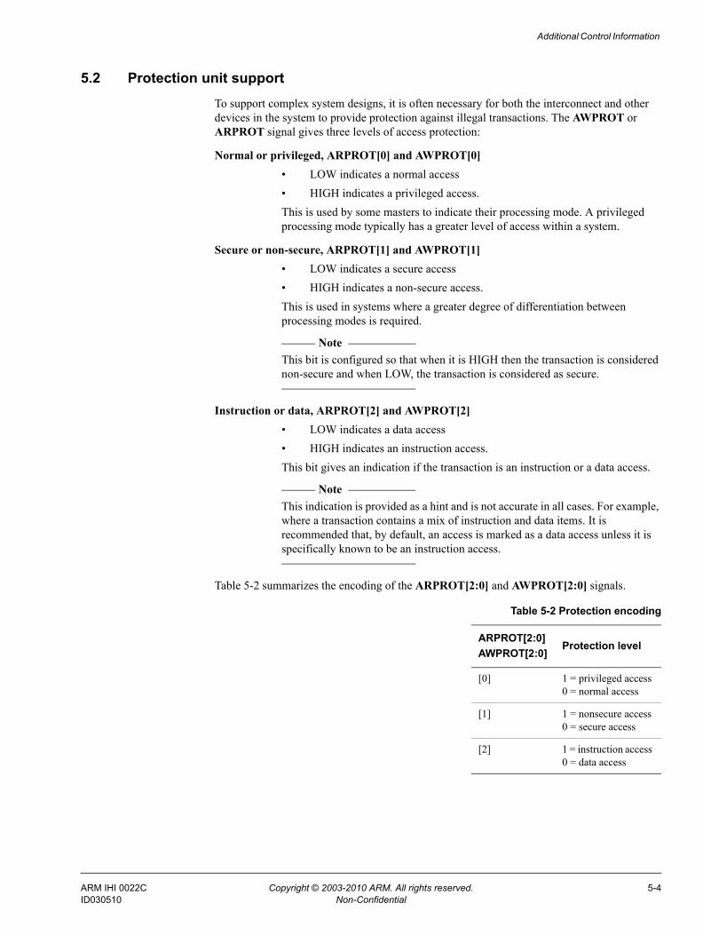
5.2 Protection unit supportTo support complex system designs, it is often necessary for both the interconnect and other devices in the system to provide protection against illegal transactions. The AWPROT or ARPROT signal gives three levels of access protection:
Normal or privileged, ARPROT[0] and AWPROT[0] • LOW indicates a normal access• HIGH indicates a privileged access.This is used by some masters to indicate their processing mode. A privileged processing mode typically has a greater level of access within a system.
Secure or non-secure, ARPROT[1] and AWPROT[1] • LOW indicates a secure access• HIGH indicates a non-secure access.This is used in systems where a greater degree of differentiation between processing modes is required.
Note This bit is configured so that when it is HIGH then the transaction is considered
non-secure and when LOW, the transaction is considered as secure.
Instruction or data, ARPROT[2] and AWPROT[2] • LOW indicates a data access• HIGH indicates an instruction access.This bit gives an indication if the transaction is an instruction or a data access.
Note This indication is provided as a hint and is not accurate in all cases. For example,
where a transaction contains a mix of instruction and data items. It is recommended that, by default, an access is marked as a data access unless it is specifically known to be an instruction access.
Table 5-2 summarizes the encoding of the ARPROT[2:0] and AWPROT[2:0] signals.
Table 5-2 Protection encoding
ARPROT[2:0]AWPROT[2:0]
Protection level
[0] 1 = privileged access 0 = normal access
[1] 1 = nonsecure access 0 = secure access
[2] 1 = instruction access 0 = data access
ARM IHI 0022C Copyright © 2003-2010 ARM. All rights reserved. 5-4ID030510 Non-Confidential
Chapter 6 Atomic Accesses
This chapter describes how the AXI protocol implements exclusive access and locked access mechanisms. It contains the following sections:• About atomic accesses on page 6-2• Exclusive access on page 6-3• Locked access on page 6-6.
ARM IHI 0022C Copyright © 2003-2010 ARM. All rights reserved. 6-1ID030510 Non-Confidential
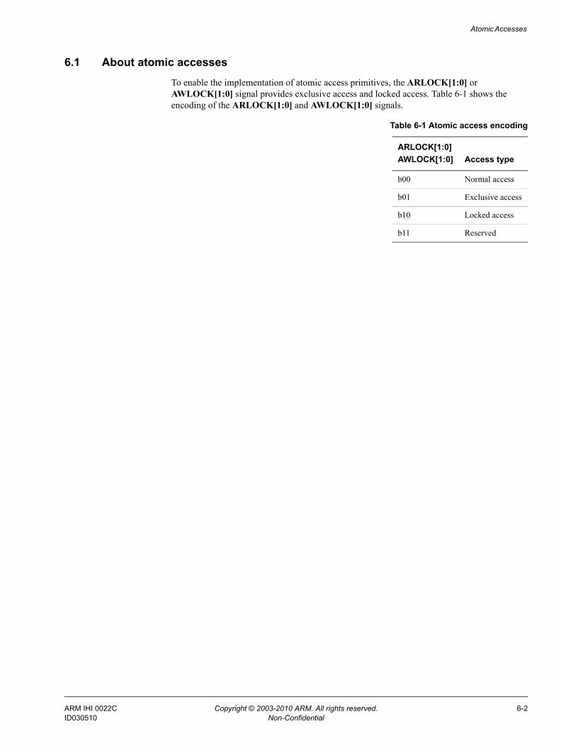
Atomic Accesses
6.1 About atomic accessesTo enable the implementation of atomic access primitives, the ARLOCK[1:0] or AWLOCK[1:0] signal provides exclusive access and locked access. Table 6-1 shows the encoding of the ARLOCK[1:0] and AWLOCK[1:0] signals.
Table 6-1 Atomic access encoding
ARLOCK[1:0]AWLOCK[1:0] Access type
b00 Normal access
b01 Exclusive access
b10 Locked access
b11 Reserved
ARM IHI 0022C Copyright © 2003-2010 ARM. All rights reserved. 6-2ID030510 Non-Confidential
Atomic Accesses
6.2 Exclusive accessThe exclusive access mechanism enables the implementation of semaphore type operations without requiring the bus to remain locked to a particular master for the duration of the operation. The advantage of exclusive access is that semaphore type operations do not impact either the critical bus access latency or the maximum achievable bandwidth.
The ARLOCK[1:0] or AWLOCK[1:0] signal selects exclusive access, and the RRESP[1:0] or BRESP[1:0] signal (see Table 7-1 on page 7-2) indicates the success or failure of the exclusive access.
The slave must have additional logic to support exclusive access. The AXI protocol provides a fail-safe mechanism to indicate when a master attempts an exclusive access to a slave that does not support it.
6.2.1 Exclusive access process
The basic process for an exclusive access is:
1. A master performs an exclusive read from an address location.
2. At some later time, the master attempts to complete the exclusive operation by performing an exclusive write to the same address location.
3. The exclusive write access of the master is signalled as:• Successful if no other master has written to that location between the read and write
accesses.• Failed if another master has written to that location between the read and write
accesses. In this case the address location is not updated.
Note A master might not complete the write portion of an exclusive operation. The exclusive
access monitoring hardware must monitor only one address per transaction ID. Therefore, if a master does not complete the write portion of an exclusive operation, a subsequent exclusive read changes the address that is being monitored for exclusivity.
6.2.2 Exclusive access from the perspective of the master
A master starts an exclusive operation by performing an exclusive read. This usually returns the EXOKAY response from the slave, indicating that the slave recorded the address to be monitored.
Note If the master attempts an exclusive read from a slave that does not support exclusive accesses, the slave returns the OKAY response instead of the EXOKAY response. The master can treat this as an error condition indicating that the exclusive access is not supported. It is recommended that the master not perform the write portion of this exclusive operation.
At some time after the exclusive read, the master tries an exclusive write to the same location. If the location has not changed since the exclusive read, the exclusive write operation succeeds. The slave returns the EXOKAY response, and the exclusive write updates the memory location.
If the address location has changed since the exclusive read, the exclusive write attempt fails, and the slave returns the OKAY response instead of the EXOKAY response. The exclusive write attempt does not update the memory location.
ARM IHI 0022C Copyright © 2003-2010 ARM. All rights reserved. 6-3ID030510 Non-Confidential
Atomic Accesses
A master might not complete the write portion of an exclusive operation. If this happens, the slave continues to monitor the address for exclusivity until another exclusive read initiates a new exclusive access.
A master must not commence the write portion of an exclusive access until the read portion is complete.
6.2.3 Exclusive access from the perspective of the slave
A slave that is not capable of supporting exclusive accesses can ignore the ARLOCK[1:0] and AWLOCK[1:0] signals. It must provide an OKAY response for both normal and exclusive accesses.
A slave that supports exclusive access must have monitor hardware. It is recommended that such a slave has a monitor unit for each exclusive-capable master ID that can access it. A single-ported slave can have a standard exclusive access monitor external to the slave, but multiported slaves might require internal monitoring.
The exclusive access monitor records the address and ARID value of any exclusive read operation. Then it monitors that location until either a write occurs to that location or until another exclusive read with the same ARID value resets the monitor to a different address.
When an exclusive write occurs with a given AWID value then the monitor checks to see if that address is being monitored for exclusivity. If it is, then this implies that no write has occurred to that location, and the exclusive write proceeds, completing the exclusive access. The slave returns the EXOKAY response to the master.
If the address is no longer being monitored at the time of an exclusive write, this implies one of the following:• the location has been updated since the exclusive read• the monitor has been reset to another location.
In both cases the exclusive write must not update the address location, and the slave must return the OKAY response instead of the EXOKAY response.
6.2.4 Exclusive access restrictions
The following restrictions apply to exclusive accesses:
• The size and length of an exclusive write with a given ID must be the same as the size and length of the preceding exclusive read with the same ID.
• The address of an exclusive access must be aligned to the total number of bytes in the transaction.
• The address for the exclusive read and the exclusive write must be identical.
• The ARID field of the read portion of the exclusive access must match the AWID of the write portion.
• The control signals for the read and write portions of the exclusive access must be identical.
• The number of bytes to be transferred in an exclusive access burst must be a power of 2, that is, 1, 2, 4, 8, 16, 32, 64, or 128 bytes.
• The maximum number of bytes that can be transferred in an exclusive burst is 128.
ARM IHI 0022C Copyright © 2003-2010 ARM. All rights reserved. 6-4ID030510 Non-Confidential
Atomic Accesses
• The value of the ARCACHE[3:0] or AWCACHE[3:0] signals must guarantee that the slave that is monitoring the exclusive access sees the transaction. For example, an exclusive access being monitored by a slave must not have an ARCACHE[3:0] or AWCACHE[3:0] value that indicates that the transaction is cacheable.
Failure to observe these restrictions causes Unpredictable behavior.
The minimum number of bytes to be monitored during an exclusive operation is defined by the length and size of the transaction. It is acceptable to monitor a larger number of bytes, up to 128 which is the maximum of an exclusive access. However, this might result in occasions when the exclusive access is actually successful but is indicated as failing because a neighboring byte was updated.
6.2.5 Slaves that do not support exclusive access
The response signals, BRESP[1:0] and RRESP[1:0], include an OKAY response for successful normal accesses and an EXOKAY response for successful exclusive accesses. This means that a slave that does not support exclusive accesses can provide an OKAY response to indicate the failure of an exclusive access.
Note An exclusive write to a slave that does not support exclusive access always updates the memory location.
An exclusive write to a slave that supports exclusive access updates the memory location only if the exclusive write is successful.
ARM IHI 0022C Copyright © 2003-2010 ARM. All rights reserved. 6-5ID030510 Non-Confidential
Atomic Accesses
6.3 Locked accessWhen the ARLOCK[1:0] or AWLOCK[1:0] signals for a transaction show that it is a locked transfer then the interconnect must ensure that only that master is allowed access to the slave region until an unlocked transfer from the same master completes. The arbiter within the interconnect is used to enforce this restriction.
When a master starts a locked sequence of either read or write transactions it must ensure that it has no other outstanding transactions waiting to complete.
Any transaction with ARLOCK[1:0] or AWLOCK[1:0] set to indicate a locked sequence forces the interconnect to lock the following transaction. Therefore, a locked sequence must always complete with a final transaction that does not have ARLOCK[1:0] or AWLOCK[1:0] set to indicate a locked access. This final transaction is included in the locked sequence and effectively removes the lock.
When completing a locked sequence a master must ensure that all previous locked transactions are complete before issuing the final unlocking transaction. It must then ensure that the final unlocking transaction has fully completed before any further transactions are commenced.
The master must ensure that all transactions within a locked sequence have the same ARID or AWID value.
Note Locked accesses require that the interconnect prevents any other transactions occurring while the locked sequence is in progress and can therefore have an impact on the interconnect performance. It is recommended that locked accesses are only used to support legacy devices.
The following restrictions are recommended but not mandatory:• keep all locked transaction sequences within the same 4KB address region• limit locked transaction sequences to two transactions.
ARM IHI 0022C Copyright © 2003-2010 ARM. All rights reserved. 6-6ID030510 Non-Confidential
Chapter 7 Response Signaling
This chapter describes the four slave responses in AXI read and write transactions. It contains the following sections:• About response signaling on page 7-2• Response types on page 7-3.
ARM IHI 0022C Copyright © 2003-2010 ARM. All rights reserved. 7-1ID030510 Non-Confidential
Response Signaling
7.1 About response signalingThe AXI protocol allows response signaling for both read and write transactions. For read transactions the response information from the slave is passed alongside the read data itself, however for writes the response information is conveyed along the write response channel.
The AXI protocol responses are:• OKAY • EXOKAY • SLVERR • DECERR.
Table 7-1 shows the encoding of the RRESP[1:0] and BRESP[1:0] signals.
For a write transaction, there is just one response given for the entire burst and not for each data transfer within the burst.
In a read transaction, the slave can give different responses for different transfers within a burst. In a burst of 16 read transfers, for example, the slave might return an OKAY response for 15 of the transfers and a SLVERR response for one of the transfers.
The protocol defines that the required number of data transfers must be performed, even if an error is reported. For example, if a read of 8 transfers is requested from a slave but the slave has an error condition then the slave must perform 8 data transfers, each with an error response. The remainder of the burst is not cancelled if the slave gives a single error response.
This protocol places restrictions on masters that can issue multiple outstanding addresses and that must also support precise error signaling. Such masters must be able to handle an error response for an earlier transfer while later transfers are already underway.
Table 7-1 RRESP[1:0] and BRESP[1:0] encoding
RRESP[1:0] BRESP[1:0] Response Meaning
b00 OKAY Normal access okay indicates if a normal access has been successful. Can also indicate an exclusive access failure.
b01 EXOKAY Exclusive access okay indicates that either the read or write portion of an exclusive access has been successful.
b10 SLVERR Slave error is used when the access has reached the slave successfully, but the slave wishes to return an error condition to the originating master.
b11 DECERR Decode error is generated typically by an interconnect component to indicate that there is no slave at the transaction address.
ARM IHI 0022C Copyright © 2003-2010 ARM. All rights reserved. 7-2ID030510 Non-Confidential
Response Signaling
7.2 Response typesThis section describes the four AXI protocol response types:• Normal access success• Exclusive access• Slave error• Decode error.
7.2.1 Normal access success
The OKAY response indicates:• the success of a normal access• the failure of an exclusive access• an exclusive access to a slave that does not support exclusive access.
OKAY is the response for most transactions.
7.2.2 Exclusive access
The EXOKAY response indicates the success of an exclusive access. Chapter 6 Atomic Accesses describes this response.
7.2.3 Slave error
The SLVERR response indicates an unsuccessful transaction. Examples of slave error conditions are:• FIFO/buffer overrun or underrun condition• unsupported transfer size attempted• write access attempted to read-only location• timeout condition in the slave• access attempted to an address where no registers are present• access attempted to a disabled or powered-down function.
To simplify system monitoring and debugging, it is recommended that error responses are used only for error conditions and not for signaling normal, expected events.
7.2.4 Decode error
In a system without a fully-decoded address map, there can be addresses at which there are no slaves to respond to a transaction. In such a system, the interconnect must provide a suitable error response to flag the access as illegal and also to prevent the system from locking up by trying to access a nonexistent slave.
When the interconnect cannot successfully decode a slave access, it effectively routes the access to a default slave, and the default slave returns the DECERR response.
An implementation option is to have the default slave also record the details of decode errors for later determination of how the errors occurred. In this way, the default slave can significantly simplify the debugging process.
The AXI protocol requires that all data transfers for a transaction are completed, even if an error condition occurs. Therefore any component giving a DECERR response must meet this requirement.
ARM IHI 0022C Copyright © 2003-2010 ARM. All rights reserved. 7-3ID030510 Non-Confidential
Chapter 8 Ordering Model
This chapter describes how the AXI protocol uses transaction ID tags to enable the issuing of multiple outstanding addresses and out-of-order transaction processing. It contains the following sections:• About the Ordering model on page 8-2• Transfer ID fields on page 8-3• Read ordering on page 8-4• Normal write ordering on page 8-5• Write data interleaving on page 8-6• Read and write interaction on page 8-7• Interconnect use of ID fields on page 8-8• Recommended width of ID fields on page 8-9.
ARM IHI 0022C Copyright © 2003-2010 ARM. All rights reserved. 8-1ID030510 Non-Confidential
Ordering Model
8.1 About the Ordering modelThe AXI protocol enables out-of-order transaction completion and the issuing of multiple outstanding addresses. These features enable the implementation of a high-performance interconnect, maximizing data throughput and system efficiency.
The ID signals support out-of-order transactions by enabling each port to act as multiple ordered ports. All transactions with a given ID must be ordered, but there is no restriction on the ordering of transactions with different IDs. The five transaction IDs are:
AWID The ID tag for the write address group of signals.
WID The write ID tag for a write transaction. Along with the write data, the master transfers a WID to match the AWID of the corresponding address.
BID The ID tag for the write response. The slave transfers a BID to match the AWID and WID of the transaction to which it is responding.
ARID The ID tag for the read address group of signals.
RID The read ID tag for a read transaction. The slave transfers an RID to match the ARID of the transaction to which it is responding.
Note There is no requirement for slaves and masters to use these advanced features. Simple masters and slaves can process one transaction at a time in the order they are issued.
The ability to issue multiple outstanding addresses means that masters can issue transaction addresses without waiting for earlier transactions to complete. This feature can improve system performance because it enables parallel processing of transactions,.
The ability to complete transactions out of order means that transactions to faster memory regions can complete without waiting for earlier transactions to slower memory regions. This feature can also improve system performance because it reduces the effect of transaction latency.
Note The reordering of transactions is always with respect to other transactions. There is no facility for the reordering of data transfers within a burst. The address and control signals that define the burst control the order of transfers within the burst.
ARM IHI 0022C Copyright © 2003-2010 ARM. All rights reserved. 8-2ID030510 Non-Confidential
Ordering Model
8.2 Transfer ID fieldsThe AXI protocol provides an ID field to enable a master to issue a number of separate transactions, each of which must be returned in order.
A master can use the ARID or AWID field of a transaction to provide additional information about the ordering requirements of the master. The rules governing the ordering of transactions are as follows:
• Transactions from different masters have no ordering restrictions. They can complete in any order.
• Transactions from the same master, but with different ID values, have no ordering restrictions. They can complete in any order.
• The data for a sequence of write transactions with the same AWID value must complete in the same order that the master issued the addresses in.
• The data for a sequence of read transactions with the same ARID value must be returned in order that:— when reads with the same ARID are from the same slave then the slave must ensure
that the read data returns in the same order that the addresses are received.— when reads with the same ARID are from different slaves, the interconnect must
ensure that the read data returns in the same order that the master issued the addresses in.
• There are no ordering restrictions between read and write transactions with the same AWID and ARID. If a master requires an ordering restriction then it must ensure that the first transaction is fully completed before the second transaction is issued.
ARM IHI 0022C Copyright © 2003-2010 ARM. All rights reserved. 8-3ID030510 Non-Confidential
Ordering Model
8.3 Read orderingAt a master interface, read data from read transactions with the same ARID value must arrive in the same order in which the master issued the addresses. Data from read transactions with different ARID values can return in any order and it is also acceptable to interleave the read data of transactions with different ARID fields.
A slave must return read data from a sequence of read transactions with the same ARID value in the same order in which it received the addresses. In a sequence of read transactions with different ARID values, the slave can return the read data in a different order than that in which the transactions arrived.
The slave must ensure that the RID value of any returned read data matches the ARID value of the address to which it is responding.
The interconnect must ensure that a sequence of read transactions with the same ARID value from different slaves complete in order.
The read data reordering depth is the number of addresses pending in the slave that can be reordered. A slave that processes all transactions in order has a read data reordering depth of one. The read data reordering depth is a static value that must be specified by the designer of the slave.
ARM IHI 0022C Copyright © 2003-2010 ARM. All rights reserved. 8-4ID030510 Non-Confidential
Ordering Model
8.4 Normal write orderingIf a slave does not support write data interleaving (see Write data interleaving on page 8-6), the master must issue the data of write transactions in the same order in which it issues the transaction addresses.
Most slave designs do not support write data interleaving and consequently these types of slave design must receive write data in the same order that they receive the addresses. If the interconnect combines write transactions from different masters to one slave, it must ensure that it combines the write data in address order.
These restrictions apply even if the write transactions have different AWID values.
ARM IHI 0022C Copyright © 2003-2010 ARM. All rights reserved. 8-5ID030510 Non-Confidential
Ordering Model
8.5 Write data interleavingWrite data interleaving enables a slave interface to accept interleaved write data with different AWID values. The slave declares a write data interleaving depth that indicates if the interface can accept interleaved write data from sources with different AWID values. The write data interleaving depth is statically configured. By default, the write data interleaving depth of any interface is one.
Note It is not permitted to interleave the write data of different transactions that have the same AWID.
The write data interleaving depth is the number of different addresses that are currently pending in the slave interface for which write data can be supplied. For example, a slave with a write data interleaving depth of two that has four different addresses, all with different AWID values, pending can accept data for either of the first two pending addresses.
The order in which a slave receives the first data item of each transaction must be the same as the order in which it receives the addresses for the transactions.
Write data interleaving can prevent stalling when the interconnect combines multiple streams of write data destined for the same slave. The interconnect might combine one write data stream from a slow source and another write data stream from a fast source. By interleaving the two write data streams, the interconnect can improve system performance.
Note If two write transactions with different AWID values access the same or overlapping address locations then the processing order is not defined. A higher-level protocol must ensure the correct order of transaction processing.
A master interface that is capable of generating write data with only one AWID value generates all write data in the same order in which it issues the addresses. However, a master interface can interleave write data with different WID values if the slave interface has a write data interleaving depth greater than one.
For most masters that can internally control the generation of the write data, write data interleaving is not necessary. Such a master can generate the write data in the same order in which it generates the addresses. However, a master interface that is passing write data from multiple sources with different speeds can interleave the sources to make maximum use of the interconnect.
To avoid a deadlock situation, a slave interface must have a write interleaving depth greater than one only if it can continuously accept interleaved write data. The slave interface must never stall the acceptance of write data in an attempt to change the order of the write data.
ARM IHI 0022C Copyright © 2003-2010 ARM. All rights reserved. 8-6ID030510 Non-Confidential
Ordering Model
8.6 Read and write interactionThere are no ordering restrictions between read and write transactions and they are allowed to complete in any order.
If a master requires a given relationship between read and write transaction then it must ensure that the earlier transaction is complete before issuing the later transaction. In the case of reads the earlier transaction can be considered complete when the last read data is returned to the master. In the case of writes the transaction can only be considered complete when the write response is received by the master, it is not acceptable to consider the write transaction complete when all the write data is sent.
For address regions occupied by peripherals this typically means waiting for earlier transactions to complete when switching between read and write transactions that require an ordering restriction.
For memory regions, it is possible for a master to implement an address check against outstanding transactions, to determine if a new transaction could be to the same, or overlapping, address region. If the transactions do not overlap then the new transaction can commence without waiting for earlier transactions to complete.
ARM IHI 0022C Copyright © 2003-2010 ARM. All rights reserved. 8-7ID030510 Non-Confidential
Ordering Model
8.7 Interconnect use of ID fieldsWhen a master interface is connected to an interconnect, the interconnect appends additional bits to the ARID, AWID and WID fields that are unique to that master port. This has two effects:
• masters do not have to know what ID values are used by other masters, because the interconnect makes the ID values unique when it appends the master number to the field
• the width of the ID field at a slave interface is wider than the ID field at a master interface.
For read data, the interconnect uses the additional bits of the RID field to determine which master port the read data is destined for. The interconnect removes these bits of the RID field before passing the RID value to the correct master port.
ARM IHI 0022C Copyright © 2003-2010 ARM. All rights reserved. 8-8ID030510 Non-Confidential
Ordering Model
8.8 Recommended width of ID fieldsTo take advantage of the AXI out-of-order transaction capability, use the following recommendations:
• implement a transaction ID up to four bits in master components
• implement up to four additional bits of transaction ID for master port numbers in the interconnect
• implement eight bits of ID support in slave components.
Note For masters that support only a single ordered interface, it is acceptable to tie the ID outputs to a constant value, such as 0.
For slaves that do not make use of the ordering information and simply process all transactions in order, it is possible to use a standard off-the-shelf module to add the ID functionality to the slave, therefore making it possible to design the base functionality of the slave without the ID signaling present.
ARM IHI 0022C Copyright © 2003-2010 ARM. All rights reserved. 8-9ID030510 Non-Confidential
Chapter 9 Data Buses
This chapter describes transfers of varying sizes on the AXI read and write data buses and how the interface uses byte-invariant endianness to handle mixed-endian transfers. It contains the following sections:• About the data buses on page 9-2• Write strobes on page 9-3• Narrow transfers on page 9-4• Byte invariance on page 9-5.
ARM IHI 0022C Copyright © 2003-2010 ARM. All rights reserved. 9-1ID030510 Non-Confidential
Data Buses
9.1 About the data busesThe AXI protocol has two independent data buses, one for read data and one for write data. Because these data buses have their own individual handshake signals, it is possible for data transfers to occur on both buses at the same time.
Every transfer generated by a master must be the same width as or narrower than the data bus for the transfer.
ARM IHI 0022C Copyright © 2003-2010 ARM. All rights reserved. 9-2ID030510 Non-Confidential
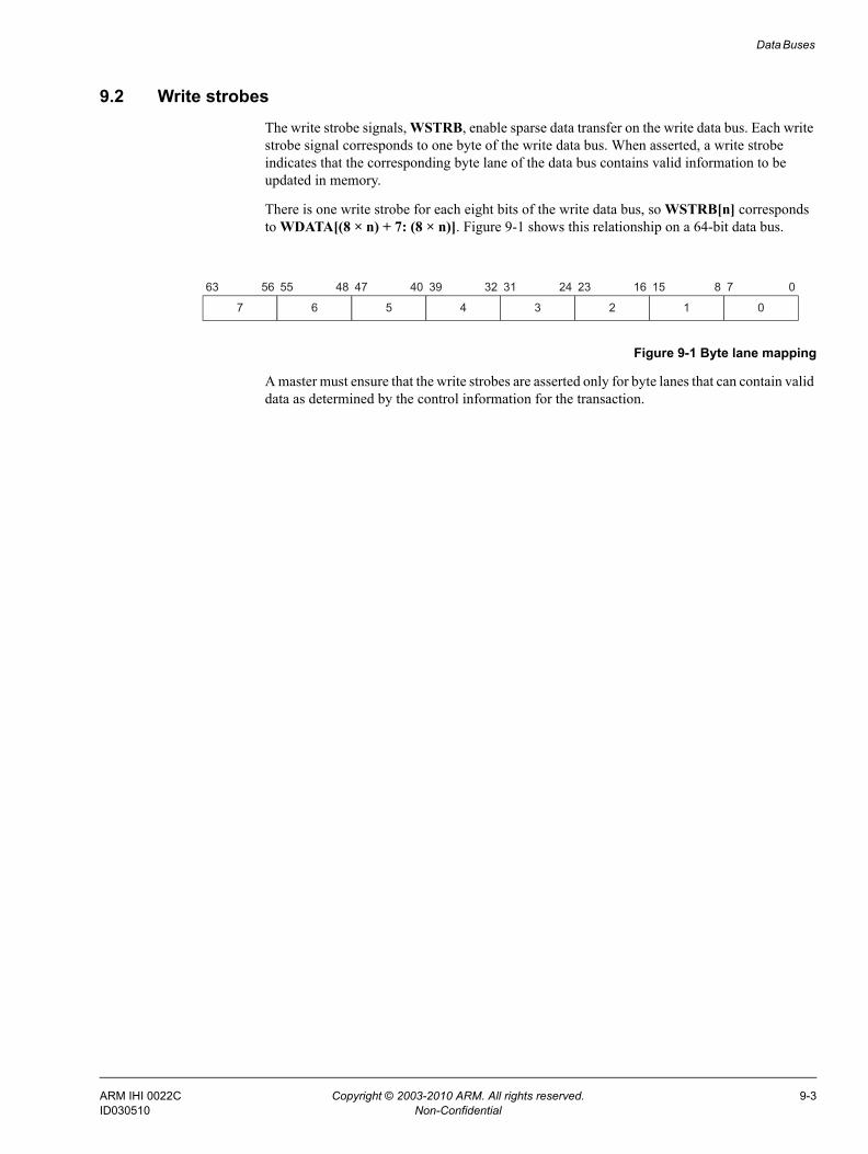
Data Buses
9.2 Write strobesThe write strobe signals, WSTRB, enable sparse data transfer on the write data bus. Each write strobe signal corresponds to one byte of the write data bus. When asserted, a write strobe indicates that the corresponding byte lane of the data bus contains valid information to be updated in memory.
There is one write strobe for each eight bits of the write data bus, so WSTRB[n] corresponds to WDATA[(8 × n) + 7: (8 × n)]. Figure 9-1 shows this relationship on a 64-bit data bus.
Figure 9-1 Byte lane mapping
A master must ensure that the write strobes are asserted only for byte lanes that can contain valid data as determined by the control information for the transaction.
7 6 5 34 2 1 0
63 56 55 48 47 40 39 32 31 24 23 16 15 8 7 0
ARM IHI 0022C Copyright © 2003-2010 ARM. All rights reserved. 9-3ID030510 Non-Confidential
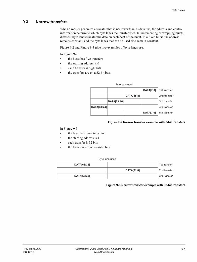
Data Buses
9.3 Narrow transfersWhen a master generates a transfer that is narrower than its data bus, the address and control information determine which byte lanes the transfer uses. In incrementing or wrapping bursts, different byte lanes transfer the data on each beat of the burst. In a fixed burst, the address remains constant, and the byte lanes that can be used also remain constant.
Figure 9-2 and Figure 9-3 give two examples of byte lanes use.
In Figure 9-2:• the burst has five transfers• the starting address is 0• each transfer is eight bits• the transfers are on a 32-bit bus.
Figure 9-2 Narrow transfer example with 8-bit transfers
In Figure 9-3:• the burst has three transfers• the starting address is 4• each transfer is 32 bits• the transfers are on a 64-bit bus.
Figure 9-3 Narrow transfer example with 32-bit transfers
DATA[7:0]
DATA[15:8]
DATA[23:16]
DATA[31:24]
DATA[7:0]
Byte lane used
1st transfer
2nd transfer
3rd transfer
4th transfer
5th transfer
DATA[63:32]
DATA[31:0]
DATA[63:32]
Byte lane used
1st transfer
2nd transfer
3rd transfer
ARM IHI 0022C Copyright © 2003-2010 ARM. All rights reserved. 9-4ID030510 Non-Confidential
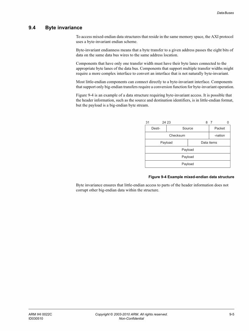
Data Buses
9.4 Byte invarianceTo access mixed-endian data structures that reside in the same memory space, the AXI protocol uses a byte-invariant endian scheme.
Byte-invariant endianness means that a byte transfer to a given address passes the eight bits of data on the same data bus wires to the same address location.
Components that have only one transfer width must have their byte lanes connected to the appropriate byte lanes of the data bus. Components that support multiple transfer widths might require a more complex interface to convert an interface that is not naturally byte-invariant.
Most little-endian components can connect directly to a byte-invariant interface. Components that support only big-endian transfers require a conversion function for byte-invariant operation.
Figure 9-4 is an example of a data structure requiring byte-invariant access. It is possible that the header information, such as the source and destination identifiers, is in little-endian format, but the payload is a big-endian byte stream.
Figure 9-4 Example mixed-endian data structure
Byte invariance ensures that little-endian access to parts of the header information does not corrupt other big-endian data within the structure.
PacketSourceDesti-
-nationChecksum
Data itemsPayload
Payload
Payload
Payload
31 072324 8
ARM IHI 0022C Copyright © 2003-2010 ARM. All rights reserved. 9-5ID030510 Non-Confidential
Chapter 10 Unaligned Transfers
This chapter describes how the AXI protocol handles unaligned transfers. It contains the following sections:• About unaligned transfers on page 10-2• Examples on page 10-3.
ARM IHI 0022C Copyright © 2003-2010 ARM. All rights reserved. 10-1ID030510 Non-Confidential
Unaligned Transfers
10.1 About unaligned transfersThe AXI protocol uses burst-based addressing, which means that each transaction consists of a number of data transfers. Typically, each data transfer is aligned to the size of the transfer. For example, a 32-bit wide transfer is usually aligned to four-byte boundaries. However, there are times when it is desirable to begin a burst at an unaligned address.
For any burst that is made up of data transfers wider than one byte, it is possible that the first bytes that have to be accessed do not align with the natural data width boundary. For example, a 32-bit (four-byte) data packet that starts at a byte address of 0x1002 is not aligned to a 32-bit boundary.
The AXI protocol enables a master to use the low-order address lines to signal an unaligned start address for a burst. The information on the low-order address lines must be consistent with the information contained on the byte lane strobes.
Note The AXI protocol does not require the slave to take special action based on any alignment information from the master.
The master can also simply provide an aligned address and, in a write transaction, rely on the byte lane strobes to provide the information about which byte lanes the data is using.
ARM IHI 0022C Copyright © 2003-2010 ARM. All rights reserved. 10-2ID030510 Non-Confidential
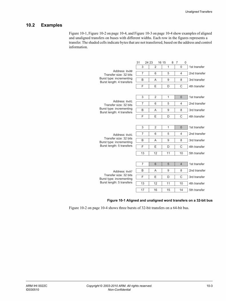
Unaligned Transfers
10.2 ExamplesFigure 10-1, Figure 10-2 on page 10-4, and Figure 10-3 on page 10-4 show examples of aligned and unaligned transfers on buses with different widths. Each row in the figures represents a transfer. The shaded cells indicate bytes that are not transferred, based on the address and control information.
Figure 10-1 Aligned and unaligned word transfers on a 32-bit bus
Figure 10-2 on page 10-4 shows three bursts of 32-bit transfers on a 64-bit bus.
0
0
6 5 4
Address: 0x00Transfer size: 32 bits
Burst type: incrementing
Burst length: 4 transfers
3 2 1 0
7 6 5 4
B A 9 8
F E D C
3 2 1
7 6 5 4
B A 9 8
F E D C
Address: 0x01Transfer size: 32 bits
Burst type: incrementing
Burst length: 4 transfers
3 2 1
7 6 5 4
B A 9 8
F E D C
Address: 0x01Transfer size: 32 bits
Burst type: incrementing
Burst length: 5 transfers
13 12 11 10
7
B A 9 8
F E D C
13 12 11 10
17 16 15 14
Address: 0x07Transfer size: 32 bits
Burst type: incrementing
Burst length: 5 transfers
1st transfer
2nd transfer
3rd transfer
4th transfer
1st transfer
2nd transfer
3rd transfer
4th transfer
1st transfer
2nd transfer
3rd transfer
4th transfer
5th transfer
1st transfer
2nd transfer
3rd transfer
4th transfer
5th transfer
0715 816232431
ARM IHI 0022C Copyright © 2003-2010 ARM. All rights reserved. 10-3ID030510 Non-Confidential
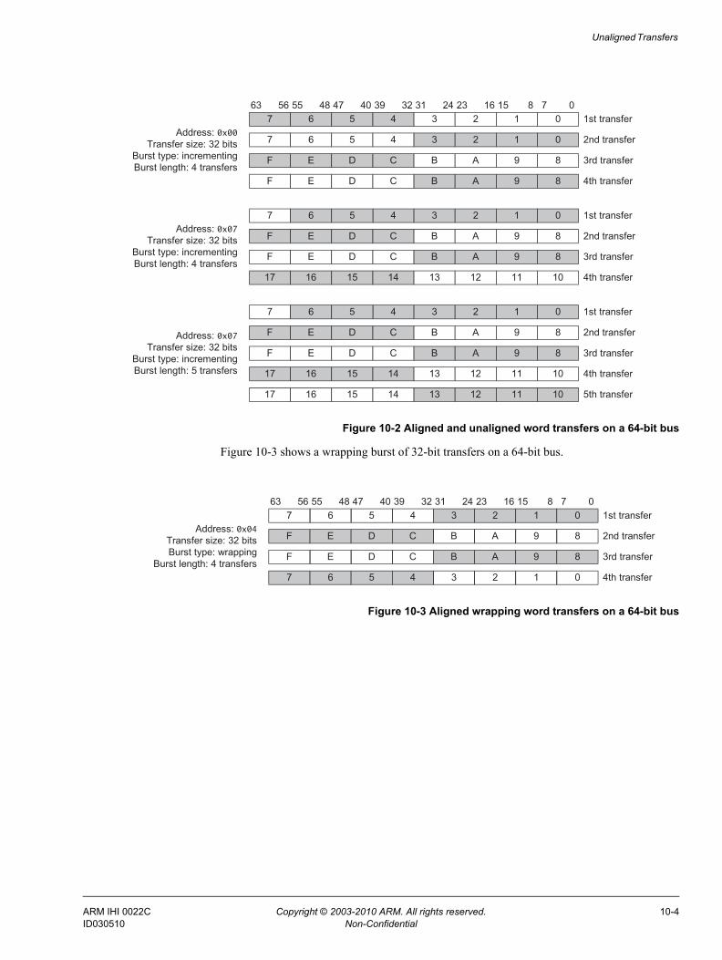
Unaligned Transfers
Figure 10-2 Aligned and unaligned word transfers on a 64-bit bus
Figure 10-3 shows a wrapping burst of 32-bit transfers on a 64-bit bus.
Figure 10-3 Aligned wrapping word transfers on a 64-bit bus
4
4
Address: 0x00Transfer size: 32 bits
Burst type: incrementing
Burst length: 4 transfers
7 6 5 4
7 6 5 4
F E D C
F E D C
7 6 5
F E D C
F E D C
17 16 15 14
Address: 0x07Transfer size: 32 bits
Burst type: incrementing
Burst length: 4 transfers
7 6 5
F E D C
F E D C
17 16 15 14
Address: 0x07Transfer size: 32 bits
Burst type: incrementing
Burst length: 5 transfers
17 16 15 14
3 2 1 0
3 2 1 0
B A 9 8
B A 9 8
03 2 1
B A 9 8
B A 9 8
13 12 11 10
03 2 1
B A 9 8
B A 9 8
13 12 11 10
13 12 11 10
1st transfer
2nd transfer
3rd transfer
4th transfer
5th transfer
1st transfer
2nd transfer
3rd transfer
4th transfer
1st transfer
2nd transfer
3rd transfer
4th transfer
0715 816232431323947 4048555663
Address: 0x04Transfer size: 32 bits
Burst type: wrapping
Burst length: 4 transfers
7 6 5 4
F E D C
F E D C
7 6 5 4
3 2 1 0
B A 9 8
B A 9 8
3 2 1 0
1st transfer
2nd transfer
3rd transfer
4th transfer
0715 816232431323947 4048555663
ARM IHI 0022C Copyright © 2003-2010 ARM. All rights reserved. 10-4ID030510 Non-Confidential
Chapter 11 Clock and Reset
This chapter describes the timing of the AXI clock and reset signals. It contains the following section:• Clock and reset requirements on page 11-2.
ARM IHI 0022C Copyright © 2003-2010 ARM. All rights reserved. 11-1ID030510 Non-Confidential
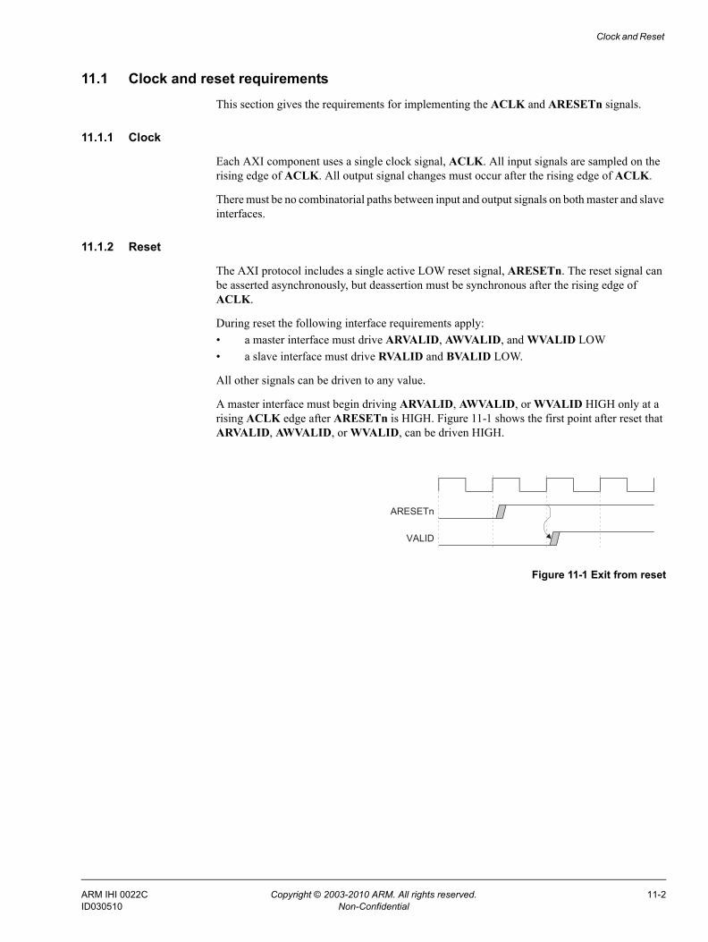
Clock and Reset
11.1 Clock and reset requirementsThis section gives the requirements for implementing the ACLK and ARESETn signals.
11.1.1 Clock
Each AXI component uses a single clock signal, ACLK. All input signals are sampled on the rising edge of ACLK. All output signal changes must occur after the rising edge of ACLK.
There must be no combinatorial paths between input and output signals on both master and slave interfaces.
11.1.2 Reset
The AXI protocol includes a single active LOW reset signal, ARESETn. The reset signal can be asserted asynchronously, but deassertion must be synchronous after the rising edge of ACLK.
During reset the following interface requirements apply:• a master interface must drive ARVALID, AWVALID, and WVALID LOW• a slave interface must drive RVALID and BVALID LOW.
All other signals can be driven to any value.
A master interface must begin driving ARVALID, AWVALID, or WVALID HIGH only at a rising ACLK edge after ARESETn is HIGH. Figure 11-1 shows the first point after reset that ARVALID, AWVALID, or WVALID, can be driven HIGH.
Figure 11-1 Exit from reset
ARESETn
VALID
ARM IHI 0022C Copyright © 2003-2010 ARM. All rights reserved. 11-2ID030510 Non-Confidential
Chapter 12 Low-power Interface
This chapter describes the AXI protocol clock control interface during entry into and exit from a low-power state. It contains the following sections:• About the low-power interface on page 12-2• Low-power clock control on page 12-3.
ARM IHI 0022C Copyright © 2003-2010 ARM. All rights reserved. 12-1ID030510 Non-Confidential
Low-power Interface
12.1 About the low-power interfaceThe low-power interface is an optional extension to the data transfer protocol that targets two different classes of peripherals:
• Peripherals that require a power-down sequence, and that can have their clocks turned off only after they enter a low-power state. These peripherals require an indication from a system clock controller to determine when to initiate the power-down sequence.
• Peripherals that have no power-down sequence, and that can independently indicate when it is acceptable to turn off their clocks.
ARM IHI 0022C Copyright © 2003-2010 ARM. All rights reserved. 12-2ID030510 Non-Confidential
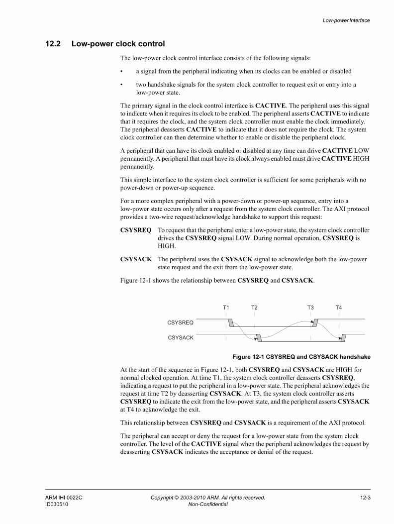
Low-power Interface
12.2 Low-power clock controlThe low-power clock control interface consists of the following signals:
• a signal from the peripheral indicating when its clocks can be enabled or disabled
• two handshake signals for the system clock controller to request exit or entry into a low-power state.
The primary signal in the clock control interface is CACTIVE. The peripheral uses this signal to indicate when it requires its clock to be enabled. The peripheral asserts CACTIVE to indicate that it requires the clock, and the system clock controller must enable the clock immediately. The peripheral deasserts CACTIVE to indicate that it does not require the clock. The system clock controller can then determine whether to enable or disable the peripheral clock.
A peripheral that can have its clock enabled or disabled at any time can drive CACTIVE LOW permanently. A peripheral that must have its clock always enabled must drive CACTIVE HIGH permanently.
This simple interface to the system clock controller is sufficient for some peripherals with no power-down or power-up sequence.
For a more complex peripheral with a power-down or power-up sequence, entry into a low-power state occurs only after a request from the system clock controller. The AXI protocol provides a two-wire request/acknowledge handshake to support this request:
CSYSREQ To request that the peripheral enter a low-power state, the system clock controller drives the CSYSREQ signal LOW. During normal operation, CSYSREQ is HIGH.
CSYSACK The peripheral uses the CSYSACK signal to acknowledge both the low-power state request and the exit from the low-power state.
Figure 12-1 shows the relationship between CSYSREQ and CSYSACK.
Figure 12-1 CSYSREQ and CSYSACK handshake
At the start of the sequence in Figure 12-1, both CSYSREQ and CSYSACK are HIGH for normal clocked operation. At time T1, the system clock controller deasserts CSYSREQ, indicating a request to put the peripheral in a low-power state. The peripheral acknowledges the request at time T2 by deasserting CSYSACK. At T3, the system clock controller asserts CSYSREQ to indicate the exit from the low-power state, and the peripheral asserts CSYSACK at T4 to acknowledge the exit.
This relationship between CSYSREQ and CSYSACK is a requirement of the AXI protocol.
The peripheral can accept or deny the request for a low-power state from the system clock controller. The level of the CACTIVE signal when the peripheral acknowledges the request by deasserting CSYSACK indicates the acceptance or denial of the request.
CSYSREQ
CSYSACK
T1 T2 T3 T4
ARM IHI 0022C Copyright © 2003-2010 ARM. All rights reserved. 12-3ID030510 Non-Confidential
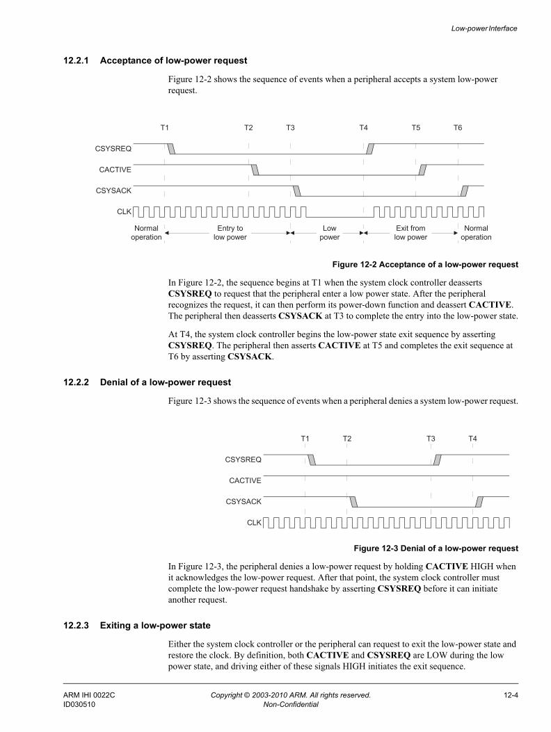
Low-power Interface
12.2.1 Acceptance of low-power request
Figure 12-2 shows the sequence of events when a peripheral accepts a system low-power request.
Figure 12-2 Acceptance of a low-power request
In Figure 12-2, the sequence begins at T1 when the system clock controller deasserts CSYSREQ to request that the peripheral enter a low power state. After the peripheral recognizes the request, it can then perform its power-down function and deassert CACTIVE. The peripheral then deasserts CSYSACK at T3 to complete the entry into the low-power state.
At T4, the system clock controller begins the low-power state exit sequence by asserting CSYSREQ. The peripheral then asserts CACTIVE at T5 and completes the exit sequence at T6 by asserting CSYSACK.
12.2.2 Denial of a low-power request
Figure 12-3 shows the sequence of events when a peripheral denies a system low-power request.
Figure 12-3 Denial of a low-power request
In Figure 12-3, the peripheral denies a low-power request by holding CACTIVE HIGH when it acknowledges the low-power request. After that point, the system clock controller must complete the low-power request handshake by asserting CSYSREQ before it can initiate another request.
12.2.3 Exiting a low-power state
Either the system clock controller or the peripheral can request to exit the low-power state and restore the clock. By definition, both CACTIVE and CSYSREQ are LOW during the low power state, and driving either of these signals HIGH initiates the exit sequence.
Normal
operation
CSYSACK
T1 T2 T3 T4 T5 T6
Normal
operation
CACTIVE
CSYSREQ
Entry to
low power
Low
power
Exit from
low power
CLK
CSYSREQ
T1 T2 T3 T4
CSYSACK
CACTIVE
CLK
ARM IHI 0022C Copyright © 2003-2010 ARM. All rights reserved. 12-4ID030510 Non-Confidential
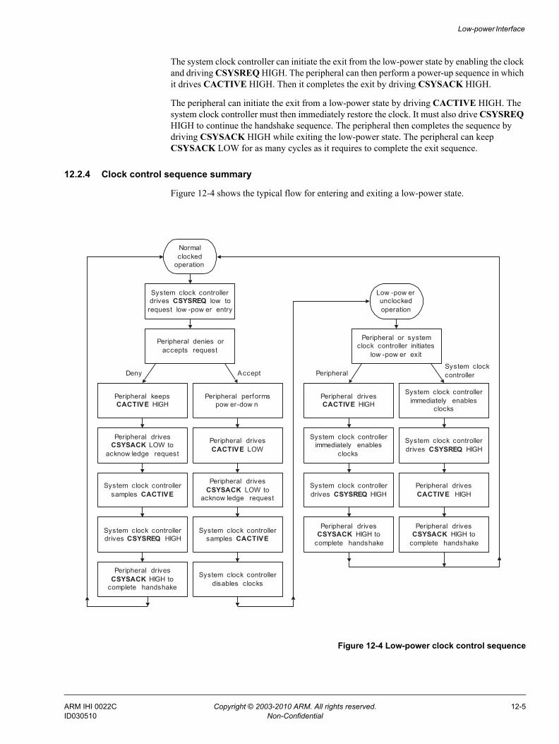
Low-power Interface
The system clock controller can initiate the exit from the low-power state by enabling the clock and driving CSYSREQ HIGH. The peripheral can then perform a power-up sequence in which it drives CACTIVE HIGH. Then it completes the exit by driving CSYSACK HIGH.
The peripheral can initiate the exit from a low-power state by driving CACTIVE HIGH. The system clock controller must then immediately restore the clock. It must also drive CSYSREQ HIGH to continue the handshake sequence. The peripheral then completes the sequence by driving CSYSACK HIGH while exiting the low-power state. The peripheral can keep CSYSACK LOW for as many cycles as it requires to complete the exit sequence.
12.2.4 Clock control sequence summary
Figure 12-4 shows the typical flow for entering and exiting a low-power state.
Figure 12-4 Low-power clock control sequence
Normal
clocked
operation
Low -pow er
unclocked
operation
Peripheral or system
clock controller initiates
low -pow er exit
Peripheral
Peripheral drives
CACTIVE HIGH
System clock controller
immediately enables
clocks
System clock
controller
System clock controller
drives CSYSREQ low to
request low -pow er entry
Peripheral denies or
accepts request
Peripheral keeps
CACTIVE HIGH
Peripheral performs
pow er-dow n
Peripheral drives
CSYSACK LOW to
acknow ledge request
Peripheral drives
CACTIVE LOW
System clock controller
samples CACTIVE
Peripheral drives
CSYSACK LOW to
acknow ledge request
System clock controller
drives CSYSREQ HIGH
System clock controller
samples CACTIVE
System clock controller
disables clocks
Deny Accept
Peripheral drives
CSYSACK HIGH to
complete handshake
Peripheral drives
CSYSACK HIGH to
complete handshake
Peripheral drives
CSYSACK HIGH to
complete handshake
System clock controller
drives CSYSREQ HIGH
Peripheral drives
CACTIVE HIGH
System clock controller
immediately enables
clocks
System clock controller
drives CSYSREQ HIGH
ARM IHI 0022C Copyright © 2003-2010 ARM. All rights reserved. 12-5ID030510 Non-Confidential
Low-power Interface
12.2.5 Combining peripherals in a low-power domain
The system clock controller can combine a number of different peripherals within the same low-power clock domain. Then the clock domain can be treated in the same way as a single peripheral if the following rules are observed:
• The clock domain CACTIVE signal is the logical OR of all the CACTIVE signals within the clock domain. This means that the system clock controller can disable the clocks only when all peripherals indicate that they can be disabled.
• The system clock controller can use a single CSYSREQ signal that is routed to all peripherals within the clock domain.
• The clock domain CSYSACK signal is generated as follows:— the falling edge of CSYSACK occurs when the last falling edge from all of the
peripherals occurs— the rising edge of CSYSACK occurs when the last rising edge from all of the
peripherals occurs.
ARM IHI 0022C Copyright © 2003-2010 ARM. All rights reserved. 12-6ID030510 Non-Confidential
Chapter 13 AXI4
This chapter defines the AXI4 update to the AXI protocol. The AXI Version 1.0 protocol is now referred to as the AXI3 protocol. This chapter is provided for engineers and system designers who are already familiar with implementing systems using the AXI3 protocol and do not require the in depth presentation given in previous chapters. It contains the following sections:• Burst support on page 13-2• Quality of service signaling on page 13-3• Multiple region interfaces on page 13-5• Write response dependencies on page 13-6• AWCACHE and ARCACHE Attributes on page 13-8• Ordering requirements for Non-modifiable transactions on page 13-10• Updated meaning of Read Allocate and Write Allocate on page 13-11• Memory types on page 13-14• Mismatched Attributes on page 13-19• Transaction buffering on page 13-20• Use of device memory types on page 13-21• Legacy considerations on page 13-22• Ordering model on page 13-23• User signals on page 13-28• Locked transactions on page 13-29• Write interleaving on page 13-30• Interoperability and default signals on page 13-31
ARM IHI 0022C Copyright © 2003-2010 ARM. All rights reserved. 13-1ID030510 Non-Confidential
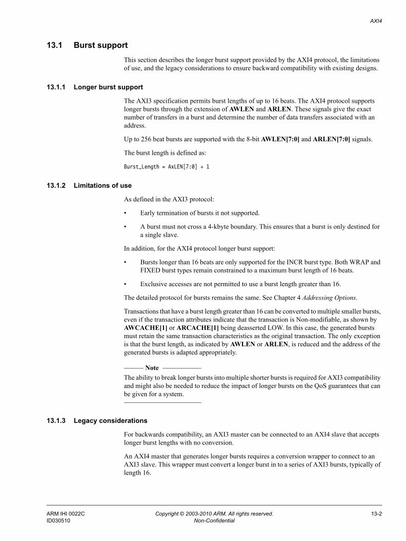
AXI4
13.1 Burst supportThis section describes the longer burst support provided by the AXI4 protocol, the limitations of use, and the legacy considerations to ensure backward compatibility with existing designs.
13.1.1 Longer burst support
The AXI3 specification permits burst lengths of up to 16 beats. The AXI4 protocol supports longer bursts through the extension of AWLEN and ARLEN. These signals give the exact number of transfers in a burst and determine the number of data transfers associated with an address.
Up to 256 beat bursts are supported with the 8-bit AWLEN[7:0] and ARLEN[7:0] signals.
The burst length is defined as:
Burst_Length = AxLEN[7:0] + 1
13.1.2 Limitations of use
As defined in the AXI3 protocol:
• Early termination of bursts it not supported.
• A burst must not cross a 4-kbyte boundary. This ensures that a burst is only destined for a single slave.
In addition, for the AXI4 protocol longer burst support:
• Bursts longer than 16 beats are only supported for the INCR burst type. Both WRAP and FIXED burst types remain constrained to a maximum burst length of 16 beats.
• Exclusive accesses are not permitted to use a burst length greater than 16.
The detailed protocol for bursts remains the same. See Chapter 4 Addressing Options.
Transactions that have a burst length greater than 16 can be converted to multiple smaller bursts, even if the transaction attributes indicate that the transaction is Non-modifiable, as shown by AWCACHE[1] or ARCACHE[1] being deasserted LOW. In this case, the generated bursts must retain the same transaction characteristics as the original transaction. The only exception is that the burst length, as indicated by AWLEN or ARLEN, is reduced and the address of the generated bursts is adapted appropriately.
Note The ability to break longer bursts into multiple shorter bursts is required for AXI3 compatibility and might also be needed to reduce the impact of longer bursts on the QoS guarantees that can be given for a system.
13.1.3 Legacy considerations
For backwards compatibility, an AXI3 master can be connected to an AXI4 slave that accepts longer burst lengths with no conversion.
An AXI4 master that generates longer bursts requires a conversion wrapper to connect to an AXI3 slave. This wrapper must convert a longer burst in to a series of AXI3 bursts, typically of length 16.
ARM IHI 0022C Copyright © 2003-2010 ARM. All rights reserved. 13-2ID030510 Non-Confidential
AXI4
13.2 Quality of service signalingThis section describes the use of additional signaling in the AXI4 protocol to support Quality of Service, QoS.
13.2.1 Additional interface signals
AXI4 interface functionality is extended to support two 4-bit QoS identifiers:
AWQOS 4-bit QoS identifier sent on the write address channel for each write transaction
ARQOS 4-bit QoS identifier sent on the read address channel for each read transaction.
The exact use of the QoS identifier is not specified by the protocol. The preferred use of the AWQOS and ARQOS identifiers is as a priority indicator for the associated write or read transaction. A higher value will indicate a higher priority transaction.
A default value of b0000 indicates that the interface is not actively participating in the QoS scheme.
Note It is acceptable to use additional interpretations of the QoS identifier.
13.2.2 Master considerations
A master can produce its own AWQOS and ARQOS values and if it is capable of producing multiple streams of traffic it can choose different QoS values for the different streams.
Support for QoS in any system requires a system-level understanding of the QoS scheme in use and collaboration between all participating components. For this reason, it is recommended that a master component uses some form of programmable scheme to allow the exact QoS values for any given scenario to be controlled.
If a master component does not support a programmable scheme it can use QoS values that represent the relative priorities of the transactions it generates. These values can then be mapped to alternative system level QoS values if appropriate.
In the case of a master that can not produce its own AWQOS and ARQOS values it must use the default value.
Note It is anticipated that many interconnect implementations will support the concept of a programmable register that allows a QoS value to be assigned to a master and be used instead of the QoS value, either real or default, supplied by the master.
ARM IHI 0022C Copyright © 2003-2010 ARM. All rights reserved. 13-3ID030510 Non-Confidential
AXI4
13.2.3 System considerations
AXI4 defines an interface specification for QoS that can be used with any compatible system- level QoS methodology.
The default system level implementation of QoS is where any component that has the choice of more than one transaction to process will select the transaction with the higher QoS value to process first. This action only occurs when there is no other overriding constraint that requires the transactions to be processed in a particular order.
Note Standard AXI ordering rules take precedence over ordering for QoS purposes.
More sophisticated QoS schemes that are compatible with the scheme described can be implemented.
ARM IHI 0022C Copyright © 2003-2010 ARM. All rights reserved. 13-4ID030510 Non-Confidential
AXI4
13.3 Multiple region interfacesThis section describes the optional support for multiple region interfaces provided by the AXI4 protocol.
13.3.1 Additional interface signals
To support region decode, the AXI4 interface functionality is extended to support two 4-bit region identifiers:
AWREGION region identifier sent on the write address channel for each write transaction
ARREGION region identifier sent on the read address channel for each read transaction.
The 4-bits of region identifier allows up to sixteen different regions to be uniquely identified. The region identifier provides a decode of higher order address bits. The region identifier must remain constant within a 4kbyte address space.
The region identifier allows a single physical interface on a slave to be used for multiple logical interfaces that reside in different locations in the system address map. The use of the region identifier means that the slave does not have to support the address decode between the different logical interfaces.
Typically, AWREGION and ARREGION are produced by an interconnect when performing the address decode function for a single slave that has multiple address decode regions defined in the system address map. If a slave only has a single address decode defined in the system address map, the interconnect must use the default value of AWREGION and ARREGION. See Default signal values on page 13-32.
A number of usage models for the region identifier exist, including but not limited to the following:
• The main data path and control registers of a peripheral can reside at different locations in the address map, and be accessed through a single interface without the need for the slave to perform an address decode.
• A slave can exhibit different behaviors in different memory regions. For example, a slave might have read and write access in one region, but read only access in another region.
A slave is responsible for ensuring that the correct protocol and the correct ordering of transactions is maintained. A slave must ensure that the response to two transactions to different regions with the same AXI ID is provided in the correct order.
A slave is also responsible for ensuring that the correct protocol is followed for any value of AWREGION and ARREGION. If a slave implements less than sixteen regions, then the slave is responsible for ensuring that the correct protocol is followed during access to an un-supported region. How this is achieved is implementation dependant. For example, the slave might ensure this by:
• providing an error response for transactions that access any unsupported region
• aliasing supported regions across unsupported regions to ensure a protocol compliant response is given in all cases.
The AWREGION and ARREGION signals only provide an address decode of the existing address space that can be used by slaves to remove the need for an address decode function. The signals do not create new independent address spaces and the address and region signals must remain consistent. AWREGION and ARREGION must only be present on an interface that is downstream of an address decode function.
ARM IHI 0022C Copyright © 2003-2010 ARM. All rights reserved. 13-5ID030510 Non-Confidential
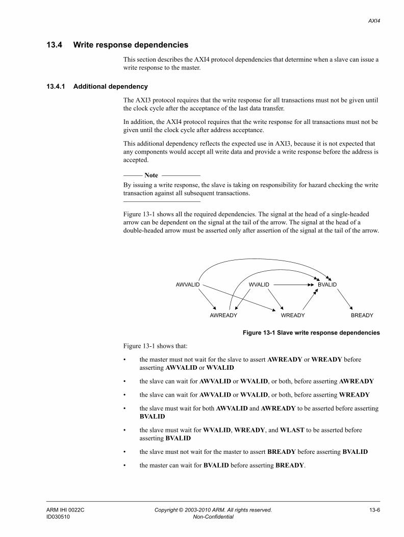
AXI4
13.4 Write response dependenciesThis section describes the AXI4 protocol dependencies that determine when a slave can issue a write response to the master.
13.4.1 Additional dependency
The AXI3 protocol requires that the write response for all transactions must not be given until the clock cycle after the acceptance of the last data transfer.
In addition, the AXI4 protocol requires that the write response for all transactions must not be given until the clock cycle after address acceptance.
This additional dependency reflects the expected use in AXI3, because it is not expected that any components would accept all write data and provide a write response before the address is accepted.
Note By issuing a write response, the slave is taking on responsibility for hazard checking the write transaction against all subsequent transactions.
Figure 13-1 shows all the required dependencies. The signal at the head of a single-headed arrow can be dependent on the signal at the tail of the arrow. The signal at the head of a double-headed arrow must be asserted only after assertion of the signal at the tail of the arrow.
Figure 13-1 Slave write response dependencies
Figure 13-1 shows that:
• the master must not wait for the slave to assert AWREADY or WREADY before asserting AWVALID or WVALID
• the slave can wait for AWVALID or WVALID, or both, before asserting AWREADY
• the slave can wait for AWVALID or WVALID, or both, before asserting WREADY
• the slave must wait for both AWVALID and AWREADY to be asserted before asserting BVALID
• the slave must wait for WVALID, WREADY, and WLAST to be asserted before asserting BVALID
• the slave must not wait for the master to assert BREADY before asserting BVALID
• the master can wait for BVALID before asserting BREADY.
AWREADY
AWVALID WVALID BVALID
BREADYWREADY
ARM IHI 0022C Copyright © 2003-2010 ARM. All rights reserved. 13-6ID030510 Non-Confidential
AXI4
13.4.2 Legacy considerations
The additional new address dependency means that an AXI3 slave that accepts all write data and provides a write response before accepting the address is not compliant with AXI4. Converting an AXI3 legacy slave to AXI4 requires the addition of a wrapper that ensures a returning write response is not provided until the appropriate address has been accepted by the slave.
Note It is recommended that any new AXI3 slave is designed with this additional native dependency.
Any AXI3 master is already compatible with the AXI4 write response requirements.
ARM IHI 0022C Copyright © 2003-2010 ARM. All rights reserved. 13-7ID030510 Non-Confidential
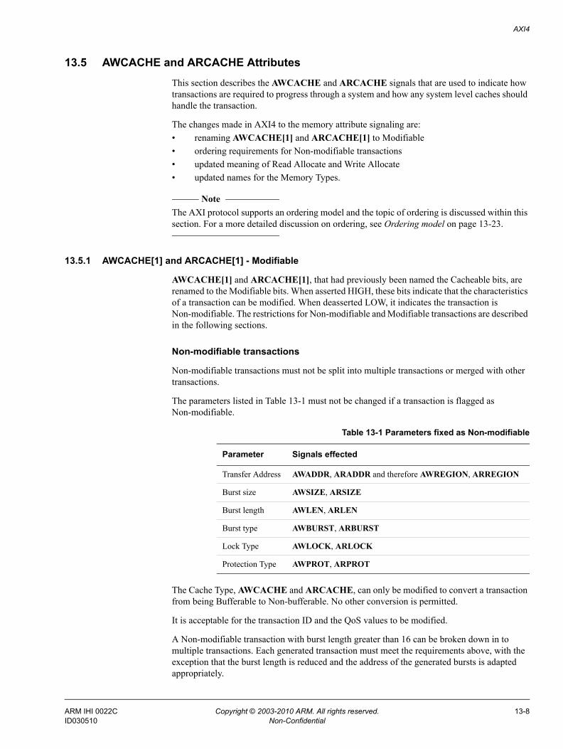
AXI4
13.5 AWCACHE and ARCACHE AttributesThis section describes the AWCACHE and ARCACHE signals that are used to indicate how transactions are required to progress through a system and how any system level caches should handle the transaction.
The changes made in AXI4 to the memory attribute signaling are:• renaming AWCACHE[1] and ARCACHE[1] to Modifiable• ordering requirements for Non-modifiable transactions• updated meaning of Read Allocate and Write Allocate• updated names for the Memory Types.
Note The AXI protocol supports an ordering model and the topic of ordering is discussed within this section. For a more detailed discussion on ordering, see Ordering model on page 13-23.
13.5.1 AWCACHE[1] and ARCACHE[1] - Modifiable
AWCACHE[1] and ARCACHE[1], that had previously been named the Cacheable bits, are renamed to the Modifiable bits. When asserted HIGH, these bits indicate that the characteristics of a transaction can be modified. When deasserted LOW, it indicates the transaction is Non-modifiable. The restrictions for Non-modifiable and Modifiable transactions are described in the following sections.
Non-modifiable transactions
Non-modifiable transactions must not be split into multiple transactions or merged with other transactions.
The parameters listed in Table 13-1 must not be changed if a transaction is flagged as Non-modifiable.
The Cache Type, AWCACHE and ARCACHE, can only be modified to convert a transaction from being Bufferable to Non-bufferable. No other conversion is permitted.
It is acceptable for the transaction ID and the QoS values to be modified.
A Non-modifiable transaction with burst length greater than 16 can be broken down in to multiple transactions. Each generated transaction must meet the requirements above, with the exception that the burst length is reduced and the address of the generated bursts is adapted appropriately.
Table 13-1 Parameters fixed as Non-modifiable
Parameter Signals effected
Transfer Address AWADDR, ARADDR and therefore AWREGION, ARREGION
Burst size AWSIZE, ARSIZE
Burst length AWLEN, ARLEN
Burst type AWBURST, ARBURST
Lock Type AWLOCK, ARLOCK
Protection Type AWPROT, ARPROT
ARM IHI 0022C Copyright © 2003-2010 ARM. All rights reserved. 13-8ID030510 Non-Confidential
AXI4
Note There are circumstances where it is not possible to meet the requirements of Non-modifiable transactions. When downsizing to a bus width narrower than that required by the transaction size, AWSIZE or ARSIZE, the transaction must be modified.
Components that perform such an operation can optionally include a mechanism to indicate that a modification has occurred. This can assist with software debug.
Modifiable transactions
A transaction that is Modifiable can be manipulated in a number of ways:
• a transaction can be broken in to multiple transactions
• multiple transactions can be merged into a single transaction
• a read transaction can fetch more data than required
• a write transaction can access a larger address range than required, making use of strobes to ensure that only the appropriate locations are updated
• the transfer address (AWADDR or ARADDR), the burst size (AWSIZE or ARSIZE), burst length (AWLEN or ARLEN), and burst type (AWBURST or ARBURST) of each generated transaction can be modified.
The following must not be changed:• Lock Type: AWLOCK or ARLOCK• Protection Type: AWPROT or ARPROT.
The Cache Type, AWCACHE or ARCACHE, can be modified, but any modification must ensure that the visibility of transactions by other components is not reduced, either by preventing propagation of transactions to the required point, or by changing the need to look up a transaction in a cache. Any modification to the cache type attributes must be consistent for all transactions to the same address range.
It is acceptable for the transaction ID and the QoS values to be modified.
No transaction modification is allowed that can cause accesses to a different 4kbyte address space than that of the original transaction. Also, no transaction modification is allowed that causes a single access to the same single-copy atomicity sized region to be performed as multiple accesses. See Single-copy atomicity size on page 13-26.
ARM IHI 0022C Copyright © 2003-2010 ARM. All rights reserved. 13-9ID030510 Non-Confidential
AXI4
13.6 Ordering requirements for Non-modifiable transactionsAXI4 requires that ordering is preserved between any Non-modifiable transactions (AWCACHE[1] or ARCACHE[1] is deasserted LOW), using the same AXI ID that are destined for the same slave device. This ensures that the order in which transactions are issued by the master is the same as the order they are received by the slave. The ordering must be preserved, irrespective of the address of the transaction, if the transactions are destined for the same slave.
Ordering between the independent read and write channels can only be guaranteed if a transaction in one direction has been issued after a transaction in the other direction has received a response. If a transaction in one direction is issued before the response in the other direction is received then no ordering exists between the transactions.
No guarantee can be made about the relative ordering of transactions destined for different slaves. Because the address map boundary between different physical slave devices is an implementation defined boundary, if the boundary between slave devices is not known then all Non-modifiable transactions with the same AXI ID on the same path must remain ordered.
This ordering requirement applies between all Non-modifiable transactions, including between Non-bufferable and Bufferable transactions. When a response is given to a transaction from an intermediate point the component giving the response is responsible for ensuring the correct ordering.
For more information on the ordering model see Ordering model on page 13-23
ARM IHI 0022C Copyright © 2003-2010 ARM. All rights reserved. 13-10ID030510 Non-Confidential
AXI4
13.7 Updated meaning of Read Allocate and Write AllocateThe meaning of the Read Allocate and Write Allocate bits is updated so that one bit indicates if an allocation occurs for the transaction and the other bit indicates if an allocation could have been made due to another transaction.
For read transactions, the write allocate bit is redefined to indicate that:
• the location could have been previously allocated in the cache because of a write transaction (as the AXI3 definition)
• the location could have been previously allocated in the cache because of the actions of another master (additional AXI4 definition).
For write transactions, the read allocate bit is redefined to indicate that:
• the location could have been previously allocated in the cache because of a read transaction (as the AXI3 definition)
• the location could have been previously allocated in the cache because of the actions of another master (additional AXI4 definition).
These changes mean:
• a transaction must be looked up in a cache if the value of AWCACHE[3:2] or ARCACHE[3:2] is not b00
• a transaction does not need to be looked up in a cache if the value of AWCACHE[3:2] or ARCACHE[3:2] is b00.
Note The change to the definition of AWCACHE and ARCACHE means that these signals can differ for a read and write transaction to the same location.
ARM IHI 0022C Copyright © 2003-2010 ARM. All rights reserved. 13-11ID030510 Non-Confidential
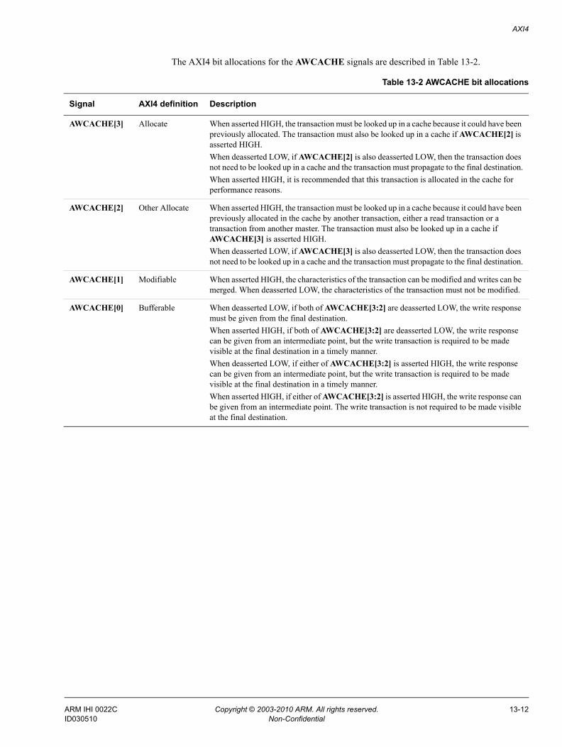
AXI4
The AXI4 bit allocations for the AWCACHE signals are described in Table 13-2.
Table 13-2 AWCACHE bit allocations
Signal AXI4 definition Description
AWCACHE[3] Allocate When asserted HIGH, the transaction must be looked up in a cache because it could have been previously allocated. The transaction must also be looked up in a cache if AWCACHE[2] is asserted HIGH.When deasserted LOW, if AWCACHE[2] is also deasserted LOW, then the transaction does not need to be looked up in a cache and the transaction must propagate to the final destination.When asserted HIGH, it is recommended that this transaction is allocated in the cache for performance reasons.
AWCACHE[2] Other Allocate When asserted HIGH, the transaction must be looked up in a cache because it could have been previously allocated in the cache by another transaction, either a read transaction or a transaction from another master. The transaction must also be looked up in a cache if AWCACHE[3] is asserted HIGH.When deasserted LOW, if AWCACHE[3] is also deasserted LOW, then the transaction does not need to be looked up in a cache and the transaction must propagate to the final destination.
AWCACHE[1] Modifiable When asserted HIGH, the characteristics of the transaction can be modified and writes can be merged. When deasserted LOW, the characteristics of the transaction must not be modified.
AWCACHE[0] Bufferable When deasserted LOW, if both of AWCACHE[3:2] are deasserted LOW, the write response must be given from the final destination.When asserted HIGH, if both of AWCACHE[3:2] are deasserted LOW, the write response can be given from an intermediate point, but the write transaction is required to be made visible at the final destination in a timely manner.When deasserted LOW, if either of AWCACHE[3:2] is asserted HIGH, the write response can be given from an intermediate point, but the write transaction is required to be made visible at the final destination in a timely manner.When asserted HIGH, if either of AWCACHE[3:2] is asserted HIGH, the write response can be given from an intermediate point. The write transaction is not required to be made visible at the final destination.
ARM IHI 0022C Copyright © 2003-2010 ARM. All rights reserved. 13-12ID030510 Non-Confidential
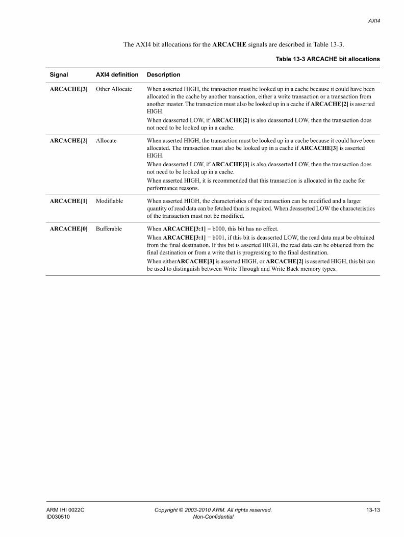
AXI4
The AXI4 bit allocations for the ARCACHE signals are described in Table 13-3.
Table 13-3 ARCACHE bit allocations
Signal AXI4 definition Description
ARCACHE[3] Other Allocate When asserted HIGH, the transaction must be looked up in a cache because it could have been allocated in the cache by another transaction, either a write transaction or a transaction from another master. The transaction must also be looked up in a cache if ARCACHE[2] is asserted HIGH.When deasserted LOW, if ARCACHE[2] is also deasserted LOW, then the transaction does not need to be looked up in a cache.
ARCACHE[2] Allocate When asserted HIGH, the transaction must be looked up in a cache because it could have been allocated. The transaction must also be looked up in a cache if ARCACHE[3] is asserted HIGH.When deasserted LOW, if ARCACHE[3] is also deasserted LOW, then the transaction does not need to be looked up in a cache.When asserted HIGH, it is recommended that this transaction is allocated in the cache for performance reasons.
ARCACHE[1] Modifiable When asserted HIGH, the characteristics of the transaction can be modified and a larger quantity of read data can be fetched than is required. When deasserted LOW the characteristics of the transaction must not be modified.
ARCACHE[0] Bufferable When ARCACHE[3:1] = b000, this bit has no effect.When ARCACHE[3:1] = b001, if this bit is deasserted LOW, the read data must be obtained from the final destination. If this bit is asserted HIGH, the read data can be obtained from the final destination or from a write that is progressing to the final destination.When eitherARCACHE[3] is asserted HIGH, or ARCACHE[2] is asserted HIGH, this bit can be used to distinguish between Write Through and Write Back memory types.
ARM IHI 0022C Copyright © 2003-2010 ARM. All rights reserved. 13-13ID030510 Non-Confidential
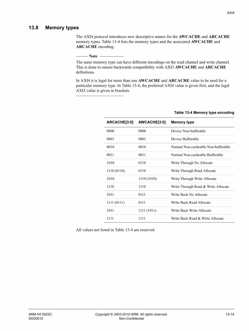
AXI4
13.8 Memory typesThe AXI4 protocol introduces new descriptive names for the AWCACHE and ARCACHE memory types. Table 13-4 lists the memory types and the associated AWCACHE and ARCACHE encoding.
Note The same memory type can have different encodings on the read channel and write channel. This is done to ensure backwards compatibility with AXI3 AWCACHE and ARCACHE definitions.
In AXI4 it is legal for more than one AWCACHE and ARCACHE value to be used for a particular memory type. In Table 13-4, the preferred AXI4 value is given first, and the legal AXI3 value is given in brackets.
All values not listed in Table 13-4 are reserved.
Table 13-4 Memory type encoding
ARCACHE[3:0] AWCACHE[3:0] Memory type
0000 0000 Device Non-bufferable
0001 0001 Device Bufferable
0010 0010 Normal Non-cacheable Non-bufferable
0011 0011 Normal Non-cacheable Bufferable
1010 0110 Write Through No Allocate
1110 (0110) 0110 Write Through Read Allocate
1010 1110 (1010) Write Through Write Allocate
1110 1110 Write Through Read & Write Allocate
1011 0111 Write Back No Allocate
1111 (0111) 0111 Write Back Read Allocate
1011 1111 (1011) Write Back Write Allocate
1111 1111 Write Back Read & Write Allocate
ARM IHI 0022C Copyright © 2003-2010 ARM. All rights reserved. 13-14ID030510 Non-Confidential
AXI4
13.8.1 Memory type requirements
This section describes the required behavior for each of the memory types.
Device Non-bufferable
The required behavior for the Device Non-bufferable memory type is:
• Write response must be obtained from the final destination.
• Read data must be obtained from the final destination.
• Transaction characteristics must not be modified.
• Reads must not be pre-fetched. Writes must not be merged.
• All Non-modifiable read and write transactions (AWCACHE[1] = 0 orARCACHE[1] = 0) from the same ID to the same slave must remain ordered.
Device Bufferable
The required behavior for the Device Bufferable memory type is:
• Write response can be obtained from an intermediate point.
• Write transactions must be made visible at the final destination in a timely manner.
• Read data must be obtained from the final destination.
• Transaction characteristics must not be modified.
• Reads must not be pre-fetched. Writes must not be merged.
• All Non-modifiable read and write transactions (AWCACHE[1] = 0 orARCACHE[1] = 0) from the same ID to the same slave must remain ordered.
Note Both Device memory types are defined to be Non-modifiable. In this protocol specification the terms Device memory and Non-modifiable memory are used interchangeably.
For read transactions there is no difference in the required behavior for Device Non-bufferable and Device Bufferable memory types.
For all Device transactions it is required that transactions to the same slave with the same ID remain ordered, irrespective of the address of the transaction. This ordering requirement applies to all Non-modifiable transactions. Two transactions with the same ID must remain ordered even if one is of memory type Device Non-bufferable and the other is of memory type Device Bufferable.
See Ordering requirements for Non-modifiable transactions on page 13-10.
ARM IHI 0022C Copyright © 2003-2010 ARM. All rights reserved. 13-15ID030510 Non-Confidential
AXI4
Normal Non-cacheable Non-bufferable
The required behavior for the Normal Non-cacheable Non-bufferable memory type is:
• Write response must be obtained from the final destination.
• Read data must be obtained from the final destination.
• Transaction characteristics can be modified.
• Writes can be merged.
• Read and write transactions from the same ID to an overlapping address must remain ordered.
Normal Non-cacheable Bufferable
The required behavior for the Normal Non-cacheable Bufferable memory type is:
• Write response can be obtained from an intermediate point.
• Write transactions must be made visible at the final destination in a timely manner.
• No mechanism is provided to determine when write transactions are visible at the final destination.
• Read data must be obtained either from the final destination or from a write transaction that is progressing to its final destination.If read data is obtained from a write transaction it must be obtained from the most recent version of the write and the data must not be cached to service a later read.
• Transaction characteristics can be modified.
• Writes can be merged.
• Read and write transactions from the same ID to an overlapping address must remain ordered.
Note For a Normal Non-cacheable Bufferable read, it is acceptable for data to be obtained from a write transaction that is still progressing to its final destination. This is indistinguishable from the read and write transactions propagating to the final destination at the same time.
ARM IHI 0022C Copyright © 2003-2010 ARM. All rights reserved. 13-16ID030510 Non-Confidential
AXI4
Write Through No Allocate
The required behavior for the Write Through No Allocate memory type is:
• Write response can be obtained from an intermediate point.
• Write transactions must be made visible at the final destination in a timely manner.
• No mechanism is provided to determine when write transactions are visible at the final destination.
• Read data can be obtained from an intermediate cached copy.
• Transaction characteristics can be modified.
• Reads can be pre-fetched.
• Writes can be merged.
• A cache lookup is required for read and write transactions.
• Read and write transactions from the same ID to an overlapping address must remain ordered.
• Allocation of either read or write transactions is not recommended for performance reasons, but is not prohibited.
Write Through Read Allocate
The required behavior for the Write Through Read Allocate memory type is as for Write Through No Allocate except for the allocation hint that:• allocation of read transactions is recommended for performance reasons• allocation of write transactions is not recommended for performance reasons.
However, allocation is neither required or prohibited for all transactions.
Write Through Write Allocate
The required behavior for the Write Through Write Allocate memory type is as for Write Through No Allocate except for the allocation hint that:• allocation of read transactions is not recommended for performance reasons.• allocation of write transactions is recommended for performance reasons
However, allocation is neither required or prohibited for all transactions.
Write Through Read and Write Allocate
The required behavior for the Write Through Read and Write Allocate memory type is as for Write Through No Allocate except for the allocation hint that: • allocation of read transactions is recommended for performance reasons• allocation of write transactions is recommended for performance reasons.
However, allocation is not required.
ARM IHI 0022C Copyright © 2003-2010 ARM. All rights reserved. 13-17ID030510 Non-Confidential
AXI4
Write Back No Allocate
The required behavior for the Write Back No Allocate memory type is:
• Write response can be obtained from an intermediate point.
• Write transactions are not required to be made visible at the final destination.
• Read data can be obtained from an intermediate cached copy.
• Transaction characteristics can be modified.
• Reads can be pre-fetched.
• Writes can be merged.
• A cache lookup is required for read and write transactions.
• Read and write transactions from the same ID to an overlapping address must remain ordered.
• Allocation of either read or write transactions is not recommended for performance reasons, but is not prohibited.
Write Back Read Allocate
The required behavior for the Write Back Read Allocate memory type is as for Write Back No Allocate except for the allocation hint that:• allocation of read transactions is recommended for performance reasons• allocation of write transactions is not recommended for performance reasons.
However, allocation is neither required or prohibited for all transactions.
Write Back Write Allocate
The required behavior for the Write Back Write Allocate memory type is as for Write Back No Allocate except for the allocation hint that:• allocation of read transactions is not recommended for performance reasons.• allocation of write transactions is recommended for performance reasons
However, allocation is neither required or prohibited for all transactions.
Write Back Read and Write Allocate
The required behavior for the Write Back Read and Write Allocate memory type is as for Write Back No Allocate except for the allocation hint that: • allocation of read transactions is recommended for performance reasons• allocation of write transactions is recommended for performance reasons.
However, allocation is not required.
ARM IHI 0022C Copyright © 2003-2010 ARM. All rights reserved. 13-18ID030510 Non-Confidential
AXI4
13.9 Mismatched AttributesIt is acceptable for multiple agents that are both accessing the same area of memory to use mismatched memory attributes. However, for functional correctness the following rules must be obeyed:
• All masters accessing the same area of memory must agree on whether or not that area of memory can be cached at a given level of hierarchy. The rules to be applied are:Address region not cacheable
All masters must use transactions with both ARCACHE[3:2] LOW or both AWCACHE[3:2] LOW.
Address region cacheable All masters must use transactions with either of ARCACHE[3:2] HIGH or either of AWCACHE[3:2] HIGH.
• Allocation hints can differ between masters.
• If an address region is memory type Normal Non-cacheable, it is acceptable for any master to access it using a transaction that is memory type Device.
• If an address region is defined as being a bufferable memory type, it is acceptable for any master to access it using transactions that do not permit bufferable behavior, that is, transactions that require the response from the final destination.
13.9.1 Changing memory attributes
It is acceptable to change the attributes used for a particular memory region from one type to another incompatible type. For example, the attribute can be changed from Write Through Cacheable to Normal Non-cacheable, with the use of a suitable process to perform the change. Typically, this will involve a process where all masters stop accessing the region, a single agent then performs any required cache maintenance operations, then all masters can recommence accessing the memory region with the new attributes.
ARM IHI 0022C Copyright © 2003-2010 ARM. All rights reserved. 13-19ID030510 Non-Confidential
AXI4
13.10 Transaction bufferingCertain memory types do not require that transaction responses come from the final destination, but they do require that the transactions are made visible at the final destination in a timely manner. The memory types that exhibit this behavior are: Device Bufferable, Normal Non-cacheable Bufferable, and Write Through.
All three memory types require that write transactions are made visible at the final destination in a timely manner, but the behavior for reads is different:
• for Device Bufferable memory, read data must be obtained from the final destination
• for Normal Non-cacheable Bufferable memory, read data must be obtained either from the final destination or from a write transaction that is progressing to its final destination
• for Write Through memory, read data can be obtained from an intermediate cached copy.
The protocol does not give an absolute time during which a transaction must become visible at the final destination. It is only required that in a sufficiently idle system the transaction makes progress towards the final destination without requiring any explicit action.
For Normal Non-cacheable Bufferable memory, any intermediate buffer that is capable of providing a response to a transaction, while ensuring that the transaction is made visible to the final destination in a timely manner, must also over time ensure that read transactions propagate downstream of the buffer. This means that in the case of forwarding to a read transaction, the forwarding must not be allowed to occur indefinitely. In a similar manner to the way that writes drain out of the buffer over time, any data used for forwarding must not be allowed to persist indefinitely. The exact mechanism used to determine how long data used for forwarding can persist is not defined. However, it is important that such a mechanism does not allow the act of reading the data to reset the time period. Continued polling of the same location by a master would prevent the timeout of a held value and thus prevent visibility of an updated downstream value.
Any intermediate buffer that is capable of holding and merging write transactions must also ensure that transactions do not remain within the buffer indefinitely. For example, the act of merging write transactions should not reset the mechanism to determine when a write is drained. Otherwise continued writing of a location could prevent the timeout of a held write and prevent visibility of a write downstream.
ARM IHI 0022C Copyright © 2003-2010 ARM. All rights reserved. 13-20ID030510 Non-Confidential
AXI4
13.11 Use of device memory typesThe specification allows the combined use of memory types Device Non-buffered and Device Buffered to force transactions to reach their final destination.
A transaction that is marked as Device Buffered is required to reach its final destination in a timely manner, but there is no indication back to the issuing master when the transaction is visible to all other masters.
If a Device Buffered transaction or stream of transactions is followed by a Device Non-buffered transaction that uses the same AXI ID, it will force all of the Device Buffered transactions to reach the final destination before a response is given to the Device Non-buffered transaction.
A Device Non-buffered transaction can only guarantee the completion of Device Buffered transactions that are issued with the same ID, that are to the same slave device. The minimum address space occupied by a single slave device is 4kbytes.
ARM IHI 0022C Copyright © 2003-2010 ARM. All rights reserved. 13-21ID030510 Non-Confidential
AXI4
13.12 Legacy considerationsAXI4 provides additional clarification on the expected use of the AWCACHE and ARCACHE memory attributes.
In particular, AXI4 adds an additional requirement that all Device type transactions using the same ID to the same slave are ordered with respect to each other. This is not an explicit requirement of AXI3. Any AXI4 component that relies on this behavior can not be connected to an AXI3 interconnect that does not exhibit this behavior.
In the majority of existing system designs it is expected that the AXI3 interconnect will implement the requirements specified for AWCACHE and ARCACHE in AXI4.
It is recommended that any new AXI3 designs follow the AXI4 recommendations.
For AWCACHE and ARCACHE bits names and memory type names it is required that AXI4 only uses the new terms. AXI3 components can use either the AXI3 or AXI4 names.
ARM IHI 0022C Copyright © 2003-2010 ARM. All rights reserved. 13-22ID030510 Non-Confidential
AXI4
13.13 Ordering modelThis section describes the ordering model supported by the AXI4 Protocol.
13.13.1 Definition of Ordering model
The AXI protocol supports an ordering model based on the use of the AXI ID transaction identifier.
The principles are that for transactions with the same ID:
• transactions to a peripheral device, as indicated by the Device memory type, must arrive at the peripheral in the same order that they are issued, irrespective of the address of the transactions
• transactions to a memory that are to the same, or overlapping, addresses must arrive at the memory in the same order that they are issued.
The AXI ordering model also requires that all transactions with the same ID in the same direction must provide their responses in order.
In order to support the use of independent read and write address channels, it is required that if an ordering relationship is required between two transactions with the same ID, that are in different directions, then a response to the earlier transaction must be received before the later transaction is issued.
If a transaction is issued in one direction before an earlier transaction in the opposite direction has been given a response then there are no ordering guarantees between them.
13.13.2 Master ordering
A master that issues multiple transactions in the same direction (read or write) with the same ID has the following guarantees about the ordering of these transactions:
• The order of response at the master to all transactions must be the same as the order of issue.
• For Device Memory, the order of arrival at the slave must be the same as the order of issue.
• For Normal Memory, the order of arrival of transactions to the same or overlapping address, must be the same as the order of issue.
Note Transactions to the same or overlapping address, is defined as being when two
transactions access bytes within the same single-copy atomic address range. See Single-copy atomicity size on page 13-26.
If a master requires ordering between read and write transactions, it must ensure that a response is received for the previous transaction before issuing the next transaction.
ARM IHI 0022C Copyright © 2003-2010 ARM. All rights reserved. 13-23ID030510 Non-Confidential

AXI4
Interconnect ordering
To meet the requirements of the ordering model, the interconnect must ensure that:
• The order of transactions in the same direction with the same ID to a Device is preserved.
• The order of transactions in the same direction with the same ID to overlapping addresses is preserved.
• The order of write responses with the same ID is preserved.
• The order of read data responses with the same ID is preserved.
• Any manipulation of the AXI ID values associated with a transaction must ensure that the preceeding itemized guarantees remain.
• Any component that gives a response to a transaction before it reaches its final destination must ensure the preceeding itemized guarantees are maintained downstream. See Response before final destination on page 13-25.
Slave ordering
For slaves the following must be ensured:
• Any write transaction that has been given a response must be observed by any subsequent write or read transaction, independent of the transaction ID.
• Any write transaction to Device memory must be observed by any subsequent write to Device memory with the same ID, even if a response has not yet been given.
• Any write transaction to Normal memory must be observed by any subsequent write to an overlapping address with the same ID, even if a response has not yet been given.
• The response to multiple write transactions with the same ID must be given in the same order that the transactions arrived.
• The response to multiple write transactions with different IDs can be given in any order.
• Any read transaction that has been given a response must be observed by any subsequent write or read transaction, independent of the transaction ID.
• Any read transaction to Device memory must be observed by any subsequent read to Device memory with the same ID, even if a response has not yet been given.
• The response to multiple read transactions with the same ID must be given in the same order that the transactions arrive.
• The response to multiple read transactions with different IDs can be given in any order.
ARM IHI 0022C Copyright © 2003-2010 ARM. All rights reserved. 13-24ID030510 Non-Confidential
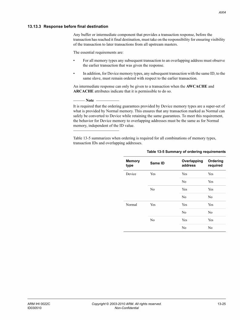
AXI4
13.13.3 Response before final destination
Any buffer or intermediate component that provides a transaction response, before the transaction has reached it final destination, must take on the responsibility for ensuring visibility of the transaction to later transactions from all upstream masters.
The essential requirements are:
• For all memory types any subsequent transaction to an overlapping address must observe the earlier transaction that was given the response.
• In addition, for Device memory types, any subsequent transaction with the same ID, to the same slave, must remain ordered with respect to the earlier transaction.
An intermediate response can only be given to a transaction when the AWCACHE and ARCACHE attributes indicate that it is permissible to do so.
Note It is required that the ordering guarantees provided by Device memory types are a super-set of what is provided by Normal memory. This ensures that any transaction marked as Normal can safely be converted to Device while retaining the same guarantees. To meet this requirement, the behavior for Device memory to overlapping addresses must be the same as for Normal memory, independent of the ID value.
Table 13-5 summarizes when ordering is required for all combinations of memory types, transaction IDs and overlapping addresses.
Table 13-5 Summary of ordering requirements
Memorytype Same ID Overlapping
addressOrderingrequired
Device Yes Yes Yes
No Yes
No Yes Yes
No No
Normal Yes Yes Yes
No No
No Yes Yes
No No
ARM IHI 0022C Copyright © 2003-2010 ARM. All rights reserved. 13-25ID030510 Non-Confidential
AXI4
13.13.4 Single-copy atomicity size
The term single-copy atomicity size defines the minimum number of bytes that are updated in an atomic fashion by a transaction. A transaction that is larger than the single-copy atomicity size must update memory in blocks of at least the single-copy atomicity size. The exact instant that the data is updated is not important, what must be ensured is that no master can ever observe a partially updated form of the data. For example, in many systems certain data structures, such as linked lists, are made up of 32-bit atomic elements. This requires that the entire 32-bit value must be updated at the same time. It is not acceptable for another master to observe a partial update of 16-bits, at one point in time, and then the other 16-bits, at a later point in time.
With more complex systems, there is a requirement to use larger atomic elements, in particular 64-bit atomic elements. This allows masters to communicate using data structures that are based upon these larger atomic elements.
The size of the atomic elements that are supported in a system is important because all of the components involved in a given communication must support the required size of atomic element. If two masters are communicating through an interconnect and a single slave, then all of the components involved must ensure that transactions of the required size are treated atomically.
The AXI4 protocol does not require a specific single-copy atomicity size and systems can be designed to implement different single-copy atomicity sizes. It is also allowable for different groups of components to have different single-copy atomicity sizes for communication between themselves.
In AXI4 the term single-copy atomic group is used to describe the groups of components in a system that can communicate at the required atomicity. For example, Figure 13-2 on page 13-27 shows a system in which the processor, DSP, interconnect, and off-chip DRAM are all in a group of components that can guarantee 64-bit single-copy atomic communication, while the DMA controller, peripherals, and on-chip SRAM memory are in a 32-bit single-copy atomic group.
ARM IHI 0022C Copyright © 2003-2010 ARM. All rights reserved. 13-26ID030510 Non-Confidential
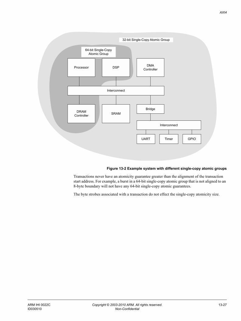
AXI4
Figure 13-2 Example system with different single-copy atomic groups
Transactions never have an atomicity guarantee greater than the alignment of the transaction start address. For example, a burst in a 64-bit single-copy atomic group that is not aligned to an 8-byte boundary will not have any 64-bit single-copy atomic guarantees.
The byte strobes associated with a transaction do not effect the single-copy atomicity size.
Processor
Interconnect
DSP DMAController
DRAMController SRAM
Bridge
Interconnect
UART Timer GPIO
64-bit Single-CopyAtomic Group
32-bit Single-Copy Atomic Group
ARM IHI 0022C Copyright © 2003-2010 ARM. All rights reserved. 13-27ID030510 Non-Confidential
AXI4
13.14 User signalsThis section defines a set of User signals that can accompany each AXI4 channel.
Generally, the use of User signals is not recommended because their functionality is not defined in the AXI4 protocol and this can lead to interoperability issues if two components use the same User signals in an incompatible manner.
13.14.1 Signal naming
The User signal names defined for each AXI4 channel are:
AWUSER Write address channel User signals.
ARUSER Read address channel User signals.
WUSER Write data channel User signals.
RUSER Read data channel User signals.
BUSER Write response channel User signals.
13.14.2 Usage considerations
Where User signals are implemented it is not required that User signals are supported on all channels.
It is not expected that User signals are supported at generic master and slave component interfaces.
It is recommended that interconnect components include support for User signals to allow them to be passed between master and slave components.The width of User signals is implementation defined and can be different for each of the channels.
ARM IHI 0022C Copyright © 2003-2010 ARM. All rights reserved. 13-28ID030510 Non-Confidential
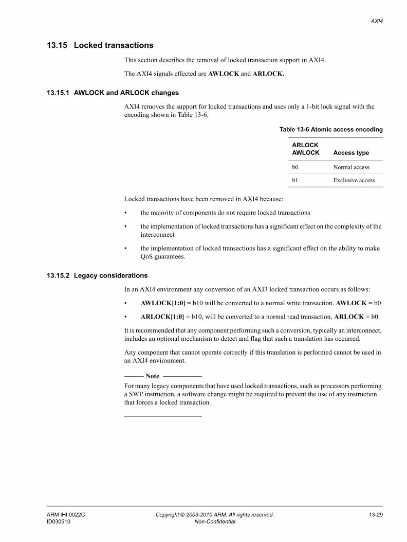
AXI4
13.15 Locked transactionsThis section describes the removal of locked transaction support in AXI4.
The AXI4 signals effected are AWLOCK and ARLOCK.
13.15.1 AWLOCK and ARLOCK changes
AXI4 removes the support for locked transactions and uses only a 1-bit lock signal with the encoding shown in Table 13-6.
Locked transactions have been removed in AXI4 because:
• the majority of components do not require locked transactions
• the implementation of locked transactions has a significant effect on the complexity of the interconnect
• the implementation of locked transactions has a significant effect on the ability to make QoS guarantees.
13.15.2 Legacy considerations
In an AXI4 environment any conversion of an AXI3 locked transaction occurs as follows:
• AWLOCK[1:0] = b10 will be converted to a normal write transaction, AWLOCK = b0
• ARLOCK[1:0] = b10, will be converted to a normal read transaction, ARLOCK = b0.
It is recommended that any component performing such a conversion, typically an interconnect, includes an optional mechanism to detect and flag that such a translation has occurred.
Any component that cannot operate correctly if this translation is performed cannot be used in an AXI4 environment.
Note For many legacy components that have used locked transactions, such as processors performing a SWP instruction, a software change might be required to prevent the use of any instruction that forces a locked transaction.
Table 13-6 Atomic access encoding
ARLOCKAWLOCK Access type
b0 Normal access
b1 Exclusive access
ARM IHI 0022C Copyright © 2003-2010 ARM. All rights reserved. 13-29ID030510 Non-Confidential
AXI4
13.16 Write interleavingThis section describes the removal of write interleaving support in AXI4.
In AXI4, all write data for a transaction must be provided in consecutive transfers on the write data channel.
The AXI4 signals effected are WID.
13.16.1 Removal of WID
The removal of write interleaving makes the information conveyed on the WID signals redundant. All write data must be in the same order as the associated write addresses. Any component that requires the depreciated WID information can obtain this from the write address channel signals AWID.
In AXI4, the WID signals are removed to reduce the pin-count of the interface.
13.16.2 Legacy considerations
The majority of AXI3 masters do not support write interleaving and will not require updating to meet the AXI4 requirement for no write interleaving.
Any AXI3 master that does support write interleaving must already support a method for configuring the write interleaving depth to be set to a value of 1, in order to support operation with any slave that has a write interleaving depth of 1. Any such AXI3 master must have its write interleaving depth configured to a value of 1 to be compatible with AXI4.
Any AXI3 slave can accept non-interleaved write data and therefore there are no legacy considerations for an AXI3 slave.
Note WID signals can be generated from AWID for an AXI3 slave that requires WID information.
ARM IHI 0022C Copyright © 2003-2010 ARM. All rights reserved. 13-30ID030510 Non-Confidential
AXI4
13.17 Interoperability and default signalsThis section describes the interoperability of the AXI4 interface.
Not every component is required to use the full set of signals available on an AXI4 interface. To simplify the connection of components that do not use every signal, major categories of interfaces are defined together with the restrictions that apply to each category.
13.17.1 Interoperability principles
In general, components must support all combinations of inputs, but do not have to generate all combinations of outputs. For example, a slave must support all the different possible lengths of burst, but a master only has to generate the types of burst that it uses. This policy ensures that all components will work with all other components.
The conditions under which a signal can be omitted from the interface are:
• An output signal can be omitted if the operation of the master or slave always drives the output signal to the same as default value. See Default signal values on page 13-32.
• An input signal can be omitted if the master or slave does not need to observe the input signal for correct functional operation.
Note Interconnect components can also omit signals when appropriate. For example, when a signal is only being driven by default values, it is not required that the default value is transported across the interconnect. It can be created at its destination. Similarly, if a signal is not used at any destination then it is not required to be transported across the interconnect.
13.17.2 Major interface categories
The major interface categories are described in the following sections.
Read write interface
A read write interface includes the five AXI4 channels used for data transfer:AR Read address channel.R Read data channel.AW Write address channel.W Write data channel.B Write response channel.
Read only interface
A read only interface supports only read transactions and includes the two AXI4 read channels:AR Read address channel.R Read data channel.
Note A read only interface does not support exclusive accesses.
ARM IHI 0022C Copyright © 2003-2010 ARM. All rights reserved. 13-31ID030510 Non-Confidential
AXI4
Write only interface
A write only interface supports only write transactions and includes the three AXI4 write channels:AW Write address channel.W Write data channel.B Write response channel.
Note A write only interface does not support exclusive accesses.
13.17.3 Memory slaves and peripheral slaves
Slaves can be classified as Memory Slaves or Peripheral Slaves.
Memory slaves are required to handle all transaction types correctly.
Peripheral Slaves are expected to have a defined method of access that is typically described in the components datasheet. Any accesses outside of that defined as allowable might cause the peripheral slave to fail. Any access that is outside of the allowable behavior is expected to complete in a protocol-correct manner, to prevent system deadlock, but continued correct operation of the peripheral slave is not required.
Because peripheral slaves are required to only work correctly for defined access methods, it is possible for a peripheral slave to have a significantly reduced set of interface signals.
13.17.4 Default signal values
It is generally suggested that, for maximum IP reuse, all signals are included in a component interface. This is because the presence of the signal reduces the risk of error at the system integration phase of the design flow and it can also aid with some design flows that do not effectively support default values for absent signals.
Table 13-7 on page 13-33 lists the required and optional write channel signals for masters and memory slaves, and the default signal values required when an optional signal is not present.
Table 13-8 on page 13-34 lists the required and optional read channel signals for masters and memory slaves, and the default signal values required when an optional signal is not present.
For additional information on the default signal value requirements see the following sections:• Master addresses on page 13-35• Slave addresses on page 13-35• Memory slaves on page 13-35• Write transactions on page 13-35• Read transactions on page 13-35• Response signaling on page 13-36• Non-secure and secure accesses on page 13-36
Optional signals are defined as:
Optional Outputs If the value required by the component does not match the default value in Table 13-7 on page 13-33, then the component is required to have the output signal present.
ARM IHI 0022C Copyright © 2003-2010 ARM. All rights reserved. 13-32ID030510 Non-Confidential
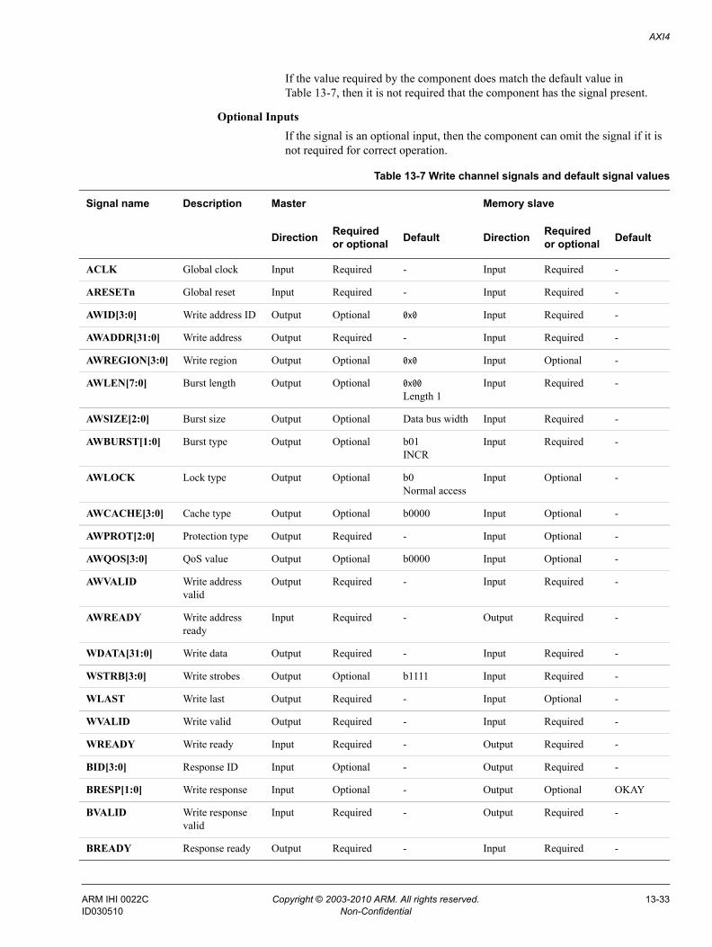
AXI4
If the value required by the component does match the default value in Table 13-7, then it is not required that the component has the signal present.
Optional Inputs If the signal is an optional input, then the component can omit the signal if it is not required for correct operation.
Table 13-7 Write channel signals and default signal values
Signal name Description Master Memory slave
Direction Requiredor optional Default Direction Required
or optional Default
ACLK Global clock Input Required - Input Required -
ARESETn Global reset Input Required - Input Required -
AWID[3:0] Write address ID Output Optional 0x0 Input Required -
AWADDR[31:0] Write address Output Required - Input Required -
AWREGION[3:0] Write region Output Optional 0x0 Input Optional -
AWLEN[7:0] Burst length Output Optional 0x00
Length 1Input Required -
AWSIZE[2:0] Burst size Output Optional Data bus width Input Required -
AWBURST[1:0] Burst type Output Optional b01INCR
Input Required -
AWLOCK Lock type Output Optional b0Normal access
Input Optional -
AWCACHE[3:0] Cache type Output Optional b0000 Input Optional -
AWPROT[2:0] Protection type Output Required - Input Optional -
AWQOS[3:0] QoS value Output Optional b0000 Input Optional -
AWVALID Write addressvalid
Output Required - Input Required -
AWREADY Write addressready
Input Required - Output Required -
WDATA[31:0] Write data Output Required - Input Required -
WSTRB[3:0] Write strobes Output Optional b1111 Input Required -
WLAST Write last Output Required - Input Optional -
WVALID Write valid Output Required - Input Required -
WREADY Write ready Input Required - Output Required -
BID[3:0] Response ID Input Optional - Output Required -
BRESP[1:0] Write response Input Optional - Output Optional OKAY
BVALID Write responsevalid
Input Required - Output Required -
BREADY Response ready Output Required - Input Required -
ARM IHI 0022C Copyright © 2003-2010 ARM. All rights reserved. 13-33ID030510 Non-Confidential
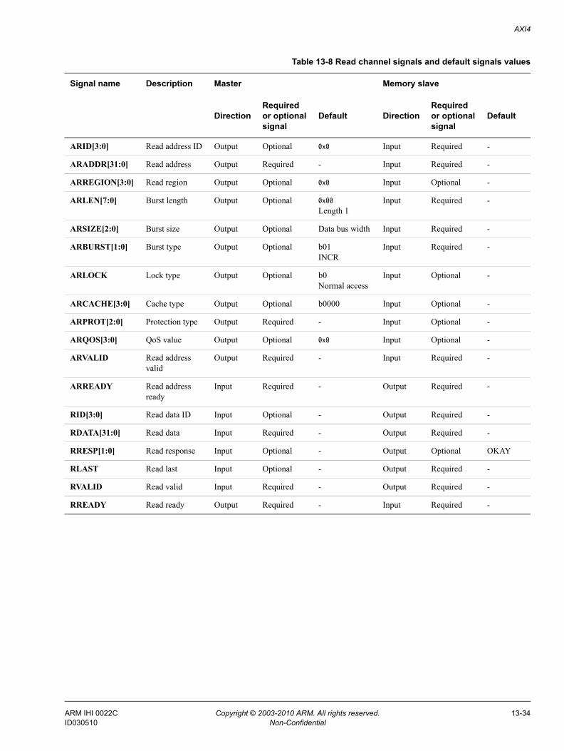
AXI4
Table 13-8 Read channel signals and default signals values
Signal name Description Master Memory slave
DirectionRequiredor optionalsignal
Default DirectionRequiredor optionalsignal
Default
ARID[3:0] Read address ID Output Optional 0x0 Input Required -
ARADDR[31:0] Read address Output Required - Input Required -
ARREGION[3:0] Read region Output Optional 0x0 Input Optional -
ARLEN[7:0] Burst length Output Optional 0x00
Length 1Input Required -
ARSIZE[2:0] Burst size Output Optional Data bus width Input Required -
ARBURST[1:0] Burst type Output Optional b01INCR
Input Required -
ARLOCK Lock type Output Optional b0Normal access
Input Optional -
ARCACHE[3:0] Cache type Output Optional b0000 Input Optional -
ARPROT[2:0] Protection type Output Required - Input Optional -
ARQOS[3:0] QoS value Output Optional 0x0 Input Optional -
ARVALID Read addressvalid
Output Required - Input Required -
ARREADY Read addressready
Input Required - Output Required -
RID[3:0] Read data ID Input Optional - Output Required -
RDATA[31:0] Read data Input Required - Output Required -
RRESP[1:0] Read response Input Optional - Output Optional OKAY
RLAST Read last Input Optional - Output Required -
RVALID Read valid Input Required - Output Required -
RREADY Read ready Output Required - Input Required -
ARM IHI 0022C Copyright © 2003-2010 ARM. All rights reserved. 13-34ID030510 Non-Confidential
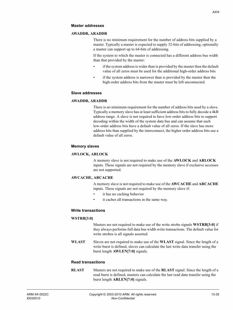
AXI4
Master addresses
AWADDR, ARADDR There is no minimum requirement for the number of address bits supplied by a master. Typically a master is expected to supply 32-bits of addressing, optionally a master can support up to 64-bits of addressing.If the system to which the master is connected has a different address bus width than that provided by the master:• if the system address is wider than is provided by the master then the default
value of all zeros must be used for the additional high-order address bits• if the system address is narrower than is provided by the master then the
high-order address bits from the master must be left unconnected.
Slave addresses
AWADDR, ARADDR There is no minimum requirement for the number of address bits used by a slave. Typically a memory slave has at least sufficient address bits to fully decode a 4kB address range. A slave is not required to have low-order address bits to support decoding within the width of the system data bus and can assume that such low-order address bits have a default value of all zeros. If the slave has more address bits than supplied by the interconnect, the higher order address bits use a default value of all zeros.
Memory slaves
AWLOCK, ARLOCK A memory slave is not required to make use of the AWLOCK and ARLOCK inputs. These signals are not required by the memory slave if exclusive accesses are not supported.
AWCACHE, ARCACHE A memory slave is not required to make use of the AWCACHE and ARCACHE inputs. These signals are not required by the memory slave if:• it has no caching behavior• it caches all transactions in the same way.
Write transactions
WSTRB[3:0] Masters are not required to make use of the write strobe signals WSTRB[3:0] if they always performs full data bus width write transactions. The default value for write strobes is all signals asserted.
WLAST Slaves are not required to make use of the WLAST signal. Since the length of a write burst is defined, slaves can calculate the last write data transfer using the burst length AWLEN[7:0] signals.
Read transactions
RLAST Masters are not required to make use of the RLAST signal. Since the length of a read burst is defined, masters can calculate the last read data transfer using the burst length ARLEN[7:0] signals.
ARM IHI 0022C Copyright © 2003-2010 ARM. All rights reserved. 13-35ID030510 Non-Confidential
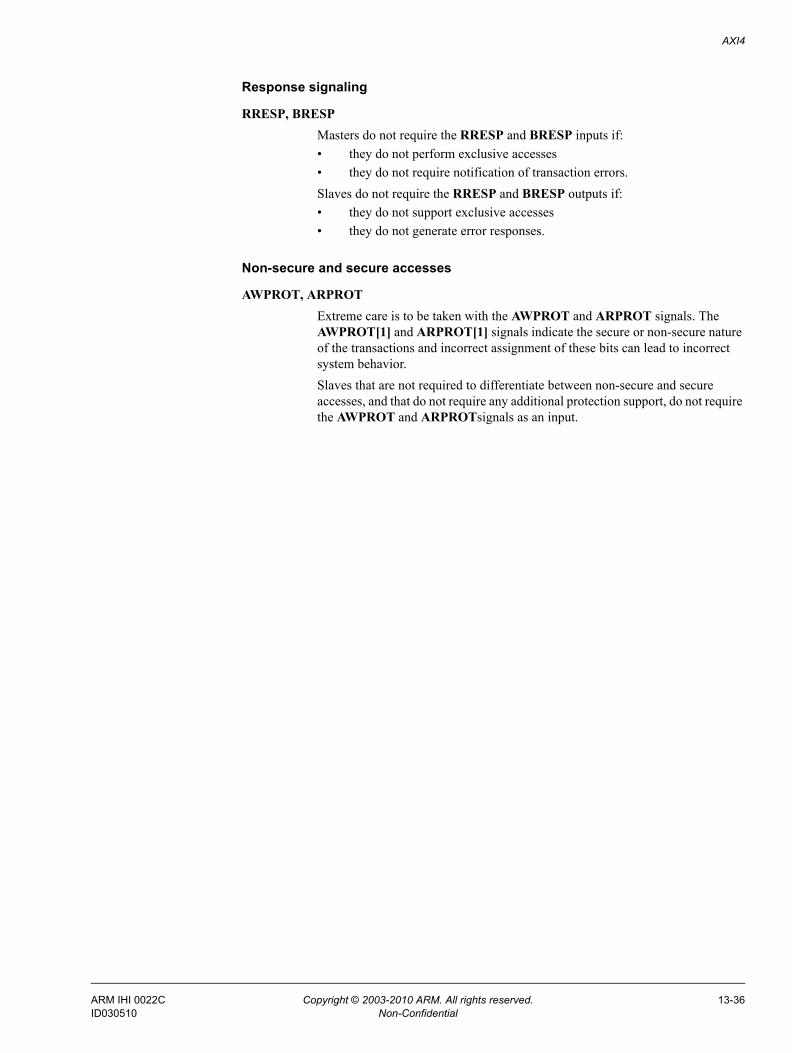
AXI4
Response signaling
RRESP, BRESP Masters do not require the RRESP and BRESP inputs if:• they do not perform exclusive accesses• they do not require notification of transaction errors.Slaves do not require the RRESP and BRESP outputs if:• they do not support exclusive accesses• they do not generate error responses.
Non-secure and secure accesses
AWPROT, ARPROT Extreme care is to be taken with the AWPROT and ARPROT signals. The AWPROT[1] and ARPROT[1] signals indicate the secure or non-secure nature of the transactions and incorrect assignment of these bits can lead to incorrect system behavior.Slaves that are not required to differentiate between non-secure and secure accesses, and that do not require any additional protection support, do not require the AWPROT and ARPROTsignals as an input.
ARM IHI 0022C Copyright © 2003-2010 ARM. All rights reserved. 13-36ID030510 Non-Confidential
Chapter 14 AXI4-Lite
This chapter defines the AXI4-Lite interface. It is provided for engineers and system designers who are designing simpler control register-style interfaces that do not require the full functionality of AXI4. It contains the following sections:• Introduction on page 14-2• Definition of AXI4-Lite on page 14-3• Interoperability on page 14-6• Defined conversion mechanism on page 14-7.• Conversion, Protection, and Detection on page 14-9
ARM IHI 0022C Copyright © 2003-2010 ARM. All rights reserved. 14-1ID030510 Non-Confidential
AXI4-Lite
14.1 IntroductionThe AXI4-Lite interface is a subset of the AXI4 interface intended for communication with control registers in components.
The aim of AXI4-Lite is to allow simple component interfaces to be built that are smaller and also require less design and validation effort.
Having a defined subset of the full AXI4 interface allows many different components to be built using the same subset and also allows a single common conversion component to be used to move between AXI4 and AXI4-Lite interfaces.
The following sections describes the requirements of the AXI4-Lite interface.
ARM IHI 0022C Copyright © 2003-2010 ARM. All rights reserved. 14-2ID030510 Non-Confidential
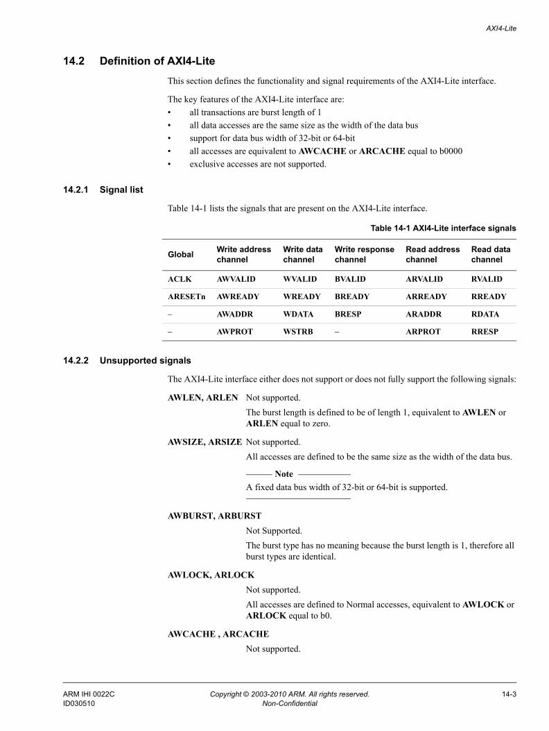
AXI4-Lite
14.2 Definition of AXI4-LiteThis section defines the functionality and signal requirements of the AXI4-Lite interface.
The key features of the AXI4-Lite interface are:• all transactions are burst length of 1• all data accesses are the same size as the width of the data bus• support for data bus width of 32-bit or 64-bit• all accesses are equivalent to AWCACHE or ARCACHE equal to b0000• exclusive accesses are not supported.
14.2.1 Signal list
Table 14-1 lists the signals that are present on the AXI4-Lite interface.
14.2.2 Unsupported signals
The AXI4-Lite interface either does not support or does not fully support the following signals:
AWLEN, ARLEN Not supported.The burst length is defined to be of length 1, equivalent to AWLEN or ARLEN equal to zero.
AWSIZE, ARSIZE Not supported.All accesses are defined to be the same size as the width of the data bus.
Note A fixed data bus width of 32-bit or 64-bit is supported.
AWBURST, ARBURST Not Supported.The burst type has no meaning because the burst length is 1, therefore all burst types are identical.
AWLOCK, ARLOCK Not supported.All accesses are defined to Normal accesses, equivalent to AWLOCK or ARLOCK equal to b0.
AWCACHE , ARCACHE Not supported.
Table 14-1 AXI4-Lite interface signals
Global Write addresschannel
Write datachannel
Write responsechannel
Read addresschannel
Read datachannel
ACLK AWVALID WVALID BVALID ARVALID RVALID
ARESETn AWREADY WREADY BREADY ARREADY RREADY
− AWADDR WDATA BRESP ARADDR RDATA
− AWPROT WSTRB − ARPROT RRESP
ARM IHI 0022C Copyright © 2003-2010 ARM. All rights reserved. 14-3ID030510 Non-Confidential
AXI4-Lite
All accesses are defined to be equivalent to AWCACHE or ARCACHE equal to b0000.
WLAST, RLAST Not supported.All bursts are defined to be of length 1, equivalent to WLAST and RLAST always being asserted.
RRESP, BRESP Not fully supported.The EXOKAY response is not supported on the RRESP and BRESP response channels.
14.2.3 Optional Signals
Multiple outstanding transactions are supported, but a slave design is allowed to restrict this by the appropriate manipulation of the handshake signals.
AXI IDs are not supported. This defines that all transactions must be in order and all accesses must use a single fixed ID value.
Slaves can optionally support AXI ID signals to allow the slave to be used on a full AXI interface without modification. See Interoperability on page 14-6.
Data interleaving is not supported because the burst length is defined to be 1.
14.2.4 Bus width
AXI4-Lite has a fixed data bus width and all transactions are the same width as the data bus. Two options for data bus width are supported, either 32-bit or 64-bit.
It is anticipated that:• the majority of components use a 32-bit interface• only components requiring 64-bit atomic accesses are likely to use a 64-bit interface.
It is acceptable for a 64-bit component to be designed so that it can be accessed by 32-bit masters, but all the transactions to the component must be viewed as 64-bit transactions.
Note This interoperability can be achieved by including, in the register map of the component, locations that are suitable for access by a 32-bit master. Such locations would typically only use the lower 32-bits of the data bus.
ARM IHI 0022C Copyright © 2003-2010 ARM. All rights reserved. 14-4ID030510 Non-Confidential
AXI4-Lite
14.2.5 Write strobes
Writes strobes are supported on the interface. This allows multi-sized registers to be implemented and also allows memory structures to be implemented that can be written using byte and half word accesses.
All master interfaces and interconnect must provide correct write strobes.
Any slave component can choose whether to make use of the write strobes. The options permitted are:• to make full use of the write strobes• to ignore the write strobes and treat all write accesses as being the full data bus width• to detect write strobe combinations that are not supported and provide an error response.
Any slave component that is providing memory-like behavior must fully support write strobes.
If conversion is being used from full AXI to AXI4-Lite, it is acceptable for a write transaction to be generated on AXI4-Lite with all write strobes deasserted. Automatic suppression of such transactions is permitted but not required. See Conversion, Protection, and Detection on page 14-9.
ARM IHI 0022C Copyright © 2003-2010 ARM. All rights reserved. 14-5ID030510 Non-Confidential
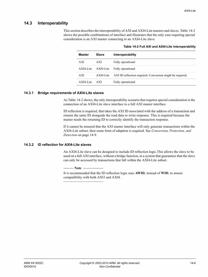
AXI4-Lite
14.3 InteroperabilityThis section describes the interoperability of AXI and AXI4-Lite masters and slaves. Table 14-2 shows the possible combinations of interface and illustrates that the only case requiring special consideration is an AXI master connecting to an AXI4-Lite slave.
14.3.1 Bridge requirements of AXI4-Lite slaves
As Table 14-2 shows, the only interoperability scenario that requires special consideration is the connection of an AXI4-Lite slave interface to a full AXI master interface.
ID reflection is required, that takes the AXI ID associated with the address of a transaction and returns the same ID alongside the read data or write response. This is required because the master needs the returning ID to correctly identify the transaction response.
If it cannot be ensured that the AXI master interface will only generate transactions within the AXI4-Lite subset, then some form of adaption is required. See Conversion, Protection, and Detection on page 14-9.
14.3.2 ID reflection for AXI4-Lite slaves
An AXI4-Lite slave can be designed to include ID reflection logic.This allows the slave to be used on a full AXI interface, without a bridge function, in a system that guarantees that the slave can only be accessed by transactions that fall within the AXI4-Lite subset.
Note It is recommended that the ID reflection logic uses AWID, instead of WID, to ensure compatibility with both AXI3 and AXI4.
Table 14-2 Full AXI and AXI4-Lite interoperability
Master Slave Interoperability
AXI AXI Fully operational
AXI4-Lite AXI4-Lite Fully operational
AXI AXI4-Lite AXI ID reflection required. Conversion might be required.
AXI4-Lite AXI Fully operational
ARM IHI 0022C Copyright © 2003-2010 ARM. All rights reserved. 14-6ID030510 Non-Confidential
AXI4-Lite
14.4 Defined conversion mechanismThis section describes the process required to convert any legal AXI transaction for use on AXI4-Lite. See Conversion, Protection, and Detection on page 14-9 for a more detailed discussion on the advantages and disadvantages of the various approaches that might be used.
14.4.1 Conversion rules
It is assumed that the AXI data width will be equal to or greater than the AXI4-Lite data width. If this is not the case then the AXI data width must first be converted to the AXI4-Lite data width.
The rules for conversion from a full AXI interface are as follows:
• If a transaction has a burst length greater than 1 then the burst is broken into multiple transactions of burst length 1. The number of transactions that are created will depend on the burst length of the original transaction.
• The conversion of bursts with a length greater than 1 must take into consideration the burst type when generating the address for subsequent beats of the burst. An unaligned start address must be incremented and aligned for subsequent beats of an INCR or WRAP burst. For a FIXED burst the same address can be used for all beats.
• Where a write burst with length greater than 1 is converted into multiple write bursts the response for each of the generated transactions must be combined together to produce a single response for the original burst. Any error response is considered sticky, that is, if an error response is received for any of the generated transactions it is retained and the single combined response indicates an error. If both a SLVERR and a DECERR are received then the first response received is the one that is used for the combined response. EXOKAY responses are not permitted on AXI4-Lite, so this option does not need to be considered.
• A transaction that is wider than the AXI4-Lite interface it is destined for is broken into multiple transactions of the same width as the AXI4-Lite interface. For transactions with an unaligned start address, the breaking up of the burst occurs on AXI4-Lite interface width aligned boundaries.
• Where a wide transaction is converted to multiple narrower transactions a combined response must be used for the original transaction. Any error response is considered sticky. If both a SLVERR and a DECERR are received then the first response received is used for the combined response. EXOKAY responses are not permitted on AXI4-Lite, so this option does not need to be considered.
• Transactions that are narrower than the AXI4-Lite interface are passed directly and are not converted.
• Write strobes are passed directly and are not converted.
• Write transactions with no strobes can be passed directly and are not required to be suppressed.
• The AWLOCK and ARLOCK signals are discarded for all transactions. For a sequence of locked transactions the guaranteed nature of the locking is lost. However, it is only when there is a downstream arbitration point that the locked nature of the transactions is lost. For an exclusive sequence, the fail-safe signaling of AXI is such that the exclusive write must always fail.
ARM IHI 0022C Copyright © 2003-2010 ARM. All rights reserved. 14-7ID030510 Non-Confidential

AXI4-Lite
• The AWCACHE and ARCACHE signals are discarded. All transactions are treated as Non-modifiable and Non-bufferable. This is acceptable as it is functionally correct to treat Modifiable accesses as Non-modifiable and Bufferable accesses as Non-bufferable.
• The AWPROT and ARPROT signals are passed directly and are not converted.
• The WLAST and RLAST signals are discarded.
ARM IHI 0022C Copyright © 2003-2010 ARM. All rights reserved. 14-8ID030510 Non-Confidential
AXI4-Lite
14.5 Conversion, Protection, and DetectionConnection of an AXI4-Lite slave to an AXI4 master requires some form of adaption if it can not be ensured that the master will only issue transactions within the AXI4-Lite subset.
This section describes three techniques that can be adopted in a system design to aid with the interoperability of components and the debugging of system design problems. These techniques are:
Conversion This requires the conversion of all transactions to a format that is compatible with the AXI4-Lite subset.
Protection This requires the detection of a non-compliant transaction, followed by the suppression of the transaction and the return of an error response to the master that generated the transaction.
Detection This requires observing any transaction that falls outside of the AXI4-Lite subset and notifying the software of the unexpected access, while still allowing the access to proceed.
14.5.1 Conversion and protection levels
There are several different levels of conversion and protection that can be implemented:
Full conversion This converts all forms of AXI transaction, as described in Defined conversion mechanism on page 14-7.
Simple conversion with protection This propagates transactions that only require a simple conversion, like the discarding of AWLOCK and ARLOCK or AWCACHE and ARCACHE, but suppresses and error reports transactions that require a more complex task, like burst length or data width conversion.
Full protection Suppress and generate an error for every transaction that does not fall within the AXI4-Lite subset.
14.5.2 Implementation considerations
A protection mechanism that suppresses transactions must provide a protocol-compliant error response to prevent deadlock. For example, read burst transactions require an error for each beat of the burst and a correctly asserted RLAST signal.
Detection used alongside conversion allows hardware to be designed that does not prevent unexpected accesses from occurring, but does provide a mechanism for notifying the software of the unexpected access, thus speeding up the debug process.
In complex designs the advantage of the conversion plus detection approach is that it allows unforeseen future usage models to be supported. For example, at design time it might be considered that only the processor programs the control register of a peripheral, but in practice, the peripheral might need to be programmed by other devices, like a DSP or a DMA controller, that is not able to generate exactly the required AXI4-Lite access.
ARM IHI 0022C Copyright © 2003-2010 ARM. All rights reserved. 14-9ID030510 Non-Confidential
AXI4-Lite
The advantages and disadvantages of the different approaches are summarized as:
• Protection requires a lower gate count.
• Conversion ensures the interface can operate with unforeseen accesses.
• Conversion increases the portability of software from one system to another.
• Conversion might allow more efficient use of the AXI infrastructure. For example, a burst of writes to a FIFO can be issued as a single burst, rather than needing to be issued as a set of single transactions.
• Conversion might allow more efficient use of narrow links, where the address and data payload signals are shared.
• Conversion provides more flexibility in component types that can be placed on the AXI4-Lite interface. By converting bursts and allowing sparse strobes it is possible to place memory on AXI4-Lite, with no burst conversion required in the memory device. This is essentially a sharing of the burst conversion logic.
ARM IHI 0022C Copyright © 2003-2010 ARM. All rights reserved. 14-10ID030510 Non-Confidential
ARM IHI 0022C Copyright © 2003-2010 ARM. All rights reserved. A-1ID030510 Non-Confidential
Appendix A Revisions
This appendix describes the technical changes between released issues of this book.
Table A-1 Issue B
Change Location Affects
First release of Version 1.0 - -
Table A-2 Differences between issue B and issue C
Change Location Affects
Additional section describing the chapter layout of Version 2.0 of the document
AXI revisions on page 1-2 All revisions
Additional details on the constraints for the VALID and READY handshake
Handshake process on page 3-2 All revisions
Additional equation for wrapping bursts Burst address on page 4-7 All revisions
Additional chapter describing the AXI4 update to the AXI3 protocol
Chapter 13 AXI4 All revisions
Additional chapter describing the AXI4-Lite subset of the AXI4 protocol
Chapter 14 AXI4-Lite All revisions
Appendix added describing changes made between issues of the document
Appendix A Revisions All revisions


![AXI Protocol Checker v1 - Xilinx · The AXI Protocol Checker core monitors AXI interfaces. When attached to an interface, it ... See ARM AMBA® AXI Protocol v2.0 [Ref 1]. Performance](https://img.pdfslide.net/doc/110x75/5b158bc17f8b9ac7128d1298/axi-protocol-checker-v1-xilinx-the-axi-protocol-checker-core-monitors-axi.jpg)


![LogiCORE IP AXI to APB Bridge v2 - XilinxThe 32-bit AXI4-Lite interface on the AXI to APB Bridge core is based on the AMBA AXI and ACE Protocol Specification v2.0 [Ref 1]. The core](https://img.pdfslide.net/doc/110x75/5ea76a1bf3eb741af75f6d89/logicore-ip-axi-to-apb-bridge-v2-xilinx-the-32-bit-axi4-lite-interface-on-the.jpg)