Embed Size (px)
Citation preview
VOUTP
VOUTN
VDD2
GND2GND1
VINN
VINP
VDD1
AMC1100
HV+
HV-
To Load
FloatingPower Supply
3.3 V, or 5.0 V
RSHUNT
Gate Driver
Gate Driver
5.0 V
ADS7263
Product
Folder
Sample &Buy
Technical
Documents
Tools &
Software
Support &Community
ReferenceDesign
AMC1100SBAS562A –APRIL 2012–REVISED DECEMBER 2014
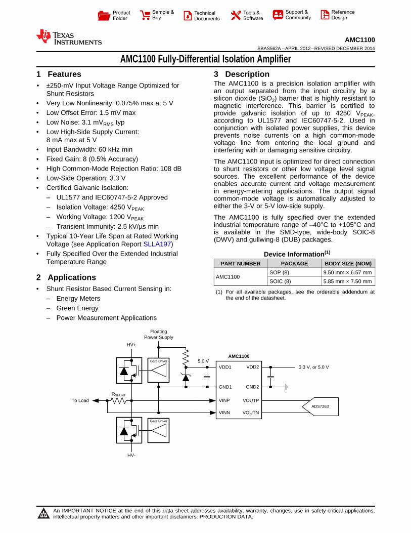
AMC1100 Fully-Differential Isolation Amplifier1 Features 3 Description
The AMC1100 is a precision isolation amplifier with1• ±250-mV Input Voltage Range Optimized for
an output separated from the input circuitry by aShunt Resistorssilicon dioxide (SiO2) barrier that is highly resistant to
• Very Low Nonlinearity: 0.075% max at 5 V magnetic interference. This barrier is certified to• Low Offset Error: 1.5 mV max provide galvanic isolation of up to 4250 VPEAK,
according to UL1577 and IEC60747-5-2. Used in• Low Noise: 3.1 mVRMS typconjunction with isolated power supplies, this device• Low High-Side Supply Current: prevents noise currents on a high common-mode
8 mA max at 5 V voltage line from entering the local ground and• Input Bandwidth: 60 kHz min interfering with or damaging sensitive circuitry.• Fixed Gain: 8 (0.5% Accuracy) The AMC1100 input is optimized for direct connection• High Common-Mode Rejection Ratio: 108 dB to shunt resistors or other low voltage level signal
sources. The excellent performance of the device• Low-Side Operation: 3.3 Venables accurate current and voltage measurement• Certified Galvanic Isolation: in energy-metering applications. The output signal
– UL1577 and IEC60747-5-2 Approved common-mode voltage is automatically adjusted toeither the 3-V or 5-V low-side supply.– Isolation Voltage: 4250 VPEAK
– Working Voltage: 1200 VPEAK The AMC1100 is fully specified over the extendedindustrial temperature range of –40°C to +105°C and– Transient Immunity: 2.5 kV/µs minis available in the SMD-type, wide-body SOIC-8• Typical 10-Year Life Span at Rated Working (DWV) and gullwing-8 (DUB) packages.
Voltage (see Application Report SLLA197)• Fully Specified Over the Extended Industrial Device Information(1)
Temperature Range PART NUMBER PACKAGE BODY SIZE (NOM)SOP (8) 9.50 mm × 6.57 mm
AMC11002 Applications SOIC (8) 5.85 mm × 7.50 mm• Shunt Resistor Based Current Sensing in: (1) For all available packages, see the orderable addendum at
the end of the datasheet.– Energy Meters– Green Energy– Power Measurement Applications
1
An IMPORTANT NOTICE at the end of this data sheet addresses availability, warranty, changes, use in safety-critical applications,intellectual property matters and other important disclaimers. PRODUCTION DATA.
AMC1100SBAS562A –APRIL 2012–REVISED DECEMBER 2014 www.ti.com
Table of Contents7.1 Overview ................................................................. 121 Features .................................................................. 17.2 Functional Block Diagram ....................................... 122 Applications ........................................................... 17.3 Feature Description................................................. 133 Description ............................................................. 17.4 Device Functional Modes........................................ 144 Revision History..................................................... 2
8 Application and Implementation ........................ 155 Pin Configuration and Functions ......................... 38.1 Application Information............................................ 156 Specifications......................................................... 38.2 Typical Applications ................................................ 156.1 Absolute Maximum Ratings ...................................... 3
9 Power Supply Recommendations ...................... 196.2 ESD Ratings.............................................................. 310 Layout................................................................... 206.3 Recommended Operating Conditions....................... 4
10.1 Layout Guidelines ................................................. 206.4 Thermal Information .................................................. 410.2 Layout Example .................................................... 206.5 Regulatory Information.............................................. 4
11 Device and Documentation Support ................. 216.6 IEC 60747-5-2 Insulation Characteristics ................. 411.1 Device Support...................................................... 216.7 IEC Safety Limiting Values ....................................... 511.2 Documentation Support ........................................ 236.8 IEC 61000-4-5 Ratings ............................................. 511.3 Trademarks ........................................................... 236.9 IEC 60664-1 Ratings................................................. 511.4 Electrostatic Discharge Caution............................ 236.10 Package Characteristics ........................................ 511.5 Glossary ................................................................ 236.11 Electrical Characteristics......................................... 6
12 Mechanical, Packaging, and Orderable6.12 Typical Characteristics ............................................ 7Information ........................................................... 237 Detailed Description ............................................ 12
4 Revision History
Changes from Original (April 2012) to Revision A Page
• Changed format to meet latest data sheet standards ............................................................................................................ 1• Added ESD Rating table and Feature Description, Device Functional Modes, Application and
Implementation, Power Supply Recommendations, Layout, Device and Documentation Support, and Mechanical,Packaging, and Orderable Information sections..................................................................................................................... 1
• Added DWV package to document ........................................................................................................................................ 1• Deleted Package and Ordering Information section............................................................................................................... 3
2 Submit Documentation Feedback Copyright © 2012–2014, Texas Instruments Incorporated
Product Folder Links: AMC1100
1
2
3
4
8
7
6
5
VDD2
VOUTP
VOUTN
GND2
VDD1
VINP
VINN
GND1
AMC1100www.ti.com SBAS562A –APRIL 2012–REVISED DECEMBER 2014
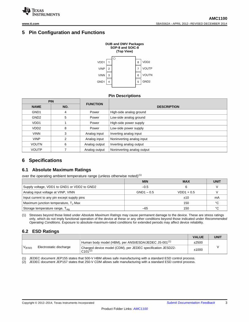
5 Pin Configuration and Functions
DUB and DWV PackagesSOP-8 and SOIC-8
(Top View)
Pin DescriptionsPIN
FUNCTIONNAME NO. DESCRIPTIONGND1 4 Power High-side analog groundGND2 5 Power Low-side analog groundVDD1 1 Power High-side power supplyVDD2 8 Power Low-side power supplyVINN 3 Analog input Inverting analog inputVINP 2 Analog input Noninverting analog input
VOUTN 6 Analog output Inverting analog outputVOUTP 7 Analog output Noninverting analog output
6 Specifications
6.1 Absolute Maximum Ratingsover the operating ambient temperature range (unless otherwise noted) (1)
MIN MAX UNITSupply voltage, VDD1 to GND1 or VDD2 to GND2 –0.5 6 VAnalog input voltage at VINP, VINN GND1 – 0.5 VDD1 + 0.5 VInput current to any pin except supply pins ±10 mAMaximum junction temperature, TJ Max 150 °CStorage temperature range, Tstg –65 150 °C
(1) Stresses beyond those listed under Absolute Maximum Ratings may cause permanent damage to the device. These are stress ratingsonly, which do not imply functional operation of the device at these or any other conditions beyond those indicated under RecommendedOperating Conditions. Exposure to absolute-maximum-rated conditions for extended periods may affect device reliability.
6.2 ESD RatingsVALUE UNIT
Human body model (HBM), per ANSI/ESDA/JEDEC JS-001 (1) ±2500V(ESD) Electrostatic discharge VCharged device model (CDM), per JEDEC specification JESD22- ±1000C101 (2)
(1) JEDEC document JEP155 states that 500-V HBM allows safe manufacturing with a standard ESD control process.(2) JEDEC document JEP157 states that 250-V CDM allows safe manufacturing with a standard ESD control process.
Copyright © 2012–2014, Texas Instruments Incorporated Submit Documentation Feedback 3
Product Folder Links: AMC1100
AMC1100SBAS562A –APRIL 2012–REVISED DECEMBER 2014 www.ti.com
6.3 Recommended Operating Conditionsover operating free-air temperature range (unless otherwise noted)
MIN NOM MAX UNITTA Operating ambient temperature range –40 105 °CVDD1 High-side power supply 4.5 5.0 5.5 VVDD2 Low-side power supply 2.7 5.0 5.5 V
6.4 Thermal InformationAMC1100
THERMAL METRIC (1) DUB (SOP) DWV (SOIC) UNIT8 PINS 8 PINS
RθJA Junction-to-ambient thermal resistance 75.1 102.8RθJC(top) Junction-to-case (top) thermal resistance 61.6 49.8RθJB Junction-to-board thermal resistance 39.8 56.6
°C/WψJT Junction-to-top characterization parameter 27.2 16.0ψJB Junction-to-board characterization parameter 39.4 55.2RθJC(bot) Junction-to-case (bottom) thermal resistance N/A N/A
(1) For more information about traditional and new thermal metrics, see the IC Package Thermal Metrics application report, SPRA953.
6.5 Regulatory InformationVDE AND IEC UL CSA
Recognized under 1577 component Recognized under CSA componentCertified according to IEC 60747-5-2 recognition program acceptance NO 5 programFile number: 40016131 File number: E181974 File number: pending
6.6 IEC 60747-5-2 Insulation Characteristicsover operating free-air temperature range (unless otherwise noted)
PARAMETER TEST CONDITIONS VALUE UNITVIORM Maximum working insulation voltage 1200 VPEAK
Qualification test: after input/output safety test subgroup 1140 VPEAK2/3 VPR = VIORM × 1.2, t = 10 s, partial discharge < 5 pCQualification test: method A, after environmental tests
VPR Input-to-output test voltage subgroup 1, VPR = VIORM × 1.6, t = 10 s, partial discharge 1920 VPEAK< 5 pC100% production test: method B1, VPR = VIORM × 1.875, 2250 VPEAKt = 1 s, partial discharge < 5 pC
VIOTM Transient overvoltage Qualification test: t = 60 s 4250 VPEAK
Qualification test: VTEST = VISO, t = 60 s 4250 VPEAKVISO Insulation voltage per UL100% production test: VTEST = 1.2 x VISO, t = 1 s 5100 VPEAK
RS Insulation resistance VIO = 500 V > 109 ΩPD Pollution degree 2 °
4 Submit Documentation Feedback Copyright © 2012–2014, Texas Instruments Incorporated
Product Folder Links: AMC1100
AMC1100www.ti.com SBAS562A –APRIL 2012–REVISED DECEMBER 2014
6.7 IEC Safety Limiting ValuesSafety limiting intends to prevent potential damage to the isolation barrier upon failure of input or output (I/O) circuitry. I/Ocircuitry failure can allow low resistance to either ground or supply and, without current limiting, dissipate sufficient power tooverheat the die and damage the isolation barrier, thus potentially leading to secondary system failures.The safety-limiting constraint is the operating virtual junction temperature range specified in the Absolute Maximum Ratingstable. The power dissipation and junction-to-air thermal impedance of the device installed in the application hardwaredetermine the junction temperature. The assumed junction-to-air thermal resistance in the Thermal Information table is that ofa device installed in the JESD51-3, Low Effective Thermal Conductivity Test Board for Leaded Surface-Mount Packages andis conservative. The power is the recommended maximum input voltage times the current. The junction temperature is thenthe ambient temperature plus the power times the junction-to-air thermal resistance.
PARAMETER TEST CONDITIONS MIN TYP MAX UNITIS Safety input, output, or supply current θJA = 246°C/W, VIN = 5.5 V, TJ = +150°C, TA = +25°C 10 mATC Maximum-case temperature +150 °C
6.8 IEC 61000-4-5 RatingsPARAMETER TEST CONDITIONS VALUE UNIT
VIOSM Surge immunity 1.2-μs or 50-μs voltage surge and 8-μs or 20-μs current surge ±6000 V
6.9 IEC 60664-1 RatingsPARAMETER TEST CONDITIONS SPECIFICATION
Basic isolation group Material group IIRated mains voltage ≤ 150 VRMS I-IVRated mains voltage ≤ 300 VRMS I-IV
Installation classificationRated mains voltage ≤ 400 VRMS I-IIIRated mains voltage < 600 VRMS I-III
6.10 Package Characteristics (1)
PARAMETER TEST CONDITIONS MIN TYP MAX UNITShortest terminal-to-terminal distanceL(I01) Minimum air gap (clearance) 7 mmthrough airShortest terminal-to-terminal distanceL(I02) Minimum external tracking (creepage) 7 mmacross package surface
Tracking resistanceCTI DIN IEC 60112 and VDE 0303 part 1 > 400 V(comparative tracking index)Minimum internal gap Distance through insulation 0.014 mm(internal clearance)
Input to output, VIO = 500 V, all pins oneach side of the barrier tied together to > 1012 Ωcreate a two-terminal device, TA < +85°CRIO Isolation resistanceInput to output, VIO = 500 V, > 1011 Ω+85°C ≤ TA < TA max
CIO Barrier capacitance input to output VI = 0.5 VPP at 1 MHz 1.2 pFCI Input capacitance to ground VI = 0.5 VPP at 1 MHz 3 pF
(1) Creepage and clearance requirements should be applied according to the specific equipment isolation standards of a specificapplication. Care should be taken to maintain the creepage and clearance distance of the board design to ensure that the mountingpads of the isolator on the printed circuit board (PCB) do not reduce this distance. Creepage and clearance on a PCB become equalaccording to the measurement techniques shown in the Isolation Glossary section. Techniques such as inserting grooves or ribs on thePCB are used to help increase these specifications.
Copyright © 2012–2014, Texas Instruments Incorporated Submit Documentation Feedback 5
Product Folder Links: AMC1100
AMC1100SBAS562A –APRIL 2012–REVISED DECEMBER 2014 www.ti.com
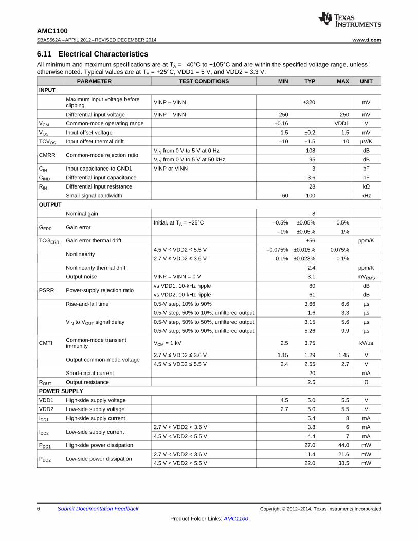
6.11 Electrical CharacteristicsAll minimum and maximum specifications are at TA = –40°C to +105°C and are within the specified voltage range, unlessotherwise noted. Typical values are at TA = +25°C, VDD1 = 5 V, and VDD2 = 3.3 V.
PARAMETER TEST CONDITIONS MIN TYP MAX UNITINPUT
Maximum input voltage before VINP – VINN ±320 mVclippingDifferential input voltage VINP – VINN –250 250 mV
VCM Common-mode operating range –0.16 VDD1 VVOS Input offset voltage –1.5 ±0.2 1.5 mVTCVOS Input offset thermal drift –10 ±1.5 10 µV/K
VIN from 0 V to 5 V at 0 Hz 108 dBCMRR Common-mode rejection ratio
VIN from 0 V to 5 V at 50 kHz 95 dBCIN Input capacitance to GND1 VINP or VINN 3 pFCIND Differential input capacitance 3.6 pFRIN Differential input resistance 28 kΩ
Small-signal bandwidth 60 100 kHzOUTPUT
Nominal gain 8Initial, at TA = +25°C –0.5% ±0.05% 0.5%
GERR Gain error–1% ±0.05% 1%
TCGERR Gain error thermal drift ±56 ppm/K4.5 V ≤ VDD2 ≤ 5.5 V –0.075% ±0.015% 0.075%
Nonlinearity2.7 V ≤ VDD2 ≤ 3.6 V –0.1% ±0.023% 0.1%
Nonlinearity thermal drift 2.4 ppm/KOutput noise VINP = VINN = 0 V 3.1 mVRMS
vs VDD1, 10-kHz ripple 80 dBPSRR Power-supply rejection ratio
vs VDD2, 10-kHz ripple 61 dBRise-and-fall time 0.5-V step, 10% to 90% 3.66 6.6 µs
0.5-V step, 50% to 10%, unfiltered output 1.6 3.3 µsVIN to VOUT signal delay 0.5-V step, 50% to 50%, unfiltered output 3.15 5.6 µs
0.5-V step, 50% to 90%, unfiltered output 5.26 9.9 µsCommon-mode transientCMTI VCM = 1 kV 2.5 3.75 kV/µsimmunity
2.7 V ≤ VDD2 ≤ 3.6 V 1.15 1.29 1.45 VOutput common-mode voltage
4.5 V ≤ VDD2 ≤ 5.5 V 2.4 2.55 2.7 VShort-circuit current 20 mA
ROUT Output resistance 2.5 ΩPOWER SUPPLYVDD1 High-side supply voltage 4.5 5.0 5.5 VVDD2 Low-side supply voltage 2.7 5.0 5.5 VIDD1 High-side supply current 5.4 8 mA
2.7 V < VDD2 < 3.6 V 3.8 6 mAIDD2 Low-side supply current
4.5 V < VDD2 < 5.5 V 4.4 7 mAPDD1 High-side power dissipation 27.0 44.0 mW
2.7 V < VDD2 < 3.6 V 11.4 21.6 mWPDD2 Low-side power dissipation
4.5 V < VDD2 < 5.5 V 22.0 38.5 mW
6 Submit Documentation Feedback Copyright © 2012–2014, Texas Instruments Incorporated
Product Folder Links: AMC1100
50
60
70
80
90
100
110
120
130
0.1 1 10 100Input Frequency (kHz)
CM
RR
(dB
)
−40
−30
−20
−10
0
10
20
30
40
−400 −300 −200 −100 0 100 200 300 400Input Voltage (mV)
Inpu
t Cur
rent
(µA
)
−2
−1.5
−1
−0.5
0
0.5
1
1.5
2
4.5 4.75 5 5.25 5.5VDD2 (V)
Inpu
t Offs
et (
mV
)
VDD2 = 4.5 V to 5.5 V
−2
−1.5
−1
−0.5
0
0.5
1
1.5
2
−40 −25 −10 5 20 35 50 65 80 95 110 125Temperature (°C)
Inpu
t Offs
et (
mV
)
−2
−1.5
−1
−0.5
0
0.5
1
1.5
2
4.5 4.75 5 5.25 5.5VDD1 (V)
Inpu
t Offs
et (
mV
)
−2
−1.5
−1
−0.5
0
0.5
1
1.5
2
2.7 3 3.3 3.6VDD2 (V)
Inpu
t Offs
et (
mV
)
VDD2 = 2.7 V to 3.6 V
AMC1100www.ti.com SBAS562A –APRIL 2012–REVISED DECEMBER 2014
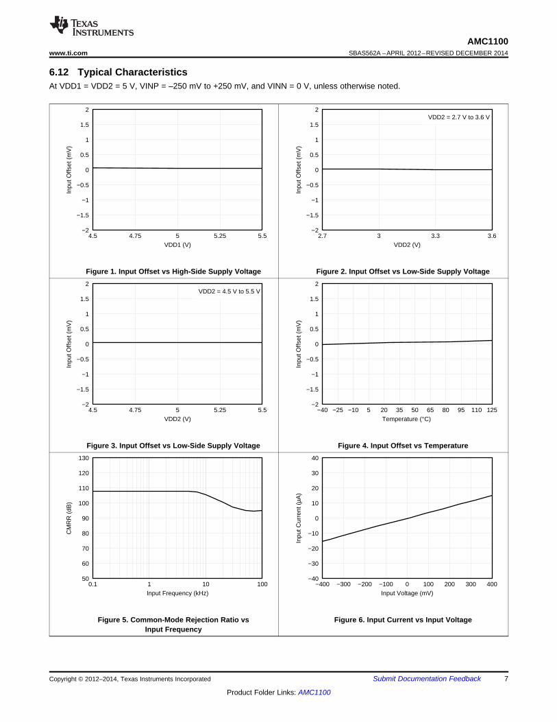
6.12 Typical CharacteristicsAt VDD1 = VDD2 = 5 V, VINP = –250 mV to +250 mV, and VINN = 0 V, unless otherwise noted.
Figure 1. Input Offset vs High-Side Supply Voltage Figure 2. Input Offset vs Low-Side Supply Voltage
Figure 3. Input Offset vs Low-Side Supply Voltage Figure 4. Input Offset vs Temperature
Figure 5. Common-Mode Rejection Ratio vs Figure 6. Input Current vs Input VoltageInput Frequency
Copyright © 2012–2014, Texas Instruments Incorporated Submit Documentation Feedback 7
Product Folder Links: AMC1100
−1
−0.8
−0.6
−0.4
−0.2
0
0.2
0.4
0.6
0.8
1
−40 −25 −10 5 20 35 50 65 80 95 110 125Temperature (°C)
Gai
n E
rror
(%
)
−80
−70
−60
−50
−40
−30
−20
−10
0
10
1 10 100 500Input Frequency (kHz)
Nor
mal
ized
Gai
n (d
B)
−1
−0.8
−0.6
−0.4
−0.2
0
0.2
0.4
0.6
0.8
1
2.7 3 3.3 3.6VDD2 (V)
Gai
n E
rror
(%
)
VDD2 = 2.7 V to 3.6 V
−1
−0.8
−0.6
−0.4
−0.2
0
0.2
0.4
0.6
0.8
1
4.5 4.75 5 5.25 5.5VDD2 (V)
Gai
n E
rror
(%
)
VDD2 = 4.5 V to 5.5 V
60
70
80
90
100
110
120
−40 −25 −10 5 20 35 50 65 80 95 110 125Temperature (°C)
Inpu
t Ban
dwid
th (
kHz)
−1
−0.8
−0.6
−0.4
−0.2
0
0.2
0.4
0.6
0.8
1
4.5 4.75 5 5.25 5.5VDD1 (V)
Gai
n E
rror
(%
)
AMC1100SBAS562A –APRIL 2012–REVISED DECEMBER 2014 www.ti.com
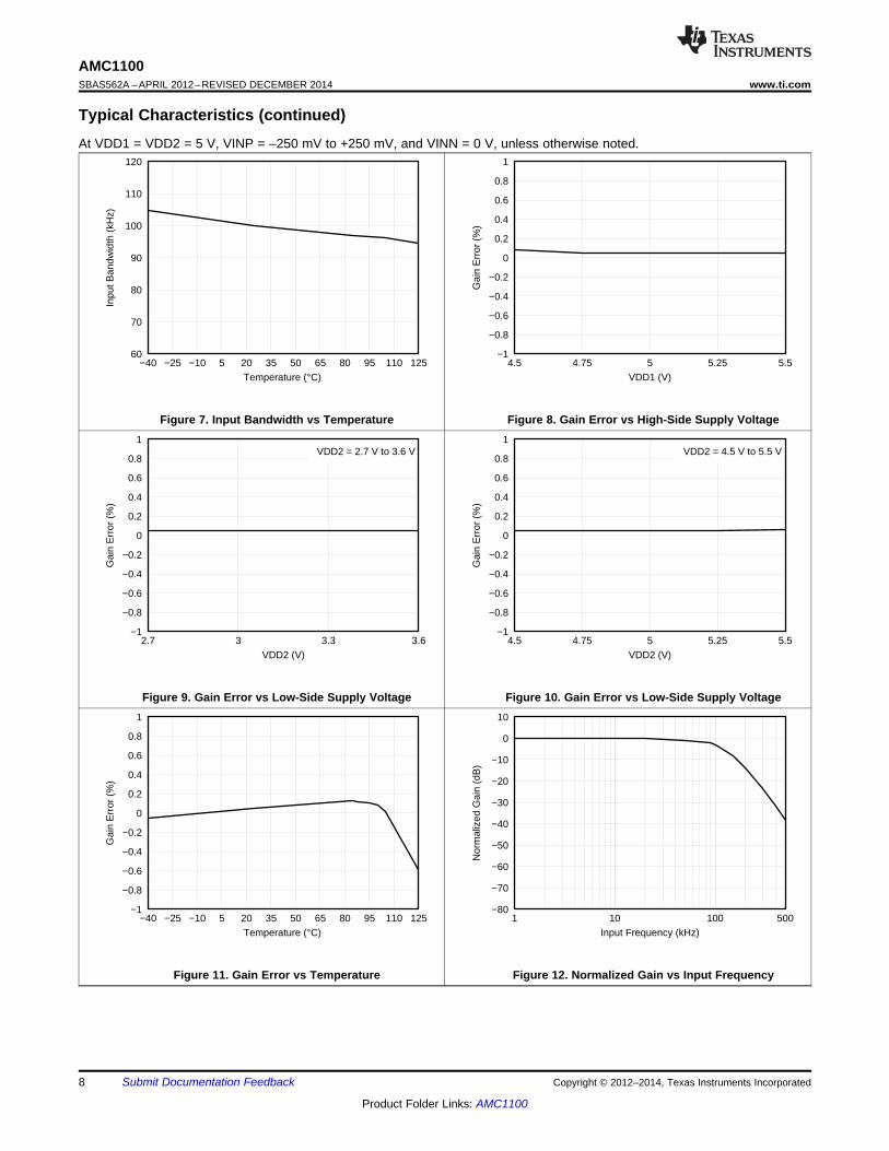
Typical Characteristics (continued)At VDD1 = VDD2 = 5 V, VINP = –250 mV to +250 mV, and VINN = 0 V, unless otherwise noted.
Figure 7. Input Bandwidth vs Temperature Figure 8. Gain Error vs High-Side Supply Voltage
Figure 9. Gain Error vs Low-Side Supply Voltage Figure 10. Gain Error vs Low-Side Supply Voltage
Figure 11. Gain Error vs Temperature Figure 12. Normalized Gain vs Input Frequency
8 Submit Documentation Feedback Copyright © 2012–2014, Texas Instruments Incorporated
Product Folder Links: AMC1100
−0.1
−0.08
−0.06
−0.04
−0.02
0
0.02
0.04
0.06
0.08
0.1
2.7 3 3.3 3.6VDD2 (V)
Non
linea
rity
(%)
VDD2 = 2.7 V to 3.6 V
−0.1
−0.08
−0.06
−0.04
−0.02
0
0.02
0.04
0.06
0.08
0.1
4.5 4.75 5 5.25 5.5VDD2 (V)
Non
linea
rity
(%)
VDD2 = 4.5 V to 5.5 V
0
0.3
0.6
0.9
1.2
1.5
1.8
2.1
2.4
2.7
3
3.3
3.6
−400 −300 −200 −100 0 100 200 300 400Input Voltage (mV)
Out
put V
olta
ge (
V)
VOUTPVOUTN
VDD2 = 2.7 V to 3.6 V
−0.1
−0.08
−0.06
−0.04
−0.02
0
0.02
0.04
0.06
0.08
0.1
4.5 4.75 5 5.25 5.5VDD1 (V)
Non
linea
rity
(%)
−360
−330
−300
−270
−240
−210
−180
−150
−120
−90
−60
−30
0
1 10 100 1000Input Frequency (kHz)
Out
put P
hase
(°)
0
0.5
1
1.5
2
2.5
3
3.5
4
4.5
5
−400 −300 −200 −100 0 100 200 300 400Input Voltage (mV)
Out
put V
olta
ge (
V)
VOUTPVOUTN
AMC1100www.ti.com SBAS562A –APRIL 2012–REVISED DECEMBER 2014
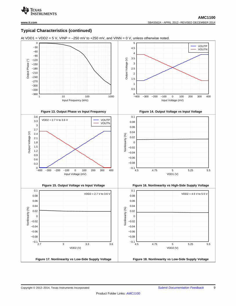
Typical Characteristics (continued)At VDD1 = VDD2 = 5 V, VINP = –250 mV to +250 mV, and VINN = 0 V, unless otherwise noted.
Figure 13. Output Phase vs Input Frequency Figure 14. Output Voltage vs Input Voltage
Figure 15. Output Voltage vs Input Voltage Figure 16. Nonlinearity vs High-Side Supply Voltage
Figure 17. Nonlinearity vs Low-Side Supply Voltage Figure 18. Nonlinearity vs Low-Side Supply Voltage
Copyright © 2012–2014, Texas Instruments Incorporated Submit Documentation Feedback 9
Product Folder Links: AMC1100
Time (2 s/div)m
200 mV/div
500 mV/div
500 mV/div0
1
2
3
4
5
6
7
8
9
10
−40 −25 −10 5 20 35 50 65 80 95 110 125Temperature (°C)
Out
put R
ise/
Fal
l Tim
e (µ
s)
600
800
1000
1200
1400
1600
1800
2000
2200
2400
2600
0.1 1 10 100Frequency (kHz)
Noi
se (
nV/s
qrt(
Hz)
)
0
10
20
30
40
50
60
70
80
90
100
1 10 100Ripple Frequency (kHz)
PS
RR
(dB
)
VDD1VDD2
−0.1
−0.08
−0.06
−0.04
−0.02
0
0.02
0.04
0.06
0.08
0.1
−250 −200 −150 −100 −50 0 50 100 150 200 250Input Voltage (mV)
Non
linea
rity
(%)
VDD2 = 3 VVDD2 = 5 V
−0.1
−0.08
−0.06
−0.04
−0.02
0
0.02
0.04
0.06
0.08
0.1
−40 −25 −10 5 20 35 50 65 80 95 110 125Temperature (°C)
Non
linea
rity
(%)
AMC1100SBAS562A –APRIL 2012–REVISED DECEMBER 2014 www.ti.com
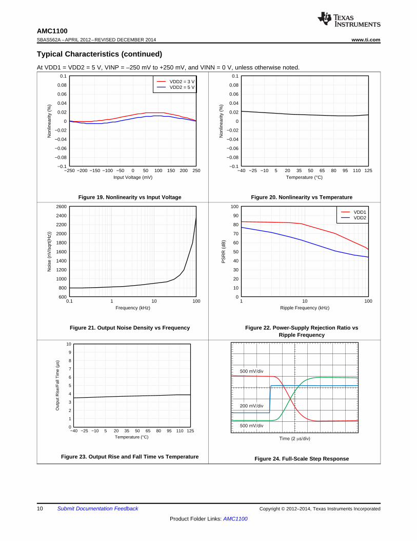
Typical Characteristics (continued)At VDD1 = VDD2 = 5 V, VINP = –250 mV to +250 mV, and VINN = 0 V, unless otherwise noted.
Figure 19. Nonlinearity vs Input Voltage Figure 20. Nonlinearity vs Temperature
Figure 21. Output Noise Density vs Frequency Figure 22. Power-Supply Rejection Ratio vsRipple Frequency
Figure 23. Output Rise and Fall Time vs Temperature Figure 24. Full-Scale Step Response
10 Submit Documentation Feedback Copyright © 2012–2014, Texas Instruments Incorporated
Product Folder Links: AMC1100
0
1
2
3
4
5
6
7
8
2.7 3 3.3 3.6VDD2 (V)
IDD
2 (m
A)
VDD2 = 2.7 V to 3.6 V
0
1
2
3
4
5
6
7
8
−40 −25 −10 5 20 35 50 65 80 95 110 125Temperature (°C)
Sup
ply
Cur
rent
(m
A)
IDD1IDD2
0
1
2
3
4
5
−40 −25 −10 5 20 35 50 65 80 95 110 125Temperature (°C)
Out
put C
omm
on−
Mod
e V
olta
ge (
V) VDD2 = 2.7 V to 3.6 V
VDD2 = 4.5 V to 5.5 V
0
1
2
3
4
5
6
7
8
4.5 4.75 5 5.25 5.5Supply Voltage (V)
Sup
ply
Cur
rent
(m
A)
IDD1IDD2
0
1
2
3
4
5
6
7
8
9
10
−40 −25 −10 5 20 35 50 65 80 95 110 125Temperature (°C)
Sig
nal D
elay
(µs
)
50% to 10%50% to 50%50% to 90%
0
1
2
3
4
5
3.5 3.6 3.7 3.8 3.9 4 4.1 4.2 4.3 4.4 4.5VDD2 (V)
Out
put C
omm
on−
Mod
e V
olta
ge (
V) VDD2 rising
VDD2 falling
AMC1100www.ti.com SBAS562A –APRIL 2012–REVISED DECEMBER 2014
Typical Characteristics (continued)At VDD1 = VDD2 = 5 V, VINP = –250 mV to +250 mV, and VINN = 0 V, unless otherwise noted.
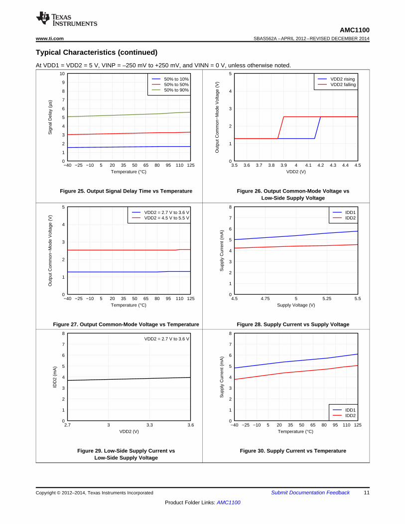
Figure 25. Output Signal Delay Time vs Temperature Figure 26. Output Common-Mode Voltage vsLow-Side Supply Voltage
Figure 27. Output Common-Mode Voltage vs Temperature Figure 28. Supply Current vs Supply Voltage
Figure 29. Low-Side Supply Current vs Figure 30. Supply Current vs TemperatureLow-Side Supply Voltage
Copyright © 2012–2014, Texas Instruments Incorporated Submit Documentation Feedback 11
Product Folder Links: AMC1100
IsolationBarrier
û-Modulator
RX
2.5-VReference
VOUTP
VOUTN
VDD2
GND2GND1
VINP
VINN
VDD1
RC oscillator
RX
TX
TX
Retiming and 3rd order
active low-pass filter
DATA
CLK
2.56-VReference
AMC1100SBAS562A –APRIL 2012–REVISED DECEMBER 2014 www.ti.com
7 Detailed Description
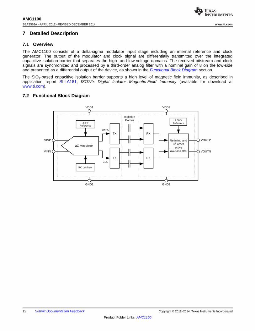
7.1 OverviewThe AMC1100 consists of a delta-sigma modulator input stage including an internal reference and clockgenerator. The output of the modulator and clock signal are differentially transmitted over the integratedcapacitive isolation barrier that separates the high- and low-voltage domains. The received bitstream and clocksignals are synchronized and processed by a third-order analog filter with a nominal gain of 8 on the low-sideand presented as a differential output of the device, as shown in the Functional Block Diagram section.
The SiO2-based capacitive isolation barrier supports a high level of magnetic field immunity, as described inapplication report SLLA181, ISO72x Digital Isolator Magnetic-Field Immunity (available for download atwww.ti.com).
7.2 Functional Block Diagram
12 Submit Documentation Feedback Copyright © 2012–2014, Texas Instruments Incorporated
Product Folder Links: AMC1100
CIND = 3.6 pF
3 pF
CINP = 3 pF
S2
S2
S1
S1
400 :
400 :
CINN = 3 pF
GND1 GND1
GND1VDD1
GND1 + 0.8 V
GND1 + 0.8 V
GND1
RIN = 28 k:
GND1
3 pF
EquivalentCurcuit
INDIN C
R*f
1
CLK
(fCLK = 10 MHz)
AMC1100www.ti.com SBAS562A –APRIL 2012–REVISED DECEMBER 2014
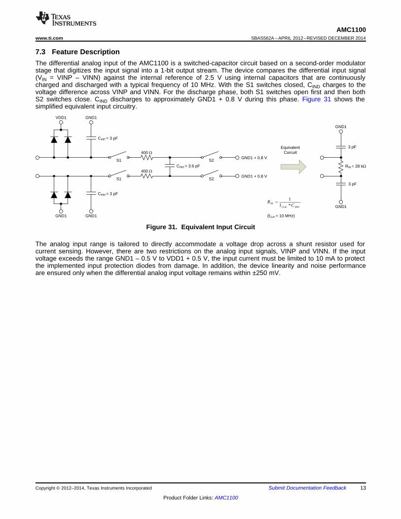
7.3 Feature DescriptionThe differential analog input of the AMC1100 is a switched-capacitor circuit based on a second-order modulatorstage that digitizes the input signal into a 1-bit output stream. The device compares the differential input signal(VIN = VINP – VINN) against the internal reference of 2.5 V using internal capacitors that are continuouslycharged and discharged with a typical frequency of 10 MHz. With the S1 switches closed, CIND charges to thevoltage difference across VINP and VINN. For the discharge phase, both S1 switches open first and then bothS2 switches close. CIND discharges to approximately GND1 + 0.8 V during this phase. Figure 31 shows thesimplified equivalent input circuitry.
Figure 31. Equivalent Input Circuit
The analog input range is tailored to directly accommodate a voltage drop across a shunt resistor used forcurrent sensing. However, there are two restrictions on the analog input signals, VINP and VINN. If the inputvoltage exceeds the range GND1 – 0.5 V to VDD1 + 0.5 V, the input current must be limited to 10 mA to protectthe implemented input protection diodes from damage. In addition, the device linearity and noise performanceare ensured only when the differential analog input voltage remains within ±250 mV.
Copyright © 2012–2014, Texas Instruments Incorporated Submit Documentation Feedback 13
Product Folder Links: AMC1100
RIN
R2
R1
L1
L2
G = G +ERRTOT ERR
R2
RIN
AMC1100SBAS562A –APRIL 2012–REVISED DECEMBER 2014 www.ti.com
7.4 Device Functional ModesThe AMC1100 is powered on when the supplies are connected. The device is operated off a 5-V nominal supplyon the high-side. The potential of the ground reference GND1 can be floating, which is usually the case in shunt-based current-measurement applications. TI recommends tying one side of the shunt to the GND1 pin of theAMC1100 to maintain the operating common-mode range requirements of the device.
The low-side of the AMC1100 can be powered from a supply source with a nominal voltage of 3.0 V, 3.3 V, or5.0 V. When operated at 5 V, the common-mode voltage of the output stage is set to 2.55 V nominal; in bothother cases, the common-mode voltage is automatically set to 1.29 V.
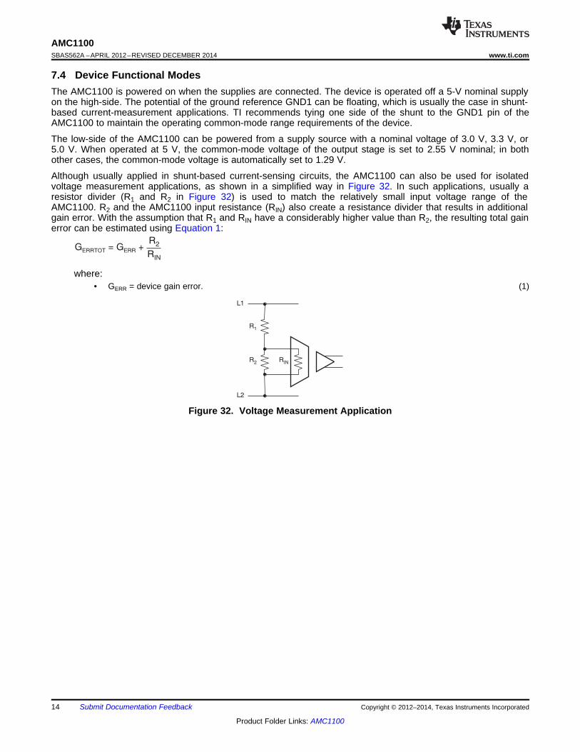
Although usually applied in shunt-based current-sensing circuits, the AMC1100 can also be used for isolatedvoltage measurement applications, as shown in a simplified way in Figure 32. In such applications, usually aresistor divider (R1 and R2 in Figure 32) is used to match the relatively small input voltage range of theAMC1100. R2 and the AMC1100 input resistance (RIN) also create a resistance divider that results in additionalgain error. With the assumption that R1 and RIN have a considerably higher value than R2, the resulting total gainerror can be estimated using Equation 1:
where:• GERR = device gain error. (1)
Figure 32. Voltage Measurement Application
14 Submit Documentation Feedback Copyright © 2012–2014, Texas Instruments Incorporated
Product Folder Links: AMC1100
ADC1N
ADC1P
DC Link
Gate Driver
Gate Driver
Gate Driver
Gate Driver
Gate Driver
Gate Driver
ADC2N
ADC2P
ADC3N
ADC3P
ADC4N
ADC4P
RSHUNT
VOUTP
VOUTN
VDD2
GND2GND1
VINN
VINP
VDD1
AMC1100
VOUTP
VOUTN
VDD2
GND2GND1
VINN
VINP
VDD1
AMC1100
RSHUNT
VOUTP
VOUTN
VDD2
GND2GND1
VINN
VINP
VDD1
AMC1100
RSHUNT
VOUTP
VOUTN
VDD2
GND2GND1
VINN
VINP
VDD1
AMC1100
AMC1100www.ti.com SBAS562A –APRIL 2012–REVISED DECEMBER 2014
8 Application and Implementation
NOTEInformation in the following applications sections is not part of the TI componentspecification, and TI does not warrant its accuracy or completeness. TI’s customers areresponsible for determining suitability of components for their purposes. Customers shouldvalidate and test their design implementation to confirm system functionality.
8.1 Application InformationThe AMC1100 offers unique linearity, high input common-mode rejection, and low dc errors and drift. Thesefeatures make the AMC1100 a robust, high-performance isolation amplifier for industrial applications where usersand subsystems must be protected from high voltage potentials.
8.2 Typical Applications
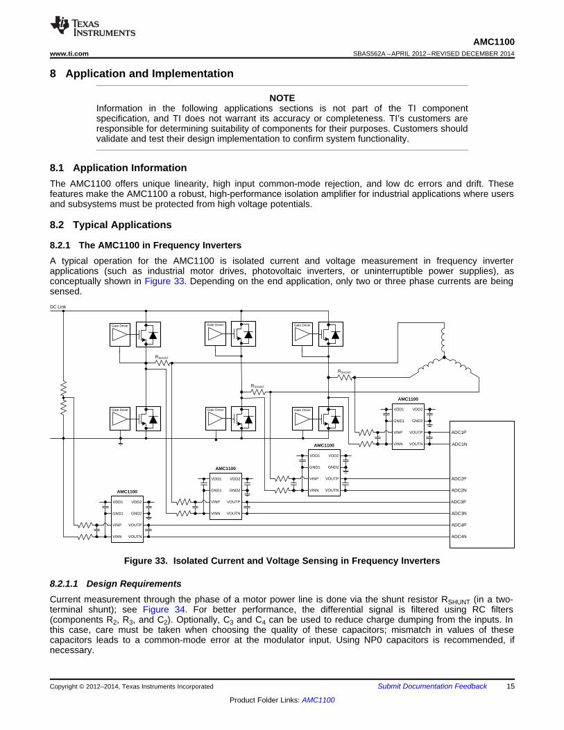
8.2.1 The AMC1100 in Frequency InvertersA typical operation for the AMC1100 is isolated current and voltage measurement in frequency inverterapplications (such as industrial motor drives, photovoltaic inverters, or uninterruptible power supplies), asconceptually shown in Figure 33. Depending on the end application, only two or three phase currents are beingsensed.
Figure 33. Isolated Current and Voltage Sensing in Frequency Inverters
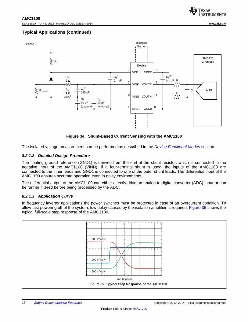
8.2.1.1 Design RequirementsCurrent measurement through the phase of a motor power line is done via the shunt resistor RSHUNT (in a two-terminal shunt); see Figure 34. For better performance, the differential signal is filtered using RC filters(components R2, R3, and C2). Optionally, C3 and C4 can be used to reduce charge dumping from the inputs. Inthis case, care must be taken when choosing the quality of these capacitors; mismatch in values of thesecapacitors leads to a common-mode error at the modulator input. Using NP0 capacitors is recommended, ifnecessary.
Copyright © 2012–2014, Texas Instruments Incorporated Submit Documentation Feedback 15
Product Folder Links: AMC1100
Time (2 s/div)m
200 mV/div
500 mV/div
500 mV/div
R2
12 W
R3
12 W
Device
Isolation
Barrier
C2(1)
330 pF
C3
10 pF
(optional)
VDD1
VINP
VINN
GND1
VDD2
VOUTP
VOUTN
GND2
C4
10 pF
(optional)
C1(1)
0.1 Fm
R1
C5(1)
0.1 Fm
ADC
TMC320
C/F28xxx
C
14
13
11
9
1
2
3
4
R
RRSHUNT
Phase
AMC1100SBAS562A –APRIL 2012–REVISED DECEMBER 2014 www.ti.com
Typical Applications (continued)
Figure 34. Shunt-Based Current Sensing with the AMC1100
The isolated voltage measurement can be performed as described in the Device Functional Modes section.
8.2.1.2 Detailed Design ProcedureThe floating ground reference (GND1) is derived from the end of the shunt resistor, which is connected to thenegative input of the AMC1100 (VINN). If a four-terminal shunt is used, the inputs of the AMC1100 areconnected to the inner leads and GND1 is connected to one of the outer shunt leads. The differential input of theAMC1100 ensures accurate operation even in noisy environments.
The differential output of the AMC1100 can either directly drive an analog-to-digital converter (ADC) input or canbe further filtered before being processed by the ADC.
8.2.1.3 Application CurveIn frequency inverter applications the power switches must be protected in case of an overcurrent condition. Toallow fast powering off of the system, low delay caused by the isolation amplifier is required. Figure 35 shows thetypical full-scale step response of the AMC1100.
Figure 35. Typical Step Response of the AMC1100
16 Submit Documentation Feedback Copyright © 2012–2014, Texas Instruments Incorporated
Product Folder Links: AMC1100
Application
MCU
L1
L2
L3
3x dig. filter for
currents
3x dig. filter for
voltage
Sync
SysCLK
Data
DVDD
N
Digital Core
AMC1100
AMC1100
AMC1100
ADC
ADC
ADC
ADC
ADC
ADC
4G-Modulator
VDD2 = DVDD
VDD1A
VDD1B
VDD1C
MSP430F47167
Metrology
MCU
AMC1100www.ti.com SBAS562A –APRIL 2012–REVISED DECEMBER 2014
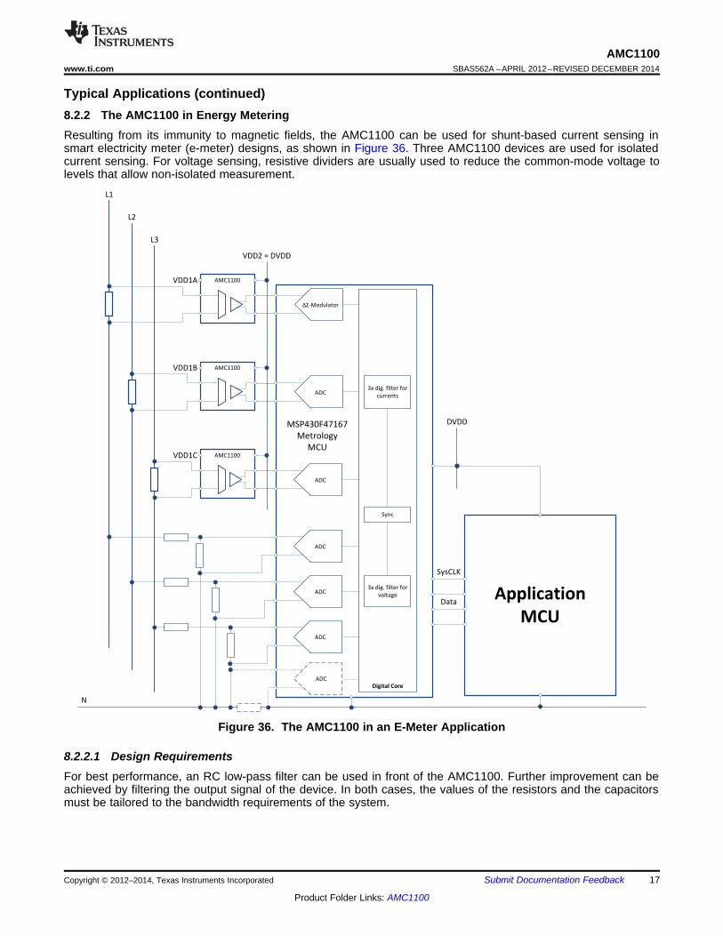
Typical Applications (continued)8.2.2 The AMC1100 in Energy MeteringResulting from its immunity to magnetic fields, the AMC1100 can be used for shunt-based current sensing insmart electricity meter (e-meter) designs, as shown in Figure 36. Three AMC1100 devices are used for isolatedcurrent sensing. For voltage sensing, resistive dividers are usually used to reduce the common-mode voltage tolevels that allow non-isolated measurement.
Figure 36. The AMC1100 in an E-Meter Application
8.2.2.1 Design RequirementsFor best performance, an RC low-pass filter can be used in front of the AMC1100. Further improvement can beachieved by filtering the output signal of the device. In both cases, the values of the resistors and the capacitorsmust be tailored to the bandwidth requirements of the system.
Copyright © 2012–2014, Texas Instruments Incorporated Submit Documentation Feedback 17
Product Folder Links: AMC1100
600
800
1000
1200
1400
1600
1800
2000
2200
2400
2600
0.1 1 10 100Frequency (kHz)
Noi
se (
nV/s
qrt(
Hz)
)
GND
470 n / 400 V 220
5.6V
1N4007
470 µ / 10 V
5.1 VPhase
Neutral
AMC1100SBAS562A –APRIL 2012–REVISED DECEMBER 2014 www.ti.com
Typical Applications (continued)The analog output of the device is converted to the digital domain using the on-chip analog-to-digital converters(ADCs) of a suitable metrology microcontroller. The architecture of the MSP430F471x7 family of ultra-low powermicrocontrollers is tailored for this kind of applications. The MSP430F471x7 offers up to seven ADCs forsimultaneous sampling: six of which are used for the three phase currents and voltages whereas the seventhchannel can be used for additional voltage sensing of the neutral line for applications that require anti-tamperingmeasures.
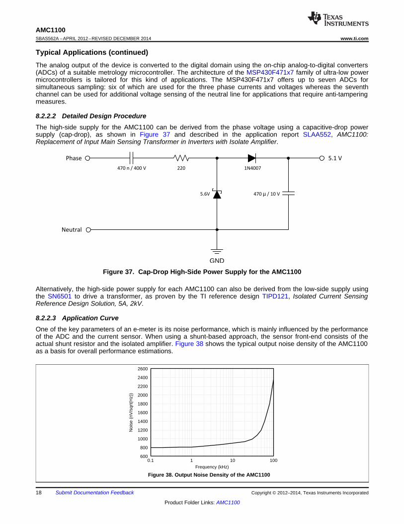
8.2.2.2 Detailed Design ProcedureThe high-side supply for the AMC1100 can be derived from the phase voltage using a capacitive-drop powersupply (cap-drop), as shown in Figure 37 and described in the application report SLAA552, AMC1100:Replacement of Input Main Sensing Transformer in Inverters with Isolate Amplifier.
Figure 37. Cap-Drop High-Side Power Supply for the AMC1100
Alternatively, the high-side power supply for each AMC1100 can also be derived from the low-side supply usingthe SN6501 to drive a transformer, as proven by the TI reference design TIPD121, Isolated Current SensingReference Design Solution, 5A, 2kV.
8.2.2.3 Application CurveOne of the key parameters of an e-meter is its noise performance, which is mainly influenced by the performanceof the ADC and the current sensor. When using a shunt-based approach, the sensor front-end consists of theactual shunt resistor and the isolated amplifier. Figure 38 shows the typical output noise density of the AMC1100as a basis for overall performance estimations.
Figure 38. Output Noise Density of the AMC1100
18 Submit Documentation Feedback Copyright © 2012–2014, Texas Instruments Incorporated
Product Folder Links: AMC1100
VOUTP
VOUTN
VDD2
GND2GND1
VINN
VINP
VDD1
AMC1100
HV+
HV-
to load
FloatingPower Supply
20 V
3.3 V, or 5.0 V
RSHUNT
Gate Driver
Gate Driver
5.1 V
R1800
Z11N751A
C10.1F
R212
R312
C3330pF
C40.1F
ADS7263
AMC1100www.ti.com SBAS562A –APRIL 2012–REVISED DECEMBER 2014
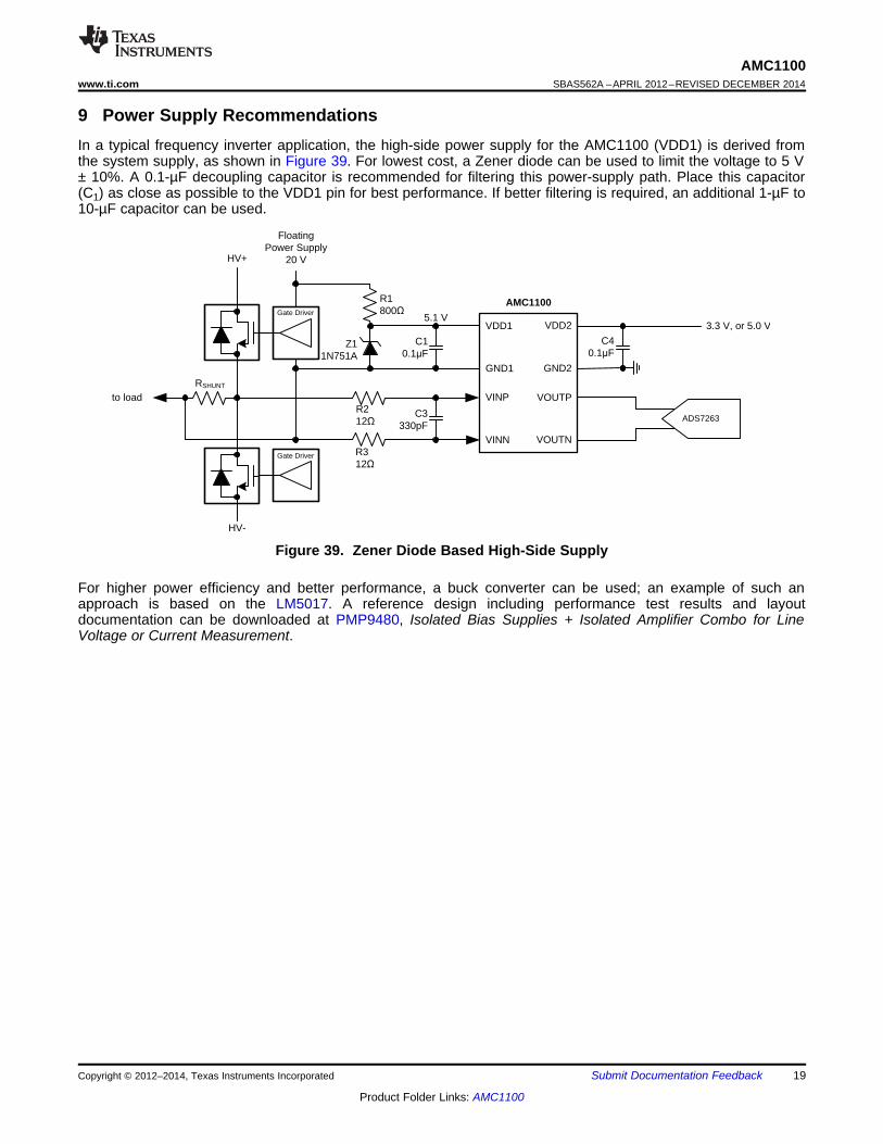
9 Power Supply RecommendationsIn a typical frequency inverter application, the high-side power supply for the AMC1100 (VDD1) is derived fromthe system supply, as shown in Figure 39. For lowest cost, a Zener diode can be used to limit the voltage to 5 V± 10%. A 0.1-µF decoupling capacitor is recommended for filtering this power-supply path. Place this capacitor(C1) as close as possible to the VDD1 pin for best performance. If better filtering is required, an additional 1-µF to10-µF capacitor can be used.
Figure 39. Zener Diode Based High-Side Supply
For higher power efficiency and better performance, a buck converter can be used; an example of such anapproach is based on the LM5017. A reference design including performance test results and layoutdocumentation can be downloaded at PMP9480, Isolated Bias Supplies + Isolated Amplifier Combo for LineVoltage or Current Measurement.
Copyright © 2012–2014, Texas Instruments Incorporated Submit Documentation Feedback 19
Product Folder Links: AMC1100
Top View
Clearance area.
Keep free of any
conductive materials.
Device
LEGEND
Top layer; copper pour and traces
High-side area
Controller-side area
Via
To Shunt To Filter or ADC
VDD1
VINP
GND1
VINN
VDD2
VOUTP
VOUTN
GND2
0.1mF
SMD
1206
0.1 F
SMD
1206
m0.1 F
SMD
1206
m330 pF
SMD
0603
12
SMD 0603
W
12
SMD 0603
W
AMC1100SBAS562A –APRIL 2012–REVISED DECEMBER 2014 www.ti.com
10 Layout
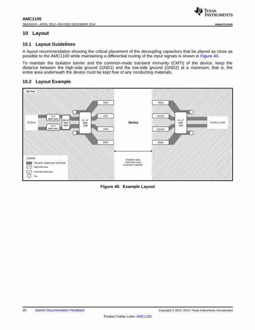
10.1 Layout GuidelinesA layout recommendation showing the critical placement of the decoupling capacitors that be placed as close aspossible to the AMC1100 while maintaining a differential routing of the input signals is shown in Figure 40.
To maintain the isolation barrier and the common-mode transient immunity (CMTI) of the device, keep thedistance between the high-side ground (GND1) and the low-side ground (GND2) at a maximum; that is, theentire area underneath the device must be kept free of any conducting materials.
10.2 Layout Example
Figure 40. Example Layout
20 Submit Documentation Feedback Copyright © 2012–2014, Texas Instruments Incorporated
Product Folder Links: AMC1100
AMC1100www.ti.com SBAS562A –APRIL 2012–REVISED DECEMBER 2014
11 Device and Documentation Support
11.1 Device Support
11.1.1 Device Nomenclature
11.1.1.1 Isolation GlossaryCreepage Distance: The shortest path between two conductive input-to-output leads measured along thesurface of the insulation. The shortest distance path is found around the end of the package body.
Clearance: The shortest distance between two conductive input-to-output leads measured through air (line ofsight).
Input-to-Output Barrier Capacitance: The total capacitance between all input terminals connected together,and all output terminals connected together.
Input-to-Output Barrier Resistance: The total resistance between all input terminals connected together, andall output terminals connected together.
Primary Circuit: An internal circuit directly connected to an external supply mains or other equivalent source thatsupplies the primary circuit electric power.
Secondary Circuit: A circuit with no direct connection to primary power that derives its power from a separateisolated source.
Comparative Tracking Index (CTI): CTI is an index used for electrical insulating materials. It is defined as thenumerical value of the voltage that causes failure by tracking during standard testing. Tracking is the process thatproduces a partially conducting path of localized deterioration on or through the surface of an insulating materialas a result of the action of electric discharges on or close to an insulation surface. The higher CTI value of theinsulating material, the smaller the minimum creepage distance.
Generally, insulation breakdown occurs either through the material, over its surface, or both. Surface failure mayarise from flashover or from the progressive insulation surface degradation by small localized sparks. Suchsparks result from a surface film of a conducting contaminant breaking on the insulation. The resulting break inthe leakage current produces an overvoltage at the site of the discontinuity, and an electric spark is generated.These sparks often cause carbonization on insulation material and lead to a carbon track between points ofdifferent potential. This process is known as tracking.
11.1.1.1.1 Insulation:
Operational insulation—Insulation needed for correct equipment operation.
Basic insulation—Insulation to provide basic protection against electric shock.
Supplementary insulation—Independent insulation applied in addition to basic insulation in order to ensureprotection against electric shock in the event of a failure of the basic insulation.
Copyright © 2012–2014, Texas Instruments Incorporated Submit Documentation Feedback 21
Product Folder Links: AMC1100
AMC1100SBAS562A –APRIL 2012–REVISED DECEMBER 2014 www.ti.com
Device Support (continued)Double insulation—Insulation comprising both basic and supplementary insulation.
Reinforced insulation—A single insulation system that provides a degree of protection against electric shockequivalent to double insulation.
11.1.1.1.2 Pollution Degree:
Pollution Degree 1—No pollution, or only dry, nonconductive pollution occurs. The pollution has no influence ondevice performance.
Pollution Degree 2—Normally, only nonconductive pollution occurs. However, a temporary conductivity causedby condensation is to be expected.
Pollution Degree 3—Conductive pollution, or dry nonconductive pollution that becomes conductive because ofcondensation, occurs. Condensation is to be expected.
Pollution Degree 4—Continuous conductivity occurs as a result of conductive dust, rain, or other wet conditions.
11.1.1.1.3 Installation Category:
Overvoltage Category—This section is directed at insulation coordination by identifying the transient overvoltagesthat may occur, and by assigning four different levels as indicated in IEC 60664.1. Signal Level: Special equipment or parts of equipment.2. Local Level: Portable equipment and so forth3. Distribution Level: Fixed installation.4. Primary Supply Level: Overhead lines, cable systems.
Each category should be subject to smaller transients than the previous category.
22 Submit Documentation Feedback Copyright © 2012–2014, Texas Instruments Incorporated
Product Folder Links: AMC1100
AMC1100www.ti.com SBAS562A –APRIL 2012–REVISED DECEMBER 2014
11.2 Documentation Support
11.2.1 Related DocumentationHigh-Voltage Lifetime of the ISO72x Family of Digital Isolators, SLLA197
ISO72x Digital Isolator Magnetic-Field Immunity, SLLA181
AMC1100: Replacement of Input Main Sensing Transformer in Inverters with Isolate Amplifier, SLAA552
Isolated Current Sensing Reference Design Solution, 5A, 2kV, TIPD121
Isolated Bias Supplies + Isolated Amplifier Combo for Line Voltage or Current Measurement, PMP9480
TPS62120 Data Sheet, SLVSAD5
MSP430F471xx Data Sheet, SLAS626
SN6501 Data Sheet, SLLSEA0
LM5017 Data Sheet, SNVS783
11.3 TrademarksAll trademarks are the property of their respective owners.
11.4 Electrostatic Discharge CautionThis integrated circuit can be damaged by ESD. Texas Instruments recommends that all integrated circuits be handled withappropriate precautions. Failure to observe proper handling and installation procedures can cause damage.
ESD damage can range from subtle performance degradation to complete device failure. Precision integrated circuits may be moresusceptible to damage because very small parametric changes could cause the device not to meet its published specifications.
11.5 GlossarySLYZ022 — TI Glossary.
This glossary lists and explains terms, acronyms, and definitions.
12 Mechanical, Packaging, and Orderable InformationThe following pages include mechanical, packaging, and orderable information. This information is the mostcurrent data available for the designated devices. This data is subject to change without notice and revision ofthis document. For browser-based versions of this data sheet, refer to the left-hand navigation.
Copyright © 2012–2014, Texas Instruments Incorporated Submit Documentation Feedback 23
Product Folder Links: AMC1100
PACKAGE OPTION ADDENDUM
www.ti.com 17-Dec-2014
Addendum-Page 1
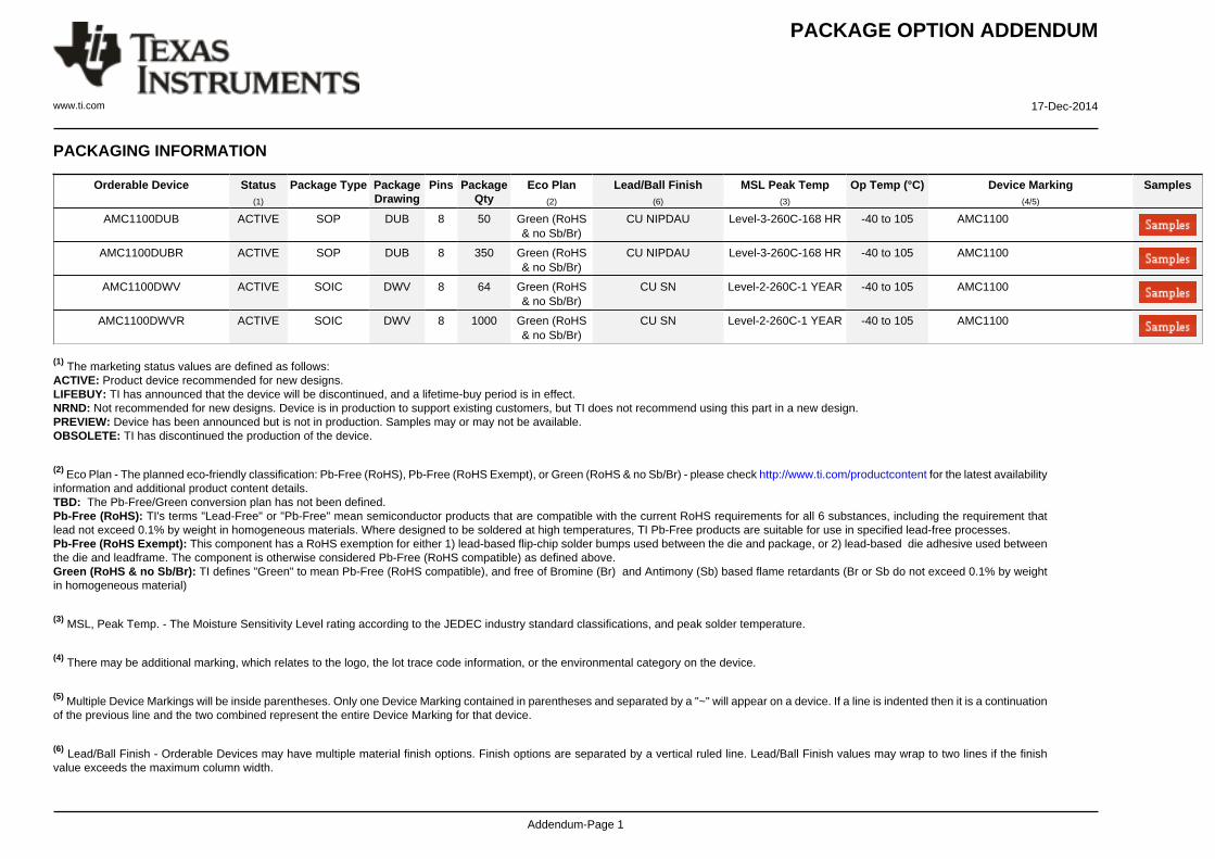
PACKAGING INFORMATION
Orderable Device Status(1)
Package Type PackageDrawing
Pins PackageQty
Eco Plan(2)
Lead/Ball Finish(6)
MSL Peak Temp(3)
Op Temp (°C) Device Marking(4/5)
Samples
AMC1100DUB ACTIVE SOP DUB 8 50 Green (RoHS& no Sb/Br)
CU NIPDAU Level-3-260C-168 HR -40 to 105 AMC1100
AMC1100DUBR ACTIVE SOP DUB 8 350 Green (RoHS& no Sb/Br)
CU NIPDAU Level-3-260C-168 HR -40 to 105 AMC1100
AMC1100DWV ACTIVE SOIC DWV 8 64 Green (RoHS& no Sb/Br)
CU SN Level-2-260C-1 YEAR -40 to 105 AMC1100
AMC1100DWVR ACTIVE SOIC DWV 8 1000 Green (RoHS& no Sb/Br)
CU SN Level-2-260C-1 YEAR -40 to 105 AMC1100
(1) The marketing status values are defined as follows:ACTIVE: Product device recommended for new designs.LIFEBUY: TI has announced that the device will be discontinued, and a lifetime-buy period is in effect.NRND: Not recommended for new designs. Device is in production to support existing customers, but TI does not recommend using this part in a new design.PREVIEW: Device has been announced but is not in production. Samples may or may not be available.OBSOLETE: TI has discontinued the production of the device.
(2) Eco Plan - The planned eco-friendly classification: Pb-Free (RoHS), Pb-Free (RoHS Exempt), or Green (RoHS & no Sb/Br) - please check http://www.ti.com/productcontent for the latest availabilityinformation and additional product content details.TBD: The Pb-Free/Green conversion plan has not been defined.Pb-Free (RoHS): TI's terms "Lead-Free" or "Pb-Free" mean semiconductor products that are compatible with the current RoHS requirements for all 6 substances, including the requirement thatlead not exceed 0.1% by weight in homogeneous materials. Where designed to be soldered at high temperatures, TI Pb-Free products are suitable for use in specified lead-free processes.Pb-Free (RoHS Exempt): This component has a RoHS exemption for either 1) lead-based flip-chip solder bumps used between the die and package, or 2) lead-based die adhesive used betweenthe die and leadframe. The component is otherwise considered Pb-Free (RoHS compatible) as defined above.Green (RoHS & no Sb/Br): TI defines "Green" to mean Pb-Free (RoHS compatible), and free of Bromine (Br) and Antimony (Sb) based flame retardants (Br or Sb do not exceed 0.1% by weightin homogeneous material)
(3) MSL, Peak Temp. - The Moisture Sensitivity Level rating according to the JEDEC industry standard classifications, and peak solder temperature.
(4) There may be additional marking, which relates to the logo, the lot trace code information, or the environmental category on the device.
(5) Multiple Device Markings will be inside parentheses. Only one Device Marking contained in parentheses and separated by a "~" will appear on a device. If a line is indented then it is a continuationof the previous line and the two combined represent the entire Device Marking for that device.
(6) Lead/Ball Finish - Orderable Devices may have multiple material finish options. Finish options are separated by a vertical ruled line. Lead/Ball Finish values may wrap to two lines if the finishvalue exceeds the maximum column width.
PACKAGE OPTION ADDENDUM
www.ti.com 17-Dec-2014
Addendum-Page 2
Important Information and Disclaimer:The information provided on this page represents TI's knowledge and belief as of the date that it is provided. TI bases its knowledge and belief on informationprovided by third parties, and makes no representation or warranty as to the accuracy of such information. Efforts are underway to better integrate information from third parties. TI has taken andcontinues to take reasonable steps to provide representative and accurate information but may not have conducted destructive testing or chemical analysis on incoming materials and chemicals.TI and TI suppliers consider certain information to be proprietary, and thus CAS numbers and other limited information may not be available for release.
In no event shall TI's liability arising out of such information exceed the total purchase price of the TI part(s) at issue in this document sold by TI to Customer on an annual basis.
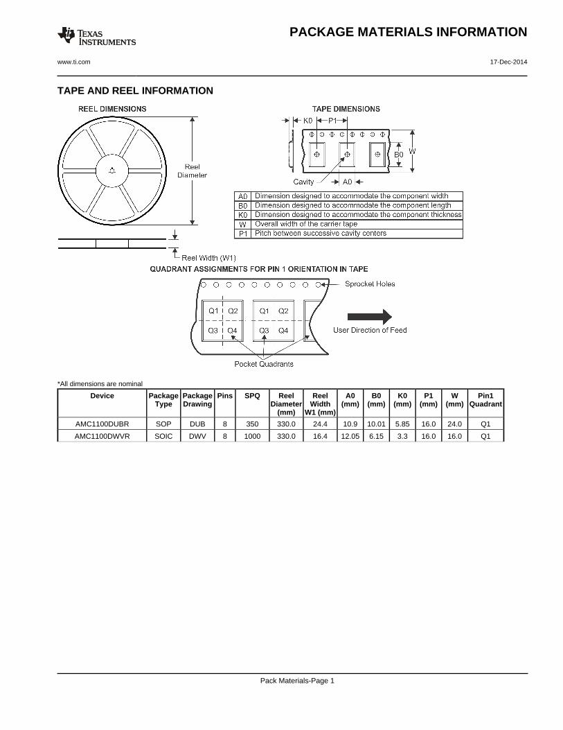
TAPE AND REEL INFORMATION
*All dimensions are nominal
Device PackageType
PackageDrawing
Pins SPQ ReelDiameter
(mm)
ReelWidth
W1 (mm)
A0(mm)
B0(mm)
K0(mm)
P1(mm)
W(mm)
Pin1Quadrant
AMC1100DUBR SOP DUB 8 350 330.0 24.4 10.9 10.01 5.85 16.0 24.0 Q1
AMC1100DWVR SOIC DWV 8 1000 330.0 16.4 12.05 6.15 3.3 16.0 16.0 Q1
PACKAGE MATERIALS INFORMATION
www.ti.com 17-Dec-2014
Pack Materials-Page 1
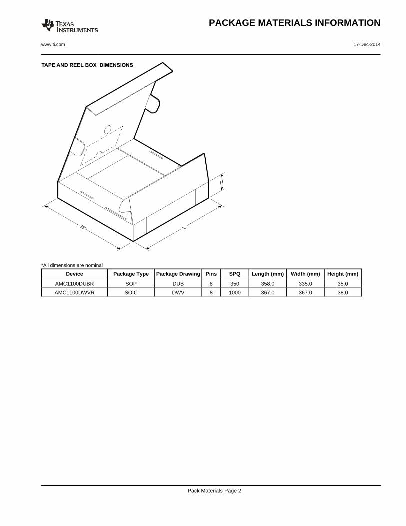
*All dimensions are nominal
Device Package Type Package Drawing Pins SPQ Length (mm) Width (mm) Height (mm)
AMC1100DUBR SOP DUB 8 350 358.0 335.0 35.0
AMC1100DWVR SOIC DWV 8 1000 367.0 367.0 38.0
PACKAGE MATERIALS INFORMATION
www.ti.com 17-Dec-2014
Pack Materials-Page 2
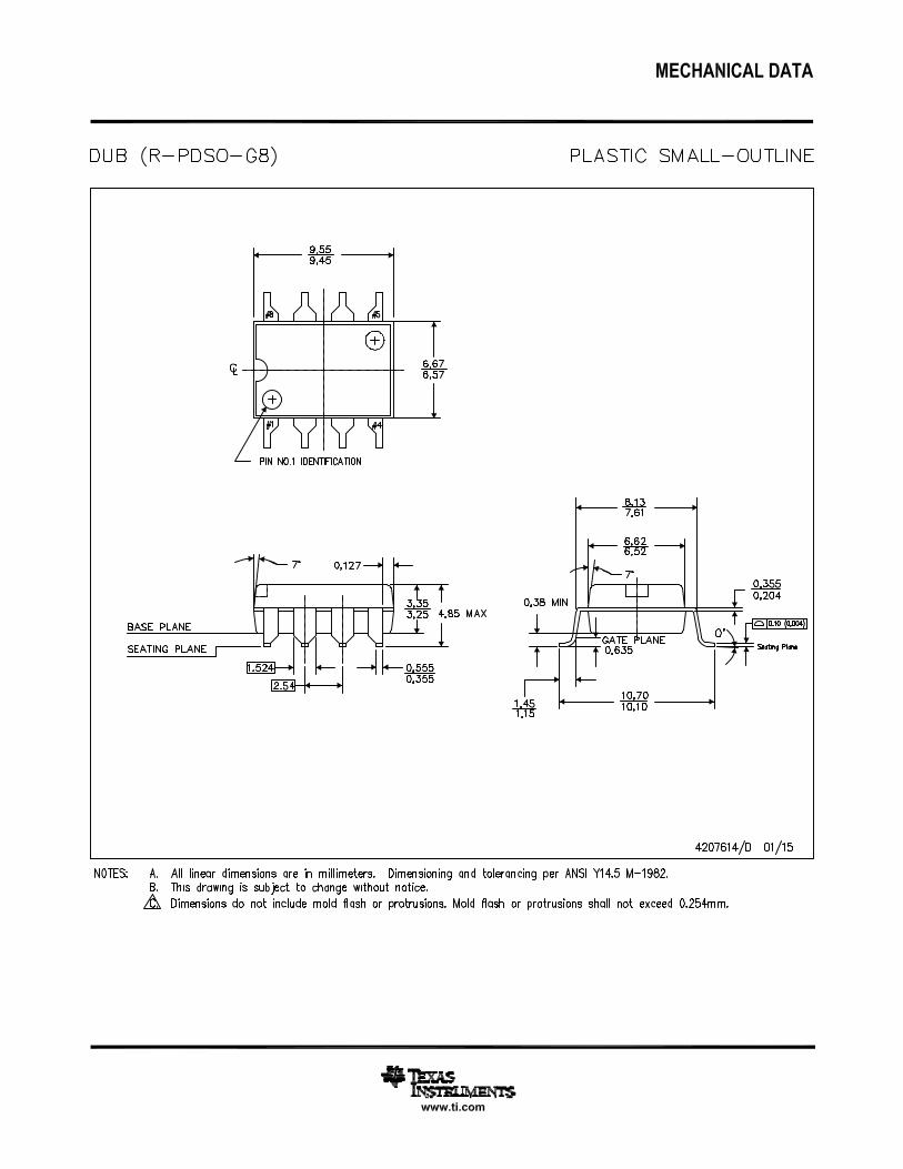
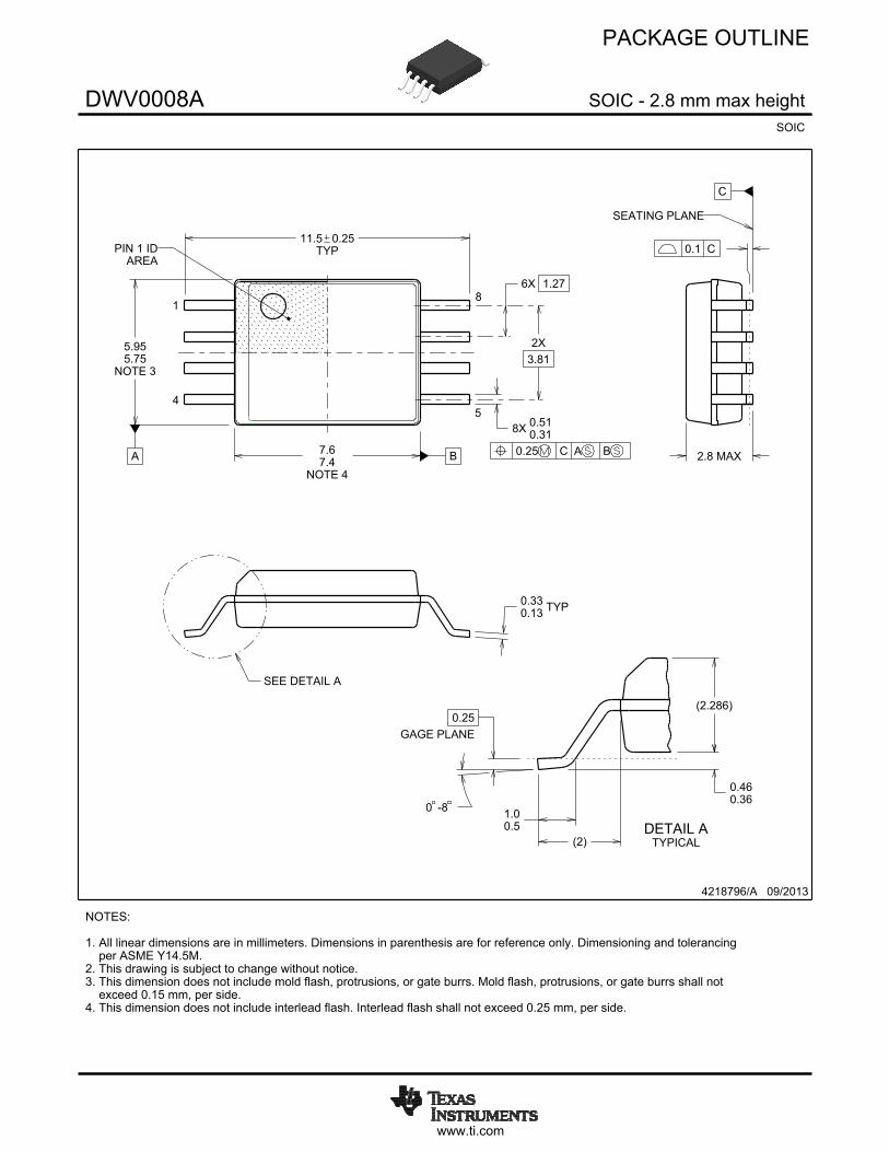
www.ti.com
PACKAGE OUTLINE
C
TYP11.5 0.25
2.8 MAX
TYP0.330.13
0 -8
6X 1.27
8X 0.510.31
2X3.81
0.460.36
1.00.5
0.25GAGE PLANE
A
NOTE 3
5.955.75
BNOTE 4
7.67.4
(2.286)
(2)
4218796/A 09/2013
SOIC - 2.8 mm max heightDWV0008ASOIC
NOTES: 1. All linear dimensions are in millimeters. Dimensions in parenthesis are for reference only. Dimensioning and tolerancing per ASME Y14.5M. 2. This drawing is subject to change without notice. 3. This dimension does not include mold flash, protrusions, or gate burrs. Mold flash, protrusions, or gate burrs shall not exceed 0.15 mm, per side. 4. This dimension does not include interlead flash. Interlead flash shall not exceed 0.25 mm, per side.
18
0.25 C A B
54
AREAPIN 1 ID
SEATING PLANE
0.1 C
SEE DETAIL A
DETAIL ATYPICAL
SCALE 2.000
www.ti.com
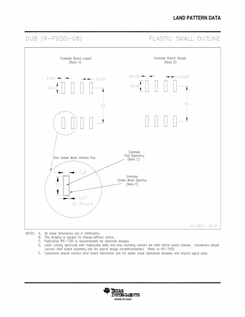
EXAMPLE BOARD LAYOUT
(10.9)
0.07 MAXALL AROUND
0.07 MINALL AROUND
8X (1.8)
8X (0.6)
6X (1.27)
4218796/A 09/2013
SOIC - 2.8 mm max heightDWV0008ASOIC
SYMM
SYMM
SEE DETAILS
LAND PATTERN EXAMPLE9.1 mm NOMINAL CLEARANCE/CREEPAGE
SCALE:6X
NOTES: (continued) 5. Publication IPC-7351 may have alternate designs. 6. Solder mask tolerances between and around signal pads can vary based on board fabrication site.
METAL SOLDER MASKOPENING
NON SOLDER MASKDEFINED
SOLDER MASK DETAILS
OPENINGSOLDER MASK METAL
SOLDER MASKDEFINED
www.ti.com
EXAMPLE STENCIL DESIGN
8X (1.8)
8X (0.6)
6X (1.27)
(10.9)
4218796/A 09/2013
SOIC - 2.8 mm max heightDWV0008ASOIC
NOTES: (continued) 7. Laser cutting apertures with trapezoidal walls and rounded corners may offer better paste release. IPC-7525 may have alternate design recommendations. 8. Board assembly site may have different recommendations for stencil design.
SOLDER PASTE EXAMPLEBASED ON 0.125 mm THICK STENCIL
SCALE:6X
SYMM
SYMM
IMPORTANT NOTICE
Texas Instruments Incorporated and its subsidiaries (TI) reserve the right to make corrections, enhancements, improvements and otherchanges to its semiconductor products and services per JESD46, latest issue, and to discontinue any product or service per JESD48, latestissue. Buyers should obtain the latest relevant information before placing orders and should verify that such information is current andcomplete. All semiconductor products (also referred to herein as “components”) are sold subject to TI’s terms and conditions of salesupplied at the time of order acknowledgment.TI warrants performance of its components to the specifications applicable at the time of sale, in accordance with the warranty in TI’s termsand conditions of sale of semiconductor products. Testing and other quality control techniques are used to the extent TI deems necessaryto support this warranty. Except where mandated by applicable law, testing of all parameters of each component is not necessarilyperformed.TI assumes no liability for applications assistance or the design of Buyers’ products. Buyers are responsible for their products andapplications using TI components. To minimize the risks associated with Buyers’ products and applications, Buyers should provideadequate design and operating safeguards.TI does not warrant or represent that any license, either express or implied, is granted under any patent right, copyright, mask work right, orother intellectual property right relating to any combination, machine, or process in which TI components or services are used. Informationpublished by TI regarding third-party products or services does not constitute a license to use such products or services or a warranty orendorsement thereof. Use of such information may require a license from a third party under the patents or other intellectual property of thethird party, or a license from TI under the patents or other intellectual property of TI.Reproduction of significant portions of TI information in TI data books or data sheets is permissible only if reproduction is without alterationand is accompanied by all associated warranties, conditions, limitations, and notices. TI is not responsible or liable for such altereddocumentation. Information of third parties may be subject to additional restrictions.Resale of TI components or services with statements different from or beyond the parameters stated by TI for that component or servicevoids all express and any implied warranties for the associated TI component or service and is an unfair and deceptive business practice.TI is not responsible or liable for any such statements.Buyer acknowledges and agrees that it is solely responsible for compliance with all legal, regulatory and safety-related requirementsconcerning its products, and any use of TI components in its applications, notwithstanding any applications-related information or supportthat may be provided by TI. Buyer represents and agrees that it has all the necessary expertise to create and implement safeguards whichanticipate dangerous consequences of failures, monitor failures and their consequences, lessen the likelihood of failures that might causeharm and take appropriate remedial actions. Buyer will fully indemnify TI and its representatives against any damages arising out of the useof any TI components in safety-critical applications.In some cases, TI components may be promoted specifically to facilitate safety-related applications. With such components, TI’s goal is tohelp enable customers to design and create their own end-product solutions that meet applicable functional safety standards andrequirements. Nonetheless, such components are subject to these terms.No TI components are authorized for use in FDA Class III (or similar life-critical medical equipment) unless authorized officers of the partieshave executed a special agreement specifically governing such use.Only those TI components which TI has specifically designated as military grade or “enhanced plastic” are designed and intended for use inmilitary/aerospace applications or environments. Buyer acknowledges and agrees that any military or aerospace use of TI componentswhich have not been so designated is solely at the Buyer's risk, and that Buyer is solely responsible for compliance with all legal andregulatory requirements in connection with such use.TI has specifically designated certain components as meeting ISO/TS16949 requirements, mainly for automotive use. In any case of use ofnon-designated products, TI will not be responsible for any failure to meet ISO/TS16949.
Products ApplicationsAudio www.ti.com/audio Automotive and Transportation www.ti.com/automotiveAmplifiers amplifier.ti.com Communications and Telecom www.ti.com/communicationsData Converters dataconverter.ti.com Computers and Peripherals www.ti.com/computersDLP® Products www.dlp.com Consumer Electronics www.ti.com/consumer-appsDSP dsp.ti.com Energy and Lighting www.ti.com/energyClocks and Timers www.ti.com/clocks Industrial www.ti.com/industrialInterface interface.ti.com Medical www.ti.com/medicalLogic logic.ti.com Security www.ti.com/securityPower Mgmt power.ti.com Space, Avionics and Defense www.ti.com/space-avionics-defenseMicrocontrollers microcontroller.ti.com Video and Imaging www.ti.com/videoRFID www.ti-rfid.comOMAP Applications Processors www.ti.com/omap TI E2E Community e2e.ti.comWireless Connectivity www.ti.com/wirelessconnectivity
Mailing Address: Texas Instruments, Post Office Box 655303, Dallas, Texas 75265Copyright © 2015, Texas Instruments Incorporated