Embed Size (px)
Citation preview

Note: no CLKOUT connection using AMC1303Ex, pin 7 to be connected to DGND in this case
DOUT
CLKOUT
DVDD
DGNDAGND
AINP
AINN
AVDD
AMC1303Mx
HV+
HV-
FloatingPower Supply
3.0 V, 3.3 V, or 5.0 V
RSHUNT
3.3 V or 5.0 V
Rei
nfor
ced
Isol
atio
n
SD-Cx
SD-Dx
TMS320F28x7x
Product
Folder
Order
Now
Technical
Documents
Tools &
Software
Support &Community
An IMPORTANT NOTICE at the end of this data sheet addresses availability, warranty, changes, use in safety-critical applications,intellectual property matters and other important disclaimers. PRODUCTION DATA.
AMC1303E0510, AMC1303M0510, AMC1303E0520, AMC1303M0520AMC1303E2510, AMC1303M2510, AMC1303E2520, AMC1303M2520
SBAS771B –JUNE 2017–REVISED JUNE 2018
AMC1303x Small, High-Precision,Reinforced Isolated Delta-Sigma Modulators With Internal Clock
1
1 Features1• Pin-Compatible Family Optimized for Shunt-
Resistor-Based Current Measurements:– ±50-mV or ±250-mV Input Voltage Ranges– Manchester Coded or Uncoded Bistream
Options– 10-MHz and 20-MHz Clock Options
• Excellent DC Performance:– Offset Error: ±50 µV or ±100 µV (max)– Offset Drift: ±1 µV/°C (max)– Gain Error: ±0.2% (max)– Gain Drift: ±40 ppm/°C (max)
• Transient Immunity: 100 kV/µs (typ)• System-Level Diagnostic Features• Safety-Related Certifications:
– 7000-VPK Reinforced Isolation per DIN V VDEV 0884-11 (VDE V 0884-11): 2017-01
– 5000-VRMS Isolation for 1 Minute per UL1577– CAN/CSA No. 5A-Component Acceptance
Service Notice, IEC 60950-1, and IEC 60065End Equipment Standards
• Fully Specified Over the Extended IndustrialTemperature Range: –40°C to +125°C
2 Applications• Shunt-Resistor-Based Current Sensing and
Isolated Voltage Measurement in:– Industrial Motor Drives– Photovoltaic Inverters– Uninterruptible and Isolated Power Supplies– Power Factor Correction Circuits
3 DescriptionThe AMC1303 (AMC1303x0510, AMC1303x0520,AMC1303x2510, and AMC1303x2520) is a family ofprecision, delta-sigma (ΔΣ) modulators with theoutput separated from the input circuitry by acapacitive double isolation barrier that is highlyresistant to magnetic interference. This barrier iscertified to provide reinforced isolation of up to 7000VPK according to the DIN V VDE V 0884-11 andUL1577 standards. Used in conjunction with isolatedpower supplies, this isolated modulator separatesparts of the system that operate on different common-mode voltage levels and protects lower-voltage partsfrom damage.
The input of the AMC1303 is optimized for directconnection to shunt resistors or other low voltage-level signal sources. The ±50-mV input voltage rangeoption allows significant reduction of the powerdissipation through the shunt. The output bit-streamof the AMC1303 is synchronized to the internallygenerated clock and is Manchester coded(AMC1303Ex) or uncoded (AMC1303Mx). By usingan integrated digital filter (such as those in theTMS320F2807x or TMS320F2837x microcontrollerfamilies) to decimate the bitstream, the device canachieve 16 bits of resolution with a dynamic range of85 dB at an effective output data rate of 78 kSPS.
The bitstream output of the Manchester codedAMC1303Ex versions supports single-wire data andclock transfer without having to consider the setupand hold time requirements of the receiving device.
Device Information (1)
PART NUMBER PACKAGE BODY SIZE (NOM)AMC1303x SOIC (8) 5.85 mm × 7.50 mm
(1) For all available packages, see the orderable addendum atthe end of the datasheet.
Simplified Schematic
2
AMC1303E0510, AMC1303M0510, AMC1303E0520, AMC1303M0520AMC1303E2510, AMC1303M2510, AMC1303E2520, AMC1303M2520SBAS771B –JUNE 2017–REVISED JUNE 2018 www.ti.com
Product Folder Links: AMC1303E0510 AMC1303M0510 AMC1303E0520 AMC1303M0520 AMC1303E2510AMC1303M2510 AMC1303E2520 AMC1303M2520
Submit Documentation Feedback Copyright © 2017–2018, Texas Instruments Incorporated
Table of Contents1 Features .................................................................. 12 Applications ........................................................... 13 Description ............................................................. 14 Revision History..................................................... 25 Device Comparison Table ..................................... 36 Pin Configuration and Functions ......................... 37 Specifications......................................................... 4
7.1 Absolute Maximum Ratings ...................................... 47.2 ESD Ratings.............................................................. 47.3 Recommended Operating Conditions....................... 47.4 Thermal Information .................................................. 47.5 Power Ratings........................................................... 47.6 Insulation Specifications............................................ 57.7 Safety-Related Certifications..................................... 67.8 Safety Limiting Values .............................................. 67.9 Electrical Characteristics: AMC1303x05x ................. 77.10 Electrical Characteristics: AMC1303x25x ............... 97.11 Switching Characteristics ...................................... 117.12 Insulation Characteristics Curves ........................ 127.13 Typical Characteristics .......................................... 13
8 Detailed Description ............................................ 19
8.1 Overview ................................................................. 198.2 Functional Block Diagram ....................................... 198.3 Feature Description................................................. 208.4 Device Functional Modes........................................ 24
9 Application and Implementation ........................ 259.1 Application Information............................................ 259.2 Typical Applications ................................................ 26
10 Power Supply Recommendations ..................... 3111 Layout................................................................... 32
11.1 Layout Guidelines ................................................. 3211.2 Layout Example .................................................... 32
12 Device and Documentation Support ................. 3312.1 Device Support...................................................... 3312.2 Documentation Support ........................................ 3312.3 Related Links ........................................................ 3312.4 Receiving Notification of Documentation Updates 3312.5 Community Resources.......................................... 3312.6 Trademarks ........................................................... 3412.7 Electrostatic Discharge Caution............................ 3412.8 Glossary ................................................................ 34
13 Mechanical, Packaging, and OrderableInformation ........................................................... 34
4 Revision History
Changes from Revision A (July 2017) to Revision B Page
• Changed Reinforced Isolation Capacitor Lifetime Projection figure .................................................................................... 12
Changes from Original (June 2017) to Revision A Page
• Released AMC1303x05 devices to production ..................................................................................................................... 1• Added Added ±50 μV to first DC Performance sub-bullet to reflect the AMC1303x05 devices ............................................ 1• Changed prevent to minimize in condition statement of Safety Limiting Values table .......................................................... 6• Added Electrical Characteristics: AMC1303x05x table ......................................................................................................... 7• Added AMC13063x05 devices to Typical Characteristics section ...................................................................................... 13

1AVDD
AINP
AINN
AGND
DVDD
DGND
DOUT
DGND
2
3
4
8
7
6
5
1AVDD
AINP
AINN
AGND
DVDD
CLKOUT
DOUT
DGND
2
3
4
8
7
6
5
3
AMC1303E0510, AMC1303M0510, AMC1303E0520, AMC1303M0520AMC1303E2510, AMC1303M2510, AMC1303E2520, AMC1303M2520
www.ti.com SBAS771B –JUNE 2017–REVISED JUNE 2018
Product Folder Links: AMC1303E0510 AMC1303M0510 AMC1303E0520 AMC1303M0520 AMC1303E2510AMC1303M2510 AMC1303E2520 AMC1303M2520
Submit Documentation FeedbackCopyright © 2017–2018, Texas Instruments Incorporated
5 Device Comparison Table
PART NUMBER LINEAR INPUT VOLTAGERANGE
DIFFERENTIAL INPUTRESISTANCE
DIGITAL OUTPUTINTERFACE
INTERNAL CLOCKFREQUENCY
AMC1303E0510 ±50 mV 4.9 kΩ Manchester coded CMOS
10 MHzAMC1303E2510 ±250 mV 22 kΩ Manchester coded CMOSAMC1303M0510 ±50 mV 4.9 kΩ Uncoded CMOSAMC1303M2510 ±250 mV 22 kΩ Uncoded CMOSAMC1303E0520 ±50 mV 4.9 kΩ Manchester coded CMOS
20 MHzAMC1303E2520 ±250 mV 22 kΩ Manchester coded CMOSAMC1303M0520 ±50 mV 4.9 kΩ Uncoded CMOSAMC1303M2520 ±250 mV 22 kΩ Uncoded CMOS
6 Pin Configuration and Functions
AMC1303Mx: DWV Package8-Pin SOICTop View
AMC1303Ex: DWV Package8-Pin SOICTop View
Pin FunctionsNAME AMC1303Mx AMC1303Ex I/O DESCRIPTION
AGND 4 4 — Analog (high-side) ground reference
AINN 3 3 I Inverting analog input
AINP 2 2 I Noninverting analog input
AVDD 1 1 — Analog (high-side) power supply, 3.0 V to 5.5 V.See the Power Supply Recommendations section for decoupling recommendations.
CLKOUT 7 — O Modulator clock output, 10 MHz (on AMC1303Mxx10) or 20 MHz (on AMC1303Mxx20)nominal
DGND 5 5 — Digital (controller-side) ground reference
DGND — 7 — Connect this pin to the controller-side ground for AMC1303Ex derivates
DOUT 6 6 O Modulator bitstream output. This pin is a Manchester coded output for the AMC1303Exderivates.
DVDD 8 8 — Digital (controller-side) power supply, 2.7 V to 5.5 V.See the Power Supply Recommendations section for decoupling recommendations.

4
AMC1303E0510, AMC1303M0510, AMC1303E0520, AMC1303M0520AMC1303E2510, AMC1303M2510, AMC1303E2520, AMC1303M2520SBAS771B –JUNE 2017–REVISED JUNE 2018 www.ti.com
Product Folder Links: AMC1303E0510 AMC1303M0510 AMC1303E0520 AMC1303M0520 AMC1303E2510AMC1303M2510 AMC1303E2520 AMC1303M2520
Submit Documentation Feedback Copyright © 2017–2018, Texas Instruments Incorporated
(1) Stresses beyond those listed under Absolute Maximum Ratings may cause permanent damage to the device. These are stress ratingsonly, which do not imply functional operation of the device at these or any other conditions beyond those indicated under RecommendedOperating Conditions. Exposure to absolute-maximum-rated conditions for extended periods may affect device reliability.
7 Specifications
7.1 Absolute Maximum Ratings (1)
MIN MAX UNITSupply voltage, AVDD to AGND or DVDD to DGND –0.3 6.5 VAnalog input voltage at AINP, AINN AGND – 6 AVDD + 0.5 VDigital output voltage at DOUT, CLKOUT DGND – 0.5 DVDD + 0.5 VInput current to any pin except supply pins –10 10 mAJunction temperature, TJ 150 °CStorage temperature, Tstg –65 150 °C
(1) JEDEC document JEP155 states that 500-V HBM allows safe manufacturing with a standard ESD control process.(2) JEDEC document JEP157 states that 250-V CDM allows safe manufacturing with a standard ESD control process.
7.2 ESD RatingsVALUE UNIT
V(ESD) Electrostatic dischargeHuman-body model (HBM), per ANSI/ESDA/JEDEC JS-001 (1) ±2000
VCharged-device model (CDM), per JEDEC specification JESD22-C101 (2) ±1000
7.3 Recommended Operating Conditionsover operating ambient temperature range (unless otherwise noted)
MIN NOM MAX UNITAVDD Analog (high-side) supply voltage (AVDD to AGND) 3.0 5.0 5.5 VDVDD Digital (controller-side) supply voltage (DVDD to DGND) 2.7 3.3 5.5 VTA Operating ambient temperature –40 125 °C
(1) For more information about traditional and new thermal metrics, see the Semiconductor and IC Package Thermal Metrics applicationreport.
7.4 Thermal Information
THERMAL METRIC (1)AMC1303x
UNITDWV (SOIC)8 PINS
RθJA Junction-to-ambient thermal resistance 112.2 °C/WRθJC(top) Junction-to-case (top) thermal resistance 47.6 °C/WRθJB Junction-to-board thermal resistance 60.0 °C/WψJT Junction-to-top characterization parameter 23.1 °C/WψJB Junction-to-board characterization parameter 60.0 °C/WRθJC(bot) Junction-to-case (bottom) thermal resistance N/A °C/W
7.5 Power RatingsPARAMETER TEST CONDITIONS MIN TYP MAX UNIT
PDMaximum power dissipation(both sides)
AMC1303Exxx20, AVDD = DVDD = 5.5 V 89.65mW
AMC1303Mxxx20, AVDD = DVDD = 5.5 V 93.50
PD1Maximum power dissipation(high-side supply) AMC1303xxx20, AVDD = 5.5 V 53.90 mW
PD2Maximum power dissipation(low-side supply)
AMC1303Exxx20, DVDD = 5.5 V 35.75mW
AMC1303Mxxx20, DVDD = 5.5 V 39.60

5
AMC1303E0510, AMC1303M0510, AMC1303E0520, AMC1303M0520AMC1303E2510, AMC1303M2510, AMC1303E2520, AMC1303M2520
www.ti.com SBAS771B –JUNE 2017–REVISED JUNE 2018
Product Folder Links: AMC1303E0510 AMC1303M0510 AMC1303E0520 AMC1303M0520 AMC1303E2510AMC1303M2510 AMC1303E2520 AMC1303M2520
Submit Documentation FeedbackCopyright © 2017–2018, Texas Instruments Incorporated
(1) Apply creepage and clearance requirements according to the specific equipment isolation standards of an application. Care must betaken to maintain the creepage and clearance distance of a board design to ensure that the mounting pads of the isolator on the printedcircuit board (PCB) do not reduce this distance. Creepage and clearance on a PCB become equal in certain cases. Techniques such asinserting grooves and ribs on the PCB are used to help increase these specifications.
(2) This coupler is suitable for safe electrical insulation only within the safety ratings. Compliance with the safety ratings shall be ensured bymeans of suitable protective circuits.
(3) Testing is carried out in air or oil to determine the intrinsic surge immunity of the isolation barrier.(4) Apparent charge is electrical discharge caused by a partial discharge (pd).(5) All pins on each side of the barrier are tied together, creating a two-pin device.
7.6 Insulation Specificationsover operating ambient temperature range (unless otherwise noted)
PARAMETER TEST CONDITIONS VALUE UNITGENERALCLR External clearance (1) Shortest pin-to-pin distance through air ≥ 9 mmCPG External creepage (1) Shortest pin-to-pin distance across the package surface ≥ 9 mm
DTI Distance through insulation Minimum internal gap (internal clearance) of the double insulation(2 × 0.0105 mm) ≥ 0.021 mm
CTI Comparative tracking index DIN EN 60112 (VDE 0303-11); IEC 60112 ≥ 600 VMaterial group According to IEC 60664-1 I
Overvoltage categoryper IEC 60664-1
Rated mains voltage ≤ 300 VRMS I-IVRated mains voltage ≤ 600 VRMS I-IVRated mains voltage ≤ 1000 VRMS I-III
DIN V VDE V 0884-11 (VDE V 0884-11): 2017-01 (2)
VIORMMaximum repetitive peakisolation voltage At ac voltage (bipolar) 2121 VPK
VIOWMMaximum-rated isolationworking voltage
At ac voltage (sine wave) 1500 VRMS
At dc voltage 2121 VDC
VIOTMMaximum transient isolationvoltage
VTEST = VIOTM, t = 60 s (qualification test) 7000VPKVTEST = 1.2 × VIOTM, t = 1 s (100% production test) 8400
VIOSMMaximum surge isolationvoltage (3)
Test method per IEC 60065, 1.2-μs, 50-μs waveform,VTEST = 1.6 × VIOSM = 12800 VPK (qualification) 8000 VPK
qpd Apparent charge (4)
Method a, after input/output safety test subgroup 2 / 3,Vini = VIOTM, tini = 60 s, Vpd(m) = 1.2 × VIORM = 2545 VPK, tm = 10 s ≤ 5
pCMethod a, after environmental tests subgroup 1,Vini = VIOTM, tini = 60 s, Vpd(m) = 1.6 × VIORM = 3394 VPK, tm = 10 s ≤ 5
Method b1, at routine test (100% production) and type test,Vini = VIOTM, tini = 1 s, Vpd(m) = 1.875 × VIORM = 3977 VPK, tm = 1 s ≤ 5
CIOBarrier capacitance,input to output (5) VIO = 0.5 VPP at 1 MHz ~1 pF
RIOInsulation resistance,input to output (5)
VIO = 500 V at TA = 25°C > 1012 Ω
VIO = 500 V at 100°C ≤ TA ≤ 125°C > 1011 Ω
VIO = 500 V at TS = 150°C > 109 Ω
Pollution degree 2Climatic category 40/125/21
UL1577
VISO Withstand isolation voltage VTEST = VISO = 5000 VRMS or 7000 VDC, t = 60 s (qualification),VTEST = 1.2 × VISO = 6000 VRMS, t = 1 s (100% production test) 5000 VRMS

6
AMC1303E0510, AMC1303M0510, AMC1303E0520, AMC1303M0520AMC1303E2510, AMC1303M2510, AMC1303E2520, AMC1303M2520SBAS771B –JUNE 2017–REVISED JUNE 2018 www.ti.com
Product Folder Links: AMC1303E0510 AMC1303M0510 AMC1303E0520 AMC1303M0520 AMC1303E2510AMC1303M2510 AMC1303E2520 AMC1303M2520
Submit Documentation Feedback Copyright © 2017–2018, Texas Instruments Incorporated
7.7 Safety-Related CertificationsVDE UL
Certified according to DIN V VDE V 0884-11 (VDE V 0884-11):2017-01, DIN EN 60950-1 (VDE 0805 Teil 1): 2014-08, and
DIN EN 60065 (VDE 0860): 2005-11
Recognized under 1577 component recognition andCSA component acceptance NO 5 programs
Reinforced insulation Single protectionCertificate number: 40040142 File number: E181974
(1) Input, output, or the sum of input and output power must not exceed this value.
7.8 Safety Limiting ValuesSafety limiting intends to minimize potential damage to the isolation barrier upon failure of input or output (I/O) circuitry.A failure of the I/O may allow low resistance to ground or the supply and, without current limiting, dissipate sufficient power tooverheat the die and damage the isolation barrier, potentially leading to secondary system failures.
PARAMETER TEST CONDITIONS MIN TYP MAX UNIT
ISSafety input, output, or supply current,see Figure 3
θJA = 112.2°C/W, VDD1 = VDD2 = 5.5 V,TJ = 150°C, TA = 25°C 202.5
mAθJA = 112.2°C/W, VDD1 = VDD2 = 3.6 V,TJ = 150°C, TA = 25°C 309.4
PSSafety input, output, or total power,see Figure 4 θJA = 112.2°C/W, TJ = 150°C, TA = 25°C 1114 (1) mW
TS Maximum safety temperature 150 °C
The maximum safety temperature is the maximum junction temperature specified for the device. The powerdissipation and junction-to-air thermal impedance of the device installed in the application hardware determinesthe junction temperature. The assumed junction-to-air thermal resistance in the Thermal Information table is thatof a device installed on a high-K test board for leaded surface-mount packages. The power is the recommendedmaximum input voltage times the current. The junction temperature is then the ambient temperature plus thepower times the junction-to-air thermal resistance.

610)( u¸̧¹
·¨̈©
§
u
�
TempRangevalue
valuevalueppmTCE MINMAX
G
TempRange
valuevalueTCE MINMAX
O
�
7
AMC1303E0510, AMC1303M0510, AMC1303E0520, AMC1303M0520AMC1303E2510, AMC1303M2510, AMC1303E2520, AMC1303M2520
www.ti.com SBAS771B –JUNE 2017–REVISED JUNE 2018
Product Folder Links: AMC1303E0510 AMC1303M0510 AMC1303E0520 AMC1303M0520 AMC1303E2510AMC1303M2510 AMC1303E2520 AMC1303M2520
Submit Documentation FeedbackCopyright © 2017–2018, Texas Instruments Incorporated
(1) Steady-state voltage supported by the device in case of a system failure. See the specified common-mode input voltage VCM for normaloperation. Observe analog input voltage range as specified in the Absolute Maximum Ratings() table.
(2) This parameter is the –3-dB, second-order, roll-off frequency of the integrated differential input amplifier to consider for antialiasing filterdesigns.
(3) Integral nonlinearity is defined as the maximum deviation from a straight line passing through the end-points of the ideal ADC transferfunction expressed as number of LSBs or as a percent of the specified linear full-scale range FSR.
(4) Offset error drift is calculated using the box method as described by the following equation: .
(5) Gain error drift is calculated using the box method as described by the following equation: .
7.9 Electrical Characteristics: AMC1303x05xminimum and maximum specifications apply from TA = –40°C to +125°C, AVDD = 3.0 V to 5.5 V, DVDD = 2.7 V to 5.5 V,AINP = –50 mV to 50 mV, AINN = AGND, and sinc3 filter with OSR = 256 (unless otherwise noted); typical specifications areat TA = 25°C, AVDD = 5 V, and DVDD = 3.3 V.
PARAMETER TEST CONDITIONS MIN TYP MAX UNIT
ANALOG INPUTS
VClipping Differential input voltage before clipping output VIN = AINP – AINN ±64 mV
FSR Specified linear differential full-scale VIN = AINP – AINN –50 50 mV
Absolute common-mode input voltage (1) (AINP + AINN) / 2 to AGND –2 AVDD V
VCM Operating common-mode input voltage (AINP + AINN) / 2 to AGND –0.032 AVDD –2.1 V
VCMov Common-mode overvoltage detection level (AINP + AINN) / 2 to AGND AVDD – 2 V
Hysteresis of the common-mode overvoltagedetection level 90 mV
CIN Single-ended input capacitance AINN = AGND 4 pF
CIND Differential input capacitance 2 pF
RIN Single-ended input resistance AINN = AGND 4.75 kΩ
RIND Differential input resistance 4.9 kΩ
IIB Input bias current AINP = AINN = AGND, IIB = IIBP + IIBN –97 –72 –57 µA
IIO Input offset current ±10 nA
CMTI Common-mode transient immunity 50 100 kV/µs
CMRR Common-mode rejection ratio
AINP = AINN, fIN = 0 Hz, VCM min ≤ VIN ≤ VCMmax
–99dB
AINP = AINN, fIN from 0.1 Hz to 50 kHz, VCM min≤ VIN ≤ VCM max
–98
PSRR Power-supply rejection ratio
AINP = AINN = AGND, 3.0 V ≤ AVDD ≤ 5.5 V,at dc –108
dBAINP = AINN = AGND, 3.0 V ≤ AVDD ≤ 5.5 V,10 kHz, 100-mV ripple –107
BW Input bandwidth (2) AMC1303x0510 430kHz
AMC1303x0520 800
DC ACCURACY
DNL Differential nonlinearity Resolution: 16 bits –0.99 0.99 LSB
INL Integral nonlinearity (3) Resolution: 16 bits –4 ±1 4 LSB
EO Offset error Initial, at TA = 25°C, AINP = AINN = AGND –50 ±2.5 50 µV
TCEO Offset error thermal drift (4) –1 ±0.25 1 µV/°C
EG Gain error Initial, at TA = 25°C –0.2% ±0.005% 0.2%
TCEG Gain error thermal drift (5) –40 ±20 40 ppm/°C
AC ACCURACY
SNR Signal-to-noise ratioAMC1303x0510, fIN = 35 Hz 81 84
dBAMC1303x0520, fIN = 35 Hz 79 83
THD Total harmonic distortion fIN = 35 Hz –97 –86 dB
SFDR Spurious-free dynamic rangeAMC1303x0510, fIN = 35 Hz 96
dBAMC1303x0520, fIN = 35 Hz 97

8
AMC1303E0510, AMC1303M0510, AMC1303E0520, AMC1303M0520AMC1303E2510, AMC1303M2510, AMC1303E2520, AMC1303M2520SBAS771B –JUNE 2017–REVISED JUNE 2018 www.ti.com
Product Folder Links: AMC1303E0510 AMC1303M0510 AMC1303E0520 AMC1303M0520 AMC1303E2510AMC1303M2510 AMC1303E2520 AMC1303M2520
Submit Documentation Feedback Copyright © 2017–2018, Texas Instruments Incorporated
Electrical Characteristics: AMC1303x05x (continued)minimum and maximum specifications apply from TA = –40°C to +125°C, AVDD = 3.0 V to 5.5 V, DVDD = 2.7 V to 5.5 V,AINP = –50 mV to 50 mV, AINN = AGND, and sinc3 filter with OSR = 256 (unless otherwise noted); typical specifications areat TA = 25°C, AVDD = 5 V, and DVDD = 3.3 V.
PARAMETER TEST CONDITIONS MIN TYP MAX UNIT
DIGITAL OUTPUTS (CMOS Logic)
CLOAD Output load capacitance 30 pF
VOH High-level output voltageIOH = –20 µA DVDD –
0.1V
IOH = –4 mA DVDD –0.4
VOL Low-level output voltageIOL = 20 µA 0.1
VIOL = 4 mA 0.4
POWER SUPPLY
IAVDD High-side supply current
AMC1303x0510, 3.0 V ≤ AVDD ≤ 3.6 V 5.4 7.3
mAAMC1303x0510, 4.5 V ≤ AVDD ≤ 5.5 V 6.0 8.0
AMC1303x0520, 3.0 V ≤ AVDD ≤ 3.6 V 6.3 8.5
AMC1303x0520, 4.5 V ≤ AVDD ≤ 5.5 V 7.2 9.8
IDVDD Controller-side supply current
AMC1303E0510, 2.7 V ≤ DVDD ≤ 3.6 V,CLOAD = 15 pF 3.3 4.5
mA
AMC1303E0510, 4.5 V ≤ DVDD ≤ 5.5 V,CLOAD = 15 pF 3.6 5.0
AMC1303M0510, 2.7 V ≤ DVDD ≤ 3.6 V,CLOAD = 15 pF 3.5 4.7
AMC1303M0510, 4.5 V ≤ DVDD ≤ 5.5 V,CLOAD = 15 pF 3.9 5.4
AMC1303E0520, 2.7 V ≤ DVDD ≤ 3.6 V,CLOAD = 15 pF 4.1 5.5
AMC1303E0520, 4.5 V ≤ DVDD ≤ 5.5 V,CLOAD = 15 pF 4.7 6.5
AMC1303M0520, 2.7 V ≤ DVDD ≤ 3.6 V,CLOAD = 15 pF 4.6 6.0
AMC1303M0520, 4.5 V ≤ DVDD ≤ 5.5 V,CLOAD = 15 pF 5.4 7.2

610)( u¸̧¹
·¨̈©
§
u
�
TempRangevalue
valuevalueppmTCE MINMAX
G
TempRange
valuevalueTCE MINMAX
O
�
9
AMC1303E0510, AMC1303M0510, AMC1303E0520, AMC1303M0520AMC1303E2510, AMC1303M2510, AMC1303E2520, AMC1303M2520
www.ti.com SBAS771B –JUNE 2017–REVISED JUNE 2018
Product Folder Links: AMC1303E0510 AMC1303M0510 AMC1303E0520 AMC1303M0520 AMC1303E2510AMC1303M2510 AMC1303E2520 AMC1303M2520
Submit Documentation FeedbackCopyright © 2017–2018, Texas Instruments Incorporated
(1) Steady-state voltage supported by the device in case of a system failure. See the specified common-mode input voltage VCM for normaloperation. Observe analog input voltage range as specified in the Absolute Maximum Ratings table.
(2) This parameter is the –3-dB, second-order, roll-off frequency of the integrated differential input amplifier to consider for antialiasing filterdesigns.
(3) Integral nonlinearity is defined as the maximum deviation from a straight line passing through the end-points of the ideal ADC transferfunction expressed as number of LSBs or as a percent of the specified linear full-scale range FSR.
(4) Offset error drift is calculated using the box method as described by the following equation: .
(5) Gain error drift is calculated using the box method as described by the following equation:
7.10 Electrical Characteristics: AMC1303x25xminimum and maximum specifications apply from TA = –40°C to +125°C, AVDD = 3.0 V to 5.5 V, DVDD = 2.7 V to 5.5 V,AINP = –250 mV to 250 mV, AINN = AGND, and sinc3 filter with OSR = 256 (unless otherwise noted); typical specificationsare at TA = 25°C, AVDD = 5 V, and DVDD = 3.3 V
PARAMETER TEST CONDITIONS MIN TYP MAX UNIT
ANALOG INPUTS
VClippingDifferential input voltage before clippingoutput VIN = AINP – AINN ±320 mV
FSR Specified linear differential full-scale VIN = AINP – AINN –250 250 mV
Absolute common-mode input voltage (1) (AINP + AINN) / 2 to AGND –2 AVDD V
VCM Operating common-mode input voltage (AINP + AINN) / 2 to AGND –0.16 AVDD – 2.1 V
VCMov Common-mode overvoltage detection level (AINP + AINN) / 2 to AGND AVDD – 2 V
Hysteresis of common-mode overvoltagedetection level 90 mV
CIN Single-ended input capacitance AINN = AGND 2 pF
CIND Differential input capacitance 1 pF
RIN Single-ended input resistance AINN = AGND 19 kΩ
RIND Differential input resistance 22 kΩ
IIB Input bias current AINP = AINN = AGND, IIB = IIBP + IIBN –82 –60 –48 µA
IIO Input offset current ±5 nA
CMTI Common-mode transient immunity 50 100 kV/µs
CMRR Common-mode rejection ratio
AINP = AINN, fIN = 0 Hz,VCM min ≤ VIN ≤ VCM max
–98dB
AINP = AINN, fIN from 0.1 Hz to 50 kHz,VCM min ≤ VIN ≤ VCM max
–98
PSRR Power-supply rejection ratio
AINP = AINN = AGND, 3.0 V ≤ AVDD ≤ 5.5 V,at dc –97
dBAINP = AINN = AGND, 3.0 V ≤ AVDD ≤ 5.5 V,10-kHz, 100-mV ripple –94.5
BW Input bandwidth (2) AMC1303x2510 510kHz
AMC1303x2520 900
DC ACCURACY
DNL Differential nonlinearity Resolution: 16 bits –0.99 0.99 LSB
INL Integral nonlinearity (3) Resolution: 16 bits –4 ±1 4 LSB
EO Offset error Initial, at TA = 25°C, AINP = AINN = AGND –100 ±4.5 100 µV
TCEO Offset error thermal drift (4) –1 ±0.15 1 μV/°C
EG Gain error Initial, at TA = 25°C –0.2% –0.005% 0.2%
TCEG Gain error thermal drift (5) –40 ±20 40 ppm/°C
AC ACCURACY
SNR Signal-to-noise ratioAMC1303x2510, fIN = 35 Hz 85 87
dBAMC1303x2520, fIN = 35 Hz 84.5 86.5
THD Total harmonic distortionAMC1303x2510, fIN = 35 Hz –97 –86
dBAMC1303x2520, fIN = 35 Hz –101 –86
SFDR Spurious-free dynamic range fIN = 35 Hz 98 dB

10
AMC1303E0510, AMC1303M0510, AMC1303E0520, AMC1303M0520AMC1303E2510, AMC1303M2510, AMC1303E2520, AMC1303M2520SBAS771B –JUNE 2017–REVISED JUNE 2018 www.ti.com
Product Folder Links: AMC1303E0510 AMC1303M0510 AMC1303E0520 AMC1303M0520 AMC1303E2510AMC1303M2510 AMC1303E2520 AMC1303M2520
Submit Documentation Feedback Copyright © 2017–2018, Texas Instruments Incorporated
Electrical Characteristics: AMC1303x25x (continued)minimum and maximum specifications apply from TA = –40°C to +125°C, AVDD = 3.0 V to 5.5 V, DVDD = 2.7 V to 5.5 V,AINP = –250 mV to 250 mV, AINN = AGND, and sinc3 filter with OSR = 256 (unless otherwise noted); typical specificationsare at TA = 25°C, AVDD = 5 V, and DVDD = 3.3 V
PARAMETER TEST CONDITIONS MIN TYP MAX UNIT
DIGITAL OUTPUTS (CMOS LOGIC)
CLOAD Output load capacitance 30 pF
VOH High-level output voltageIOH = –20 µA DVDD – 0.1
VIOH = –4 mA DVDD – 0.4
VOL Low-level output voltageIOL = 20 µA 0.1
VIOL = 4 mA 0.4
POWER SUPPLY
IAVDD High-side supply current
AMC1303x2510, 3.0 V ≤ AVDD ≤ 3.6 V 5.4 7.3
mAAMC1303x2510, 4.5 V ≤ AVDD ≤ 5.5 V 6.0 8.0
AMC1303x2520, 3.0 V ≤ AVDD ≤ 3.6 V 6.3 8.5
AMC1303x2520, 4.5 V ≤ AVDD ≤ 5.5 V 7.2 9.8
IDVDD Controller-side supply current
AMC1303E2510, 2.7 V ≤ DVDD ≤ 3.6 V,CLOAD = 15 pF 3.3 4.5
mA
AMC1303E2510, 4.5 V ≤ DVDD ≤ 5.5 V,CLOAD = 15 pF 3.6 5.0
AMC1303M2510, 2.7 V ≤ DVDD ≤ 3.6 V,CLOAD = 15 pF 3.5 4.7
AMC1303M2510, 4.5 V ≤ DVDD ≤ 5.5 V,CLOAD = 15 pF 3.9 5.4
AMC1303E2520, 2.7 V ≤ DVDD ≤ 3.6 V,CLOAD = 15 pF 4.1 5.5
AMC1303E2520, 4.5 V ≤ DVDD ≤ 5.5 V,CLOAD = 15 pF 4.7 6.5
AMC1303M2520, 2.7 V ≤ DVDD ≤ 3.6 V,CLOAD = 15 pF 4.6 6.0
AMC1303M2520, 4.5 V ≤ DVDD ≤ 5.5 V,CLOAD = 15 pF 5.4 7.2

CLKOUT(AMC1303Mx)
DOUT Bitream not valid
DVDD
...
Valid bitstream
AVDD
...
Bitream not valid Valid bitstream
2 cycles
...
256 cycles
µ1¶
µ1¶
µ0¶
tASTARTtASTART
CLKOUT(AMC1303Mx)
DOUT(AMC1303Mx)
tdth tr / tf
DOUT(AMC1303Ex)
11
AMC1303E0510, AMC1303M0510, AMC1303E0520, AMC1303M0520AMC1303E2510, AMC1303M2510, AMC1303E2520, AMC1303M2520
www.ti.com SBAS771B –JUNE 2017–REVISED JUNE 2018
Product Folder Links: AMC1303E0510 AMC1303M0510 AMC1303E0520 AMC1303M0520 AMC1303E2510AMC1303M2510 AMC1303E2520 AMC1303M2520
Submit Documentation FeedbackCopyright © 2017–2018, Texas Instruments Incorporated
(1) Duty cycle values are specified by design.
7.11 Switching Characteristicsover operating ambient temperature range (unless otherwise noted)
PARAMETER TEST CONDITIONS MIN TYP MAX UNIT
fCLK
Internal clock frequency,on the CLKOUT pin of the AMC1303Mxonly
AMC1303Mxx10 9.6 10 10.4MHz
AMC1303Mxx20 19.2 20 20.8
DutyCycle
Internal clock duty cycle (1),on the CLKOUT pin of the AMC1303Mxonly
45% 50% 55%
thDOUT hold time after rising edge ofCLKOUT AMC1303Mx, CLOAD = 15 pF 7 ns
tdDOUT delay time after rising edge ofCLKOUT AMC1303Mx, CLOAD = 15 pF 15 ns
tr DOUT, CLKOUT rise time
10% to 90%, 2.7 V ≤ DVDD ≤ 3.6 V,CLOAD = 15 pF 0.8 3.5
ns10% to 90%, 4.5 V ≤ DVDD ≤ 5.5 V,CLOAD = 15 pF 1.8 3.9
tf DOUT, CLKOUT fall time
90% to 10%, 2.7 V ≤ DVDD ≤ 3.6 V,CLOAD = 15 pF 0.8 3.5
ns90% to 10%, 4.5 V ≤ DVDD ≤ 5.5 V,CLOAD = 15 pF 1.8 3.9
tASTART Analog startup time AVDD step to 3.0 V with DVDD ≥ 2.7 V 0.5 ms
Figure 1. AMC1303Mx Digital Interface Timing
Figure 2. Digital Interface Startup Timing

Stress Voltage (VRMS)
Tim
e to
Fai
l (s)
500 1500 2500 3500 4500 5500 6500 7500 8500 95001.E+1
1.E+2
1.E+3
1.E+4
1.E+5
1.E+6
1.E+7
1.E+8
1.E+9
1.E+10
1.E+11 Safety Margin Zone: 1800 VRMS, 254 YearsOperating Zone: 1500 VRMS, 135 Years
20%
87.5% TDDB Line (<1 PPM Fail Rate)
TA (°C)
I S (
mA
)
0 50 100 150 2000
100
200
300
400
500
D001
AVDD = DVDD = 3.6 VAVDD = DVDD = 5.5 V
TA (°C)
PS (
mW
)
0 50 100 150 2000
100
200
300
400
500
600
700
800
900
1000
1100
1200
D002
12
AMC1303E0510, AMC1303M0510, AMC1303E0520, AMC1303M0520AMC1303E2510, AMC1303M2510, AMC1303E2520, AMC1303M2520SBAS771B –JUNE 2017–REVISED JUNE 2018 www.ti.com
Product Folder Links: AMC1303E0510 AMC1303M0510 AMC1303E0520 AMC1303M0520 AMC1303E2510AMC1303M2510 AMC1303E2520 AMC1303M2520
Submit Documentation Feedback Copyright © 2017–2018, Texas Instruments Incorporated
7.12 Insulation Characteristics Curves
Figure 3. Thermal Derating Curve for Safety-LimitingCurrent per VDE
Figure 4. Thermal Derating Curve for Safety-LimitingPower per VDE
TA up to 150°C, stress-voltage frequency = 60 Hz,isolation working voltage = 1500 VRMS, operating lifetime = 135 years
Figure 5. Reinforced Isolation Capacitor Lifetime Projection
Ripple Frequency (kHz)
PS
RR
(dB
)
0.1 1 10 100 1000-120
-100
-80
-60
-40
-20
0
D012
AMC1303x25xAMC1303x0510AMC1303x0520
Temperature (°C)
INL
(|LS
B|)
-40 -25 -10 5 20 35 50 65 80 95 110 1250
0.5
1
1.5
2
2.5
3
3.5
4
D034
fIN (kHz)
CM
RR
(dB
)
0.1 1 10 100 1000-120
-100
-80
-60
-40
-20
0
D006
AMC1303x25xAMC1303x0510AMC1303x0520
VCM (V)
I IB (P
A)
-0.5 0 0.5 1 1.5 2 2.5 3 3.5-80
-60
-40
-20
0
20
40
60
D005
AMC1306x25AMC1306x05
AVDD (V)
VC
M (
V)
3 3.5 4 4.5 5 5.50.5
1
1.5
2
2.5
3
3.5
4
D003Temperature (qC)
VC
Mov
(V
)
-40 -25 -10 5 20 35 50 65 80 95 110 1252.9
2.95
3
3.05
3.1
3.15
3.2
3.25
3.3
D004
13
AMC1303E0510, AMC1303M0510, AMC1303E0520, AMC1303M0520AMC1303E2510, AMC1303M2510, AMC1303E2520, AMC1303M2520
www.ti.com SBAS771B –JUNE 2017–REVISED JUNE 2018
Product Folder Links: AMC1303E0510 AMC1303M0510 AMC1303E0520 AMC1303M0520 AMC1303E2510AMC1303M2510 AMC1303E2520 AMC1303M2520
Submit Documentation FeedbackCopyright © 2017–2018, Texas Instruments Incorporated
7.13 Typical Characteristicsat TA = 25°C, AVDD = 5 V, DVDD = 3.3 V, AINP = –50 mV to 50 mV (AMC1303x05x) or –250 mV to 250 mV(AMC1303x25x), AINN = AGND, and sinc3 filter with OSR = 256 (unless otherwise noted)
Figure 6. Maximum Operating Common-Mode Input Voltagevs High-Side Supply Voltage
Figure 7. Common-Mode Overvoltage Detection Level vsTemperature
Figure 8. Input Bias Current vsCommon-Mode Input Voltage
Figure 9. Common-Mode Rejection Ratio vsInput Signal Frequency
Figure 10. Power-Supply Rejection Ratio vsRipple Frequency
Figure 11. Integral Nonlinearity vs Temperature

AVDD (V)
SN
R (
dB)
3 3.5 4 4.5 5 5.580
82
84
86
88
90
92
D013
AMC1303x2510AMC1303x2520AMC1303x0510AMC1303x0520
Temperature (qC)
SN
R (
dB)
-40 -25 -10 5 20 35 50 65 80 95 110 12580
82
84
86
88
90
92
D014
AMC1303x2510AMC1303x2520AMC1303x0510AMC1303x0520
AVDD (V)
EG
(%
)
3 3.5 4 4.5 5 5.5-0.2
-0.15
-0.1
-0.05
0
0.05
0.1
0.15
0.2
D010Temperature (qC)
EG
(%
)
-40 -25 -10 5 20 35 50 65 80 95 110 125-0.3
-0.2
-0.1
0
0.1
0.2
0.3
D011
AVDD (V)
EO
(µ
V)
3 3.5 4 4.5 5 5.5-100
-75
-50
-25
0
25
50
75
100
D008
AMC1303x25xAMC1303x05x
Temperature (°C)
EO
(P
V)
-40 -25 -10 5 20 35 50 65 80 95 110 125-100
-75
-50
-25
0
25
50
75
100
D009
Device 1Device 2Device 3
14
AMC1303E0510, AMC1303M0510, AMC1303E0520, AMC1303M0520AMC1303E2510, AMC1303M2510, AMC1303E2520, AMC1303M2520SBAS771B –JUNE 2017–REVISED JUNE 2018 www.ti.com
Product Folder Links: AMC1303E0510 AMC1303M0510 AMC1303E0520 AMC1303M0520 AMC1303E2510AMC1303M2510 AMC1303E2520 AMC1303M2520
Submit Documentation Feedback Copyright © 2017–2018, Texas Instruments Incorporated
Typical Characteristics (continued)at TA = 25°C, AVDD = 5 V, DVDD = 3.3 V, AINP = –50 mV to 50 mV (AMC1303x05x) or –250 mV to 250 mV(AMC1303x25x), AINN = AGND, and sinc3 filter with OSR = 256 (unless otherwise noted)
Figure 12. Offset Error vs High-Side Supply Voltage Figure 13. Offset Error vs Temperature
Figure 14. Gain Error vs High-Side Supply Voltage Figure 15. Gain Error vs Temperature
Capture time = 105 ms
Figure 16. Signal-to-Noise Ratio vs High-Side SupplyVoltage
Capture time = 105 ms
Figure 17. Signal-to-Noise Ratio vs Temperature

Temperature (°C)
TH
D (
dB)
-40 -25 -10 5 20 35 50 65 80 95 110 125-115
-110
-105
-100
-95
-90
-85
-80
-75
D018
AMC1303x2510AMC1303x2520AMC1303x0510AMC1303x0520
fIN (kHz)
TH
D (
dB)
0.01 0.1 1 10-115
-110
-105
-100
-95
-90
-85
-80
-75
D019
AMC1303x2510AMC1303x2520AMC1303x0510AMC1303x0520
VIN (mVpp)
SN
R (
dB)
0 10 20 30 40 50 60 70 80 90 10045
50
55
60
65
70
75
80
85
90
95
D037
AMC1303x0510AMC1303x0520
AVDD (V)
TH
D (
dB)
3 3.25 3.5 3.75 4 4.25 4.5 4.75 5 5.25 5.5-115
-110
-105
-100
-95
-90
-85
-80
-75
D017
AMC1303x2510AMC1303x2520AMC1303x0510AMC1303x0520
fIN (kHz)
SN
R (
dB)
0.01 0.1 1 1050
55
60
65
70
75
80
85
90
95
100
D015
AMC1303x2510AMC1303x2520AMC1303x0510AMC1303x0520
VIN (mVpp)
SN
R (
dB)
0 50 100 150 200 250 300 350 400 450 50050
55
60
65
70
75
80
85
90
95
100
D016
AMC1303x2510AMC1303x2520
15
AMC1303E0510, AMC1303M0510, AMC1303E0520, AMC1303M0520AMC1303E2510, AMC1303M2510, AMC1303E2520, AMC1303M2520
www.ti.com SBAS771B –JUNE 2017–REVISED JUNE 2018
Product Folder Links: AMC1303E0510 AMC1303M0510 AMC1303E0520 AMC1303M0520 AMC1303E2510AMC1303M2510 AMC1303E2520 AMC1303M2520
Submit Documentation FeedbackCopyright © 2017–2018, Texas Instruments Incorporated
Typical Characteristics (continued)at TA = 25°C, AVDD = 5 V, DVDD = 3.3 V, AINP = –50 mV to 50 mV (AMC1303x05x) or –250 mV to 250 mV(AMC1303x25x), AINN = AGND, and sinc3 filter with OSR = 256 (unless otherwise noted)
Capture time = 105 ms
Figure 18. Signal-to-Noise Ratio vs Input Signal Frequency
AMC1303x25x, capture time = 105 ms
Figure 19. Signal-to-Noise Ratio vs Input Signal Amplitude
AMC1303x05x, capture time = 105 ms
Figure 20. Signal-to-Noise Ratio vs Input Signal Amplitude
Capture time = 839 ms
Figure 21. Total Harmonic Distortion vsHigh-Side Supply Voltage
Capture time = 839 ms
Figure 22. Total Harmonic Distortion vs Temperature
Capture time = 839 ms
Figure 23. Total Harmonic Distortion vsInput Signal Frequency

fIN (kHz)
SF
DR
(dB
)
0.01 0.1 1 1050
60
70
80
90
100
110
D023
AMC1303x25xAMC1303x0510AMC1303x0520
VIN (mVpp)
SF
DR
(dB
)
0 50 100 150 200 250 300 350 400 450 50050
60
70
80
90
100
110
D024
AVDD (V)
SF
DR
(dB
)
3 3.5 4 4.5 5 5.550
60
70
80
90
100
110
D021
AMC1303x25xAMC1303x0510AMC1303x0520
Temperature (qC)
SF
DR
(dB
)
-40 -25 -10 5 20 35 50 65 80 95 110 12550
60
70
80
90
100
110
D022
AMC1303x25xAMC1303x0510AMC1303x0520
VIN (mVpp)
TH
D (
dB)
0 50 100 150 200 250 300 350 400 450 500-115
-110
-105
-100
-95
-90
-85
-80
-75
D020
AMC1303x2510AMC1303x2520
VIN (mVpp)
TH
D (
dB)
0 10 20 30 40 50 60 70 80 90 100-110
-105
-100
-95
-90
-85
-80
-75
-70
D038
AMC1303x0510AMC1303x0520
16
AMC1303E0510, AMC1303M0510, AMC1303E0520, AMC1303M0520AMC1303E2510, AMC1303M2510, AMC1303E2520, AMC1303M2520SBAS771B –JUNE 2017–REVISED JUNE 2018 www.ti.com
Product Folder Links: AMC1303E0510 AMC1303M0510 AMC1303E0520 AMC1303M0520 AMC1303E2510AMC1303M2510 AMC1303E2520 AMC1303M2520
Submit Documentation Feedback Copyright © 2017–2018, Texas Instruments Incorporated
Typical Characteristics (continued)at TA = 25°C, AVDD = 5 V, DVDD = 3.3 V, AINP = –50 mV to 50 mV (AMC1303x05x) or –250 mV to 250 mV(AMC1303x25x), AINN = AGND, and sinc3 filter with OSR = 256 (unless otherwise noted)
AMC1303x25x, capture time = 839 ms
Figure 24. Total Harmonic Distortion vsInput Signal Amplitude
AMC1303x05x, capture time = 839 ms
Figure 25. Total Harmonic Distortion vsInput Signal Amplitude
Capture time = 105 ms
Figure 26. Spurious-Free Dynamic Range vsHigh-Side Supply Voltage
Capture time = 105 ms
Figure 27. Spurious-Free Dynamic Range vs Temperature
Capture time = 105 ms
Figure 28. Spurious-Free Dynamic Range vsInput Signal Frequency
AMC1303x25x, capture time = 105 ms
Figure 29. Spurious-Free Dynamic Range vsInput Signal Amplitude
Frequency (kHz)
Mag
nitu
de (
dB)
0 5 10 15 20-160
-140
-120
-100
-80
-60
-40
-20
0
D026AVDD (V)
I AV
DD (
mA
)
3 3.5 4 4.5 5 5.54.5
5
5.5
6
6.5
7
7.5
8
8.5
9
9.5
10
10.5
D027
AMC1303xx520AMC1303xx510
Frequency (kHz)
Mag
nitu
de (
dB)
0 5 10 15 20-160
-140
-120
-100
-80
-60
-40
-20
0
D042Frequency (kHz)
Mag
nitu
de (
dB)
0 5 10 15 20-160
-140
-120
-100
-80
-60
-40
-20
0
D025
VIN (mVpp)
SF
DR
(dB
)
0 10 20 30 40 50 60 70 80 90 10050
60
70
80
90
100
110
D024
AMC1303x0510AMC1303x0520
Frequency (kHz)
Mag
nitu
de (
dB)
0 5 10 15 20-160
-140
-120
-100
-80
-60
-40
-20
0
D041
17
AMC1303E0510, AMC1303M0510, AMC1303E0520, AMC1303M0520AMC1303E2510, AMC1303M2510, AMC1303E2520, AMC1303M2520
www.ti.com SBAS771B –JUNE 2017–REVISED JUNE 2018
Product Folder Links: AMC1303E0510 AMC1303M0510 AMC1303E0520 AMC1303M0520 AMC1303E2510AMC1303M2510 AMC1303E2520 AMC1303M2520
Submit Documentation FeedbackCopyright © 2017–2018, Texas Instruments Incorporated
Typical Characteristics (continued)at TA = 25°C, AVDD = 5 V, DVDD = 3.3 V, AINP = –50 mV to 50 mV (AMC1303x05x) or –250 mV to 250 mV(AMC1303x25x), AINN = AGND, and sinc3 filter with OSR = 256 (unless otherwise noted)
AMC1303x05x, capture time = 105 ms
Figure 30. Spurious-Free Dynamic Range vsInput Signal Amplitude
AMC1303x0510, capture time = 839 ms, VIN = 100 mVPP
Figure 31. Frequency Spectrum With 35-Hz Input Signal
AMC1303x0520, capture time = 839 ms, VIN = 100 mVPP
Figure 32. Frequency Spectrum With 35-Hz Input Signal
AMC1303x2510, capture time = 839 ms, VIN = 500 mVPP
Figure 33. Frequency Spectrum With 35-Hz Input Signal
AMC1303x2520, capture time = 839 ms, VIN = 500 mVPP
Figure 34. Frequency Spectrum With 35-Hz Input Signal Figure 35. High-Side Supply Current vsHigh-Side Supply Voltage

Temperature (qC)
f CLK
(M
Hz)
-40 -25 -10 5 20 35 50 65 80 95 110 1259.6
9.7
9.8
9.9
10
10.1
10.2
10.3
10.4
D032Temperature (qC)
f CLK
(M
Hz)
-40 -25 -10 5 20 35 50 65 80 95 110 12519.2
19.4
19.6
19.8
20
20.2
20.4
20.6
20.8
D033
Temperature (qC)
I DV
DD (
mA
)
-40 -25 -10 5 20 35 50 65 80 95 110 1252
2.5
3
3.5
4
4.5
5
5.5
6
6.5
7
7.5
8
D030
AMC1303Mx520AMC1303Ex520AMC1303Mx510AMC1303Ex510
Temperature (qC)
I DV
DD (
mA
)
-40 -25 -10 5 20 35 50 65 80 95 110 1252
2.5
3
3.5
4
4.5
5
5.5
6
6.5
7
7.5
8
D031
AMC1303Mx520AMC1303Ex520AMC1303Mx510AMC1303Ex510
Temperature (°C)
I AV
DD (
mA
)
-40 -25 -10 5 20 35 50 65 80 95 110 1254.5
5
5.5
6
6.5
7
7.5
8
8.5
9
9.5
10
10.5
D028
AMC1303xx520, AVDD = 5 VAMC1303xx520, AVDD = 3.3 VAMC1303xx510, AVDD = 5 VAMC1303xx510, AVDD = 3.3 V
DVDD (V)
I DV
DD (
mA
)
2.7 3.1 3.5 3.9 4.3 4.7 5.1 5.52
2.5
3
3.5
4
4.5
5
5.5
6
6.5
7
7.5
8
D029
AMC1303Mx520AMC1303Ex520AMC1303Mx510AMC1303Ex510
18
AMC1303E0510, AMC1303M0510, AMC1303E0520, AMC1303M0520AMC1303E2510, AMC1303M2510, AMC1303E2520, AMC1303M2520SBAS771B –JUNE 2017–REVISED JUNE 2018 www.ti.com
Product Folder Links: AMC1303E0510 AMC1303M0510 AMC1303E0520 AMC1303M0520 AMC1303E2510AMC1303M2510 AMC1303E2520 AMC1303M2520
Submit Documentation Feedback Copyright © 2017–2018, Texas Instruments Incorporated
Typical Characteristics (continued)at TA = 25°C, AVDD = 5 V, DVDD = 3.3 V, AINP = –50 mV to 50 mV (AMC1303x05x) or –250 mV to 250 mV(AMC1303x25x), AINN = AGND, and sinc3 filter with OSR = 256 (unless otherwise noted)
Figure 36. High-Side Supply Current vs Temperature Figure 37. Controller-Side Supply Current vsController-Side Supply Voltage
DVDD = 3.3 V
Figure 38. Controller-Side Supply Current vs Temperature
DVDD = 5 V
Figure 39. Controller-Side Supply Current vs Temperature
AMC1303Mxx10
Figure 40. Output Clock Frequency vs Temperature
AMC1303Mxx20
Figure 41. Output Clock Frequency vs Temperature

Isolation Barrier
û�-Modulator
Bandgap Reference
I
nter
face
DOUT
CLKOUT (AMC1303Mx only)
DVDD
DGNDAGND
AINP
AINN
AVDD
AMC1303xM
anch
este
r C
odin
g (A
MC
1303
Ex
only
)
Rec
eive
r
VCM / AVDD Diagnostic C
lock
Gen
erat
or
Rec
eive
r
19
AMC1303E0510, AMC1303M0510, AMC1303E0520, AMC1303M0520AMC1303E2510, AMC1303M2510, AMC1303E2520, AMC1303M2520
www.ti.com SBAS771B –JUNE 2017–REVISED JUNE 2018
Product Folder Links: AMC1303E0510 AMC1303M0510 AMC1303E0520 AMC1303M0520 AMC1303E2510AMC1303M2510 AMC1303E2520 AMC1303M2520
Submit Documentation FeedbackCopyright © 2017–2018, Texas Instruments Incorporated
8 Detailed Description
8.1 OverviewThe analog input stage of the AMC1303 is a fully differential amplifier feeding the switched-capacitor input of asecond-order, delta-sigma (ΔΣ) modulator stage that digitizes the input signal into a 1-bit output stream. Theisolated data output DOUT of the converter provides a stream of digital ones and zeros that is synchronous tothe internally-generated clock at the CLKOUT pin (active on AMC1303Mx derivates only) with a frequency asspecified in the Switching Characteristics table. The time average of this serial bit-stream output is proportional tothe analog input voltage.
The Functional Block Diagram section shows a detailed block diagram of the AMC1303. The analog input rangeis tailored to directly accommodate a voltage drop across a shunt resistor used for current sensing. The SiO2-based capacitive isolation barrier supports a high level of magnetic field immunity as described in the applicationreport ISO72x Digital Isolator Magnetic-Field Immunity (SLLA181A), available for download at www.ti.com. Theextended clock frequency of 20 MHz on the AMC1303xxx20 supports faster control loops and higherperformance levels compared to the other solutions available on the market.
8.2 Functional Block Diagram

Frequency (kHz)
Mag
nitu
de (
dB)
0.1 1 10 100 1000 10000-160
-140
-120
-100
-80
-60
-40
-20
0
D007
20
AMC1303E0510, AMC1303M0510, AMC1303E0520, AMC1303M0520AMC1303E2510, AMC1303M2510, AMC1303E2520, AMC1303M2520SBAS771B –JUNE 2017–REVISED JUNE 2018 www.ti.com
Product Folder Links: AMC1303E0510 AMC1303M0510 AMC1303E0520 AMC1303M0520 AMC1303E2510AMC1303M2510 AMC1303E2520 AMC1303M2520
Submit Documentation Feedback Copyright © 2017–2018, Texas Instruments Incorporated
8.3 Feature Description
8.3.1 Analog InputThe AMC1303 incorporates a front-end circuitry that contains a differential amplifier and sampling stage, followedby a ΔΣ modulator. The gain of the differential amplifier is set by internal precision resistors to a factor of 4 fordevices with a specified input voltage range of ±250 mV (for the AMC1303x25x), or to a factor of 20 in deviceswith a ±50-mV input voltage range (for the AMC1303x05x), resulting in a differential input resistance of 4.9 kΩ(for the AMC1303x05x) or 22 kΩ (for the AMC1303x25x).
For reduced offset and offset drift, the differential amplifier is chopper-stabilized with the switching frequency setat fCLK / 32. Figure 42 shows that the switching frequency generates a spur.
AMC1303xxx20, sinc3 filter, OSR = 2, fIN = 1 kHz
Figure 42. Quantization Noise Shaping
Consider the input resistance of the AMC1303 in designs with high-impedance signal sources that can causedegradation of gain and offset specifications. The importance of this effect, however, depends on the desiredsystem performance. Additionally, the input bias current caused by the internal common-mode voltage at theoutput of the differential amplifier causes an offset that is dependent on the actual amplitude of the input signal.See the Isolated Voltage Sensing section for more details on reducing these effects.
There are two restrictions on the analog input signals (AINP and AINN). First, if the input voltage exceeds therange AGND – 6 V to AVDD + 0.5 V, the input current must be limited to 10 mA because the device inputelectrostatic discharge (ESD) diodes turn on. In addition, the linearity and noise performance of the device areensured only when the differential analog input voltage remains within the specified linear full-scale range (FSR),that is ±250 mV (for the AMC1303x25x) or ±50 mV (for the AMC1303x05x), and within the specified inputcommon-mode voltage range.

�VIN Integrator 1 Integrator 2 �
0 V
DAC
V1 V2 V4
V5
V3
CMP
fCLKIN
21
AMC1303E0510, AMC1303M0510, AMC1303E0520, AMC1303M0520AMC1303E2510, AMC1303M2510, AMC1303E2520, AMC1303M2520
www.ti.com SBAS771B –JUNE 2017–REVISED JUNE 2018
Product Folder Links: AMC1303E0510 AMC1303M0510 AMC1303E0520 AMC1303M0520 AMC1303E2510AMC1303M2510 AMC1303E2520 AMC1303M2520
Submit Documentation FeedbackCopyright © 2017–2018, Texas Instruments Incorporated
Feature Description (continued)8.3.2 ModulatorThe modulator implemented in the AMC1303 (such as the one conceptualized in Figure 43) is a second-order,switched-capacitor, feed-forward ΔΣ modulator. The analog input voltage VIN and the output V5 of the 1-bitdigital-to-analog converter (DAC) are subtracted, providing an analog voltage V1 at the input of the first integratorstage. The output of the first integrator feeds the input of the second integrator stage, resulting in output voltageV3 that is subtracted from the input signal VIN and the output of the first integrator V2. Depending on the polarityof the resulting voltage V4, the output of the comparator is changed. In this case, the 1-bit DAC responds on thenext clock pulse by changing its analog output voltage V5, causing the integrators to progress in the oppositedirection and forcing the value of the integrator output to track the average value of the input.
Figure 43. Block Diagram of a Second-Order Modulator
The modulator shifts the quantization noise to high frequencies; see Figure 42. Therefore, use a low-pass digitalfilter at the output of the device to increase the overall performance. This filter is also used to convert the 1-bitdata stream at a high sampling rate into a higher-bit data word at a lower rate (decimation). TI's microcontrollerfamilies TMS320F2807x and TMS320F2837x offer a suitable programmable, hardwired filter structure called asigma-delta filter module (SDFM) optimized for usage with the AMC1303 family. Also, SD24_B converters on theMSP430F677x microcontrollers offer a path to directly access the integrated sinc-filters, thus offering a system-level solution for multichannel, isolated current sensing. An additional option is to use a suitable application-specific device, such as the AMC1210 (a four-channel digital sinc-filter). Alternatively, a field-programmable gatearray (FPGA) can be used to implement the filter.

TX IN
Carrier signal across the isolation barrier
RX OUT
TX IN
Oscillator
OOK Modulation
Transmitter
TX Signal Conditioning
Envelope Detection
RX Signal Conditioning
Receiver
RX OUT
SiO2-Based Capacitive ReinforcedIsolation Barrier
22
AMC1303E0510, AMC1303M0510, AMC1303E0520, AMC1303M0520AMC1303E2510, AMC1303M2510, AMC1303E2520, AMC1303M2520SBAS771B –JUNE 2017–REVISED JUNE 2018 www.ti.com
Product Folder Links: AMC1303E0510 AMC1303M0510 AMC1303E0520 AMC1303M0520 AMC1303E2510AMC1303M2510 AMC1303E2520 AMC1303M2520
Submit Documentation Feedback Copyright © 2017–2018, Texas Instruments Incorporated
Feature Description (continued)8.3.3 Isolation Channel Signal TransmissionThe AMC1303 uses an on-off keying (OOK) modulation scheme to transmit the modulator output bitstreamacross the capacitive SiO2-based isolation barrier. The transmitter modulates the bitstream at TX IN in Figure 44with an internally-generated, 480-MHz carrier across the isolation barrier to represent a digital zero and sends ano signal to represent the digital one. The receiver demodulates the signal after advanced signal conditioningand produces the output. The symmetrical design of each isolation channel improves the CMTI performance andreduces the radiated emissions caused by the high-frequency carrier. Figure 44 shows a block diagram of anisolation channel integrated in the AMC1303.
Figure 44. Block Diagram of an Isolation Channel
Figure 45 shows the concept of the on-off keying scheme.
Figure 45. OOK-Based Modulation Scheme
Clock
Uncoded Bitstream
Machester Coded
Bitstream
1 0 1 0 1 1 1 0 0 1 1 0 0 0 1
IN Clipping
Clipping
V V
2 V
�
u
Modulator Output
Analog Input
+FS (Analog Input)
-FS (Analog Input)
23
AMC1303E0510, AMC1303M0510, AMC1303E0520, AMC1303M0520AMC1303E2510, AMC1303M2510, AMC1303E2520, AMC1303M2520
www.ti.com SBAS771B –JUNE 2017–REVISED JUNE 2018
Product Folder Links: AMC1303E0510 AMC1303M0510 AMC1303E0520 AMC1303M0520 AMC1303E2510AMC1303M2510 AMC1303E2520 AMC1303M2520
Submit Documentation FeedbackCopyright © 2017–2018, Texas Instruments Incorporated
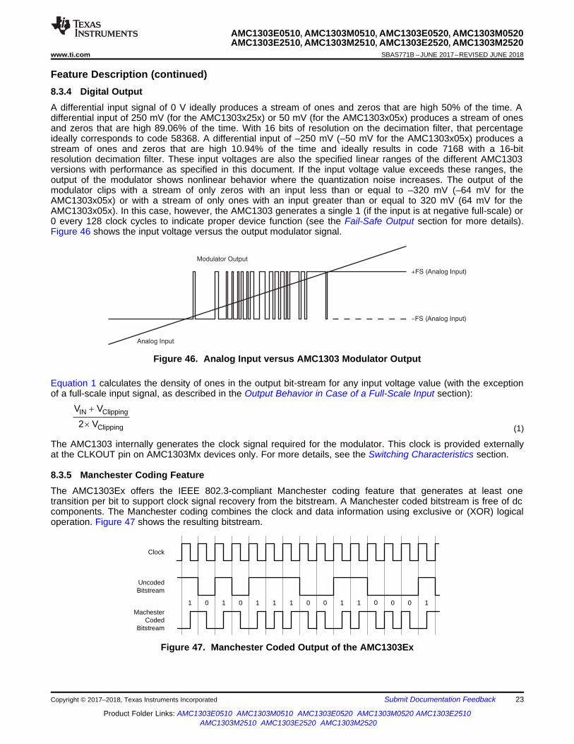
Feature Description (continued)8.3.4 Digital OutputA differential input signal of 0 V ideally produces a stream of ones and zeros that are high 50% of the time. Adifferential input of 250 mV (for the AMC1303x25x) or 50 mV (for the AMC1303x05x) produces a stream of onesand zeros that are high 89.06% of the time. With 16 bits of resolution on the decimation filter, that percentageideally corresponds to code 58368. A differential input of –250 mV (–50 mV for the AMC1303x05x) produces astream of ones and zeros that are high 10.94% of the time and ideally results in code 7168 with a 16-bitresolution decimation filter. These input voltages are also the specified linear ranges of the different AMC1303versions with performance as specified in this document. If the input voltage value exceeds these ranges, theoutput of the modulator shows nonlinear behavior where the quantization noise increases. The output of themodulator clips with a stream of only zeros with an input less than or equal to –320 mV (–64 mV for theAMC1303x05x) or with a stream of only ones with an input greater than or equal to 320 mV (64 mV for theAMC1303x05x). In this case, however, the AMC1303 generates a single 1 (if the input is at negative full-scale) or0 every 128 clock cycles to indicate proper device function (see the Fail-Safe Output section for more details).Figure 46 shows the input voltage versus the output modulator signal.
Figure 46. Analog Input versus AMC1303 Modulator Output
Equation 1 calculates the density of ones in the output bit-stream for any input voltage value (with the exceptionof a full-scale input signal, as described in the Output Behavior in Case of a Full-Scale Input section):
(1)
The AMC1303 internally generates the clock signal required for the modulator. This clock is provided externallyat the CLKOUT pin on AMC1303Mx devices only. For more details, see the Switching Characteristics section.
8.3.5 Manchester Coding FeatureThe AMC1303Ex offers the IEEE 802.3-compliant Manchester coding feature that generates at least onetransition per bit to support clock signal recovery from the bitstream. A Manchester coded bitstream is free of dccomponents. The Manchester coding combines the clock and data information using exclusive or (XOR) logicaloperation. Figure 47 shows the resulting bitstream.
Figure 47. Manchester Coded Output of the AMC1303Ex

CLKOUT(AMC1303Mx only)
DOUT VIN ��-320 mV (AMC1303x05x: ��-64 mV)
DOUT VIN ��320 mV (AMC1303x05x: H 64 mV)
... ...
...
...
...
...
127 CLK cycles 127 CLK cycles
CLKOUT(AMC1303Mx only)
256 cycles
4 cycles
VCM
DOUT
VCM ���9CMov
µ1¶�
VCM < VCMov
Valid bitstream
VCM < VCMov
Valid bitstream
...
µ1¶�
4 cycles
24
AMC1303E0510, AMC1303M0510, AMC1303E0520, AMC1303M0520AMC1303E2510, AMC1303M2510, AMC1303E2520, AMC1303M2520SBAS771B –JUNE 2017–REVISED JUNE 2018 www.ti.com
Product Folder Links: AMC1303E0510 AMC1303M0510 AMC1303E0520 AMC1303M0520 AMC1303E2510AMC1303M2510 AMC1303E2520 AMC1303M2520
Submit Documentation Feedback Copyright © 2017–2018, Texas Instruments Incorporated
8.4 Device Functional Modes
8.4.1 Fail-Safe OutputIn the case of a missing high-side supply voltage AVDD, the output of the ΔΣ modulator is not defined and cancause a system malfunction. In systems with high safety requirements, this behavior is not acceptable.Therefore, as shown in Figure 2, the AMC1303 implements a fail-safe output function that pulls the DOUT andCLKOUT outputs (AMC1303Mx only) to a steady-state logic 1 in case of a missing AVDD.
Similarly, as also shown in Figure 48, if the common-mode voltage of the input reaches or exceeds the specifiedcommon-mode overvoltage detection level VCMov as defined in the Electrical Characteristics table, the AMC1303generates a steady-state bitstream of logic 1's at the DOUT output.
In both cases, the steady-state logic 1 occurs on the DOUT output with a delay of two clock cycles after theevent of either exceeded common-mode input voltage or missing AVDD. Another 256 clock cycles are requiredfor the CLKOUT pin of the AMC1303Mx to be held at logic 1.
Figure 48. Fail-Safe Output of the AMC1303
8.4.2 Output Behavior in Case of a Full-Scale InputIf a full-scale input signal is applied to the AMC1303 (that is, |VIN| ≥ |VClipping|), Figure 49 shows that the devicegenerates a single one or zero every 128 bits at DOUT, depending on the actual polarity of the signal beingsensed. In this way, differentiating between a missing AVDD and a full-scale input signal is possible on thesystem level.
Figure 49. Overrange Output of the AMC1303

OSR
EN
OB
(bi
ts)
1 10 100 10000
2
4
6
8
10
12
14
16
D040
sinc3
sinc2
sinc1
SNR 1.76dBENOB
6.05dB�
� �3OSR
1
1 zH z
1 z
�
�
§ ·� ¨ ¸¨ ¸�© ¹
25
AMC1303E0510, AMC1303M0510, AMC1303E0520, AMC1303M0520AMC1303E2510, AMC1303M2510, AMC1303E2520, AMC1303M2520
www.ti.com SBAS771B –JUNE 2017–REVISED JUNE 2018
Product Folder Links: AMC1303E0510 AMC1303M0510 AMC1303E0520 AMC1303M0520 AMC1303E2510AMC1303M2510 AMC1303E2520 AMC1303M2520
Submit Documentation FeedbackCopyright © 2017–2018, Texas Instruments Incorporated
9 Application and Implementation
NOTEInformation in the following applications sections is not part of the TI componentspecification, and TI does not warrant its accuracy or completeness. TI’s customers areresponsible for determining suitability of components for their purposes. Customers shouldvalidate and test their design implementation to confirm system functionality.
9.1 Application Information
9.1.1 Digital Filter UsageThe modulator generates a bit stream that is processed by a digital filter to obtain a digital word similar to aconversion result of a conventional analog-to-digital converter (ADC). A very simple filter, shown in Equation 2,built with minimal effort and hardware, is a sinc3-type filter:
(2)
This filter provides the best output performance at the lowest hardware size (count of digital gates) for a second-order modulator. All the characterization in this document is done with a sinc3 filter with an oversampling ratio(OSR) of 256 and an output word size of 16 bits.
The effective number of bits (ENOB) is often used to compare the performance of ADCs and ΔΣ modulators.shows the ENOB of the AMC1303 with different oversampling ratios. In this document, Equation 3 calculates thisnumber from the SNR:
(3)
Figure 50. Measured Effective Number of Bits versus Oversampling Ratio
An example code for implementing a sinc3 filter in an FPGA is discussed in application note Combining ADS1202with FPGA Digital Filter for Current Measurement in Motor Control Applications, available for download atwww.ti.com.

SD-D1
TMS320F28x7x
DC link
RSHUNT
SD-D2
SD-D3
SD-D4
L1
L3
L2RSHUNT
RSHUNT
DOUT
CLKOUT
DVDD
DGNDAGND
AINN
AINP
AVDD
AMC1303Mx3.3 V
Power Board
Motor
Control Board
3.3 V
DOUT
CLKOUT
DVDD
DGNDAGND
AINN
AINP
AVDD
AMC1303Mx3.3 V 3.3 V
DOUT
CLKOUT
DVDD
DGNDAGND
AINN
AINP
AVDD
AMC1303Mx3.3 V 3.3 V
DOUT
CLKOUT
DVDD
DGNDAGND
AINN
AINP
AVDD
AMC1303Mx3.3 V 3.3 V
SD-C1
SD-C2
SD-C3
SD-C4
26
AMC1303E0510, AMC1303M0510, AMC1303E0520, AMC1303M0520AMC1303E2510, AMC1303M2510, AMC1303E2520, AMC1303M2520SBAS771B –JUNE 2017–REVISED JUNE 2018 www.ti.com
Product Folder Links: AMC1303E0510 AMC1303M0510 AMC1303E0520 AMC1303M0520 AMC1303E2510AMC1303M2510 AMC1303E2520 AMC1303M2520
Submit Documentation Feedback Copyright © 2017–2018, Texas Instruments Incorporated
9.2 Typical Applications
9.2.1 Frequency Inverter ApplicationIsolated ΔΣ modulators are widely used in new-generation frequency inverter designs because of their high acand dc performance. Frequency inverters are critical parts of industrial motor drives, photovoltaic inverters (stringand central inverters), uninterruptible power supplies (UPS), and other industrial applications.
Figure 51 shows a simplified schematic of the AMC1303Mx in a typical frequency inverter application as used inindustrial motor drives with shunt resistors (RSHUNT) used for current sensing. Depending on the system design,either all three or only two motor phase currents are sensed.
Figure 51. Simplified Diagram of the AMC1303Mx in a Frequency Inverter Application
SD-D1
TMS320F28x7x
DC link
RSHUNT
SD-D2
SD-D3
SD-D4
L1
L3
L2RSHUNT
RSHUNT
DOUT
CLKOUT
DVDD
DGNDAGND
AINN
AINP
AVDD
AMC1303Ex3.3 V
Power Board
Motor
Control Board
3.3 V
DOUT
CLKOUT
DVDD
DGNDAGND
AINN
AINP
AVDD
AMC1303Ex3.3 V 3.3 V
DOUT
CLKOUT
DVDD
DGNDAGND
AINN
AINP
AVDD
AMC1303Ex3.3 V 3.3 V
DOUT
CLKOUT
DVDD
DGNDAGND
AINN
AINP
AVDD
AMC1303Ex3.3 V 3.3 V
27
AMC1303E0510, AMC1303M0510, AMC1303E0520, AMC1303M0520AMC1303E2510, AMC1303M2510, AMC1303E2520, AMC1303M2520
www.ti.com SBAS771B –JUNE 2017–REVISED JUNE 2018
Product Folder Links: AMC1303E0510 AMC1303M0510 AMC1303E0520 AMC1303M0520 AMC1303E2510AMC1303M2510 AMC1303E2520 AMC1303M2520
Submit Documentation FeedbackCopyright © 2017–2018, Texas Instruments Incorporated
Typical Applications (continued)Figure 52 shows how the Manchester coded bitstream output of the AMC1303Ex minimizes the wiring efforts ofthe connection between the power and the control board. This bitstream output also allows the clock to begenerated locally on the power board without the having to adjust the propagation delay time of each DOUTconnection to fulfill the setup and hold time requirements of the microcontroller.
Figure 52. Simplified Diagram of the AMC1303Ex in a Frequency Inverter Application
In both examples shown previously, an additional fourth AMC1303 is used to support isolated voltage sensing ofthe dc link. This high voltage is reduced using a resistive divider and is sensed by the device across a smallerresistor. The value of this resistor can degrade the performance of the measurement, as described in the IsolatedVoltage Sensing section.
9.2.1.1 Design RequirementsTable 1 lists the parameters for the typical application in the Frequency Inverter Application section.
Table 1. Design RequirementsPARAMETER VALUE
High-side supply voltage 3.3 V or 5 VLow-side supply voltage 3.3 V or 5 V
Voltage drop across the shunt for a linear responseAMC1303x25x: ±250 mV (maximum)AMC1303x05x: ±50 mV (maximum)
Settling Time (µs)
EN
OB
(B
its)
0 2 4 6 8 10 12 14 16 18 20 22 24 260
2
4
6
8
10
12
14
16
D035
sinc3
sinc2
sinc1
Settling Time (µs)
EN
OB
(B
its)
0 2 4 6 8 10 12 14 16 18 20 22 24 260
2
4
6
8
10
12
14
16
D035
sinc3
sinc2
sinc1
28
AMC1303E0510, AMC1303M0510, AMC1303E0520, AMC1303M0520AMC1303E2510, AMC1303M2510, AMC1303E2520, AMC1303M2520SBAS771B –JUNE 2017–REVISED JUNE 2018 www.ti.com
Product Folder Links: AMC1303E0510 AMC1303M0510 AMC1303E0520 AMC1303M0520 AMC1303E2510AMC1303M2510 AMC1303E2520 AMC1303M2520
Submit Documentation Feedback Copyright © 2017–2018, Texas Instruments Incorporated
9.2.1.2 Detailed Design ProcedureThe high-side power supply (AVDD) for the AMC1303 device is derived from the power supply of the upper gatedriver. Further details are provided in the Power Supply Recommendations section.
The floating ground reference (AGND) is derived from one of the ends of the shunt resistor that is connected tothe negative input of the AMC1303 (AINN). If a four-pin shunt is used, the inputs of the device are connected tothe inner leads and AGND is connected to one of the outer shunt leads.
Use Ohm's Law to calculate the voltage drop across the shunt resistor (VSHUNT) for the desired measuredcurrent: VSHUNT = I × RSHUNT.
Consider the following two restrictions to choose the proper value of the shunt resistor RSHUNT:• The voltage drop caused by the nominal current range must not exceed the recommended differential input
voltage range: VSHUNT ≤ ±250 mV• The voltage drop caused by the maximum allowed overcurrent must not exceed the input voltage that causes
a clipping output: |VSHUNT| ≤ |VClipping|
The typically recommended RC filter in front of a ΔΣ modulator to improve signal-to-noise performance of thesignal path is not required for the AMC1303. By design, the input bandwidth of the analog front-end of the deviceis limited as specified in the Electrical Characteristics table.
For modulator output bitstream filtering, a device from TI's TMS320F2807x family of low-cost microcontrollers(MCUs) or TMS320F2837x family of dual-core MCUs is recommended. These families support up to eightchannels of dedicated hardwired filter structures that significantly simplify system level design by offering twofiltering paths per channel: one providing high accuracy results for the control loop and one fast response pathfor overcurrent detection.
9.2.1.3 Application CurvesIn motor control applications, a very fast response time for overcurrent detection is required. The time for fullysettling the filter in case of a step-signal at the input of the modulator depends on its order; that is, a sinc3 filterrequires three data updates for full settling (with fDATA = fCLK / OSR). Therefore, for overcurrent protection, filtertypes other than sinc3 can be a better choice; an alternative is the sinc2 filter. Figure 53 and Figure 54 comparethe settling times of different filter orders.
The delay time of a sinc filter with a continuous signal is half of its settling time.
AMC1303xxx20
Figure 53. Measured Effective Number of Bits versusSettling Time
AMC1303xxx10
Figure 54. Measured Effective Number of Bits versusSettling Time
û��Modulator
VCM = 1.9 V
3.3 V or 5 V
High Voltage Potential
R1
R2
R3
R4 R5
R4' R5'
RIND
AVDD
AINP
AINN
AGND
R3'
AGND
200 N��
IIB
AMC1303x25x
Gtot GIN
R3E = E +
R
29
AMC1303E0510, AMC1303M0510, AMC1303E0520, AMC1303M0520AMC1303E2510, AMC1303M2510, AMC1303E2520, AMC1303M2520
www.ti.com SBAS771B –JUNE 2017–REVISED JUNE 2018
Product Folder Links: AMC1303E0510 AMC1303M0510 AMC1303E0520 AMC1303M0520 AMC1303E2510AMC1303M2510 AMC1303E2520 AMC1303M2520
Submit Documentation FeedbackCopyright © 2017–2018, Texas Instruments Incorporated
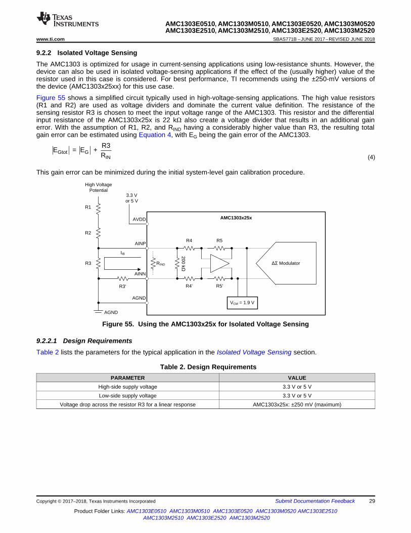
9.2.2 Isolated Voltage SensingThe AMC1303 is optimized for usage in current-sensing applications using low-resistance shunts. However, thedevice can also be used in isolated voltage-sensing applications if the effect of the (usually higher) value of theresistor used in this case is considered. For best performance, TI recommends using the ±250-mV versions ofthe device (AMC1303x25xx) for this use case.
Figure 55 shows a simplified circuit typically used in high-voltage-sensing applications. The high value resistors(R1 and R2) are used as voltage dividers and dominate the current value definition. The resistance of thesensing resistor R3 is chosen to meet the input voltage range of the AMC1303. This resistor and the differentialinput resistance of the AMC1303x25x is 22 kΩ also create a voltage divider that results in an additional gainerror. With the assumption of R1, R2, and RIND having a considerably higher value than R3, the resulting totalgain error can be estimated using Equation 4, with EG being the gain error of the AMC1303.
(4)
This gain error can be minimized during the initial system-level gain calibration procedure.
Figure 55. Using the AMC1303x25x for Isolated Voltage Sensing
9.2.2.1 Design RequirementsTable 2 lists the parameters for the typical application in the Isolated Voltage Sensing section.
Table 2. Design RequirementsPARAMETER VALUE
High-side supply voltage 3.3 V or 5 VLow-side supply voltage 3.3 V or 5 V
Voltage drop across the resistor R3 for a linear response AMC1303x25x: ±250 mV (maximum)
VCM (V)
I IB (P
A)
-0.5 0 0.5 1 1.5 2 2.5 3 3.5-80
-60
-40
-20
0
20
40
60
D005
AMC1306x25AMC1306x05
GR4
E (%) 1 100%R4' R3'
§ · � u¨ ¸�© ¹
30
AMC1303E0510, AMC1303M0510, AMC1303E0520, AMC1303M0520AMC1303E2510, AMC1303M2510, AMC1303E2520, AMC1303M2520SBAS771B –JUNE 2017–REVISED JUNE 2018 www.ti.com
Product Folder Links: AMC1303E0510 AMC1303M0510 AMC1303E0520 AMC1303M0520 AMC1303E2510AMC1303M2510 AMC1303E2520 AMC1303M2520
Submit Documentation Feedback Copyright © 2017–2018, Texas Instruments Incorporated
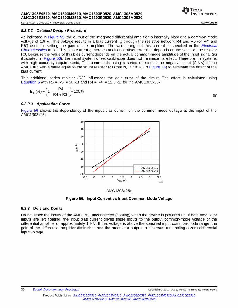
9.2.2.2 Detailed Design ProcedureAs indicated in Figure 55, the output of the integrated differential amplifier is internally biased to a common-modevoltage of 1.9 V. This voltage results in a bias current IIB through the resistive network R4 and R5 (or R4' andR5') used for setting the gain of the amplifier. The value range of this current is specified in the ElectricalCharacteristics table. This bias current generates additional offset error that depends on the value of the resistorR3. Because the value of this bias current depends on the actual common-mode amplitude of the input signal (asillustrated in Figure 56), the initial system offset calibration does not minimize its effect. Therefore, in systemswith high accuracy requirements, TI recommends using a series resistor at the negative input (AINN) of theAMC1303 with a value equal to the shunt resistor R3 (that is, R3' = R3 in Figure 55) to eliminate the effect of thebias current.
This additional series resistor (R3') influences the gain error of the circuit. The effect is calculated usingEquation 5 with R5 = R5' = 50 kΩ and R4 = R4' = 12.5 kΩ for the AMC1303x25x.
(5)
9.2.2.3 Application CurveFigure 56 shows the dependency of the input bias current on the common-mode voltage at the input of theAMC1303x25x.
AMC1303x25x
Figure 56. Input Current vs Input Common-Mode Voltage
9.2.3 Do's and Don'tsDo not leave the inputs of the AMC1303 unconnected (floating) when the device is powered up. If both modulatorinputs are left floating, the input bias current drives these inputs to the output common-mode voltage of thedifferential amplifier of approximately 1.9 V. If that voltage is above the specified input common-mode range, thegain of the differential amplifier diminishes and the modulator outputs a bitstream resembling a zero differentialinput voltage.

DVDD
DGNDAGND
AINP
AINN
AVDD
AMC1303Mx
HV+
HV-
To Load
FloatingPower Supply
20 V
3.0 V, or 3.3 V or 5.0 V
RSHUNT
5.1 V
R1800 �
Z11N751A
C12.2 �F
C20.1 �F
C40.1 �F
C52.2 �F
Gate Driver
Gate Driver
Rei
nfor
ced
Isol
atio
nDOUT
CLKOUT SD-Cx
SD-Dx
TMS320F2837x
Note: no CLKOUT connection using AMC1303Ex, pin 7 to be connected to DGND in this case
31
AMC1303E0510, AMC1303M0510, AMC1303E0520, AMC1303M0520AMC1303E2510, AMC1303M2510, AMC1303E2520, AMC1303M2520
www.ti.com SBAS771B –JUNE 2017–REVISED JUNE 2018
Product Folder Links: AMC1303E0510 AMC1303M0510 AMC1303E0520 AMC1303M0520 AMC1303E2510AMC1303M2510 AMC1303E2520 AMC1303M2520
Submit Documentation FeedbackCopyright © 2017–2018, Texas Instruments Incorporated
10 Power Supply RecommendationsIn a typical frequency-inverter application, the high-side power supply (AVDD) for the device is directly derivedfrom the floating power supply of the upper gate driver. For lowest system-level cost, a Zener diode can be usedto limit the voltage to 5 V or 3.3 V (±10%). Alternatively a low-cost low-drop regulator (LDO), for example theLM317-N, can be used to adjust the supply voltage level and minimize noise on the power supply node. A low-ESR decoupling capacitor of 0.1 µF is recommended for filtering this power-supply path. Place this capacitor (C2in Figure 57) as close as possible to the AVDD pin of the AMC1303 for best performance. Further, an additionalcapacitor with a value in the range of 2.2 µF to 10 µF is recommended.
The floating ground reference (AGND) is derived from the end of the shunt resistor, which is connected to thenegative input (AINN) of the device. If a four-pin shunt is used, the device inputs are connected to the inner leadsand AGND is connected to one of the outer leads of the shunt.
For decoupling of the digital power supply on the controller side, TI recommends using a 0.1-µF capacitorassembled as close to the DVDD pin of the AMC1303 as possible, followed by an additional capacitor in therange of 2.2 µF to 10 µF.
Figure 57. Decoupling the AMC1303

To Digital Filter(MCU)
Clearance area,to be kept free of any conductive materials.
AMC1303Mx
AINP
AINN DOUT
DGND
1 16
CLKOUT
DVDD
0.1 µF
SMD0603
AGND
LEGEND
Copper Pour and Traces
High-Side Area
Controller-Side Area
Via to Ground Plane
Via to Supply Plane
To Floating Power Supply
2.2 µF
SMD0603
Shu
nt R
esis
tor
AVDD
0.1 µF
SMD0603
2.2 µF
SMD0603
CFLT
SMD0603
RFLTSMD0603
RFLTSMD0603
Note: no CLKOUT connection using AMC1303Ex, pin 7 to be connected to DGND in this case
32
AMC1303E0510, AMC1303M0510, AMC1303E0520, AMC1303M0520AMC1303E2510, AMC1303M2510, AMC1303E2520, AMC1303M2520SBAS771B –JUNE 2017–REVISED JUNE 2018 www.ti.com
Product Folder Links: AMC1303E0510 AMC1303M0510 AMC1303E0520 AMC1303M0520 AMC1303E2510AMC1303M2510 AMC1303E2520 AMC1303M2520
Submit Documentation Feedback Copyright © 2017–2018, Texas Instruments Incorporated
11 Layout
11.1 Layout GuidelinesFigure 58 shows a layout recommendation detailing the critical placement of the decoupling capacitors (as closeas possible to the AMC1303) and placement of the other components required by the device. For bestperformance, place the shunt resistor and the antialiasing filter components as close as possible to the AINP andAINN inputs of the AMC1303 and keep the layout of both connections symmetrical.
11.2 Layout Example
Figure 58. Recommended Layout of the AMC1303
33
AMC1303E0510, AMC1303M0510, AMC1303E0520, AMC1303M0520AMC1303E2510, AMC1303M2510, AMC1303E2520, AMC1303M2520
www.ti.com SBAS771B –JUNE 2017–REVISED JUNE 2018
Product Folder Links: AMC1303E0510 AMC1303M0510 AMC1303E0520 AMC1303M0520 AMC1303E2510AMC1303M2510 AMC1303E2520 AMC1303M2520
Submit Documentation FeedbackCopyright © 2017–2018, Texas Instruments Incorporated
12 Device and Documentation Support
12.1 Device Support
12.1.1 Device Nomenclature
12.1.1.1 Isolation GlossarySee the Isolation Glossary
12.2 Documentation Support
12.2.1 Related Documentation• AMC1210 Quad Digital Filter for 2nd-Order Delta-Sigma Modulator• MSP430F677x Polyphase Metering SoCs• TMS320F2807x Piccolo™ Microcontrollers• TMS320F2837xD Dual-Core Delfino™ Microcontrollers• ISO72x Digital Isolator Magnetic-Field Immunity• Combining ADS1202 with FPGA Digital Filter for Current Measurement in Motor Control Applications
12.3 Related LinksThe table below lists quick access links. Categories include technical documents, support and communityresources, tools and software, and quick access to order now.
Table 3. Related Links
PARTS PRODUCT FOLDER ORDER NOW TECHNICALDOCUMENTS
TOOLS &SOFTWARE
SUPPORT &COMMUNITY
AMC1303E0510 Click here Click here Click here Click here Click hereAMC1303M0510 Click here Click here Click here Click here Click hereAMC1303E0520 Click here Click here Click here Click here Click hereAMC1303M0520 Click here Click here Click here Click here Click hereAMC1303E2510 Click here Click here Click here Click here Click hereAMC1303M2510 Click here Click here Click here Click here Click hereAMC1303E2520 Click here Click here Click here Click here Click hereAMC1303M2520 Click here Click here Click here Click here Click here
12.4 Receiving Notification of Documentation UpdatesTo receive notification of documentation updates, navigate to the device product folder on ti.com. In the upperright corner, click on Alert me to register and receive a weekly digest of any product information that haschanged. For change details, review the revision history included in any revised document.
12.5 Community ResourcesThe following links connect to TI community resources. Linked contents are provided "AS IS" by the respectivecontributors. They do not constitute TI specifications and do not necessarily reflect TI's views; see TI's Terms ofUse.
TI E2E™ Online Community TI's Engineer-to-Engineer (E2E) Community. Created to foster collaborationamong engineers. At e2e.ti.com, you can ask questions, share knowledge, explore ideas and helpsolve problems with fellow engineers.
Design Support TI's Design Support Quickly find helpful E2E forums along with design support tools andcontact information for technical support.

34
AMC1303E0510, AMC1303M0510, AMC1303E0520, AMC1303M0520AMC1303E2510, AMC1303M2510, AMC1303E2520, AMC1303M2520SBAS771B –JUNE 2017–REVISED JUNE 2018 www.ti.com
Product Folder Links: AMC1303E0510 AMC1303M0510 AMC1303E0520 AMC1303M0520 AMC1303E2510AMC1303M2510 AMC1303E2520 AMC1303M2520
Submit Documentation Feedback Copyright © 2017–2018, Texas Instruments Incorporated
12.6 TrademarksE2E is a trademark of Texas Instruments.All other trademarks are the property of their respective owners.
12.7 Electrostatic Discharge CautionThis integrated circuit can be damaged by ESD. Texas Instruments recommends that all integrated circuits be handled withappropriate precautions. Failure to observe proper handling and installation procedures can cause damage.
ESD damage can range from subtle performance degradation to complete device failure. Precision integrated circuits may be moresusceptible to damage because very small parametric changes could cause the device not to meet its published specifications.
12.8 GlossarySLYZ022 — TI Glossary.
This glossary lists and explains terms, acronyms, and definitions.
13 Mechanical, Packaging, and Orderable InformationThe following pages include mechanical, packaging, and orderable information. This information is the mostcurrent data available for the designated devices. This data is subject to change without notice and revision ofthis document. For browser-based versions of this data sheet, refer to the left-hand navigation.

PACKAGE OPTION ADDENDUM
www.ti.com 14-Jun-2018
Addendum-Page 1
PACKAGING INFORMATION
Orderable Device Status(1)
Package Type PackageDrawing
Pins PackageQty
Eco Plan(2)
Lead/Ball Finish(6)
MSL Peak Temp(3)
Op Temp (°C) Device Marking(4/5)
Samples
AMC1303E0510DWV ACTIVE SOIC DWV 8 64 Green (RoHS& no Sb/Br)
CU NIPDAU Level-3-260C-168 HR -40 to 125 1303E051
AMC1303E0510DWVR ACTIVE SOIC DWV 8 1000 Green (RoHS& no Sb/Br)
CU NIPDAU Level-3-260C-168 HR -40 to 125 1303E051
AMC1303E0520DWV ACTIVE SOIC DWV 8 64 Green (RoHS& no Sb/Br)
CU NIPDAU Level-3-260C-168 HR -40 to 125 1303E052
AMC1303E0520DWVR ACTIVE SOIC DWV 8 1000 Green (RoHS& no Sb/Br)
CU NIPDAU Level-3-260C-168 HR -40 to 125 1303E052
AMC1303E2510DWV ACTIVE SOIC DWV 8 64 Green (RoHS& no Sb/Br)
CU NIPDAU Level-3-260C-168 HR -40 to 125 1303E251
AMC1303E2510DWVR ACTIVE SOIC DWV 8 1000 Green (RoHS& no Sb/Br)
CU NIPDAU Level-3-260C-168 HR -40 to 125 1303E251
AMC1303E2520DWV ACTIVE SOIC DWV 8 64 Green (RoHS& no Sb/Br)
CU NIPDAU Level-3-260C-168 HR -40 to 125 1303E252
AMC1303E2520DWVR ACTIVE SOIC DWV 8 1000 Green (RoHS& no Sb/Br)
CU NIPDAU Level-3-260C-168 HR -40 to 125 1303E252
AMC1303M0510DWV ACTIVE SOIC DWV 8 64 Green (RoHS& no Sb/Br)
CU NIPDAU Level-3-260C-168 HR -40 to 125 1303M051
AMC1303M0510DWVR ACTIVE SOIC DWV 8 1000 Green (RoHS& no Sb/Br)
CU NIPDAU Level-3-260C-168 HR -40 to 125 1303M051
AMC1303M0520DWV ACTIVE SOIC DWV 8 64 Green (RoHS& no Sb/Br)
CU NIPDAU Level-3-260C-168 HR -40 to 125 1303M052
AMC1303M0520DWVR ACTIVE SOIC DWV 8 1000 Green (RoHS& no Sb/Br)
CU NIPDAU Level-3-260C-168 HR -40 to 125 1303M052
AMC1303M2510DWV ACTIVE SOIC DWV 8 64 Green (RoHS& no Sb/Br)
CU NIPDAU Level-3-260C-168 HR -40 to 125 1303M251
AMC1303M2510DWVR ACTIVE SOIC DWV 8 1000 Green (RoHS& no Sb/Br)
CU NIPDAU Level-3-260C-168 HR -40 to 125 1303M251
AMC1303M2520DWV ACTIVE SOIC DWV 8 64 Green (RoHS& no Sb/Br)
CU NIPDAU Level-3-260C-168 HR -40 to 125 1303M252
AMC1303M2520DWVR ACTIVE SOIC DWV 8 1000 Green (RoHS& no Sb/Br)
CU NIPDAU Level-3-260C-168 HR -40 to 125 1303M252
(1) The marketing status values are defined as follows:ACTIVE: Product device recommended for new designs.
PACKAGE OPTION ADDENDUM
www.ti.com 14-Jun-2018
Addendum-Page 2
LIFEBUY: TI has announced that the device will be discontinued, and a lifetime-buy period is in effect.NRND: Not recommended for new designs. Device is in production to support existing customers, but TI does not recommend using this part in a new design.PREVIEW: Device has been announced but is not in production. Samples may or may not be available.OBSOLETE: TI has discontinued the production of the device.
(2) RoHS: TI defines "RoHS" to mean semiconductor products that are compliant with the current EU RoHS requirements for all 10 RoHS substances, including the requirement that RoHS substancedo not exceed 0.1% by weight in homogeneous materials. Where designed to be soldered at high temperatures, "RoHS" products are suitable for use in specified lead-free processes. TI mayreference these types of products as "Pb-Free".RoHS Exempt: TI defines "RoHS Exempt" to mean products that contain lead but are compliant with EU RoHS pursuant to a specific EU RoHS exemption.Green: TI defines "Green" to mean the content of Chlorine (Cl) and Bromine (Br) based flame retardants meet JS709B low halogen requirements of <=1000ppm threshold. Antimony trioxide basedflame retardants must also meet the <=1000ppm threshold requirement.
(3) MSL, Peak Temp. - The Moisture Sensitivity Level rating according to the JEDEC industry standard classifications, and peak solder temperature.
(4) There may be additional marking, which relates to the logo, the lot trace code information, or the environmental category on the device.
(5) Multiple Device Markings will be inside parentheses. Only one Device Marking contained in parentheses and separated by a "~" will appear on a device. If a line is indented then it is a continuationof the previous line and the two combined represent the entire Device Marking for that device.
(6) Lead/Ball Finish - Orderable Devices may have multiple material finish options. Finish options are separated by a vertical ruled line. Lead/Ball Finish values may wrap to two lines if the finishvalue exceeds the maximum column width.
Important Information and Disclaimer:The information provided on this page represents TI's knowledge and belief as of the date that it is provided. TI bases its knowledge and belief on informationprovided by third parties, and makes no representation or warranty as to the accuracy of such information. Efforts are underway to better integrate information from third parties. TI has taken andcontinues to take reasonable steps to provide representative and accurate information but may not have conducted destructive testing or chemical analysis on incoming materials and chemicals.TI and TI suppliers consider certain information to be proprietary, and thus CAS numbers and other limited information may not be available for release.
In no event shall TI's liability arising out of such information exceed the total purchase price of the TI part(s) at issue in this document sold by TI to Customer on an annual basis.

TAPE AND REEL INFORMATION
*All dimensions are nominal
Device PackageType
PackageDrawing
Pins SPQ ReelDiameter
(mm)
ReelWidth
W1 (mm)
A0(mm)
B0(mm)
K0(mm)
P1(mm)
W(mm)
Pin1Quadrant
AMC1303E0510DWVR SOIC DWV 8 1000 330.0 16.4 12.05 6.15 3.3 16.0 16.0 Q1
AMC1303E0520DWVR SOIC DWV 8 1000 330.0 16.4 12.05 6.15 3.3 16.0 16.0 Q1
AMC1303E2510DWVR SOIC DWV 8 1000 330.0 16.4 12.05 6.15 3.3 16.0 16.0 Q1
AMC1303E2520DWVR SOIC DWV 8 1000 330.0 16.4 12.05 6.15 3.3 16.0 16.0 Q1
AMC1303M0510DWVR SOIC DWV 8 1000 330.0 16.4 12.05 6.15 3.3 16.0 16.0 Q1
AMC1303M0520DWVR SOIC DWV 8 1000 330.0 16.4 12.05 6.15 3.3 16.0 16.0 Q1
AMC1303M2510DWVR SOIC DWV 8 1000 330.0 16.4 12.05 6.15 3.3 16.0 16.0 Q1
AMC1303M2520DWVR SOIC DWV 8 1000 330.0 16.4 12.05 6.15 3.3 16.0 16.0 Q1
PACKAGE MATERIALS INFORMATION
www.ti.com 15-Jun-2018
Pack Materials-Page 1

*All dimensions are nominal
Device Package Type Package Drawing Pins SPQ Length (mm) Width (mm) Height (mm)
AMC1303E0510DWVR SOIC DWV 8 1000 367.0 367.0 38.0
AMC1303E0520DWVR SOIC DWV 8 1000 367.0 367.0 38.0
AMC1303E2510DWVR SOIC DWV 8 1000 367.0 367.0 38.0
AMC1303E2520DWVR SOIC DWV 8 1000 367.0 367.0 38.0
AMC1303M0510DWVR SOIC DWV 8 1000 367.0 367.0 38.0
AMC1303M0520DWVR SOIC DWV 8 1000 367.0 367.0 38.0
AMC1303M2510DWVR SOIC DWV 8 1000 367.0 367.0 38.0
AMC1303M2520DWVR SOIC DWV 8 1000 367.0 367.0 38.0
PACKAGE MATERIALS INFORMATION
www.ti.com 15-Jun-2018
Pack Materials-Page 2

www.ti.com
PACKAGE OUTLINE
C
TYP11.5 0.25
2.8 MAX
TYP0.330.13
0 -8
6X 1.27
8X 0.510.31
2X3.81
0.460.36
1.00.5
0.25GAGE PLANE
A
NOTE 3
5.955.75
BNOTE 4
7.67.4
(2.286)
(2)
4218796/A 09/2013
SOIC - 2.8 mm max heightDWV0008ASOIC
NOTES: 1. All linear dimensions are in millimeters. Dimensions in parenthesis are for reference only. Dimensioning and tolerancing per ASME Y14.5M. 2. This drawing is subject to change without notice. 3. This dimension does not include mold flash, protrusions, or gate burrs. Mold flash, protrusions, or gate burrs shall not exceed 0.15 mm, per side. 4. This dimension does not include interlead flash. Interlead flash shall not exceed 0.25 mm, per side.
18
0.25 C A B
54
AREAPIN 1 ID
SEATING PLANE
0.1 C
SEE DETAIL A
DETAIL ATYPICAL
SCALE 2.000

www.ti.com
EXAMPLE BOARD LAYOUT
(10.9)
0.07 MAXALL AROUND
0.07 MINALL AROUND
8X (1.8)
8X (0.6)
6X (1.27)
4218796/A 09/2013
SOIC - 2.8 mm max heightDWV0008ASOIC
SYMM
SYMM
SEE DETAILS
LAND PATTERN EXAMPLE9.1 mm NOMINAL CLEARANCE/CREEPAGE
SCALE:6X
NOTES: (continued) 5. Publication IPC-7351 may have alternate designs. 6. Solder mask tolerances between and around signal pads can vary based on board fabrication site.
METAL SOLDER MASKOPENING
NON SOLDER MASKDEFINED
SOLDER MASK DETAILS
OPENINGSOLDER MASK METAL
SOLDER MASKDEFINED

www.ti.com
EXAMPLE STENCIL DESIGN
8X (1.8)
8X (0.6)
6X (1.27)
(10.9)
4218796/A 09/2013
SOIC - 2.8 mm max heightDWV0008ASOIC
NOTES: (continued) 7. Laser cutting apertures with trapezoidal walls and rounded corners may offer better paste release. IPC-7525 may have alternate design recommendations. 8. Board assembly site may have different recommendations for stencil design.
SOLDER PASTE EXAMPLEBASED ON 0.125 mm THICK STENCIL
SCALE:6X
SYMM
SYMM

IMPORTANT NOTICE
Texas Instruments Incorporated (TI) reserves the right to make corrections, enhancements, improvements and other changes to itssemiconductor products and services per JESD46, latest issue, and to discontinue any product or service per JESD48, latest issue. Buyersshould obtain the latest relevant information before placing orders and should verify that such information is current and complete.TI’s published terms of sale for semiconductor products (http://www.ti.com/sc/docs/stdterms.htm) apply to the sale of packaged integratedcircuit products that TI has qualified and released to market. Additional terms may apply to the use or sale of other types of TI products andservices.Reproduction of significant portions of TI information in TI data sheets is permissible only if reproduction is without alteration and isaccompanied by all associated warranties, conditions, limitations, and notices. TI is not responsible or liable for such reproduceddocumentation. Information of third parties may be subject to additional restrictions. Resale of TI products or services with statementsdifferent from or beyond the parameters stated by TI for that product or service voids all express and any implied warranties for theassociated TI product or service and is an unfair and deceptive business practice. TI is not responsible or liable for any such statements.Buyers and others who are developing systems that incorporate TI products (collectively, “Designers”) understand and agree that Designersremain responsible for using their independent analysis, evaluation and judgment in designing their applications and that Designers havefull and exclusive responsibility to assure the safety of Designers' applications and compliance of their applications (and of all TI productsused in or for Designers’ applications) with all applicable regulations, laws and other applicable requirements. Designer represents that, withrespect to their applications, Designer has all the necessary expertise to create and implement safeguards that (1) anticipate dangerousconsequences of failures, (2) monitor failures and their consequences, and (3) lessen the likelihood of failures that might cause harm andtake appropriate actions. Designer agrees that prior to using or distributing any applications that include TI products, Designer willthoroughly test such applications and the functionality of such TI products as used in such applications.TI’s provision of technical, application or other design advice, quality characterization, reliability data or other services or information,including, but not limited to, reference designs and materials relating to evaluation modules, (collectively, “TI Resources”) are intended toassist designers who are developing applications that incorporate TI products; by downloading, accessing or using TI Resources in anyway, Designer (individually or, if Designer is acting on behalf of a company, Designer’s company) agrees to use any particular TI Resourcesolely for this purpose and subject to the terms of this Notice.TI’s provision of TI Resources does not expand or otherwise alter TI’s applicable published warranties or warranty disclaimers for TIproducts, and no additional obligations or liabilities arise from TI providing such TI Resources. TI reserves the right to make corrections,enhancements, improvements and other changes to its TI Resources. TI has not conducted any testing other than that specificallydescribed in the published documentation for a particular TI Resource.Designer is authorized to use, copy and modify any individual TI Resource only in connection with the development of applications thatinclude the TI product(s) identified in such TI Resource. NO OTHER LICENSE, EXPRESS OR IMPLIED, BY ESTOPPEL OR OTHERWISETO ANY OTHER TI INTELLECTUAL PROPERTY RIGHT, AND NO LICENSE TO ANY TECHNOLOGY OR INTELLECTUAL PROPERTYRIGHT OF TI OR ANY THIRD PARTY IS GRANTED HEREIN, including but not limited to any patent right, copyright, mask work right, orother intellectual property right relating to any combination, machine, or process in which TI products or services are used. Informationregarding or referencing third-party products or services does not constitute a license to use such products or services, or a warranty orendorsement thereof. Use of TI Resources may require a license from a third party under the patents or other intellectual property of thethird party, or a license from TI under the patents or other intellectual property of TI.TI RESOURCES ARE PROVIDED “AS IS” AND WITH ALL FAULTS. TI DISCLAIMS ALL OTHER WARRANTIES ORREPRESENTATIONS, EXPRESS OR IMPLIED, REGARDING RESOURCES OR USE THEREOF, INCLUDING BUT NOT LIMITED TOACCURACY OR COMPLETENESS, TITLE, ANY EPIDEMIC FAILURE WARRANTY AND ANY IMPLIED WARRANTIES OFMERCHANTABILITY, FITNESS FOR A PARTICULAR PURPOSE, AND NON-INFRINGEMENT OF ANY THIRD PARTY INTELLECTUALPROPERTY RIGHTS. TI SHALL NOT BE LIABLE FOR AND SHALL NOT DEFEND OR INDEMNIFY DESIGNER AGAINST ANY CLAIM,INCLUDING BUT NOT LIMITED TO ANY INFRINGEMENT CLAIM THAT RELATES TO OR IS BASED ON ANY COMBINATION OFPRODUCTS EVEN IF DESCRIBED IN TI RESOURCES OR OTHERWISE. IN NO EVENT SHALL TI BE LIABLE FOR ANY ACTUAL,DIRECT, SPECIAL, COLLATERAL, INDIRECT, PUNITIVE, INCIDENTAL, CONSEQUENTIAL OR EXEMPLARY DAMAGES INCONNECTION WITH OR ARISING OUT OF TI RESOURCES OR USE THEREOF, AND REGARDLESS OF WHETHER TI HAS BEENADVISED OF THE POSSIBILITY OF SUCH DAMAGES.Unless TI has explicitly designated an individual product as meeting the requirements of a particular industry standard (e.g., ISO/TS 16949and ISO 26262), TI is not responsible for any failure to meet such industry standard requirements.Where TI specifically promotes products as facilitating functional safety or as compliant with industry functional safety standards, suchproducts are intended to help enable customers to design and create their own applications that meet applicable functional safety standardsand requirements. Using products in an application does not by itself establish any safety features in the application. Designers mustensure compliance with safety-related requirements and standards applicable to their applications. Designer may not use any TI products inlife-critical medical equipment unless authorized officers of the parties have executed a special contract specifically governing such use.Life-critical medical equipment is medical equipment where failure of such equipment would cause serious bodily injury or death (e.g., lifesupport, pacemakers, defibrillators, heart pumps, neurostimulators, and implantables). Such equipment includes, without limitation, allmedical devices identified by the U.S. Food and Drug Administration as Class III devices and equivalent classifications outside the U.S.TI may expressly designate certain products as completing a particular qualification (e.g., Q100, Military Grade, or Enhanced Product).Designers agree that it has the necessary expertise to select the product with the appropriate qualification designation for their applicationsand that proper product selection is at Designers’ own risk. Designers are solely responsible for compliance with all legal and regulatoryrequirements in connection with such selection.Designer will fully indemnify TI and its representatives against any damages, costs, losses, and/or liabilities arising out of Designer’s non-compliance with the terms and provisions of this Notice.
Mailing Address: Texas Instruments, Post Office Box 655303, Dallas, Texas 75265Copyright © 2018, Texas Instruments Incorporated