Embed Size (px)
Citation preview

AMD SB700/710/750 BIOS Developer’s Guide
Technical Reference Manual Rev. 1.00
PN: 43366_sb7xx_bdg_pub_1.00
© 2009 Advanced Micro Devices, Inc.
Trademarks AMD, the AMD Arrow logo, Athlon, and combinations thereof, ATI, ATI logo, Radeon, and CrossFire are trademarks of Advanced Micro Devices, Inc.
HyperTransport is a licensed trademark of the HyperTransport Technology Consortium.
Microsoft and Windows are registered trademarks of Microsoft Corporation.
Other product names used in this publication are for identification purposes only and may be trademarks of their respective companies.
Disclaimer
The contents of this document are provided in connection with Advanced Micro Devices, Inc. ("AMD") products. AMD makes no representations or warranties with respect to the accuracy or completeness of the contents of this publication and reserves the right to make changes to specifications and product descriptions at any time without notice. No license, whether express, implied, arising by estoppel, or otherwise, to any intellectual property rights are granted by this publication. Except as set forth in AMD's Standard Terms and Conditions of Sale, AMD assumes no liability whatsoever, and disclaims any express or implied warranty, relating to its products including, but not limited to, the implied warranty of merchantability, fitness for a particular purpose, or infringement of any intellectual property right.
AMD's products are not designed, intended, authorized or warranted for use as components in systems intended for surgical implant into the body, or in other applications intended to support or sustain life, or in any other application in which the failure of AMD's product could create a situation where personal injury, death, or severe property or environmental damage may occur. AMD reserves the right to discontinue or make changes to its products at any time without notice.
.
©2009 Advanced Micro Devices, Inc. Table of Contents
AMD SB700 BIOS Developer’s Guide AMD Confidential Page 3
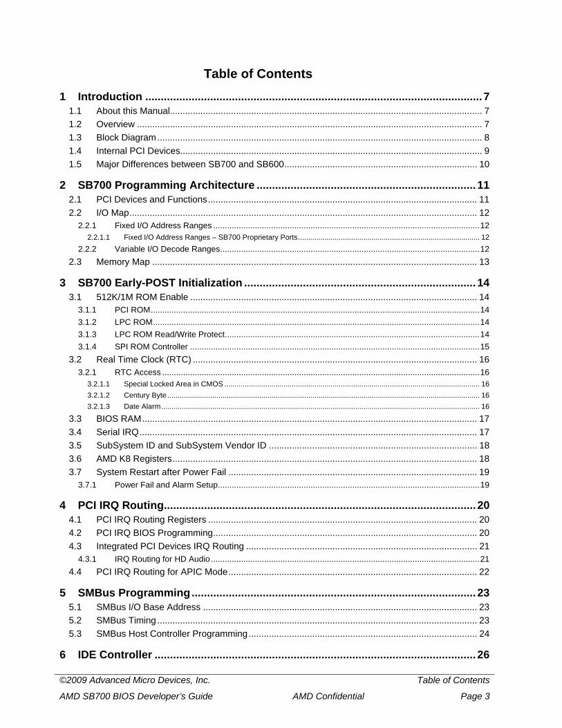
Table of Contents 1 Introduction ............................................................................................................. 7
1.1 About this Manual........................................................................................................................... 7 1.2 Overview ........................................................................................................................................ 7 1.3 Block Diagram................................................................................................................................ 8 1.4 Internal PCI Devices....................................................................................................................... 9 1.5 Major Differences between SB700 and SB600............................................................................ 10
2 SB700 Programming Architecture ....................................................................... 11 2.1 PCI Devices and Functions.......................................................................................................... 11 2.2 I/O Map......................................................................................................................................... 12
2.2.1 Fixed I/O Address Ranges ...................................................................................................................12 2.2.1.1 Fixed I/O Address Ranges – SB700 Proprietary Ports......................................................................................... 12
2.2.2 Variable I/O Decode Ranges................................................................................................................12 2.3 Memory Map ................................................................................................................................ 13
3 SB700 Early-POST Initialization ........................................................................... 14 3.1 512K/1M ROM Enable ................................................................................................................. 14
3.1.1 PCI ROM..............................................................................................................................................14 3.1.2 LPC ROM.............................................................................................................................................14 3.1.3 LPC ROM Read/Write Protect..............................................................................................................14 3.1.4 SPI ROM Controller .............................................................................................................................15
3.2 Real Time Clock (RTC) ................................................................................................................ 16 3.2.1 RTC Access .........................................................................................................................................16
3.2.1.1 Special Locked Area in CMOS ............................................................................................................................. 16 3.2.1.2 Century Byte ......................................................................................................................................................... 16 3.2.1.3 Date Alarm............................................................................................................................................................ 16
3.3 BIOS RAM.................................................................................................................................... 17 3.4 Serial IRQ..................................................................................................................................... 17 3.5 SubSystem ID and SubSystem Vendor ID .................................................................................. 18 3.6 AMD K8 Registers........................................................................................................................ 18 3.7 System Restart after Power Fail .................................................................................................. 19
3.7.1 Power Fail and Alarm Setup.................................................................................................................19
4 PCI IRQ Routing..................................................................................................... 20 4.1 PCI IRQ Routing Registers .......................................................................................................... 20 4.2 PCI IRQ BIOS Programming........................................................................................................ 20 4.3 Integrated PCI Devices IRQ Routing ........................................................................................... 21
4.3.1 IRQ Routing for HD Audio....................................................................................................................21 4.4 PCI IRQ Routing for APIC Mode.................................................................................................. 22
5 SMBus Programming............................................................................................ 23 5.1 SMBus I/O Base Address ............................................................................................................ 23 5.2 SMBus Timing .............................................................................................................................. 23 5.3 SMBus Host Controller Programming.......................................................................................... 24
6 IDE Controller ........................................................................................................ 26
©2009 Advanced Micro Devices, Inc. Table of Contents
AMD SB700 BIOS Developer’s Guide AMD Confidential Page 4
6.1 IDE Channel Enable/Disable........................................................................................................ 26 6.1.1 IDE Channel Enable.............................................................................................................................26 6.1.2 IDE Channel Disable............................................................................................................................26
6.2 PIO Modes ................................................................................................................................... 27 6.2.1 PIO Mode.............................................................................................................................................27 6.2.2 PIO Timing ...........................................................................................................................................27
6.3 DMA Modes.................................................................................................................................. 27 6.3.1 Legacy (Multi-Words) DMA mode ........................................................................................................27 6.3.2 Ultra-DMA Mode ..................................................................................................................................28
7 USB Controllers..................................................................................................... 29 7.1 Interrupt Routing for USB Controllers .......................................................................................... 29
8 Serial ATA (SATA) ................................................................................................. 30 8.1 SATA New Features..................................................................................................................... 31 8.2 Device ID...................................................................................................................................... 33 8.3 SATA Controller Operating Modes............................................................................................... 34 8.4 SATA Hot Plug ............................................................................................................................. 34
8.4.1 Sample Code .......................................................................................................................................34
9 Power Management............................................................................................... 35 9.1 SMI Handling – EOS (PM IO Reg10h[Bit0]) ................................................................................ 35 9.2 Programmable I/Os ...................................................................................................................... 35 9.3 Power Management Timers ......................................................................................................... 36
9.3.1 PM Timer 1 (Inactivity Timer) ...............................................................................................................36 9.3.2 PM Timer 2 (Activity Timer)..................................................................................................................36
9.4 SMI Events ................................................................................................................................... 37 9.4.1 Power Button........................................................................................................................................38
9.5 C-State Break Events................................................................................................................... 38 9.5.1 Break Events for C2 State....................................................................................................................38 9.5.2 Break Events for C3 and C4 States .....................................................................................................38
9.6 Save/Restore Sequence for S3 State .......................................................................................... 38 9.6.1 Register Save Sequence for S3 State..................................................................................................38
9.7 Wake on Events ........................................................................................................................... 39 9.8 Sleep SMI Events......................................................................................................................... 39
9.8.1 Sleep SMI Control Register..................................................................................................................39 9.8.2 Sleep SMI Programming Sequence .....................................................................................................39
9.8.2.1 Set Sleep SMI Control Register............................................................................................................................ 39 9.8.2.2 Enter Sleep SMI# Routine .................................................................................................................................... 39
10 APIC Programming................................................................................................ 40 10.1 Northbridge APIC Enable............................................................................................................. 40 10.2 Southbridge APIC Enable ............................................................................................................ 40 10.3 IOAPIC Base Address.................................................................................................................. 40 10.4 APIC IRQ Assignment.................................................................................................................. 40 10.5 APIC IRQ Routing ........................................................................................................................ 41
11 Watchdog Timer .................................................................................................... 42
©2009 Advanced Micro Devices, Inc. Table of Contents
AMD SB700 BIOS Developer’s Guide AMD Confidential Page 5
12 A-Link Bridge......................................................................................................... 44 12.1 Programming Procedure .............................................................................................................. 45 12.2 A-Link Express Configuration DMA Access................................................................................. 46 12.3 Enable Non-Posted Memory Write for K8 Platform. .................................................................... 47
13 High Precision Event Timer (HPET) ..................................................................... 48 13.1 Initialization................................................................................................................................... 48
13.1.1 Sample Initialization Code....................................................................................................................48 13.2 ACPI HPET Description Table ..................................................................................................... 49 13.3 HPET Support for Vista................................................................................................................ 49
14 Sample Programs.................................................................................................. 50 14.1 IXP700 Register Initialization on Power-Up ................................................................................. 50
14.1.1 Initialization of PCI IRQ Routing before Resource Allocation...............................................................50 14.2 Setup Options............................................................................................................................... 51
14.2.1 64 Bytes DMA ......................................................................................................................................51 14.2.2 USB Overcurrent Detection Disable.....................................................................................................51 14.2.3 C3 Support ...........................................................................................................................................51 14.2.4 Subtractive Decoding for P2P Bridge...................................................................................................52 14.2.5 Enable/Disable On-Chip SATA ............................................................................................................53 14.2.6 Change Class ID for SATA...................................................................................................................53 14.2.7 Disable AC97 Audio or MC97 Modem .................................................................................................55 14.2.8 Enable EHCI Controller ........................................................................................................................56 14.2.9 Enable OHCI Controller .......................................................................................................................58
14.3 IDE Settings ................................................................................................................................. 58 14.3.1 PIO Mode Settings ...............................................................................................................................58 14.3.2 Multiword DMA Settings.......................................................................................................................60 14.3.3 UDMA Mode Settings...........................................................................................................................60 14.3.4 IDE Channel Disable............................................................................................................................61 14.3.5 IDE Channel Enable.............................................................................................................................63
14.4 USB Controller Reset at Hard Reset............................................................................................ 64 14.5 Clock Throttling ............................................................................................................................ 64 14.6 Lid Switch ..................................................................................................................................... 66
14.6.1 Lid Switch Hardware Connection .........................................................................................................66 14.6.2 Associated Registers ...........................................................................................................................66 14.6.3 BIOS Initialization.................................................................................................................................66 14.6.4 ACPI Programming ..............................................................................................................................67
14.7 SATA Hot Plug Sample Program................................................................................................. 69 14.8 Temperature Limit Shutdown through SMI# ................................................................................ 74
14.8.1 Setting Up ITE 8712 Super I/O Registers ............................................................................................75 14.8.2 Initialize Southbridge Registers for SMI# .............................................................................................80 14.8.3 SMI Programming to Shut Down the System.......................................................................................81
14.9 Sleep Trap through SMI# ............................................................................................................. 82 14.9.1 Enable Sleep SMI# in ACPI ASL code.................................................................................................82 14.9.2 Sleep Trap SMI Routine.......................................................................................................................83
14.10 HD Audio – Detection and Configuration ..................................................................................... 84
©2009 Advanced Micro Devices, Inc. Table of Contents
AMD SB700 BIOS Developer’s Guide AMD Confidential Page 6
15 Chipset Integration Module Extensive (SB700 CIMx)......................................... 93 15.1 Introduction................................................................................................................................... 93 15.2 Distribution Model......................................................................................................................... 93 15.3 CIMx Architecture......................................................................................................................... 93 15.4 Binary File .................................................................................................................................... 95
15.4.1 Overview ..............................................................................................................................................95 15.4.2 Binary Header ......................................................................................................................................96
15.5 CIMx Interface Calls Environment................................................................................................ 96 15.6 Interface Definition ....................................................................................................................... 96
15.6.1 Southbridge Power-On/Reset Initialization...........................................................................................96 15.6.2 SouthBridge BIOS Post Initialization ..................................................................................................101 15.6.3 S3 resume Initialization ......................................................................................................................110
15.7 Callback Interface Definition ...................................................................................................... 111 15.7.1 SATA OEM Call Back “SATA_PHY_PROGRAMMING”.....................................................................111 15.7.2 Integrated Pull-up and Pull-down Settings “PULL_UP_PULL_DOWN_SETTINGS” .............................111
15.8 SMM Functions Support............................................................................................................. 112 15.9 Reference Code ......................................................................................................................... 112
Appendix: Revision History...................................................................................... 113
©2009 Advanced Micro Devices, Inc. AMD SB700 BIOS Developers Guide Page 7
1 Introduction
1.1 About this Manual
This manual provides guidelines for BIOS developers working with the AMD SB700-series Southbridges. (Note: The term ”SB700” is used in this document to refer to all the SB700-series Southbridges; however, not all information in this book is applicable to all products in the series. Please refer to the databook of any particular Southbridge for its features and functionality.) It describes the BIOS and software modifications required to fully support the device.
Other documents on the SB700 are available at AMD’s Partner Resource Center (http://www.amd.com/designpartners/index.html) or from your AMD FAE representative.
Note: To help the reader to readily identify changes/updates in this document, changes/updates over the previous revision are highlighted in red. Refer to Appendix: Revision History at the end of this document for a detailed revision history.
1.2 Overview
AMD’s SB700 Southbridges integrate the key I/O, communications, and audio features required in a state-of-the-art PC into a single device. These products are specifically designed to operate with AMD’s RADEON IGP Xpress family of integrated graphics processor products in both desktop and mobile PCs.
©2009 Advanced Micro Devices, Inc. AMD SB700 BIOS Developers Guide Page 8
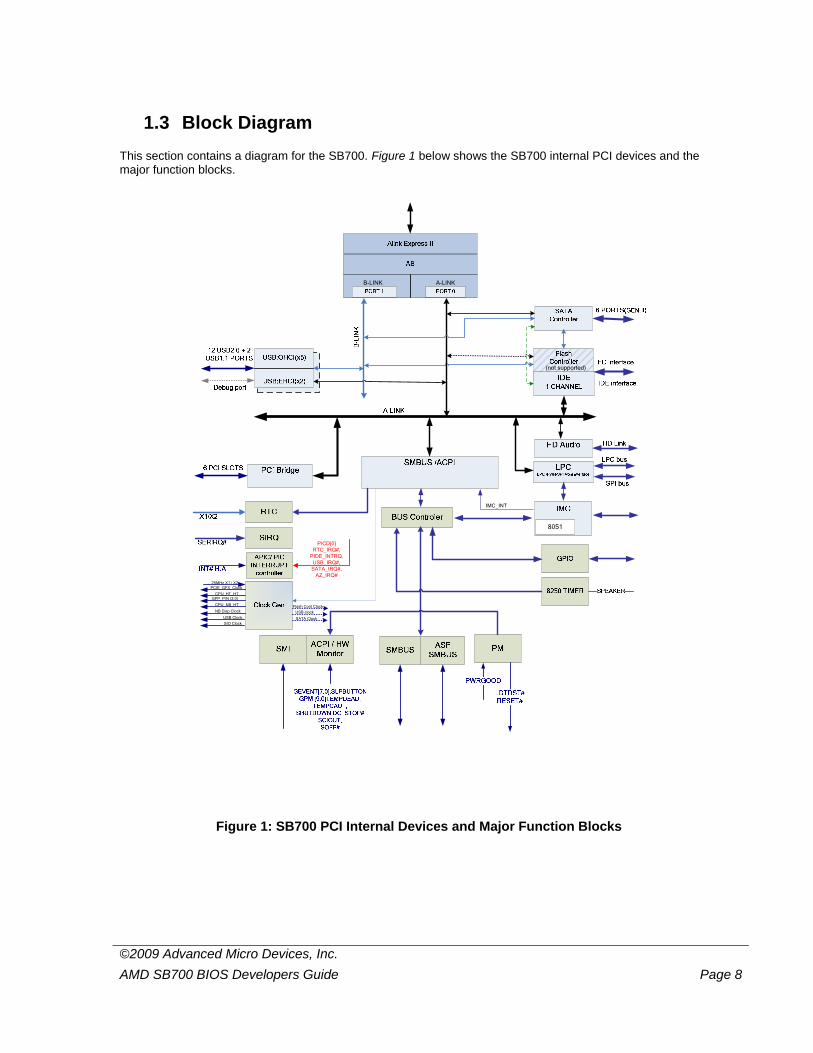
1.3 Block Diagram This section contains a diagram for the SB700. Figure 1 below shows the SB700 internal PCI devices and the major function blocks.
GPP_P/N (3:0)
PICD[0]RTC_IRQ#,
PIDE_INTRQ,USB_IRQ#,
SATA_IRQ#,AZ_IRQ#
B-LINK A-LINK
8051
IMC_INT
CPU_NB_HT
NB Disp Clock
USB Clock
SIO ClockSATA Clock
USB clock
Flash Cont Clock
CPU_HT_HT
PCIE_GFX_Clock25MHz X1 / X2
(not supported)
Figure 1: SB700 PCI Internal Devices and Major Function Blocks
©2009 Advanced Micro Devices, Inc. AMD SB700 BIOS Developers Guide Page 9
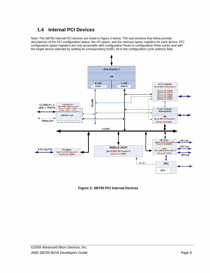
1.4 Internal PCI Devices Note: The SB700 internal PCI devices are listed in Figure 2 below. The sub-sections that follow provide descriptions of the PCI configuration space, the I/O space, and the memory space registers for each device. PCI configuration space registers are only accessible with configuration Read or configuration Write cycles and with the target device selected by settling its corresponding IDSEL bit in the configuration cycle address field.
Figure 2: SB700 PCI Internal Devices
©2009 Advanced Micro Devices, Inc. AMD SB700 BIOS Developers Guide Page 10
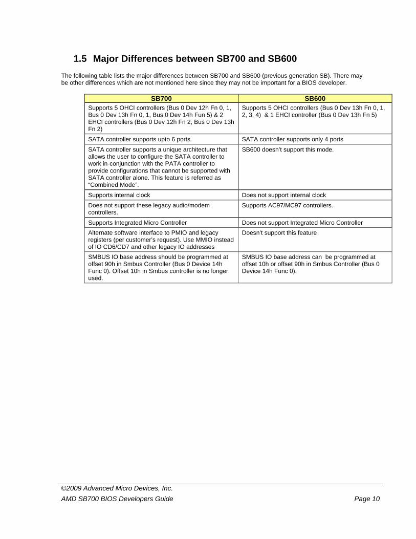
1.5 Major Differences between SB700 and SB600 The following table lists the major differences between SB700 and SB600 (previous generation SB). There may be other differences which are not mentioned here since they may not be important for a BIOS developer.
SB700 SB600 Supports 5 OHCI controllers (Bus 0 Dev 12h Fn 0, 1, Bus 0 Dev 13h Fn 0, 1, Bus 0 Dev 14h Fun 5) & 2 EHCI controllers (Bus 0 Dev 12h Fn 2, Bus 0 Dev 13h Fn 2)
Supports 5 OHCI controllers (Bus 0 Dev 13h Fn 0, 1, 2, 3, 4) & 1 EHCI controller (Bus 0 Dev 13h Fn 5)
SATA controller supports upto 6 ports. SATA controller supports only 4 ports
SATA controller supports a unique architecture that allows the user to configure the SATA controller to work in-conjunction with the PATA controller to provide configurations that cannot be supported with SATA controller alone. This feature is referred as “Combined Mode”.
SB600 doesn’t support this mode.
Supports internal clock Does not support internal clock
Does not support these legacy audio/modem controllers.
Supports AC97/MC97 controllers.
Supports Integrated Micro Controller Does not support Integrated Micro Controller Alternate software interface to PMIO and legacy registers (per customer’s request). Use MMIO instead of IO CD6/CD7 and other legacy IO addresses
Doesn’t support this feature
SMBUS IO base address should be programmed at offset 90h in Smbus Controller (Bus 0 Device 14h Func 0). Offset 10h in Smbus controller is no longer used.
SMBUS IO base address can be programmed at offset 10h or offset 90h in Smbus Controller (Bus 0 Device 14h Func 0).
©2009 Advanced Micro Devices, Inc. AMD SB700 BIOS Developers Guide Page 11
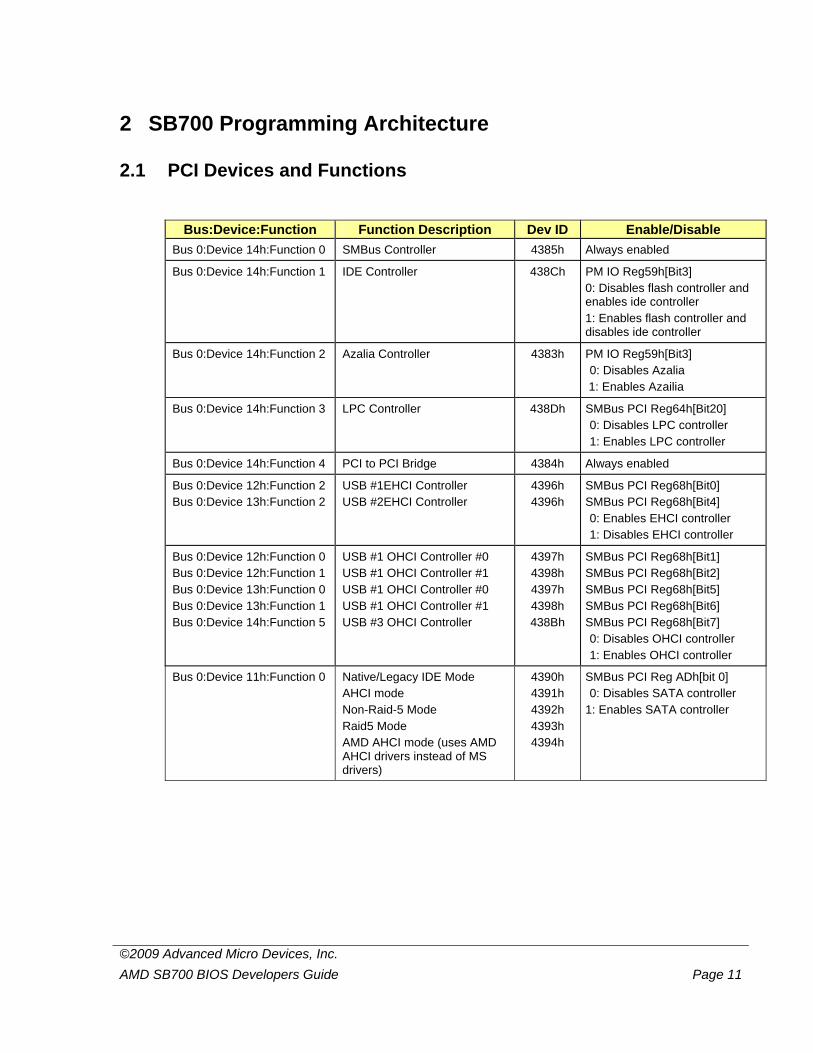
2 SB700 Programming Architecture
2.1 PCI Devices and Functions
Bus:Device:Function Function Description Dev ID Enable/Disable Bus 0:Device 14h:Function 0 SMBus Controller 4385h Always enabled
Bus 0:Device 14h:Function 1 IDE Controller 438Ch PM IO Reg59h[Bit3] 0: Disables flash controller and enables ide controller 1: Enables flash controller and disables ide controller
Bus 0:Device 14h:Function 2 Azalia Controller 4383h PM IO Reg59h[Bit3] 0: Disables Azalia
1: Enables Azailia
Bus 0:Device 14h:Function 3 LPC Controller 438Dh SMBus PCI Reg64h[Bit20] 0: Disables LPC controller 1: Enables LPC controller
Bus 0:Device 14h:Function 4 PCI to PCI Bridge 4384h Always enabled
Bus 0:Device 12h:Function 2 Bus 0:Device 13h:Function 2
USB #1EHCI Controller USB #2EHCI Controller
4396h 4396h
SMBus PCI Reg68h[Bit0] SMBus PCI Reg68h[Bit4] 0: Enables EHCI controller 1: Disables EHCI controller
Bus 0:Device 12h:Function 0 Bus 0:Device 12h:Function 1 Bus 0:Device 13h:Function 0 Bus 0:Device 13h:Function 1 Bus 0:Device 14h:Function 5
USB #1 OHCI Controller #0 USB #1 OHCI Controller #1 USB #1 OHCI Controller #0 USB #1 OHCI Controller #1 USB #3 OHCI Controller
4397h 4398h 4397h 4398h 438Bh
SMBus PCI Reg68h[Bit1] SMBus PCI Reg68h[Bit2] SMBus PCI Reg68h[Bit5] SMBus PCI Reg68h[Bit6] SMBus PCI Reg68h[Bit7] 0: Disables OHCI controller 1: Enables OHCI controller
Bus 0:Device 11h:Function 0 Native/Legacy IDE Mode AHCI mode Non-Raid-5 Mode Raid5 Mode AMD AHCI mode (uses AMD AHCI drivers instead of MS drivers)
4390h 4391h 4392h 4393h 4394h
SMBus PCI Reg ADh[bit 0] 0: Disables SATA controller
1: Enables SATA controller
©2009 Advanced Micro Devices, Inc. AMD SB700 BIOS Developers Guide Page 12
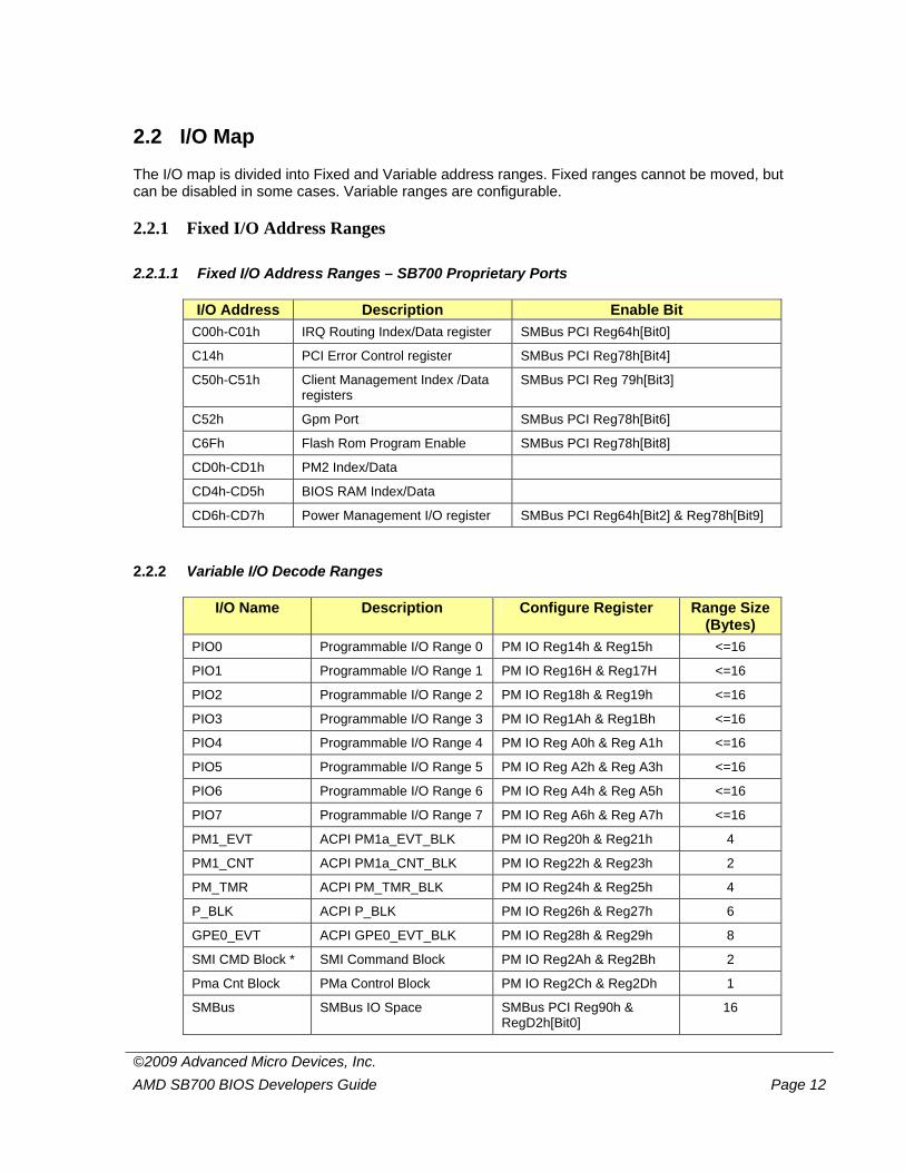
2.2 I/O Map
The I/O map is divided into Fixed and Variable address ranges. Fixed ranges cannot be moved, but can be disabled in some cases. Variable ranges are configurable.
2.2.1 Fixed I/O Address Ranges
2.2.1.1 Fixed I/O Address Ranges – SB700 Proprietary Ports
I/O Address Description Enable Bit C00h-C01h IRQ Routing Index/Data register SMBus PCI Reg64h[Bit0]
C14h PCI Error Control register SMBus PCI Reg78h[Bit4]
C50h-C51h Client Management Index /Data registers
SMBus PCI Reg 79h[Bit3]
C52h Gpm Port SMBus PCI Reg78h[Bit6]
C6Fh Flash Rom Program Enable SMBus PCI Reg78h[Bit8]
CD0h-CD1h PM2 Index/Data
CD4h-CD5h BIOS RAM Index/Data
CD6h-CD7h Power Management I/O register SMBus PCI Reg64h[Bit2] & Reg78h[Bit9]
2.2.2 Variable I/O Decode Ranges
I/O Name Description Configure Register Range Size (Bytes)
PIO0 Programmable I/O Range 0 PM IO Reg14h & Reg15h <=16
PIO1 Programmable I/O Range 1 PM IO Reg16H & Reg17H <=16
PIO2 Programmable I/O Range 2 PM IO Reg18h & Reg19h <=16
PIO3 Programmable I/O Range 3 PM IO Reg1Ah & Reg1Bh <=16
PIO4 Programmable I/O Range 4 PM IO Reg A0h & Reg A1h <=16
PIO5 Programmable I/O Range 5 PM IO Reg A2h & Reg A3h <=16
PIO6 Programmable I/O Range 6 PM IO Reg A4h & Reg A5h <=16
PIO7 Programmable I/O Range 7 PM IO Reg A6h & Reg A7h <=16
PM1_EVT ACPI PM1a_EVT_BLK PM IO Reg20h & Reg21h 4
PM1_CNT ACPI PM1a_CNT_BLK PM IO Reg22h & Reg23h 2
PM_TMR ACPI PM_TMR_BLK PM IO Reg24h & Reg25h 4
P_BLK ACPI P_BLK PM IO Reg26h & Reg27h 6
GPE0_EVT ACPI GPE0_EVT_BLK PM IO Reg28h & Reg29h 8
SMI CMD Block * SMI Command Block PM IO Reg2Ah & Reg2Bh 2
Pma Cnt Block PMa Control Block PM IO Reg2Ch & Reg2Dh 1
SMBus SMBus IO Space SMBus PCI Reg90h & RegD2h[Bit0]
16
©2009 Advanced Micro Devices, Inc. AMD SB700 BIOS Developers Guide Page 13
Note:
• The SMI CMD Block must be defined on the 16-bit boundary, i.e., the least significant nibble of the address must be zero (for example, B0h, C0h etc.)
• The SMI CMD Block consists of two ports – the SMI Command Port at base address, and the SMI Status Port at base address+1.
• The writes to SMI Status Port will not generate an SMI. The writes to the SMI Command Port will generate an SMI.
• The SMI Command and SMI Status ports may be written individually as 8 bit ports, or together as a 16-bit port.
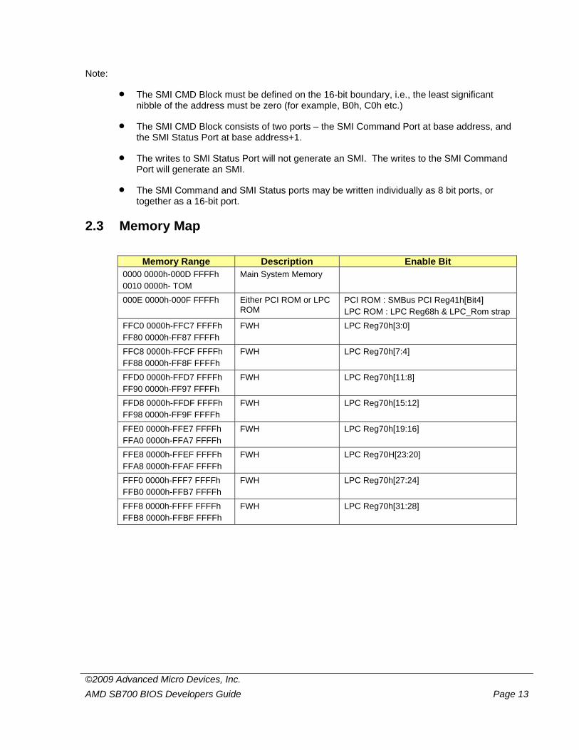
2.3 Memory Map
Memory Range Description Enable Bit
0000 0000h-000D FFFFh 0010 0000h- TOM
Main System Memory
000E 0000h-000F FFFFh Either PCI ROM or LPC ROM
PCI ROM : SMBus PCI Reg41h[Bit4] LPC ROM : LPC Reg68h & LPC_Rom strap
FFC0 0000h-FFC7 FFFFh FF80 0000h-FF87 FFFFh
FWH LPC Reg70h[3:0]
FFC8 0000h-FFCF FFFFh FF88 0000h-FF8F FFFFh
FWH LPC Reg70h[7:4]
FFD0 0000h-FFD7 FFFFh FF90 0000h-FF97 FFFFh
FWH LPC Reg70h[11:8]
FFD8 0000h-FFDF FFFFh FF98 0000h-FF9F FFFFh
FWH LPC Reg70h[15:12]
FFE0 0000h-FFE7 FFFFh FFA0 0000h-FFA7 FFFFh
FWH LPC Reg70h[19:16]
FFE8 0000h-FFEF FFFFh FFA8 0000h-FFAF FFFFh
FWH LPC Reg70H[23:20]
FFF0 0000h-FFF7 FFFFh FFB0 0000h-FFB7 FFFFh
FWH LPC Reg70h[27:24]
FFF8 0000h-FFFF FFFFh FFB8 0000h-FFBF FFFFh
FWH LPC Reg70h[31:28]
©2009 Advanced Micro Devices, Inc. AMD SB700 BIOS Developers Guide Page 14
3 SB700 Early-POST Initialization
The system BIOS needs to configure the SB700 at the very beginning of POST. Some of the settings will change depending on the OEM design, or on the newer revision chipset.
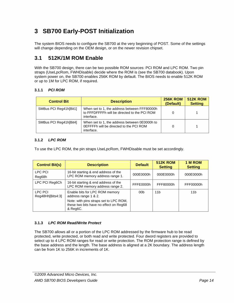
3.1 512K/1M ROM Enable
With the SB700 design, there can be two possible ROM sources: PCI ROM and LPC ROM. Two pin straps (UseLpcRom, FWHDisable) decide where the ROM is (see the SB700 databook). Upon system power on, the SB700 enables 256K ROM by default. The BIOS needs to enable 512K ROM or up to 1M for LPC ROM, if required.
3.1.1 PCI ROM
Control Bit Description 256K ROM (Default)
512K ROM Setting
SMBus PCI Reg41h[Bit1] When set to 1, the address between FFF80000h to FFFDFFFFh will be directed to the PCI ROM interface.
0 1
SMBus PCI Reg41h[Bit4] When set to 1, the address between 0E0000h to 0EFFFFh will be directed to the PCI ROM interface.
0 1
3.1.2 LPC ROM
To use the LPC ROM, the pin straps UseLpcRom, FWHDisable must be set accordingly.
Control Bit(s) Description Default 512K ROM Setting
1 M ROM Setting
LPC PCI Reg68h
16-bit starting & end address of the LPC ROM memory address range 1. 000E0000h 000E0000h 000E0000h
LPC PCI Reg6Ch 16-bit starting & end address of the LPC ROM memory address range 2. FFFE0000h FFF80000h FFF00000h
LPC PCI Reg48Hh[Bits4:3]
Enable bits for LPC ROM memory address range 1 & 2. Note: with pins straps set to LPC ROM, these two bits have no effect on Reg68 & Reg6C.
00b 11b 11b
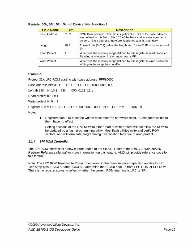
3.1.3 LPC ROM Read/Write Protect
The SB700 allows all or a portion of the LPC ROM addressed by the firmware hub to be read protected, write protected, or both read and write protected. Four dword registers are provided to select up to 4 LPC ROM ranges for read or write protection. The ROM protection range is defined by the base address and the length. The base address is aligned at a 2K boundary. The address length can be from 1K to 256K in increments of 1K.
©2009 Advanced Micro Devices, Inc. AMD SB700 BIOS Developers Guide Page 15
Register 50h, 54h, 58h, 5ch of Device 14h, Function 3
Field Name Bits Description Base Address 31:11 ROM Base address. The most significant 21 bits of the base address
are defined in this field. Bits 10:0 of the base address are assumed to be zero. Base address, therefore, is aligned at a 2K boundary.
Length 10:2 These 9 bits (0-511) define the length from 1K to 512K in increments of 1K.
Read Protect 1 When set, the memory range defined by this register is read protected. Reading any location in the range returns FFh.
Write Protect 0 When set, the memory range defined by this register is write protected. Writing to the range has no effect.
Example:
Protect 32K LPC ROM starting with base address FFF80000.
Base address bits 31:11 1111 1111 1111 1000 0000 0 b
Length 32K bit 10:2 = 31h = 000 0111 11 b
Read protect bit 1 = 1
Write protect bit 0 = 1
Register 50h = 1111 1111 1111 1000 0000 0000 0111 1111 b = FFF8007F h
Note:
1. Registers 50h ~ 5Fh can be written once after the hardware reset. Subsequent writes to them have no effect.
2. Setting sections of the LPC ROM to either read or write protect will not allow the ROM to be updated by a flash programming utility. Most flash utilities write and verify ROM sectors, and will terminate programming if verification fails due to read protect.
3.1.4 SPI ROM Controller
The SPI ROM interface is a new feature added to the SB700. Refer to the AMD SB700/710/750 Register Reference Manual for more information on this feature. AMD will provide reference code for this feature. Note: The LPC ROM Read/Write Protect mentioned in the previous paragraph also applies to SPI. Two strap pins, PCICLK0 and PCICLK1, determine the SB700 boot up from LPC ROM or SPI ROM. There is no register status to reflect whether the current ROM interface is LPC or SPI.
©2009 Advanced Micro Devices, Inc. AMD SB700 BIOS Developers Guide Page 16
3.2 Real Time Clock (RTC)
3.2.1 RTC Access
The internal RTC is divided into two sections: the clock and alarm function (registers 0 to 0Dh), and CMOS memory (registers 0Eh to FFh). The clock and alarm functions must be accessed through I/O ports 70h/71h. The CMOS memory (registers 0Eh to FFh) should be accessed through I/O ports 72h/73h.
3.2.1.1 Special Locked Area in CMOS
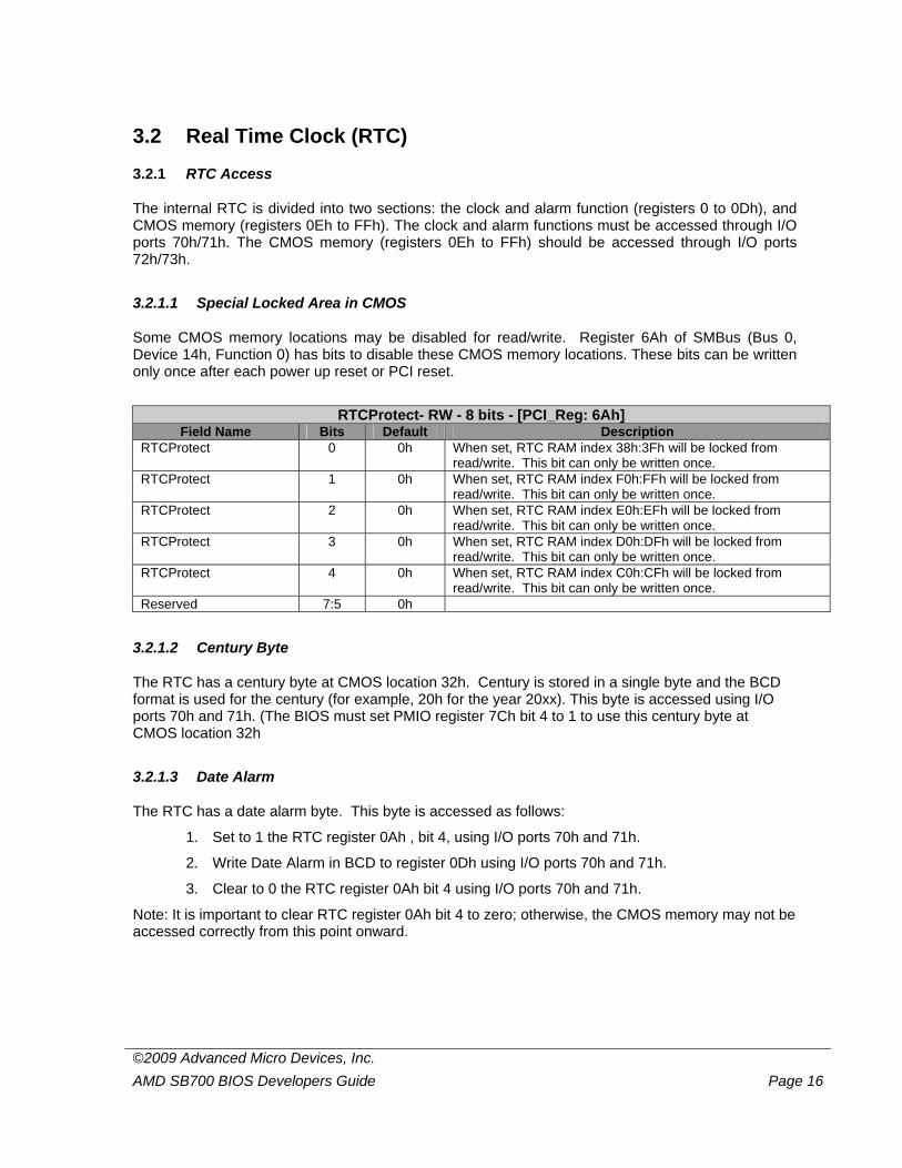
Some CMOS memory locations may be disabled for read/write. Register 6Ah of SMBus (Bus 0, Device 14h, Function 0) has bits to disable these CMOS memory locations. These bits can be written only once after each power up reset or PCI reset.
RTCProtect- RW - 8 bits - [PCI_Reg: 6Ah]
Field Name Bits Default Description RTCProtect 0 0h When set, RTC RAM index 38h:3Fh will be locked from
read/write. This bit can only be written once. RTCProtect 1 0h When set, RTC RAM index F0h:FFh will be locked from
read/write. This bit can only be written once. RTCProtect 2 0h When set, RTC RAM index E0h:EFh will be locked from
read/write. This bit can only be written once. RTCProtect 3 0h When set, RTC RAM index D0h:DFh will be locked from
read/write. This bit can only be written once. RTCProtect 4 0h When set, RTC RAM index C0h:CFh will be locked from
read/write. This bit can only be written once. Reserved 7:5 0h
3.2.1.2 Century Byte
The RTC has a century byte at CMOS location 32h. Century is stored in a single byte and the BCD format is used for the century (for example, 20h for the year 20xx). This byte is accessed using I/O ports 70h and 71h. (The BIOS must set PMIO register 7Ch bit 4 to 1 to use this century byte at CMOS location 32h
3.2.1.3 Date Alarm
The RTC has a date alarm byte. This byte is accessed as follows:
1. Set to 1 the RTC register 0Ah , bit 4, using I/O ports 70h and 71h.
2. Write Date Alarm in BCD to register 0Dh using I/O ports 70h and 71h.
3. Clear to 0 the RTC register 0Ah bit 4 using I/O ports 70h and 71h.
Note: It is important to clear RTC register 0Ah bit 4 to zero; otherwise, the CMOS memory may not be accessed correctly from this point onward.
©2009 Advanced Micro Devices, Inc. AMD SB700 BIOS Developers Guide Page 17
3.3 BIOS RAM
The SB700 has 256 bytes of BIOS RAM. Data in this RAM is preserved until RSMRST# or S5 is asserted, or until power is lost.
This RAM is accessed using index and data registers at CD4h/CD5h.
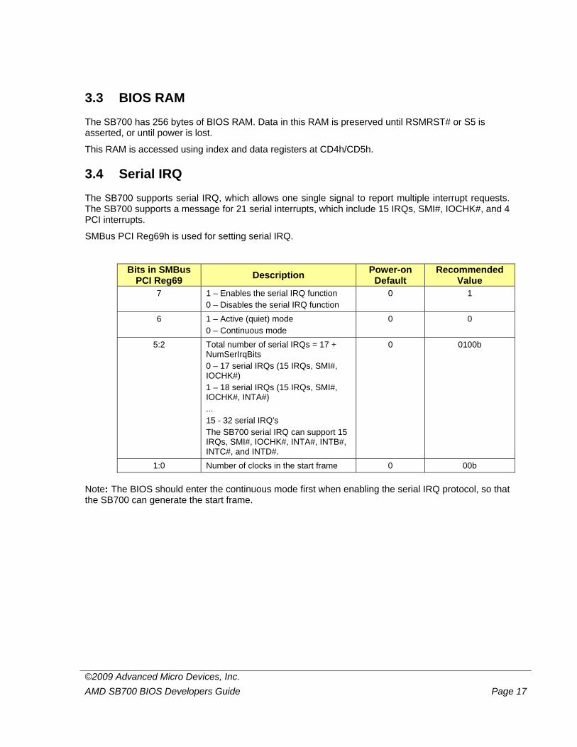
3.4 Serial IRQ
The SB700 supports serial IRQ, which allows one single signal to report multiple interrupt requests. The SB700 supports a message for 21 serial interrupts, which include 15 IRQs, SMI#, IOCHK#, and 4 PCI interrupts.
SMBus PCI Reg69h is used for setting serial IRQ.
Bits in SMBus PCI Reg69 Description Power-on
Default Recommended
Value 7 1 – Enables the serial IRQ function
0 – Disables the serial IRQ function 0 1
6 1 – Active (quiet) mode 0 – Continuous mode
0 0
5:2 Total number of serial IRQs = 17 + NumSerIrqBits 0 – 17 serial IRQs (15 IRQs, SMI#, IOCHK#) 1 – 18 serial IRQs (15 IRQs, SMI#, IOCHK#, INTA#) ... 15 - 32 serial IRQ's The SB700 serial IRQ can support 15 IRQs, SMI#, IOCHK#, INTA#, INTB#, INTC#, and INTD#.
0 0100b
1:0 Number of clocks in the start frame 0 00b Note: The BIOS should enter the continuous mode first when enabling the serial IRQ protocol, so that the SB700 can generate the start frame.
©2009 Advanced Micro Devices, Inc. AMD SB700 BIOS Developers Guide Page 18
3.5 SubSystem ID and SubSystem Vendor ID
SubSytem ID and SubSystem Vendor ID can be programmed in various functions of SB700 register 2Ch. These registers are write-once registers. For example, to program a SubSytem vendor ID of 1002h and SubSystem ID of 4341h in AC97 device 14h, function 5, use the following assembly language sample code:
mov eax,8000A52Ch
mov dx,0CF8h
out dx,eax
mov dx,0CFCh
mov eax,43411002h
out dx,eax
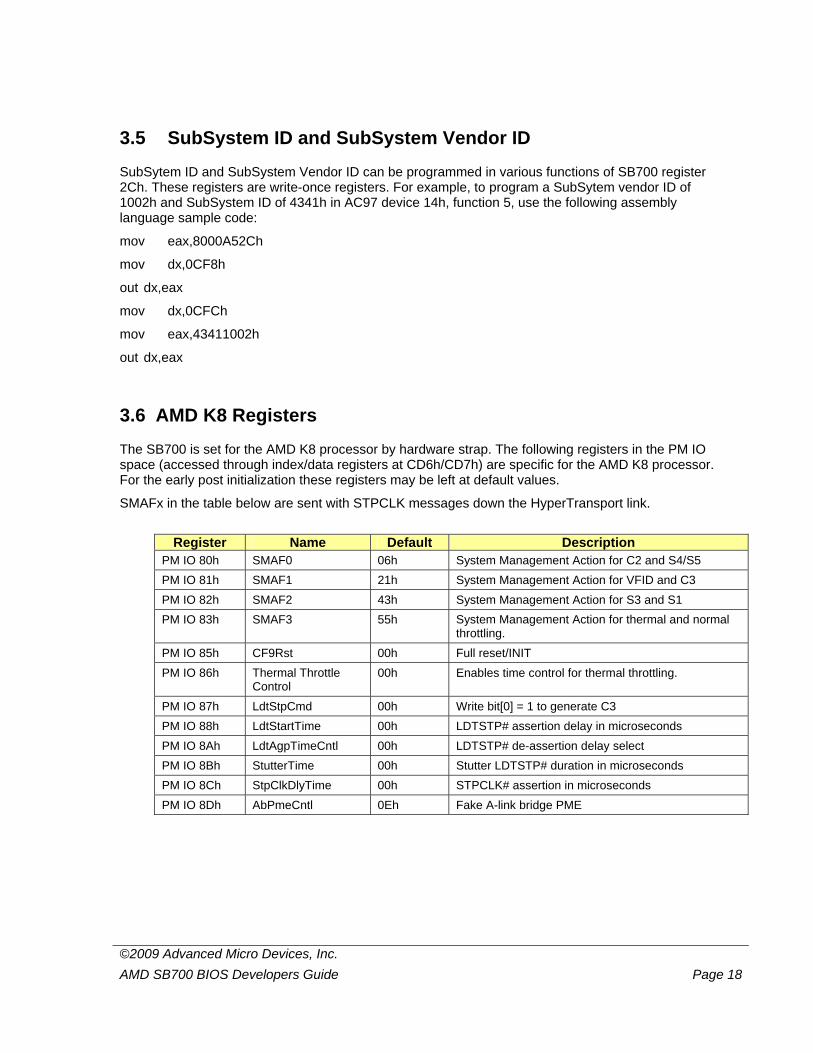
3.6 AMD K8 Registers
The SB700 is set for the AMD K8 processor by hardware strap. The following registers in the PM IO space (accessed through index/data registers at CD6h/CD7h) are specific for the AMD K8 processor. For the early post initialization these registers may be left at default values.
SMAFx in the table below are sent with STPCLK messages down the HyperTransport link.
Register Name Default Description
PM IO 80h SMAF0 06h System Management Action for C2 and S4/S5 PM IO 81h SMAF1 21h System Management Action for VFID and C3 PM IO 82h SMAF2 43h System Management Action for S3 and S1 PM IO 83h SMAF3 55h System Management Action for thermal and normal
throttling. PM IO 85h CF9Rst 00h Full reset/INIT PM IO 86h Thermal Throttle
Control 00h Enables time control for thermal throttling.
PM IO 87h LdtStpCmd 00h Write bit[0] = 1 to generate C3 PM IO 88h LdtStartTime 00h LDTSTP# assertion delay in microseconds PM IO 8Ah LdtAgpTimeCntl 00h LDTSTP# de-assertion delay select PM IO 8Bh StutterTime 00h Stutter LDTSTP# duration in microseconds PM IO 8Ch StpClkDlyTime 00h STPCLK# assertion in microseconds PM IO 8Dh AbPmeCntl 0Eh Fake A-link bridge PME
©2009 Advanced Micro Devices, Inc. AMD SB700 BIOS Developers Guide Page 19
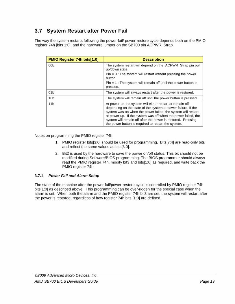
3.7 System Restart after Power Fail
The way the system restarts following the power-fail/ power-restore cycle depends both on the PMIO register 74h [bits 1:0], and the hardware jumper on the SB700 pin ACPWR_Strap.
PMIO Register 74h bits[1:0] Description 00b The system restart will depend on the ACPWR_Strap pin pull
up/down state. Pin = 0 : The system will restart without pressing the power button Pin = 1 : The system will remain off until the power button in pressed.
01b The system will always restart after the power is restored. 10b The system will remain off until the power button is pressed. 11b At power-up the system will either restart or remain off
depending on the state of the system at power failure. If the system was on when the power failed, the system will restart at power-up. If the system was off when the power failed, the system will remain off after the power is restored. Pressing the power button is required to restart the system.
Notes on programming the PMIO register 74h:
1. PMIO register bits[3:0] should be used for programming. Bits[7:4] are read-only bits and reflect the same values as bits[3:0].
2. Bit2 is used by the hardware to save the power on/off status. This bit should not be modified during Software/BIOS programming. The BIOS programmer should always read the PMIO register 74h, modify bit3 and bits[1:0] as required, and write back the PMIO register 74h.
3.7.1 Power Fail and Alarm Setup
The state of the machine after the power-fail/power-restore cycle is controlled by PMIO register 74h bits[1:0] as described above. This programming can be over-ridden for the special case when the alarm is set. When both the alarm and the PMIO register 74h bit3 are set, the system will restart after the power is restored, regardless of how register 74h bits [1:0] are defined.
©2009 Advanced Micro Devices, Inc. AMD SB700 BIOS Developers Guide Page 20
4 PCI IRQ Routing
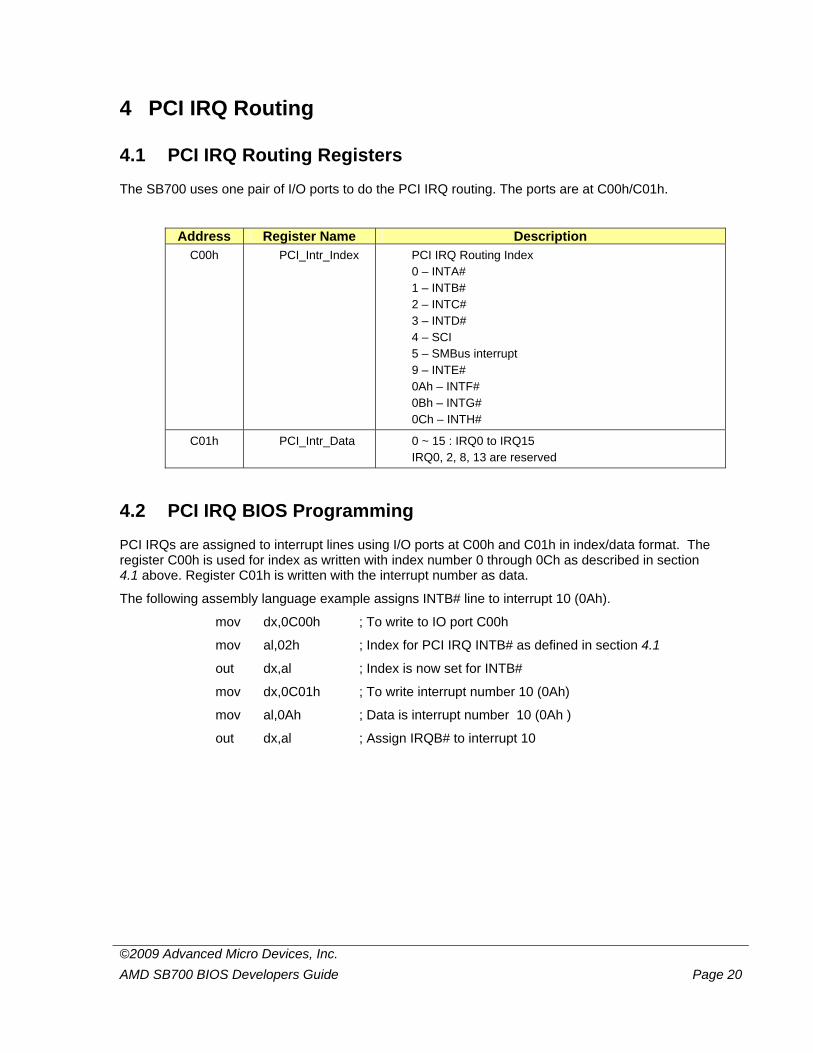
4.1 PCI IRQ Routing Registers
The SB700 uses one pair of I/O ports to do the PCI IRQ routing. The ports are at C00h/C01h.
Address Register Name Description C00h PCI_Intr_Index PCI IRQ Routing Index
0 – INTA# 1 – INTB# 2 – INTC# 3 – INTD# 4 – SCI 5 – SMBus interrupt 9 – INTE# 0Ah – INTF# 0Bh – INTG# 0Ch – INTH#
C01h PCI_Intr_Data 0 ~ 15 : IRQ0 to IRQ15 IRQ0, 2, 8, 13 are reserved
4.2 PCI IRQ BIOS Programming
PCI IRQs are assigned to interrupt lines using I/O ports at C00h and C01h in index/data format. The register C00h is used for index as written with index number 0 through 0Ch as described in section 4.1 above. Register C01h is written with the interrupt number as data.
The following assembly language example assigns INTB# line to interrupt 10 (0Ah).
mov dx,0C00h ; To write to IO port C00h
mov al,02h ; Index for PCI IRQ INTB# as defined in section 4.1
out dx,al ; Index is now set for INTB#
mov dx,0C01h ; To write interrupt number 10 (0Ah)
mov al,0Ah ; Data is interrupt number 10 (0Ah )
out dx,al ; Assign IRQB# to interrupt 10
©2009 Advanced Micro Devices, Inc. AMD SB700 BIOS Developers Guide Page 21
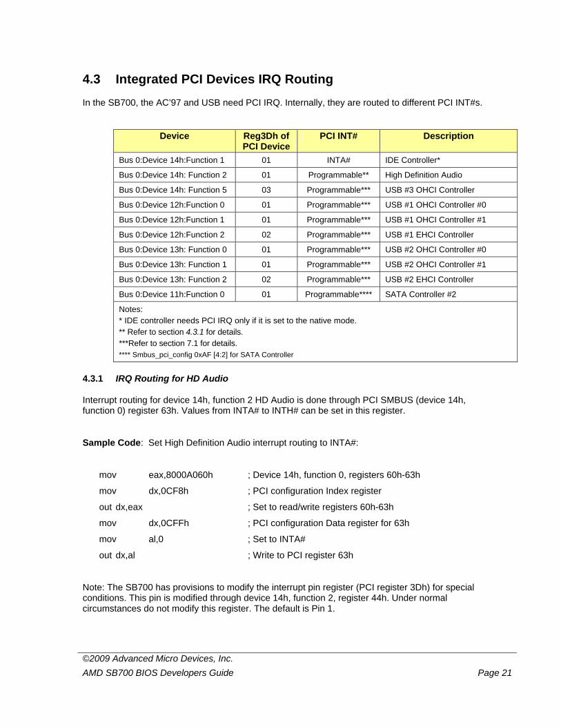
4.3 Integrated PCI Devices IRQ Routing
In the SB700, the AC’97 and USB need PCI IRQ. Internally, they are routed to different PCI INT#s.
Device Reg3Dh of PCI Device
PCI INT# Description
Bus 0:Device 14h:Function 1 01 INTA# IDE Controller*
Bus 0:Device 14h: Function 2 01 Programmable** High Definition Audio
Bus 0:Device 14h: Function 5 03 Programmable*** USB #3 OHCI Controller
Bus 0:Device 12h:Function 0 01 Programmable*** USB #1 OHCI Controller #0
Bus 0:Device 12h:Function 1 01 Programmable*** USB #1 OHCI Controller #1
Bus 0:Device 12h:Function 2 02 Programmable*** USB #1 EHCI Controller
Bus 0:Device 13h: Function 0 01 Programmable*** USB #2 OHCI Controller #0
Bus 0:Device 13h: Function 1 01 Programmable*** USB #2 OHCI Controller #1
Bus 0:Device 13h: Function 2 02 Programmable*** USB #2 EHCI Controller
Bus 0:Device 11h:Function 0 01 Programmable**** SATA Controller #2
Notes: * IDE controller needs PCI IRQ only if it is set to the native mode. ** Refer to section 4.3.1 for details. ***Refer to section 7.1 for details. **** Smbus_pci_config 0xAF [4:2] for SATA Controller
4.3.1 IRQ Routing for HD Audio
Interrupt routing for device 14h, function 2 HD Audio is done through PCI SMBUS (device 14h, function 0) register 63h. Values from INTA# to INTH# can be set in this register.
Sample Code: Set High Definition Audio interrupt routing to INTA#:
mov eax,8000A060h ; Device 14h, function 0, registers 60h-63h
mov dx,0CF8h ; PCI configuration Index register
out dx,eax ; Set to read/write registers 60h-63h
mov dx,0CFFh ; PCI configuration Data register for 63h
mov al,0 ; Set to INTA#
out dx,al ; Write to PCI register 63h
Note: The SB700 has provisions to modify the interrupt pin register (PCI register 3Dh) for special conditions. This pin is modified through device 14h, function 2, register 44h. Under normal circumstances do not modify this register. The default is Pin 1.
©2009 Advanced Micro Devices, Inc. AMD SB700 BIOS Developers Guide Page 22
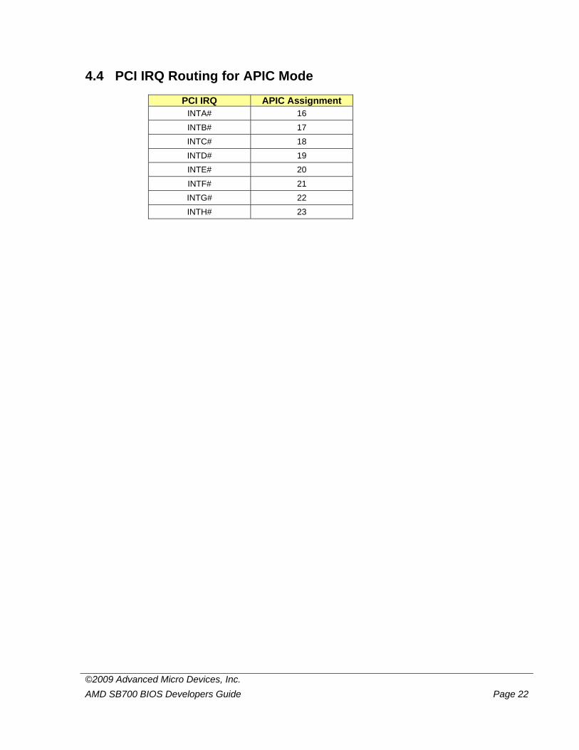
4.4 PCI IRQ Routing for APIC Mode
PCI IRQ APIC Assignment INTA# 16 INTB# 17 INTC# 18 INTD# 19 INTE# 20 INTF# 21 INTG# 22 INTH# 23
©2009 Advanced Micro Devices, Inc. AMD SB700 BIOS Developers Guide Page 23
5 SMBus Programming
The SB700 SMBus (System Management Bus) complies with SMBus Specification Version 2.0.
5.1 SMBus I/O Base Address
The BIOS needs to set a valid SMBus I/O base address before enabling the SMBus Controller. The SMBus I/0 base address should be set at PCI Reg90h in the SMBus Controller (Bus 0, Device 14h, Function 0).
The SMBus controller enable bit is bit 0, register D2h, of the SMBus device (Bus 0, Device 14h, Function 0).
The following is a sample code to enable the SMBus with a temporary I/O base address:
SMB_IO EQU 8040h
; Set SMBus I/O base address
mov dx, 0CF8h ; PCI Index Register
mov eax, 8000A090h ; Reg90h on SMBus PCI Controller
out dx, eax
mov dx, 0CFCh ; PCI Data Register
mov eax, SMB_IO ; Temp SMBus I/O base address
out dx, eax
; Enable the SMBus controller
mov dx, 0CF8h ; PCI Index Register
mov eax, 8000A0D0h ; RegD0 on SMBus PCI Controller
out dx, eax
mov dx, 0CFEh ; PCI Data Register
in al, dx ; Read back from RegD2h
or al, 01 ; Bit [0] for enabling SMBus Controller interface
out dx, al
5.2 SMBus Timing
The SMBus frequency can be adjusted using different values in an 8-bit I/O register at the SMBus base + 0Eh location.
The SMBus frequency is set as follows:
SMBus Frequency = (Primary Alink Clock )/(Count in index 0Eh * 4)
The power-up default value in register 0Eh is A0h, therefore the default frequency is (66MHz)/(160 * 4), or approximately 103 KHz.
The minimum SMBus frequency can be set with the value FFh in the register at index 0Eh, which yields the following: (66MHz)/(255*4) = 64.7 KHz.
©2009 Advanced Micro Devices, Inc. AMD SB700 BIOS Developers Guide Page 24
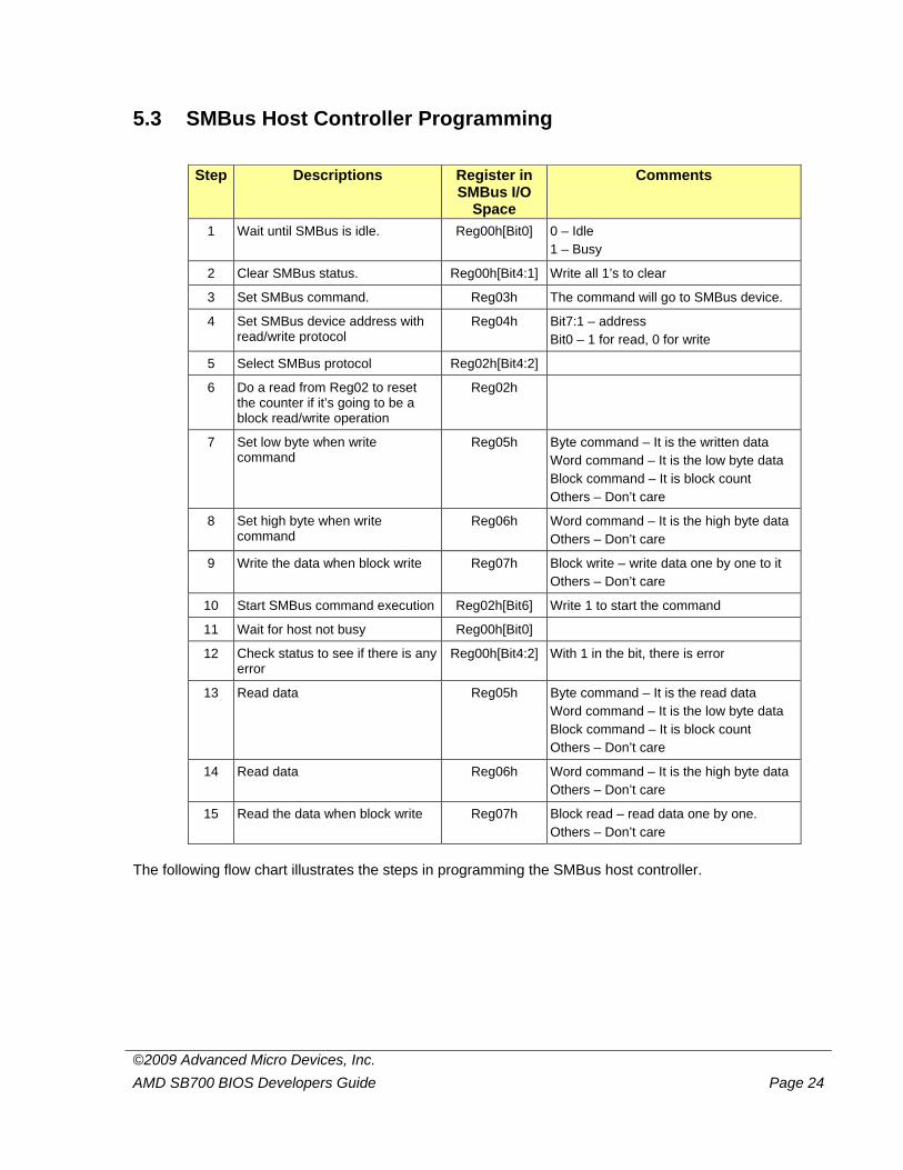
5.3 SMBus Host Controller Programming
Step Descriptions Register in
SMBus I/O Space
Comments
1 Wait until SMBus is idle. Reg00h[Bit0] 0 – Idle 1 – Busy
2 Clear SMBus status. Reg00h[Bit4:1] Write all 1’s to clear
3 Set SMBus command. Reg03h The command will go to SMBus device.
4 Set SMBus device address with read/write protocol
Reg04h Bit7:1 – address Bit0 – 1 for read, 0 for write
5 Select SMBus protocol Reg02h[Bit4:2]
6 Do a read from Reg02 to reset the counter if it’s going to be a block read/write operation
Reg02h
7 Set low byte when write command
Reg05h Byte command – It is the written data Word command – It is the low byte data Block command – It is block count Others – Don’t care
8 Set high byte when write command
Reg06h Word command – It is the high byte data Others – Don’t care
9 Write the data when block write Reg07h Block write – write data one by one to it Others – Don’t care
10 Start SMBus command execution Reg02h[Bit6] Write 1 to start the command
11 Wait for host not busy Reg00h[Bit0]
12 Check status to see if there is any error
Reg00h[Bit4:2] With 1 in the bit, there is error
13 Read data Reg05h Byte command – It is the read data Word command – It is the low byte data Block command – It is block count Others – Don’t care
14 Read data Reg06h Word command – It is the high byte data Others – Don’t care
15 Read the data when block write Reg07h Block read – read data one by one. Others – Don’t care
The following flow chart illustrates the steps in programming the SMBus host controller.
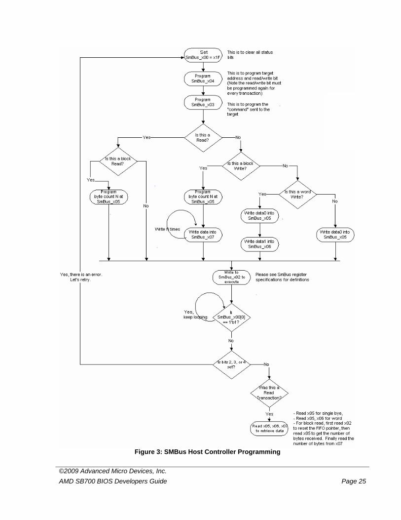
©2009 Advanced Micro Devices, Inc. AMD SB700 BIOS Developers Guide Page 25
Figure 3: SMBus Host Controller Programming
©2009 Advanced Micro Devices, Inc. AMD SB700 BIOS Developers Guide Page 26
6 IDE Controller
The SB700 IDE controller supports Ultra ATA 33/66/100/133 modes. The IDE controller can be configured into either the compatible mode or the native mode. Under the compatible mode, the IDE controller will use the legacy resources.
The SB700 allows programming of the IDE timing and mode for each drive independently on each channel.
6.1 IDE Channel Enable/Disable
Register on IDE Controller
Bit Description
Reg09h 1 Primary IDE channel programmable logic enable. Reg48h 0 Set 1 to disable the primary IDE channel. Reg48h 8 Set 1 to disable the secondary IDE channel.
With the SB700, the BIOS must follow particular sequences to enable or disable the IDE channels (see section 6.1.1 and 6.1.2 below for further information).
6.1.1 IDE Channel Enable
Both of the IDE channels are enabled as power-on default. To enable an IDE channel, the BIOS must be set as follows:
1. Set the IDE channel programmable logic enable bit in Reg09h. 2. Clear the IDE channel disable bit in Reg48h to enable the IDE channel.
Note: No IDE I/O port access is allowed in between step (1) and step (2). It is recommended that the BIOS execute step (2) immediately after step (1).
Refer to section 14.3.5 for a programming sample.
6.1.2 IDE Channel Disable
To disable an IDE channel, the BIOS must:
1. Set IDE channel programmable logic enable bit in Reg09h. 2. Set IDE channel disable bit in Reg48h to disable IDE channel.
Note: No IDE I/O port access is allowed in between step (1) and (2). It’s recommended that the BIOS execute step (2) immediately after step (1).
Note: Secondary IDE channel should always be disabled for there is no pin out for secondary IDE.
After the IDE disable sequence, the IDE channel programmable logic enable bit will be cleared automatically.
Refer to section 14.3.4 for a programming sample.
©2009 Advanced Micro Devices, Inc. AMD SB700 BIOS Developers Guide Page 27
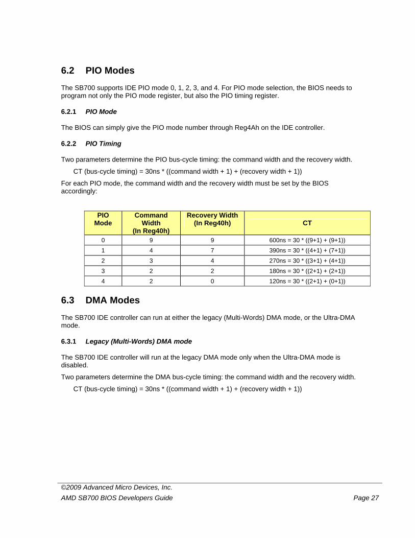
6.2 PIO Modes
The SB700 supports IDE PIO mode 0, 1, 2, 3, and 4. For PIO mode selection, the BIOS needs to program not only the PIO mode register, but also the PIO timing register.
6.2.1 PIO Mode
The BIOS can simply give the PIO mode number through Reg4Ah on the IDE controller.
6.2.2 PIO Timing
Two parameters determine the PIO bus-cycle timing: the command width and the recovery width.
CT (bus-cycle timing) = 30ns * ((command width + 1) + (recovery width + 1))
For each PIO mode, the command width and the recovery width must be set by the BIOS accordingly:
PIO Mode
Command Width
(In Reg40h)
Recovery Width (In Reg40h) CT
0 9 9 600ns = 30 * ((9+1) + (9+1))
1 4 7 390ns = 30 * ((4+1) + (7+1))
2 3 4 270ns = 30 * ((3+1) + (4+1))
3 2 2 180ns = 30 * ((2+1) + (2+1))
4 2 0 120ns = 30 * ((2+1) + (0+1))
6.3 DMA Modes
The SB700 IDE controller can run at either the legacy (Multi-Words) DMA mode, or the Ultra-DMA mode.
6.3.1 Legacy (Multi-Words) DMA mode
The SB700 IDE controller will run at the legacy DMA mode only when the Ultra-DMA mode is disabled.
Two parameters determine the DMA bus-cycle timing: the command width and the recovery width.
CT (bus-cycle timing) = 30ns * ((command width + 1) + (recovery width + 1))
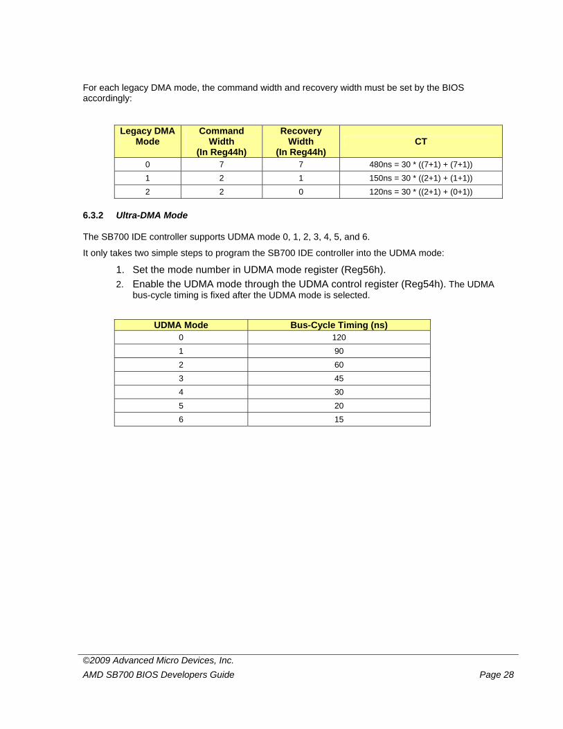
©2009 Advanced Micro Devices, Inc. AMD SB700 BIOS Developers Guide Page 28
For each legacy DMA mode, the command width and recovery width must be set by the BIOS accordingly:
Legacy DMA Mode
Command Width
(In Reg44h)
Recovery Width
(In Reg44h) CT
0 7 7 480ns = 30 * ((7+1) + (7+1)) 1 2 1 150ns = 30 * ((2+1) + (1+1)) 2 2 0 120ns = 30 * ((2+1) + (0+1))
6.3.2 Ultra-DMA Mode
The SB700 IDE controller supports UDMA mode 0, 1, 2, 3, 4, 5, and 6.
It only takes two simple steps to program the SB700 IDE controller into the UDMA mode:
1. Set the mode number in UDMA mode register (Reg56h). 2. Enable the UDMA mode through the UDMA control register (Reg54h). The UDMA
bus-cycle timing is fixed after the UDMA mode is selected.
UDMA Mode Bus-Cycle Timing (ns) 0 120 1 90 2 60 3 45 4 30 5 20 6 15
©2009 Advanced Micro Devices, Inc. AMD SB700 BIOS Developers Guide Page 29
7 USB Controllers
7.1 Interrupt Routing for USB Controllers
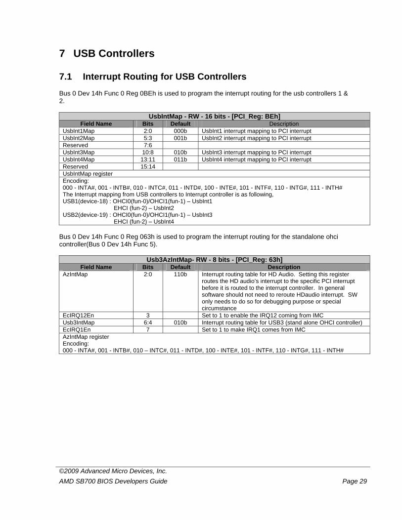
Bus 0 Dev 14h Func 0 Reg 0BEh is used to program the interrupt routing for the usb controllers 1 & 2.
UsbIntMap - RW - 16 bits - [PCI_Reg: BEh] Field Name Bits Default Description
UsbInt1Map 2:0 000b UsbInt1 interrupt mapping to PCI interrupt UsbInt2Map 5:3 001b UsbInt2 interrupt mapping to PCI interrupt Reserved 7:6 UsbInt3Map 10:8 010b UsbInt3 interrupt mapping to PCI interrupt UsbInt4Map 13:11 011b UsbInt4 interrupt mapping to PCI interrupt Reserved 15:14 UsbIntMap register Encoding: 000 - INTA#, 001 - INTB#, 010 - INTC#, 011 - INTD#, 100 - INTE#, 101 - INTF#, 110 - INTG#, 111 - INTH# The Interrupt mapping from USB controllers to Interrupt controller is as following, USB1(device-18) : OHCI0(fun-0)/OHCI1(fun-1) – UsbInt1 EHCI (fun-2) – UsbInt2 USB2(device-19) : OHCI0(fun-0)/OHCI1(fun-1) – UsbInt3 EHCI (fun-2) – UsbInt4
Bus 0 Dev 14h Func 0 Reg 063h is used to program the interrupt routing for the standalone ohci controller(Bus 0 Dev 14h Func 5).
Usb3AzIntMap- RW - 8 bits - [PCI_Reg: 63h] Field Name Bits Default Description
AzIntMap 2:0 110b Interrupt routing table for HD Audio. Setting this register routes the HD audio’s interrupt to the specific PCI interrupt before it is routed to the interrupt controller. In general software should not need to reroute HDaudio interrupt. SW only needs to do so for debugging purpose or special circumstance
EcIRQ12En 3 Set to 1 to enable the IRQ12 coming from IMC Usb3IntMap 6:4 010b Interrupt routing table for USB3 (stand alone OHCI controller) EcIRQ1En 7 Set to 1 to make IRQ1 comes from IMC AzIntMap register Encoding: 000 - INTA#, 001 - INTB#, 010 – INTC#, 011 - INTD#, 100 - INTE#, 101 - INTF#, 110 - INTG#, 111 - INTH#
©2009 Advanced Micro Devices, Inc. AMD SB700 BIOS Developers Guide Page 30
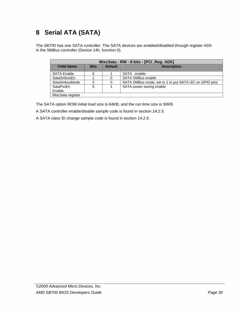
8 Serial ATA (SATA)
The SB700 has one SATA controller. The SATA devices are enabled/disabled through register ADh in the SMBus controller (Device 14h, function 0).
MiscSata - RW - 8 bits - [PCI_Reg: ADh]
Field Name Bits Default Description
SATA Enable 0 1 SATA enable SataSmbusEn 1 0 SATA SMBus enable SataSmbusMode 2 0 SATA SMBus mode, set to 1 to put SATA I2C on GPIO pins SataPsvEn Enable
5 1 SATA power saving enable
MiscSata register The SATA option ROM initial load size is 64KB, and the run time size is 50KB.
A SATA controller enable/disable sample code is found in section 14.2.5.
A SATA class ID change sample code is found in section 14.2.6.
©2009 Advanced Micro Devices, Inc. AMD SB700 BIOS Developers Guide Page 31
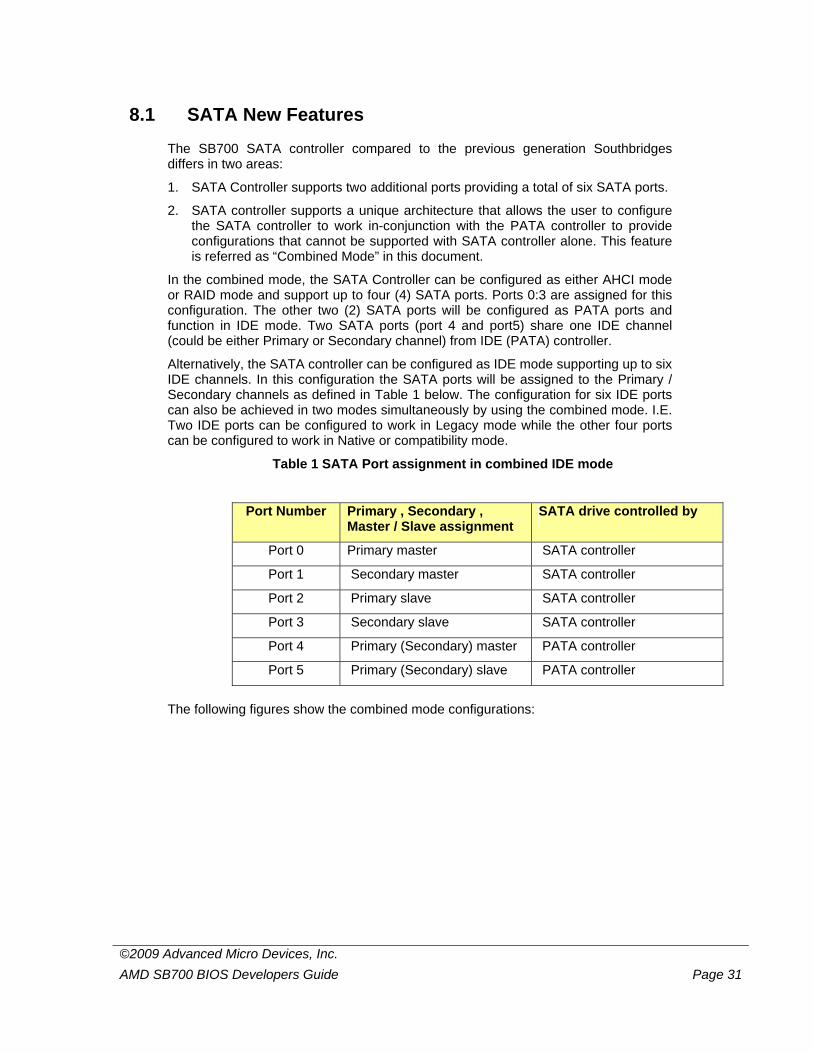
8.1 SATA New Features
The SB700 SATA controller compared to the previous generation Southbridges differs in two areas:
1. SATA Controller supports two additional ports providing a total of six SATA ports.
2. SATA controller supports a unique architecture that allows the user to configure the SATA controller to work in-conjunction with the PATA controller to provide configurations that cannot be supported with SATA controller alone. This feature is referred as “Combined Mode” in this document.
In the combined mode, the SATA Controller can be configured as either AHCI mode or RAID mode and support up to four (4) SATA ports. Ports 0:3 are assigned for this configuration. The other two (2) SATA ports will be configured as PATA ports and function in IDE mode. Two SATA ports (port 4 and port5) share one IDE channel (could be either Primary or Secondary channel) from IDE (PATA) controller.
Alternatively, the SATA controller can be configured as IDE mode supporting up to six IDE channels. In this configuration the SATA ports will be assigned to the Primary / Secondary channels as defined in Table 1 below. The configuration for six IDE ports can also be achieved in two modes simultaneously by using the combined mode. I.E. Two IDE ports can be configured to work in Legacy mode while the other four ports can be configured to work in Native or compatibility mode.
Table 1 SATA Port assignment in combined IDE mode
Port Number Primary , Secondary , Master / Slave assignment
SATA drive controlled by
Port 0 Primary master SATA controller
Port 1 Secondary master SATA controller
Port 2 Primary slave SATA controller
Port 3 Secondary slave SATA controller
Port 4 Primary (Secondary) master PATA controller
Port 5 Primary (Secondary) slave PATA controller
The following figures show the combined mode configurations:
©2009 Advanced Micro Devices, Inc. AMD SB700 BIOS Developers Guide Page 32
SATA controller in AHCI mode /
Combined modeP0
P1
P2
P3
P4
P5
PATA Controller
PATA Ide/atapi device
SATA device
SATA device
SATA device
SATA device
SATA device
SATA device
Port 4 and Port 5 operate in IDE mode. Configured as
IDE mode Primary or Secondary channel.
(selectable)
Hardware configuration view
PATA Controller
PATA Ide/atapi device
PATA Ide/atapi device
IDE Driver
MS inbox driver
SATA controller in AHCI mode /
Combined modeP0
P1
P2
P3
SATA device
SATA device
SATA device
SATA device
SATA drivers
Vista inbox AHCI or AMD RAID /
AHCI driver
Software view AHCI combined mode
Note: In this mode the MS inbox driver will control all PATA drives showing all devices under two physical IDE controllers.
Fig 4: Combined Mode Configurations
©2009 Advanced Micro Devices, Inc. AMD SB700 BIOS Developers Guide Page 33
8.2 Device ID
The SB700 SATA will have different device IDs for different drivers, because they are totally different devices from driver point of view. It’s not sufficient for OS to know whether to load IDE, AHCI, or RAID driver. In non fresh installed condition, Windows will match 4 IDs (vendor ID, device ID, sub-system ID, sub-vendor ID) first, and if they are matched, it will load the driver. Window will not check sub-class code if 4-IDs are matched. This will cause blue screen WinXP when SATA RAID driver loaded, and SATA controller is in IDE mode, if device ID is shared.
Device ID Device
4390 SATA in IDE mode
4391 SATA in AHCI mode with MS driver
4392 SATA in RAID mode with Promise non-Raid 5 driver
4393 SATA in RAID mode with Promise Raid5 driver
©2009 Advanced Micro Devices, Inc. AMD SB700 BIOS Developers Guide Page 34
8.3 SATA Controller Operating Modes
Whenever SATA is set to any IDE mode (native ide, legacy ide, ide->ahci, ide->hfs) and combined mode is set to OFF, only 4 ports (0-3) can be supported in SATA controller and other 2 ports (4-5) cannot be used (it may work under OS but will not work under BIOS). IDE->Hyperflash mode is intended only for driver testing and debugging. In IDE->Hyperflash mode, ports 1 & 3 will not work under BIOS post and this is limitation of hardware. When combined mode is ON, Ports 4/5 will always be connected through PATA controller, meaning any device connected to this port will be shown as PATA IDE device. For trevally reference board, SATA port 4 is the one which is closest to CPU and port 5 is the one which has mobile sata connector. For Shiner reference board ports 4, 5 are the two e-sata ports. Standalone mode was intended for debugging and bringup purposes only. Behind SATA mode will be the official driver supported mode and all qualification should be done in this mode.
8.4 SATA Hot Plug
The SATA hot plug feature is implemented through the following registers:
1. ACPI GPE0 Block status register bit 31 for SCI status.
2. ACPI GPE0 Block enable register bit 31 for SCI enable.
3. PMIO register 37h bit 2 to trigger SATA hot plug SCI.
1 = Rising edge.
0 = Falling edge trigger.
4. The SATA internal status is set whenever a SATA hard drive is plugged in, unplugged, powered up, or powered down. The status registers are:
Register BAR 5 + 10Ah, bit 0, for primary channel.
Register BAR 5 + 18Ah, bit 0, for secondary channel.
8.4.1 Sample Code
See section 14.7 for the SATA Hot Plug sample code.
©2009 Advanced Micro Devices, Inc. AMD SB700 BIOS Developers Guide Page 35
9 Power Management
On the SB700, PM registers can be accessed through I/O ports CD6h/CD7h. Before initiating any power management functions in the SB700, the BIOS needs to set the I/O base addresses for the ACPI I/O register, the SMI Command Port, and the SpeedStep Control register (etc):
I/O Name Description Configure Register Range Size (Bytes)
PM1_EVT ACPI PM1a_EVT_BLK PM IO Reg20h & Reg21h 4 PM1_CNT ACPI PM1a_CNT_BLK PM IO Reg22h & Reg23h 2 PM_TMR ACPI PM_TMR_BLK PM IO Reg24h & Reg25h 4 P_BLK ACPI P_BLK PM IO Reg26h & Reg27h 6 GPE0_EVT ACPI GPE0_EVT_BLK PM IO Reg28h & Reg29h 8 SMI CMD Block * SMI Command Block PM IO Reg2Ah & Reg2Bh 2
Notes:
• The SMI CMD Block must be word aligned, i.e., the least significant bit of the address must be zero (address[0] must be 0). For example, B0h, B2h, B4h, B6h, B8h etc.
• The SMI CMD Block consists of two ports – the SMI Command Port at base address, and the SMI Status Port at base address+1.
• The writes to the SMI Status Port will not generate an SMI. The writes to the SMI Command Port will generate an SMI.
• The SMI Command and SMI Status ports may be written individually as 8 bit ports, or together as a 16 bit port.
9.1 SMI Handling – EOS (PM IO Reg10h[Bit0])
Upon each SMI generation, the SB700 will clear the EOS bit automatically. At the end of the SMI service, the BIOS needs to clear the status bit of the SMI event and re-enable the EOS; otherwise, the SB700 will not be able to generate SMI, even if SMI events arrive.
9.2 Programmable I/Os
There are eight sets of programmable I/Os available on the SB700. The BIOS can use them for I/O trapping, which means that an SMI will be generated if any access falls into the PIO range.
The PIO address range can be set to 2, 4, 8, and 16.
I/O Name Description Configure Register Enable Status PIO0 Programmable I/O Range 0 PM IO Reg14h & Reg15h PM IO Reg1Ch[Bit7] PM IO Reg1Dh[Bit7]
PIO1 Programmable I/O Range 1 PM IO Reg16h & Reg17h PM IO Reg1Ch[Bit6] PM IO Reg1Dh[Bit6]
PIO2 Programmable I/O Range 2 PM IO Reg18h & Reg19h PM IO Reg1Ch[Bit5] PM IO Reg1Dh[Bit5]
PIO3 Programmable I/O Range 3 PM IO Reg1Ah & Reg1Bh PM IO Reg1Ch[Bit4] PM IO Reg1Dh[Bit4]
©2009 Advanced Micro Devices, Inc. AMD SB700 BIOS Developers Guide Page 36
I/O Name Description Configure Register Enable Status PIO4 Programmable I/O Range 4 PM IO RegA0 & RegA1h PM IO Reg A8h[Bit0] PM IO RegA9h[Bit0]
PIO5 Programmable I/O Range 5 PM IO RegA2 & RegA3h PM IO Reg A8h[Bit1] PM IO RegA9h[Bit1]
PIO6 Programmable I/O Range 6 PM IO RegA4 & RegA5h PM IO Reg A8h[Bit2] PM IO RegA9h[Bit2]
PIO7 Programmable I/O Range 7 PM IO RegA6 & RegA7h PM IO Reg A8h[Bit3] PM IO RegA9h[Bit3]
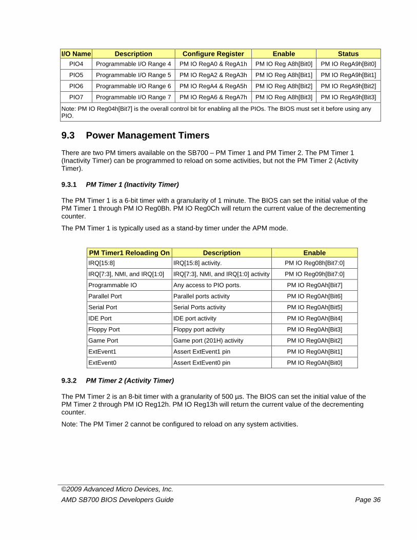
Note: PM IO Reg04h[Bit7] is the overall control bit for enabling all the PIOs. The BIOS must set it before using any PIO.
9.3 Power Management Timers
There are two PM timers available on the SB700 – PM Timer 1 and PM Timer 2. The PM Timer 1 (Inactivity Timer) can be programmed to reload on some activities, but not the PM Timer 2 (Activity Timer).
9.3.1 PM Timer 1 (Inactivity Timer)
The PM Timer 1 is a 6-bit timer with a granularity of 1 minute. The BIOS can set the initial value of the PM Timer 1 through PM IO Reg0Bh. PM IO Reg0Ch will return the current value of the decrementing counter.
The PM Timer 1 is typically used as a stand-by timer under the APM mode.
PM Timer1 Reloading On Description Enable IRQ[15:8] IRQ[15:8] activity. PM IO Reg08h[Bit7:0]
IRQ[7:3], NMI, and IRQ[1:0] IRQ[7:3], NMI, and IRQ[1:0] activity PM IO Reg09h[Bit7:0]
Programmable IO Any access to PIO ports. PM IO Reg0Ah[Bit7]
Parallel Port Parallel ports activity PM IO Reg0Ah[Bit6]
Serial Port Serial Ports activity PM IO Reg0Ah[Bit5]
IDE Port IDE port activity PM IO Reg0Ah[Bit4]
Floppy Port Floppy port activity PM IO Reg0Ah[Bit3]
Game Port Game port (201H) activity PM IO Reg0Ah[Bit2]
ExtEvent1 Assert ExtEvent1 pin PM IO Reg0Ah[Bit1]
ExtEvent0 Assert ExtEvent0 pin PM IO Reg0Ah[Bit0]
9.3.2 PM Timer 2 (Activity Timer)
The PM Timer 2 is an 8-bit timer with a granularity of 500 µs. The BIOS can set the initial value of the PM Timer 2 through PM IO Reg12h. PM IO Reg13h will return the current value of the decrementing counter.
Note: The PM Timer 2 cannot be configured to reload on any system activities.
©2009 Advanced Micro Devices, Inc. AMD SB700 BIOS Developers Guide Page 37
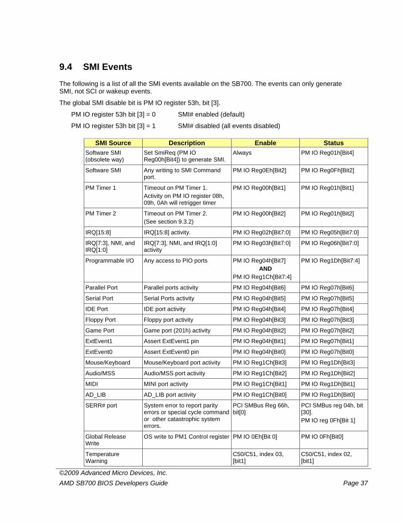
9.4 SMI Events
The following is a list of all the SMI events available on the SB700. The events can only generate SMI, not SCI or wakeup events.
The global SMI disable bit is PM IO register 53h, bit [3].
PM IO register 53h bit [3] = 0 SMI# enabled (default)
PM IO register 53h bit [3] = 1 SMI# disabled (all events disabled)
SMI Source Description Enable Status Software SMI (obsolete way)
Set SmiReq (PM IO Reg00h[Bit4]) to generate SMI.
Always PM IO Reg01h[Bit4]
Software SMI Any writing to SMI Command port.
PM IO Reg0Eh[Bit2] PM IO Reg0Fh[Bit2]
PM Timer 1 Timeout on PM Timer 1. Activity on PM IO register 08h, 09h, 0Ah will retrigger timer
PM IO Reg00h[Bit1] PM IO Reg01h[Bit1]
PM Timer 2 Timeout on PM Timer 2. (See section 9.3.2)
PM IO Reg00h[Bit2] PM IO Reg01h[Bit2]
IRQ[15:8] IRQ[15:8] activity. PM IO Reg02h[Bit7:0] PM IO Reg05h[Bit7:0]
IRQ[7:3], NMI, and IRQ[1:0]
IRQ[7:3], NMI, and IRQ[1:0] activity
PM IO Reg03h[Bit7:0] PM IO Reg06h[Bit7:0]
Programmable I/O Any access to PIO ports PM IO Reg04h[Bit7] AND
PM IO Reg1Ch[Bit7:4]
PM IO Reg1Dh[Bit7:4]
Parallel Port Parallel ports activity PM IO Reg04h[Bit6] PM IO Reg07h[Bit6]
Serial Port Serial Ports activity PM IO Reg04h[Bit5] PM IO Reg07h[Bit5]
IDE Port IDE port activity PM IO Reg04h[Bit4] PM IO Reg07h[Bit4]
Floppy Port Floppy port activity PM IO Reg04h[Bit3] PM IO Reg07h[Bit3]
Game Port Game port (201h) activity PM IO Reg04h[Bit2] PM IO Reg07h[Bit2]
ExtEvent1 Assert ExtEvent1 pin PM IO Reg04h[Bit1] PM IO Reg07h[Bit1]
ExtEvent0 Assert ExtEvent0 pin PM IO Reg04h[Bit0] PM IO Reg07h[Bit0]
Mouse/Keyboard Mouse/Keyboard port activity PM IO Reg1Ch[Bit3] PM IO Reg1Dh[Bit3]
Audio/MSS Audio/MSS port activity PM IO Reg1Ch[Bit2] PM IO Reg1Dh[Bit2]
MIDI MINI port activity PM IO Reg1Ch[Bit1] PM IO Reg1Dh[Bit1]
AD_LIB AD_LIB port activity PM IO Reg1Ch[Bit0] PM IO Reg1Dh[Bit0]
SERR# port System error to report parity errors or special cycle command or other catastrophic system errors.
PCI SMBus Reg 66h, bit[0]
PCI SMBus reg 04h, bit [30]. PM IO reg 0Fh[Bit 1]
Global Release Write
OS write to PM1 Control register PM IO 0Eh[Bit 0] PM IO 0Fh[Bit0]
Temperature Warning
C50/C51, index 03, [bit1]
C50/C51, index 02, [bit1]
©2009 Advanced Micro Devices, Inc. AMD SB700 BIOS Developers Guide Page 38
9.4.1 Power Button
Power button is always a wake-up event and can be programmed as an SCI wake-up event. The power button status register is AcpiPmEvtBlk, bit[8]. The BIOS must make sure this bit is cleared prior to the entry into any C or S states.
In addition, when the power button is pressed for 4 seconds, the SB700 will shut down the entire system (by going to S5). No programming is required for this function.
9.5 C-State Break Events
9.5.1 Break Events for C2 State
Under C2 the break events are as follows:
• PBE#
• Special_message from CPU (K8 mode)
• I/O write to special register (K8 mode)
• SMI#
• NMI
• INIT
• Interrupts (in PIC mode only)
9.5.2 Break Events for C3 and C4 States
All of the events listed (above) as break events in C2 state are also break events in C3 and C4 states. In addition, the Bus Master Status is also a break event in C3 and C4 states.
9.6 Save/Restore Sequence for S3 State
9.6.1 Register Save Sequence for S3 State
Prior to initiating S3 states, the BIOS must save the registers on the machine. The BIOS reserves a section of the memory and a section of the CMOS to save the registers. Depending on the BIOS architecture, these registers may be saved either one time just prior to handing of the control over to the OS, or every time just before going into the S3 states.
The following registers must be saved:
• Some Northbridge registers in CMOS
• Some Northbridge and Memory Controller registers
• Southbridge PCI registers on the SB700
• Southbridge non-PCI registers
• PCI registers not on the SB700
• Super I/O and other I/O registers.
©2009 Advanced Micro Devices, Inc. AMD SB700 BIOS Developers Guide Page 39
The BIOS typically sets aside an area in the memory to save the registers prior to the S3 state. The Southbridge registers may be saved in any order as long as those registers are visible to the BIOS.
Some of the registers, such as SubSystem ID and SubSystem Vendor ID, may be saved, but written only once as dword. They are handled separately during restore.
9.7 Wake on Events
TBD
9.8 Sleep SMI Events
These events provide an SMI# before the system transits to an SX state (e.g. ACPI S1, S2, S3, S4, and S5). This feature helps the System BIOS to develop software workarounds or debugging routines before the system goes to sleep state.
9.8.1 Sleep SMI Control Register
There is a Sleep SMI control register in the SB700. Its base I/O address is defined at PMIO Reg 0x04.
SLP_SMI_EN is a R/W register bit for controlling a Sleep SMI when the system transits to an ACPI SX state. The register definition is as follows:
• SLP_SMI_EN [Bit7] = 0, Disables Sleep SMI event.
• SLP_SMI_EN [Bit7] = 1, Enables Sleep SMI event. There is a Sleep SMI Status register in the SB700. Its base I/O address is defined at PMIO Reg 0x07.
SLP_SMI_Status [Bit7] is asserted when the system goes to an ACPI SX state, and when SLP_SMI_EN is set to enable.
9.8.2 Sleep SMI Programming Sequence
9.8.2.1 Set Sleep SMI Control Register
The Sleep SMI Control Register does not necessary have to be enabled before the system goes to the ACPI SX state. One may enable the control the bit in the ACPI ASL code. Please refer to section 14.9 “Sleep Trap Through SMI#” for the sample code.
9.8.2.2 Enter Sleep SMI# Routine
The system does not go into the sleep state (set by ACPI PM1_CNT) when SMI# is asserted. The System BIOS has to follow the sequence below:
1. Disable Sleep SMI Control register (SLP_SMI_EN). 2. Software workaround or system BIOS debugging routing implementation. 3. Write SLP_SMI_Status 1 to clear this event. 4. Rewrite sleep command to ACPI register (ACPI PM1_CNT). 5. RSM if necessary.
©2009 Advanced Micro Devices, Inc. AMD SB700 BIOS Developers Guide Page 40
10 APIC Programming
With the AMD integrated chipset solution, the BIOS needs to program both the Northbridge and the Southbridge in order to support APIC.
10.1 Northbridge APIC Enable
There are three bits in the Northbridge that the BIOS should set before enabling APIC support.
For RS480/RS690:
• Enable Local APIC in K8. (Set bit11 in APIC_BASE MSR(001B) register.) • Reg4C[bit1] - This bit should be set to enable. It forces the CPU request with address
0xFECx_xxxx to the Southbridge. • Reg4C[bit18] - This bit should be set to enable. It sets the Northbridge to accept MSI
with address 0xFEEx_xxxx from the Southbridge.
10.2 Southbridge APIC Enable
There are two bits in the Southbridge that the BIOS should set before enabling APIC support.
• Reg64[bit3] = 1 to enable the APIC function. • Reg64[bit7] = 1 to enable the xAPIC function. It is only valid if Bit3 is being set.
10.3 IOAPIC Base Address
The IOAPIC base address can be defined at SMBus PCI Reg. 74h. The power-on default value is FEC00000h.
Note: This register is 32-bit access only. The BIOS should not use the byte restore mechanism to restore its value during S3 resume.
10.4 APIC IRQ Assignment
SB700 has IRQ assignments under APIC mode as follows:
• IRQ0~15 – legacy IRQ • IRQ 16 – PCI INTA • IRQ 17 – PCI INTB • IRQ 18 – PCI INTC • IRQ 19 – PCI INTD • IRQ 20 – PCI INTE • IRQ 21 – PCI INTF • IRQ 22 – PCI INTG • INT 23 – PCI INTH • IRQ 09 – ACPI SCI
SCI is still as low-level trigger with APIC enabled.
©2009 Advanced Micro Devices, Inc. AMD SB700 BIOS Developers Guide Page 41
10.5 APIC IRQ Routing
During the BIOS POST, the BIOS will do normal PCI IRQ routing through port C00h/C01h. Once APIC is fully enabled by the OS, the routing in C00h/C01 must be all cleared to zero.
The following is a sample ASL code that may be incorporated into the BIOS:
Name(PICF,0x00) Method(_PIC, 0x01, NotSerialized) { Store (Arg0, PICF) If(Arg0) { \_SB.PCI0.LPC0.DSPI() // clear interrupt at 0xC00/0xC01 } } OperationRegion(PIRQ, SystemIO, 0xC00, 0x2) Field(PIRQ, ByteAcc, NoLock, Preserve) {
PIID, 8, PIDA, 8 } IndexField(PIID, PIDA, ByteAcc, NoLock, Preserve) {
PIRA, 8, PIRB, 8, PIRC, 8, PIRD, 8, PIRS, 8 Offset(0x09), PIRE, 8, PIRF, 8, PIRG, 8, PIRH, 8
} Method(DSPI) {
Store(0x00, PIRA) Store(0x00, PIRB) Store(0x00, PIRC) Store(0x00, PIRD) Store(0x00, PIRS) Store(0x00, PIRE) Store(0x00, PIRF) Store(0x00, PIRG) Store(0x00, PIRH)
}
©2009 Advanced Micro Devices, Inc. AMD SB700 BIOS Developers Guide Page 42
11 Watchdog Timer
To enable the watchdog timer in the SB700, the following registers must be initialized:
• Enable the watchdog timer by resetting bit 0 in PMIO register 069h. • Set bit 3 in SMBus PCI Config (Bus 0 Device 20 Function 0) Reg 41h to enable the
watchdog decode. • Ensure that the watchdog timer base address is set to a non zero value, typically
0FEC000F0h. The watchdog base address is set at PMIO address 6Ch-6Fh as shown in the sample program below. (PMIO is addressed as byte index/data):
Sample Program:
mov dx,0CD6h ; PMIO index register
mov al,6Fh ; Most significant base address location
out dx,al ; Set the index to 6Fh
mov dx,0CD7h ; PMIO data register
mov al,0FEh ; Most significant base address
out dx,al
mov dx,0CD6h ; PMIO index register
mov al,6Eh ; Second significant base address location
out dx,al ; Set the index to 6Eh
mov dx,0CD7h ; PMIO data register
mov al,0C0h ; Second significant base address
out dx,al
mov dx,0CD6h ; PMIO index register
mov al,6Dh ; Third significant base address location
out dx,al ; Set the index to 6Dh
mov dx,0CD7h ; PMIO data register
mov al,00h ; Third significant base address
out dx,al
mov dx,0CD6h ; PMIO index register
mov al,6Ch ; Least significant base address location
out dx,al ; Set the index to 6Ch
mov dx,0CD7h ; PMIO data register
mov al,0F0h ; Least significant base address
out dx,al

©2009 Advanced Micro Devices, Inc. AMD SB700 BIOS Developers Guide Page 43
To verify that the watchdog timer works correctly, perform the following steps:
• Write 100 (count) to the watchdog count register at address 0FEC000F4h. • Enable and start the watchdog timer by writing 00000081h to the watchdog control
register at 0FEC000F0h. • The counter will start decrementing and will reset the system once it reaches 0. This
means that the watchdog timer is working as designed.
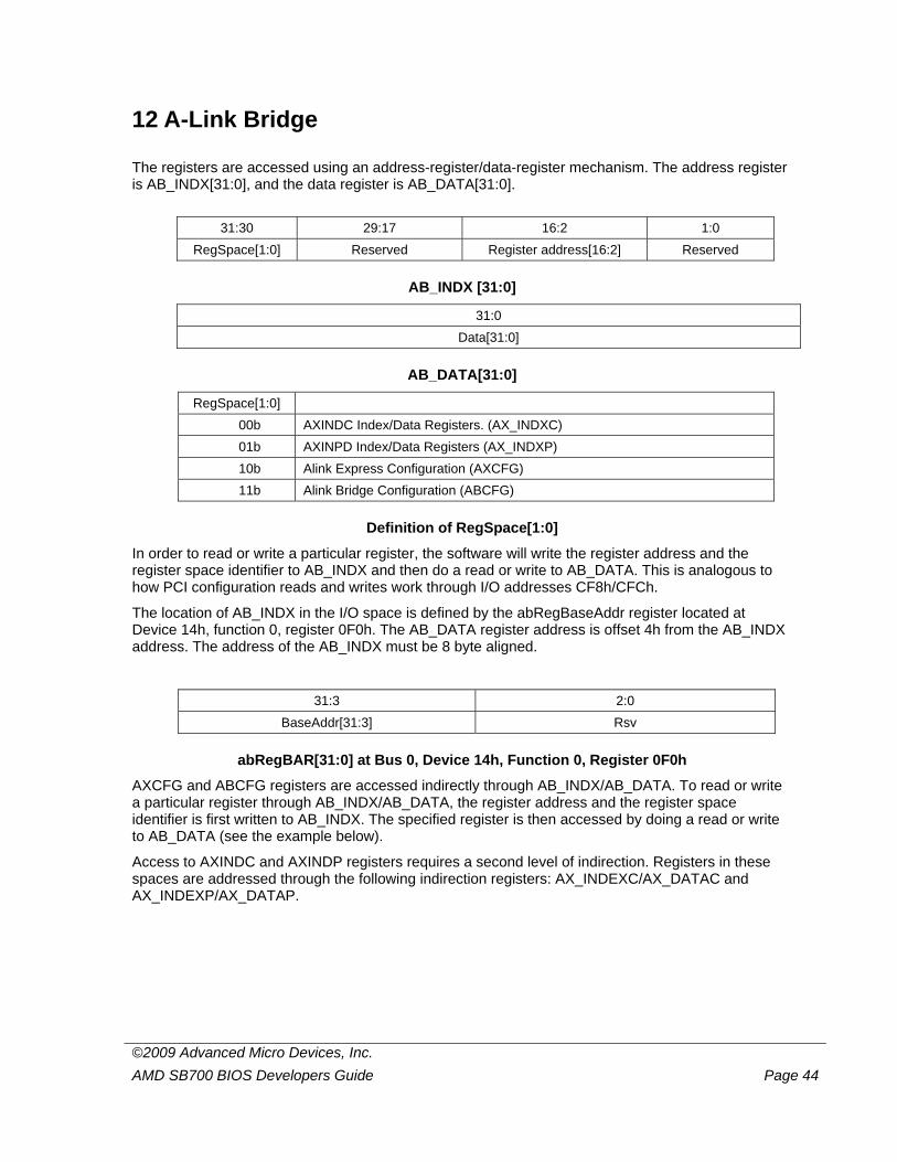
©2009 Advanced Micro Devices, Inc. AMD SB700 BIOS Developers Guide Page 44
12 A-Link Bridge
The registers are accessed using an address-register/data-register mechanism. The address register is AB_INDX[31:0], and the data register is AB_DATA[31:0].
31:30 29:17 16:2 1:0
RegSpace[1:0] Reserved Register address[16:2] Reserved
AB_INDX [31:0]
31:0 Data[31:0]
AB_DATA[31:0]
RegSpace[1:0] 00b AXINDC Index/Data Registers. (AX_INDXC) 01b AXINPD Index/Data Registers (AX_INDXP) 10b Alink Express Configuration (AXCFG) 11b Alink Bridge Configuration (ABCFG)
Definition of RegSpace[1:0]
In order to read or write a particular register, the software will write the register address and the register space identifier to AB_INDX and then do a read or write to AB_DATA. This is analogous to how PCI configuration reads and writes work through I/O addresses CF8h/CFCh.
The location of AB_INDX in the I/O space is defined by the abRegBaseAddr register located at Device 14h, function 0, register 0F0h. The AB_DATA register address is offset 4h from the AB_INDX address. The address of the AB_INDX must be 8 byte aligned.
31:3 2:0 BaseAddr[31:3] Rsv
abRegBAR[31:0] at Bus 0, Device 14h, Function 0, Register 0F0h
AXCFG and ABCFG registers are accessed indirectly through AB_INDX/AB_DATA. To read or write a particular register through AB_INDX/AB_DATA, the register address and the register space identifier is first written to AB_INDX. The specified register is then accessed by doing a read or write to AB_DATA (see the example below).
Access to AXINDC and AXINDP registers requires a second level of indirection. Registers in these spaces are addressed through the following indirection registers: AX_INDEXC/AX_DATAC and AX_INDEXP/AX_DATAP.
©2009 Advanced Micro Devices, Inc. AMD SB700 BIOS Developers Guide Page 45
Register Indirect Address
AX_INDXC 30h
AX_DATAC 34h
AX_INDXP 38h
AX_DATAP 3Ch
Example: To write to register 21h in the INDXC space with a data of 00, the following steps are required:
1. Out 30h to AB_INDX. This will prepare to write register from INDXC
2. Out 21h to AB_DATA. This will set register 21h of INDXC
3. Out 34h to AB_INDX. This will prepare to write data to register defined in steps 1 and 2 above
4. Out 00 to AB_DATA. This will write the data to the register defined n steps 1 and 2 above.
12.1 Programming Procedure
Indirect access is required to access both A-Link Express Configuration and A-Link Bridge Configuration register space. The programming procedure is as follows:
Write:
1. Set the A-Link bridge register access address. This address is set at device 14h, function 0, register 0F0h. This is an I/O address and needs to be set only once after power-up. The I/O address must be on a 8-byte boundary (i.e., 3 LS bits must be zeroes).
Example: To set C80h as an A-Link bridge register access address:
mov dx,0CF8h ; To access device 14h, function 0
mov eax,8000A0F0h ;
out dx,eax
mov dx,0CFCh
mov eax,00000C80h ; A-Link bridge register access address
out dx,eax
Note: Although the 32-bit I/O address is set for the A-Link bridge (e.g., 00000C80h), the bridge may be accessed by a 16-bit address (i.e., 0C80h). The MS word is set to 00 by default (see the example below).
2. Write the register address in the AB_INDX.
Example: To write to the A-Link Bridge configuration register space at 90h:
mov dx,0c80h ; I/O address index assigned to A-Link
mov eax, 0C0000090h ; Bits[31:30] = 11 for A-Link Bridge register ; space
©2009 Advanced Micro Devices, Inc. AMD SB700 BIOS Developers Guide Page 46
out dx,eax ; Register index is set
mov dx,0c84h ; I/O address for data
mov eax,00000001h ; Power down 2 lanes to save power
out dx,eax
Read:
Use a similar indirect procedure to read out the register value inside AB and BIF.
12.2 A-Link Express Configuration DMA Access
To enable A-Link Express Configuration DMA access, a specific register space needs to be configured first. This register is in the A-Link Express register space that refers to port-specific configuration registers (see section 12 above for a description of the AB_INDX register). When configuring the register, bit2 of byte 4 needs to be set to “1” to enable the DMA access.
Follow these steps to initialize A-Link Express configuration DMA access (this initialization has to be performed during S3 wakeup also):
1. Issue an I/O write to AB_INDX. The write data's bit [31:30] should be 10 b(binary). The register to be written is in the port-specific configuration register space, and bit [16:0] should be 0x4 (hex).
2. Issue an I/O write to AB_Data. This write data's bits[31:0] should be 0x4h (i.e., 32'b0000_0000_0000_0100 binary).
mov dx, _0C80h ; ALINK_ACCESS_INDEX
in eax, dx
and eax, NOT (0C001FFFFh)
or eax, 080000004h
out dx, eax
mov dx, 0C84h ; ALINK_ACCESS_DATA
mov eax, 04h
out dx, eax
;Write AB_INDX 0x30
;Write AB_DATA 0x21
;Write AB_INDX 0x34
;Write AB_DATA 0x00
mov dx, 0C80h ; ALINK_ACCESS_INDEX
mov eax, 30h
out dx, eax
mov dx, 0C84h ; ALINK_ACCESS_DATA
mov eax, 21h
out dx, eax
mov dx,0C80h ; ALINK_ACCESS_INDEX
©2009 Advanced Micro Devices, Inc. AMD SB700 BIOS Developers Guide Page 47
mov eax, 34h
out dx, eax
mov dx, 0C84h ; ALINK_ACCESS_DATA
mov eax, 00h
out dx, eax
12.3 Enable Non-Posted Memory Write for K8 Platform.
The register index 10h of AXINDC bit9 should be set to 1.
mov dx,AB_INDX ; AB index register
mov eax,30h ; Address of AXINDC
out dx,eax ; Set register address
mov dx,AB_DATA ; To write register address
mov eax,10h ; Write register address
out dx,eax
mov dx,AB_INDX
mov eax,34h ; To write data portion of the AXINDC
out dx,eax
mov dx,AB_DATA
in eax,dx ; Read the current data
or al,200h ; Set bit 9
out dx,eax ; Write data back.
©2009 Advanced Micro Devices, Inc. AMD SB700 BIOS Developers Guide Page 48
13 High Precision Event Timer (HPET)
The SB700 includes an industry standard High Precision Event Timers (HPET). The details and the operation of the timer are described in the IA-PC HPET specification. This section describes the timer initialization in the SB700 chipset.
13.1 Initialization
For SB700 is HPET usage is required, then during the early POST, the timer base address must be programmed in Device 14h, Function 0, register 14h. This base address is also reported to the operating system through the ACPI table as specified in the specification. In addition, the HPET interrupts may also be enabled through Device 14h, Function 0, register 64h, bit 10.
13.1.1 Sample Initialization Code
HpetBaseAddress EQU 0FED00000H ; OEM specific address ; Set Base address in Device 14h, Function 0, Register 14h mov dx,0CF8h ; PCI index register mov eax,8000A014h ; Bus 0, Device 14h, Function 0, Register 14h out dx,eax ; Set PCI index to register 14h mov dx,0CFCh ; PCI data register mov eax,0FED00000h ; Base address, OEM specific out dx,eax ; Enable the HPET interrupts, if needed. Set Device 14h, Function 0, Register 64h, bit 10 mov dx,0CF8h ; PCI index register mov eax,8000A064h ; Bus 0, Device 14h, Function 0, Register 64h out dx,eax ; Set PCI index to register 64h mov dx,0CFCh ; PCI data register in eax,dx ; Read current value of register 64h or eax,00000400h ; Set bit 10 out dx,eax
©2009 Advanced Micro Devices, Inc. AMD SB700 BIOS Developers Guide Page 49
13.2 ACPI HPET Description Table
As described in the specification, an ACPI HPET table is required to report the base address to the operating system. The table includes a ACPI table header, and HPET table-specific fields. The sample values for the HPET specific fields are as follows: Event Timer Block ID DD 00000000h Base Address (Lower 4 bytes) DD 00000800h Base Address (Middle 4 bytes) DD 0FED00000h ; Address on 32 bit system Base Address (Upper 4 bytes) DD 00000000h ; Used on 64 bit system HPET Number DB 00h Minimum Clock Tick DW 37EEh ; 14318 (decimal)
13.3 HPET Support for Vista
For the SB700, PM_IO register 72h bits [2:0] should be set to 111b for Longhorn support.
©2009 Advanced Micro Devices, Inc. AMD SB700 BIOS Developers Guide Page 50
14 Sample Programs
14.1 IXP700 Register Initialization on Power-Up
14.1.1 Initialization of PCI IRQ Routing before Resource Allocation
The PCI IRQs are programmed using index/data format through registers C00h/C01h. Index 0 through 3, and 9 through 0Ch, are for PCI IRQ lines. Index 4 is for SCI interrupt generated for ACPI, and Index 5 is for SMBus interrupt. Sample Program The following routine initializes all PCI interrupts to zeroes. PciIrqInit proc near
push ax ; Save the registers used in the routine
push dx
mov ax,00h ; Start with index = 0, data = 0
ClearPciIrq0To5:
mov dx,0C00h ; PCI interrupt index port
out dx,al ; Set index
mov dx,0C01h ; PCI interrupt data port
xchg ah,al ; Get data in AL = 0
out dx,al
xchg ah,al ; AL = Index
inc al ; Point to next index
cmp al, 05h ; Max index in 0 to 5 series
jbe ClearPciIrq0To5
; Initialize for index 9 through 0Ch
mov ax,0009h ; To clear from index 09 to 0Ch
ClearPciIrq9ToC:
mov dx,0C00h ; PCI interrupt index port
out dx,al ; Set index
mov dx,0C01h ; PCI interrupt data port
xchg ah,al ; Get data in AL = 0
out dx,al
xchg ah,al ; AL = Index
inc al ; Point to next index
cmp al, 0Ch ; Max index in 9 to 0Ch series
jbe ClearPciIrq9ToC
pop dx ; Restore the registers
©2009 Advanced Micro Devices, Inc. AMD SB700 BIOS Developers Guide Page 51
pop ax
ret
PciIrqInit endp
14.2 Setup Options
14.2.1 64 Bytes DMA
If 64 bytes DMA is selected for P2P bridge, set PCI to PCI bridge device 14h, function 4, register 4Bh, bit 4 to 1.
14.2.2 USB Overcurrent Detection Disable
To disable over-current detection for both OHCI and EHCI USB devices, set USB device 13h, function 0 register 51h, bit 0.
Sample Program
UsbOverCurrentDetectionDisable proc near
push eax ; Save registers used by this device
push dx
mov dx,0CF8h ; PCI configuration space index register
mov eax,8000A850h ; Device 13h, function 0, register 50h-53h
out dx,eax
mov dx,0CFDh ; PCI configuration space. Access reg. 51h
in dx,al ; Read current value
or al,01h ; Set to disable USB OHCI and EHCI overcurrent
out dx,al
pop dx ; Restore registers used by this routine
pop eax
ret
UsbOverCurrentDetectionDisable endp
14.2.3 C3 Support
The C3 support depends on the processor PBE support and HyperThreading. The ACPI FACP table also needs to be modified for C3 support. The description below applies only to the SB700 registers affected by C3 support.
PM I/O register 51h is set to C3 latency as follows:
C3 Latency = (bits[5:0] of PM I/O register 51h) * 8us
Hence for recommended C3 Latency = 40us, set (bits[5:0] of PM I/O register 51h) = 5
©2009 Advanced Micro Devices, Inc. AMD SB700 BIOS Developers Guide Page 52
For deep C3 support, in addition to setting register 51h above, PM I/O register 50h bit0 must also be set to 1.
14.2.4 Subtractive Decoding for P2P Bridge
To enable the subtractive decoding, set device 14h, function 4, P2P bridge register 40h bit 5 to 1.
Sample Program:
EnableSubtractiveDecoding proc near
push eax ; Save registers used in this routine
push dx
mov dx,0CF8h
mov eax,8000A440h ; Bus 0, device 14h, function 4, register 40h, P2P
out dx,eax
mov dx,0CFCh ; To access register 40h
in al,dx
or al,20h ; Set bit 5 for subtractive decoding
out dx,al
; Set bit 7 of register 4Bh to show subtractive decoding in class code reg. 09h bit 0
mov dx,0CF8h
mov eax,8000A448h ; Bus 0, device 14h, function 4, register 48h-4Bh
out dx,eax
mov dx,0CFFh ; To access register 4Bh
in al,dx
or al,80h ; Control bit for PI register
out dx,al
pop dx ; Restore registers
pop eax
ret
EnableSubtractiveDecoding endp
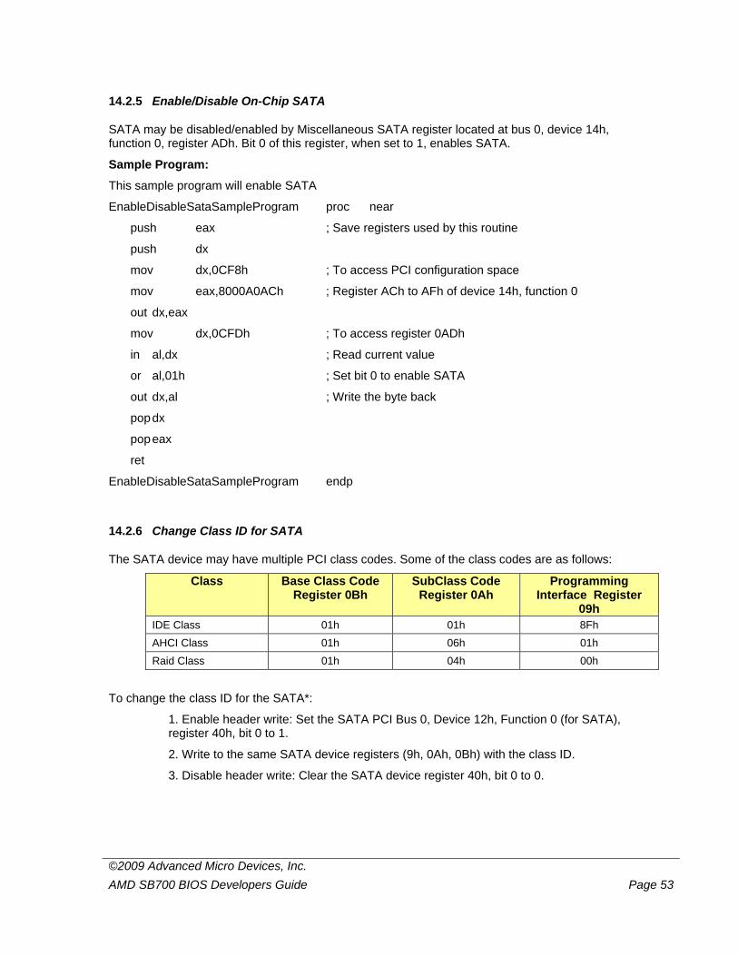
©2009 Advanced Micro Devices, Inc. AMD SB700 BIOS Developers Guide Page 53
14.2.5 Enable/Disable On-Chip SATA
SATA may be disabled/enabled by Miscellaneous SATA register located at bus 0, device 14h, function 0, register ADh. Bit 0 of this register, when set to 1, enables SATA.
Sample Program:
This sample program will enable SATA
EnableDisableSataSampleProgram proc near
push eax ; Save registers used by this routine
push dx
mov dx,0CF8h ; To access PCI configuration space
mov eax,8000A0ACh ; Register ACh to AFh of device 14h, function 0
out dx,eax
mov dx,0CFDh ; To access register 0ADh
in al,dx ; Read current value
or al,01h ; Set bit 0 to enable SATA
out dx,al ; Write the byte back
pop dx
pop eax
ret
EnableDisableSataSampleProgram endp
14.2.6 Change Class ID for SATA
The SATA device may have multiple PCI class codes. Some of the class codes are as follows:
Class Base Class Code Register 0Bh
SubClass Code Register 0Ah
Programming Interface Register
09h IDE Class 01h 01h 8Fh AHCI Class 01h 06h 01h Raid Class 01h 04h 00h
To change the class ID for the SATA*:
1. Enable header write: Set the SATA PCI Bus 0, Device 12h, Function 0 (for SATA), register 40h, bit 0 to 1.
2. Write to the same SATA device registers (9h, 0Ah, 0Bh) with the class ID.
3. Disable header write: Clear the SATA device register 40h, bit 0 to 0.
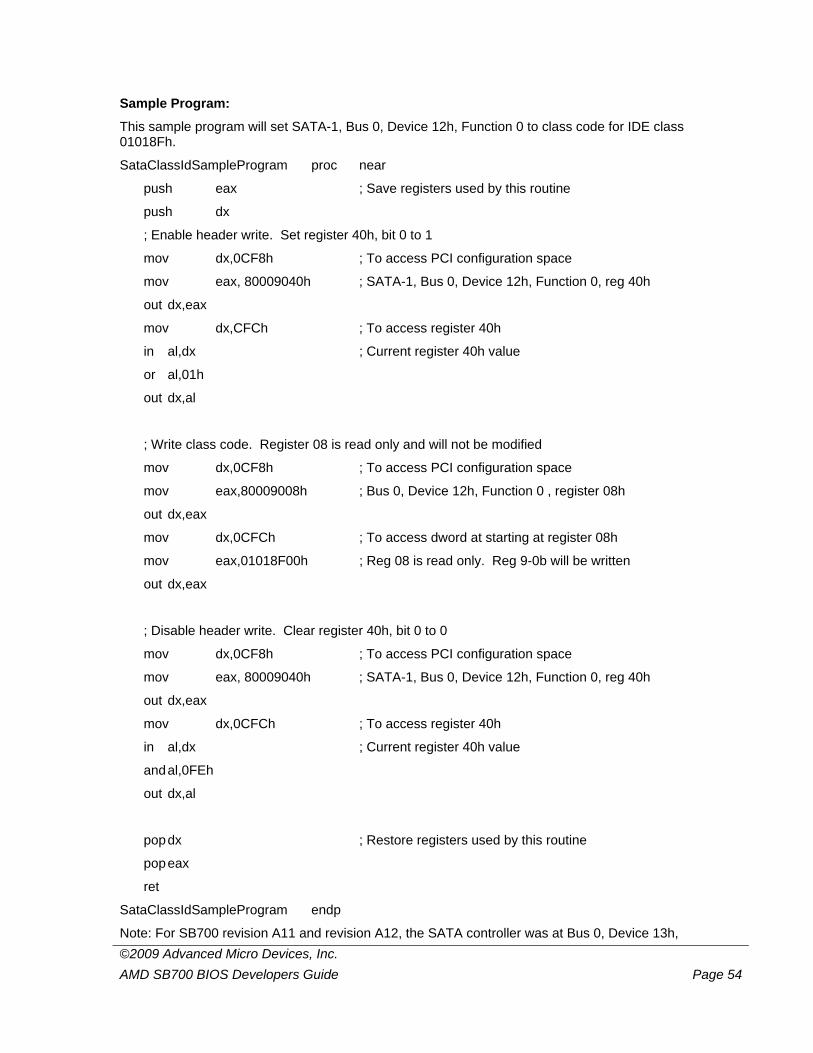
©2009 Advanced Micro Devices, Inc. AMD SB700 BIOS Developers Guide Page 54
Sample Program:
This sample program will set SATA-1, Bus 0, Device 12h, Function 0 to class code for IDE class 01018Fh.
SataClassIdSampleProgram proc near
push eax ; Save registers used by this routine
push dx
; Enable header write. Set register 40h, bit 0 to 1
mov dx,0CF8h ; To access PCI configuration space
mov eax, 80009040h ; SATA-1, Bus 0, Device 12h, Function 0, reg 40h
out dx,eax
mov dx,CFCh ; To access register 40h
in al,dx ; Current register 40h value
or al,01h
out dx,al
; Write class code. Register 08 is read only and will not be modified
mov dx,0CF8h ; To access PCI configuration space
mov eax,80009008h ; Bus 0, Device 12h, Function 0 , register 08h
out dx,eax
mov dx,0CFCh ; To access dword at starting at register 08h
mov eax,01018F00h ; Reg 08 is read only. Reg 9-0b will be written
out dx,eax
; Disable header write. Clear register 40h, bit 0 to 0
mov dx,0CF8h ; To access PCI configuration space
mov eax, 80009040h ; SATA-1, Bus 0, Device 12h, Function 0, reg 40h
out dx,eax
mov dx,0CFCh ; To access register 40h
in al,dx ; Current register 40h value
and al,0FEh
out dx,al
pop dx ; Restore registers used by this routine
pop eax
ret
SataClassIdSampleProgram endp
Note: For SB700 revision A11 and revision A12, the SATA controller was at Bus 0, Device 13h,
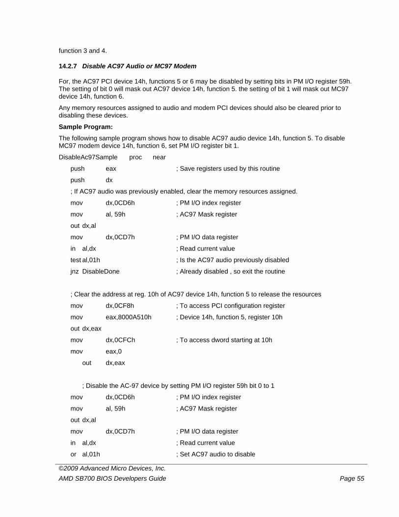
©2009 Advanced Micro Devices, Inc. AMD SB700 BIOS Developers Guide Page 55
function 3 and 4.
14.2.7 Disable AC97 Audio or MC97 Modem
For, the AC97 PCI device 14h, functions 5 or 6 may be disabled by setting bits in PM I/O register 59h. The setting of bit 0 will mask out AC97 device 14h, function 5. the setting of bit 1 will mask out MC97 device 14h, function 6.
Any memory resources assigned to audio and modem PCI devices should also be cleared prior to disabling these devices.
Sample Program:
The following sample program shows how to disable AC97 audio device 14h, function 5. To disable MC97 modem device 14h, function 6, set PM I/O register bit 1.
DisableAc97Sample proc near
push eax ; Save registers used by this routine
push dx
; If AC97 audio was previously enabled, clear the memory resources assigned.
mov dx,0CD6h ; PM I/O index register
mov al, 59h ; AC97 Mask register
out dx,al
mov dx,0CD7h ; PM I/O data register
in al,dx ; Read current value
test al,01h ; Is the AC97 audio previously disabled
jnz DisableDone ; Already disabled , so exit the routine
; Clear the address at reg. 10h of AC97 device 14h, function 5 to release the resources
mov dx,0CF8h ; To access PCI configuration register
mov eax,8000A510h ; Device 14h, function 5, register 10h
out dx,eax
mov dx,0CFCh ; To access dword starting at 10h
mov eax,0
out dx,eax
; Disable the AC-97 device by setting PM I/O register 59h bit 0 to 1
mov dx,0CD6h ; PM I/O index register
mov al, 59h ; AC97 Mask register
out dx,al
mov dx,0CD7h ; PM I/O data register
in al,dx ; Read current value
or al,01h ; Set AC97 audio to disable
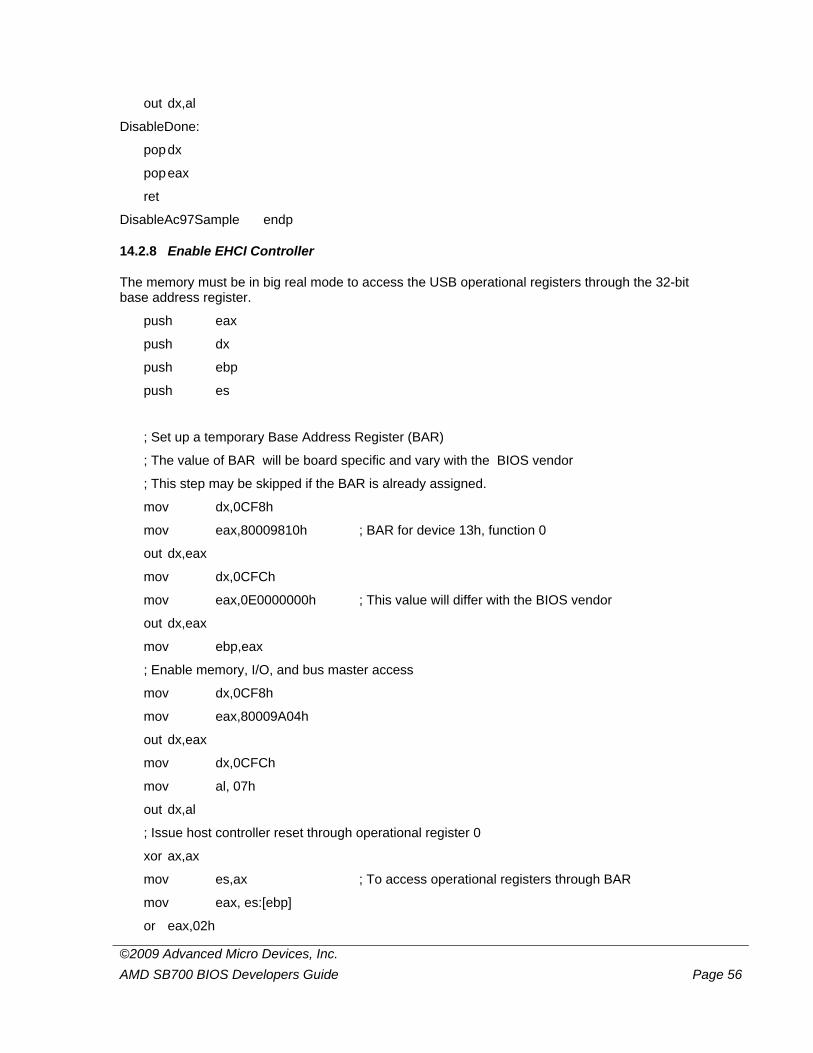
©2009 Advanced Micro Devices, Inc. AMD SB700 BIOS Developers Guide Page 56
out dx,al
DisableDone:
pop dx
pop eax
ret
DisableAc97Sample endp
14.2.8 Enable EHCI Controller
The memory must be in big real mode to access the USB operational registers through the 32-bit base address register.
push eax
push dx
push ebp
push es
; Set up a temporary Base Address Register (BAR)
; The value of BAR will be board specific and vary with the BIOS vendor
; This step may be skipped if the BAR is already assigned.
mov dx,0CF8h
mov eax,80009810h ; BAR for device 13h, function 0
out dx,eax
mov dx,0CFCh
mov eax,0E0000000h ; This value will differ with the BIOS vendor
out dx,eax
mov ebp,eax
; Enable memory, I/O, and bus master access
mov dx,0CF8h
mov eax,80009A04h
out dx,eax
mov dx,0CFCh
mov al, 07h
out dx,al
; Issue host controller reset through operational register 0
xor ax,ax
mov es,ax ; To access operational registers through BAR
mov eax, es:[ebp]
or eax,02h
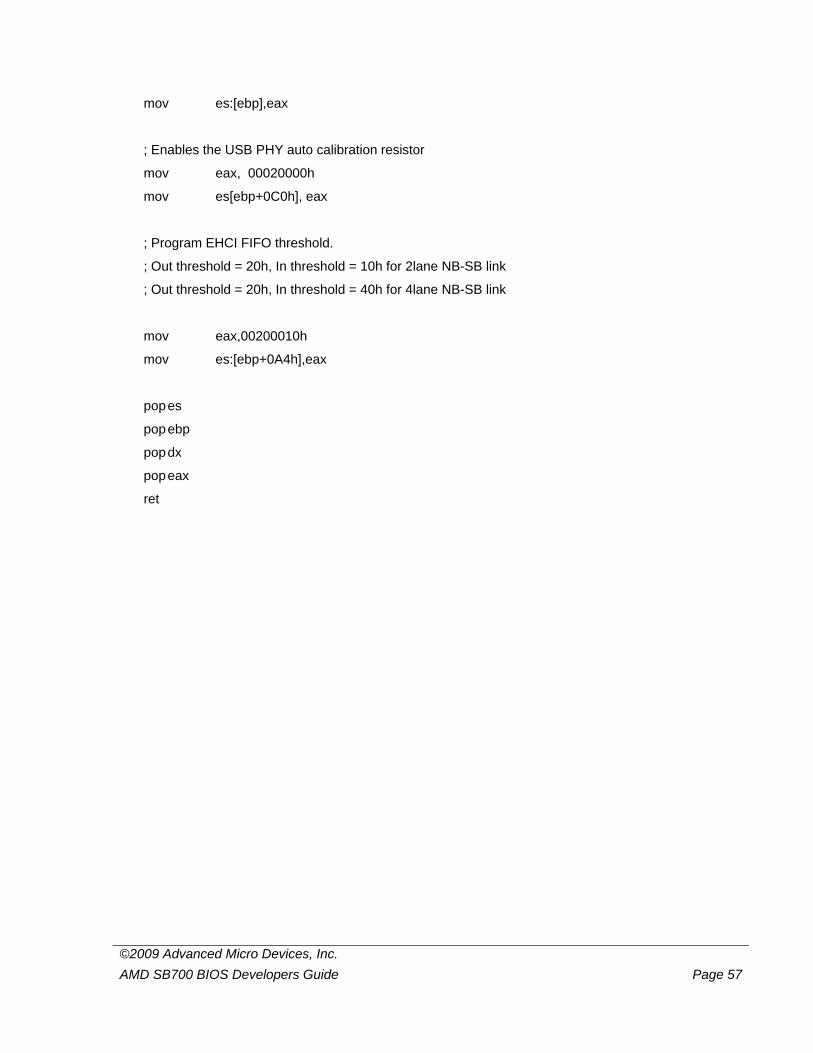
©2009 Advanced Micro Devices, Inc. AMD SB700 BIOS Developers Guide Page 57
mov es:[ebp],eax
; Enables the USB PHY auto calibration resistor
mov eax, 00020000h
mov es[ebp+0C0h], eax
; Program EHCI FIFO threshold.
; Out threshold = 20h, In threshold = 10h for 2lane NB-SB link
; Out threshold = 20h, In threshold = 40h for 4lane NB-SB link
mov eax,00200010h
mov es:[ebp+0A4h],eax
pop es
pop ebp
pop dx
pop eax
ret
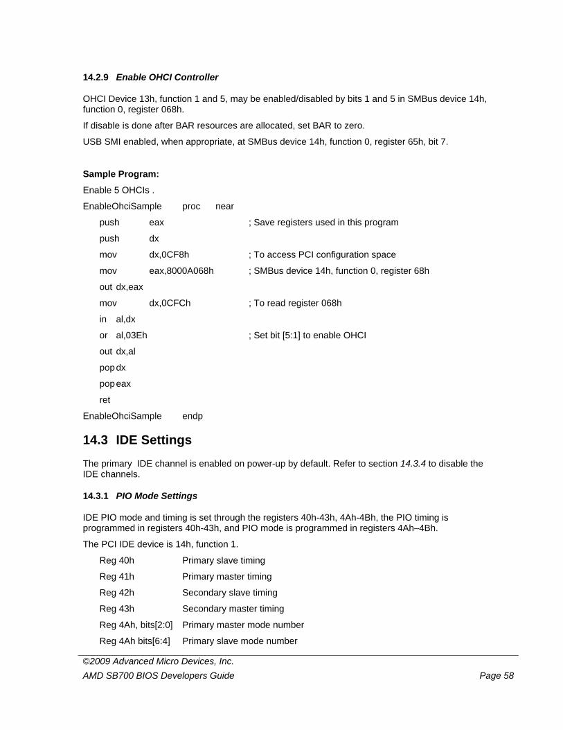
©2009 Advanced Micro Devices, Inc. AMD SB700 BIOS Developers Guide Page 58
14.2.9 Enable OHCI Controller
OHCI Device 13h, function 1 and 5, may be enabled/disabled by bits 1 and 5 in SMBus device 14h, function 0, register 068h.
If disable is done after BAR resources are allocated, set BAR to zero.
USB SMI enabled, when appropriate, at SMBus device 14h, function 0, register 65h, bit 7.
Sample Program:
Enable 5 OHCIs .
EnableOhciSample proc near
push eax ; Save registers used in this program
push dx
mov dx,0CF8h ; To access PCI configuration space
mov eax,8000A068h ; SMBus device 14h, function 0, register 68h
out dx,eax
mov dx,0CFCh ; To read register 068h
in al,dx
or al,03Eh ; Set bit [5:1] to enable OHCI
out dx,al
pop dx
pop eax
ret
EnableOhciSample endp
14.3 IDE Settings
The primary IDE channel is enabled on power-up by default. Refer to section 14.3.4 to disable the IDE channels.
14.3.1 PIO Mode Settings
IDE PIO mode and timing is set through the registers 40h-43h, 4Ah-4Bh, the PIO timing is programmed in registers 40h-43h, and PIO mode is programmed in registers 4Ah–4Bh.
The PCI IDE device is 14h, function 1.
Reg 40h Primary slave timing
Reg 41h Primary master timing
Reg 42h Secondary slave timing
Reg 43h Secondary master timing
Reg 4Ah, bits[2:0] Primary master mode number
Reg 4Ah bits[6:4] Primary slave mode number
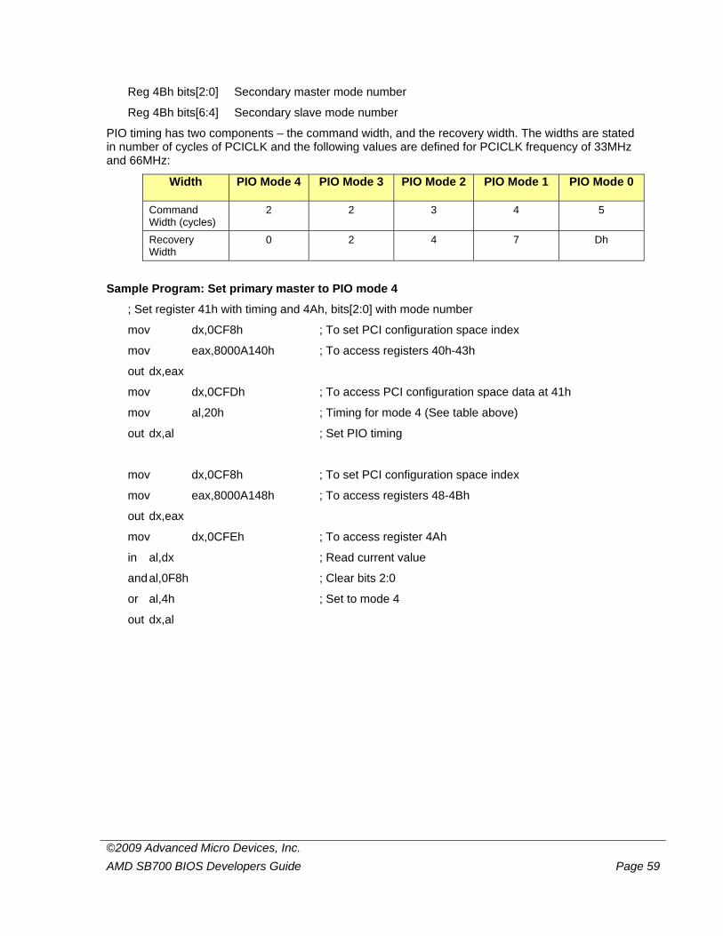
©2009 Advanced Micro Devices, Inc. AMD SB700 BIOS Developers Guide Page 59
Reg 4Bh bits[2:0] Secondary master mode number
Reg 4Bh bits[6:4] Secondary slave mode number
PIO timing has two components – the command width, and the recovery width. The widths are stated in number of cycles of PCICLK and the following values are defined for PCICLK frequency of 33MHz and 66MHz:
Width PIO Mode 4 PIO Mode 3 PIO Mode 2 PIO Mode 1 PIO Mode 0
Command Width (cycles)
2 2 3 4 5
Recovery Width
0 2 4 7 Dh
Sample Program: Set primary master to PIO mode 4
; Set register 41h with timing and 4Ah, bits[2:0] with mode number
mov dx,0CF8h ; To set PCI configuration space index
mov eax,8000A140h ; To access registers 40h-43h
out dx,eax
mov dx,0CFDh ; To access PCI configuration space data at 41h
mov al,20h ; Timing for mode 4 (See table above)
out dx,al ; Set PIO timing
mov dx,0CF8h ; To set PCI configuration space index
mov eax,8000A148h ; To access registers 48-4Bh
out dx,eax
mov dx,0CFEh ; To access register 4Ah
in al,dx ; Read current value
and al,0F8h ; Clear bits 2:0
or al,4h ; Set to mode 4
out dx,al
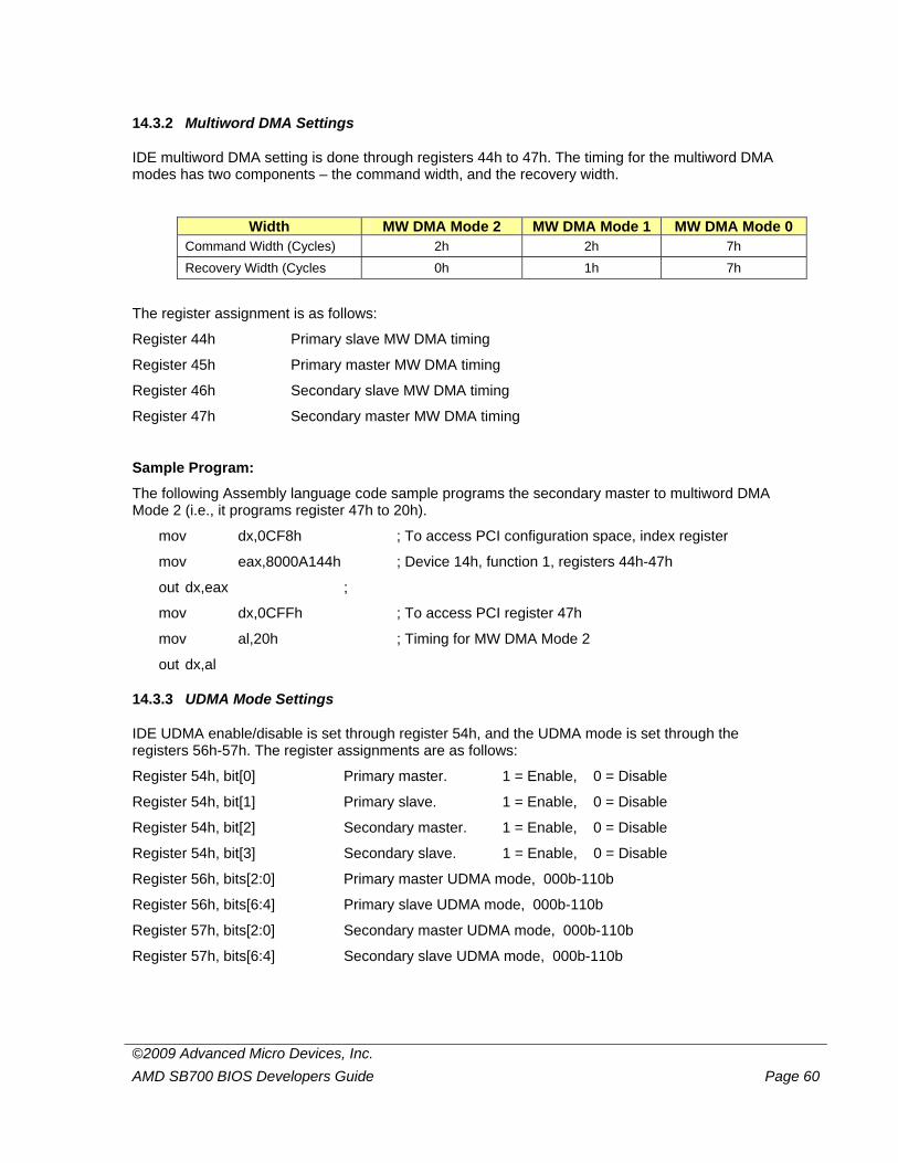
©2009 Advanced Micro Devices, Inc. AMD SB700 BIOS Developers Guide Page 60
14.3.2 Multiword DMA Settings
IDE multiword DMA setting is done through registers 44h to 47h. The timing for the multiword DMA modes has two components – the command width, and the recovery width.
Width MW DMA Mode 2 MW DMA Mode 1 MW DMA Mode 0 Command Width (Cycles) 2h 2h 7h Recovery Width (Cycles 0h 1h 7h
The register assignment is as follows:
Register 44h Primary slave MW DMA timing
Register 45h Primary master MW DMA timing
Register 46h Secondary slave MW DMA timing
Register 47h Secondary master MW DMA timing
Sample Program:
The following Assembly language code sample programs the secondary master to multiword DMA Mode 2 (i.e., it programs register 47h to 20h).
mov dx,0CF8h ; To access PCI configuration space, index register
mov eax,8000A144h ; Device 14h, function 1, registers 44h-47h
out dx,eax ;
mov dx,0CFFh ; To access PCI register 47h
mov al,20h ; Timing for MW DMA Mode 2
out dx,al
14.3.3 UDMA Mode Settings
IDE UDMA enable/disable is set through register 54h, and the UDMA mode is set through the registers 56h-57h. The register assignments are as follows:
Register 54h, bit[0] Primary master. 1 = Enable, 0 = Disable
Register 54h, bit[1] Primary slave. 1 = Enable, 0 = Disable
Register 54h, bit[2] Secondary master. 1 = Enable, 0 = Disable
Register 54h, bit[3] Secondary slave. 1 = Enable, 0 = Disable
Register 56h, bits[2:0] Primary master UDMA mode, 000b-110b
Register 56h, bits[6:4] Primary slave UDMA mode, 000b-110b
Register 57h, bits[2:0] Secondary master UDMA mode, 000b-110b
Register 57h, bits[6:4] Secondary slave UDMA mode, 000b-110b
©2009 Advanced Micro Devices, Inc. AMD SB700 BIOS Developers Guide Page 61
Sample Program
The sample program below sets the primary slave to UDMA mode 5:
push eax
push dx
; For primary slave, set register 56h, bits [6:4] to 5 for UDMA mode 5
mov dx,0CF8h ; To access PCI configuration space of IDE controller
mov eax,8000A154h ; Device 14h, function 1, register space 54h – 57h
out dx,eax
mov dx,0CFEh ; To access register 56h
in al,dx ; Current value of register 56h
and al,8Fh ; Clear bits 6:4.
or al,50h ; Set UDMA 5 mode for primary slave.
out dx,al
; Enable primary slave UDMA mode in register 54h, bit 1,
mov dx,CFCh ; To access register 54h
in al,dx ; Current value of register 54h
or al,02h ; Set bit 1
out dx,al
pop dx
pop eax
ret
14.3.4 IDE Channel Disable
To disable an IDE channel, the BIOS must:
1. Set IDE channel programmable logic enable bit in Reg09h.
2. Set IDE channel disable bit in Reg48h to disable IDE channel.
Note: No IDE I/O port access is allowed between step (1) and step (2). It is recommended that the BIOS execute step (2) immediately after step (1). There should be no ‘in’ instruction between two ‘out’ instructions to register 09h and 48h.
After the IDE disable sequence, the IDE channel programmable logic enable bit will be cleared automatically.
Sample program: Disable secondary channel
; Read current register 48h-49h on IDE controller
push eax push bx push dx mov eax,8000A148h ; To modify register 48h on the IDE controller
©2009 Advanced Micro Devices, Inc. AMD SB700 BIOS Developers Guide Page 62
mov dx,0CF8h ; PCI index register out dx,eax ; Set index for register 48h-4Bh mov dx,0CFCh ; Set PCI data register for 48h in ax,dx ; Read register 49h
mov bx,ax ; Save current 48h-49h registers ; Unlock the IDE controller to be enabled/disabled bit mov eax,8000A108h ; To write to PCI register 08h on IDE controller mov dx,0CF8h ; PCI index register out dx,eax ; Set index for registers 08h – 0Bh mov dx,0CFDh ; To read register 09h in al,dx ; Read register 09h or al,08h ; Set bit 3 to enable secondary channel program out dx,al ; Write back to register ; Disable the secondary IDE channel. The register 48h-49h is saved in BX mov eax,8000A148h ; To modify register 48h on the IDE controller mov dx,0CF8h ; PCI index register out dx,eax ; Set index for register 48h-4Bh mov dx,0CFCh ; Set PCI data register for 49h or bx,0100h ; Set bit 8 of 48h mov ax,bx out dx,ax
; Lock in the secondary channel to enable/disable bit mov eax,8000A108h ; To write to PCI register 08h on IDE controller mov dx,0CF8h ; PCI index register out dx,eax ; Set index for registers 08h – 0Bh mov dx,0CFDh ; To read register 09h in al,dx ; Read register 09h and al,0F7h ; Clear bit 3 to enable secondary channel program out dx,al ; Write back to register pop dx pop bx pop eax
; End of secondary channel disable
©2009 Advanced Micro Devices, Inc. AMD SB700 BIOS Developers Guide Page 63
14.3.5 IDE Channel Enable
The primary IDE channel is enabled as power-on default. To enable an IDE channel after they have been disabled, the BIOS must:
1. Set the IDE channel programmable logic enable bit in Reg09h.
2. Clear the IDE channel disable bit in Reg48h to enable the IDE channel.
Note: No IDE I/O port access is allowed between step (1) and step (2). It is recommended that the BIOS execute step (2) immediately after step (1). There should be no ‘in’ instruction between two ‘out’ instructions to register 09h and 48h.
Sample Program: Enable Primary IDE channel
; Read current register 48h-49h on IDE controller
push eax push bx push dx mov eax,8000A148h ; To modify register 48h on the IDE controller mov dx,0CF8h ; PCI index register out dx,eax ; Set index for register 48h-4Bh mov dx,0CFCh ; Set PCI data register for 48h in ax,dx ; Read register 49h
mov bx,ax ; Save current 48h-49h registers ; Unlock the IDE controller to enable/disable bit mov eax,8000A108h ; To write to PCI register 08h on IDE controller mov dx,0CF8h ; PCI index register out dx,eax ; Set index for registers 08h – 0Bh mov dx,0CFDh ; To read register 09h in al,dx ; Read register 09h or al,02h ; Set bit 1 to enable primary channel program out dx,al ; Write back to register ; Enable the primary IDE channel. The register 48h-49h is saved in BX mov eax,8000A148h ; To modify register 48h on the IDE controller mov dx,0CF8h ; PCI index register out dx,eax ; Set index for register 48h-4Bh mov dx,0CFCh ; Set PCI data register for 49h and bx,0FFFEh ; Clear bit 0 of 48h mov ax,bx out dx,ax
; Lock in the primary channel to enable/disable bit mov eax,8000A108h ; To write to PCI register 08h on IDE controller mov dx,0CF8h ; PCI index register out dx,eax ; Set index for registers 08h – 0Bh mov dx,0CFDh ; To read register 09h
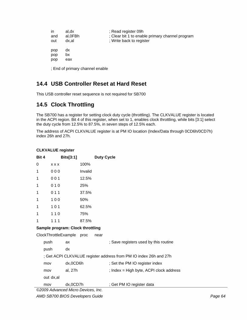
©2009 Advanced Micro Devices, Inc. AMD SB700 BIOS Developers Guide Page 64
in al,dx ; Read register 09h and al,0FBh ; Clear bit 1 to enable primary channel program out dx,al ; Write back to register pop dx pop bx pop eax ; End of primary channel enable
14.4 USB Controller Reset at Hard Reset
This USB controller reset sequence is not required for SB700
14.5 Clock Throttling
The SB700 has a register for setting clock duty cycle (throttling). The CLKVALUE register is located in the ACPI region. Bit 4 of this register, when set to 1, enables clock throttling, while bits [3:1] select the duty cycle from 12.5% to 87.5%, in seven steps of 12.5% each.
The address of ACPI CLKVALUE register is at PM IO location (Index/Data through 0CD6h/0CD7h) index 26h and 27h.
CLKVALUE register
Bit 4 Bits[3:1] Duty Cycle
0 x x x 100%
1 0 0 0 Invalid
1 0 0 1 12.5%
1 0 1 0 25%
1 0 1 1 37.5%
1 1 0 0 50%
1 1 0 1 62.5%
1 1 1 0 75%
1 1 1 1 87.5%
Sample program: Clock throttling
ClockThrottleExample proc near
push ax ; Save registers used by this routine
push dx
; Get ACPI CLKVALUE register address from PM IO index 26h and 27h
mov dx,0CD6h ; Set the PM IO register index
mov al, 27h ; Index = High byte, ACPI clock address
out dx,al
mov dx,0CD7h ; Get PM IO register data
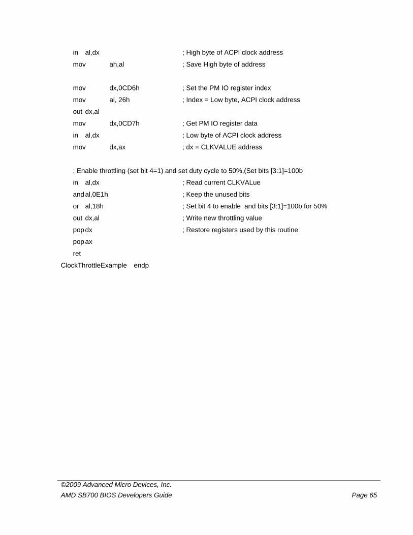
©2009 Advanced Micro Devices, Inc. AMD SB700 BIOS Developers Guide Page 65
in al,dx ; High byte of ACPI clock address
mov ah,al ; Save High byte of address
mov dx,0CD6h ; Set the PM IO register index
mov al, 26h ; Index = Low byte, ACPI clock address
out dx,al
mov dx,0CD7h ; Get PM IO register data
in al,dx ; Low byte of ACPI clock address
mov dx,ax ; dx = CLKVALUE address
; Enable throttling (set bit 4=1) and set duty cycle to 50%,(Set bits [3:1]=100b
in al,dx ; Read current CLKVALue
and al,0E1h ; Keep the unused bits
or al,18h ; Set bit 4 to enable and bits [3:1]=100b for 50%
out dx,al ; Write new throttling value
pop dx ; Restore registers used by this routine
pop ax
ret
ClockThrottleExample endp
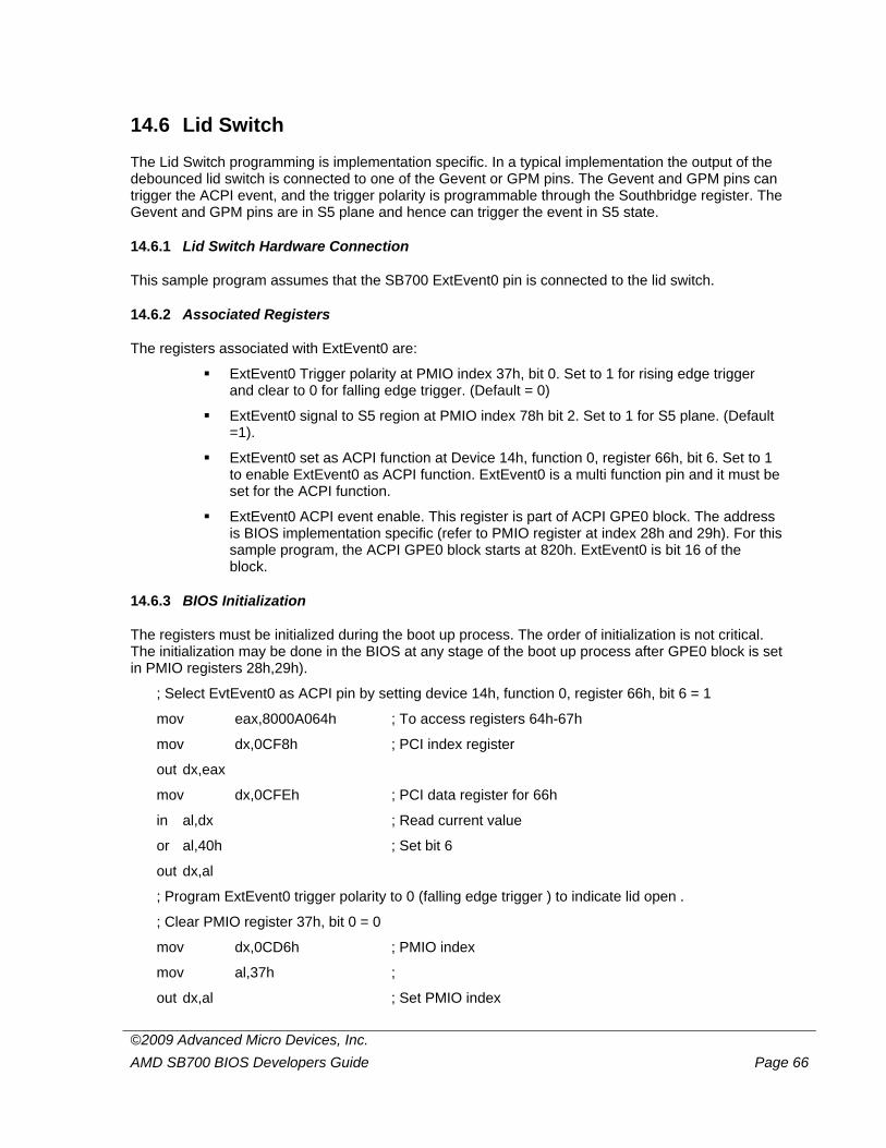
©2009 Advanced Micro Devices, Inc. AMD SB700 BIOS Developers Guide Page 66
14.6 Lid Switch
The Lid Switch programming is implementation specific. In a typical implementation the output of the debounced lid switch is connected to one of the Gevent or GPM pins. The Gevent and GPM pins can trigger the ACPI event, and the trigger polarity is programmable through the Southbridge register. The Gevent and GPM pins are in S5 plane and hence can trigger the event in S5 state.
14.6.1 Lid Switch Hardware Connection
This sample program assumes that the SB700 ExtEvent0 pin is connected to the lid switch.
14.6.2 Associated Registers
The registers associated with ExtEvent0 are:
ExtEvent0 Trigger polarity at PMIO index 37h, bit 0. Set to 1 for rising edge trigger and clear to 0 for falling edge trigger. (Default = 0)
ExtEvent0 signal to S5 region at PMIO index 78h bit 2. Set to 1 for S5 plane. (Default =1).
ExtEvent0 set as ACPI function at Device 14h, function 0, register 66h, bit 6. Set to 1 to enable ExtEvent0 as ACPI function. ExtEvent0 is a multi function pin and it must be set for the ACPI function.
ExtEvent0 ACPI event enable. This register is part of ACPI GPE0 block. The address is BIOS implementation specific (refer to PMIO register at index 28h and 29h). For this sample program, the ACPI GPE0 block starts at 820h. ExtEvent0 is bit 16 of the block.
14.6.3 BIOS Initialization
The registers must be initialized during the boot up process. The order of initialization is not critical. The initialization may be done in the BIOS at any stage of the boot up process after GPE0 block is set in PMIO registers 28h,29h).
; Select EvtEvent0 as ACPI pin by setting device 14h, function 0, register 66h, bit 6 = 1
mov eax,8000A064h ; To access registers 64h-67h
mov dx,0CF8h ; PCI index register
out dx,eax
mov dx,0CFEh ; PCI data register for 66h
in al,dx ; Read current value
or al,40h ; Set bit 6
out dx,al
; Program ExtEvent0 trigger polarity to 0 (falling edge trigger ) to indicate lid open .
; Clear PMIO register 37h, bit 0 = 0
mov dx,0CD6h ; PMIO index
mov al,37h ;
out dx,al ; Set PMIO index
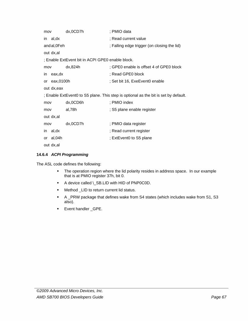
©2009 Advanced Micro Devices, Inc. AMD SB700 BIOS Developers Guide Page 67
mov dx,0CD7h ; PMIO data
in al,dx ; Read current value
and al,0Feh ; Falling edge trigger (on closing the lid)
out dx,al
; Enable ExtEvent bit in ACPI GPE0 enable block.
mov dx,824h ; GPE0 enable is offset 4 of GPE0 block
in eax,dx ; Read GPE0 block
or eax,0100h ; Set bit 16, ExeEvent0 enable
out dx,eax
; Enable ExtEvent0 to S5 plane. This step is optional as the bit is set by default.
mov dx,0CD6h ; PMIO index
mov al,78h ; S5 plane enable register
out dx,al
mov dx,0CD7h ; PMIO data register
in al,dx ; Read current register
or al,04h ; ExtEvent0 to S5 plane
out dx,al
14.6.4 ACPI Programming
The ASL code defines the following:
The operation region where the lid polarity resides in address space. In our example that is at PMIO register 37h, bit 0.
A device called \_SB.LID with HID of PNP0C0D.
Method _LID to return current lid status.
A _PRW package that defines wake from S4 states (which includes wake from S1, S3 also).
Event handler _GPE.
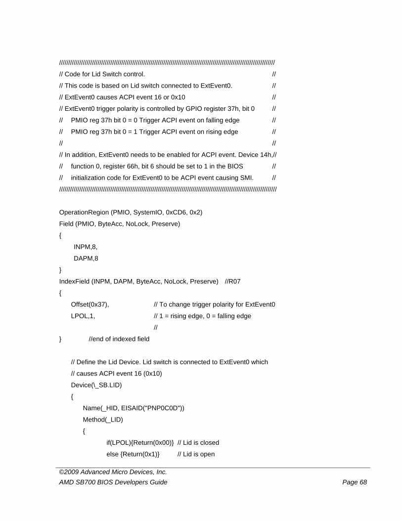
©2009 Advanced Micro Devices, Inc. AMD SB700 BIOS Developers Guide Page 68
//////////////////////////////////////////////////////////////////////////////////////////////////////////////////////
// Code for Lid Switch control. //
// This code is based on Lid switch connected to ExtEvent0. //
// ExtEvent0 causes ACPI event 16 or 0x10 //
// ExtEvent0 trigger polarity is controlled by GPIO register 37h, bit 0 //
// PMIO reg 37h bit 0 = 0 Trigger ACPI event on falling edge //
// PMIO reg 37h bit 0 = 1 Trigger ACPI event on rising edge //
// //
// In addition, ExtEvent0 needs to be enabled for ACPI event. Device 14h,//
// function 0, register 66h, bit 6 should be set to 1 in the BIOS //
// initialization code for ExtEvent0 to be ACPI event causing SMI. //
///////////////////////////////////////////////////////////////////////////////////////////////////////////////////////
OperationRegion (PMIO, SystemIO, 0xCD6, 0x2)
Field (PMIO, ByteAcc, NoLock, Preserve)
{
INPM,8,
DAPM,8
}
IndexField (INPM, DAPM, ByteAcc, NoLock, Preserve) //R07
{
Offset(0x37), // To change trigger polarity for ExtEvent0
LPOL,1, // 1 = rising edge, 0 = falling edge
//
} //end of indexed field
// Define the Lid Device. Lid switch is connected to ExtEvent0 which
// causes ACPI event 16 (0x10)
Device(\_SB.LID)
{
Name(_HID, EISAID("PNP0C0D"))
Method(_LID)
{
if(LPOL){Return(0x00)} // Lid is closed
else {Return(0x1)} // Lid is open
©2009 Advanced Micro Devices, Inc. AMD SB700 BIOS Developers Guide Page 69
}
Name(_PRW, Package(2)
{ 0x10, 0x03} // ACPI event 0x10 can wake-up from S3
)
}
//ACPI event
Scope(\_GPE)
{ Method(_L10)
{
Not(LPOL, LPOL) // Reverse the polarity from sleep to wake and vice versa
Notify(\_SB.LID, 0x80) // Notify the OS that status has changed.
}
}
14.7 SATA Hot Plug Sample Program
Scope(\_GPE)
{
Method(_L1F,0x0,Notserialized) // GPE0 Block bit 31 is used for SATA hot plug
{
sleep(2000)
// For SATA at Bus 0, Device 12h, Function 0, channel 0 device
// Check if change in the status of the Serial ATA PHY
if(\_SB_.PCI0.SATA.STA0) { // BAR5, offset 10ah, bit0
Notify(\_SB.PCI0.SATA.PRID.P_D0, 0x00)
sleep(2000)
Notify(\_SB.PCI0.SATA.PRID, 0x01)
sleep(2000)
store(\_SB_.PCI0.SATA.STA0,\_SB_.PCI0.SATA.STA0) // Clear Status of master SATA
}
// For SATA at Bus 0, Device 12h, Function 0, channel 1 device
// Check if change in the status of the Serial ATA PHY
if(\_SB_.PCI0.SATA.STA1) { // BAR5, offset 18Ah, bit 0
Notify(\_SB.PCI0.SATA.SECD.S_D0, 0x00)
sleep(2000)
Notify(\_SB.PCI0.SATA.SECD, 0x01)
©2009 Advanced Micro Devices, Inc. AMD SB700 BIOS Developers Guide Page 70
sleep(2000)
store(\_SB_.PCI0.SATA.STA1,\_SB_.PCI0.SATA.STA1) // Clear Status of slave SATA
}
// For SATA at Bus 0, Device 11h, Function 0 , channel 0 device
// Check if change in the status of the Serial ATA PHY
if(\_SB_.PCI0.SAT2.STA0){ // BAR5, offset 10ah, bit0
Notify(\_SB.PCI0.SAT2.PRID.P_D0, 0x00)
sleep(2000)
Notify(\_SB.PCI0.SAT2.PRID, 0x01)
sleep(2000)
store(\_SB_.PCI0.SAT2.STA0,\_SB_.PCI0.SAT2.STA0) // Clear Status of master SATA
}
// For SATA at Bus 0, Device 11h, Function 0, channel 1 device
// Check if change in the status of the Serial ATA PHY
if(\_SB_.PCI0.SAT2.STA1) { //BAR4, offset 18Ah, bit 0
Notify(\_SB.PCI0.SAT2.SECD.S_D0, 0x00)
sleep(2000)
Notify(\_SB.PCI0.SAT2.SECD, 0x01)
sleep(2000)
store(\_SB_.PCI0.SAT2.STA1,\_SB_.PCI0.SAT2.STA1) // Clear Status of slave SATA
}
} // End of Method(_L1F)
} // End of Scope(\_GPE)
Scope(\_SB_.PCI0.SATA) // Bus 0, Device 12h, Function 0
{
OperationRegion(BAR5, SystemMemory, 0xFFF80000, 0x1000) // The address should // be replaced by the // BIOS
Field(BAR5, AnyAcc, NoLock, Preserve)
{
Offset(0x104), // Channel 0
CSTX, 1, // Device detected but no communication with Phy
CST0, 1, // Communication with Phy established. (Physgood)
©2009 Advanced Micro Devices, Inc. AMD SB700 BIOS Developers Guide Page 71
Offset(0x10A), // Channel 0
STA0, 1, // Change in Phy status
Offset(0x184), // Channel 1
CSTY, 1, // Device detected but no communications with Phy
CST1, 1, // Communication with Phy established (Physgood)
Offset(0x18A), // Channel 1
STA1, 1, // Changes in Phy status
} // End of Field(BAR5….)
Method(_INI) { // For Bus 0, Device 12h, Function 0
if(\_SB_.PCI0.SATA.STA0){
store(\_SB_.PCI0.SATA.STA0,\_SB_.PCI0.SATA.STA0) // Clear channel 0 SATA status
}
if(\_SB_.PCI0.SATA.STA1){
store(\_SB_.PCI0.SATA.STA1,\_SB_.PCI0.SATA.STA1) // Clear channel 1 SATA status
}
} // End of Method (_INI)
Device(PRID) {
Name(_ADR, 0) // IDE Primary Channel
Device(P_D0) {
Name(_ADR, 0) // Drive 0 - Master
Method(_STA,0){
if (\_SB_.PCI0.SATA.CST0) { // If SATA detected
return(0x0f)
} else {
return (0x00) }
} End of Method (_STA )
} // End of P_D0
} // End of PRID
©2009 Advanced Micro Devices, Inc. AMD SB700 BIOS Developers Guide Page 72
Device(SECD) {
Name(_ADR, 1) // IDE Secondary Channel
Device(S_D0) {
Name(_ADR, 0) // Drive 0 - Master
Method(_STA,0){
if (\_SB_.PCI0.SATA.CST1) { // If SATA detected
return (0x0f)
}
else {
return (0x00) } /
} // End of Method (_STA)
} // End of S_D0
} // End of SECD
} // End of Scope(_SB.PCI0.SATA)
// Bus 0, Device 11h, Function 0
Scope(\_SB_.PCI0.SAT2)
{
OperationRegion(BAR5, SystemMemory, 0xFFF80000, 0x1000) // Replace address in BIOS
Field(BAR5, AnyAcc, NoLock, Preserve)
{
Offset(0x104), //Channel 0
CSTX, 1, // Device detected but no communication with Phy
CST0, 1, // Communication with PHY established
Offset(0x10A), // Channel 0
STA0, 1, // Change in PHY status
Offset(0x184), // Channel 1
CSTY, 1, // Device detected but no communication with PHY
CST1, 1, // Communication with PHY established
Offset(0x18A), //Channel 1
STA1, 1, // Change in PHY status
©2009 Advanced Micro Devices, Inc. AMD SB700 BIOS Developers Guide Page 73
} // End of Field
Method(_INI) { // For Bus 0, Device 11h, Function 0
if(\_SB_.PCI0.SAT2.STA0){
store(\_SB_.PCI0.SAT2.STA0,\_SB_.PCI0.SAT2.STA0) // Clear SATA channel0 status
}
if(\_SB_.PCI0.SAT2.STA1)
{
store(\_SB_.PCI0.SAT2.STA1,\_SB_.PCI0.SAT2.STA1) // Clear SATA channel 1 status
}
} // End of Method(_INI)
Device(PRID) {
Name(_ADR, 0) // IDE Primary Channel
Device(P_D0) {
Name(_ADR, 0) // Drive 0 - Master
Method(_STA,0){
if (\_SB_.PCI0.SAT2.CST0) { // If SATA detected
return(0x0f)
}
else {
return (0x00)
}
} // End of Method(_STA)
} // End of P_D0
} // End of PRID
Device(SECD) {
Name(_ADR, 1) // IDE Secondary Channel
Device(S_D0) {
Name(_ADR, 0) // Drive 0 - Master
©2009 Advanced Micro Devices, Inc. AMD SB700 BIOS Developers Guide Page 74
Method(_STA,0){
if (\_SB_.PCI0.SAT2.CST1) { // If SATA detected
return(0x0f)
}
else {
return (0x00)
}
} //End of Method(_STA)
} // End of S_D0
} // End of SECD
} // End of Scope(\_SB_.PCI0.SAT2)
14.8 Temperature Limit Shutdown through SMI#
The program to shut down the system when the temperature exceeds a pre-set limit requires the following:
1. A temperature sensing diode or thermistor positioned under the CPU socket. 2. A Super I/O device capable of monitoring the temperature and toggle an SMI# line when
the temperature exceeds the pre-set limit. 3. SMI programming in the SB700 to shut down the system.
The discussion below assumes that an ITE-8712 Super I/O is present in the system and is connected to the thermal diode to measure temperature-1 and temperature-2, and a thermistor to measure temperature-3. This code example shows thermal programming in the Super I/O, and SMI programming related to thermal shutdown.
Please refer to ITE-8712 Super I/O device manual for register details.
This code example assumes that the GP47 from Super I/O is connected to the ExtEvent1 pin on the SB700.
©2009 Advanced Micro Devices, Inc. AMD SB700 BIOS Developers Guide Page 75
14.8.1 Setting Up ITE 8712 Super I/O Registers
ITE 8712 Super I/O registers are set during the boot up process through the BIOS program.
1. Set the Environmental Controller base address.
Select a base address in the I/O range which is not used by any device and is also accessible to the LPC. The address range is 8 bytes. In this example the I/O address 228h – 22Fh will be used. This address is set in Super I/O logical device 04h, registers 60h, and 61h. After the base address is set, the environment registers are accessed by index/data method at base address+5 as index, and base address+6 as data. For this example the index/data address would be 22Dh/22Eh. ; Define equates for index/data, shutdown temperature, and Super I/O access port.
Sensor_Port EQU 22Dh TemperatureLimit EQU 75
SuperIo_Config_Port EQU 2EH
call SuperIoEnterConfig ; Write 87h, 01h, 55h, 55h to SuperIo ; Enable the access to device 04 registers, i.e. set Super I/O address ; register to 04
; Device 04 is the Environment controller mov dx,2Eh ; Super I/O index mov al, 07h ; Register 07 is device select out dx,al mov dx,2Fh ; Super I/O data mov al, 04h ; Set register to 04 out dx,al ; Logical Device Number (LDN) is now set to 04. ; Set Base address to 0228h in registers 60h and 61h of this LDN = 04 ; Set MS byte of base address to 02h mov dx,2Eh mov dx,60h out dx,al mov dx,2Fh ; Super I/O index mov al,02h ; MS byte of 0228h out dx,al ; Set LS byte of the base address to 28h mov dx,2Eh mov dx,61h out dx,al
©2009 Advanced Micro Devices, Inc. AMD SB700 BIOS Developers Guide Page 76
mov dx,2Fh ; Super I/O index mov al,28h ; MS byte of 0228h out dx,al
; The environment (temperature, voltage etc.) registers can now be accessed ; through Base address + 5 (index), and base address + 6, i.e. 22Dh and 22Eh
mov ah, TemperatureLimit ; Selected through setup or OEM ; Set limit for 1st Thermistor ; Register 40h is for upper limit, register 41h is for lower limit ; If lower limit is set to 7Fh, then the temperature controller is in the ; comparator mode mov dx,Sensor_Port ; The register is written through index at ; 22Dh mov al,40h ; To set the upper limit out dx,al mov dx,Sensor_Port+1 ; The temperature value is written through ; 22Eh mov al,ah ; Get the Temperature upper limit out dx,al mov dx,Sensor_Port ; The register is written through index at ; 22Dh mov al,41h ; To set the lower limit out dx,al mov dx,Sensor_Port+1 mov al,7fh ; Lower limit of 7Fh to enable the comparator mode out dx,al ; Set limit for 2nd Thermistor ; Register 42h is for upper limit, register 43h is for lower limit ; If lower limit is 7Fh then it is comparator mode mov dx,Sensor_Port ; The register is written through index at ; 22Dh mov al,42h ; To set the upper limit out dx,al mov dx,Sensor_Port+1 ; The temperature value is written through ; 22Eh mov al,ah ; Get the Temperature upper limit out dx,al mov dx,Sensor_Port ; The register is written through index at ; 22Dh mov al,43h ; To set the lower limit out dx,al

©2009 Advanced Micro Devices, Inc. AMD SB700 BIOS Developers Guide Page 77
mov dx,Sensor_Port+1 ; The temperature value is written through ; 22Eh mov al,7fh ; For comparator mode out dx,al ; Set limit for 3rd Thermistor ; Register 44h is for upper limit, register 45h is for lower limit ; If lower limit is 7Fh then it is comparator mode mov dx,Sensor_Port ; The register is written through index at ; 22Dh mov al,44h ; To set the upper limit out dx,al mov dx,Sensor_Port+1 ; The temperature value is written through ; 22Eh mov al,ah ; Get the temperature upper limit out dx,al mov dx,Sensor_Port ; The register is written through index at ; 22Dh mov al,45h ; To set the lower limit out dx,al mov dx,Sensor_Port+1 ; The temperature value is written through ; 22Eh mov al,7Fh ; For comparator mode out dx,al ; Set Thermal out limit registers at 52h, 53h, 54h mov dx,Sensor_Port ; The register is written through index at ; 22Dh mov al,52h ; Thermal limit for diode 1 out dx,al mov dx,Sensor_Port+1 ; The temperature value is written through ; 22Eh mov al,ah ; Get temperature upper limit out dx,al mov dx,Sensor_Port ; The register is written through index at ; 22Dh mov al,53h ; Thermal limit for diode 2 out dx,al mov dx,Sensor_Port+1 ; The temperature value is written through ; 22Eh mov al,ah ; Get temperature upper limit out dx,al mov dx,Sensor_Port ; The register is written through index at ; 22Dh mov al,54h ; Thermal limit for thermistor 3 out dx,al

©2009 Advanced Micro Devices, Inc. AMD SB700 BIOS Developers Guide Page 78
mov dx,Sensor_Port+1 ; The temperature value is written through ; 22Eh mov al,ah ; Get temperature upper limit out dx,al ; Read status from register 03 to clear the status mov dx,Sensor_Port ; The register is read through index at 22Dh mov al,03h out dx,al mov dx,Sensor_Port+1 ; The register is read through data at 22Eh in al,dx ; Enable Interrupt/SMI# register at 00. mov dx,Sensor_Port ; The register is written through index at ; 22Dh mov al,00h out dx,al mov dx,Sensor_Port+1 ; The register is written through data at ; 22Eh in al,dx or al,07h ; Enable IRQ, SMI# and enable monitoring out dx,al ; In logical device 7, set SMI registers, thermal out register, and enable the ; SMI. ; 1. Set logical device to 7 mov al,07h mov dx,SuperIo_Config_Port out dx,al mov al,07h inc dx out dx,al ; 2. Set SMI pin to GP47 ( 00 100 111 = 27h) in reg 0f4h ; Register F4 is SMI mapping register mov al,0f4h mov dx,SuperIo_Config_Port out dx,al inc dx mov al,27h out dx,al
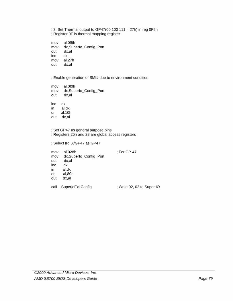
©2009 Advanced Micro Devices, Inc. AMD SB700 BIOS Developers Guide Page 79
; 3. Set Thermal output to GP47(00 100 111 = 27h) in reg 0F5h ; Register 0F is thermal mapping register mov al,0f5h mov dx,SuperIo_Config_Port out dx,al inc dx mov al,27h out dx,al ; Enable generation of SMI# due to environment condition mov al,0f0h mov dx,SuperIo_Config_Port out dx,al inc dx in al,dx or al,10h out dx,al ; Set GP47 as general purpose pins ; Registers 25h and 28 are global access registers ; Select IRTX/GP47 as GP47 mov al,028h ; For GP-47 mov dx,SuperIo_Config_Port out dx,al inc dx in al,dx or al,80h out dx,al call SuperioExitConfig ; Write 02, 02 to Super IO
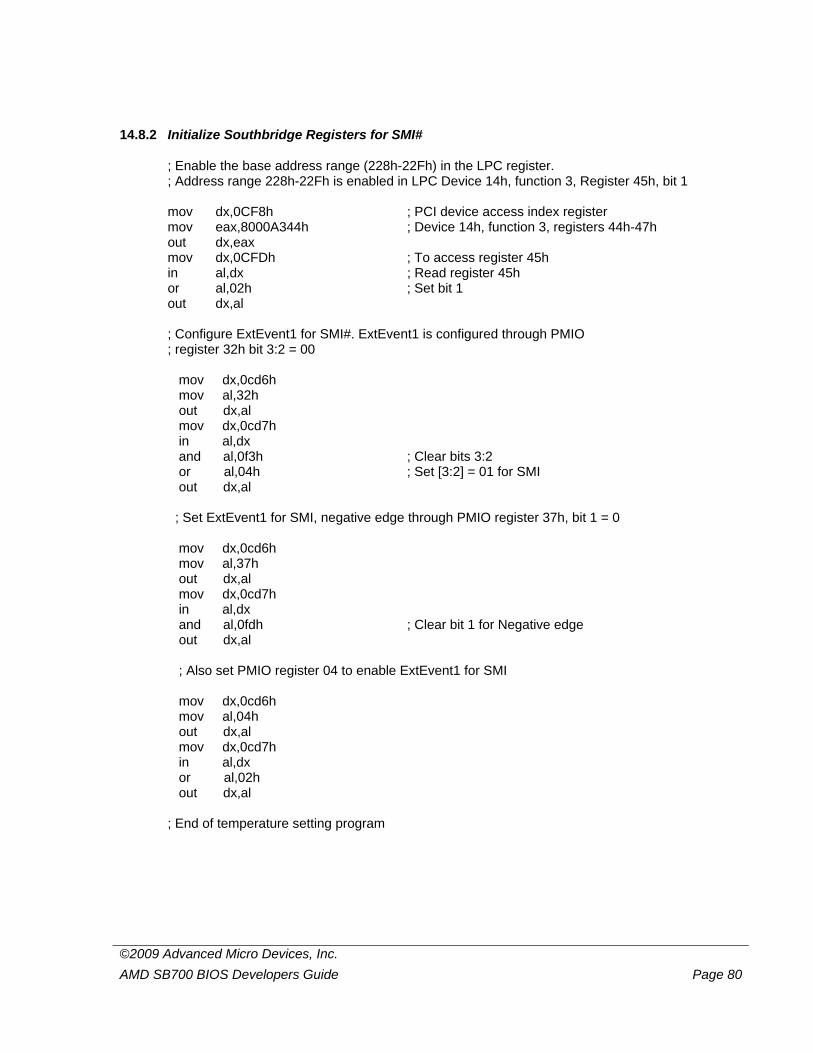
©2009 Advanced Micro Devices, Inc. AMD SB700 BIOS Developers Guide Page 80
14.8.2 Initialize Southbridge Registers for SMI#
; Enable the base address range (228h-22Fh) in the LPC register. ; Address range 228h-22Fh is enabled in LPC Device 14h, function 3, Register 45h, bit 1
mov dx,0CF8h ; PCI device access index register mov eax,8000A344h ; Device 14h, function 3, registers 44h-47h out dx,eax mov dx,0CFDh ; To access register 45h in al,dx ; Read register 45h or al,02h ; Set bit 1 out dx,al ; Configure ExtEvent1 for SMI#. ExtEvent1 is configured through PMIO ; register 32h bit 3:2 = 00 mov dx,0cd6h mov al,32h out dx,al mov dx,0cd7h in al,dx and al,0f3h ; Clear bits 3:2 or al,04h ; Set [3:2] = 01 for SMI out dx,al ; Set ExtEvent1 for SMI, negative edge through PMIO register 37h, bit 1 = 0 mov dx,0cd6h mov al,37h out dx,al mov dx,0cd7h in al,dx and al,0fdh ; Clear bit 1 for Negative edge out dx,al ; Also set PMIO register 04 to enable ExtEvent1 for SMI mov dx,0cd6h mov al,04h out dx,al mov dx,0cd7h in al,dx or al,02h out dx,al ; End of temperature setting program
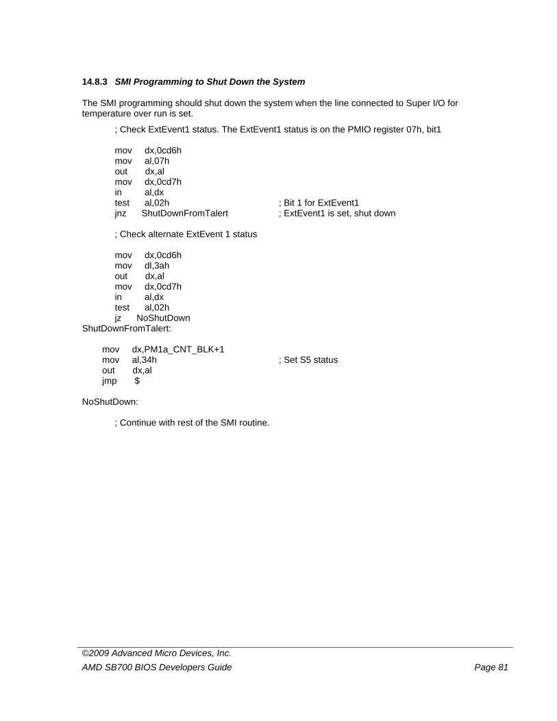
©2009 Advanced Micro Devices, Inc. AMD SB700 BIOS Developers Guide Page 81
14.8.3 SMI Programming to Shut Down the System
The SMI programming should shut down the system when the line connected to Super I/O for temperature over run is set.
; Check ExtEvent1 status. The ExtEvent1 status is on the PMIO register 07h, bit1
mov dx,0cd6h mov al,07h out dx,al mov dx,0cd7h in al,dx test al,02h ; Bit 1 for ExtEvent1 jnz ShutDownFromTalert ; ExtEvent1 is set, shut down
; Check alternate ExtEvent 1 status
mov dx,0cd6h mov dl,3ah out dx,al mov dx,0cd7h in al,dx test al,02h jz NoShutDown
ShutDownFromTalert: mov dx,PM1a_CNT_BLK+1 mov al,34h ; Set S5 status out dx,al jmp $ NoShutDown: ; Continue with rest of the SMI routine.
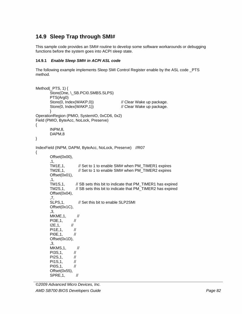
©2009 Advanced Micro Devices, Inc. AMD SB700 BIOS Developers Guide Page 82
14.9 Sleep Trap through SMI#
This sample code provides an SMI# routine to develop some software workarounds or debugging functions before the system goes into ACPI sleep state.
14.9.1 Enable Sleep SMI# in ACPI ASL code
The following example implements Sleep SMI Control Register enable by the ASL code _PTS method.
Method(_PTS, 1) { Store(One, \_SB.PCI0.SMBS.SLPS) PTS(Arg0) Store(0, Index(WAKP,0)) // Clear Wake up package. Store(0, Index(WAKP,1)) // Clear Wake up package. }
OperationRegion (PMIO, SystemIO, 0xCD6, 0x2) Field (PMIO, ByteAcc, NoLock, Preserve) {
INPM,8, DAPM,8
} IndexField (INPM, DAPM, ByteAcc, NoLock, Preserve) //R07 {
Offset(0x00), ,1, TM1E,1, // Set to 1 to enable SMI# when PM_TIMER1 expires TM2E,1, // Set to 1 to enable SMI# when PM_TIMER2 expires Offset(0x01), ,1, TM1S,1, // SB sets this bit to indicate that PM_TIMER1 has expired TM2S,1, // SB sets this bit to indicate that PM_TIMER2 has expired Offset(0x04), ,7, SLPS,1, // Set this bit to enable SLP2SMI Offset(0x1C), ,3, MKME,1, // PI3E,1, // I2E,1, // PI1E,1, // PI0E,1, // Offset(0x1D), ,3, MKMS,1, // PI3S,1, // PI2S,1, // PI1S,1, // PI0S,1, // Offset(0x55), SPRE,1, //
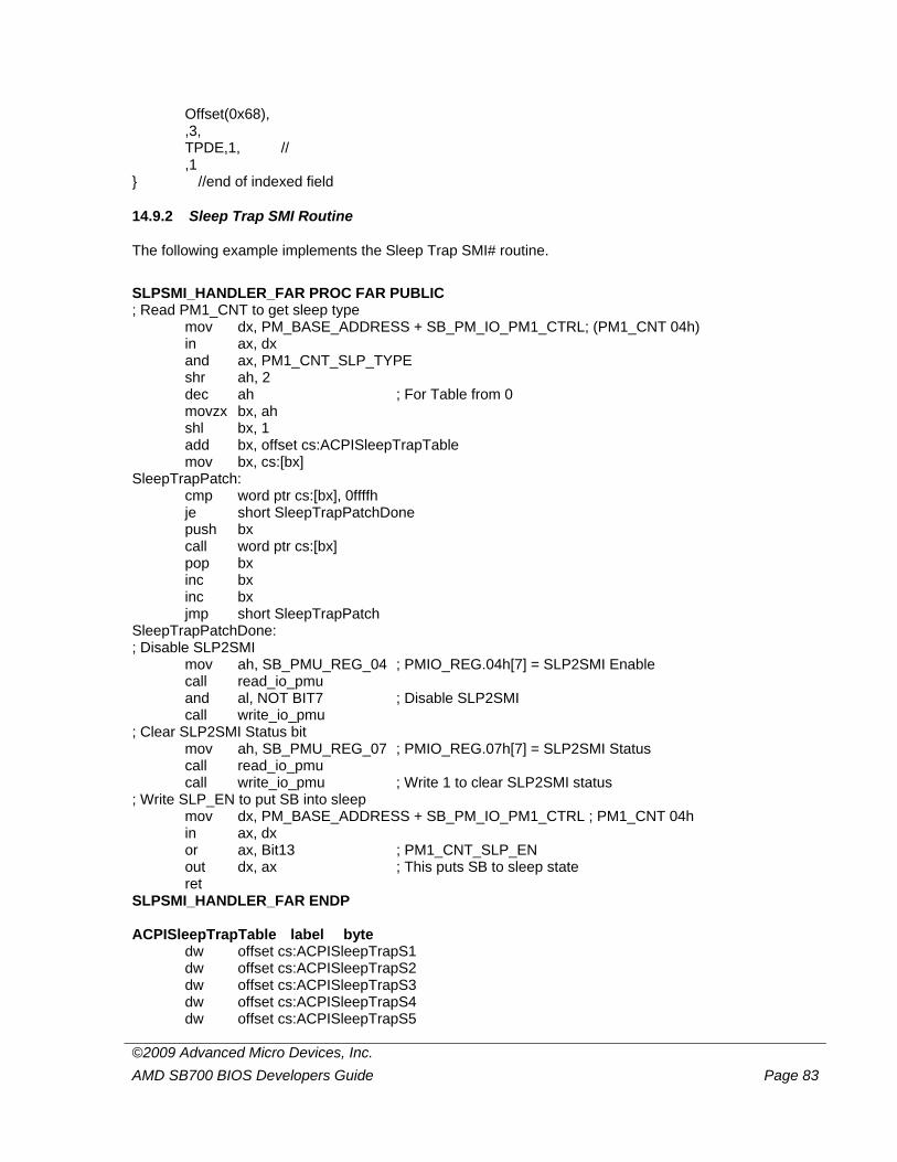
©2009 Advanced Micro Devices, Inc. AMD SB700 BIOS Developers Guide Page 83
Offset(0x68), ,3, TPDE,1, // ,1
} //end of indexed field
14.9.2 Sleep Trap SMI Routine
The following example implements the Sleep Trap SMI# routine.
SLPSMI_HANDLER_FAR PROC FAR PUBLIC ; Read PM1_CNT to get sleep type
mov dx, PM_BASE_ADDRESS + SB_PM_IO_PM1_CTRL; (PM1_CNT 04h) in ax, dx and ax, PM1_CNT_SLP_TYPE shr ah, 2 dec ah ; For Table from 0 movzx bx, ah shl bx, 1 add bx, offset cs:ACPISleepTrapTable mov bx, cs:[bx]
SleepTrapPatch: cmp word ptr cs:[bx], 0ffffh je short SleepTrapPatchDone push bx call word ptr cs:[bx] pop bx inc bx inc bx jmp short SleepTrapPatch
SleepTrapPatchDone: ; Disable SLP2SMI
mov ah, SB_PMU_REG_04 ; PMIO_REG.04h[7] = SLP2SMI Enable call read_io_pmu and al, NOT BIT7 ; Disable SLP2SMI
call write_io_pmu ; Clear SLP2SMI Status bit
mov ah, SB_PMU_REG_07 ; PMIO_REG.07h[7] = SLP2SMI Status call read_io_pmu call write_io_pmu ; Write 1 to clear SLP2SMI status
; Write SLP_EN to put SB into sleep mov dx, PM_BASE_ADDRESS + SB_PM_IO_PM1_CTRL ; PM1_CNT 04h in ax, dx or ax, Bit13 ; PM1_CNT_SLP_EN out dx, ax ; This puts SB to sleep state
ret SLPSMI_HANDLER_FAR ENDP ACPISleepTrapTable label byte
dw offset cs:ACPISleepTrapS1 dw offset cs:ACPISleepTrapS2 dw offset cs:ACPISleepTrapS3 dw offset cs:ACPISleepTrapS4 dw offset cs:ACPISleepTrapS5
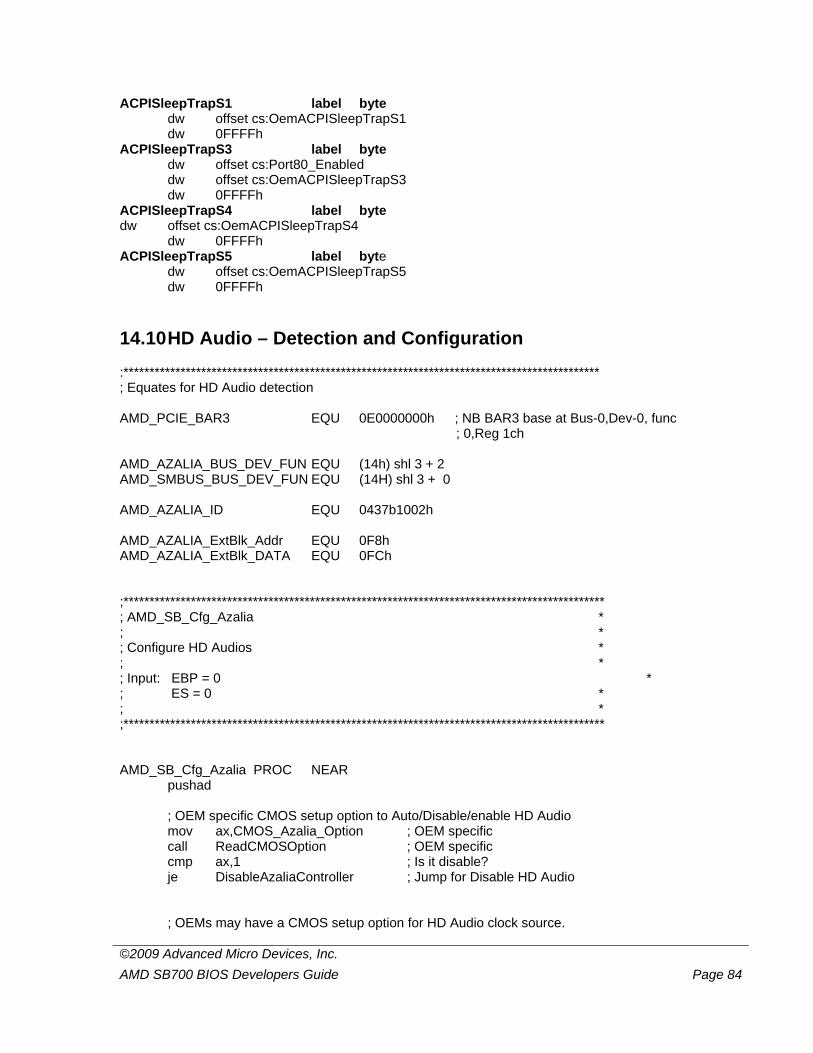
©2009 Advanced Micro Devices, Inc. AMD SB700 BIOS Developers Guide Page 84
ACPISleepTrapS1 label byte dw offset cs:OemACPISleepTrapS1 dw 0FFFFh
ACPISleepTrapS3 label byte dw offset cs:Port80_Enabled dw offset cs:OemACPISleepTrapS3 dw 0FFFFh
ACPISleepTrapS4 label byte dw offset cs:OemACPISleepTrapS4
dw 0FFFFh ACPISleepTrapS5 label byte
dw offset cs:OemACPISleepTrapS5 dw 0FFFFh
14.10 HD Audio – Detection and Configuration
:******************************************************************************************** ; Equates for HD Audio detection AMD_PCIE_BAR3 EQU 0E0000000h ; NB BAR3 base at Bus-0,Dev-0, func ; 0,Reg 1ch AMD_AZALIA_BUS_DEV_FUN EQU (14h) shl 3 + 2 AMD_SMBUS_BUS_DEV_FUN EQU (14H) shl 3 + 0 AMD_AZALIA_ID EQU 0437b1002h AMD_AZALIA_ExtBlk_Addr EQU 0F8h AMD_AZALIA_ExtBlk_DATA EQU 0FCh ;********************************************************************************************* ; AMD_SB_Cfg_Azalia * ; * ; Configure HD Audios * ; * ; Input: EBP = 0 * ; ES = 0 * ; * ;********************************************************************************************* AMD_SB_Cfg_Azalia PROC NEAR pushad ; OEM specific CMOS setup option to Auto/Disable/enable HD Audio mov ax,CMOS_Azalia_Option ; OEM specific call ReadCMOSOption ; OEM specific cmp ax,1 ; Is it disable? je DisableAzaliaController ; Jump for Disable HD Audio ; OEMs may have a CMOS setup option for HD Audio clock source.
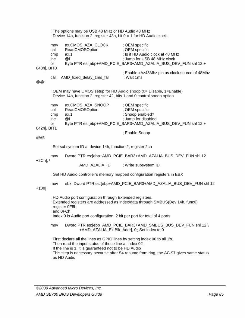
©2009 Advanced Micro Devices, Inc. AMD SB700 BIOS Developers Guide Page 85
; The options may be USB 48 MHz or HD Audio 48 MHz ; Device 14h, function 2, register 43h, bit 0 = 1 for HD Audio clock.
mov ax,CMOS_AZA_CLOCK ; OEM specific call ReadCMOSOption ; OEM specific cmp ax,1 ; Is it HD Audio clock at 48 MHz jne @f ; Jump for USB 48 MHz clock or Byte PTR es:[ebp+AMD_PCIE_BAR3+AMD_AZALIA_BUS_DEV_FUN shl 12 + 043h], BIT0 ; Enable xAz48Mhz pin as clock source of 48Mhz call AMD_fixed_delay_1ms_far ; Wait 1ms @@: ; OEM may have CMOS setup for HD Audio snoop (0= Disable, 1=Enable) ; Device 14h, function 2, register 42, bits 1 and 0 control snoop option mov ax,CMOS_AZA_SNOOP ; OEM specific call ReadCMOSOption ; OEM specific cmp ax,1 ; Snoop enabled? jne @f ; Jump for disabled or Byte PTR es:[ebp+AMD_PCIE_BAR3+AMD_AZALIA_BUS_DEV_FUN shl 12 + 042h], BIT1 ; Enable Snoop @@: ; Set subsystem ID at device 14h, function 2, register 2ch mov Dword PTR es:[ebp+AMD_PCIE_BAR3+AMD_AZALIA_BUS_DEV_FUN shl 12 +2Ch], \
AMD_AZALIA_ID ; Write subsystem ID ; Get HD Audio controller’s memory mapped configuration registers in EBX mov ebx, Dword PTR es:[ebp+AMD_PCIE_BAR3+AMD_AZALIA_BUS_DEV_FUN shl 12 +10h] ; HD Audio port configuration through Extended registers. ; Extended registers are addressed as index/data through SMBUS(Dev 14h, func0) ; register 0F8h,
; and 0FCh ; Index 0 is Audio port configuration. 2 bit per port for total of 4 ports
mov Dword PTR es:[ebp+AMD_PCIE_BAR3+AMD_SMBUS_BUS_DEV_FUN shl 12 \
+AMD_AZALIA_ExtBlk_Addr], 0 ; Set index to 0
; First declare all the lines as GPIO lines by setting index 00 to all 1's. ; Then read the input status of these line at index 02 ; If the line is 1, it is guaranteed not to be HD Audio ; This step is necessary because after S4 resume from ring, the AC-97 gives same status ; as HD Audio
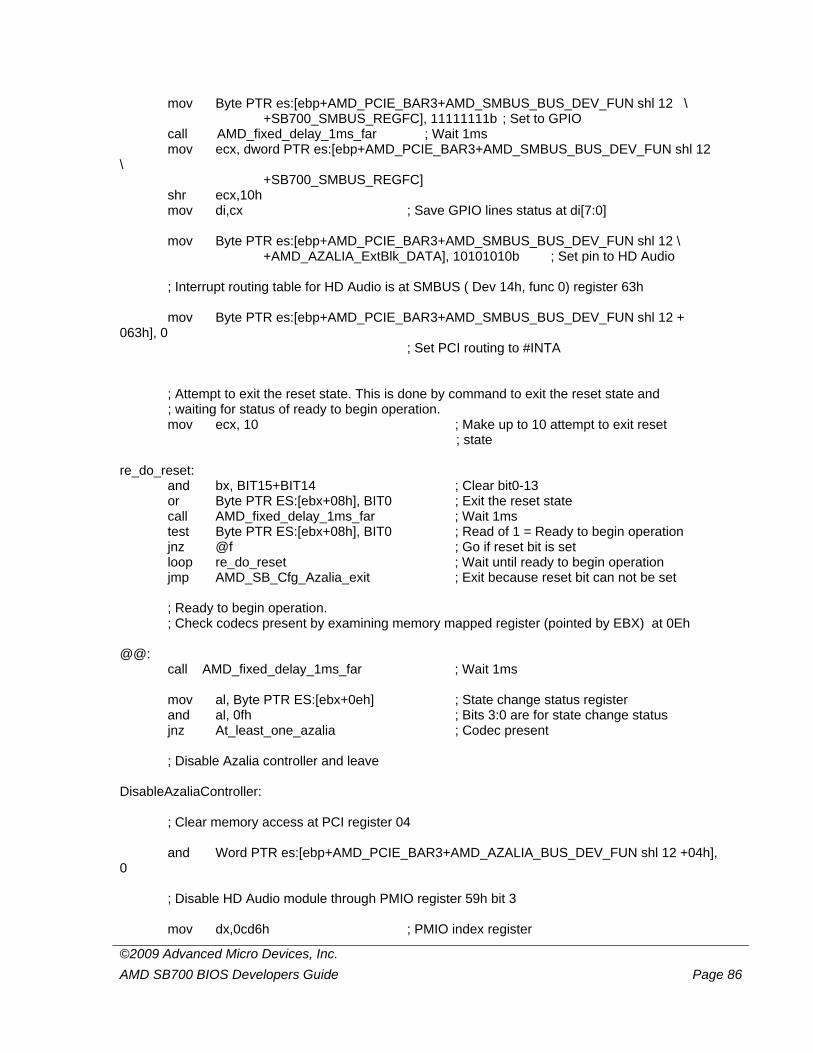
©2009 Advanced Micro Devices, Inc. AMD SB700 BIOS Developers Guide Page 86
mov Byte PTR es:[ebp+AMD_PCIE_BAR3+AMD_SMBUS_BUS_DEV_FUN shl 12 \ +SB700_SMBUS_REGFC], 11111111b ; Set to GPIO
call AMD_fixed_delay_1ms_far ; Wait 1ms mov ecx, dword PTR es:[ebp+AMD_PCIE_BAR3+AMD_SMBUS_BUS_DEV_FUN shl 12 \
+SB700_SMBUS_REGFC] shr ecx,10h mov di,cx ; Save GPIO lines status at di[7:0]
mov Byte PTR es:[ebp+AMD_PCIE_BAR3+AMD_SMBUS_BUS_DEV_FUN shl 12 \
+AMD_AZALIA_ExtBlk_DATA], 10101010b ; Set pin to HD Audio
; Interrupt routing table for HD Audio is at SMBUS ( Dev 14h, func 0) register 63h
mov Byte PTR es:[ebp+AMD_PCIE_BAR3+AMD_SMBUS_BUS_DEV_FUN shl 12 + 063h], 0 ; Set PCI routing to #INTA ; Attempt to exit the reset state. This is done by command to exit the reset state and ; waiting for status of ready to begin operation. mov ecx, 10 ; Make up to 10 attempt to exit reset ; state re_do_reset: and bx, BIT15+BIT14 ; Clear bit0-13 or Byte PTR ES:[ebx+08h], BIT0 ; Exit the reset state call AMD_fixed_delay_1ms_far ; Wait 1ms test Byte PTR ES:[ebx+08h], BIT0 ; Read of 1 = Ready to begin operation jnz @f ; Go if reset bit is set loop re_do_reset ; Wait until ready to begin operation jmp AMD_SB_Cfg_Azalia_exit ; Exit because reset bit can not be set ; Ready to begin operation. ; Check codecs present by examining memory mapped register (pointed by EBX) at 0Eh @@: call AMD_fixed_delay_1ms_far ; Wait 1ms mov al, Byte PTR ES:[ebx+0eh] ; State change status register and al, 0fh ; Bits 3:0 are for state change status jnz At_least_one_azalia ; Codec present
; Disable Azalia controller and leave
DisableAzaliaController:
; Clear memory access at PCI register 04 and Word PTR es:[ebp+AMD_PCIE_BAR3+AMD_AZALIA_BUS_DEV_FUN shl 12 +04h], 0 ; Disable HD Audio module through PMIO register 59h bit 3 mov dx,0cd6h ; PMIO index register
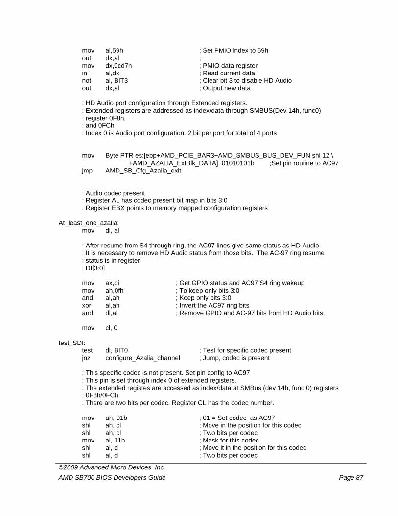
©2009 Advanced Micro Devices, Inc. AMD SB700 BIOS Developers Guide Page 87
mov al,59h ; Set PMIO index to 59h out dx,al ; mov dx,0cd7h ; PMIO data register in al,dx ; Read current data not al, BIT3 ; Clear bit 3 to disable HD Audio out dx,al ; Output new data ; HD Audio port configuration through Extended registers. ; Extended registers are addressed as index/data through SMBUS(Dev 14h, func0) ; register 0F8h,
; and 0FCh ; Index 0 is Audio port configuration. 2 bit per port for total of 4 ports
mov Byte PTR es:[ebp+AMD_PCIE_BAR3+AMD_SMBUS_BUS_DEV_FUN shl 12 \
+AMD_AZALIA_ExtBlk_DATA], 01010101b ;Set pin routine to AC97 jmp AMD_SB_Cfg_Azalia_exit ; Audio codec present ; Register AL has codec present bit map in bits 3:0 ; Register EBX points to memory mapped configuration registers At_least_one_azalia: mov dl, al ; After resume from S4 through ring, the AC97 lines give same status as HD Audio
; It is necessary to remove HD Audio status from those bits. The AC-97 ring resume ; status is in register ; DI[3:0]
mov ax,di ; Get GPIO status and AC97 S4 ring wakeup mov ah,0fh ; To keep only bits 3:0 and al,ah ; Keep only bits 3:0 xor al,ah ; Invert the AC97 ring bits and dl,al ; Remove GPIO and AC-97 bits from HD Audio bits mov cl, 0 test_SDI: test dl, BIT0 ; Test for specific codec present jnz configure_Azalia_channel ; Jump, codec is present
; This specific codec is not present. Set pin config to AC97 ; This pin is set through index 0 of extended registers. ; The extended registes are accessed as index/data at SMBus (dev 14h, func 0) registers
; 0F8h/0FCh ; There are two bits per codec. Register CL has the codec number.
mov ah, 01b ; 01 = Set codec as AC97 shl ah, cl ; Move in the position for this codec shl ah, cl ; Two bits per codec mov al, 11b ; Mask for this codec shl al, cl ; Move it in the position for this codec shl al, cl ; Two bits per codec
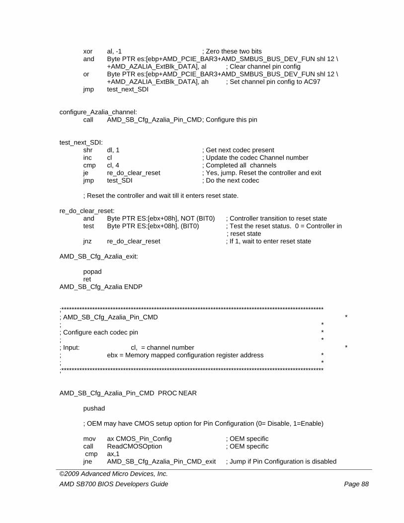
©2009 Advanced Micro Devices, Inc. AMD SB700 BIOS Developers Guide Page 88
xor al, -1 ; Zero these two bits and Byte PTR es:[ebp+AMD_PCIE_BAR3+AMD_SMBUS_BUS_DEV_FUN shl 12 \
+AMD_AZALIA_ExtBlk_DATA], al ; Clear channel pin config or Byte PTR es:[ebp+AMD_PCIE_BAR3+AMD_SMBUS_BUS_DEV_FUN shl 12 \
+AMD_AZALIA_ExtBlk_DATA], ah ; Set channel pin config to AC97 jmp test_next_SDI configure_Azalia_channel: call AMD_SB_Cfg_Azalia_Pin_CMD ; Configure this pin test_next_SDI: shr dl, 1 ; Get next codec present inc cl ; Update the codec Channel number cmp cl, 4 ; Completed all channels je re_do_clear_reset ; Yes, jump. Reset the controller and exit jmp test_SDI ; Do the next codec ; Reset the controller and wait till it enters reset state. re_do_clear_reset: and Byte PTR ES:[ebx+08h], NOT (BIT0) ; Controller transition to reset state test Byte PTR ES:[ebx+08h], (BIT0) ; Test the reset status. 0 = Controller in ; reset state jnz re_do_clear_reset ; If 1, wait to enter reset state AMD_SB_Cfg_Azalia_exit: popad ret AMD_SB_Cfg_Azalia ENDP ;****************************************************************************************************** ; AMD_SB_Cfg_Azalia_Pin_CMD * ; * ; Configure each codec pin * ; * ; Input: cl, = channel number * ; ebx = Memory mapped configuration register address * ; * ;****************************************************************************************************** AMD_SB_Cfg_Azalia_Pin_CMD PROC NEAR pushad
; OEM may have CMOS setup option for Pin Configuration (0= Disable, 1=Enable) mov ax CMOS_Pin_Config ; OEM specific call ReadCMOSOption ; OEM specific cmp ax,1
jne AMD_SB_Cfg_Azalia_Pin_CMD_exit ; Jump if Pin Configuration is disabled
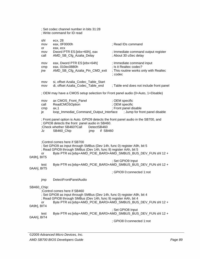
©2009 Advanced Micro Devices, Inc. AMD SB700 BIOS Developers Guide Page 89
; Set codec channel number in bits 31:28 ; Write command for ID read shl ecx, 28 mov eax, 0F0000h ; Read IDs command or eax, ecx mov Dword PTR ES:[ebx+60h], eax ; Immediate command output register call AMD_SB_Cfg_Azalia_Delay ; About 30 uSec delay mov eax, Dword PTR ES:[ebx+64h] ; Immediate command input cmp eax, 010ec0880h ; Is it Realtec codec? jne AMD_SB_Cfg_Azalia_Pin_CMD_exit ; This routine works only with Realtec ; codec mov si, offset Azalia_Codec_Table_Start mov di, offset Azalia_Codec_Table_end ; Table end does not include front panel ; OEM may have a CMOS setup selection for Front panel audio (0=Auto, 1=Disable)
mov ax CMOS_Front_Panel ; OEM specific call ReadCMOSOption ; OEM specific
cmp ax,1 ; Front panel disable je loop_Immediat_Command_Output_Interface ; Jump for front panel disable
; Front panel option is Auto. GPIO9 detects the front panel audio in the SB700, and ; GPIO8 detects the front panel audio in SB460.
;Check whether SB460?Call DetectSB460 Jz SB460_Chip ;jmp if SB460 ;Control comes here if SB700
; Set GPIO9 as input through SMBus (Dev 14h, func 0) register A9h, bit 5 ; Read GPIO9 through SMBus (Dev 14h, func 9) register AAh, bit 5 or Byte PTR es:[ebp+AMD_PCIE_BAR3+AMD_SMBUS_BUS_DEV_FUN shl 12 + 0A9h], BIT5 ; Set GPIO9 Input test Byte PTR es:[ebp+AMD_PCIE_BAR3+AMD_SMBUS_BUS_DEV_FUN shl 12 + 0AAh], BIT5 ; GPIO9 0:connected 1:not jmp DetectFrontPanelAudio SB460_Chip:
;Control comes here if SB460 ; Set GPIO8 as input through SMBus (Dev 14h, func 0) register A9h, bit 4 ; Read GPIO8 through SMBus (Dev 14h, func 9) register AAh, bit 4 or Byte PTR es:[ebp+AMD_PCIE_BAR3+AMD_SMBUS_BUS_DEV_FUN shl 12 + 0A9h], BIT4 ; Set GPIO8 Input test Byte PTR es:[ebp+AMD_PCIE_BAR3+AMD_SMBUS_BUS_DEV_FUN shl 12 + 0AAh], BIT4 ; GPIO8 0:connected 1:not
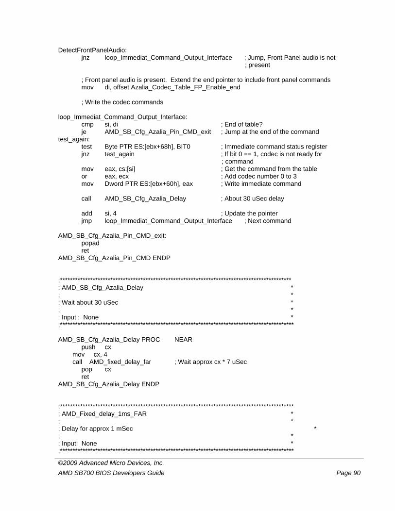
©2009 Advanced Micro Devices, Inc. AMD SB700 BIOS Developers Guide Page 90
DetectFrontPanelAudio: jnz loop_Immediat_Command_Output_Interface ; Jump, Front Panel audio is not ; present ; Front panel audio is present. Extend the end pointer to include front panel commands mov di, offset Azalia_Codec_Table_FP_Enable_end ; Write the codec commands loop_Immediat_Command_Output_Interface: cmp si, di ; End of table? je AMD_SB_Cfg_Azalia_Pin_CMD_exit ; Jump at the end of the command test_again: test Byte PTR ES:[ebx+68h], BIT0 ; Immediate command status register jnz test_again ; If bit 0 == 1, codec is not ready for ; command mov eax, cs:[si] ; Get the command from the table or eax, ecx ; Add codec number 0 to 3 mov Dword PTR ES:[ebx+60h], eax ; Write immediate command call AMD_SB_Cfg_Azalia_Delay ; About 30 uSec delay add si, 4 ; Update the pointer jmp loop_Immediat_Command_Output_Interface ; Next command AMD_SB_Cfg_Azalia_Pin_CMD_exit: popad ret AMD_SB_Cfg_Azalia_Pin_CMD ENDP ;******************************************************************************************** : AMD_SB_Cfg_Azalia_Delay * ; * ; Wait about 30 uSec * ; * : Input : None * ;********************************************************************************************* AMD_SB_Cfg_Azalia_Delay PROC NEAR push cx mov cx, 4 call AMD_fixed_delay_far ; Wait approx cx * 7 uSec pop cx ret AMD_SB_Cfg_Azalia_Delay ENDP ;********************************************************************************************* ; AMD_Fixed_delay_1ms_FAR * ; * ; Delay for approx 1 mSec * ; * ; Input: None * ;*********************************************************************************************
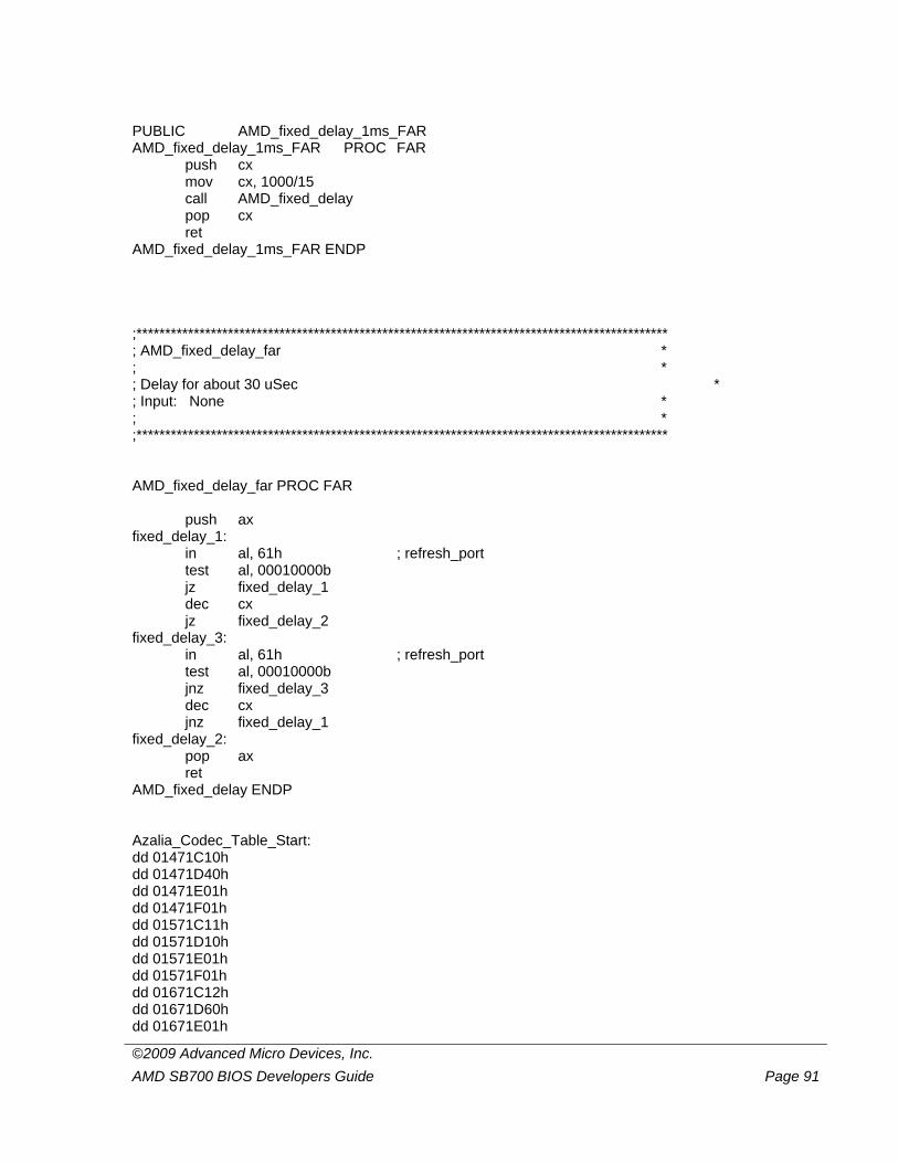
©2009 Advanced Micro Devices, Inc. AMD SB700 BIOS Developers Guide Page 91
PUBLIC AMD_fixed_delay_1ms_FAR AMD_fixed_delay_1ms_FAR PROC FAR push cx mov cx, 1000/15 call AMD_fixed_delay pop cx ret AMD_fixed_delay_1ms_FAR ENDP ;********************************************************************************************* ; AMD_fixed_delay_far * ; * ; Delay for about 30 uSec * ; Input: None * ; * ;********************************************************************************************* AMD_fixed_delay_far PROC FAR push ax fixed_delay_1: in al, 61h ; refresh_port test al, 00010000b jz fixed_delay_1 dec cx jz fixed_delay_2 fixed_delay_3: in al, 61h ; refresh_port test al, 00010000b jnz fixed_delay_3 dec cx jnz fixed_delay_1 fixed_delay_2: pop ax ret AMD_fixed_delay ENDP Azalia_Codec_Table_Start: dd 01471C10h dd 01471D40h dd 01471E01h dd 01471F01h dd 01571C11h dd 01571D10h dd 01571E01h dd 01571F01h dd 01671C12h dd 01671D60h dd 01671E01h
©2009 Advanced Micro Devices, Inc. AMD SB700 BIOS Developers Guide Page 92
dd 01671F01h dd 01771C13h dd 01771D20h dd 01771E01h dd 01771F01h dd 01871C30h dd 01871D91h dd 01871Ea1h dd 01871F01h dd 01971C00h dd 01971D00h dd 01971E00h dd 01971F40h dd 01a71C31h dd 01a71D31h dd 01a71E81h dd 01a71F01h dd 01b71C00h dd 01b71D00h dd 01b71E00h dd 01b71F40h dd 01c71C70h dd 01c71D10h dd 01c71E33h dd 01c71F99h dd 01d71C00h dd 01d71D10h dd 01d71E7fh dd 01d71F90h dd 01e71C50h dd 01e71D00h dd 01e71E44h dd 01e71F01h dd 01f71C60h dd 01f71D00h dd 01f71Ec4h dd 01f71F01h Azalia_Codec_Table_end: dd 01971C20h dd 01971D91h dd 01971E21h dd 01971F02h dd 01B71C40h dd 01B71D41h dd 01B71EA1h dd 01B71F02h Azalia_Codec_Table_FP_Enable_end:
©2009 Advanced Micro Devices, Inc. AMD SB700 BIOS Developers Guide Page 93
15 Chipset Integration Module Extensive (SB700 CIMx)
15.1 Introduction
CIMx-SB7xx introduces a new interface and distribution model to help quickly integrate SB7xx (SB700/SB710/SB750) Southbridge family support in the customer products.
15.2 Distribution Model
To avoid miscellaneous build issues and simplify integration with different BIOS code bases, CIMx-SB7xx is distributed in the form of binary files called “B1” and “B2”. B1 contains minimum initialization required for BIOS recovery, while B2 contains full chipset initialization code.
15.3 CIMx Architecture
CIMx is completely re-architected from the previous generation of CIM code. CIMx release contains two binary files (B1 and B2). B1 image must be integrated in the boot block part of the BIOS in uncompressed form to ensure possibility of recovery if the main bios image is corrupted. There are no restrictions on B2 location. B2 image should be integrated in the main BIOS in uncompressed form. B1 contains the minimal chipset initialization required for boot block recovery. B2 supports the complete chipset initialization which is required for normal BIOS post. During power on, the boot block BIOS code should call the B1 module to do the power on settings required for the chipset. Boot block BIOS code can inform the B1 module the location of the B2 module and whether B1 module is allowed to call the B2 module. If the B2 module location is not given as input, B1 can search for the B2 module. Once the B1 module finds the B2 module, it validates the B2 module, and if valid, passes the call to B2 module if the boot block BIOS allows it to do so. If the B2 module is invalid or if boot bblock BIOS doesn’t allow B1 to call B2, then B1 module services the call itself. Since B1 module searches the ROM for B2 module, B2 module should be integrated into the BIOS as uncompressed. Also to speed up the search for B2 module, B2 module should be integrated in 32K Byte alignment. B1 & B2 modules should be given control in 32-bit flat protected mode with both DS, ES & SS set to 0-4GB flat mode descriptors. B1 & B2 can be executed from ROM or by copying to memory with cache enabled. Cache needs to be enabled for the modules to be executed in ROM. CIMx code is mostly written in ‘C’ in order to be compatible with both legacy BIOS and EFI environments. Figure 5 shows the flow of system BIOS which has integrated the CIMx modules to support AMD chipsets.
©2009 Advanced Micro Devices, Inc. AMD SB700 BIOS Developers Guide Page 94
Power on Reset
Notrhbridge HT Initialization
CIMx-SB7xx POR Init
Memory detection.System BIOS shadowing
Is S3 Resume
Restore Memory Controller
Restore PCI Device configuration space
Misc. Restore CPU
Norhbridge S3 initialization
Misc BIOS restore.Give control to OS
Operatin System
Notrhbridge Start Post Initialization
CIMx-SB7xx - InitSBeforePciEnum
PCI enumeration and resource allocation
Video BIOS call
CIMx-SB7xx - InitSBAfterPciEnum
Cnfigure all IO device.Enumerate USB.Detect and initialize all boot devices.Initialize and execute Option ROM.BIOS setup, etc
Norhbridge late Post initialization
YesNo
CIMx-SB7xx - InitSbBfPciRestore
CIMx-SB7xx - InitSbAfPciRestore
HT Initialization
Warm Reset Required ?
Notrhbridge Power On Initialization
Norhbridge PCIE S3 initialization
Yes
No
CIMx-SB7xx - LatePostInitialization
Figure 5 Flowchart of SBIOS with Integrated CIMx
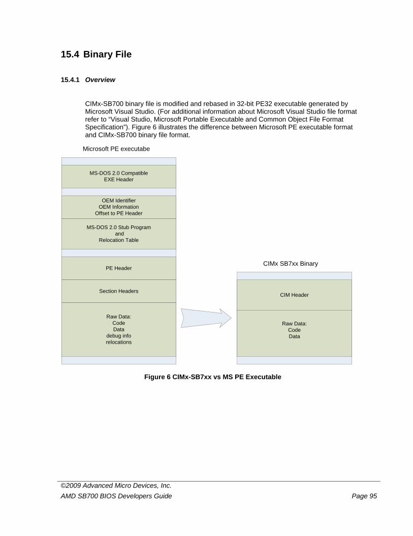
©2009 Advanced Micro Devices, Inc. AMD SB700 BIOS Developers Guide Page 95
15.4 Binary File
15.4.1 Overview
CIMx-SB700 binary file is modified and rebased in 32-bit PE32 executable generated by Microsoft Visual Studio. (For additional information about Microsoft Visual Studio file format refer to “Visual Studio, Microsoft Portable Executable and Common Object File Format Specification”). Figure 6 illustrates the difference between Microsoft PE executable format and CIMx-SB700 binary file format.
MS-DOS 2.0 CompatibleEXE Header
OEM IdentifierOEM Information
Offset to PE Header
PE Header
Section Headers
MS-DOS 2.0 Stub Program and
Relocation Table
Microsoft PE executabe
Raw Data:CodeData
CIM Header
CIMx SB7xx Binary
Raw Data:CodeData
debug inforelocations
Figure 6 CIMx-SB7xx vs MS PE Executable
©2009 Advanced Micro Devices, Inc. AMD SB700 BIOS Developers Guide Page 96
15.4.2 Binary Header
The CIMx-SB700 consists of file header followed immediately by Raw Code and Data. Table 2 CIMx File Header Definition Offset Size Field Description 0 4 Signature Signature that identifies this as a CIMx
module 4 4 EntryPointAddress Address of the entry point relevant to the
beginning of the binary image. 8 4 ModuleSignature Signature that identify this particular
CIMx module. 12 4 ImageSize Size in number of bytes of complete binary
including the header. 16 2 ModuleVersion Version of the binary module. 16 2 Checksum Checksum of the binary image. 18 5 Reserved Space reserved for future use.
15.5 CIMx Interface Calls Environment
Prior to calling any CIMX interface, it is required that: 1. Place CPU into 32 bit protected mode. 2. Set CS as 32bit code segment with Base/Limit – 0x00000000/0xffffffff. 3. Set DS/ES/SS as 32bit data segment with Base/Limit – 0x00000000/0xffffffff. See Example.
15.6 Interface Definition
All interface calls to CIMx-SB700 binary are C like calls to the Entry Point of the binary image. void (*ImageEntryPointPtr)(void* Config)
15.6.1 Southbridge Power-On/Reset Initialization
Upon system power-on, or cold reset, there is minimal initialization required like SMBus base address programming, enabling the legacy IO (like port 60/64 etc) decoding etc to bring the system to a working state. BIOS should call this entry to B1 module at very early stage during power on initialization. CIMx has assumed a set of default values for all the build parameters such as bios size, smbus base address, power management base addresses etc. If you wan to use your own set of values for these configurable options, then you can define the buildparameters structure and give the 32bit physical pointer as input to the CIMx module. If the pointer is NULL or set to all 1, then the CIMx module uses the default parameters which are built. Also
©2009 Advanced Micro Devices, Inc. AMD SB700 BIOS Developers Guide Page 97
the bios developer has the flexibility of changing the oem.h file to redefine the values but in this, the CIMx module needs to be rebuilt for the new values to be included in the binary.
Functions Documentation
void (*ImageEntryPointPtr)(AMDSBCFGBB* Config) Parameters typedef struct _AMDSBCFGBB { STDCFG StdHeader; //offset 0:16 - 17 bytes UINT32 MsgXchgBiosCimxBB; //offset 17:20 - 4 bytes BUILDPARAM *BuildParametersPtr; //offset 21:24 - 4 bytes }AMDSBCFGBB; Detail Description stdHeader – Standard function call
stdHeader.Func = 0x01. typedef struct _STDCFG{ UINT32 pImageBase; UINT32 pPcieBase; UINT8 Func; UINT32 pCallBack; UINT32 pB2ImageBase; }STDCFG;
pImageBase - Physical address of binary image. pPcieBase - Address of PCIE Extended configuration space MMIO. Func – Function identifier. pCallBack - Address of OEM call back function pB2ImageBase – Optional parameter. Physical address of “B2” image.
MsgXchgBiosCimx – Field to exchange message between BIOS & CIMx
Bit Field Description [0] S3Resume Informs the CIMx module whether the
system is resuming from S3 [1] RebootRequired CIMx informs BIOS whether a reboot
is required after returning from CIMx call. Some internal clock settings and spread spectrum settings require a reboot.
[2] Spi33Mhz 0 – Leave the SPI ROM to default speed(16.5MHz) 1 – Bump up the SPI ROM to 33Mhz.
©2009 Advanced Micro Devices, Inc. AMD SB700 BIOS Developers Guide Page 98
Bit Field Description [3] SpreadSpectrum When using external clock
0 – Disable SB internal spread spectrum on sb pci clocks 1 – Enable SB internal spread specturm on pci clks. (If this option is enabled and if the clock input to SB is already spread, then it will cause double spread on the SB pci clks). When using internal clock boards 0 – Disable SB internal spread spectrum. 1 – Enable SB internal spread specturm on clocks going out from SB. (if this option is enable, then it will enable spread on all clocks except USB, SATA and DISP clocks).
[4] UsbIntClock 0 – Use external 48MHz clock source for usb controllers. 1 – Use SB700 internal clock source for usb controllers
[5] PciClk5 0 – Leave PCIClk5 pin as GPIO 1 – Enable PCIClk5 pin as PCI CLK.
[7:6] TimerClockSource This option is applicable only for SB700-A13, SB710 & SB700S. 0 – 100Mhz PCIE Reference clock, Use 100Mhz PCIE reference clock as timer clock source to SB (compatible with SB700-A12). 1 – 14Mhz using 25M_48M_66M_OSC pin, , Use external 14Mhz clock source for system timer clock by routing 25M_X1 pin directly into the internal clock. In the platform, 25M_X1 pin should be connected to 14Mhz clock source for this option.2 – Auto. If SB700 A12, use 100 Mhz PCIE reference clock. If SB700 A14, use external 14Mhz clock source by routing 25M_X1 pin directly into the internal clock.
[8] A13ECOs This option is to disable the SB700 A13 ECOs just for testing/debugging purposes. In general A13 ECOs should always be enabled. 0 – Enable A13 ECOs. 1 – Disable A13 ECOs. In future this option will be removed and A13 ECOs will always be enabled.
[31:9] MsgXchgBiosCimxDummyBB Dummy place holder for future use
©2009 Advanced Micro Devices, Inc. AMD SB700 BIOS Developers Guide Page 99
BuildParametersPtr – This is pointer to build parameter structure. It should point to the following structure (BUILDPARAM) or should be 0xFFFFFFFF and in that case CIMx will use the default structure. CIMx also provides the flexibility of changing the default build structure parameters by editing them in oem.h file. In the case CIMx module need to rebuilt so that the new parameters are updated. So there are basically three options.
1. Build parameters can be given as input by providing a pointer to BUILDPARAM structure as input.
2. OEM can use the default structure built into the binary by providing a NULL pointer as input.
3. OEM can change the values of default structure by updating them in oem.h file and use the updated default structure. In this case a NULL pointer should be provided as input. In this case, OEM needs to rebuild the CIMx module to have the binary updated with the new values.
typedef struct _BUILDPARAMBB { UINT16 BiosSize:3; //0-128KB, 1-256KB, 2-512KB, 4-1MB,.... UINT16 LegacyFree:1; UINT16 Dummy0:12; UINT16 EcKbd:1; UINT16 EcChannel0:1; UINT16 Dummy1:14; UINT32 Smbus0BaseAddress; UINT16 Smbus1BaseAddress; UINT32 SioPmeBaseAddress; UINT32 WatchDogTimerBase; UINT32 SpiRomBaseAddress; UINT16 AcpiPm1EvtBlkAddr; UINT16 AcpiPm1CntBlkAddr; UINT16 AcpiPmTmrBlkAddr; UINT16 CpuControlBlkAddr; UINT16 AcpiGpe0BlkAddr; UINT16 SmiCmdPortAddr; UINT16 AcpiPmaCntBlkAddr; UINT16 EcLdn5MailBoxAddr; UINT8 EcLdn5Irq; UINT16 EcLdn9MailBoxAddr; UINT32 ReservedDword0; UINT32 ReservedDword1; UINT32 ReservedDword2; UINT32 ReservedDword3; }BUILDPARAMBB; BiosSize – Size of the BIOS ROM(0-128KB, 1-256KB, 2-512KB, 4-1MB, 5-2MB, 6-4MB, Others: Reserved)
©2009 Advanced Micro Devices, Inc. AMD SB700 BIOS Developers Guide Page 100
LegacyFree – Indicates whether the system is Legacy Free ( 0 – Not Legacy Free, 1 – Legacy Free) Dummy0 – Dummy place holder for future use EcKbd – Indicates whether CIMx needs to enable the KBC in the EC EcChannel0– Indicates whether CIMx needs to enable the Channel0 in the EC Dummy1 – Dummy place holder for future use Smbus0BaseAddress – Base Address of SMBus 0. Smbus1BaseAddress – Base Address of SMBus 1. SioPmeBaseAddress – SIO PME Base Address to enable decoding of this address in LPC Bus. This is not used if system is legacy free. WatchDogTimerBase – WatchDog Timer Base Address. SpiRomBaseAddress – SPI ROM Base Address.
AcpiPm1EvtBlkAddr – ACPI Power management Event block address AcpiPm1CntBlkAddr – ACPI Power management Control block address AcpiPmTmrBlkAddr – ACPI Power management Timer block address CpuControlBlkAddr – ACPI Power management CPU Control block address AcpiGpe0BlkAddr – ACPI Power management General Purpose Event block address SmiCmdPortAddr – ACPI Power management SMI Command block address AcpiPmaCntBlkAddr – ACPI Power management Additional control block address EcLdn5MailBoxAddr – EC Logical Device 5 Mailbox base address. EcLdn5Irq – Interrupt to be assigned to EC Logical Device 5. EcLdn9MailBoxAddr – EC Logical Device 9 Mailbox base address. ReservedDword0 – Reserved for future use. ReservedDword1 – Reserved for future use. ReservedDword2 – Reserved for future use. ReservedDword3 – Reserved for future use.
©2009 Advanced Micro Devices, Inc. AMD SB700 BIOS Developers Guide Page 101
15.6.2 SouthBridge BIOS Post Initialization
SB700 BIOS post initialization is divided into 3 stages as before pci enumeration, after pci enumeration and late post initialization. All these 3 calls need the same inputs except that the function id should be setup properly. “Before pci enumeration” routine should be called before pci devices are enumerated and resources are assigned. It is recommended to call the pci before initialization at very early post after memory detection. “After pci enumeration routine” should be called after the resources are assigned to the pci devices since this routine initializes MMIO spaces of some of the devices. Late post initialization should be called at the end of BIOS post just before giving control to OS. Functions Documentation
void (*ImageEntryPointPtr)(AMDSBCFG* Config) Parameters typedef struct _AMDSBCFG { STDCFG StdHeader; UINT32 MsgXchgBiosCimx; BUILDPARAM *BuildParametersPtr; UINT32 SataConfiguration; UINT16 FCConfig; UINT16 UsbConfiguration; UINT32 AzaliaConfiguration; CODECTBLLIST* pAzaliaOemCodecTablePtr; UINT32 pAzaliaOemFpCodecTableptr; UINT32 MiscConfiguration; UINT32 AsmAslInfoExchange0; UINT32 AsmAslInfoExchange1; UINT32 DebugOptions_1; UINT32 DebugOptions_2; UINT32 TempMMIO }AMDSBCFG; Detail Description stdHeader – Standard function call (see STDCFG definition)
stdHeader.Func = 0x10 – Before PCI enumeration init stdHeader.Func = 0x20 – After PCI enumeration init stdHeader.Func = 0x30 – Late post init
MsgXchgBiosCimx – Field to exchange message between BIOS & CIMx
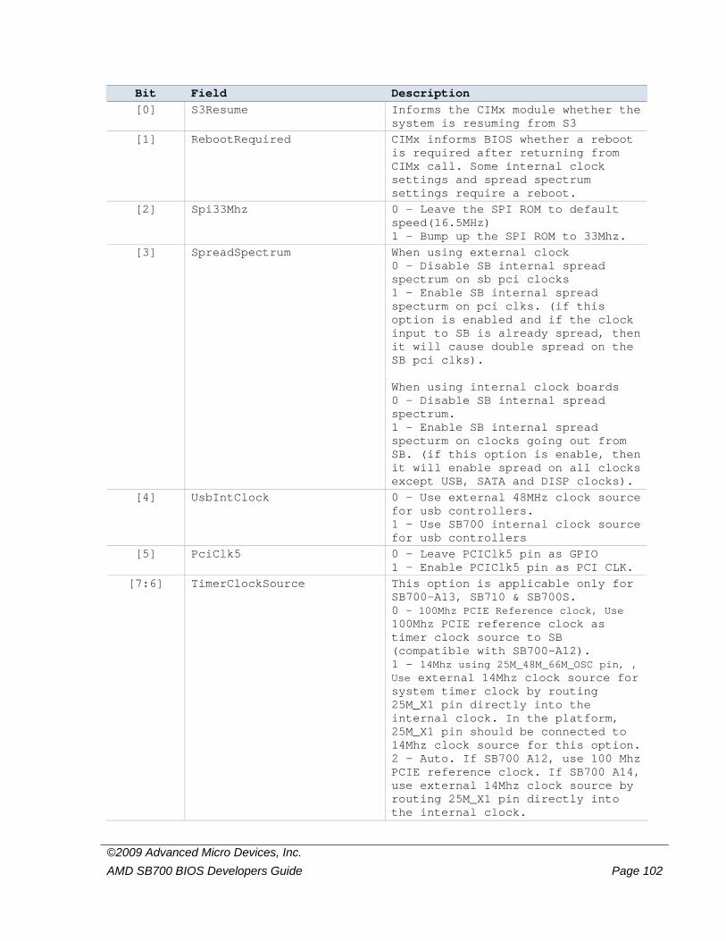
©2009 Advanced Micro Devices, Inc. AMD SB700 BIOS Developers Guide Page 102
Bit Field Description [0] S3Resume Informs the CIMx module whether the
system is resuming from S3 [1] RebootRequired CIMx informs BIOS whether a reboot
is required after returning from CIMx call. Some internal clock settings and spread spectrum settings require a reboot.
[2] Spi33Mhz 0 – Leave the SPI ROM to default speed(16.5MHz) 1 – Bump up the SPI ROM to 33Mhz.
[3] SpreadSpectrum When using external clock 0 – Disable SB internal spread spectrum on sb pci clocks 1 – Enable SB internal spread specturm on pci clks. (if this option is enabled and if the clock input to SB is already spread, then it will cause double spread on the SB pci clks). When using internal clock boards 0 – Disable SB internal spread spectrum. 1 – Enable SB internal spread specturm on clocks going out from SB. (if this option is enable, then it will enable spread on all clocks except USB, SATA and DISP clocks).
[4] UsbIntClock 0 – Use external 48MHz clock source for usb controllers. 1 – Use SB700 internal clock source for usb controllers
[5] PciClk5 0 – Leave PCIClk5 pin as GPIO 1 – Enable PCIClk5 pin as PCI CLK.
[7:6] TimerClockSource This option is applicable only for SB700-A13, SB710 & SB700S. 0 – 100Mhz PCIE Reference clock, Use 100Mhz PCIE reference clock as timer clock source to SB (compatible with SB700-A12). 1 – 14Mhz using 25M_48M_66M_OSC pin, , Use external 14Mhz clock source for system timer clock by routing 25M_X1 pin directly into the internal clock. In the platform, 25M_X1 pin should be connected to 14Mhz clock source for this option.2 – Auto. If SB700 A12, use 100 Mhz PCIE reference clock. If SB700 A14, use external 14Mhz clock source by routing 25M_X1 pin directly into the internal clock.
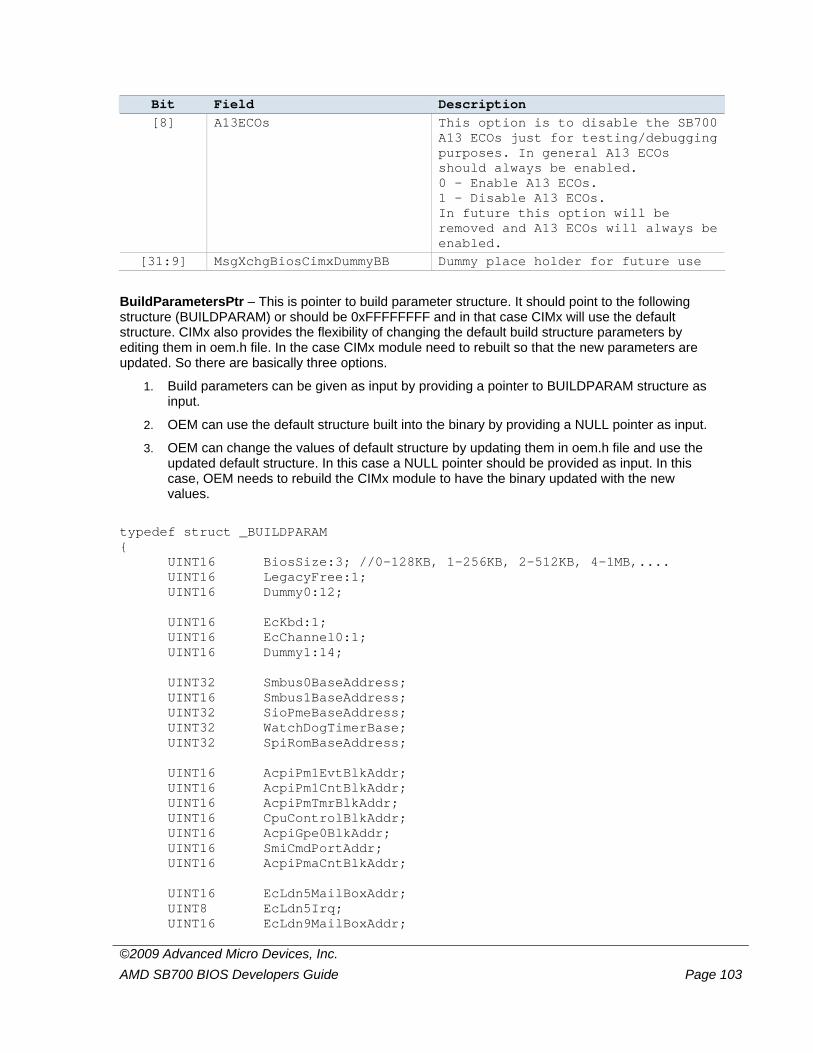
©2009 Advanced Micro Devices, Inc. AMD SB700 BIOS Developers Guide Page 103
Bit Field Description [8] A13ECOs This option is to disable the SB700
A13 ECOs just for testing/debugging purposes. In general A13 ECOs should always be enabled. 0 – Enable A13 ECOs. 1 – Disable A13 ECOs. In future this option will be removed and A13 ECOs will always be enabled.
[31:9] MsgXchgBiosCimxDummyBB Dummy place holder for future use
BuildParametersPtr – This is pointer to build parameter structure. It should point to the following structure (BUILDPARAM) or should be 0xFFFFFFFF and in that case CIMx will use the default structure. CIMx also provides the flexibility of changing the default build structure parameters by editing them in oem.h file. In the case CIMx module need to rebuilt so that the new parameters are updated. So there are basically three options.
1. Build parameters can be given as input by providing a pointer to BUILDPARAM structure as input.
2. OEM can use the default structure built into the binary by providing a NULL pointer as input.
3. OEM can change the values of default structure by updating them in oem.h file and use the updated default structure. In this case a NULL pointer should be provided as input. In this case, OEM needs to rebuild the CIMx module to have the binary updated with the new values.
typedef struct _BUILDPARAM { UINT16 BiosSize:3; //0-128KB, 1-256KB, 2-512KB, 4-1MB,.... UINT16 LegacyFree:1; UINT16 Dummy0:12; UINT16 EcKbd:1; UINT16 EcChannel0:1; UINT16 Dummy1:14; UINT32 Smbus0BaseAddress; UINT16 Smbus1BaseAddress; UINT32 SioPmeBaseAddress; UINT32 WatchDogTimerBase; UINT32 SpiRomBaseAddress; UINT16 AcpiPm1EvtBlkAddr; UINT16 AcpiPm1CntBlkAddr; UINT16 AcpiPmTmrBlkAddr; UINT16 CpuControlBlkAddr; UINT16 AcpiGpe0BlkAddr; UINT16 SmiCmdPortAddr; UINT16 AcpiPmaCntBlkAddr; UINT16 EcLdn5MailBoxAddr; UINT8 EcLdn5Irq; UINT16 EcLdn9MailBoxAddr;
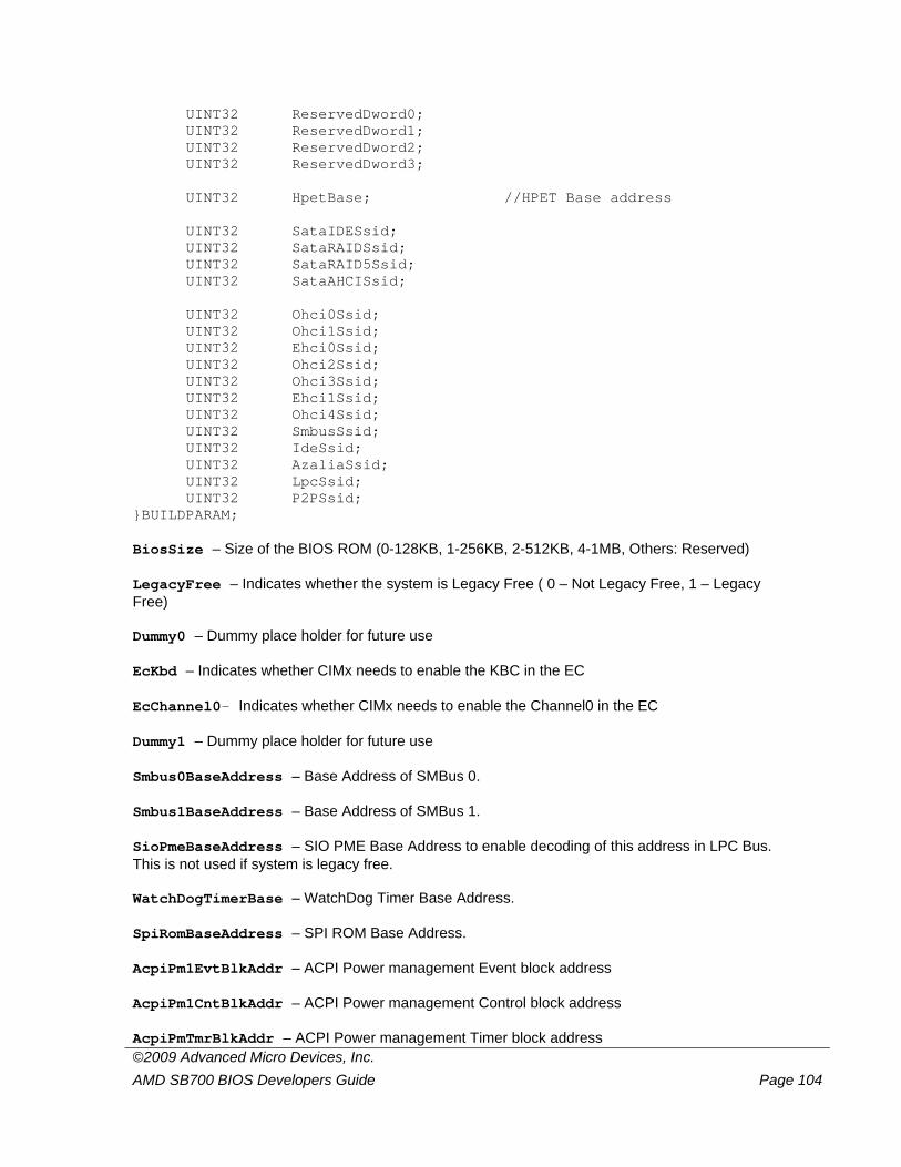
©2009 Advanced Micro Devices, Inc. AMD SB700 BIOS Developers Guide Page 104
UINT32 ReservedDword0; UINT32 ReservedDword1; UINT32 ReservedDword2; UINT32 ReservedDword3; UINT32 HpetBase; //HPET Base address UINT32 SataIDESsid; UINT32 SataRAIDSsid; UINT32 SataRAID5Ssid; UINT32 SataAHCISsid; UINT32 Ohci0Ssid; UINT32 Ohci1Ssid; UINT32 Ehci0Ssid; UINT32 Ohci2Ssid; UINT32 Ohci3Ssid; UINT32 Ehci1Ssid; UINT32 Ohci4Ssid; UINT32 SmbusSsid; UINT32 IdeSsid; UINT32 AzaliaSsid; UINT32 LpcSsid; UINT32 P2PSsid; }BUILDPARAM; BiosSize – Size of the BIOS ROM (0-128KB, 1-256KB, 2-512KB, 4-1MB, Others: Reserved) LegacyFree – Indicates whether the system is Legacy Free ( 0 – Not Legacy Free, 1 – Legacy Free) Dummy0 – Dummy place holder for future use EcKbd – Indicates whether CIMx needs to enable the KBC in the EC EcChannel0– Indicates whether CIMx needs to enable the Channel0 in the EC Dummy1 – Dummy place holder for future use Smbus0BaseAddress – Base Address of SMBus 0. Smbus1BaseAddress – Base Address of SMBus 1. SioPmeBaseAddress – SIO PME Base Address to enable decoding of this address in LPC Bus. This is not used if system is legacy free. WatchDogTimerBase – WatchDog Timer Base Address. SpiRomBaseAddress – SPI ROM Base Address. AcpiPm1EvtBlkAddr – ACPI Power management Event block address AcpiPm1CntBlkAddr – ACPI Power management Control block address AcpiPmTmrBlkAddr – ACPI Power management Timer block address
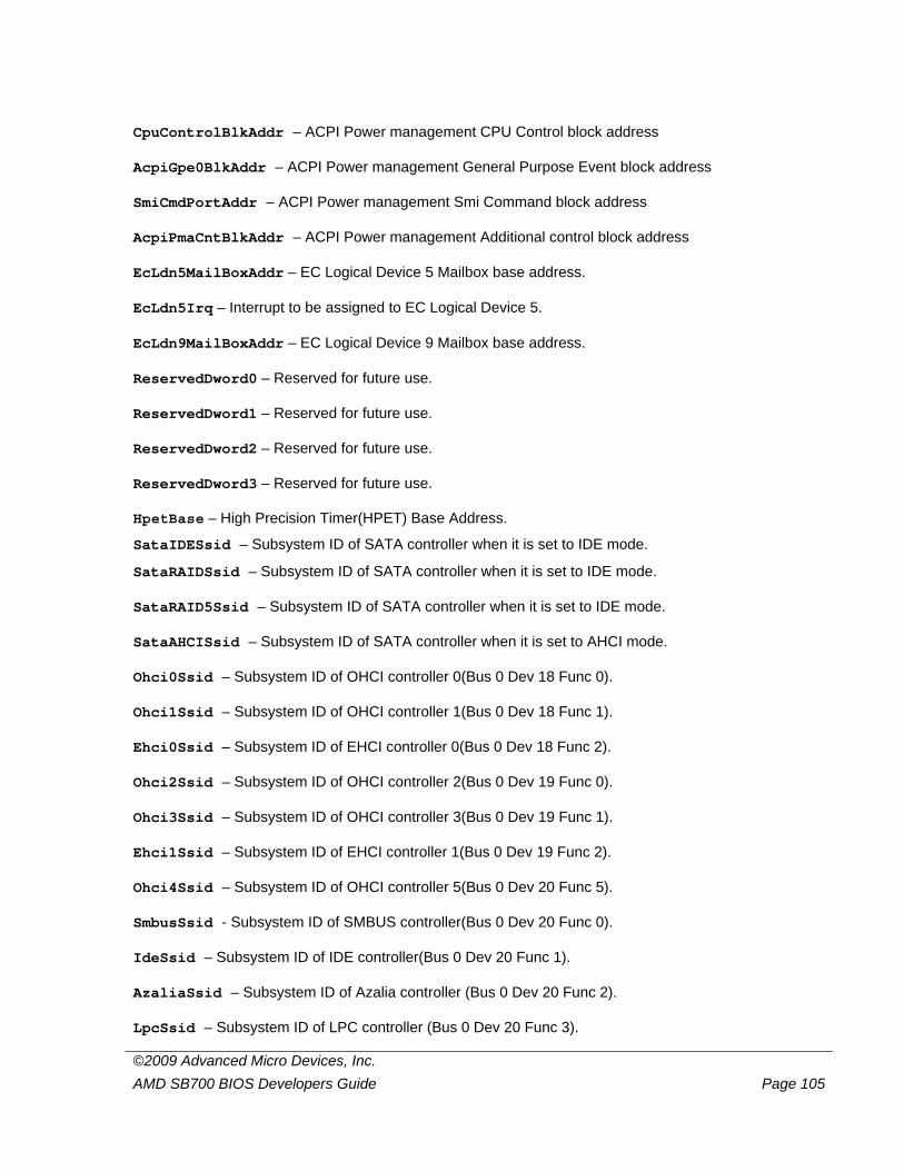
©2009 Advanced Micro Devices, Inc. AMD SB700 BIOS Developers Guide Page 105
CpuControlBlkAddr – ACPI Power management CPU Control block address AcpiGpe0BlkAddr – ACPI Power management General Purpose Event block address SmiCmdPortAddr – ACPI Power management Smi Command block address AcpiPmaCntBlkAddr – ACPI Power management Additional control block address EcLdn5MailBoxAddr – EC Logical Device 5 Mailbox base address. EcLdn5Irq – Interrupt to be assigned to EC Logical Device 5. EcLdn9MailBoxAddr – EC Logical Device 9 Mailbox base address. ReservedDword0 – Reserved for future use. ReservedDword1 – Reserved for future use. ReservedDword2 – Reserved for future use. ReservedDword3 – Reserved for future use. HpetBase – High Precision Timer(HPET) Base Address.
SataIDESsid – Subsystem ID of SATA controller when it is set to IDE mode.
SataRAIDSsid – Subsystem ID of SATA controller when it is set to IDE mode. SataRAID5Ssid – Subsystem ID of SATA controller when it is set to IDE mode. SataAHCISsid – Subsystem ID of SATA controller when it is set to AHCI mode. Ohci0Ssid – Subsystem ID of OHCI controller 0(Bus 0 Dev 18 Func 0). Ohci1Ssid – Subsystem ID of OHCI controller 1(Bus 0 Dev 18 Func 1). Ehci0Ssid – Subsystem ID of EHCI controller 0(Bus 0 Dev 18 Func 2). Ohci2Ssid – Subsystem ID of OHCI controller 2(Bus 0 Dev 19 Func 0). Ohci3Ssid – Subsystem ID of OHCI controller 3(Bus 0 Dev 19 Func 1). Ehci1Ssid – Subsystem ID of EHCI controller 1(Bus 0 Dev 19 Func 2). Ohci4Ssid – Subsystem ID of OHCI controller 5(Bus 0 Dev 20 Func 5). SmbusSsid - Subsystem ID of SMBUS controller(Bus 0 Dev 20 Func 0). IdeSsid – Subsystem ID of IDE controller(Bus 0 Dev 20 Func 1). AzaliaSsid – Subsystem ID of Azalia controller (Bus 0 Dev 20 Func 2). LpcSsid – Subsystem ID of LPC controller (Bus 0 Dev 20 Func 3).
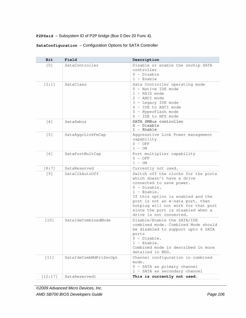
©2009 Advanced Micro Devices, Inc. AMD SB700 BIOS Developers Guide Page 106
P2PSsid – Subsystem ID of P2P bridge (Bus 0 Dev 20 Func 4).
SataConfiguration – Configuration Options for SATA Controller
Bit Field Description [0] SataController Disable or enable the onchip SATA
controller 0 – Disable 1 – Enable
[3:1] SataClass Sata Controller operating mode 0 – Native IDE mode 1 – RAID mode 2 – AHCI mode 3 – Legacy IDE mode 4 – IDE to AHCI mode 5 – HyperFlash mode 6 – IDE to HFS mode
[4] SataSmbus SATA SMBus controller 0 – Disable 1 - Enable
[5] SataAggrLinkPmCap Aggresstive Link Power management capability 0 – OFF 1 – ON
[6] SataPortMultCap Port multiplier capability 0 – OFF 1 - ON
[8:7] SataReserved Currently not used. [9] SataClkAutoOff Switch off the clocks for the ports
which doesn’t have a drive connected to save power. 0 – Disable. 1 – Enable. If this option is enabled and the port is not an e-sata port, then hotplug will not work for that port since the port is disabled when a drive is not connected.
[10] SataIdeCombinedMode Disable/Enable the SATA/IDE combined mode. Combined Mode should be disabled to support upto 6 SATA ports 0 – Disable. 1 – Enable. Combined mode is described in more detailed in BDG.
[11] SataIdeCombMdPriSecOpt Channel configuration in combined mode. 0 – SATA as primary channel 1 – SATA as secondary channel
[12:17] SataReserved1 This is currently not used.
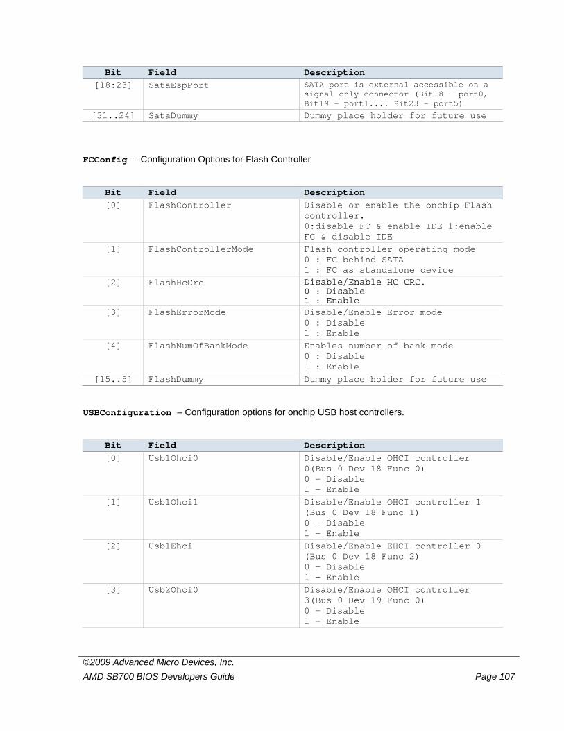
©2009 Advanced Micro Devices, Inc. AMD SB700 BIOS Developers Guide Page 107
Bit Field Description [18:23] SataEspPort SATA port is external accessible on a
signal only connector (Bit18 – port0, Bit19 – port1.... Bit23 – port5)
[31..24] SataDummy Dummy place holder for future use FCConfig – Configuration Options for Flash Controller
Bit Field Description [0] FlashController Disable or enable the onchip Flash
controller. 0:disable FC & enable IDE 1:enable FC & disable IDE
[1] FlashControllerMode Flash controller operating mode 0 : FC behind SATA 1 : FC as standalone device
[2] FlashHcCrc Disable/Enable HC CRC. 0 : Disable 1 : Enable
[3] FlashErrorMode Disable/Enable Error mode 0 : Disable 1 : Enable
[4] FlashNumOfBankMode Enables number of bank mode 0 : Disable 1 : Enable
[15..5] FlashDummy Dummy place holder for future use USBConfiguration – Configuration options for onchip USB host controllers.
Bit Field Description [0] Usb1Ohci0 Disable/Enable OHCI controller
0(Bus 0 Dev 18 Func 0) 0 – Disable 1 - Enable
[1] Usb1Ohci1 Disable/Enable OHCI controller 1 (Bus 0 Dev 18 Func 1) 0 – Disable 1 – Enable
[2] Usb1Ehci Disable/Enable EHCI controller 0 (Bus 0 Dev 18 Func 2) 0 – Disable 1 – Enable
[3] Usb2Ohci0 Disable/Enable OHCI controller 3(Bus 0 Dev 19 Func 0) 0 – Disable 1 – Enable
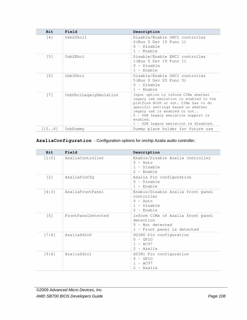
©2009 Advanced Micro Devices, Inc. AMD SB700 BIOS Developers Guide Page 108
Bit Field Description [4] Usb2Ohci1 Disable/Enable OHCI controller
4(Bus 0 Dev 19 Func 1) 0 – Disable 1 - Enable
[5] Usb2Ehci Disable/Enable EHCI controller 1(Bus 0 Dev 19 Func 1) 0 – Disable 1 – Enable
[6] Usb3Ohci Disable/Enable OHCI controller 5(Bus 0 Dev 20 Func 5) 0 – Disable 1 – Enable
[7] UsbOhciLegacyEmulation Input option to inform CIMx whether legacy usb emulation is enabled in the platform BIOS or not. CIMx has to do specific settings based on whether legacy usb is enabled or not.. 0 – USB Legacy emulation support is enabled. 1 – USB Legacy emulation is disabled.
[15..8] UsbDummy Dummy place holder for future use AzaliaConfiguration - Configuration options for onchip Azalia audio controller.
Bit Field Description [1:0] AzaliaController Enable/Disable Azalia controller
0 – Auto 1 – Disable 2 - Enable
[2] AzaliaPinCfg Azalia Pin configuration 0 – Disable 1 – Enable
[4:3] AzaliaFrontPanel Enable/Disable Azalia front panel controller 0 – Auto 1 – Disable 2 - Enable
[5] FrontPanelDetected Inform CIMx of Azalia front panel detection 0 – Not detected 1 – Front panel is detected
[7:6] AzaliaSdin0 SDIN0 Pin configuration 0 – GPIO 1 – AC97 2 - Azalia
[9:8] AzaliaSdin1 SDIN1 Pin configuration 0 – GPIO 1 – AC97 2 - Azalia
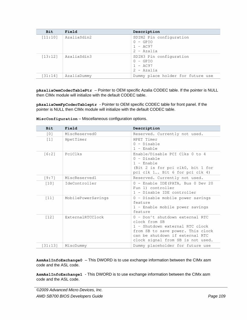
©2009 Advanced Micro Devices, Inc. AMD SB700 BIOS Developers Guide Page 109
Bit Field Description [11:10] AzaliaSdin2 SDIN2 Pin configuration
0 – GPIO 1 – AC97 2 - Azalia
[13:12] AzaliaSdin3 SDIN3 Pin configuration 0 – GPIO 1 – AC97 2 - Azalia
[31:14] AzaliaDummy Dummy place holder for future use pAzaliaOemCodecTablePtr – Pointer to OEM specific Azalia CODEC table. If the pointer is NULL then CIMx module will initialize with the default CODEC table. pAzaliaOemFpCodecTableptr - Pointer to OEM specific CODEC table for front panel. If the pointer is NULL then CIMx module will initialize with the default CODEC table. MiscConfiguration – Miscellaneous configuration options.
Bit Field Description [0] MiscReserved0 Reserved. Currently not used. [1] HpetTimer HPET Timer
0 – Disable 1 – Enable
[6:2] PciClks Enable/Disable PCI Clks 0 to 4 0 – Disable 1 – Enable (Bit 2 is for pci clk0, bit 1 for pci clk 1…. Bit 6 for pci clk 4)
[9:7] MiscReserved1 Reserved. Currently not used. [10] IdeController 0 – Enable IDE(PATA, Bus 0 Dev 20
Fun 1) controller 1 – Disable IDE controller
[11] MobilePowerSavings 0 – Disable mobile power savings feature 1 – Enable mobile power savings feature
[12] ExternalRTCClock 0 – Don’t shutdown external RTC clock from SB 1 – Shutdown external RTC clock from SB to save power. This clock can be shutdown if external RTC clock signal from SB is not used.
[31:13] MiscDummy Dummy placeholder for future use AsmAslInfoExchange0 – This DWORD is to use exchange information between the CIMx asm code and the ASL code. AsmAslInfoExchange1 - This DWORD is to use exchange information between the CIMx asm code and the ASL code.
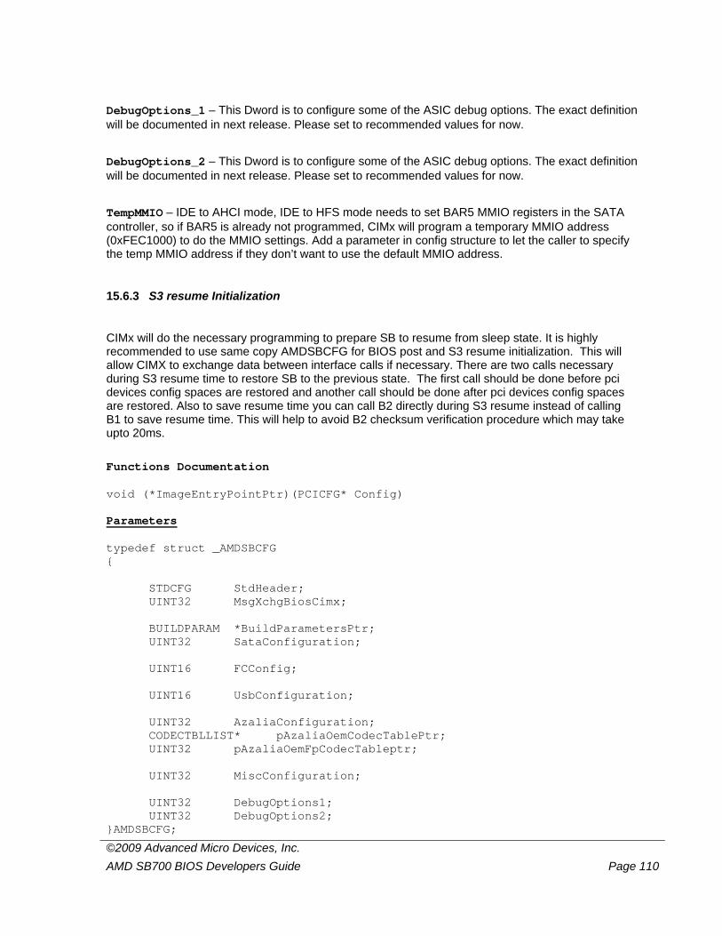
©2009 Advanced Micro Devices, Inc. AMD SB700 BIOS Developers Guide Page 110
DebugOptions_1 – This Dword is to configure some of the ASIC debug options. The exact definition will be documented in next release. Please set to recommended values for now.
DebugOptions_2 – This Dword is to configure some of the ASIC debug options. The exact definition will be documented in next release. Please set to recommended values for now.
TempMMIO – IDE to AHCI mode, IDE to HFS mode needs to set BAR5 MMIO registers in the SATA controller, so if BAR5 is already not programmed, CIMx will program a temporary MMIO address (0xFEC1000) to do the MMIO settings. Add a parameter in config structure to let the caller to specify the temp MMIO address if they don’t want to use the default MMIO address.
15.6.3 S3 resume Initialization
CIMx will do the necessary programming to prepare SB to resume from sleep state. It is highly recommended to use same copy AMDSBCFG for BIOS post and S3 resume initialization. This will allow CIMX to exchange data between interface calls if necessary. There are two calls necessary during S3 resume time to restore SB to the previous state. The first call should be done before pci devices config spaces are restored and another call should be done after pci devices config spaces are restored. Also to save resume time you can call B2 directly during S3 resume instead of calling B1 to save resume time. This will help to avoid B2 checksum verification procedure which may take upto 20ms.
Functions Documentation void (*ImageEntryPointPtr)(PCICFG* Config)
Parameters typedef struct _AMDSBCFG { STDCFG StdHeader; UINT32 MsgXchgBiosCimx; BUILDPARAM *BuildParametersPtr; UINT32 SataConfiguration; UINT16 FCConfig; UINT16 UsbConfiguration; UINT32 AzaliaConfiguration; CODECTBLLIST* pAzaliaOemCodecTablePtr; UINT32 pAzaliaOemFpCodecTableptr; UINT32 MiscConfiguration; UINT32 DebugOptions1; UINT32 DebugOptions2; }AMDSBCFG;
©2009 Advanced Micro Devices, Inc. AMD SB700 BIOS Developers Guide Page 111
Detail Description stdHeader – Standard function call (see STDCFG definition).
stdHeader.Func = 0x40 – Before pci restoration stdHeader.Func = 0x50 – After pci restoration
15.7 Callback Interface Definition
Callback functions are supported in CIMx module to enable the OEMs to hook at a specific place in the CIMx module. This will enable the OEMs to do some specific initialization inbetween the CIMx functions. OEMs who require some callbacks can request AMD to add this call in CIMx.
15.7.1 SATA OEM Call Back “SATA_PHY_PROGRAMMING”
This callback function is dedicated to program the SATA PHY settings specific to the platform. Functions Documentation: UINT32 (*pCallBack)(UINTN Param1, UINTN Param2, PCICFG* pConfig) Parameters: Param1: Function identifier (OEM_CALLBACK_BASE + 0x10, defaults to 0x110) Param2: NULL. pConfig: See SB Config Structure Definition in (section 1.6.2) Return Values: CIM_SUCCESS (0x00000000): If platform has implemented this callback function and programmed the PHY values according to platform. CIM_UNSUPPORTED (0x80000001): If platform does not have this callback function implemented.
15.7.2 Integrated Pull-up and Pull-down Settings “PULL_UP_PULL_DOWN_SETTINGS”
This callback function is dedicated to program the integrated pull-up and pull-down settings specific to the platform. The BIOS needs to set pull-up/down settings for GEVENT/GPM platform specifically. These pins have integrated pull-up/down enabled by default and they are powered by the S5 power. If they are to be connected to a device that will be powered down during sleep state, the BIOS should disable the pull-up/down and use external pull-up/down to avoid leakage. Functions Documentation: UINT32 (*pCallBack) (UINTN Param1, UINTN Param2, PCICFG* pConfig) Parameters: Param1: Function identifier (OEM_CALLBACK_BASE + 0x20, defaults to 0x120) Param2: NULL. pConfig: See SB Config Structure Definition in (section 1.6.2) Return Values: CIM_SUCCESS (0x00000000): If platform has implemented this callback function and programmed the integrated pull-up & pull-down settings according to platform. CIM_UNSUPPORTED (0x80000001): If platform does not have this callback function implemented.
©2009 Advanced Micro Devices, Inc. AMD SB700 BIOS Developers Guide Page 112
15.8 SMM Functions Support
Currently SMM functions are not supported in the SB700 CIMx module.
15.9 Reference Code
The reference code is in the refcode directory of the CIMx module. Following is a short description of the files with the definitions and the codes contained in them. PUSHHIGH.INC – Header file which defines the equates used by bridge files BRIDGE32.INC – Sample code to switch from Real mode to Protected and then call the CIMx and then switch back to real mode. BRIDGE32X.INC – Sample code to enable the caching (WriteThrough) for the CIMx module. AMDSBCFG.INC – Sample definition of config struction and equates used in the SB700 CIMx module. AMDSBBB.ASM – Sample implementation of the CIMx wrapper before memory is available (for sbPowerOnInit call). AMDSB.ASM – Sample implementation of the CIMx wrapper after memory is available. HWM.INC – Sample code for the hardware monitor initialization feature of SB700.
©2009 Advanced Micro Devices, Inc. AMD SB700 BIOS Developers Guide Page 113
Appendix: Revision History
Date Rev. PDF Description
June, 2009 1.00 43366_sb7xx_bdg_pub_1.00 First public release.
Based on NDA release rev 1.02.