Embed Size (px)
Citation preview
This is information on a product in full production. For further information contact your local STMicroelectronics sales office.
July 2012 Doc ID 023407 Rev 1 1/24
24
STA662
AM/FM, DAB/DAB+/DMB-A, DRM multi-standard digital radio receiver
Data brief − production data
Features■ General
– Multi-standard digital radio channel decoding– Multi-standard digital radio source
decoding (MPEG-1 AL II, AAC+, BSAC)– AM/FM phase diversity– Multiple streams parallel processing FM
phase diversity plus two DAB channels– Audio processing– Audio streaming from SD Card, CD ROM
(optional)
■ Supported radio systems– AM, FM including phase diversity– DAB, DAB+, DMB-Audio, DRM– HD Radio™ (interface to co-processor
STA680)
■ Hardware– ARM946™ core running at 131.328 MHz– STxP70 DSP core running at 262.256 or
131.328 MHz– Emerald DSP core running at 131.328 MHz– Multilayer AMBA architecture (6 AHB + 3 APB)– DMA supporting 16 channels on 4
dedicated AHB layers– VIC supporting vectored and standard
interrupt requests– Hardware support for conditional access
(one-time programmable 768-bit memory)– 2 internal PLLs:
System PLL for cores and peripherals Fractional PLL for audio clocks input
■ Memories– 64 KB Internal ROM– 740 KB of Internal RAM available for cores – 512 KB configurable DAB de-interleaving
memory– SPI Flash interface for application code
loading running up to 16 MHz (optional SD/MMC)
– External SDR-SDRAM interface: 2 x 512 Mbit, 16-bit data bus
■ Turner interface– 4 RF Front End LVDS interface– 4 master SPI interface for tuners control
■ Other interfaces– Audio interfaces (up to 8 independent and
configurable I2S based on 45.6 kHz rate)– Enhanced audio interface (fully
configurable I2S) – 2 S/PDIF receiver– I2C interface– 3 UART - GPIO interface (24 dedicated lines)– Micro IF (based on 2 RX SPI + 2 TX SPI
slave only + 4 audio clocks)– 5 timers– JTAG and ETM interfaces
■ Power supplies– Core supply: 1.2 V– I/O supply: 3.3 V– Triple voltage I/O supply for host processor
interface: 1.8 V / 2.5 V / 3.3 V– Analog supply: 2.5 V (external or internal LDO)
■ Applications– Multi-standard smart tuner module– Multi-standard car-radio receiver– Home receivers
Table 1. Device summary
Order code Temp range Package Packing
STA662 -40 °C to +85 °C TFBGA289 Tray
TFBGA289
www.st.com
Contents STA662
2/24 Doc ID 023407 Rev 1
Contents
1 Description . . . . . . . . . . . . . . . . . . . . . . . . . . . . . . . . . . . . . . . . . . . . . . . . . 3
1.1 DAB signal processing . . . . . . . . . . . . . . . . . . . . . . . . . . . . . . . . . . . . . . . . 4
1.2 FM signal processing . . . . . . . . . . . . . . . . . . . . . . . . . . . . . . . . . . . . . . . . . 5
1.3 AM signal processing . . . . . . . . . . . . . . . . . . . . . . . . . . . . . . . . . . . . . . . . . 6
1.4 Multiple DAB radio stream parallel processing . . . . . . . . . . . . . . . . . . . . . . 6
1.5 Overview of main functional blocks . . . . . . . . . . . . . . . . . . . . . . . . . . . . . . 7
1.5.1 STA662 architecture . . . . . . . . . . . . . . . . . . . . . . . . . . . . . . . . . . . . . . . . 7
1.5.2 ARM946 subsystem . . . . . . . . . . . . . . . . . . . . . . . . . . . . . . . . . . . . . . . . . 8
1.5.3 DSP-STxP70 subsystem . . . . . . . . . . . . . . . . . . . . . . . . . . . . . . . . . . . . . 8
1.5.4 DSP-Emerald subsystem . . . . . . . . . . . . . . . . . . . . . . . . . . . . . . . . . . . . . 8
1.5.5 IPBUS subsytem . . . . . . . . . . . . . . . . . . . . . . . . . . . . . . . . . . . . . . . . . . . 9
1.5.6 Embedded memories . . . . . . . . . . . . . . . . . . . . . . . . . . . . . . . . . . . . . . . . 9
1.5.7 SDR-SDRAM controller . . . . . . . . . . . . . . . . . . . . . . . . . . . . . . . . . . . . . . 9
1.5.8 Hardware accelerators . . . . . . . . . . . . . . . . . . . . . . . . . . . . . . . . . . . . . . 10
1.5.9 Audio interface . . . . . . . . . . . . . . . . . . . . . . . . . . . . . . . . . . . . . . . . . . . . 10
1.5.10 Enhanced serial audio interface . . . . . . . . . . . . . . . . . . . . . . . . . . . . . . 10
1.5.11 Serial link and front end interface . . . . . . . . . . . . . . . . . . . . . . . . . . . . . 11
1.5.12 APB peripherals . . . . . . . . . . . . . . . . . . . . . . . . . . . . . . . . . . . . . . . . . . . 11
1.5.13 System management unit . . . . . . . . . . . . . . . . . . . . . . . . . . . . . . . . . . . 11
1.5.14 Clock and reset distribution unit . . . . . . . . . . . . . . . . . . . . . . . . . . . . . . . 11
2 Pin description . . . . . . . . . . . . . . . . . . . . . . . . . . . . . . . . . . . . . . . . . . . . 12
2.1 Ball out . . . . . . . . . . . . . . . . . . . . . . . . . . . . . . . . . . . . . . . . . . . . . . . . . . . 12
2.2 STA662 pin list . . . . . . . . . . . . . . . . . . . . . . . . . . . . . . . . . . . . . . . . . . . . . 13
2.3 Pins termination . . . . . . . . . . . . . . . . . . . . . . . . . . . . . . . . . . . . . . . . . . . . 21
3 Package information . . . . . . . . . . . . . . . . . . . . . . . . . . . . . . . . . . . . . . . . 22
4 Revision history . . . . . . . . . . . . . . . . . . . . . . . . . . . . . . . . . . . . . . . . . . . 23
STA662 Description
Doc ID 023407 Rev 1 3/24
1 Description
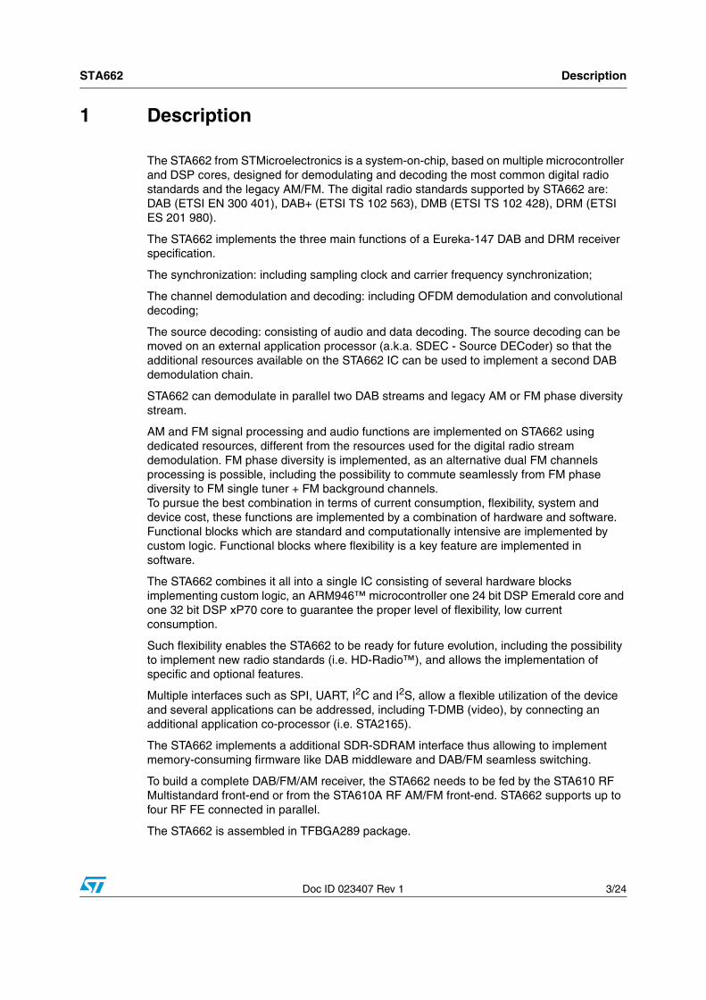
The STA662 from STMicroelectronics is a system-on-chip, based on multiple microcontroller and DSP cores, designed for demodulating and decoding the most common digital radio standards and the legacy AM/FM. The digital radio standards supported by STA662 are: DAB (ETSI EN 300 401), DAB+ (ETSI TS 102 563), DMB (ETSI TS 102 428), DRM (ETSI ES 201 980).
The STA662 implements the three main functions of a Eureka-147 DAB and DRM receiver specification.
The synchronization: including sampling clock and carrier frequency synchronization;
The channel demodulation and decoding: including OFDM demodulation and convolutional decoding;
The source decoding: consisting of audio and data decoding. The source decoding can be moved on an external application processor (a.k.a. SDEC - Source DECoder) so that the additional resources available on the STA662 IC can be used to implement a second DAB demodulation chain.
STA662 can demodulate in parallel two DAB streams and legacy AM or FM phase diversity stream.
AM and FM signal processing and audio functions are implemented on STA662 using dedicated resources, different from the resources used for the digital radio stream demodulation. FM phase diversity is implemented, as an alternative dual FM channels processing is possible, including the possibility to commute seamlessly from FM phase diversity to FM single tuner + FM background channels.To pursue the best combination in terms of current consumption, flexibility, system and device cost, these functions are implemented by a combination of hardware and software. Functional blocks which are standard and computationally intensive are implemented by custom logic. Functional blocks where flexibility is a key feature are implemented in software.
The STA662 combines it all into a single IC consisting of several hardware blocks implementing custom logic, an ARM946™ microcontroller one 24 bit DSP Emerald core and one 32 bit DSP xP70 core to guarantee the proper level of flexibility, low current consumption.
Such flexibility enables the STA662 to be ready for future evolution, including the possibility to implement new radio standards (i.e. HD-Radio™), and allows the implementation of specific and optional features.
Multiple interfaces such as SPI, UART, I2C and I2S, allow a flexible utilization of the device and several applications can be addressed, including T-DMB (video), by connecting an additional application co-processor (i.e. STA2165).
The STA662 implements a additional SDR-SDRAM interface thus allowing to implement memory-consuming firmware like DAB middleware and DAB/FM seamless switching.
To build a complete DAB/FM/AM receiver, the STA662 needs to be fed by the STA610 RF Multistandard front-end or from the STA610A RF AM/FM front-end. STA662 supports up to four RF FE connected in parallel.
The STA662 is assembled in TFBGA289 package.
Description STA662
4/24 Doc ID 023407 Rev 1
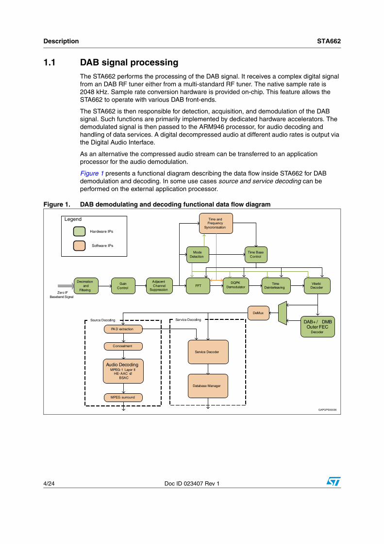
1.1 DAB signal processingThe STA662 performs the processing of the DAB signal. It receives a complex digital signal from an DAB RF tuner either from a multi-standard RF tuner. The native sample rate is 2048 kHz. Sample rate conversion hardware is provided on-chip. This feature allows the STA662 to operate with various DAB front-ends.
The STA662 is then responsible for detection, acquisition, and demodulation of the DAB signal. Such functions are primarily implemented by dedicated hardware accelerators. The demodulated signal is then passed to the ARM946 processor, for audio decoding and handling of data services. A digital decompressed audio at different audio rates is output via the Digital Audio Interface.
As an alternative the compressed audio stream can be transferred to an application processor for the audio demodulation.
Figure 1 presents a functional diagram describing the data flow inside STA662 for DAB demodulation and decoding. In some use cases source and service decoding can be performed on the external application processor.
Figure 1. DAB demodulating and decoding functional data flow diagram
STA662 Description
Doc ID 023407 Rev 1 5/24
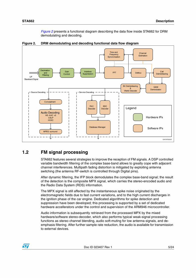
Figure 2 presents a functional diagram describing the data flow inside STA662 for DRM demodulating and decoding.
Figure 2. DRM demodulating and decoding functional data flow diagram
1.2 FM signal processingSTA662 features several strategies to improve the reception of FM signals. A DSP controlled variable bandwidth filtering of the complex base-band allows to greatly cope with adjacent channel interferences. Multipath fading distortion is mitigated by exploiting antenna switching (the antenna RF-switch is controlled through Digital pins).
After dynamic filtering, the IFP block demodulates the complex base-band signal; the result of the detection is the composite MPX signal, which carries the stereo-encoded audio and the Radio Data System (RDS) information.
The MPX signal is still affected by the instantaneous spike noise originated by the electromagnetic fields due to fast current variations, and to the high current discharges in the ignition phase of the car engine. Dedicated algorithms for spike detection and suppression have been developed; this processing is supported by a set of dedicated hardware accellerators under the control and supervision of the ARM946 microcontroller.
Audio information is subsequently retrieved from the processed MPX by the mixed hardware/software stereo-decoder, which also performs typical weak-signal processing functions as stereo channel blending, audio soft-muting for low antenna signals, and de-emphasis filtering. After further sample rate reduction, the audio is available for transmission to external devices.
Description STA662
6/24 Doc ID 023407 Rev 1
1.3 AM signal processingAM bandwidth is about one-twentieth of the FM, thus additional filtering and decimation is required after the DDC. The hardware demodulator in the IFP block is used for evaluating the amplitude of the complex base-band. Similarly to FM signals, engine-injection-related spikes are a concern; spike detection and noise-blanking are performed on the audio signal, on the contrary since multipath distortion is not a major issue in AM, no antenna switching is necessary.
1.4 Multiple DAB radio stream parallel processingSTA662 is capable to simultaneously demodulate two different DAB Radio streams. This unique feature enables the device to decode a DAB Radio audio stream, in parallel with any data service broadcasted by a different radio channel. The implementation of the dual streams DAB Radio processing requires that two DAB or Multi-standard RF tuners are connected to the STA662.
In a single channel implementation a single RF tuner is used. In such configuration STA662 is able to demodulate at the same time both the audio and the data carried inside a single DAB ensemble. This means that the user can listen audio and receive traffic information or data broadcasted on that specific single ensemble.
In a dual DAB channels implementation STA662 can simultaneously demodulate audio and data associated to different ensembles. This means that in the example above it would be still possible to receive traffic information broadcasted on ensemble A while listening audio program broadcasted on ensemble B.
STA662 can always perform FM phase diversity reception in parallel with DAB channels decoding.
The audio coming from any AM/FM/DAB/DRM channel is output in I2S digital format. The I2S configurable protocol is well-suited for sending data to external audio processors or digital-in power amplifier.
STA662 Description
Doc ID 023407 Rev 1 7/24
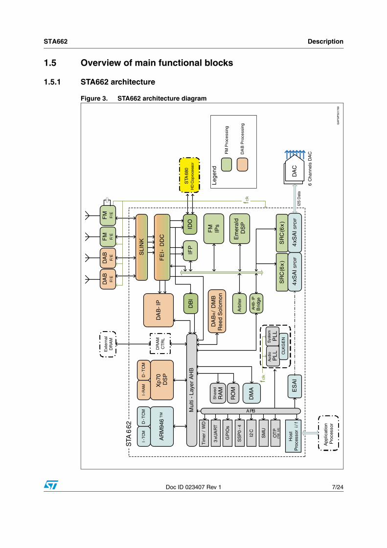
1.5 Overview of main functional blocks
1.5.1 STA662 architecture
Figure 3. STA662 architecture diagram
Description STA662
8/24 Doc ID 023407 Rev 1
1.5.2 ARM946 subsystem
A 32-bit ARM946 microcontroller with ITCM and DTCM is embedded into STA662. It controls the I/O peripherals, the hardware accelerator modules, the DSP-Emerald subsystem and the DSP STxP70 subsystem.
The ARM946 is used for:
● System and data flow control
● Peripherals initialisation
● RDS alternate frequency switching strategy
and in some application can be also used for:
● DAB/DAB+ database management
● Seamless linking
The STA662 embeds into the ARM946 subsystem both program and data cache to improve performance during code execution. Also, the amount of Tightly Coupled Memory (TCM) assigned to the core can be defined by the user at start-up.
The ARM946 uses a trace macro-cell (ETM9) with a trace debug port (JTAG) for in-system programming and debugging tools. JTAG is also shared with the DSP-Emerald subsystem and STxp70 subsystem.
An AHB bus matrix is implemented for connecting the 6 AHB masters (ARM, xp70 and 4 DMAs) with all the AHB slaves.
Flexible DMA resources are available for data movement while VIC logic is implemented to managed interrupt requests.
1.5.3 DSP-STxP70 subsystem
STA662 includes a 32-bit STxP70- with DTCM and L2Pram. MPx and FPx extensions are connected to the core.
The STxP70 is used for:
● DRM channel decoding
● DAB channel time and frequency synchronization
● Audio decoding
The STxP70 subsystem contains a program cache to improve performance during code execution. AHB master port is used by the DSP to access the STA662 architecture while an AHB slave port is used by DMA to access xp70 subsystem memories.
Debugging of the software running on the DSP-STxp70 is possible through the JTAG interface.
1.5.4 DSP-Emerald subsystem
STA662 includes a 24-bit DSP-Emerald core connected to the hardware-accelerator (HAR) modules and to the microcontroller via the IPBUS.
The Emerald core is used for:
● FM processing
● AM processing
● Audio processing
STA662 Description
Doc ID 023407 Rev 1 9/24
The Emerald DSP is connected to the AHB bus matrix through an AHB slave port.
Debugging of the software running on the DSP-Emerald is possible through the JTAG interface.
1.5.5 IPBUS subsytem
The IPBUS is a multi-master bus, connecting hardware accelerators for AM/FM and Audio processing, the DSP-Emerald subsystem and the AMBA subsystem. Access to the IPBUS is controlled by a dedicated arbiter module (ARB).
Potential bus masters are:
● The BCO (Bus COntrol) unit is used for managing the IPBUS transfers. This unit provides one set of programmable (synchronous or isochronous) transfers
● The ARM946 which is intended as STA662 system controller
● The DMA channels for data exchange
● The STxp70 for specific data processing
● The SPI debug interface for debugging and monitoring the subsystem
The IPBUS subsystem is connected to the AHB bus matrix through the AHB2IPBUS Bridge.
1.5.6 Embedded memories
STA662 offers a flexible solution for allocating memories to the cores or IPs.
Default configuration is:
● 8KB+128KB of D and I TCMs and 8KB+16KB of D & P caches for the ARM core
● 160KB of DTCM, 8KB Pcache and 64KB L2 program memory for the STxP70 DSP
● 18 KB+18KB X & Y RAM, 24 KB PRAM and 64 KB PROM for the Emerald core
● 64 KB of AHB ROM and 256 KB of AHB RAM
● 2 x 256KB of de-interleaving memory for the DAB-IP
AHB memories are available for both the AHB mapped cores: ARM946 and STxP70.
DAB-IP de-interleaving memory if not used for the DAB channel decoding can be remapped as ARM TCM or AHB memory.
Part of the AHB memory can be remapped as ARM946 TCM.
STxP70 L2 memory and D-TCM are mapped on the AHB and then available for the AHB masters.
Emerald memories are mapped on the AHB and available for the AHB masters.
1.5.7 SDR-SDRAM controller
STA662 embeds an SDR-SDRAM controller. The controller is connected to the AHB multi layer architecture so that it expands the memory available for both the AHB mapped cores: ARM946 and STxP70.
SDRAM controller clock is selectable by a top level register between four different possibilities: full rate, which corresponds to the ARM9 core frequency (131.328 MHz), or this frequency divided by a factor 2, 4 or 8.
Description STA662
10/24 Doc ID 023407 Rev 1
1.5.8 Hardware accelerators
STA662 uses an optimized partitioning of the processing functions among Emerald, ARM946, STxP70 and special-purpose hardware resources. Thanks to this strategy, high CPU-intensive routines take advantage of dedicated hardware processing blocks, though ensuring flexibility and customizability provided by the Emerald and STxP70 DSPs and the ARM946 embedded microcontroller; in fact, ARM946 is monitoring and controlling the processing running both on Emerald, STxP70 and on the dedicated peripherals.
The list of hardware accelerators embedded into the STA662 comprises:
● DAB demodulator compliant with the EUREKA 147 standard for Digital Audio Broadcasting
● RS-DEC DMB
● RS-DEC DAB+
● FM/AM Digital Intelligent Selectivity System (D-ISS)
● FM/AM Stereo matrix separation
● FM/AM Virtual Phase-array Antenna switching strategy
● FM/AM Antenna Switching Diversity control (ASD)
● FM/AM RDS demodulation and decoding (RDS)
● Audio processing programmable filters
1.5.9 Audio interface
The Audio Interface (AIF) is used to exchange digital audio data with external devices using different Serial Audio Interface (SAI1-4) or S/PDIF protocols into the IPBUS subsystem.
Two AIF modules have been integrated into STA662.
The 6-channels Stereo Low Pass Filter (LPF6CH) can be used to apply programmable low pass filtering to the audio signal.
The 6-channels Stereo Channel Sample Rate Converter (SRC6) introduces flexibility to the system, since it allows exchanging data with external units whose data rate is different from the STA662 one.
Signal routing to and from the STA662 is ruled by the internal audio Input/Output multiplexer (AIMUX/AOMUX) configurable by software.
1.5.10 Enhanced serial audio interface
The Enhanced Serial Audio Interface (ESAI) is a serial synchronous interface intended to give transfer capability of digital audio samples or more generally digital data between the AMBA architecture and external devices.
A clock divider logic gives the flexibility to the macro to generate all the needed audio clock rates. Master TX and slave RX are supported.TX and RX FIFO are available to reduce the load of the data channels inside the AMBA architecture.
STA662 Description
Doc ID 023407 Rev 1 11/24
1.5.11 Serial link and front end interface
The Serial Link (SLINK) and the Front End interface (FEI) blocks have been designed to connect the STA662 with different kind of tuners such as STA606 or STA610. The SLINK block performs serial to parallel conversion of data coming from the tuners while the FEI block performs decimation, filtering and other digital signal processing such as gain control, DC offset cancellation, image rejection and so on.
The Frontend interface is made up of four processing path: two dedicated to DAB and two to AM, FM, HD Radio or DRM baseband signal processing. If the system clock is provided by a frontend tuner then this FE must be connected to interface number 2 or 3.
1.5.12 APB peripherals
Three dedicated peripheral bus (APB0, APB1 and APBC) connect the AMBA architecture to several interfaces like 5 x SSP, EFT, MTU, I2C, GPIO, 3 x UART and Host interfaces.
1.5.13 System management unit
A system management unit (SMU) has been designed to control all the top level functionalities. These register are mapped on the APBC bus.
1.5.14 Clock and reset distribution unit
A clock and reset distribution unit (CRDU) is designed to generate and distribute all the needed clocks and resets. A System PLL and an Audio PLL are part of this logic.
Pin description STA662
12/24 Doc ID 023407 Rev 1
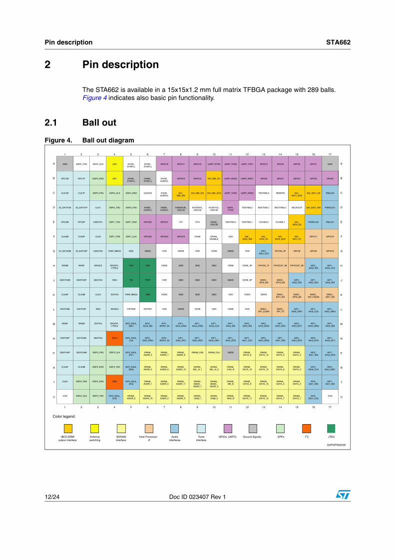
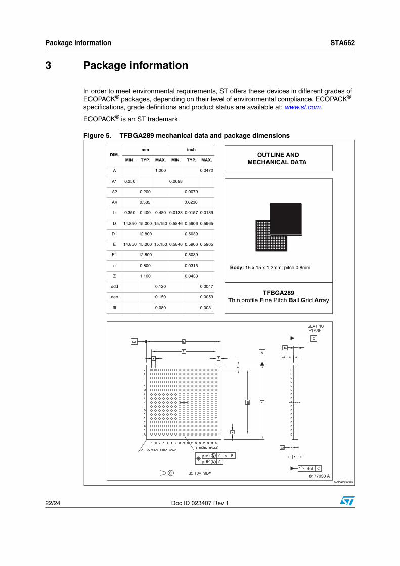
2 Pin description
The STA662 is available in a 15x15x1.2 mm full matrix TFBGA package with 289 balls. Figure 4 indicates also basic pin functionality.
2.1 Ball out
Figure 4. Ball out diagram
STA662 Pin description
Doc ID 023407 Rev 1 13/24
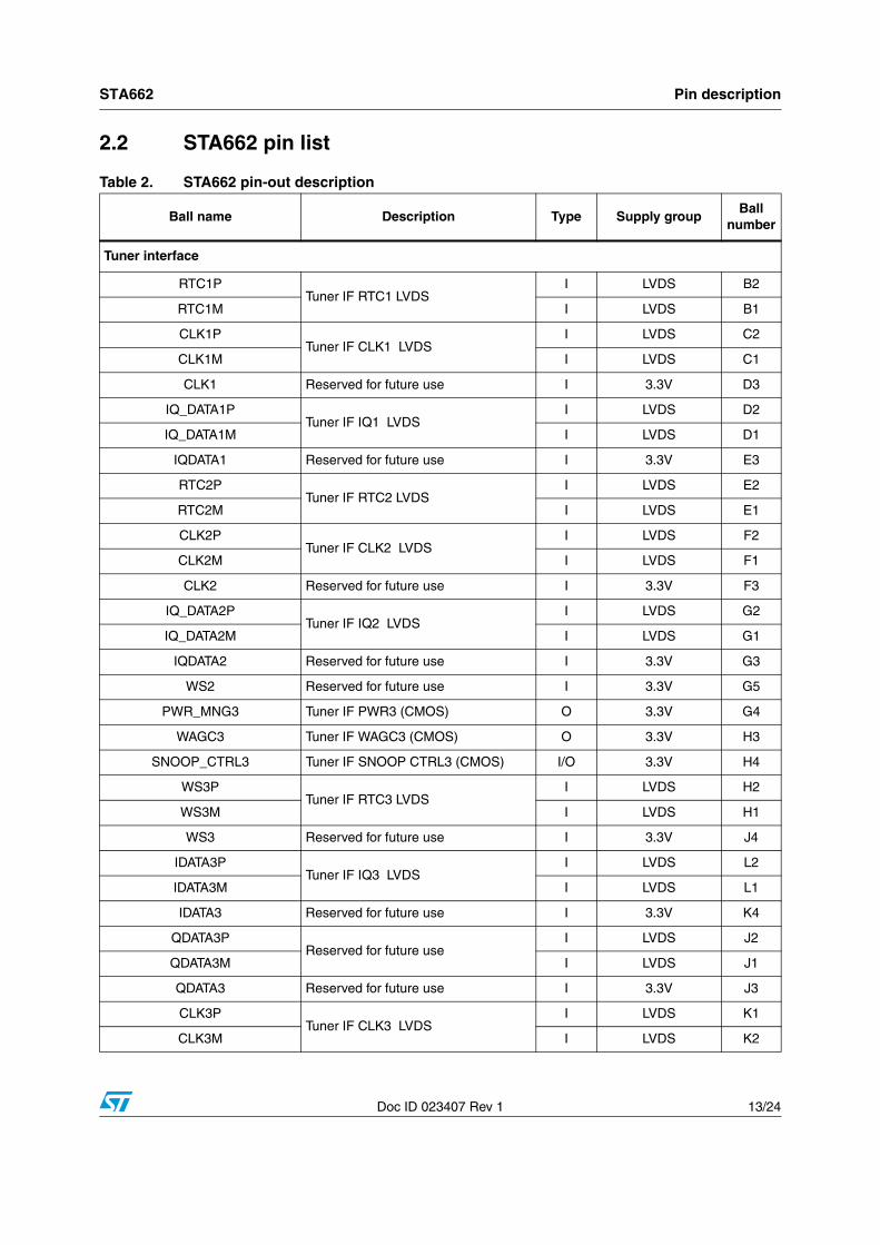
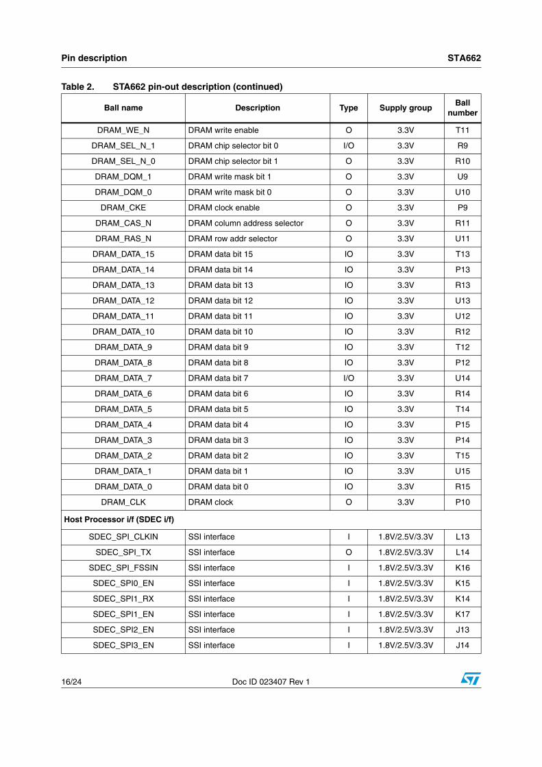
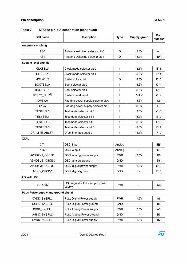
2.2 STA662 pin list
Table 2. STA662 pin-out description
Ball name Description Type Supply groupBall
number
Tuner interface
RTC1PTuner IF RTC1 LVDS
I LVDS B2
RTC1M I LVDS B1
CLK1PTuner IF CLK1 LVDS
I LVDS C2
CLK1M I LVDS C1
CLK1 Reserved for future use I 3.3V D3
IQ_DATA1PTuner IF IQ1 LVDS
I LVDS D2
IQ_DATA1M I LVDS D1
IQDATA1 Reserved for future use I 3.3V E3
RTC2PTuner IF RTC2 LVDS
I LVDS E2
RTC2M I LVDS E1
CLK2PTuner IF CLK2 LVDS
I LVDS F2
CLK2M I LVDS F1
CLK2 Reserved for future use I 3.3V F3
IQ_DATA2PTuner IF IQ2 LVDS
I LVDS G2
IQ_DATA2M I LVDS G1
IQDATA2 Reserved for future use I 3.3V G3
WS2 Reserved for future use I 3.3V G5
PWR_MNG3 Tuner IF PWR3 (CMOS) O 3.3V G4
WAGC3 Tuner IF WAGC3 (CMOS) O 3.3V H3
SNOOP_CTRL3 Tuner IF SNOOP CTRL3 (CMOS) I/O 3.3V H4
WS3PTuner IF RTC3 LVDS
I LVDS H2
WS3M I LVDS H1
WS3 Reserved for future use I 3.3V J4
IDATA3PTuner IF IQ3 LVDS
I LVDS L2
IDATA3M I LVDS L1
IDATA3 Reserved for future use I 3.3V K4
QDATA3PReserved for future use
I LVDS J2
QDATA3M I LVDS J1
QDATA3 Reserved for future use I 3.3V J3
CLK3PTuner IF CLK3 LVDS
I LVDS K1
CLK3M I LVDS K2
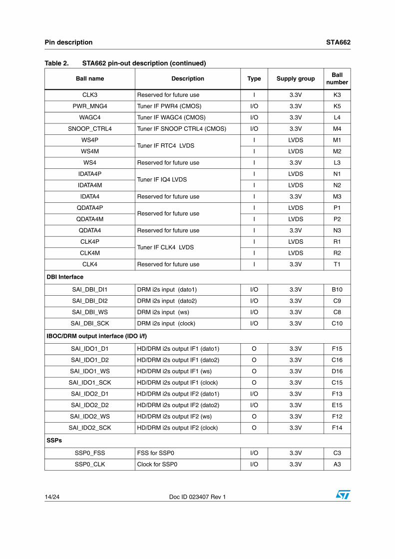
Pin description STA662
14/24 Doc ID 023407 Rev 1
CLK3 Reserved for future use I 3.3V K3
PWR_MNG4 Tuner IF PWR4 (CMOS) I/O 3.3V K5
WAGC4 Tuner IF WAGC4 (CMOS) I/O 3.3V L4
SNOOP_CTRL4 Tuner IF SNOOP CTRL4 (CMOS) I/O 3.3V M4
WS4PTuner IF RTC4 LVDS
I LVDS M1
WS4M I LVDS M2
WS4 Reserved for future use I 3.3V L3
IDATA4PTuner IF IQ4 LVDS
I LVDS N1
IDATA4M I LVDS N2
IDATA4 Reserved for future use I 3.3V M3
QDATA4PReserved for future use
I LVDS P1
QDATA4M I LVDS P2
QDATA4 Reserved for future use I 3.3V N3
CLK4PTuner IF CLK4 LVDS
I LVDS R1
CLK4M I LVDS R2
CLK4 Reserved for future use I 3.3V T1
DBI Interface
SAI_DBI_DI1 DRM i2s input (dato1) I/O 3.3V B10
SAI_DBI_DI2 DRM i2s input (dato2) I/O 3.3V C9
SAI_DBI_WS DRM i2s input (ws) I/O 3.3V C8
SAI_DBI_SCK DRM i2s input (clock) I/O 3.3V C10
IBOC/DRM output interface (IDO i/f)
SAI_IDO1_D1 HD/DRM i2s output IF1 (dato1) O 3.3V F15
SAI_IDO1_D2 HD/DRM i2s output IF1 (dato2) O 3.3V C16
SAI_IDO1_WS HD/DRM i2s output IF1 (ws) O 3.3V D16
SAI_IDO1_SCK HD/DRM i2s output IF1 (clock) O 3.3V C15
SAI_IDO2_D1 HD/DRM i2s output IF2 (dato1) I/O 3.3V F13
SAI_IDO2_D2 HD/DRM i2s output IF2 (dato2) I/O 3.3V E15
SAI_IDO2_WS HD/DRM i2s output IF2 (ws) O 3.3V F12
SAI_IDO2_SCK HD/DRM i2s output IF2 (clock) O 3.3V F14
SSPs
SSP0_FSS FSS for SSP0 I/O 3.3V C3
SSP0_CLK Clock for SSP0 I/O 3.3V A3
Table 2. STA662 pin-out description (continued)
Ball name Description Type Supply groupBall
number
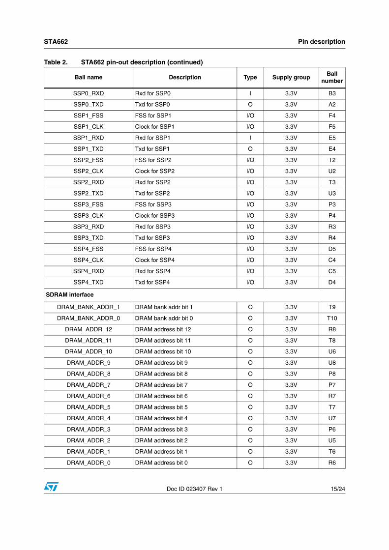
STA662 Pin description
Doc ID 023407 Rev 1 15/24
SSP0_RXD Rxd for SSP0 I 3.3V B3
SSP0_TXD Txd for SSP0 O 3.3V A2
SSP1_FSS FSS for SSP1 I/O 3.3V F4
SSP1_CLK Clock for SSP1 I/O 3.3V F5
SSP1_RXD Rxd for SSP1 I 3.3V E5
SSP1_TXD Txd for SSP1 O 3.3V E4
SSP2_FSS FSS for SSP2 I/O 3.3V T2
SSP2_CLK Clock for SSP2 I/O 3.3V U2
SSP2_RXD Rxd for SSP2 I/O 3.3V T3
SSP2_TXD Txd for SSP2 I/O 3.3V U3
SSP3_FSS FSS for SSP3 I/O 3.3V P3
SSP3_CLK Clock for SSP3 I/O 3.3V P4
SSP3_RXD Rxd for SSP3 I/O 3.3V R3
SSP3_TXD Txd for SSP3 I/O 3.3V R4
SSP4_FSS FSS for SSP4 I/O 3.3V D5
SSP4_CLK Clock for SSP4 I/O 3.3V C4
SSP4_RXD Rxd for SSP4 I/O 3.3V C5
SSP4_TXD Txd for SSP4 I/O 3.3V D4
SDRAM interface
DRAM_BANK_ADDR_1 DRAM bank addr bit 1 O 3.3V T9
DRAM_BANK_ADDR_0 DRAM bank addr bit 0 O 3.3V T10
DRAM_ADDR_12 DRAM address bit 12 O 3.3V R8
DRAM_ADDR_11 DRAM address bit 11 O 3.3V T8
DRAM_ADDR_10 DRAM address bit 10 O 3.3V U6
DRAM_ADDR_9 DRAM address bit 9 O 3.3V U8
DRAM_ADDR_8 DRAM address bit 8 O 3.3V P8
DRAM_ADDR_7 DRAM address bit 7 O 3.3V P7
DRAM_ADDR_6 DRAM address bit 6 O 3.3V R7
DRAM_ADDR_5 DRAM address bit 5 O 3.3V T7
DRAM_ADDR_4 DRAM address bit 4 O 3.3V U7
DRAM_ADDR_3 DRAM address bit 3 O 3.3V P6
DRAM_ADDR_2 DRAM address bit 2 O 3.3V U5
DRAM_ADDR_1 DRAM address bit 1 O 3.3V T6
DRAM_ADDR_0 DRAM address bit 0 O 3.3V R6
Table 2. STA662 pin-out description (continued)
Ball name Description Type Supply groupBall
number
Pin description STA662
16/24 Doc ID 023407 Rev 1
DRAM_WE_N DRAM write enable O 3.3V T11
DRAM_SEL_N_1 DRAM chip selector bit 0 I/O 3.3V R9
DRAM_SEL_N_0 DRAM chip selector bit 1 O 3.3V R10
DRAM_DQM_1 DRAM write mask bit 1 O 3.3V U9
DRAM_DQM_0 DRAM write mask bit 0 O 3.3V U10
DRAM_CKE DRAM clock enable O 3.3V P9
DRAM_CAS_N DRAM column address selector O 3.3V R11
DRAM_RAS_N DRAM row addr selector O 3.3V U11
DRAM_DATA_15 DRAM data bit 15 IO 3.3V T13
DRAM_DATA_14 DRAM data bit 14 IO 3.3V P13
DRAM_DATA_13 DRAM data bit 13 IO 3.3V R13
DRAM_DATA_12 DRAM data bit 12 IO 3.3V U13
DRAM_DATA_11 DRAM data bit 11 IO 3.3V U12
DRAM_DATA_10 DRAM data bit 10 IO 3.3V R12
DRAM_DATA_9 DRAM data bit 9 IO 3.3V T12
DRAM_DATA_8 DRAM data bit 8 IO 3.3V P12
DRAM_DATA_7 DRAM data bit 7 I/O 3.3V U14
DRAM_DATA_6 DRAM data bit 6 IO 3.3V R14
DRAM_DATA_5 DRAM data bit 5 IO 3.3V T14
DRAM_DATA_4 DRAM data bit 4 IO 3.3V P15
DRAM_DATA_3 DRAM data bit 3 IO 3.3V P14
DRAM_DATA_2 DRAM data bit 2 IO 3.3V T15
DRAM_DATA_1 DRAM data bit 1 IO 3.3V U15
DRAM_DATA_0 DRAM data bit 0 IO 3.3V R15
DRAM_CLK DRAM clock O 3.3V P10
Host Processor i/f (SDEC i/f)
SDEC_SPI_CLKIN SSI interface I 1.8V/2.5V/3.3V L13
SDEC_SPI_TX SSI interface O 1.8V/2.5V/3.3V L14
SDEC_SPI_FSSIN SSI interface I 1.8V/2.5V/3.3V K16
SDEC_SPI0_EN SSI interface I 1.8V/2.5V/3.3V K15
SDEC_SPI1_RX SSI interface I 1.8V/2.5V/3.3V K14
SDEC_SPI1_EN SSI interface I 1.8V/2.5V/3.3V K17
SDEC_SPI2_EN SSI interface I 1.8V/2.5V/3.3V J13
SDEC_SPI3_EN SSI interface I 1.8V/2.5V/3.3V J14
Table 2. STA662 pin-out description (continued)
Ball name Description Type Supply groupBall
number
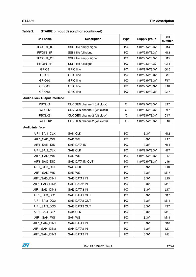
STA662 Pin description
Doc ID 023407 Rev 1 17/24
FIFOOUT_0E SSI 0 fifo empty signal I/O 1.8V/2.5V/3.3V H14
FIFOIN_1F SSI 1 fifo full signal I/O 1.8V/2.5V/3.3V H13
FIFOOUT_2E SSI 2 fifo empty signal I/O 1.8V/2.5V/3.3V H15
FIFOIN_3F SSI 3 fifo full signal I/O 1.8V/2.5V/3.3V G14
GPIO8 GPIO line I/O 1.8V/2.5V/3.3V G15
GPIO9 GPIO line I/O 1.8V/2.5V/3.3V G16
GPIO10 GPIO line I/O 1.8V/2.5V/3.3V F17
GPIO11 GPIO line I/O 1.8V/2.5V/3.3V F16
GPIO12 GPIO line I/O 1.8V/2.5V/3.3V G17
Audio Clock Output Interface
PBCLK1 CLK GEN channel1 (bit clock) O 1.8V/2.5V/3.3V E17
PWSCLK1 CLK GEN channel1 (ws clock) O 1.8V/2.5V/3.3V D17
PBCLK2 CLK GEN channel2 (bit clock) O 1.8V/2.5V/3.3V C17
PWSCLK2 CLK GEN channel2 (ws clock) O 1.8V/2.5V/3.3V E16
Audio interface
AIF1_SAI1_CLK SAI1 CLK I/O 3.3V N12
AIF1_SAI1_WS SAI1 WS I/O 3.3V T17
AIF1_SAI1_DIN SAI1 DATA IN I/O 3.3V N14
AIF1_SAI2_CLK SAI2 CLK I/O 1.8V/2.5V/3.3V H17
AIF1_SAI2_WS SAI2 WS I/O 1.8V/2.5V/3.3V J17
AIF1_SAI2_DIO SAI2 DATA IN-OUT I/O 1.8V/2.5V/3.3V J16
AIF1_SAI3_CLK SAI3 CLK I/O 3.3V L16
AIF1_SAI3_WS SAI3 WS I/O 3.3V M17
AIF1_SAI3_DIN1 SAI3 DATA1 IN I/O 3.3V L15
AIF1_SAI3_DIN2 SAI3 DATA2 IN I/O 3.3V M16
AIF1_SAI3_DIN3 SAI3 DATA3 IN I/O 3.3V L17
AIF1_SAI3_DO1 SAI3 DATA1 OUT I/O 3.3V N17
AIF1_SAI3_DO2 SAI3 DATA2 OUT I/O 3.3V M14
AIF1_SAI3_DO3 SAI3 DATA3 OUT I/O 3.3V P17
AIF1_SAI4_CLK SAI4 CLK I/O 3.3V M10
AIF1_SAI4_WS SAI4 WS I/O 3.3V M11
AIF1_SAI4_DIN1 SAI4 DATA1 IN I/O 3.3V N10
AIF1_SAI4_DIN2 SAI4 DATA2 IN I/O 3.3V M9
AIF1_SAI4_DIN3 SAI4 DATA3 IN I/O 3.3V M8
Table 2. STA662 pin-out description (continued)
Ball name Description Type Supply groupBall
number
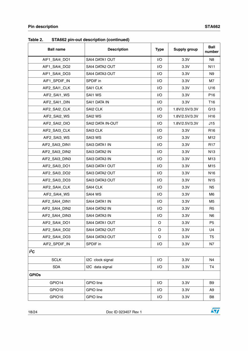
Pin description STA662
18/24 Doc ID 023407 Rev 1
AIF1_SAI4_DO1 SAI4 DATA1 OUT I/O 3.3V N8
AIF1_SAI4_DO2 SAI4 DATA2 OUT I/O 3.3V N11
AIF1_SAI4_DO3 SAI4 DATA3 OUT I/O 3.3V N9
AIF1_SPDIF_IN SPDIF in I/O 3.3V M7
AIF2_SAI1_CLK SAI1 CLK I/O 3.3V U16
AIF2_SAI1_WS SAI1 WS I/O 3.3V P16
AIF2_SAI1_DIN SAI1 DATA IN I/O 3.3V T16
AIF2_SAI2_CLK SAI2 CLK I/O 1.8V/2.5V/3.3V G13
AIF2_SAI2_WS SAI2 WS I/O 1.8V/2.5V/3.3V H16
AIF2_SAI2_DIO SAI2 DATA IN-OUT I/O 1.8V/2.5V/3.3V J15
AIF2_SAI3_CLK SAI3 CLK I/O 3.3V R16
AIF2_SAI3_WS SAI3 WS I/O 3.3V M12
AIF2_SAI3_DIN1 SAI3 DATA1 IN I/O 3.3V R17
AIF2_SAI3_DIN2 SAI3 DATA2 IN I/O 3.3V N13
AIF2_SAI3_DIN3 SAI3 DATA3 IN I/O 3.3V M13
AIF2_SAI3_DO1 SAI3 DATA1 OUT I/O 3.3V M15
AIF2_SAI3_DO2 SAI3 DATA2 OUT I/O 3.3V N16
AIF2_SAI3_DO3 SAI3 DATA3 OUT I/O 3.3V N15
AIF2_SAI4_CLK SAI4 CLK I/O 3.3V N5
AIF2_SAI4_WS SAI4 WS I/O 3.3V M6
AIF2_SAI4_DIN1 SAI4 DATA1 IN I/O 3.3V M5
AIF2_SAI4_DIN2 SAI4 DATA2 IN I/O 3.3V R5
AIF2_SAI4_DIN3 SAI4 DATA3 IN I/O 3.3V N6
AIF2_SAI4_DO1 SAI4 DATA1 OUT O 3.3V P5
AIF2_SAI4_DO2 SAI4 DATA2 OUT O 3.3V U4
AIF2_SAI4_DO3 SAI4 DATA3 OUT O 3.3V T5
AIF2_SPDIF_IN SPDIF in I/O 3.3V N7
I2C
SCLK I2C clock signal I/O 3.3V N4
SDA I2C data signal I/O 3.3V T4
GPIOs
GPIO14 GPIO line I/O 3.3V B9
GPIO15 GPIO line I/O 3.3V A9
GPIO16 GPIO line I/O 3.3V B8
Table 2. STA662 pin-out description (continued)
Ball name Description Type Supply groupBall
number
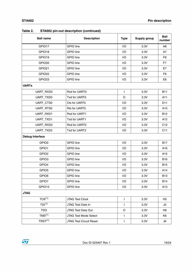
STA662 Pin description
Doc ID 023407 Rev 1 19/24
GPIO17 GPIO line I/O 3.3V A8
GPIO18 GPIO line I/O 3.3V A7
GPIO19 GPIO line I/O 3.3V F8
GPIO20 GPIO line I/O 3.3V F7
GPIO21 GPIO line I/O 3.3V E7
GPIO22 GPIO line I/O 3.3V F6
GPIO23 GPIO line I/O 3.3V E6
UARTs
UART_RXD0 Rxd for UART0 I 3.3V B11
UART_TXD0 Txd for UART0 O 3.3V A11
UART_CTS0 Cts for UART0 I/O 3.3V D11
UART_RTS0 Rts for UART0 I/O 3.3V A10
UART_RXD1 Rxd for UART1 I/O 3.3V B12
UART_TXD1 Txd for UART1 I/O 3.3V A12
UART_RXD2 Rxd for UART2 I/O 3.3V C12
UART_TXD2 Txd for UART2 I/O 3.3V C11
Debug Interface
GPIO0 GPIO line I/O 3.3V B17
GPIO1 GPIO line I/O 3.3V A16
GPIO2 GPIO line I/O 3.3V A15
GPIO3 GPIO line I/O 3.3V B16
GPIO4 GPIO line I/O 3.3V B15
GPIO5 GPIO line I/O 3.3V A14
GPIO6 GPIO line I/O 3.3V B13
GPIO7 GPIO line I/O 3.3V B14
GPIO13 GPIO line I/O 3.3V A13
JTAG
TCK(1) JTAG Test Clock I 3.3V H5
TDI(1) JTAG Test Data In I 3.3V J5
TDO JTAG Test Data Out O 3.3V H6
TMS(1) JTAG Test Mode Select I 3.3V K6
TRST(1) JTAG Test Circuit Reset I 3.3V J6
Table 2. STA662 pin-out description (continued)
Ball name Description Type Supply groupBall
number
Pin description STA662
20/24 Doc ID 023407 Rev 1
Antenna switching
AS0 Antenna switching selector bit 0 O 3.3V A4
AS1 Antenna switching selector bit 1 O 3.3V B4
System level signals
CLKSEL0 Clock mode selector bit 0 I 3.3V E13
CLKSEL1 Clock mode selector bit 1 I 3.3V E14
MCLKOUT System clock out O 3.3V D15
BOOTSEL0 Boot selector bit 0 I 3.3V D14
BOOTSEL1 Boot selector bit 1 I 3.3V D13
RESET_N(1),(2) System reset input I 3.3 V C14
IOPSW0 Pad ring power supply selector bit 0 I 3.3V L5
IOPSW1 Pad ring power supply selector bit 1 I 3.3V L6
TESTSEL0 Test mode selector bit 0 I 3.3V C13
TESTSEL1 Test mode selector bit 1 I 3.3V E12
TESTSEL2 Test mode selector bit 2 I 3.3V D12
TESTSEL3 Test mode selector bit 3 I 3.3V E11
DRAM_ENABLE(3) Dram interface enable I 3.3V F10
XTAL
XTI OSCI input Analog - E8
XTO OSCI output Analog - E9
AVDD2V5_OSCI30 OSCI analog power supply PWR 2.5V D9
AGNDSUB_OSCI30 OSCI analog ground GND - D8
AVDD1V2_OSCI30 OSCI digital power supply PWR 1.2V D10
AGND_OSCI30 OSCI digital ground GND - E10
2.5 Volt LDO
LDO2V5LDO regulator 2.5 V output power supply
PWR - C6
PLLs Power supply and ground signal
DVDD_SYSPLL PLLs Digital Power supply PWR 1.2V A6
DGND_SYSPLL PLLs Digital Power ground GND - B6
AVDD_SYSPLL PLLs Analog Power supply PWR 2.5V A5
AGND_SYSPLL PLLs Analog Power ground GND - B5
DVDD_AUDPLL PLLs Digital Power supply PWR 1.2V B7
Table 2. STA662 pin-out description (continued)
Ball name Description Type Supply groupBall
number
STA662 Pin description
Doc ID 023407 Rev 1 21/24
2.3 Pins terminationIn order to guarantee the correct behavior of an STA662 based application it is mandatory to properly terminate unused input and inout pins.
Since many of the STA662 pins have secondary/tertiary functions which depend on the specific firmware configuration, it is strongly suggested to review the final application's schematic with ST application engineer.
DGND_AUDPLL PLLs Digital Power ground GND - D7
AVDD_AUDPLL PLLs Analog Power supply PWR 2.5V C7
AGND_AUDPLL PLLs Analog Power ground GND - D6
Power Supply and Ground Signals (73 I/O)
GNDE Pad ring ground GND -
G6, G8, G11,
J11, L8, P11
VDDE 3.3 V pad power supply PWR 3.3V
F9, G10, H7,
H11, K7, L9,
L11
VDDE_3P Triple voltage pad power supply PWR 1.8V/2.5V/3.3VH12, J12
GND / GNDS Digital ground GND -
A1, A17, H8, H9, H10, J8, J9, J10, K8, K9,
K10, K13
VDD / VDDS Digital power supply PWR 1.2V
F11, G7, G9, G12, J7,
K11, K12, L7,
L10, L12, U1,
U17
1. Smidth trigger input pad.
2. Pull down pad.
3. The DRAM_ENABLE pin must be set to logical one at PCB level.
Table 2. STA662 pin-out description (continued)
Ball name Description Type Supply groupBall
number
Package information STA662
22/24 Doc ID 023407 Rev 1
3 Package information
In order to meet environmental requirements, ST offers these devices in different grades of ECOPACK® packages, depending on their level of environmental compliance. ECOPACK® specifications, grade definitions and product status are available at: www.st.com.
ECOPACK® is an ST trademark.
Figure 5. TFBGA289 mechanical data and package dimensions
STA662 Revision history
Doc ID 023407 Rev 1 23/24
4 Revision history
Table 3. Document revision history
Date Revision Changes
06-Jul-2012 1 Initial release.
STA662
24/24 Doc ID 023407 Rev 1
Please Read Carefully:
Information in this document is provided solely in connection with ST products. STMicroelectronics NV and its subsidiaries (“ST”) reserve theright to make changes, corrections, modifications or improvements, to this document, and the products and services described herein at anytime, without notice.
All ST products are sold pursuant to ST’s terms and conditions of sale.
Purchasers are solely responsible for the choice, selection and use of the ST products and services described herein, and ST assumes noliability whatsoever relating to the choice, selection or use of the ST products and services described herein.
No license, express or implied, by estoppel or otherwise, to any intellectual property rights is granted under this document. If any part of thisdocument refers to any third party products or services it shall not be deemed a license grant by ST for the use of such third party productsor services, or any intellectual property contained therein or considered as a warranty covering the use in any manner whatsoever of suchthird party products or services or any intellectual property contained therein.
UNLESS OTHERWISE SET FORTH IN ST’S TERMS AND CONDITIONS OF SALE ST DISCLAIMS ANY EXPRESS OR IMPLIEDWARRANTY WITH RESPECT TO THE USE AND/OR SALE OF ST PRODUCTS INCLUDING WITHOUT LIMITATION IMPLIEDWARRANTIES OF MERCHANTABILITY, FITNESS FOR A PARTICULAR PURPOSE (AND THEIR EQUIVALENTS UNDER THE LAWSOF ANY JURISDICTION), OR INFRINGEMENT OF ANY PATENT, COPYRIGHT OR OTHER INTELLECTUAL PROPERTY RIGHT.
UNLESS EXPRESSLY APPROVED IN WRITING BY TWO AUTHORIZED ST REPRESENTATIVES, ST PRODUCTS ARE NOTRECOMMENDED, AUTHORIZED OR WARRANTED FOR USE IN MILITARY, AIR CRAFT, SPACE, LIFE SAVING, OR LIFE SUSTAININGAPPLICATIONS, NOR IN PRODUCTS OR SYSTEMS WHERE FAILURE OR MALFUNCTION MAY RESULT IN PERSONAL INJURY,DEATH, OR SEVERE PROPERTY OR ENVIRONMENTAL DAMAGE. ST PRODUCTS WHICH ARE NOT SPECIFIED AS "AUTOMOTIVEGRADE" MAY ONLY BE USED IN AUTOMOTIVE APPLICATIONS AT USER’S OWN RISK.
Resale of ST products with provisions different from the statements and/or technical features set forth in this document shall immediately voidany warranty granted by ST for the ST product or service described herein and shall not create or extend in any manner whatsoever, anyliability of ST.
ST and the ST logo are trademarks or registered trademarks of ST in various countries.
Information in this document supersedes and replaces all information previously supplied.
The ST logo is a registered trademark of STMicroelectronics. All other names are the property of their respective owners.
© 2012 STMicroelectronics - All rights reserved
STMicroelectronics group of companies
Australia - Belgium - Brazil - Canada - China - Czech Republic - Finland - France - Germany - Hong Kong - India - Israel - Italy - Japan - Malaysia - Malta - Morocco - Philippines - Singapore - Spain - Sweden - Switzerland - United Kingdom - United States of America
www.st.com