Embed Size (px)
Citation preview

A Modified Space Vector PWM for Z-Source Inverter - Modeling and Design
Jingbo Liu, Student Member IEEE, Jiangang Hu and Longya Xu, Fellow IEEEDepartment of Electrical and Computer Engineering,
The Ohio State University205 Dreese Lab, 2015 Neil Ave., Columbus OH 43210, U.S.A.
Abstract In this paper, an AC small-signal equivalentcircuit model of continuous conduction mode (CCM) ZSIbased on state space averaging is presented. The AC small-signal model includes the dynamics of ZSI introduced by theinductors and capacitors contained in the ZSI circuit, pro-viding guidelines to the system control design. In addition, anovel modified space vector PWM is presented to distributethe shoot-through states into the zero vectors without com-promise to the active space vector. Simulation results basedon the design are presented, using the proposed SVPWMcontrol strategy.
I. INTRODUCTION
Conventional Voltage Source Inverters (VSI) and Cur-rent Source Inverters (CSI) are commonly used as thepower electronic circuit for AC machine drives. A con-ventional VSI is a DC-AC buck inverter (or AC-DC boostrectifier) while a conventional CSI a DC-AC boost in-verter (or AC-DC buck rectifier). For applications suchas the AC drive system requiring the machine operatingover a wide speed range, it is much preferable that thepower converter has the buck-boost capability. A newtype of power converter, i.e. Z source inverter (ZSI), withbuck-boost capabilities has been recently proposed andstudied [1]-[5]. The AC voltage from ZSI can be con-trolled theoretically to any value. It is apparent that theZSI can give a large degree of freedom to AC machinedesign and control so that the performance and costs ofoverall AC drive system is optimized [5].
To design proper control for ZSI powered system, weneed a proper dynamic model of ZSI for its switchingoperation. We will extend the steady state model of ZSI[1]-[5] to include the dynamics introduced by the induc-tors and capacitors contained in the circuit. In this paper,an AC small-signal equivalent circuit model ofCCM ZSIbased on state space averaging is presented. The small-signal modeling of ZSI also provides guidelines to thesystem control design since the transfer functions couldbe derived accordingly. Simulation results obtained bythe switching ZSI are presented, backed up with the simu-lation results using averaging modeling method.
Space vector pulse width modulation (SVPWM) iswidely used for variable frequency drive applications be-cause of its various advantages such as the good DC utili-zation and less harmonics distortion in the output wave-form. In order to use SVPWM for ZSI, conventionalspace vector control strategy has to be changed to distrib-ute the shoot-through states into the zero vectors withoutcompromise to the active space vector. In this paper, anovel modified space vector is presented for the control ofZSI as shown in Fig. 1. Simulation results are presented
using the proposed SVPWM control strategy and designdetails are provided in the paper.DC Source or Load Z Network vsI
Figure 1. Structure of a VSI-based Z-Source Converter
II. AC SMALL SIGNAL MODELING OF Z CONVERTER
A. AC Small Signal Modeling ofZ Converter Operatingin CCMBased on State Space Averaging
Operation of ZSI can be illustrated by simplifying theAC side of the circuit to a DC load (or source) as shown inFig. 2. Two operation modes can be identified in ZSI op-eration as shown in Fig. 3 and Fig. 4. In the simplifiedcircuit, the load to the ZSI inverter bridge is viewed as anequivalent load in parallel with an active switch S2. Theequivalent circuit of the Z network could be viewed as aDC-DC converter. In the modeling and analysis presentedin this paper, we assume that Z converter is operating inCCM.
VLI - L
TLI
VL2
Figure 2. Equivalent circuit of Z-source inverter
In Mode 1 operation as shown in Fig. 3, energy trans-ferred from source to load equals to zero because the loadside and source side are essentially decoupled by theshoot-through states and the open status of Si. The dutyratio D of switch S2 is the so-called shoot-through ratio.
We define the state vector as:
iL (t)
x(f)=r )(1
VcI (t)VC 2(e
1242
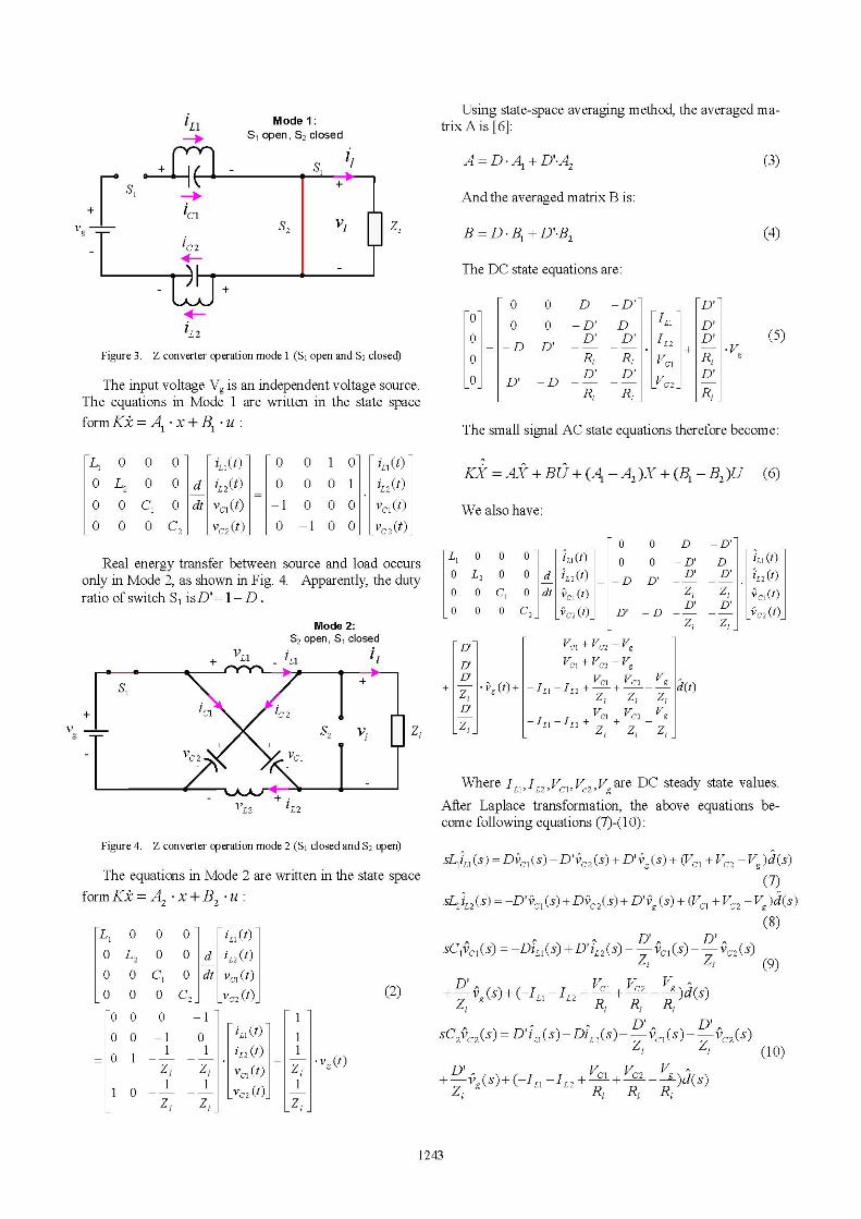
IL1 Mode 1:S1 open, S2 closed
Using state-space averaging method, the averaged ma-trix A is [6]:
A =D Al +D'A2 (3)
And the averaged matrix B is:
B=D B1+D'*B2
The DC state equations are:
IL2Figure 3. Z converter operation mode 1 (S1 open and S2 closed)
The input voltage Vg is an independent voltage source.The equations in Mode 1 are written in the state spaceformKx=A1 x+B( u:
00O
O=
D0
o Di
O D
O - D'o D'D
RI- D -
D
RI
- D' Di
D ILi D,D' I1D2
+ v
RI VC RI
D1 Di
The small signal AC state equations therefore become:
0 iLI(t) 0
0 d iL2(t) 0
0 dt vcl (t) - 1
C2 vC2(t)_ - 0
0 1 0 -iLl (t)-
0 0 1 .L 2 (t)
0 0 0 vcl (t)-1 0 0 -vC2(t)
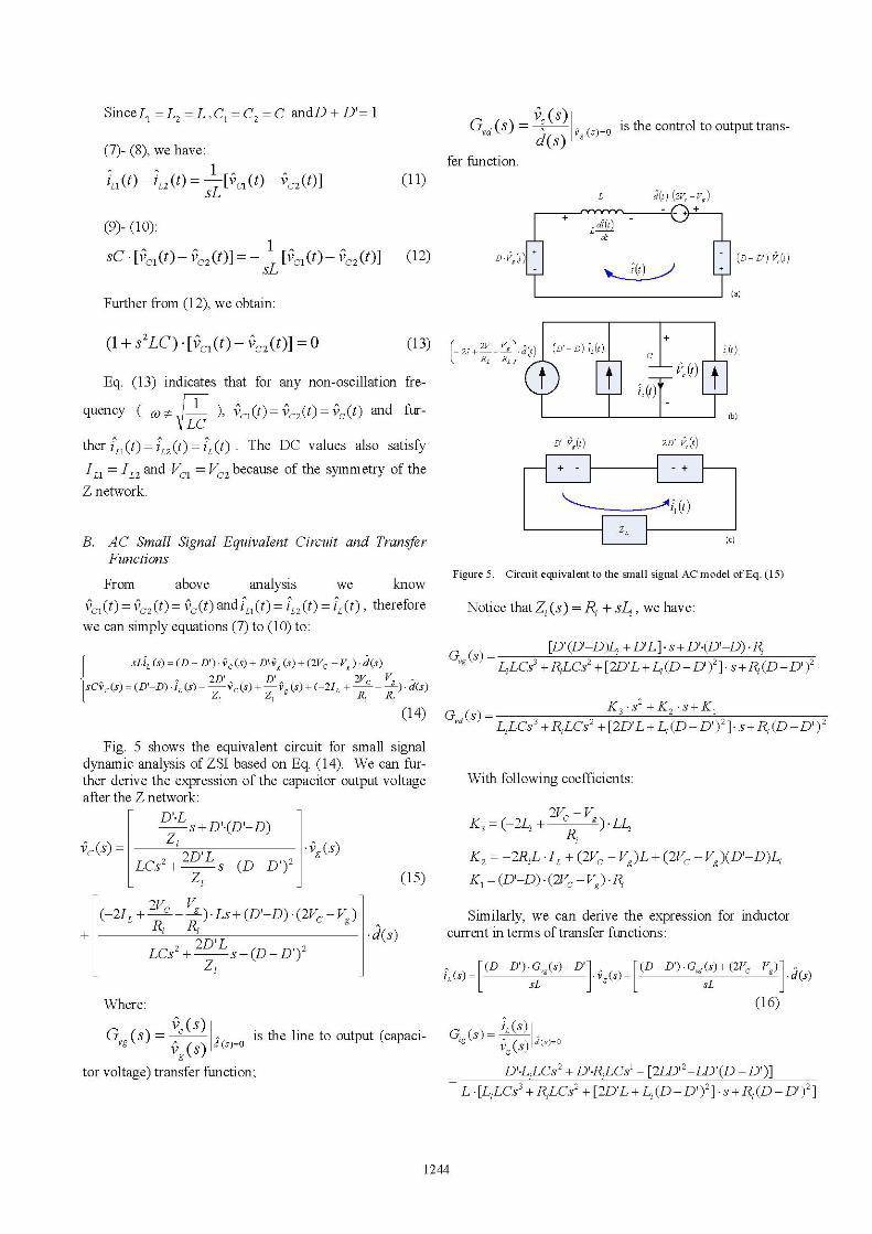
Real energy transfer between source and load occursonly in Mode 2, as shown in Fig. 4. Apparently, the dutyratio of switch S1 is D'= 1 - D.
KX=AX+BU+(Al-A2)X+(B1-B2)U (6)
We also have:
Li000
0
L200
0
0
Ci0
Mode 2:S2 open, S1 closed
il
± zi
Iz
vg
ILI
ILI
0 iL1 (t)Od IL2(t)0 dt|cl (t))C2 _vC2 (t)
00
- -D
Dv
O DO -D'Dv D'
zi
-D -
zi
D iL1 (t)D' iL2 (t)
I vcl (t)
zI-
VcI + VC2 Vg
VcI + VC2 Vg
- IL + VCI + VC2 _ Vg d(t)L±I IL2
z z zI I Il,
_% _-+
VL2 'L2
Figure 4. Z converter operation mode 2 (SI closed and S2 open)
The equations in Mode 2 are written in the state space
form Kx=A2 x+B2 u:
-Li
0
0
0
0
0
=OO
0
L2
0
0
0
1
0
0
0
Cl
0
0
-1II
ziI
_i
0 iLl (t)
O d iL2 (t)O dt vcl (t)
C2 - _VC2 (t)-1I - I
0 iLl (t) 1
1L2 (t)
--I . t(2((tt)+ Z, vg (t)1I LVC2(t) Z1
VC2(t)
1z
Where VL iL2'v V are DC steady state values.IL1L ' Cl' c2'
After Laplace transformation, the above equations be-come following equations (7)-(10):
sLiLi(s) Dic (s) - D'VC2(S) + D vg(S) + (VCI + VC2- Vg)d(s)
(7)sL2iL2 (s) -D'ci (s) + DVC2 (S) + D'ig (s) + (Vc1 + VC2 - Vg)d(s)
(8)
SC,Vc, (s) = -DiLi (s) + D'iL2(s) --vc, (s) --VC2 (s)Z/ Z/ (9)
(2) +-v (s) + (-,LI - IL2 +R + C2 _ )d(s)z 9 ~R1 RI RI
C2VC2 (S) = D' js) - DIL2 (S ) -- CI (S ) -- C2 (S)Z, Z, (10)
+ -3v(s) +(-,LI - IL2 + + CR - g)d(s)Z, RI~~ RI RI
1243
+Ivg Zi (4)
0
L200
-LI0
00
00
Cl
0
(5)
+ VL_ 1 - iLl
Gvd (s) = ( (S)=O is the control to output trans-df(s) VgQ)i0
fer function.(7)- (8), we have:
'LI (t) L2(t) = [VII(t)(-C2(0sL
(9)- (10):sC [Icl (t)-VC2(- = -- cl (t)-VC2 (01
(1 1)
(12)
Further from (12), we obtain:
(I + S2 LC) - [V^ v ~~~(13) 212VV(1+sL) [cl(t) C2(0)] = O ( -2I+-RL RL
Eq. (13) indicates that for any non-oscillation fre-
quency ( ac ), v<1(t) =vC2(t) =vC(t) and fur-LC
ther l(t) iL2(t) IL(t) The DC values also satisfy
ILI = IL2 and VCI = VC2 because of the symmetry of theZ network.
B. AC Small Signal Equivalent Circuit and TransferFunctions
From above analysis we know
<1l (t) = 3c2(t) = 3C (t) and IL1 () iL2(t) IL(t), thereforewe can simply equations (7) to (10) to:
SLIL (S) = (D - D') ic (s) + D' vg (s) + (2Vc Vg) *d(s)sCvc(s) =(D'-D) iL(s)- 'C(s)± Dg(s)+(-21L + )d(s)
Z R R
(14)
Fig. 5 shows the equivalent circuit for small signaldynamic analysis of ZSI based on Eq. (14). We can fur-ther derive the expression of the capacitor output voltageafter the Z network:
ic3(s) = -
DlLs + D'.(D'-D)
LCs2 +2D'L2LC 2+2D'S+(D D')2
ZI
V9g(s)
(15)
D'.*V (t) 2D'.V (t)
11 (t)
(c)
Figure 5. Circuit equivalent to the small signal AC model of Eq. (15)
Notice that Z, (s) = RI + sL,, we have:
G (s) [D'(D'-D)L, + D'L] s + D'.(D'-D). RIL,LCs3 + RLCs2 + [2D'L + LI(D - D')2] s+R(D_ D')2
Gd(s)- K3 s2 +K2 s+KlLLCs3+RILCs +[2D'L+L,(D-D')]*s+R,(D-D')2
With following coefficients:
K3 ( 2L1+ 2Vc - Vg LLRI
K22 -2RIL ILL+ (2VC - VK1 = (D'-D) .(2VC - Vg) RI
'g)L + (2Vc - Vg)(D'-D)L,
2V V
(-2IL+-4 gR) LS+(D'-D) .(2VC -Vg)RIC RI
L s +(D -D')2)
Where:
Gvg (s) = ^ () 0d()O is the line to output (capaci-t()dsfu
tor voltage) transfer function;
Similarly, we can derive the expression for inductorcurrent in terms of transfer functions:
i (s (D - D ) G'g(s) + D'1v(s+ (D - D ) GVd (s) + (2Vc - Vg); (
(16)
Gig(S) =iL
'lg(S) d(s)=0
D' L LCs2 + D' RLCs' + [2LD'2+LD'(D - D')]L [LILCs3 + RILCs2 + [2D'L + LI(D - D')2] s + RJ(D - D')2]
1244
SinceL =L2 =L,C =C2=C andD+D'=1
(D -D')*V(t)
4- L---LL--Lj

dL(s)Gda(s)= d(s | v( 0
K6s2 +K5s+K4L .[LiLCs3 +RILCs2 +[2D'L +L1(D -D')2ss+R(D -D')2]
Bode Diaaram of the input-to-outputtransferfunction GvgSystem A
)q.er,cy (Hz): 204gn,itude (dB): 15.7 _ _ _ _ _ _ _ _ ____L1:150uH
L2:300uHL Increase-
L3:400uH
X4----A X L4:500 uH
Coefficients K4 to K6 are:
K6 (2VC -Vg) LiLC;
K5 (2Vc - Vg)yRLC- (D- D') 2LILIh+ (D D') C LIL
K4 (2VC -Vg)-L- 2R1L11
Having found the analytical expressions of the abovetransfer functions, we can obtain the Bode plots suppos-ing we are given with the following values: Vg 1501KRIl12ohm, L,=O. lmH and shoot-through ratio D=0.3.
The salient feature of transfer functions of Bode plotscan help us design the parameters of L and C in the Znetwork. For instance, Fig. 6 shows the parameter sweepof C in the Z network if inductances are chosen as 300uH.Another parameter sweep results of different inductancesare shown in Fig. 7 with 330uF capacitances. Thereforein the presented design, L is chosen as 300uH and C as160uF. With such parameters used, the input-to-outputtransfer function has a DC gain of 4.86dB (1.75), resonantpole of 203Hz having a Q of 10.74dB.
L1:150uH
_ L2:300uH 4
L3:400uH
L4:500uH C<\ System:A\ Phas Margin, (deg):i\ gDelay Margimn(sec):I
- ->\ Atfrequency (Hz): .,\S Closed Loop Stable?
Frequency (Hz)
Figure 7. Bode plot of input-to-output transfer function Gvg, Zconverter with different inductances
Indct CUIeft by swIldng cOWS rnoel aX taoe clrcWtii 4l..................RA.. ..... .............. ..... ....................... .. ........... ....
so aJlilll dfitllX SW1Ikhbig l tSte imrdi
_Xi'0 dll40[ X
< 4 Wfil4WlmWW $#zfl2-gW 03~~~~~~tccW gltaiypg: rXl
Bode Diagram of the input-to-outputtransferfunction Gvg
-C IncreaseS
AH P- 40-f IceaeIgE
XiH - \TT -!-'
- C1:220uF
- C2:33OuF
C3:47OuF
C4:1OOOuF
C1:220uF
C2:33OuF
C3:47OuF
C4:10OOuF
vvf 0.
Figure 8. Simulation results by switching circuit model (shown inFig.2) and average circuit model (shown in Fig. 5): inductor currents
Frequency (Hz)
Figure 6. Bode plot of input-to-output transfer function Gvg, Zconverter with different capacitances
Fig. 8 and 9 show the simulation results by the switch-ing circuit model (shown in Fig. 2) and average circuitmodel (shown in Fig. 5). Fig. 8 shows the simulationresults of capacitor voltages of the Z network (VC1 and V,2in Fig. 2) while Fig. 9 shows the results of inductor cur-rents (IL, and IL2 in Fig. 2). As show in the figures, thesteady state value of the boosted DC voltage by Z net-work is 262.5V, perfectly matching the expected valuewith the DC gain of 1.75 (shoot-through ratio 0.3).
Apparently, the proposed averaged circuit model for Zconverter is proven to be accurate enough to predict con-verter dynamic responses as well as steady state valueswhen operating in CCM.
V949 .X 0.049 '7 10493 0.049
Figure 9. Simulation results by switching circuit model (shown in
Fig.2) and average circuit model (shown in Fig. 5): capacitor voltages
1245
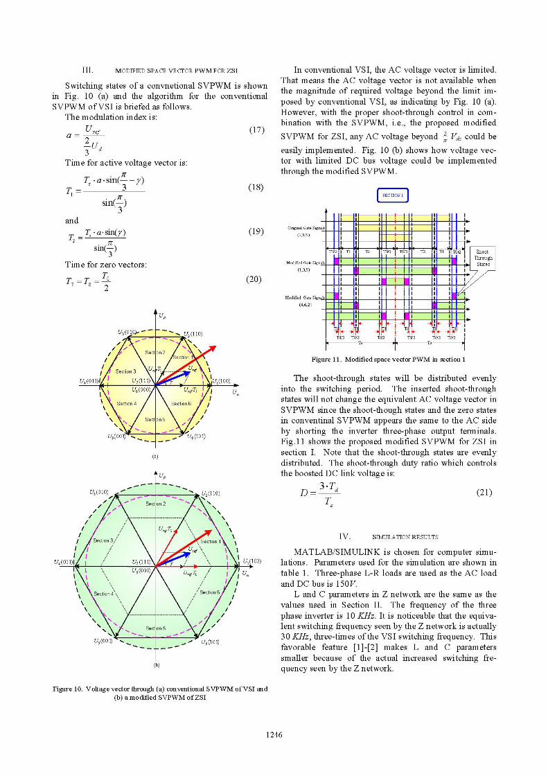
III. MODIFIED SPACE VECTOR PWM FOR ZSI
Switching states of a convnetional SVPWM is shownin Fig. 10 (a) and the algorithm for the conventionalSVPWM ofVSI is briefed as follows.
The modulation index is:
aU ref
2U3d
Time for active voltage vector is:
Ts -a sin( -y)T = 3
In conventional VSI, the AC voltage vector is limited.That means the AC voltage vector is not available whenthe magnitude of required voltage beyond the limit im-posed by conventional VSI, as indicating by Fig. 10 (a).However, with the proper shoot-through control in com-bination with the SVPWM, i.e., the proposed modifiedSVPWM for ZSI, any AC voltage beyond 2 Vd, could beeasily implemented. Fig. 10 (b) shows how voltage vec-tor with limited DC bus voltage could be implementedthrough the modified SVPWM.
sin(W)3
and
T T, . a. sin(y)sin(-)3
Time for zero vectors:
TTT7 =T8 =2
(19)
(20)
t U
Td Td Td !T Td Td1W 4 4: 0 4 A 4 0. 4 14
Td/2 Td/2 Td/2 Td/2 Td/2 Td/2Fiur* .M e c o P Ts e 1
Figure I11. Modified space vector PWM in section I
The shoot-through states will be distributed evenlyinto the switching period. The inserted shoot-throughstates will not change the equivalent AC voltage vector inSVPWM since the shoot-though states and the zero statesin conventinal SVPWM appears the same to the AC sideby shorting the inverter three-phase output terminals.Fig.11 shows the proposed modified SVPWM for ZSI insection I. Note that the shoot-through states are evenlydistributed. The shoot-through duty ratio which controlsthe boosted DC link voltage is:
D- !d (21)TS
IV. SIMULATION RESULTS
MATLAB/SIMULINK is chosen for computer simu-U1(100) lations. Parameters used for the simulation are shown inua table 1. Three-phase L-R loads are used as the AC load
and DC bus is 150 V.L and C parameters in Z network are the same as the
values used in Section II. The frequency of the threephase inverter is 10 KHz. It is noticeable that the equiva-lent switching frequency seen by the Z network is actually30 KHz, three-times of the VSI switching frequency. Thisfavorable feature [1]-[2] makes L and C parameterssmaller because of the actual increased switching fre-quency seen by the Z network.
Figure 10. Voltage vector through (a) conventional SVPWM of VSI and(b) a modified SVPWM of ZSI
1246
U4(011 U1(100)N
U,y
(a)
tU
U4 (0
(b)
II

TABLE I. PARAMETERS USED FOR COMPUTER SIMULATIONS
Parameter Value
Inductors (Ld,) in DC link 300upH
Capacitors (Ce) in DC link 33OpF
DC bus 150 V
DC Link boost factor (J-D)1(J-2D) 1.75
AC side Load inductance 8 mH
AC side Load resistance 0.9 ohm
Switching frequency 10 kHz
Fundamental frequency 60 Hz
Simulation results for the proposed modified SVPWMare shown in Fig. 12 to Fig. 14. Fig. 12 shows the ACphase currents flowing in the loads. Fig. 13 shows theAC phase voltages and Fig. 14 is the FFT result for theAC phase voltages.
Figure 14.FFT ResUlt of phase Avoltage
SImuaineutGso ht h C ikvltg a
peak alue Figr 4Ffudaenuta AC phaseAvoltage i bu
140V, much beyond the limit imposed by conventional
VSI (2 -150o::~95.5V)./IT
V. CONCLUSIONS AND FUTURE WORK
Figure 12. Simulation results of AC phase currents
Figure 13. Simulation results of AC phase voltages
The AC small signal modeling of Z source converteris firstly proposed in this paper, giving analytical methodas well as design guidelines. Moreover, a novel modifiedspace vector PWM for voltage-fed ZSI suitable for vari-able frequency AC drives has been proposed in this paper.With the proposed modified SVPWM, the AC voltageobtainable from ZSI is no longer limited and can beboosted beyond the limit imposed by conventional VSI.Simulation results verified the effectiveness of the pro-posed small signal modeling of ZSI and also the modifiedSVPWM control strategy. More detailed results in mod-eling and implementations of voltage-fed ZSI for adjust-able speed AC drives will be provided in future publica-tions, backed up with experimental investigations.
REFERENCES
[1] Peng, F.Z., '7-source inverter", IEEE IAS Conference, Vol.2, pp775 -781, 2002.[2] Peng, F.Z., Xiaoming Yuan, Xupeng Fang and Zhaoming Qian,'7-source inverter for adjustable speed drives", Power ElectronicsLetters, IEEE, Volume: 1 Issue: 2 ,June 2003, pp. 33 -35.
[3] Peng, F.Z., "Z-source inverter for motor drives "IEEE PowerElectronics Specialists Conference, PESC 2004, pp 249 -254.
[4] Longya Xu and Jingbo Liu, "Comparison study of DC- DC-ACcombined converters for integrated starter generator applications", IEEEPower Electronics and Motion Control Conference, IPEMC 2004, Aug.14-16 2004, Vol.3, pp 1130 -1135.[5] Poh Chiang Loh; Vilathgamuwa, D.M.; Yue Sen Lai;, Geok Tin
Chua;Yunwei I,"uswitmolaIono -oreivres,IE
39th IAS Annual Meeting. Conference Record of the 2004, Vo. 1 ,2004,pp. 148-155.
[6] Robert W. Erickson and Dragan Maksimovic, "Fundamentals ofPower Electronics (2ndEd.)", Kluwer Academic Pub., 2001.
1247


![L19 [Acon] Esquema eléctrico](https://img.pdfslide.net/doc/110x75/62c49c06196c397f48663d8e/l19-acon-esquema-elctrico.jpg)