Embed Size (px)
Citation preview

Amplitude and Phase Modulation Techniques for an
Asymmetric Multi-Level Outphasing Transmitter
by
Gilad Yahalom
Submitted to the Department of Electrical Engineering and ComputerScience
in partial fulfillment of the requirements for the degree of
Master of Science in Electrical Engineering
at the
MASSACHUSETTS INSTITUTE OF TECHNOLOGY
ARCHIVESITUTE
2131
September 2012
@ Massachusetts Institute of Technology 2012. All rights reserved.
A uthor . . . .................... ....................Department of Electrical Engineering and Computer Science
Aug 29, 2012
Certifiedby.........,.. .......
Joel L. DawsonAssociate Professor
Thesis Supervisor
Accepted by .......................Leshb(OA.(kolodziej ski
Chairman, Department Committee on Graduate Theses

2

Amplitude and Phase Modulation Techniques for an Asymmetric
Multi-Level Outphasing Transmitter
by
Gilad Yahalom
Submitted to the Department of Electrical Engineering and Computer Scienceon Aug 29, 2012, in partial fulfillment of the
requirements for the degree ofMaster of Science in Electrical Engineering
Abstract
New techniques for improving outphasing transmitters show potential of breaking the tra-ditional linearity-efficiency trade-off by using highly efficient non-linear switching PowerAmplifiers (PAs). This work focuses on two of the main building blocks of modem out-phasing systems, the power supply switching network and the phase modulator. Both areubiquitous building blocks in modern RF transceivers, and both are especially critical inAsymmetric Multilevel Outphasing (AMO) systems.
A design of the power supply network and control scheme is proposed for an imple-mentation in mm-wave operating frequencies as part of a complete transmitter in 45nmSOI CMOS utilizing four discrete power supplies and achieving data rates of up to 4GS/s.The design includes analysis and simulation of the control signal data path requirements foroptimal system operation as well as switch optimization and effects of the driving strengthon overall system performance.
A new design concept is proposed for a phase modulator utilizing the phase shifthingcapabilities of a resonant tank and the ability to seperately control the circuit propertiesvia its components. A prototype in 65nm CMOS achieves 12 bits of resolution, with anEffective Number Of Bits (ENOB) of 10.2 bits and very fast settling time of less than 5carrier cycles. The chip is also tested as a stand alone transmitter showing an EVM ofless than 5% for 8-PSK modulation at maximum data rate, meeting the requirements foroperation at the Medical Implant Communication Services (MICS) band.
Thesis Supervisor: Joel L. DawsonTitle: Associate Professor
3

4

Acknowledgments
I would like to thank Professor Joel Dawson for all his support during my work on this
Thesis and helping me along my journey so far through MIT. His encouragmenet and good
advice were invaluable to the success of this work. His wealth of knowledge and openess
to new ideas and directions allowed me to reach out and explore wider areas and branch
out to new directions and helped me overcome many of the hurdles along the way, all the
while creating a friendly and extremely pleasent work environment in his group.
I would also like to thank Professor Vladimir Stojanovic, Professor David Ricketts and
Dr. Yehuda Avniel for many helpful discussions and reviews of the work, each highlighting
different aspects and helping realize better solutions with a broader system view.
My Colleague and teammates Taylor Barton, SungWon Chung, Zhen Li and Sushmit
Goswami for countless discussion and consoltations and having the patience to hear me
detail my problems and numerous bugs. I would also like to thank Philip Godoy and John
Spaulding whose research is the basis my work is laid upon. Yan Li and Zhipeng Li for
assisting and leading the digital side of the project and Wei Tai and Chongzhe Li for their
PA and combiner work, great help and many useful tips during layout and final tapeout.
I'd also like to thank Professor Anantha Chandrakasan who helped secure foundry ser-
vices from TSMC which enabled the realization of the proof-of-concept phase modulator
design presented in this work.
Finally, Nothing in my career could ever get done without the endless support and
patience from my lovely wife Emanuel - Thanks for being there for me and believing in
me.
And of course - thanks Mom and Dad
5

6

Contents
List of Figures 9
List of Tables 13
List of Acronyms 15
1 Introduction 17
1.1 Motivation. . . . . . . . . . . . . . . . . . . . . . . . . . . . . . . . . . . 17
1.2 Linear Transmitter . . . . . . . . . . . . . . . . . . . . . . . . . . . . . . 18
1.3 Polar Transmitter . . . . . . . . . . . . . . . . . . . . . . . . . . . . . . . 19
1.4 Outphasing Transmitter . . . . . . . . . . . . . . . . . . . . . . . . . . . . 21
1.5 Asymmetric Multilevel Outphasing (AMO) Transmitter . . . . . . . . . . . 22
1.6 Research Contributions . . . . . . . . . . . . . . . . . . . . . . . . . . . . 24
2 Amplitude Modulation 27
2.1 Introduction . . . . . . . . . . . . . . . . . . . . . . . . . . . . . . . . . . 27
2.2 Power Supply Switch Network . . . . . . . . . . . . . . . . . . . . . . . . 28
2.2.1 Switch Design . . . . . . . . . . . . . . . . . . . . . . . . . . . . 29
2.2.2 Time Alignment . . . . . . . . . . . . . . . . . . . . . . . . . . . 36
2.2.2.1 Nulling Test . . . . . . . . . . . . . . . . . . . . . . . . 38
2.2.3 Decoding and Overlap Control . . . . . . . . . . . . . . . . . . . . 40
2.2.4 Level Shifting . . . . . . . . . . . . . . . . . . . . . . . . . . . . . 42
2.2.5 Slew Rate Control . . . . . . . . . . . . . . . . . . . . . . . . . . 45
2.3 Summary . . . . . . . . . . . . . . . . . . . . . . . . . . . . . . . . . . . 50
7

3 Phase Modulation
3.1 Introduction . . . . . . . . . . . . . . . .
3.1.1 Digital to Analog Converter (DAC)
3.1.2 Current Steering DAC . . . . . .
3.2 Low-Q Resonant Tank Phase Modulator .
3.2.1 Design Process . . . . . . . . . .
3.2.2 Switched Capacitor Bank . . . . .
3.2.3 Active Resistor . . . . . . . . . .
3.2.3.1 Constant g,, Reference
3.2.4 RC Polyphase Filter . . . . . . .
3.3 Measurement Results . . . . . . . . . . .
3.3.1 Capacitor Trim . . . . . . . . . .
3.3.2 Resistor Trim . . . . . . . . . . .
3.3.3 Static Sweep . . . . . . . . . . .
3.3.4 Settling Time . . . . . . . . . . .
3.3.5 Error Vector Magnitude (EVM) .
3.3.6 Power Spectrum . . . . . . . . .
3.4 Summary . . . . . . . . . . . . . . . . .
A Data
A.1
A.2
A.3
A.4
51
. . . . . . . . . . . . . . . . . . 5 1
Phase Creation . . . . . . . . . 52
. . . . . . . . . . . . . . . . . . 5 5
. . . . . . . . . . . . . . . . . . 5 5
. . . . . . . . . . . . . . . . . . 6 0
. . . . . . . . . . . . . . . . . . 62
. . . . . . . . . . . . . . . . . . 6 3
. . . . . . . . . . . . . . . . . . 6 5
. . . . . . . . . . . . . . . . . . 6 7
. . . . . . . . . . . . . . . . . . 6 8
. . . . . . . . . . . . . . . . . . 7 0
. . . . . . . . . . . . . . . . . . 7 1
. . . . . . . . . . . . . . . . . . 7 2
. . . . . . . . . . . . . . . . . . 7 5
. . . . . . . . . . . . . . . . . . 7 7
. . . . . . . . . . . . . . . . . . 7 9
. . . . . . . . . . . . . . . . . . 8 1
Demodulation
Test Setup . . . . . . . . . . . . . . . . . . .
Demodulation Procedure . . . . . . . . . . .
Error Vector Magnitude (EVM) Calculation
Power Spectral Density (PSD) Calculation
83
83
84
89
92
93Bibliography
8
List of Figures
1-1 64-QAM constellation diagram . . . . . . . . .
1-2 Linear transmitter . . . . . . . . . . . . . . . .
1-3 Constant envelope transmitter . . . . . . . . . .
1-4 Polar transmitter . . . . . . . . . . . . . . . . .
1-5 LINC transmitter . . . . . . . . . . . . . . . .
1-6 Multilevel LINC operating principle . . . . . .
1-7 AMO transmitter . . . . . . . . . . . . . . . .
1-8 Ideal efficiency comparison between LINC, ML-
tures .... .......................
2-.1 Poiwrer s11u lsi0tchin n at;wrkl aia ram
2-2 Supply level usage histogram
2-3
2-4
2-5
2-6
2-7
2-8
2-9
2-10
2-11
Switch conduction losses . .
Gate capacitance . . . . . .
Switch switching losses . . .
Switch total power loss . . .
Switch weighted power loss
Delay cell element.....
PVT corner simulation of dela
Amplitude path misalignment
2-to-4 Decoder . . . . . . .
2-12 Overlap control scheme
*LINCand AMO architec-
18
19
20
20
21
22
23
24
9, "I'll"7 . . . . . . . . . . . ....
... .. .. .. .. .. .. ... .. .. .. . 30
.. ... .. . ... .. .. .. ... .. .. . 32
.. ... .. . ... .. .. .. ... .. .. . 33
.. ... .. .. .. .. .. .. ... .. .. . 34
. .. .. .. .. .. ... . ... .. .. .. . 34
. .. .. .. .. .. ... . ... .. .. .. . 35
. .. .. .. .. .. .. .. ... .. .. .. . 37
y cell .. . ... . ... .. .. .. .. .. . 38
of 100ps . .. .. ... .. .. .. .. .. . 39
. ... .. . ... . ... .. .. .. .. .. . 40
.. .. .. .. .. .. .. .. ... .. .. . . 41
2-13 Overlap time vs. transition and PVT (negative time indicates dead-time)
9
43

Level shifter schematic . . . . . . . . . . . . . .
Linear slope as convolution of two square waves .
Added attenuation due to varying slopes . . . . .
Output spectrum for various rise times . . . . . .
(a) Output slope rise time and (b) zoom-in . . . .
Static delay caused by slew rate control . . . . .
3-1 Phase modulation via two DACs . . . . . . . . . . . . .
3-2 DAC Phase Modulator (PM) control option examples . .
3-3 DAC PM amplitude variation . . . . . . . . . . . . . . .
3-4 DAC PM phase variation . . . . . . . . . . . . . . . . .
3-5 Parallel RLC tank . . . . . . . . . . . . . . . . . . . . .
3-6 Phase modulator resonant tank concept . . . . . . . . . .
3-7 Phase coverage at different quality factors . . . . . . . .
3-8 Resonant tank phase coverage . . . . . . . . . . . . . .
3-9 Chip micrograph . . . . . . . . . . . . . . . . . . . . .
3-10 Switched capacitor element cell . . . . . . . . . . . . .
3-11 OTA as resistor element . . . . . . . . . . . . . . . . . .
3-12 OTA schematic . . . . . . . . . . . . . . . . . . . . . .
3-13 Current reference schematic . . . . . . . . . . . . . . .
3-14 Theoretical effective resistance value . . . . . . . . . . .
3-15 RC polyphase filter schematic . . . . . . . . . . . . . .
3-16 One stage RC Polyphase filter response . . . . . . . . .
3-17 Two stage RC Polyphase filter response . . . . . . . . .
3-18 Phase quadrant imbalance vs. fixed capacitor size trim
3-19 Quadrant phase coverage for various resistor trim values
3-20 Quadrant size as a function of resistor size trim . . . . .
3-21 Static phase sweep . . . . . . . . . . . . . . . . . . . .
3-22 DNL measurement of raw phase sweep . . . . . . . . .
3-23 Static phase sweep with pre-distortion . . . . . . . . . .
. . . . . . . . . . 52
. . . . . . . . . . 53
. . . . . . . . . . 54
. . . . . . . . . . 54
. . . . . . . . . . 56
. . . . . . . . . . 57
. . . . . . . . . . 58
. . . . . . . . . . 59
. . . . . . . . . . 61
. . . . . . . . . . 62
. . . . . . . . . . 64
. . . . . . . . . . 64
. . . . . . . . . . 65
. . . . . . . . . . 67
. . . . . . . . . . 68
. . . . . . . . . . 69
. . . . . . . . . . 69
. . . . . . . . . . 70
. . . . . . . . . . 71
. . . . . . . . . . 72
. . . . . . . . . . 73
. . . . . . . . . . 74
. . . . . . . . . . 74
10
2-14
2-15
2-16
2-17
2-18
2-19
44
46
47
47
49
50

3-24 DNL after pre-distortion and resolution reduction . . . . . . . . . . . . . . 75
3-25 (a) Phase step settling time and (b) zoom-in . . . . . . . . . . . . . . . . . 76
3-26 EVM measurements for QPSK modulation at 40 MS/s . . . . . . . . . . . 78
3-27 EVM measurements for 8-PSK modulation at 40 MS/s . . . . . . . . . . . 78
3-28 8-PSK modulation output PSD overlaid with MICS mask . . . . . . . . . . 80
3-29 (a) GMSK modulation output PSD overlaid with GSM mask and (b) zoom-in 81
A-1 Measurement setup . . . . . . . . . . . . . . . . . . . . . . . . . . . . . . 84
A-2 Reference and PM output data from scope capture. Data rate is 1OMS/s,
carrier frequency 416.67MHz, sampling rate 40GS/s . . . . . . . . . . . . 85
A-3 Modulated PM output (only real part displayed) . . . . . . . . . . . . . . . 85
A-4 Low-pass filter frequency response . . . . . . . . . . . . . . . . . . . . . . 86
A-5 Demodulated normalized data, showing real (In-phase) and imaginary (Quadra-
ture) components . . . . . . . . . . . . . . . . . . . . . . . . . . . . . . . 88
A-6 Demodulated normalized data, showing phase. Sample points are indicated
by circle markers . . . . . . . . . . . . . . . . . . . . . . . . . . . . . . . 88
A-7 EVM definition plot . . . . . . . . . . . . . . . . . . . . . . . . . . . . . . 89
A-8 EVM histogram example . . . . . . . . . . . . . . . . . . . . . . . . . . . 91
11

12

List of Tables
3.1 EVM measurement summary . . . . . . . . . . . . . . . . . . . . . . . . . 77
13

14

List of Acronyms
AM Amplitude Modulation
AMO Asymmetric Multilevel Outphasing
CMOS Complimentary Metal-Oxide-Semiconductor
CPM Continuous Phase Modulation
DAC Digital to Analog Converter
DNL Differential Non-Linearity
EER Envelope Elimination and Restoration
ENOB Effective Number Of Bits
ETSI European Telecommunications Standards Institute
EVM Error Vector Magnitude
FCC Federal Communications Commission
FET Field Effect Transistor
FM Frequency Modulation
FPGA Field Programmable Gate Array
GMSK Gaussian Minimum Shift Keying
GSM Global System for Mobile Communications
15

IF Intermediate Frequency
ISM Industrial, Scientific and Medical
LSB Least Significant Bit
LINC Linear Amplification with Nonlinear Components
MICS Medical Implant Communication Services
MIM Metal-Insulator-Metal
MSK Minimum Shift Keying
OSR Oversampling Ratio
OTA Operational Transconductance Amplifier
PA Power Amplifier
PCB Printed Circuit Board
PM Phase Modulator
PSD Power Spectral Density
PSK Phase Shift Keying
PTAT Proportional to Absolute Temperature
PVT Process, Voltage and Temperature
QAM Quadrature Amplitude Modulation
QPSK Quadrature Phase Shift Keying
RF Radio Frequency
RMS Root Mean Square
SNR Signal to Noise Ratio
SOI Silicon On Insulator
16

Chapter 1
Introduction
1.1 Motivation
There is an ever increasing demand for higher data rates in wireless communication to
support new applications and content. In conjunction with this demand for speed, there is a
persistent requirement for efficiency and low power consumption to enable portability and
reduce energy waste.
There is a traditional trade-off between efficiency and linearity in Power Amplifiers
(PAs). High linearity translates directly to higher data rates, as more information can be
embodied in the transmitted signal, and this is employed in many modem communication
modulation schemes such as 64-QAM, where each symbol transmitted may correspond to
one of 64 (6 bits) data points on the Cartesian plane. Figure -1-1 illustrates this concept.
We can see that each symbol can be characterized by a vector with its head at the symbol
point, with a varying amplitude and phase component, or alternatively a real (In-phase) and
imaginary (Quadrature) part.
On the other hand, high efficiency PA types, such as switching PAs, usually have very
high efficiency at their maximum power output. Although, on the face of it, switching
PAs are incapable of modulating their output power. Until recently, this has rendered them
useful only in low data rate applications.
These trade-offs however, are not fundamental, but are more strongly related to the spe-
Image from Agilent Technologies, Advanced Design System (ADS) documentation
17

Figre -1:4-A constell0"Actin diagraDom
1001 14401t 1011 101W0 00100 =o 010 00010 001
eaiyad fii0 e01 ai0101 w 100111 101".11P1011 41 Willi1 005111 011000101
4** '*Il WX *
10o0100tv11h yM 1011 0stellato p0 F r 12 000 l
.11"100 110)0 1161 111100 0)1)0 01110 010110 010)00
Figure 1-1: 64-QAM constellation diagram
cific architectural implementations commonly used in such systems. This thesis explores
other techniques which show the promise of breaking the traditional trade-off between lin-
earity and efficiency.
1.2 Linear Transmitter
A very simple way to think about transmission of complex data modulation is closely re-
lated to the way we visualized the symbol constellation previously. Figure 1-2 illustrates a
very simple highly abstracted concept for a linear transmitter. The complex data is fed to
the system via its real and imaginary parts. These are modulated (either to an Intermediate
Frequency (IF) or the Radio Frequency (RF) directly) to a higher frequency by applying a
phase shifted carrier version to each data path and combined to create the complex modu-
lated signal composing of both the necessary amplitude and phase modulation of the signal.
We may then amplify and transmit the signal via a linear, conducting-class amplifier such
as a class A or AB.
This technique is indeed simple to implement, however as mentioned earlier, the linear
amplifier suffers from an inherent trade-off between efficiency and linearity. Even the the-
oretical maximum efficiency of a linear amplifier is less than 100% [1], and this maximum
occurs only at the peak output power and degrades for lower power levels. Taking into ac-
18

Figure 1-2: Linear transmitter
count that we are usually required to back-off from peak output power of linear amplifiers
to avoid non-linear effects such as saturation in order to operate at their linear regime, the
maximum efficiency will be even lower than the theoretical value.
Referring back to Figure 1-1 we see that for most symbols, we will not be transmitting
at the maximum power level (i.e. maximum amplitude value). Therefore, for most of
the transmission time we will be operating in yet an even lower efficiency level and the
system's overall average efficiency will be quite low. This drawback is manifested in the
metric defined as the system's peak-to-average power ratio.
1.3 Polar Transmitter
An alternative to the use of the aforementioned linear amplifiers is to move to a different
class of amplifiers - switching amplifiers. These types of PAs, which include for example
class D and E, are characterized by the fact that the transistor acts as a switch, and not a
linear element. The switch-like behavior ensures that when there is current through the
device, there is no voltage across it and when there is voltage across it, it carries no current.
Therefore, at least theoretically, the switching amplifiers give promise to operation at 100%
efficiency. These PAs however are highly non-linear. In fact, they can only transmit what is
know as "constant envelope" signals where the amplitude does not vary, such as Frequency
Modulation (FM) or various digital Phase Shift Keying (PSK) modulations as shown in
Figure 1-3, but not complex modulations such as the 64-QAM which include an Amplitude
Modulation (AM) component.
19

$(t) 10-PM
Carrier
Figure 1-3: Constant envelope transmitter
In order to still benefit from the use of a switching amplifier, we may propose a transmit-
ter topology as depicted in Figure 1-4. Here we simply compound the additional amplitude
data as the drain power supply of the PA to reconstruct the full signal and achieve high
linearity and complex modulation in the output signal.
A(t) A
$(t) PM
Carrier
Figure 1-4: Polar transmitter
We may observe that this technique is equivalent to processing the data via its amplitude
and phase components rather than its real and imaginary parts. The act of removing the
signals amplitude to obtain only the phase modulation and afterwards recombining it at the
PA output has earned this technique the name Envelope Elimination and Restoration (EER)
[2].
The main issue with this technique is that we did not really solve our initial problem,
but merely transferred it to another block in our circuit to create a new trade-off. In the
polar architecture, we now require that the amplitude control circuit which is in charge of
the amplitude modulation of the switching PA's power supply be at the same time: fast,
20
accurate, high power and efficient. Imposing such stringent requirements on any one single
block in the system will of course lead to limitations in its performance.
Since the amplitude modulator, which is a form of DC-DC power converter, must pro-
vide high power to the PA, it must be efficient, as to not degrade the efficiency of the overall
system. To obtain high efficiency in the power converter, we must, as with the PA, use a
switching topology, which in turn needs to be switched at a frequency of at least 10 times
the modulation speed. We therefore establish this alternative trade-off between modulation
speed and efficiency, and thus limit the practical use of such an implementation to protocols
which call for relatively low modulation speeds of a few hundreds of kHz to several MHz.
1.4 Outphasing Transmitter
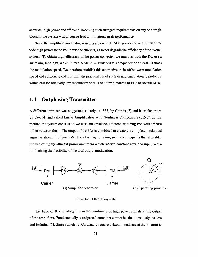
A different approach was suggested, as early as 1935, by Chireix [3] and later elaborated
by Cox [4] and called Linear Amplification with Nonlinear Components (LINC). In this
method the system consists of two constant envelope, efficient switching PAs with a phase
offset between them. The output of the PAs is combined to create the complete modulated
signal as shown in Figure 1-5. The advantage of using such a technique is that it enables
the use of highly efficient power amplifiers which receive constant envelope input, while
not limiting the flexibility of the total output modulation.
Q
$1(t) $2(t) .PM > E A+ PM .
CarrierCare(a) Simplified schematic (b) Operating principle
Figure 1-5: LINC transmitter
The bane of this topology lies in the combining of high power signals at the output
of the amplifiers. Fundamentally, a reciprocal combiner cannot be simultaneously lossless
and isolating [5]. Since switching PAs usually require a fixed impedance at their output to
21
guarantee the non-overlap of the output current and voltage waveforms, thus enabling their
high efficiency, we would like the combiner to be matched, so the operation of one PA does
not affect the other and both PAs have a constant fixed impedance at their output which
can be matched. In this case though, any energy which is not combined and transmitted
is dissipated on the fourth isolating port, and its portion is greater as the outphasing angle
increases. We therefore once again lose efficiency as we transmit symbols which have
lower power than the peak power level.
1.5 Asymmetric Multilevel Outphasing (AMO) Transmitter
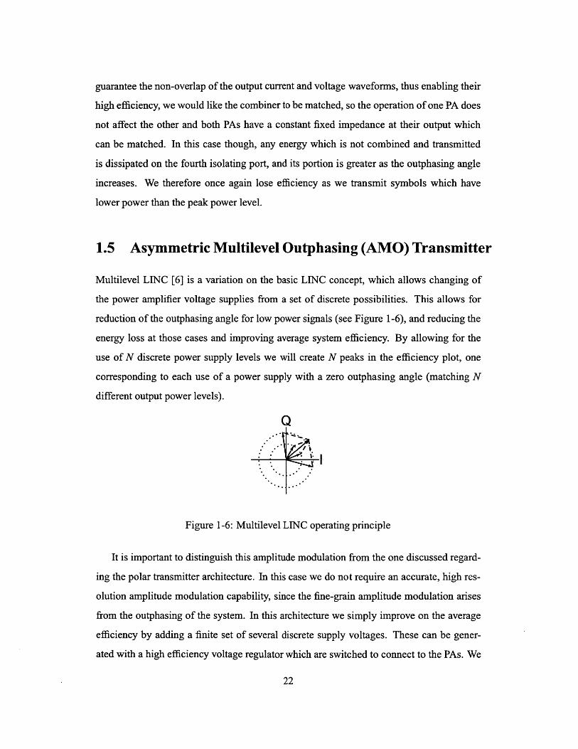
Multilevel LINC [6] is a variation on the basic LINC concept, which allows changing of
the power amplifier voltage supplies from a set of discrete possibilities. This allows for
reduction of the outphasing angle for low power signals (see Figure 1-6), and reducing the
energy loss at those cases and improving average system efficiency. By allowing for the
use of N discrete power supply levels we will create N peaks in the efficiency plot, one
corresponding to each use of a power supply with a zero outphasing angle (matching N
different output power levels).
Q
Figure 1-6: Multilevel LINC operating principle
It is important to distinguish this amplitude modulation from the one discussed regard-
ing the polar transmitter architecture. In this case we do not require an accurate, high res-
olution amplitude modulation capability, since the fine-grain amplitude modulation arises
from the outphasing of the system. In this architecture we simply improve on the average
efficiency by adding a finite set of several discrete supply voltages. These can be gener-
ated with a high efficiency voltage regulator which are switched to connect to the PAs. We
22
are therefore reducing much of the complexity required in the polar architecture by not
demanding that the amplitude modulation block have high accuracy and resolution.
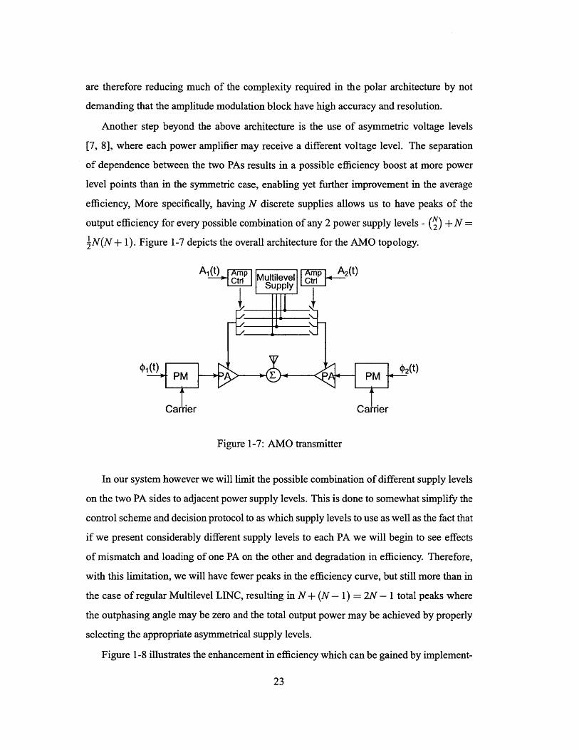
Another step beyond the above architecture is the use of asymmetric voltage levels
[7, 8], where each power amplifier may receive a different voltage level. The separation
of dependence between the two PAs results in a possible efficiency boost at more power
level points than in the symmetric case, enabling yet further improvement in the average
efficiency, More specifically, having N discrete supplies allows us to have peaks of the
output efficiency for every possible combination of any 2 power supply levels - (2) +N=
'N(N + 1). Figure 1-7 depicts the overall architecture for the AMO topology.
A1 1 Multilevel p 2(t)
01M PM PM 02t
Carrier Carrier
Figure 1-7: AMO transmitter
In our system however we will limit the possible combination of different supply levels
on the two PA sides to adjacent power supply levels. This is done to somewhat simplify the
control scheme and decision protocol to as which supply levels to use as well as the fact that
if we present considerably different supply levels to each PA we will begin to see effects
of mismatch and loading of one PA on the other and degradation in efficiency. Therefore,
with this limitation, we will have fewer peaks in the efficiency curve, but still more than in
the case of regular Multilevel LINC, resulting in N + (N - 1) = 2N - 1 total peaks where
the outphasing angle may be zero and the total output power may be achieved by properly
selecting the appropriate asymmetrical supply levels.
Figure 1-8 illustrates the enhancement in efficiency which can be gained by implement-
23

ing Multi-Level LINC and the AMO architecture compared to LINC as described above.
In this example we see the use of 4 different supply levels, which contribute to the creation
of 4 efficiency peaks in the ML-LINC case and 7 efficiency peaks for the AMO case as
predicted. The location of the efficiency peaks may be optimized by properly scaling and
setting the supply voltage levels which may be done in such a manner to correlate with
the desired communication protocol's power probability distribution, therefore placing the
efficiency peaks at the locations where the transmitter will be operating the majority of the
time thus improving the average efficiency of the overall system [7].
100
90
80
7.
AowE
70
60
50
40
30
20
-10 ---10 -8 -6 -4 -2
Normalized Output Power [dB]0
Figure 1-8: Ideal efficiency comparison between LINC, ML-LINC and AMO architectures
1.6 Research Contributions
Previous work has been done to show the benefits and potential improvement of average
efficiency with the use of the AMO architecture in cellular frequency bands [9, 10]. In this
research I will focus on the design and implementation of two of the key building blocks
of this architecture - the amplitude switching network and the phase modulator.
24

In Chapter 2 I will present the design considerations, implementation and simulation
testing of a power supply switching network for an AMO architecture operating at mm-
wave frequencies. The many challenges that arise when dealing with a high carrier fre-
quency of 45 GHz, accompanied by a very fast data rate will be discussed and analyzed
along with various concepts to allow improvement of the linearity of the overall system.
A new technique for achieving accurate and fast phase modulation required for AMO
systems will be presented in Chapter 3. A detailed analysis of the deign considerations and
theory will be presented and the results of measurements of a 65 nm test chip implementing
the new design will be discussed, showing an effective 10.2 bit resolution and a settling time
of less than 5 carrier cycles to within ±10. The phase modulator also complies with the
spectral masks for transmitting in the Medical Implant Communication Services (MICS)
band.
25

26

Chapter 2
Amplitude Modulation
2.1 Introduction
Amplitude modulation has been an integral part of communication systems since their very
earliest days as a method of transmitting data. The simple methods for modulating and
demodulating an amplitude of a signal helped spread its use in communication systems.
In the AMO architecture however it is important to understand that the amplitude mod-
ulation we are interested in differs from this traditional view of amplitude modulation. We
are not performing amplitude modulation which will directly change the transmitted sym-
bol, that will be achieved via the combining of the outphased signals. The amplitude modu-
lation is done to the PA power supply to enable high efficiency by minimizing the required
outphasing angle at different output power levels. In this sense, our amplitude modulation
resembles more a power converter rather than a traditional amplitude modulation.
It is important to understand what exactly are our requirements from the AM path.
Since we are supplying the power to the PA supply, we do require it to be high power
and therefore also efficient, since otherwise we will degrade the overall system efficiency
due to this block. We may also require this path to be fast, comparable to the sample rate
(although this demand might be relaxed a bit as we shall see later on). We do not however
impose a demand on the AM block to be accurate. Unlike the polar architecture where
the signal's amplitude modulation derives from the AM block and thus requires it to have
a high dynamic range and resolution for adequate output levels for complex modulation
27

schemes [11], the AMO architecture only requires the ability to toggle amongst a few
discrete predetermined levels.
This theme, not demanding to "have it all" will also appear later in Chapter 3 where we
discuss the requirements from the Phase Modulator (PM) block for our system. We will
see that there we will have a different set of requirements and demands, but again, we will
avoid demanding that a system be simultaneously fast, accurate, high power and efficient.
This relaxation in demands is what enables us to gain the important aspects of the circuits
and compromise on the less critical ones towards a successful overall system design.
2.2 Power Supply Switch Network
Now that we have defined the required properties of our AM block we may more precisely
define how we wish to implement and achieve these goals. In this work we will discuss
the design and simulation of the power switching network built for use in an AMO ar-
chitecture targeted for operation at mm-wave frequencies of 45 GHz. This project will be
implemented in 45 nm Silicon On Insulator (SOI) technology. The use of SOI technology
allows us to achieve higher operating frequencies for the transistors, and also opens up
some possibilities in the design of the power switches as we shall shortly see. Our design
utilizes 4 power supply levels - 1.1, 1.4, 1.8 and 2.2 Volts. This range was chosen to al-
low for flexibility in the output power while limiting the maximum supply level to twice
the nominal supply voltage, and the difference between lowest and highest supply to one
maximum nominal voltage setting.
A block diagram of the proposed power supply switch and control network is shown in
Figure 2-1. This control scheme is replicated for each PA. The 2 bit control word A,[1 : 0]
(x referring to one of the two outphasing PAs) is passed through a tunable delay element
controlled by a 6 bit control word Dx[5 : 0], it is then decoded, with a selection whether to
enforce switch control overlap or a dead-time period. The 4 individual switch control sig-
nals are level shifted before driving the actual power switches through a slew-rate controlled
driver chain. The following sections present a detailed explanation as to the importance of
each circuit in the overall block, its design considerations and simulation results.
28

VDDi
A[:]2 2 LAx[1:i Decoder 2to4 | x4 >
6 SL[2:0] VOUTx
Dx[5:0]OVLP
Figure 2-1: Power supply switching network block diagram
2.2.1 Switch Design
We shall begin our analysis from the last building block of the circuit - the power switch
itself. The last stage of the pipeline needs to relay the various power supplies to the PA
drain with minimum interruption manifesting as voltage drops and power loss. Since in
our design we are only required to toggle amongst 4 possible power supply levels which
are generated off-die, we will implement the switches as simple NMOS/PMOS devices
conducting the supplies based on their control signals. All switches will be connected to
their respective supply, and on their other side shorted together and connected to the PA
drain through a choking inductor.
Since the supplies themselves are constrained to the set VDDi E [1.1, 1.4,1.8,2.2] the
PA drain, denoted as VOUTX will also be a value in that range. This means that we can
think of the system as operating in a shifted version of a "regular" system which would
operate between ground and VDD1. We may preform this level shifting since we are using
SOI CMOS technology and the bulk node is left floating. Thus, we may use only a single
device as the switch, foregoing the need to cascade devices. We will discuss this attribute
further in Section 2.2.4
Previous work has explored the switch design considerations for lower frequencies as
for different fabrication processes [12]. One of the main design aspects of the switches is
the choice of device type (N or P) as well as the sizing of the devices. In order to help
determine the appropriate sizing, a simulation deck was constructed to mimic the operation
environment of the switches. In our architecture each PA is further separated into 8 in-
29

phase PAs in order to distribute the output power requirements over multiple blocks. The
layout of the switch blocks was done to accommodate with this topology, associating a
separate switch block with each PA slice. The simulations following were also preformed
on a single PA slice and therefore the transistor sizings correspond to one such slice.
Although from the description so far one might consider the system to be symmetrical
in respect to the various power supplies, one should keep in mind that the use of higher
power supplies correspond to a higher output power and to fewer high power symbols in
the constellation. In fact, a closer look at a typical data set, transmitting random 64-QAM
symbols oversampled by 2, reveals a very uneven distribution of use of power supplies.
Figure 2-2 shows the frequency of use of each power supply level for an example data
set consisting of 10,000 samples. As can be seen, a vast majority of almost 60% of the
samples uses the lowest power supply, an additional 25% use the second lowest, 15%
use one higher and a mere 0.7% use the highest supply level. It is important to keep
these numbers in mind when considering the importance and optimization of each part in
the system. We will choose to implement all switches having the same size, this may be
0
50-
ca40--
ECO
U)0 30-
0-a.
0
0
0.8 1 1.2 1.4 1.6 1.8 2 2.2 2.4 2.6Supply Level [V]
Figure 2-2: Supply level usage histogram
30

considered sub-optimal due to the inherent differences between NMOS and PMOS devices,
but as we shall see further on, these differences are small and the advantages of simple and
reusable patterned layout exceed them. We will also choose to implement the switches for
the bottom two supples as completely NMOS, and the switches to the top two supplies as
completely PMOS. Here the choice is a matter of preferring simple reusable layout, as well
as a more simplified control scheme over pin-point optimization which is not very sensitive
to these changes as we shall shortly see.
The two main sources of inefficiency and power loss in a switch are conductive losses
and switching losses. Conduction loss can be accounted for by the fact that the non-ideal
switch has a finite on-resistance, which therefore causes a voltage drop to form across its
terminals while it is conducting current, and this loss resembles ohmic conductive losses
and can be represented as
Pcond = VDSIDS (2.1)
In a MOS transistor, the equivalent resistance is inversely proportional to the devices width,
so we can expect that the conduction loss (as well as the voltage drop across the switch)
will go down as the device size increases, and this is shown in the simulation result plotted
in Figure 2-3 for the NMOS and PMOS switches.
Switching losses arise due to the fact that in order to open and close the switch we
must charge and discharge capacitive loads, namely the transistor's gate capacitance. The
moving of charge back and forth, even through small source resistances accounts for power
dissipation. The amount of charge required to charge or discharge a capacitive load C by a
voltage difference AV is given by
AQ = CAV (2.2)
If we now assume that the switch is opened and closed regularly with a clock frequency f,and an activity factor a, representing how often the switch is typically opened and closed,
e.g. opening and closing it alternatively every clock cycle will result in a maximum activity
factor of a =j. We may define an effective switching current
Isw = 4 = aCAVf (2.3)at AT T
31

50-- NMOS
45- --- PMOS
40-
35 -E
30-
-j 25-0
20-
00 15-
10-
00 1 2 3 4 5 6
Width [mm]
Figure 2-3: Switch conduction losses
So the switching power loss can be defined as this switching current times the voltage
difference used to charge and discharge the load capacitance
Ps, = IWAV = caCAV 2f (2.4)
The maximum desirable clock frequency, or sample rate, in our system is f = 4GHz.
The voltage difference as discussed above is in our case AV = 1.1 V. The activity factor
may vary, and in the worst case is equal to half, but a more realistic value examining sample
data sets suggests a typical value would be closer to a = 1. This is also reinforced by the
results shown in Figure 2-2, since if we are 60% of the time at the lowest supply level it
is not possible that we would switch each and every clock cycle. The load capacitance
is basically the switch total gate capacitance which we require to charge and discharge
in order to open and close the switch for conduction. The gate capacitance is linearly
proportional to the device width and therefore increases with the scaling of the transistor
size as shown in Figure 2-4. We can see that for the NMOS devices the gate capacitance is
32
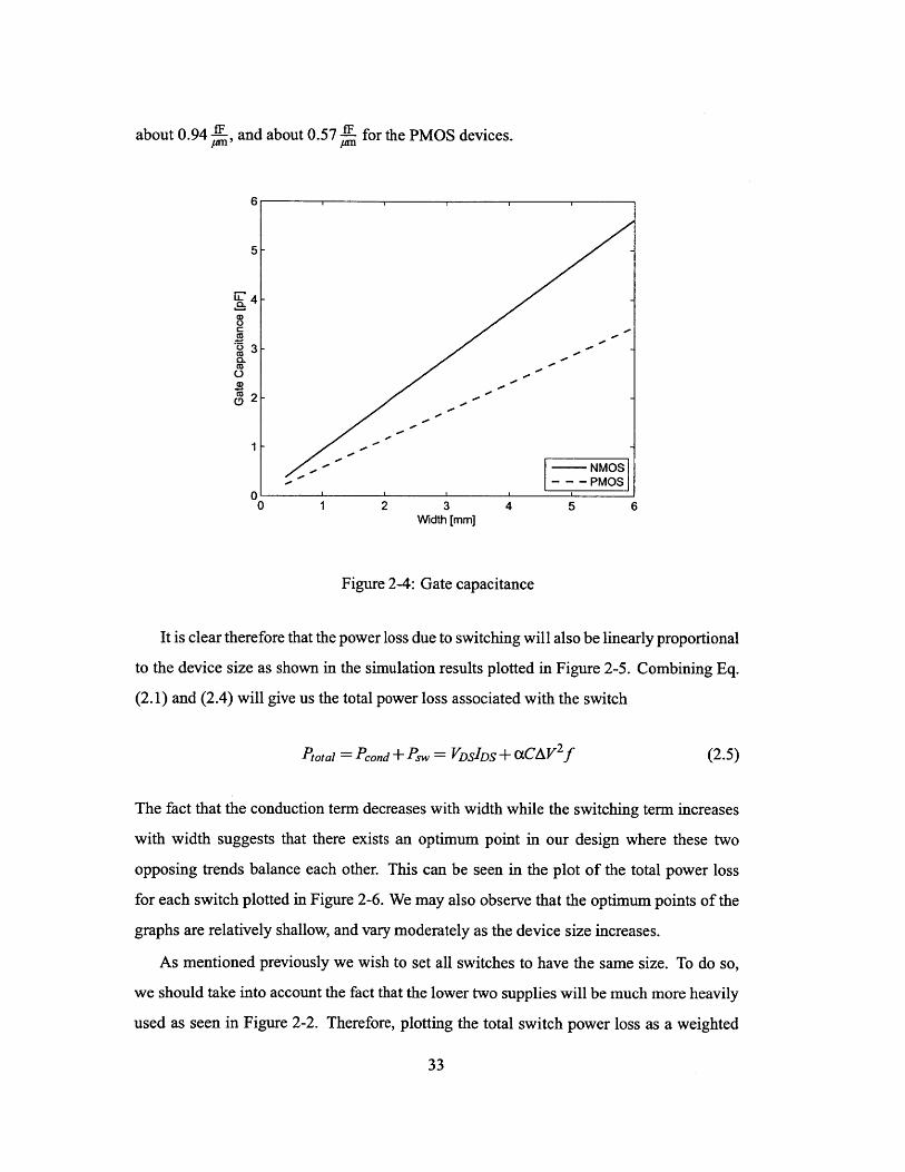
about 0.94 -, and about 0.57 for the PMOS devices.
3C 4 -.-
C 3
NMOS-- PMOS
00 1 2 3 4 5 6
Width [mm]
Figure 2-4: Gate capacitance
It is clear therefore that the power loss due to switching will also be linearly proportional
to the device size as shown in the simulation results plotted in Figure 2-5. Combining Eq.
(2.1) and (2.4) will give us the total power loss associated with the switch
Ptotal = Pcond+P = VDSIDS + aCAV2f (2.5)
The fact that the conduction term decreases with width while the switching term increases
with width suggests that there exists an optimum point in our design where these two
opposing trends balance each other. This can be seen in the plot of the total power loss
for each switch plotted in Figure 2-6. We may also observe that the optimum points of the
graphs are relatively shallow, and vary moderately as the device size increases.
As mentioned previously we wish to set all switches to have the same size. To do so,
we should take into account the fact that the lower two supplies will be much more heavily
used as seen in Figure 2-2. Therefore, plotting the total switch power loss as a weighted
33

7
E
0
CO
0 1 2 3 4 5 6Width [mm]
Figure 2-5: Switch switching losses
63Width [mm]
Figure 2-6: Switch total power loss
34
50
45
40
§735E0n 300D0
-J 25
020
15
10
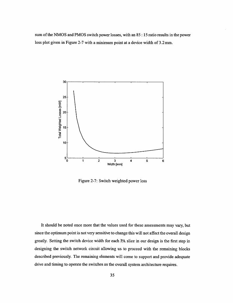
sum of the NMOS and PMOS switch power losses, with an 85: 15 ratio results in the power
loss plot given in Figure 2-7 with a minimum point at a device width of 3.2 mm.
30
25-
E
20-0
15-
0)
10- -
5 '0 1 2 3 4 5 6
Width [mm]
Figure 2-7: Switch weighted power loss
It should be noted once more that the values used for these assessments may vary, but
since the optimum point is not very sensitive to change this will not affect the overall design
greatly. Setting the switch device width for each PA slice in our design is the first step in
designing the switch network circuit allowing us to proceed with the remaining blocks
described previously. The remaining elements will come to support and provide adequate
drive and timing to operate the switches as the overall system architecture requires.
35

2.2.2 Time Alignment
One of the most important aspects of the AMO system which must be taken into consid-
eration is the time alignment between the signals of the two combining PAs, as well as the
time alignment between the amplitude path and phase path for each PA on its own. The
first aspect exists only in outphasing systems, while the second is true to all transmitter
architectures, but is more pronounced in systems which employ a polar-style modulation.
For linear transmitters using I and Q data paths, there is an inherent symmetry between the
two signal routes, so symmetrical, matched layout may help greatly to reduce offsets and
mismatches and align the signals. When the signal is broken down to amplitude and phase,
it suffers from the fact that these two components will most likely transverse very different
paths to the output, so one cannot guarantee matching and alignment by design and layout.
In this case intentional, implicit time alignment blocks are necessary to make sure that each
symbol arrives properly to the transmitter and that the two sides are working in unison.
To allow for such time alignment between paths, and between sides, we shall introduce
into the system a controlled delay element in each of the paths (amplitude and phase) in
order to allow skewing of the signal arrival time in any direction. It should be noted that
it will probably be an easier task to delay and time align not the actual signals themselves
after modulation, but rather the coded control signals which arrive to the individual blocks,
due to their digital nature and high Signal to Noise Ratio (SNR).
We will require a control range which can span up to half of a sample period to allow
complete coverage. If the mismatch between two paths is greater than half a sample period
we may correct this simply by delaying the digital input by the required sample amount
to reduce the mismatch to within half a sample period. It would seem this constraint will
impose a minimum data rate frequency which we can operate in, however, for lower data
rates with longer sample times, the relative offset between the paths becomes less signifi-
cant since it is a much smaller fraction of the sample period.
To achieve the ability to delay the control signals by time periods which are smaller
than the sample period implies we will not be able to do so in a digital manner, which
will require a much faster clock signal to do so. Therefore we will employ an absolute
36
delay scheme, though it will indeed have the drawback that it does not scale with the clock
frequency, but as mentioned previously, the absolute delay becomes less meaningful as the
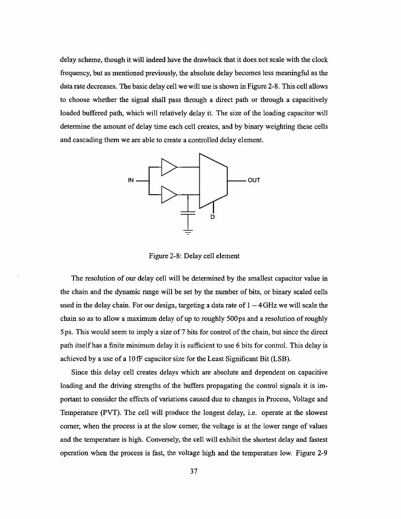
data rate decreases. The basic delay cell we will use is shown in Figure 2-8. This cell allows
to choose whether the signal shall pass through a direct path or through a capacitively
loaded buffered path, which will relatively delay it. The size of the loading capacitor will
determine the amount of delay time each cell creates, and by binary weighting these cells
and cascading them we are able to create a controlled delay element.
IN OUT
>T
Figure 2-8: Delay cell element
The resolution of our delay cell will be determined by the smallest capacitor value in
the chain and the dynamic range will be set by the number of bits, or binary scaled cells
used in the delay chain. For our design, targeting a data rate of 1 - 4GHz we will scale the
chain so as to allow a maximum delay of up to roughly 500ps and a resolution of roughly
5ps. This would seem to imply a size of 7 bits for control of the chain, but since the direct
path itself has a finite minimum delay it is sufficient to use 6 bits for control. This delay is
achieved by a use of a 10 fF capacitor size for the Least Significant Bit (LSB).
Since this delay cell creates delays which are absolute and dependent on capacitive
loading and the driving strengths of the buffers propagating the control signals it is im-
portant to consider the effects of variations caused due to changes in Process, Voltage and
Temperature (PVT). The cell will produce the longest delay, i.e. operate at the slowest
corner, when the process is at the slow comer, the voltage is at the lower range of values
and the temperature is high. Conversely, the cell will exhibit the shortest delay and fastest
operation when the process is fast, the voltage high and the temperature low. Figure 2-9
37

illustrates this via a corner simulation of a code sweep of the delay cell, measuring the
delay of a test signal propagating through. The nominal values were taken to be at 27 C
and a supply voltage of 1 V. The slow corner was simulated with the temperature at 1000 C
and VDD = 0.9V and the fast corner was set at 0 C and a supply voltage of 1.1 V.
600- -
500 -
400
00
200-
- - - Slow
100 -Nominal------- Fast
0 10 20 30 40 50 60Delay Code
Figure 2-9: PVT corner simulation of delay cell
2.2.2.1 Nulling Test
An extremely important aspect (albeit sometimes overlooked) of being able to control, trim
and program various components and blocks in a system is the ability to test it and de-
vise a scheme to enable the proper setting of the component. An extensive and flexible
programmable device is still worthless if one cannot define a way to determine how it
should be set. In our system, as described earlier, there are two main time alignments to
be concerned with - time alignment between the phase and amplitude paths and alignment
between the two outphasing PAs. Our chosen architecture of Asymmetric Multilevel Out-
phasing opens up the possibility to determine the correct timing alignment in interesting
ways.
38

For both cases we will employ a similar concept - "Nulling" tests, i.e. experiments
where the outcome should be null, or have minimal effect. This can be achieved in general
in a system which is non-injective, so as to have two or more states which will yield the
same outcome. In our case, to determine the proper timing between the two outphasing
PAs we may subject a test where the amplitude is initially set different for the two sides,
than simultaneously swap, so
al (t2) = a2(ti) and a2(t2) = al (ti) where a (ti) # a2(tl) (2.6)
Due to the symmetry of the system the output should ideally remain unchanged, there-
fore any misalignment of the timing paths between the two sides will pronounce itself via
perturbations to the combined output resulting in a momentary change in amplitude or a
degradation of the noise floor of the output spectrum. An example of this is shown in Fig-
ure 2-10. This will determine the relative timing offset between the two outphasing sides.
0.2 0.3 0.4 0Time [ns]
.5 0.6 0.7 0.8
Figure 2-10: Amplitude path misalignment of 100ps
39
4
3
2
1
0
0,
CD
-1
-2
-3
-4 t0.1

Similarly, due to the fact that our system employs several levels of possible supply
voltages there is more than one set of phase and amplitude which will yield a given output.
This fact enabled us to switch to a lower amplitude with a smaller outphasing angle in order
to improve average efficiency and it will also enable us to determine the timing alignment
between the phase and amplitude paths. Again we set an experiment where now, after the
two sides are aligned, we switch the amplitude and phase values while still ideally obtaining
the same output value. Any misalignment will again manifest itself in a disturbance of the
amplitude and phase of the combined output waveform.
In both alignment cases we may not be able to achieve an ideal result, but this scheme
does provide a way to achieve the best result by minimizing the output disturbance and the
signal spectrum's noise floor.
2.2.3 Decoding and Overlap Control
The control signals arriving to the switches are sent binary coded and therefore need to be
decoded before the actual commands are passed through to open and close the appropriate
switches. The decoding process is straight forward, and done via a simple digital 2-to-4
decoder as shown in Figure 2-11. At each given time point only one switch control signal
should be high, corresponding to the desired PA supply voltage.
A[1] A[O]
Cti[O]
Ctr1[1]
ctrI[2]
ctr1[3]
Figure 2-11: 2-to-4 Decoder
Special attention should be given to the transition between any two supply levels, i.e.
the switch control transition hand-off from one control to the other. Ideally this transition
40

would occur instantly, where one control goes down in zero time, the other goes up si-
multaneously in zero time. Of course, this is not a realistic model of the control signals.
The drivers have finite rise and fall times therefore we are guaranteed to have either an
overlap between two signals during transition, or a dead-time where no switch is on. An
overlap between the signals will cause a short period of time where two supplies are ba-
sically shorted together, and so a shunting current will flow from one to the other through
the switches causing power losses and efficiency degradation. On the other hand, a dead
time, will cause an intermittent droop in the voltage supplied to the PA degrading the sym-
bol output and spectrum. The amount of power loss or voltage drop is dependent on the
transition time, the switch resistances and the capacitance on the supply node.
In order to allow for maximum system flexibility and allow for different trade-offs in
the digital pre-distortion block, a mechanism was introduced to ensure either a guaranteed
short overlap of control signals or a guaranteed non-overlap. This is achieved using the
simple circuit depicted in Figure 2-12(a). The AND gate with the delayed input ensures
that the output will have a delayed rise compared to its input, this is suited to the case
where we wish there to be no overlap, if we invert the polarity of the signal before and
after the delayed AND buffer it will effectively result in a signal with a delayed falling
edge, which is suitable for use in the case where we do desire an overlap. The inversion of
polarity is easily achieved by the XOR gates at the input and output, where the other leg is
connected to a signal indicating the desired state (low for no overlap and high for overlap).
An illustration of the signal timings is presented in Figure 2-12(b).
Ctrl[ij] _ [ ~ ~ -1C t r L o V [ i ] O V i j]-
Lizi1 iz..V CtrI OV[i,j] EZZLE J ---i-(a) Schematic (b) Timing diagram
Figure 2-12: Overlap control scheme
As before it is crucial to verify that the desired behavior of our block remains consistent
across variations in PVT. Therefore a comprehensive sweep was preformed in simulation
to measure the amount of overlap (as a positive time value) or non-overlap (as a negative
41

time value) as a function of every possible transition between two power supply levels
and across several PVT conditions. The results shown in Figure 2-13 demonstrate that
the design assures us that the block will function as expected under all of these various
scenarios.
2.2.4 Level Shifting
As discussed earlier, the choice to use thin gate FETs enables us to operate at higher speeds
but poses severe limitations on the voltage which can be sustained across the device's ter-
minals. This limitation is even more pronounced in our deep sub-micron process where the
voltage across any 2 terminals should not exceed roughly 1.1 V. The use of SOI technology
though, removes this concern regarding the bulk node, so unlike Bulk CMOS we can use
the devices between higher voltages, so long as the difference between any two terminals
is less than the maximum allowed and we are not constrained to have all bulk nodes tied to
one common voltage level. Therefore we may use the switch devices between the power
supplies and the PA drain without the need to cascode it as long as we keep the difference
between the maximum supply to the lowest one to be below 1.1 V, as it is in our case.
This operating scheme requires however that we use some sort of level shifting for
the switch control signals in order to provide adequate over-drive to the transistors. In
our design, since the supplies and PA drain will always vary between VDD1 = 1.1 V and
VDD4 = 2.2V we may obtain proper overdrive of the switches by transitioning the driver
signal from their usual domain between ground and VDDI to a shifted domain between VDD1
and VDD4. This is achieved via a level shifter topology [13] shown in Figure 2-14. In this
topology the bottom inverters and the input operate at the lower voltage domain, between
ground and VDD1, the top inverters operate at the higher voltages and the cascoding middle
devices ensure the separation between the two domains and relieve the stress on the devices
when transitioning from one domain to the other.
For simplicity, let us define the ground voltage as '0', the lowest supply as '1' and the
maximum supply as '2', such that we require that each device has a differential voltage no
greater than '1' across its various terminals. We may understand the operation of this level
42

-15
EI-0.Co
a)
0
Transition
(a) Without overlap
*L 35
30-
>25-0.
20 - -
15-Slow
10- Nominal -- ..- Fast
5'0-->10-->20-->31 -- >01-->21-->32-->02-->12-->33-->03-->13-->2
Transition
(b) With overlap
Figure 2-13: Overlap time vs. transition and PVT (negative time indicates dead-time)
43

out
'1'
'2' '1'
MPO
'2'MnO
in'0'
M
Mn1
out
'2'
'1' '2'
MPo
'0'Mao
M1
'2'Mn1
in
(a) Input low (b) Input high
Figure 2-14: Level shifter schematic
shifter by following the signal change path from input to output. For a signal at the input
which goes from a low '0', to a high '1', the bottom inverter outputs change accordingly.
The bottom NMOS transistors (Mo and Mni) begin conducting. Mno starts discharging
the middle node bringing it to '0', MnI begins charging the middle node to '1' (although it
will do so only up until a threshold voltage below that). At this point only the left hand
side PMOS, Mpo will be open and begin discharging the left node. Since Mpi is closed,
the discharging may overcome the back-to-back inverter "memory" and flip its state, at
that point Mp1 will open and charge the right middle node to '2' and the output buffer will
propagate the change in the output from '1' to '2' and the transition is complete.
Similarly, going from a high '1' to low '0' at the input will first open the two bottom
NMOS devices, but this time it will charge the left middle node and discharge the right
middle node. At this point the open right PMOS, Mp1 will allow the discharge of the right
half of the inverter loop, causing them to flip and change the output from a high '2' to a low
'1'. Again ensuring throughout the entire procedure that no device encounters a differential
voltage greater than one supply level between any of its terminals.
44

2.2.5 Slew Rate Control
The driver stage preceding the power switches are responsible for providing adequate drive
strength in order to open and close the switches at a reasonable rate. In this section we will
review how varying the driver strength affects the switch and output rise and fall times and
how this may serve us in the overall system output shaping.
To analyze the effects of varying rise time of the output supply amplitude, we will
make a few simplifying assumptions. Let us consider a scenario (which is actually very
pessimistic according to our discussion so far) that we wish to toggle the output between
the lowest and highest supply at the maximum data rate. In this case, the output will take
the form of a periodic square wave function, which we can normalize to a magnitude of 1,
with pulses of width ts, the data rate, and period T = 2ts. This waveform can be expressed
as
1 t< 'tsf(t) = (2.7)
0 else
Where also
f(t+nT)=f(t) VnEZ (2.8)
For this waveform, the corresponding frequency domain Fourier series is
F(on) = tssinc tson
ts n = 0
= tssinc n = { 0 n even (2.9)
(-1)n+1 n odd
The finite rise time of the output square wave may be modeled as a linear slope. This is
of course not accurate, but close and will allow us to conduct rough simplified calculations
and analysis. The finite rise time tr, can be generated in our waveform as a convolution of
the original ideal square wave with an additional periodical square wave with width tr and
45
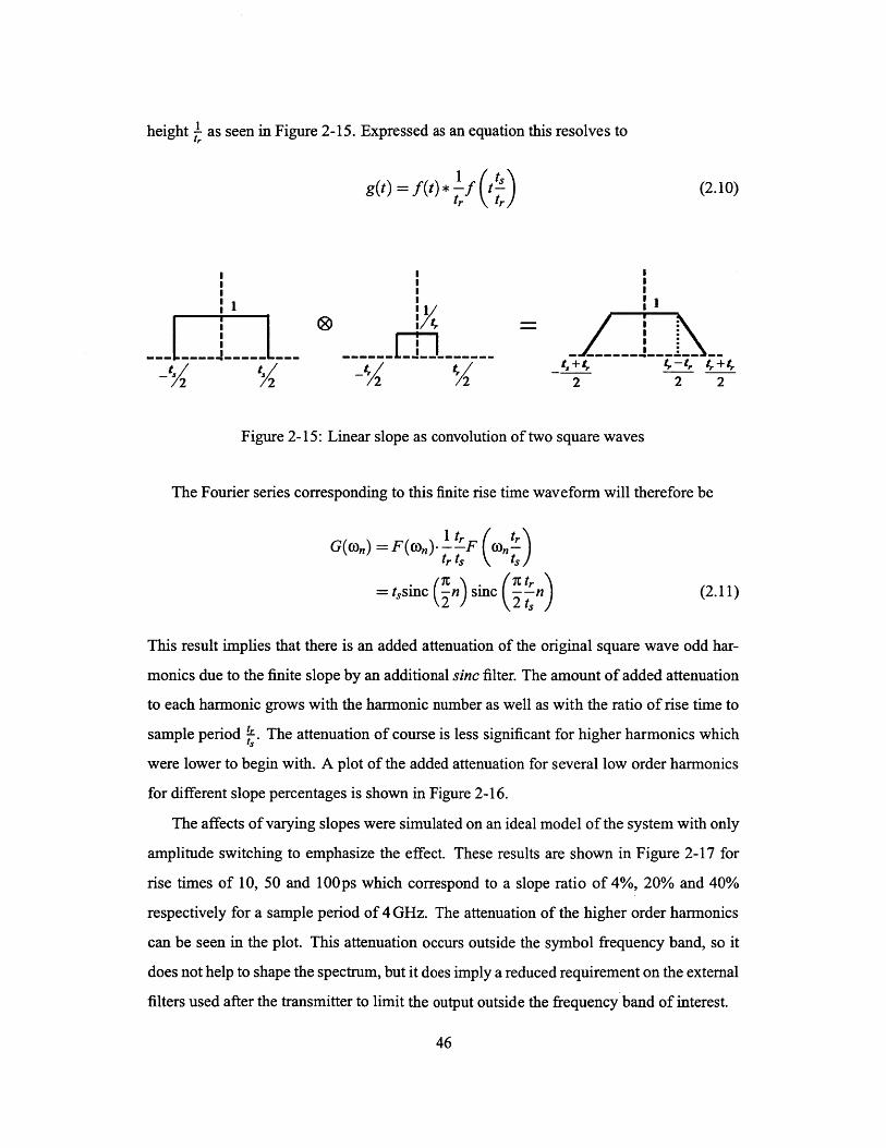
height -as seen in Figure 2-15. Expressed as an equation this resolves to
g(t) = f(t)* -f t (2.10)tr \tr/
-2 /2 2 2
Figure 2-15: Linear slope as convolution of two square waves
The Fourier series corresponding to this finite rise time waveform will therefore be
1 tr (trG(con)= F((on) - I rF con-ttr ts ts
= tssme -Cn smec --trn (2.11)(2 ) 2 ts
This result implies that there is an added attenuation of the original square wave odd har-
monics due to the finite slope by an additional sinc filter. The amount of added attenuation
to each harmonic grows with the harmonic number as well as with the ratio of rise time to
sample period -. The attenuation of course is less significant for higher harmonics which
were lower to begin with. A plot of the added attenuation for several low order harmonics
for different slope percentages is shown in Figure 2-16.
The affects of varying slopes were simulated on an ideal model of the system with only
amplitude switching to emphasize the effect. These results are shown in Figure 2-17 for
rise times of 10, 50 and 100ps which correspond to a slope ratio of 4%, 20% and 40%
respectively for a sample period of 4GHz. The attenuation of the higher order harmonics
can be seen in the plot. This attenuation occurs outside the symbol frequency band, so it
does not help to shape the spectrum, but it does imply a reduced requirement on the external
filters used after the transmitter to limit the output outside the frequency band of interest.
46

0.2 0.4 0.6Slope Ratio [tr/t,]
0.8 1
Figure 2-16: Added attenuation due to varying slopes
30 35 40 45 50 55 60Frequency [GHz]
Figure 2-17: Output spectrum for various rise times
47
40
35
30
25
20
15
10
5
0
C
---- n=1
--n=5
- -
- -'
- -'
- -
- -
n'0
0
M
-
0cI

In order to achieve this possible control over the switch slope, the driver stage was
designed as a tri-state buffer where the number of active scaled buffers could be controlled.
This does not give very accurate control over the output slope but does allow for some
flexibility in the choice of the final slope rise time. Figure 2-18 plots the simulated rise
time of the switch output given the different 3-bit control word.
An artifact of the increased rise time is also an increase in absolute delay of the circuit
from the moment the control word changes until the output is modified as shown in Figure
2-19. However this delay is relatively fixed and can be canceled out using the same tech-
niques described in Section 2.2.2 once the desired slope is selected for use in the system.
Figure 2-18 also reveals that the lowest code values create rise times which are in a
time scale larger than our maximum designed data rate, meaning that they are impractical
to use for the extreme speed case. There is however still merit in using them when going
to lower data rates, or for an alternative slewing scheme where we intentionally set the am-
plitude switching to be slower than a sample period. In such a scenario, we may relax the
requirements on the power switching network such that it is not required to toggle at the full
sample rate, but perhaps change in a more relaxed rate, say every 5 or 10 sample periods.
This relaxation will greatly reduce requirements on the block and its power consumption.
We do however require in this case to compensate for the degraded control of amplitude
by our still fast control of the phase. As long as the transitions from one amplitude level
to another are systematic and predictable, we can compensate for the inaccurate amplitude
transition time by correctly pre-defining a correction to the phase values during such tran-
sitions. These corrections require of course more digital-intense background calculation
and lookup tables but may still be worth the effort given the relaxed demands on the high
power switches.
48

0.81
e 0.6-E
a)
0.4-
0.2-
0'0 1 2 3 4 5 6 7
Code
(a)
90
80
70-
60-a.
50-i-a)
i 40-
30-
20-
103 3.5 4 4.5 5 5.5 6 6.5 7
Code
(b)
Figure 2-18: (a) Output slope rise time and (b) zoom-in
49

'- 0 0.8-
0 0.6 -
0.4-
0.2-
0'0 1 2 3 4 5 6 7
Code
Figure 2-19: Static delay caused by slew rate control
2.3 Summary
The design and analysis of a power switching network for an Asymmetric Multilevel Out-
phasing transmitter was presented. The power switching network was designed to toggle at
a maximum sample rate of 4 GS/s between 4 discrete power supplies to provide sufficient
current to the outphasing PAs. Use of the SOI process technology enabled to use level shift-
ing to reduce the number of devices and increase circuit speed without neglecting reliability
and breakdown considerations. The switch control scheme was planned with a high degree
of flexibility allowing to control overlap of control signals and their timing for alignment
between the different amplitude and phase paths, as well as output slew rate in order to
allow more degrees of freedom in the system to trade off performance and efficiency.
The proposed design was implemented and fabricated in an IBM 45nm SOI process,
as part of a complete AMO transmitter architecture. The test chip is currently back in the
lab for testing and measurement results should follow in the coming months to demonstrate
many of the aspects discussed in this work.
50

Chapter 3
Phase Modulation
3.1 Introduction
When considering the requirements of the Phase Modulator (PM) block for an outphasing
system, we can note several key features which are of interest and define our system
The PM needs to be very fast. We require that the phase output will settle quickly to
enable a high change rate required to achieve a high data rate and enable oversampling if
desired. Furthermore, as mentioned in Section 2.2.5 it is desirable to have a fast PM to be
able to compensate for a lack of speed in the amplitude path.
The PM must have a high accuracy, or resolution. Unlike other communication systems
where the phase offset block requirements are usually modest, calling for a phase offset of
900 or at most 450, in an outphasing system we need a phase resolution capable of at least
creating all the desired symbols we wish to generate, and it will likely need to be of much
higher resolution in order to enable oversampling and compensation for the amplitude path.
Fortunately, the PM block does not need to be high power, and as a consequence does
not need to have high efficiency either. The block does not provide the power to the PAs
(unlike the voltage regulator in the EER topology), and thus gives us some leeway in our
design.
There exists a myriad of ways to create a desired phase shift in a signal. Some of these
include tapped delay lines, where the signal is passed through varying delays in order to
accrue the desired phase [14]. Others employ passive reactive devices to create a phase
51
shift or coupled transmission lines with reflective loads [15], or by active means, such as
an all-pass amplifier [16]. Another option is to use a tapped ring oscillator [17], which is a
convenient way to merge the frequency generation function with a delay line.
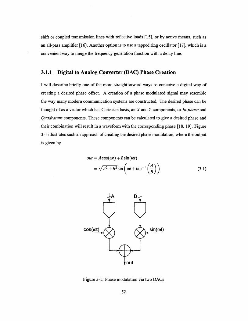
3.1.1 Digital to Analog Converter (DAC) Phase Creation
I will describe briefly one of the more straightforward ways to conceive a digital way of
creating a desired phase offset. A creation of a phase modulated signal may resemble
the way many modem communication systems are constructed. The desired phase can be
thought of as a vector which has Cartesian basis, an X and Y components, or In-phase and
Quadrature components. These components can be calculated to give a desired phase and
their combination will result in a waveform with the corresponding phase [18, 19]. Figure
3-1 illustrates such an approach of creating the desired phase modulation, where the output
is given by
out = A cos(ot) +B sin(wt)
= /A2+B2sin ot+tan- ( (3.1)
FoPt) sinot)
"out
Figure 3-1: Phase modulation via two DACs
52

The specific behavior of the output signal's phase (as well as amplitude) will be gov-
erned by the relationship between the two command words B and A. For example, assuming
a relationship of B = v1 -A2 will yield an output waveform which has a constant ampli-
tude for any choice of control word A, but the phase will vary in a non-linear way. Another
relation which might be considered is B = 1 - A, which will yield a varying amplitude of
3 dB and a phase which is arctangent in nature, and thus non-linear but only slightly. Yet
another possibility includes, the somewhat odd at first sight, B = A which will result
in a perfectly linear phase change with A, but a very large variation in the output amplitude.
The overall relationship between control words A and B is shown for the above three
examples in figure 3-2. Also, the change in amplitude vs. the control word A, as well as
the change in phase is illustrated in Figures 3-3 and 3-4 respectively.
0 0.2 0.4 0.6 0.8 1A
Figure 3-2: DAC PM control option examples
Ideally of course, the values feeding each DAC should correspond to A = sine and
B = cos 0, where e is proportional to our input code word. This will result in a constant
amplitude level and linearly varying phase. It will also of course require the calculation
of the appropriate value for each code word, though simple approximations may also be
53
III

0.2 0.4 0.6 0.8A
Figure 3-3: DAC PM amplitude variation
0 0.2 0.4 0.6 0.8A
Figure 3-4: DAC PM phase variation
54
1
0.8-
0.6-
0.4-
0.2-
E0
E
, .-
. .. - -
B = sqrt(1-A )-.-- -B = I-A-.-..-..-. B = A/tg(7/2*A)
0 1
90
-P(,En,
I
[1 I

employed [20].
It should be noted that we are more concerned with the behavior of the phase of the
output signal, rather than the amplitude behavior. This is strengthened by the fact that the
phase modulated signal will eventually act as an input to a switching amplifier, which is
fairly insensitive to variation in the input signal's amplitude. This unwanted effect can
be further reduced by placing several stages of a limiting pre-driver between the PM and
switching power amplifier to squelch any variability in the modulated signal's envelope.
This approach to creating phase modulated signals, however robust and flexible, is very
inefficient, requiring two highly accurate and fast DACs as well as possible complex calcu-
lations of control word B based on A.
3.1.2 Current Steering DAC
An improvement on the previous concept may be obtained by replacing the two indepen-
dent DACs with a single current steering DAC [21]. The current steering DAC consists of
a set of binary weighted current sources each connecting to two branches via complemen-
tary switches. Thus, we are guaranteed that the current on one branch will be proportional
to our code word - A, and the current on the other branch will inherently be set to the
complementary value, i.e. B = 1 -A.
We have already seen previously that such a selection results in a reasonable compro-
mise, allowing the output amplitude to vary by a maximum of 3 dB, and the phase response
follows an arctangent curve fairly close to a linear characteristic, and this is easily corrected
via digital pre-distortion with the aid of a static lookup table with only a slight loss in accu-
racy. Such a system reduces much of the complexity and unneeded flexibility of the general
two-DAC configuration and allows us to achieve a scalable solution for implementing phase
modulation in our system.
3.2 Low-Q Resonant Tank Phase Modulator
If the previous phase generation method may be viewed as a somewhat "digital" approach,
we now consider a different concept which can accordingly be viewed as an "analog", or
55

"mixed-signal" approach. It takes advantage of the properties of resonant circuits for phase
shifting [22].
Let us consider the complex impedance of a parallel RLC tank (shown in Figure 3-5),
which can easily be calculated as
ZRLC =R \| joL |jo)C
W+ jo)C+jOL
R c~;tan-1(R(coC--L)) 3g
l+R2 (C- I2 2
Connecting this circuit as a load to a common source amplifier, as seen in Figure 3-6,
L R C
ZRLC
Figure 3-5: Parallel RLC tank
and providing a DC bias level through the inductor, applying a sinusoidal input signal
results in the output signal vost = -gmZRLcvin, where g,, is the transistor's small signal
transconductance. Therefore the output signal will have a phase offset in relation to the
input carrier, which can be seen from Eq. (3.2) as
A tcn= tan-o v R su oC - (3.3)
Allowing to change the capacitor value, such that it varies between a minimum value
56

Vout
Vin
^V L R 7- C
Vbias - --
Figure 3-6: Phase modulator resonant tank concept
Cmin and a maximum value Cmax, and the center value, denoted Co, is set as to tune the tank
to a desired carrier frequency o, such that
__ 1Oe = V(3.4)
We may now rewrite Eq. (3.3) for a varying capacitance while fixing the frequency to the
resonant value of the tank
Z ( vo -tan- 1 -meRQo C
Vin /Co
= tan- (Qo( - 1 (3.5)
Where we also defined the tank's quality factor at the carrier frequency and when the ca-
pacitor is set to it's median value
Qo = cocRCo (3.6)
From Eq. (3.5) we can derive another key aspect of this system. To the first order, the
effects of the different components on the output phase function are independent. Varying
the fixed capacitance of the tank, so as to set the median varying capacitor value (corre-
sponding to the middle code word in a single quadrant) to Co will ensure that the output
phase function is (anti-)symmetric, regardless of the resistor value. More so, changing the
57

resistor value will change the effective quality factor, thus for a given capacitor range will
change the phase coverage of a single quadrant, allowing us to stretch it beyond 90*, or
shrink it below it. These properties allow us to adopt an approach of "Divide and Conquer"
when coming to set the values of the different components or allow for possible trimming,
since the calibration and setting of the values can be done in an algorithmic manner which
is not inter-dependable between variables.
Consider setting the capacitor edge values to be
Cmin = C0 (I1
Cmax = CO (1+ -)
(3.7)
(3.8)
This will translate to a phase coverage of 90*, the absolute value of the capacitance required
to vary in order to obtain this coverage will depend on the quality factor. The larger it is,
the sharper the change in frequency, and the less change required in the capacitor value.
Figure 3-7 illustrates this for several quality factor values.
-5;Is
ca,
50
40
30
20
10
0
-10
-20
-30
-40
-500 0.5 1
Capacitor Value [C)
1.5 2
Figure 3-7: Phase coverage at different quality factors
58
- Q =1- - ..- Q=1.5 -
.- - - Q=2
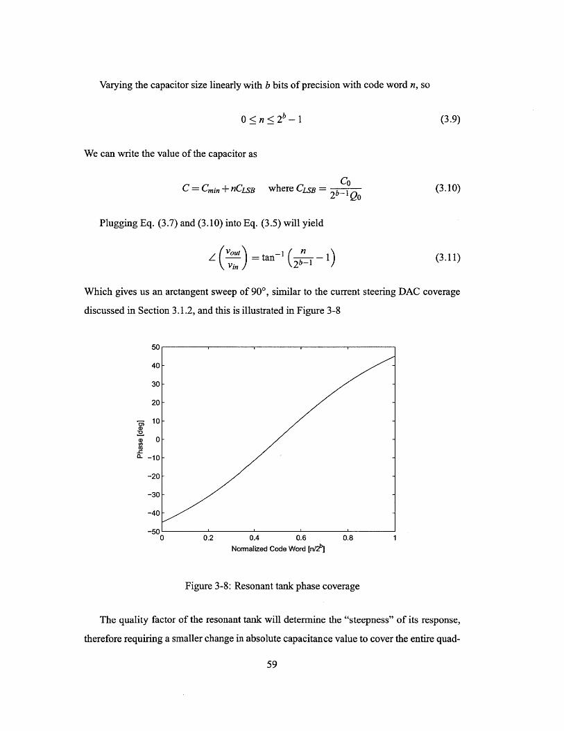
Varying the capacitor size linearly with b bits of precision with code word n, so
0 <n < - 1 (3.9)
We can write the value of the capacitor as
C0C = Cmin +nCLSB where CLSB = 2b-1 0 0 (3.10)
Plugging Eq. (3.7) and (3.10) into Eq. (3.5) will yield
-tan- ( n(-Vi nJ 21,-I(3.11)
Which gives us an arctangent sweep of 900, similar to the current steering DAC coverage
discussed in Section 3.1.2, and this is illustrated in Figure 3-8
a-
a_
50 -
40-
30-
20-
10-
0-
-10-
-20-
-30-
-40
-50 -0 0.2 0.4 0.6 0.8
Normalized Code Word [n/21'
Figure 3-8: Resonant tank phase coverage
The quality factor of the resonant tank will determine the "steepness" of its response,
therefore requiring a smaller change in absolute capacitance value to cover the entire quad-
59
1

rant. For our purposes there is no need for high frequency selectivity, therefore we may
use a relatively low quality factor value, thus the given name for our phase modulation
technique - Low-Q Resonant Tank Phase Modulator.
Given that our system is a second order system, it is a simple matter to estimate its set-
tling time given the capacitance change of the tank. The system response will be dominated
by its attenuation and damping factors, and specifically for the parallel RLC tank we are
discussing the settling time constant will be
t =2RC (3.12)
Therefore, we can estimate that the worst case time required to settle, for example, to
within 10 of the desired phase (corresponding to 0.3% of the full range) will occur for the
maximum capacitance value and will require a period of roughly
ts,0.3% 6Omax
= 12RCmax
1 -ocRCO 1+ -
~ 2(1 + Qo)Tc (3.13)
Where we used Eq. (3.6) and (3.8) for appropriate substitutions, as well as the fact that
oc = . Recalling that our system requires a rather low quality factor for its operation
yields that the settling time will be quite fast, no more than a few carrier cycles.
In order to demonstrate the properties described above, a test chip was fabricated in
65nm CMOS which implements this design (Figure 3-9). Below is a detailed explanation
of the design process and considerations involved as well as test measurement results.
3.2.1 Design Process
In order to derive the required values for the various components we will begin the design
with a choice of center frequency, which we shall set at 2.4 GHz to enable operation at the
60

Figure 3-9: Chip micrograph
Industrial, Scientific and Medical (ISM) band. The inductor value will be chosen as small
as possible in order not to constrain the capacitance value, but large enough to avoid being
dominated by parasitic effects of the process. As such, a value was chosen of
L = 200pH (3.14)
Which results in a median capacitor value of
1Co = = 22 pF (3.15)
oCL
The number of resolution bits per quadrant will be set to b = 10, and the quality factor will
be chosen to a relatively low value of Q0 = 1.5. This will result, according to Eq. (3.10),
in a capacitor LSB value of
CLSB - 2 b 0 -28.6 fF (3.16)
61

As well as, according to Eq, (3.7) a fixed capacitor minimum value of
Cmin = CO 1 - I = 7.3 pF (3.17)
The required resistance value needed to obtain such a quality factor can be derived from
Eq. (3.6)
R = = 4.5 (3.18)
3.2.2 Switched Capacitor Bank
To implement the varying capacitance value, a switched capacitor cell element was used as
depicted in Figure 3-10. A Metal-Insulator-Metal (MIM) capacitor was used in series with
an NMOS switch to enable the toggling of the tank's effective capacitance. The NMOS
parasitic drain capacitance is depicted by the dashed line and accounted for as Cpar.
Vout
IMI-H par
Figure 3-10: Switched capacitor element cell
As mentioned previously, the circuit consists of a fixed capacitance (which we would
like to control) and a varying capacitance which will create the desired phase modulation.
Both of these functions were implemented via a binary weighted array of such capacitor
elements. Where, for the varying capacitance a 10-bit array was used consisting of 1023
elements, and a 5-bit, 31 element array was used to implement the function of the fixed
capacitor bank.
Each capacitor element in the array represents an effective capacitance depending on
the control voltage, which opens or closes the NMOS switch. When the control signal is
62
high we may designate the effective "on" capacitance as Con = CMIM, and when the control
signal is low the total capacitance of each element will be Coff = ",. Thus, given
a digital control code word n, and the maximal available code N = 2 b _ 1, where b is the
number of code word bits, the total bank capacitance will be
Cto, = nCon + (N - n)Coff
= n(Con - Coff) +NCoff (3.19)
We can identify an effective LSB capacitance defined by
CLSB = Con - Coff (3.20)
As well as a constant offset capacitance
Coffset = NCff (3.21)
Comparing these results with our previous derivations in Eq. (3.7), (3.10), (3.16) and (3.17)
we can design the MIM capacitor size and NMOS switch size to comply with these values.
Any parasitic capacitance, or variation in the intentional MIM capacitor will result in a
constant capacitance offset, which can be absorbed into the tank's fixed capacitance and be
compensated by varying the fixed capacitor bank value, as well as a change in the effective
capacitance LSB value. The use of an additional fixed capacitance bank allows also to
compensate for variations in the inductor size, changing the tank's resonance frequency.
3.2.3 Active Resistor
As seen previously in Eq. (3.18), the value required for the resistor element of the tank
is fairly small. If in addition we would like to have some tuning ability to this value, this
imposes some limitations on the implementation. Using an actual passive resistor may
be limited by the accuracy of the process as well as by switch parasitics for trimming
capabilities.
63
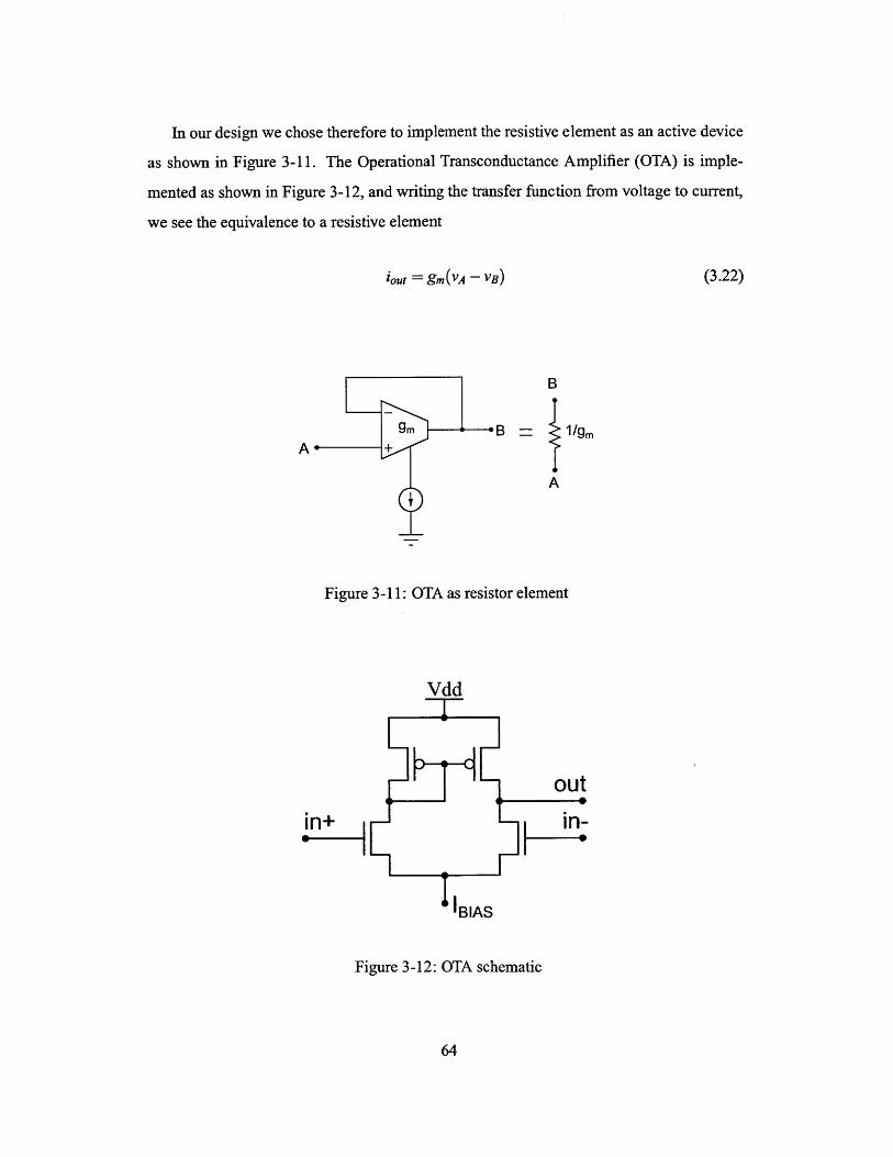
In our design we chose therefore to implement the resistive element as an active device
as shown in Figure 3-11. The Operational Transconductance Amplifier (OTA) is imple-
mented as shown in Figure 3-12, and writing the transfer function from voltage to current,
we see the equivalence to a resistive element
iout = gm(vA - VB) (3.22)
B
1/gm
A
A
Figure 3-11: OTA as resistor element
Vdd
in+out
-0
in-
IBIAS
Figure 3-12: OTA schematic
64

3.2.3.1 Constant gm Reference
To create the required current biasing for the OTA, as well as provide a simple method
for scaling the resistor value, we will use a constant gm current source [23] along with a
trimmable current mirror. The schematic of the current source reference is shown in Figure
3-13.
Vdd
VN
R
Figure 3-13: Current reference schematic
The current reference circuit also includes startup circuitry to ensure the fast settling
of the circuit nodes to their steady state values. The reference is Proportional to Absolute
Temperature (PTAT), and therefore provides a constant g, value for all devices referenced
to it. Assuming operation in the weak inversion regime of the transistors, we may write the
currents through the left and right NMOS devices
ileft = Ioe It
iright = MIoe t
(3.23)
(3.24)
65

Where -kT is the thermal voltage, kB is the Boltzmann constant, T absolute tempera-q
ture in Kelvin and q the electron unit charge. Io is the constant current at zero bias, VR is
the voltage across the resistor and K is the transistor's sub threshold slope factor in weak
inversion.
The PMOS current mirror ensures that ieft = iright, and therefore
VN N - VR+ M4t 4t
VR =- lnM (3.25)
We may now express the current reference as
ileft = iright = = InM (3.26)R icR
We may observe that the current reference is indeed proportional to absolute temperature,
but recalling the definition of the transistor transconductance gain
KJDSgm,= (3.27)
Ot
Thus this current reference will provide a constant transconductance to all devices con-
nected to it, independent of temperature change
gm = nInM = 1InM (3.28)Ot (-KR M)R
In our design we therefore set the constant resistor to a value of about 209i, and the
transistor ratio to 2. We implement a 6 bit current mirror, enabling us to scale the current
reference by up to a factor of 64 resulting in an effective resistance tuning range from
Rmin ~ 0.5 2 to Rmax ~ 30 92 as shown in Figure 3-14. This in turn enables us to compensate
for any variations in the capacitance LSB in order to ensure full coverage of an entire phase
quadrant.
66

520-
10-
5-
0'0 10 20 30 40 50 60
Trim Code
Figure 3-14: Theoretical effective resistance value
3.2.4 RC Polyphase Filter
In all of our derivations so far we have only considered the coverage of 900 of phase, in
a real system we require of course a full coverage of 360'. This requires us to enable the
creation of shifted versions of out input signal to cover all 4 quadrants. This is not a unique
requirement for our design, and also exists for other topologies, such as the current steering
DAC represented by the sine and cosine multipliers of the baseband current. This task is in
fact very commonplace in many systems which require the creation of orthogonal signals.
For our design we will address this issue by inserting an RC polyphase filter at the input
of the system before the amplifier, and selecting the appropriate quadrant with an additional
2 bits. Thus, we will phase shift the chosen quadrant by an additional 10 bit of precision
over the quadrant span resulting in an overall resolution of 12 bits.
A schematic showing the polyphase filter design is shown in Figure 3-15. The values
chosen for the resistors is Rp,0 y = 315 , and the value of the capacitors is Cp,,y = 210 fF.
The choice to use two stages of the polyphase filter as opposed to one was to reduce the
sensitivity to frequency variation at a cost of an additional amplitude loss of 3 dB at the
67

output [24]. This is shown in Figures 3-16 and 3-17.
lin+ Out1+ j out2+
Qout1+ Qout2+
lin- 3 ui out2-
OUti- Qout2-
Figure 3-15: RC polyphase filter schematic
In order to avoid asymmetrical loading of the polyphase filter by the common source
amplifier stage, a unity gain, source follower amplifier was implemented following a quadra-
ture select analog MUX. This allowed for the relevant output to be loaded by a small ca-
pacitance and thus not varying and affecting its output greatly.
3.3 Measurement Results
The PM was extensively tested in static scenarios as well as high data transfer rate to
demonstrate the extremely accurate and fast operation of the circuit and its fast settling
time. See Appendix A for a detailed explanation on the chip testing setup as well as the
data demodulation technique used to obtain the results below.
Due to extremely larger parasitic effects than were expected, the center frequency op-
eration of the circuit which enabled complete 360* coverage of phase had to be set to
approximately 420 MHz. This however does not affect any of the operating concepts of the
circuit and it still illustrates many of the conceptual ideas described above.
68

.100F -
2 100 10 10Normalized Frequency
Figure 3-16: One stage RC Polyphase filter response
102 10 100 10
F
In-phase- - - Quadrature
10 100Normalized Frequency
Figure 3-17: Two stage RC Polyphase filter response
69
1
0)_0
E
0
-50
U)C
X__
102
- In-phase- - - Quadrature
200u10 102
1
0.8
0.6
0.4
0.2
->
E
0r
-100
-200
10-2 10 1 102
-
- 41 1H
-150
10 2

3.3.1 Capacitor Trim
We start our measurements by adjusting the output bias voltage to be near half the supply
voltage (around 0.5 V) in order to obtain a 50% duty-cycle signal at the output. Choosing
the extreme and middle points of the varying capacitor bank, i.e. code words 0, 512 and
1023 should result in the extreme and middle phase points of a single quadrant. Comparing
the degree span of the top half to the bottom half gives us an indication about the tank's
frequency tuning. When the tank is tuned, the two halves should be equal, and their differ-
ence will be 0'. If the fixed capacitance is too low, the center frequency of the tank will be
higher than the actual carrier frequency and the result will be a quadrant sweep where the
bottom half covers a smaller degree span than the top half of the quadrant and alternately
if the fixed capacitance is too large.
Plotting the difference between the bottom half quadrant to the top half for each fixed
capacitance trim code results in the measurement plot shown in Figure 3-18. As can be
seen, for a trim code of C,im = 25 we observe an equilibrium and symmetry in the phase
sweep.
0.4
0.2-
0-
S -0.2 -
~0.caCO
-o -0.6-E
c -0.8-
-1.2- ,*
-1.4 --
-1.60 5 10 15 20 25 30
Fixed Capacitor Trim Code
Figure 3-18: Phase quadrant imbalance vs. fixed capacitor size trim
70

3.3.2 Resistor Trim
After calibrating the center frequency of the tank, we may now compensate for any vari-
ations in the resistor size or varying capacitor LSB size by modifying the active resistor's
current bias, thus changing the effective resistor value and the quality factor of the circuit.
Changing the resistor value will determine the phase coverage of a single quadrant, ideally
this should be 900, but we may choose a slightly larger coverage to ensure overlap between
quadrants and avoid missing codes. This is illustrated in Figure 3-19 showing the phase
coverage of one quadrant for several different resistor trim codes, and the expansions and
contraction of the phase coverage can be observed while maintaining the symmetry around
the code's center point, once again illustrating the concept of variable separation on the
system's behavior. Figure 3-20 shows the measurement results of the quadrant size, i.e. the
phase at the minimum capacitor code subtracted from the phase at the maximum capacitor
code, as a function of the resistor trim value which is inversely proportional to the resistor
size. We can see that for a code of about Rtrim = 5 we obtain roughly 90.9' quadrant phase
coverage.
50
40 -
30 -
20 -
0--Do 0CO
A-10-
-20- ..
-30 -_R =2
-40- R= 5..... Rtr = 9
-500 200 400 600 800 1000
Phase Code Word
Figure 3-19: Quadrant phase coverage for various resistor trim values
71
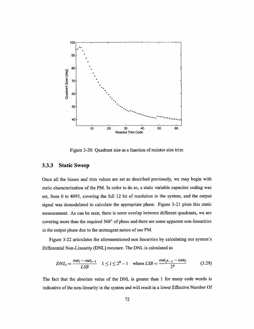
100
90-
80-0)
-0-
~0
50-
40 -
10 20 30 40 50 60Resistor Trim Code
Figure 3-20: Quadrant size as a function of resistor size trim
3.3.3 Static Sweep
Once all the biases and trim values are set as described previously, we may begin with
static characterization of the PM. In order to do so, a static variable capacitor coding was
set, from 0 to 4095, covering the full 12 bit of resolution in the system, and the output
signal was demodulated to calculate the appropriate phase. Figure 3-21 plots this static
measurement. As can be seen, there is some overlap between different quadrants, we are
covering more than the required 3600 of phase and there are some apparent non-linearities
in the output phase due to the arctangent nature of our PM.
Figure 3-22 articulates the aforementioned non linearities by calculating our system's
Differential Non-Linearity (DNL) measure. The DNL is calculated as
outi - outi-1I b Iout2b-1 -- outoDNL; = 1 <i<2 -1 where LSB= 2 b (3.29)
LSB---2
The fact that the absolute value of the DNL is greater than 1 for many code words is
indicative of the non-linearity in the system and will result in a lower Effective Number Of
72
- -

200-CU
150-
100-
50-
0'0 500 1000 1500 2000 2500 3000 3500 4000
Phase Code Word
Figure 3-21: Static phase sweep
Bits (ENOB).
All of these issues may be addressed by a simple digital pre-distortion look-up table. We
may match every code word to its actual phase value, and then when a requested phase is
given, the lookup table matches the closest appropriate code which will generate the desired
phase. Figure 3-23 illustrates this concept and shows the improved linearity achieved via
this simple technique.
Figure 3-24 illustrates that after pre-distortion we may find that in order to assure a DNL
value smaller than 1 for all code transitions, the effective number of bits of our system is
approximately 10.2 (disregarding one "rogue" value, if we wish to eliminate it as well our
ENOB drops to 9 bits).
73
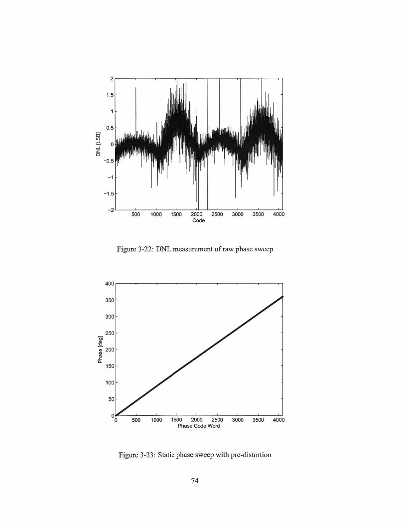
1.5
1
0.5
0-jz
-0.5
-1
-1.5 F
-2
400
a)
500 1000 1500 2000 2500 3000 3500 4000Code
Figure 3-22: DNL measurement of raw phase sweep
0 500 1000 1500 2000 2500 3000 3500 4000Phase Code Word
Figure 3-23: Static phase sweep with pre-distortion
74
lip 111,19~
Ir ' 1 1

1.
0.8-
0.6-
0.4 --
0.2
z 0
-0.2 -
-0.4 --
-0.6 --
-0.8 -
200 400 600 800 1000Code
Figure 3-24: DNL after pre-distortion and resolution reduction
3.3.4 Settling Time
To test the settling time performance of the circuit, a repetitive pattern was transmitted
causing a phase change of 900 in either direction, being the largest available step size
(recalling that greater phase changes swap between quadrants of the input signal rather than
change the tank capacitance). Figure 3-25(a) shows the demodulated signal step response
and 3-25(b) shows a zoomed-in view of the same response with the i1 limits marked
around the start and end phase in dashed lines.
It can be seen that our system indeed has a very fast settling time, which is in excellent
agreement with Eq. (3.13) at about 5 carrier cycles for settling to 1 of the final value. This
speed allows us, as mentioned earlier, to highly oversample the transmitted signal if desired
in order to improve the output spectrum.
75

90
80
70-
60-
50-
cow 40-
wc
30-
20-
10-
0-
0 50 100 150 200 250 300 350 400Carrier Cycles
(a)
90 - -
80-
70-
60-
D 50-
40--
30--
20-
10-
0
295 300 305Carrier Cycles
(b)
Figure 3-25: (a) Phase step settling time and (b) zoom-in
76
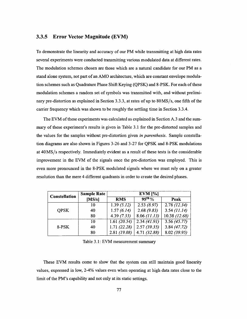
3.3.5 Error Vector Magnitude (EVM)
To demonstrate the linearity and accuracy of our PM while transmitting at high data rates
several experiments were conducted transmitting various modulated data at different rates.
The modulation schemes chosen are those which are a natural candidate for our PM as a
stand alone system, not part of an AMO architecture, which are constant envelope modula-
tion schemes such as Quadrature Phase Shift Keying (QPSK) and 8-PSK. For each of these
modulation schemes a random set of symbols was transmitted with, and without prelimi-
nary pre-distortion as explained in Section 3.3.3, at rates of up to 80MS/s, one fifth of the
carrier frequency which was shown to be roughly the settling time in Section 3.3.4.
The EVM of these experiments was calculated as explained in Section A.3 and the sum-
mary of these experiment's results is given in Table 3.1 for the pre-distorted samples and
the values for the samples without pre-distortion given in parenthesis. Sample constella-
tion diagrams are also shown in Figures 3-26 and 3-27 for QPSK and 8-PSK modulations
at 40 MS/s respectively. Immediately evident as a result of these tests is the considerable
improvement in the EVM of the signals once the pre-distortion was employed. This is
even more pronounced in the 8-PSK modulated signals where we must rely on a greater
resolution than the mere 4 different quadrants in order to create the desired phases.
Sample Rate EVM [%]Constellation [MS/s] RMS 9 5 th % Peak
10 1.39 (5.12) 2.53 (8.97) 2.78 (12.34)QPSK 40 1.57(6.14) 2.68(9.83) 3.54 (11.14)
80 4.39 (7.33) 8.06 (11.13) 10.38 (12.68)10 1.61 (20.54) 2.34 (41.91) 3.56 (45.77)
8-PSK 40 1.71 (22.28) 2.57 (39.35) 3.84 (47.72)80 2.81 (19.08) 4.71 (32.88) 8.02 (39.95)
Table 3.1: EVM measurement summary
These EVM results come to show that the system can still maintain good linearity
values, expressed in low, 2-4% values even when operating at high data rates close to the
limit of the PM's capability and not only at its static settings.
77

-0.5 0In-phase
0.5
N
Ia -C
-C
-C
(a) Without pre-distortion
0.8.
0.6-
0.4-
02
0 - - - -- - - . ..- .- . .. .-. .-- - - - - - - - .- -
.2
0.4
0.6.
-1 -0.5 0 5 1In-phase
(b) With pre-distortion
Figure 3-26: EVM measurements for QPSK modulation at 40 MS/s
-1 -0.5 0In-phase
0.5 1
a8
1
1
0.8
0.6
0.4
0.2
0
-0.2
-0.4
-0.6
-0.8
-1
(a) Without pre-distortion
-1 -0.5 0In-phase
Figure 3-27: EVM measurements for 8-PSK modulation at 40 MS/s
78
0.8-
0.6-
0.4-
* 0.2
0
0 -0.2
-0.4
-0.6.
-0.81
..
10.8
0.6
0.4
8 0.2
0 -0.2
-0.4
-0.6
-0.8
-1
0.5 1
(b) With pre-distortion
.. .... ... .. ...... .
------------- ---.. ...---------------- .----.

3.3.6 Power Spectrum
An important criteria of any transmitter is the Power Spectral Density (PSD) of its output.
Different communication protocols and regulatory bodies such as the Federal Communica-
tions Commission (FCC) and the European Telecommunications Standards Institute (ETSI)
define guidelines as to which levels of transmission power are allowed at various frequency
channels. The main purpose of these regulations is to ensure "peaceful coexistence" of
multiple transmitters in the same area, so as not to allow one to interfere too heavily with
its neighbor's transmission. These requirements are often described via masks which over-
lay the transmitters PSD output and require that the transmission power be below those
prescribed limits.
One such protocol is the Medical Implant Communication Services (MICS) [25], which
defines channels for transmissions by devices used in implanted medical devices [26]. This
protocol does not specify the modulation scheme, only that power levels out of the 6MHz
band of transmission be lower than 20dB compared to the carrier. To maximize the uti-
lization of the available bandwidth we will use a modulation scheme of 8-PSK allowing
us to encode 3 bits of information in every symbol transmitted. For simplicity we will not
preform any pulse shaping on the data transmitted and simply transmit random data and
look at the output spectrum.
The output PSD is calculated as described in Section A.4 and plotted alongside the
MICS spectral mask in Figure 3-28(a). We may observe that the side-lobes created by the
periodic sampling of the signal limited the maximum data rate we can use and still meet
the mask requirements to 1.25MS/s, which in turn translates to an effective data rate of
3.75 Mb/s. We have not however even come close to utilizing the full speed capability of
our PM. We may improve the output spectrum of our signal and eliminate some of these
low frequency repetition side-lobes by oversampling our signal prior to transmission and
increasing the sample rate. This allows us for example to obtain an Oversampling Ra-
tio (OSR) of 8, with a sample rate of 15 MSamples/s, a symbol rate of 1.875 MSymbols/s
and therefore an effective data rate of 5.625 Mb/s while still abiding by the spectral mask
requirements as shown in Figure 3-28(b). We have therefore improved our effective data
79

rate by 50% by simply utilizing oversampling enabled by the fast settling time of our sys-
tem.
0 00- - - -- -- --- - 0- - - -- - -- -- -
-5 -. 5
-10. -- 10
'2-15 - 15
~-20 - ------- C-20 -
-25 -25
-30 - -30
-40 -40-
-45 -45-
-50 -5W-6 -4 -2 0 2 4 6 -6 -4 -2 0 2 4 6
Offsetfmm Camer [MHz] Offset from Carer [MHz]
(a) No Oversampling, 3.75 Mb/s (b) x8 Oversampling, 5.625 Mb/s
Figure 3-28: 8-PSK modulation output PSD overlaid with MICS mask
Another widespread communication protocol is Global System for Mobile Communi-
cations (GSM) used in many cellular applications around the world. The power spectrum
requirements of GSM are very strict, calling, among other things, for 60 dB of attenuation
relative to the carrier at an offset of 400kHz [27]. In order to meet these requirements,
one of the methods used by the protocol is to modulate the transmitted data using Gaussian
Minimum Shift Keying (GMSK) modulation. GMSK is similar to Minimum Shift Key-
ing (MSK), which in turn is a form of Continuous Phase Modulation (CPM). In CPM the
phase of the signal is changed continuously, and not abruptly such as in QPSK or 8-PSK.
MSK has a constellation identical to that of QPSK, but allows transitions of only ±900 for
every symbol change, meaning that the signal will not have phase changes of 180'. This
allows considerable improvement of the output power spectrum since it eliminates high
frequency sharp edges and transitions in the signal. GMSK improves this yet further by
applying a Gaussian filter to the data before transmission [28], thus further shaping the
output spectrum.
Figure 3-29 shows the results of PSD measurement for data transmitted using GMSK
modulation and an OSR of 8. The spectrum does not fully comply with the mask, the
spectrum being higher from about 300kHz offset to around 1 MHz offset, with a maximum
80

deviation of 12.4 dB from the mask requirements. This is most likely due to the switching
nature of our system which introduces noise and raises the noise floor making it increas-
ingly difficult to meet the stringent requirements of the GSM protocol.
0-- 0-
10 - 1.5-0 O
Co -20-20
0-
0.30
sir 40-4
a. a.-50
-6060---
-1.5 -1 -0.5 0 0.5 1 1.5 -500 0 500Offset from Carrier [MHz] Offset from Carrier [ktz]
(a) (b)
Figure 3-29: (a) GMSK modulation output PSD overlaid with GSM mask and (b) zoom-in
3.4 Summary
An approach to achieve fast, high precision phase modulation for use in an outphasing
transmitter was presented and analyzed. The merits and design considerations of the pro-
posed approach were discussed. The switching of the capacitive load of a low-Q resonant
tank shows promise as being simple to implement and meeting the requirements for use in
such outphasing systems.
A proof-of-concept test chip implementing the proposed phase modulator was fabri-
cated in 65 nm CMOS and tested to verify performance and capabilities. It was shown to
be able to operate at speeds up to one fifth of the carrier cycle, with an accuracy of roughly
10.2 bits. The PM was tested as a stand-alone constant-envelope transmitter and shown
to maintain good linearity of less than 5% EVM while modulating data using QPSK and
8-PSK. The output power spectrum was analyzed and shown to comply with requirements
for broadcasting in the MICS bands and achieving very high data rates of up to 5.625 Mb/s
over a 6MHz band.
81

82

Appendix A
Data Demodulation
Following is a detailed explanation on how the data demodulation was done in order to ob-
tain the phase data from the output signals of the Low-Q Resonant Tank Phase Modulator
test chip. The method used here resembles the basic principles of general signal demodu-
lation in receivers [29], with a few nuances which help yield better numerical accuracy for
the results.
A.1 Test Setup
Figure A-i illustrates the testing setup used to capture the measurement results of the sys-
tem. The Low-Q Resonant Tank Phase Modulator test chip was flip-chip bonded to a
Printed Circuit Board (PCB) substrate to supply the various bias voltages as well as allow
communication with an FPGA unit. An RF source output was split, going to the real-time
oscilloscope as well as to the phase modulator. The output of the phase modulator was
also connected to the real-time scope as well as to a spectrum analyzer. An external clock
generator was used for the data baseband transfer.
83
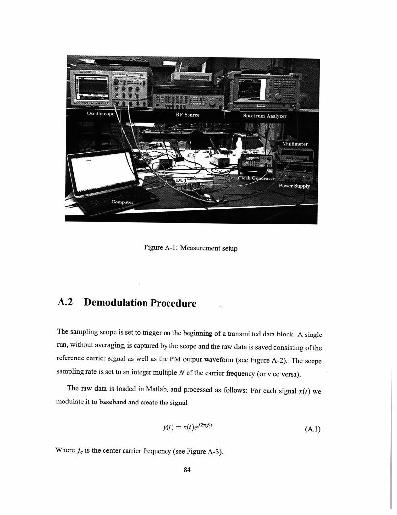
Figure A-1: Measurement setup
A.2 Demodulation Procedure
The sampling scope is set to trigger on the beginning of a transmitted data block. A single
run, without averaging, is captured by the scope and the raw data is saved consisting of the
reference carrier signal as well as the PM output waveform (see Figure A-2). The scope
sampling rate is set to an integer multiple N of the carrier frequency (or vice versa).
The raw data is loaded in Matlab, and processed as follows: For each signal x(t) we
modulate it to baseband and create the signal
y(t) = x(t)e u c' (A.1)
Where fe is the center carrier frequency (see Figure A-3).
84

-0.5
-1.5 POuPM Out jI- - - Reference '
-2385 390 395 400 405 410
Time [ns]
Figure A-2: Reference and PM output data from scope capture.carrier frequency 416.67 MHz, sampling rate 40GS/s
415
Data rate is 1OMS/s,
0.80
-50 100 150 200 250 300 350 400 450Time [ns]
Figure A-3: Modulated PM output (only real part displayed)
85

The signal is then filtered using a moving average filter, so
z(t) =y(t) *h(t) (A.2)
The filter consists of the number of points N which are the integer ratio between the sam-
pling frequency and the carrier frequency. Such a filter is simply a scaled window in the
time domain, or a sinc function in the frequency domain (see Figure A-4), whose zeros
occur at integer multiples of the carrier frequency. This allows to capture a very wide base-
band content of the signal and ensures the removal of artifacts caused by the carrier and its
harmonics as well as the sampling frequency (which in our case is also a harmonic of the
carrier and will be zeroed out). This wideband filter allows us to resolve very fast transi-
tions in the data and helps avoid masking of the fast phase transitions we wish to observe
by low-pass filtering them. The first N points of the filtered data are removed, since they
exhibit transient effects due to the finite length of the filter
1-
0.9-
0.8-
0.7-
0.6-
0.5 -
0.4-
0.3-
0.2-
0.1-
0-0.01
(D
E
0.1 1 10Frequency [fi
100
Figure A-4: Low-pass filter frequency response
86

The filtered data is now normalized to its average absolute value
z'(t) z(t) (A.3)(Iz(t)|)
Since we are dealing with phase modulated signals, the amplitude of these signals is
roughly constant, the normalization simply scales the signal's amplitude to 1.
Since we are mainly interested in the signal's phase in respect to the input carrier, we
now scale the PM output by the reference signal
zpm(t)Zfinal(t) = (A.4)
ref~t
This also eliminates any errors which occur due to drift or change in the reference's absolute
phase.
At this point, the signal zfinal(t) contains all the desired information. Its real and imag-
inary parts correspond to the In-phase and Quadrature components of the baseband signal
(see Figure A-5), and its phase is the sought after modulated phase value. To match this
value to the transmitted data, we need to sample the signal at the data rate, where the sample
offset may be set to the middle of the sample, and we may also apply a constant phase offset
in order to rotate the constellation to a desired starting point (see Figure A-6). Therefore
the sampled data may be represented by
d[n]= Z'inai(nT + ToSjset)Oe where T = (A.5)fbaseband
87
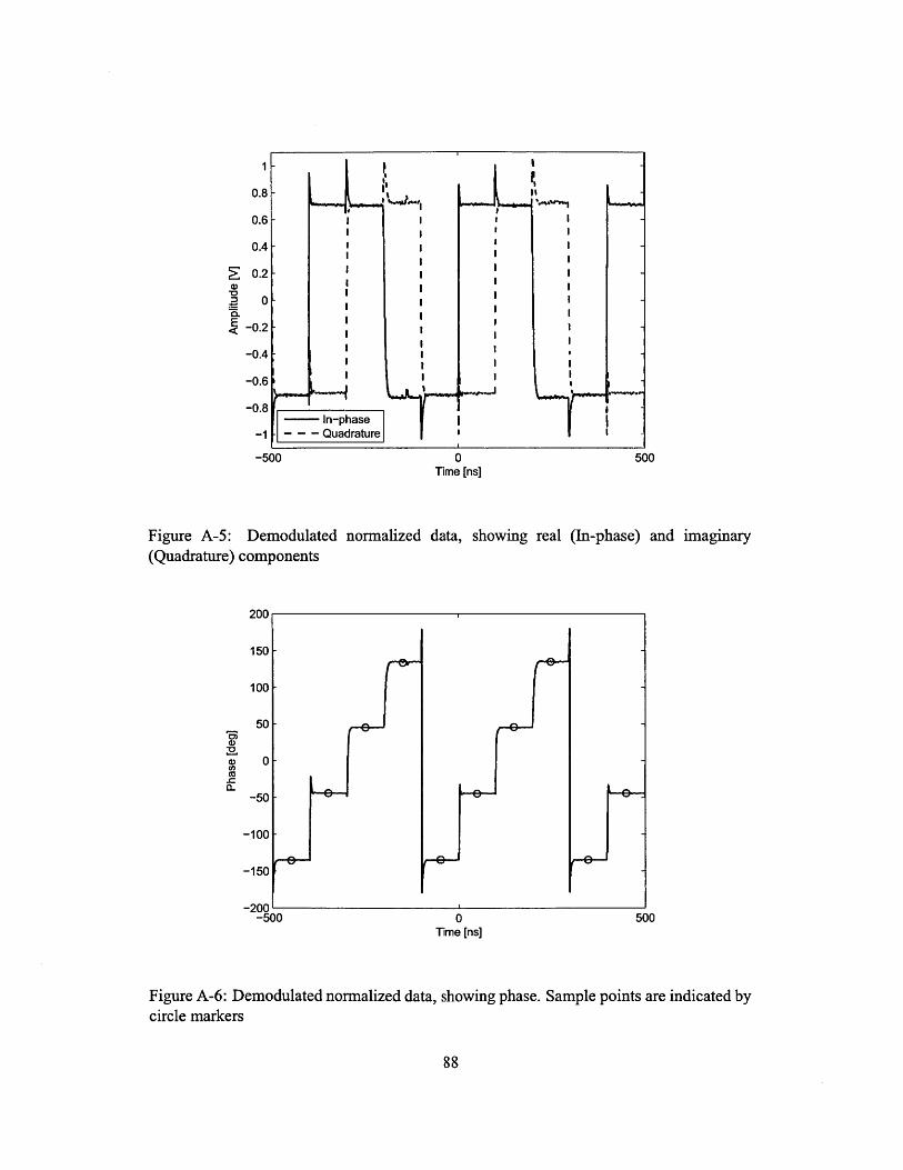
2:(D
E
-500 0Time [ns]
Figure A-5:(Quadrature)
,a;CD
CO-C
Demodulated normalized data, showing real (In-phase) and imaginarycomponents
200
150
100
50
0
-50
-100
-150
-200'-500 5000
Time [ns]
Figure A-6: Demodulated normalized data, showing phase. Sample points are indicated bycircle markers
88
500
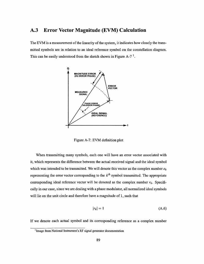
A.3 Error Vector Magnitude (EVM) Calculation
The EVM is a measurement of the linearity of the system, it indicates how closely the trans-
mitted symbols are in relation to an ideal reference symbol on the constellation diagram.
This can be easily understood from the sketch shown in Figure A-7 1.
Q
Figure A-7: EVM definition plot
When transmitting many symbols, each one will have an error vector associated with
it, which represents the difference between the actual received signal and the ideal symbol
which was intended to be transmitted. We will denote this vector as the complex number ek
representing the error vector corresponding to the kh symbol transmitted. The appropriate
corresponding ideal reference vector will be denoted as the complex number rk. Specifi-
cally in our case, since we are dealing with a phase modulator, all normalized ideal symbols
will lie on the unit circle and therefore have a magnitude of 1, such that
Irki = 1 (A.6)
If we denote each actual symbol and its corresponding reference as a complex number
I Image from National Instrument's RF signal generator documentation
89

related to their In-phase and Quadrature components
Sk = k+ jQk (A.7)
rk = Ik+ jk (A.8)
Then the error vector may be obtained by the subtraction of the ideal reference from the
actual signal
ek = sk - rk (A.9)
The magnitude of the error vector can now easily be calculated for each symbol as
Iekl = ISk - rk
= (Ik -Ik)+ j(Qk -Qk)I
= (Ik -) 2 + (Qk - k) 2 (A.10)
Now that we have defined the magnitude of the error vector for each transmitted symbol
we may define several statistical figures of merit which help characterize the linearity of
the system and how close it is to the desired ideal. Assuming a transmission of N symbols,
we may define the Root Mean Square (RMS) EVM as
N
ek12 NEVMRMS = N EI ek|2 (A.11)
rN |2 Nk=1NE Irkl
k=1
Where the last transition was possible in our case due to Eq. (A.6).
We may further define the peak EVM value as
EVMPeak = max IekI (A.12)k
Another useful definition is that of the 9 5 th percentile EVM. This value is obtained by
creating a histogram of the EVM values, and selecting the value which 95% of the samples
90

lie below it. From the above definitions we can conclude that the following relationship
always holds true
EVMRMS5 EVM95% 5 EVMPeak (A.13)
These definitions are illustrated below in Figure A-8. A population of 2000 symbols
were transmitted at 40 MS/s with 8-PSK modulation. The data was analyzed and sampled
as described in section A.2 and the EVM was divided into 50 histogram bins and plotted.
The dashed lines represent the various values corresponding to the RMS, 9 5'h percentile
and peak EVM values of this example.
1201RMS 1 95th Peak
Percentile
100- -
80 -
EMCO0 60-
z 40.
20-0 40
0 0.5 1 1.5 2 2.5 3 3.5 4EVM [%]
Figure A-8: EVM histogram example
91

A.4 Power Spectral Density (PSD) Calculation
The PSD of a signal was calculated using Welche's method for spectral estimation [30].
Basically taking the data signal, dividing it into several overlapping segments and window-
ing each one with a Hanning window [31]. We then calculate the absolute square of the
Fourier Transform of the windowed segments and average, effectively creating an averaged
modified periodogram.
The plots presented in this work are usually normalized to the peak output power, so
the units of the graphs are given in dBc/Hz, that is, power per unit frequency relative to
the carrier power. This enables simple comparison to standard communication protocol
spectral masks as presented in Section 3.3.6.
92

Bibliography
[1] T. H. Lee, The Design of CMOS Radio-Frequency Integrated Circuits, Second Edi-
tion. Cambridge University Press, 2 ed., Dec. 2003.
[2] L. Kahn, "Single-sideband transmission by envelope elimination and restoration,"Proceedings of the IRE, vol. 40, pp. 803 -806, July 1952.
[3] H. Chireix, "High power outphasing modulation," Proceedings of the Institute ofRa-dio Engineers, vol. 23, pp. 1370 - 1392, Nov. 1935.
[4] D. Cox, "Linear amplification with nonlinear components," Communications, IEEE
Transactions on, vol. 22, pp. 1942 - 1945, Dec. 1974.
[5] D. M. Pozar, Microwave Engineering. Wiley, 4 ed., Nov. 2011.
[6] Y.-C. Chen, K.-Y. Jheng, A.-Y Wu, H.-W. Tsao, and B. Tzeng, "Multilevel LINCsystem design for wireless transmitters," in VLSIDesign, Automation and Test, 2007.VLSI-DAT 2007. International Symposium on, pp. 1 -4, Apr. 2007.
[7] S. Chung, P. A. Godoy, T. W. Barton, E. W. Huang, D. J. Perreault, and J. L. Dawson,"Asymmetric multilevel outphasing architecture for multi-standard transmitters," inIEEE Radio Frequency Integrated Circuits Symposium, 2009. RFIC 2009, pp. 237-240, IEEE, June 2009.
[8] J. Hur, 0. Lee, K. Kim, K. Lim, and J. Laskar, "Highly efficient uneven multi-levelLINC transmitter," Electronics Letters, vol. 45, no. 16, pp. 837 -838, 2009.
[9] P. A. Godoy, S. W. Chung, T. W. Barton, D. J. Perreault, and J. L. Dawson, "A highlyefficient 1.95-GHz, 18-w asymmetric multilevel outphasing transmitter for widebandapplications," in Microwave Symposium Digest (MT), 2011 IEEE MTT-S Interna-
tional, p. 14, 2011.
[10] P. A. Godoy, S. W. Chung, T. W. Barton, D. J. Perreault, and J. L. Dawson, "A 2.5-GHz asymmetric multilevel outphasing power amplifier in 65-nm CMOS," in PowerAmplifiers for Wireless and Radio Applications (PAWR), 2011 IEEE Topical Confer-ence on, p. 5760, 2011.
[11] J. S. Walling, S. S. Taylor, and D. J. Allstot, "A class-G supply modulator and class-EPA in 130 nm CMOS," IEEE Journal ofSolid-State Circuits, vol. 44, pp. 2339-2347,Sept. 2009.
93
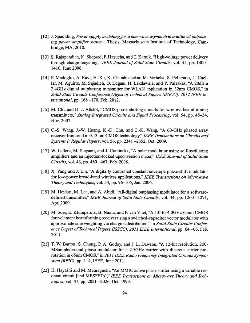
[12] J. Spaulding, Power supply switching for a mm-wave asymmetric multilevel outphas-ing power amplifier system. Thesis, Massachusetts Institute of Technology, Cam-
bridge, MA, 2010.
[13] S. Rajapandian, K. Shepard, P. Hazucha, and T. Karnik, "High-voltage power deliverythrough charge recycling," IEEE Journal of Solid-State Circuits, vol. 41, pp. 1400-1410, June 2006.
[14] P. Madoglio, A. Ravi, H. Xu, K. Chandrashekar, M. Verhelst, S. Pellerano, L. Cuel-lar, M. Aguirre, M. Sajadieh, 0. Degani, H. Lakdawala, and Y. Palaskas, "A 20dBm2.4GHz digital outphasing transmitter for WLAN application in 32nm CMOS," inSolid-State Circuits Conference Digest of Technical Papers (ISSCC), 2012 IEEE In-ternational, pp. 168 -170, Feb. 2012.
[15] M. Chu and D. J. Allstot, "CMOS phase-shifting circuits for wireless beamformingtransmitters," Analog Integrated Circuits and Signal Processing, vol. 54, pp. 45-54,Nov. 2007.
[16] C.-S. Wang, J.-W. Huang, K.-D. Chu, and C.-K. Wang, "A 60-GHz phased arrayreceiver front-end in 0.13 um CMOS technology," IEEE Transactions on Circuits andSystems I: Regular Papers, vol. 56, pp. 2341 -2352, Oct. 2009.
[17] W. Laflere, M. Steyaert, and J. Craninckx, "A polar modulator using self-oscillatingamplifiers and an injection-locked upconversion mixer," IEEE Journal of Solid-StateCircuits, vol. 43, pp. 460 -467, Feb. 2008.
[18] X. Yang and J. Lin, "A digitally controlled constant envelope phase-shift modulatorfor low-power broad-band wireless applications," IEEE Transactions on MicrowaveTheory and Techniques, vol. 54, pp. 96-105, Jan. 2006.
[19] M. Heidari, M. Lee, and A. Abidi, "All-digital outphasing modulator for a software-defined transmitter," IEEE Journal of Solid-State Circuits, vol. 44, pp. 1260 -1271,Apr. 2009.
[20] M. Soer, E. Klumperink, B. Nauta, and F. van Vliet, "A 1.0-to-4.OGHz 65nm CMOSfour-element beamforming receiver using a switched-capacitor vector modulator withapproximate sine weighting via charge redistribution," in Solid-State Circuits Confer-ence Digest of Technical Papers (ISSCC), 2011 IEEE International, pp. 64 -66, Feb.2011.
[21] T. W. Barton, S. Chung, P. A. Godoy, and J. L. Dawson, "A 12-bit resolution, 200-MSample/second phase modulator for a 2.5GHz carrier with discrete carrier pre-rotation in 65nm CMOS," in 2011 IEEE Radio Frequency Integrated Circuits Sympo-sium (RFIC), pp. 1-4, IEEE, June 2011.
[22] H. Hayashi and M. Mauraguchi, "An MMIC active phase shifter using a variable res-onant circuit [and MESFETs]," IEEE Transactions on Microwave Theory and Tech-niques, vol. 47, pp. 2021 -2026, Oct. 1999.
94

[23] S. Mandal, S. Arfin, and R. Sarpeshkar, "Fast startup CMOS current references,"in Circuits and Systems, 2006. ISCAS 2006. Proceedings. 2006 IEEE InternationalSymposium on, p. 4pp, 2006.
[24] J. Xie, A. Do, K. Yeo, and C. Boon, "Analysis and design of RC polyphase networkfor quadrature signal generation in the 2.45 GHz ISM band," in Integrated Circuits,2007. ISIC'07. International Symposium on, p. 430433, 2007.
[25] FCC, "e-CFR: title 47: Telecommunication," Jan. 2012.
[26] J. Bohorquez, A. Chandrakasan, and J. Dawson, "A 350 uW CMOS MSK transmitterand 400 uW OOK super-regenerative receiver for medical implant communications,"IEEE Journal ofSolid-State Circuits, vol. 44, pp. 1248 -1259, Apr. 2009.
[27] ETSI, "Digital cellular telecommunications system (Phase 2+): Radio transmissionand reception," Synchronization in UTRAN, Stage, vol. 2, 1999.
[28] ETSI, "Digital cellular telecommunications system (Phase 2+); universal mobiletelecommunications system (UMTS); LTE; anonymous communication rejection(ACR) and communication," 2009.
[29] A. F. Molisch, Wireless Communications. Wiley, 2 ed., Dec. 2010.
[30] P. Welch, "The use of fast fourier transform for the estimation of power spectra: Amethod based on time averaging over short, modified periodograms," IEEE Transac-tions on Audio and Electroacoustics, vol. 15, pp. 70 - 73, June 1967.
[31] A. V. Oppenheim and R. W. Schafer, Discrete-Time Signal Processing (3rd Edition).Prentice Hall, 3 ed., Aug. 2009.
95
![ANALOG & DIGITAL MODULATION TECHNIQUES: AN OVERVIEW · the demodulation and decoding techniques [1, 2]. ... Frequency Modulation proves to be better in comparison to amplitude modulation](https://img.pdfslide.net/doc/110x75/60261ff7e0783b6fc7233922/analog-digital-modulation-techniques-an-overview-the-demodulation-and-decoding.jpg)