Embed Size (px)
Citation preview

Altera Corporation 1AN-311-1.0 Preliminary
Application Note 311
ASIC to FPGA DesignMethodology & Guidelines
Introduction The cost of designing ASICs is increasing every year. In addition to the non-recurring engineering (NRE) and mask costs, development costs are increasing due to ASIC design complexity. Issues such as power, signal integrity, clock tree synthesis, and manufacturing defects can add significant risk and time-to-market delays. To overcome the risk of re-spins, high NRE costs, and to reduce time-to-market delays, FPGAs offer a viable and competitive option to ASIC development.
Programmable logic has progressed from being used as glue logic to today’s FPGAs, where complete system designs can be implemented on a single device. The number of gates and features has increased dramatically to compete with capabilities that have traditionally only been offered through ASIC devices. Figure 1 illustrates the evolution of FPGA applications that has led to higher density devices, intellectual property (IP) integration, and high-speed I/O interconnects technology. All of these elements have allowed FPGAs to play a central role in digital systems implementations. With the availability of multimillion-gate FPGA architectures, and support for various third-party EDA tools, designers can use a design flow similar to that used for ASIC devices to create system-on-a-programmable-chip (SOPC) designs in FPGAs.
This document addresses the FPGA design guidelines and methodologies that can be applied for better FPGA device performance and area utilization. Additionally, this document explains new features, such as SOPC Builder and the MegaWizard® Plug-In Manager, both available in the Altera® Quartus® II software tools, that are used to facilitate and simplify a true system on a programmable chip solution. And finally, this document draws analogies, pro and con, between typical FPGA and ASIC design processes.
July 2003, ver. 1.0

2 Altera CorporationPreliminary
ASIC to FPGA Design Methodology & Guidelines ASIC & FPGA Design Flows
Figure 1. Application of FPGA Devices from 1985 to the Present
ASIC & FPGA Design Flows
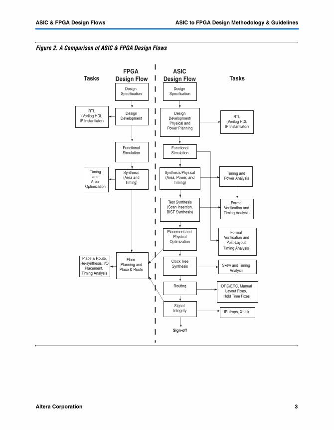
Typical ASIC and FPGA design flows are shown in Figure 2. The back-end design of an ASIC device involves a wide variety of complex tasks, including placement and physical optimization, clock tree synthesis, signal integrity, and routing using different EDA software tools. When compared to ASIC devices, the physical, or back-end, design of FPGA devices is very simple and is accomplished with a single software tool, the Quartus II software. This not only reduces the complexity of the design process, but also significantly reduces cost. This document discusses and compares each of the tasks involved in the design flows, for both FPGA and ASIC devices.
Glue Logic
Complex Control
SOPC Design
Equations Schematics
Control Logic
Synthesis Macrofunctions
Second-generation Synthesis IP Megafunctions
Block-based Design
Increasing PLD
Complexity
1985 1990 20031995
Altera Corporation 3Preliminary
ASIC & FPGA Design Flows ASIC to FPGA Design Methodology & Guidelines
Figure 2. A Comparison of ASIC & FPGA Design Flows
Design Specification
Design Development/ Physical and
Power Planning
Functional Simulation
Synthesis/Physical (Area, Power, and
Timing)
Test Synthesis (Scan Insertion, BIST Synthesis)
Placement and Physical
Optimization
Clock Tree Synthesis
Routing
Signal Integrity
Sign-off
Timing and Power Analysis
Formal Verification and Timing Analysis
Formal Verification and
Post-Layout Timing Analysis
Skew and Timing Analysis
DRC/ERC, Manual Layout Fixes,
Hold Time Fixes
IR drops, X-talk
Design Specification
Design Development
Functional Simulation
Synthesis (Area and Timing)
Floor Planning and Place & Route
ASIC Design Flow
FPGA Design Flow
RTL (Verilog HDL
IP Instantiator)
Timing and
Area Optimization
Place & Route, Re-synthesis, I/O
Placement, Timing Analysis
TasksTasks
RTL (Verilog HDL
IP Instantiator)

4 Altera CorporationPreliminary
ASIC to FPGA Design Methodology & Guidelines Design Specification
Design Specification
Design specification consists of defining specifications, including the following:
■ I/O standards, the number of I/O pins, and the location of the I/O pins for various standards
■ Global clocks and their frequency requirement■ Memory requirements■ Test methodology■ Selection of the FPGA family and device, including the speed grade
You must define each of the above specifications, because every FPGA family supports different I/O standards, and the devices within a family have different numbers of I/O pins.
I/O Specification
Selection of an FPGA device depends on considerations such as speed grade, signaling technology, termination technology, available logic elements (LEs), external reset, the number of global clock networks, and most importantly, the number of I/O pins available and the supported I/O standards. I/O resources vary depending upon the device and family. To meet today’s challenges of design complexity, and also to support complex I/O standards, Altera devices support a wide variety of I/O standards.
The ASIC design methodology consists of instantiating I/O pads for a design by specifying the technology I/O buffers in a Verilog HDL or VHDL file to perform simulation and synthesis. The I/O file will be a top-level file, and it instantiates the top-level design, as shown in Figure 3.

Altera Corporation 5Preliminary
Design Specification ASIC to FPGA Design Methodology & Guidelines
Figure 3. I/O Specification, with the Top-Level Design
After the design is handed over to the foundry, the io.v and io.vhd files are taken out and replaced with the technology I/O pads.
In FPGA design flow, third-party synthesis tools provide the option of synthesizing the design with or without I/O pads. Synthesizing with I/O pads provides a good estimate of the delay through the I/O buffers. Actual I/O assignment is done within the Quartus II software, using the Assignment Editor (Assignments menu), as shown in Figure 4. The designer is given the option for the synthesized design, including I/O pads, to be replaced by a specific I/O standard within the Quartus II software, or a specific I/O standard can be added to the top level design. These choices are both presented before place-and-route.
f For additional information, see the Using the Assignment Editor in the Quartus II Software white paper.
io.v/vhd
oe oe
oe
oeoe
oe
oe
top.v/vhd
Module A Module B
Module DModule C

6 Altera CorporationPreliminary
ASIC to FPGA Design Methodology & Guidelines Design Specification
Figure 4. Quartus II I/O Assignment Editor
f Altera FPGA devices support a wide variety of I/O standards. For information on the supported I/O standards in a specific Altera device, see the device-specific Altera data sheet.
Number of I/O Pins
You must determine the exact number of I/O pins used in the design. This number will ultimately be used to decide the type of package and the total number of pins required out of the package.
Location of I/O Pins
To minimize potential problems pertaining to board layout, I/O pin location must be given careful consideration. Incorporating high-speed signals in a board design requires minimizing via interconnects and cross-over signals to simplify the routing process. In an FPGA flow, because I/O banks support specific I/O standards, a designer must know the different I/O standards that the device can support so that modules in the design that require a certain I/O standard can be physically placed near the corresponding I/O bank.

Altera Corporation 7Preliminary
Design Specification ASIC to FPGA Design Methodology & Guidelines
f To learn more about the location of I/O banks and supported standards within an I/O bank, see the device-specific Altera data sheets.
I/O Timing
I/O timing is affected by the I/O standard and the drive strength. To meet I/O requirements, Altera FPGAs have I/O pins with registers. The device uses these registers depending on the clock setup time (tSU) and clock-to-output delay (tCO) requirements. These registers are enabled by setting constraints within the Quartus II software at the top level of the design hierarchy, such as the Fast Input Register and Fast Output Register, to determine register placement for I/O timing.
Number of Global Clocks
It is necessary to identify the number of clocks needed in a design in order to determine what type of FPGA can be used. There is usually an upper limit to the number of different clocks that can exist in a design. Clock tree insertion is a manual process in an ASIC flow, whereas in an FPGA flow it is an automatic process.
f For more information on clock tree synthesis and clock requirements, refer to “Clock Tree Synthesis” on page 42.
Memory Requirements
Identifying embedded dynamic random access memory (DRAM) and SRAM capacity and speed requirements is an integral part in the technology selection process and needs to be accomplished early in the process. Stratix devices have up to 4 Mbits of embedded memory within various sizes of memory blocks that can be used in different kinds of applications. Memory capacity is higher in ASIC technology, but integrating and testing this memory in an ASIC device requires significantly more work. In an FPGA flow, Quartus II software tools allow users to automatically arrange memory blocks to meet the system requirement, and no user instantiation is necessary. In an ASIC flow, integrating and testing embedded memory usually involves instantiating a special module in the register transfer level (RTL) design, as well as creating custom circuitry around the RAM blocks for testing.
f For more information on memory requirements and available configurations in an FPGA, refer to “Specification of External & Internal Memory” on page 26.

8 Altera CorporationPreliminary
ASIC to FPGA Design Methodology & Guidelines Design Specification
Phase-Locked Loop (PLL) Requirements
Identifying the number of PLLs needed in the design impacts the type and family of devices that can be selected in FPGA design flows. Inserting PLL circuitry in an ASIC device is typically a manual process accomplished by instantiating special PLL blocks in the design. PLLs are instantiated in the FPGA design after creating a configurable PLL with the MegaWizard Plug-In Manager tool available within the Quartus II software. This process is usually automatic in the Quartus II software. The number of PLLs available in FPGA technology is usually limited, whereas PLL quantities are virtually unlimited in ASIC technology. Stratix devices support up to 12 PLLs.
f For more information on the number and type of PLLs supported in a design, refer to the device-specific Altera data sheets.
Test Methodology
ASIC testing and fault coverage is an important aspect of the ASIC development process. Scan insertion, built-in self-test (BIST), signature analysis, IDDQ, and automatic test pattern generation (ATPG) all have to be considered and analyzed within an ASIC design flow. ASIC testing typically involves test vector generation, using ATPG tools to test the device for manufacturing defects under the “single stuck-at” model. ATPG is usually performed after completion of scan insertion. Scan insertion is performed to improve the obtained fault coverage by reducing the sequential testing problem to a combinatorial testing problem. Using FPGA technology, you do not need to worry about any device testing, because FPGA devices are pre-verified at the factory. In these devices, most logic functions are exhaustively tested by downloading different images into the device. Therefore, compared to ASIC devices, FPGA devices are much more likely to be defect-free after customer delivery.
Unlike FPGAs, where the top-level I/O pads can be synthesized by the synthesis tools, and boundary scan is already incorporated for test purposes, ASIC design flow generally requires extensive manual effort to insert and simulate boundary scan on top of the device logic, often using third-party EDA tools. Also, unlike FPGAs, ASIC test methodology requires sequential propagation of test vectors through all flip-flops of a design to identify single stuck-at-faults after device manufacturing. Due to a large number of flip-flops, the scan chain is broken down into many manageable chains, such that several chains can be tested in parallel on a tester. Due to a high number of scan chains and the limited number of I/O pins available on a package, an ASIC’s I/O pins are manually multiplexed with scan chain outputs so that the same pins can be used as functional pins in regular operation mode, and scan chain output pins in test mode.
Altera Corporation 9Preliminary
Design Development ASIC to FPGA Design Methodology & Guidelines
Clock Frequencies
The circuit’s speed will be another deciding factor in choosing the appropriate Altera FPGA for your design.
Number of Simultaneously Switching Outputs (SSOs)
The number and the placement of SSOs has a direct impact on the number of power and ground pins that an ASIC requires. This is usually not an issue with an FPGA, because the placement and number of power and ground pins is fixed and assigned through the Quartus II software.
FPGA Device Sizing
You must estimate the potential size of the logic required so that power and heat dissipation requirements can be estimated. After the size of the logic is estimated and operating frequencies are recognized, the approximate size and speed grade of the device can be selected.
Altera FPGAs also support vertical migration within the same package. In this context, you can migrate between devices whose dedicated pins, configuration pins, and power pins are the same for a given package across device densities. For example, you can migrate a design from an EP1S10B672C6 device to an EP1S20B672C6 device in the 672-pin package.
Power Requirement
Perform preliminary power analysis, based on the estimated logic size and speed, to determine the device power requirement. This usually leads to defining the device’s cooling and package requirements.
Design Development
Design development is comprised of the following processes for both FPGAs and ASICs.
■ Specification of the methodology (top-down or bottom-up)■ RTL coding guidelines for better performance■ Hierarchical design partitioning■ Specification of the external and internal memory■ IP availability and flow
10 Altera CorporationPreliminary
ASIC to FPGA Design Methodology & Guidelines Design Development
Specification of the Methodology
FPGA design methodology supports both top-down and bottom-up design methodology. FPGA design flows support modular design approaches for bottom-up methodology, and hierarchical design partitioning for top-down design methodology, similar to the process used for ASIC devices.
f For more information on design planning and different design approaches, see the following documents.
■ AN 226: Synplify & Quartus II Design Methodology■ AN161: Using the LogicLock Methodology in the Quartus II Design
Software■ AN 165: Synplify & Quartus II LogicLock Design Flow
RTL Coding Guidelines
Following simple design guidelines can improve device performance and design debugging capabilities. This section explains the following common design guidelines, which improve device performance by taking advantage of the FPGA architecture.
■ Synchronous versus asynchronous designs■ Synchronous versus asynchronous resets■ Gated clocks versus clock enables■ Using clock dividers■ Efficient use of clock-enables■ Using Altera PLLs to reduce clock skew■ Using data pipelining■ Using encoding schemes■ Using look-ahead techniques■ Using logic duplication■ Using internal buses
Synchronous vs. Asynchronous Designs
The two RTL code examples in this section show the differences between synchronous and asynchronous counters.
Synchronous DesignIn synchronous designs, all registers are clocked by one global clock, a primary input to the design. Synchronous designs are free from combinatorial feedback loops and delay lines. The following RTL code is an example of a synchronous counter.
Altera Corporation 11Preliminary
Design Development ASIC to FPGA Design Methodology & Guidelines
module sync_counter (clk,count_en,reset,count_out);
input clk,count_en,reset;output [3:0] count_out;reg [3:0] count_out;
always @(posedge clk) beginif (~reset)
count_out = 4’b0000;else if (count_en == 1’b1) begin
if (count_out == 4’b1111) count_out = 4’b0000;
else count_out = count_out + 1’b1;end
end
endmodule
Asynchronous DesignAsynchronous behavior occurs when a signal passes between two different clock domains due to different clock frequencies, gated clocks, or a modular place-and-route approach where large blocks of logic belonging to the same clock domain are not synchronized. The worst problem caused by an asynchronous signal is potential meta-stability in the destination register, because the signal state can be changing at the same time as the active clock edge of the destination register. You can avoid this meta-stability hazard by putting two extra stages of flip-flops before the destination register. If the signal does cause meta-stability, stabilize it by passing it through the two extra flip-flops before it reaches its intended register. The other problem caused by asynchronous signals is that the sampling clock at the receiving end may be too slow compared to the initiating clock, which causes the signal to be completely missed. In this scenario, a good handshake protocol must be implemented between asynchronous blocks of a device to ensure proper device operation. Figure 5 shows an example of an asynchronous design with multiple clocks asynchronous to each other, and the signal passing from one clock domain to another.

12 Altera CorporationPreliminary
ASIC to FPGA Design Methodology & Guidelines Design Development
Figure 5. An Asynchronous Design with Two Clocks Note (1)
Note to Figure 5:(1) Clk1 and Clk2 have different clock sources.
Typical design styles that contribute to asynchronous circuits include the following:
■ Gated clocks■ Latch inferences■ Multiple clocks■ Derived clocks
One of the disadvantages of asynchronous logic is that the existence of race conditions is an inherent problem with this type of logic. An example of an asynchronous counter is shown in the RTL code below.
module async_counter(clk,count_en,reset,count_out);
input clk,count_en,reset;output [3:0] count_out;reg [3:0] count_out;wire gated_clk = clk & count_en;
always @(posedge gated_clk or negedge reset) begin
if (~reset) count_out <= 4’b0000;
else beginif (count_out == 4’b1111) count_out <= 4’b0000;
else count_out <= count_out + 1’b1;
endendendmodule
CLKCLK
D Q D Q
clk 1 clk 2

Altera Corporation 13Preliminary
Design Development ASIC to FPGA Design Methodology & Guidelines
Synchronous vs. Asynchronous Resets
An asynchronous reset is defined as a way of clearing the contents of a register, independent of the associated clock. ASIC libraries consist of registers with and without a built-in reset/clear pin. A register with a built-in reset/clear pin is bigger than a register without one.
ASIC designers like to use registers with no built-in reset pins to obtain extra speed and area in a design by using an external gate on the data path of the register for a reset. When the reset is routed through the data pin, the clock must be running when the reset is asserted. Conversely, a synchronous reset signal is treated as any other data signal, so that no extra care is needed during the routing and timing optimization phase.
In ASIC designs, internally generated asynchronous resets from a state machine can cause problems in scan testing. A typical problem results from the shifting of test vectors through the flops of the state machine, which triggers unintended resets. This is not an issue for FPGAs, which are not scan tested.
Instead of gating the reset signal, if ASIC designers use registers with a built-in reset/clear pin, then asynchronous reset is controlled by a device’s primary input and buffered like a clock tree to reach all of the asynchronous reset pins of all of the device registers. In ASICs, a reset tree must be generated just like a clock tree. Use timing analysis or an independent start signal to prevent different state machines from getting out-of-sync immediately after the reset release.
In FPGAs, a reset tree is already in place. All registers have a built-in asynchronous reset, so no area savings are attained by not utilizing this reset capability. Safe design practice must be followed to ensure everything is in synch immediately after the reset signal is released.
Gated Clocks vs. Clock Enables
Clock gating is used in ASIC designs for power optimization. For example, if data has to be written to memory only when the write enable signal is high, then the clock can be gated with the write enable so that switching of the register takes place only when write enable is high. Gated clocks can introduce glitches and clock incorrect data due to the delay associated along the combinatorial path. The following RTL code is an example of clock gating, and the corresponding schematic is shown in Figure 6.

14 Altera CorporationPreliminary
ASIC to FPGA Design Methodology & Guidelines Design Development
module gated_clk(in,out,en,clk);input in,clk,en;output out;reg out;wire gate_clk;assign gate_clk = clk & en;always @(posedge gate_clk) begin
out <= in;end
endmodule
Figure 6. Clock Gating
The timing diagram shown in Figure 7 shows the glitch associated with clock gating.
Figure 7. Issues Associated with Clock Gating
D Q
Clk
Clk
En
gate_clock
Clk
En
Clk_en
Output

Altera Corporation 15Preliminary
Design Development ASIC to FPGA Design Methodology & Guidelines
FPGAs have a clock enable pin that can be used to avoid the gate clocking. Using the clock enable pin to disable the clocking of the flip-flop does not mean that the flip-flop is not getting clocked. It merely means that the current state of the flip-flop is clocked continuously. An example of this implementation of the flip-flop is shown in Figure 8.
Figure 8. A Clock Enable Pin Disabling Clocking of a Flip Flop
The following RTL code illustrates the modifications to the Figure 8 example, using the clock enable pin.
module clock_en(in,out,clk,data_en);input in,clk,data_en;output out;reg out;
always @(posedge clk) beginif (data_en)
out <= in;else
out <= out;endendmodule
Figure 9 shows the schematic for this clock enable code.
Figure 9. FPGA Devices’ Built-in Clock Enable Resource
clk
Din Q
DFF Cell
Q
CE
clk
D
D Q
CE
CLK
in out
data_en
clk

16 Altera CorporationPreliminary
ASIC to FPGA Design Methodology & Guidelines Design Development
Using Clock Dividers
Feeding the Q bar output to the data input is a widely used concept of clock division, known as ripple clock division. The following RTL code is an example of this type of divider.
module ripple_clk_divider(clk,data_in,data_out);input clk,data_in;output data_out;reg data_out;reg temp_clk;
always @(posedge clk)temp_clk <= ~temp_clk;
always @(posedge temp_clk)data_out <= data_in;
endmodule
Figure 10 shows the schematic for this code example.
Figure 10. Ripple Clock Division
The clock enable resource is used to divide a clock to reduce the ripple effect by synchronous clock division, as shown in the following RTL code example.
D Q
CE
CLK Q
data_in
temp_clk
D Q
CLK Q
clk

Altera Corporation 17Preliminary
Design Development ASIC to FPGA Design Methodology & Guidelines
module clock_divider_ce(clk,data_in,data_out);input clk,data_in;output data_out;reg data_out;reg temp_clk;
always @(posedge clk)temp_clk <= ~temp_clk;
always @(posedge clk) beginif (temp_clk)
data_out <= data_in;end
endmodule
Figure 11 shows the schematic for this code.
Figure 11. Synchronous Clock Division
Efficient Use of Clock Enables
There are situations in which the combinatorial logic that drives a register’s clock enable pin might be in the critical path. Clock enables are not accessible via the look-up table (LUT) in the same LE. Thus, if a logic function drives the clock enable of a flip-flop, then the clock enable is implemented in an external LUT with an associated logic and routing delay. To decrease the number of layers of logic, it is sometimes possible to implement the same clock enable in the data path with a multiplexer.
The following example shows RTL code that will reduce the number of logic levels.
D Q
CE
CLK Q
data_in
temp_clk
D Q
CLK Qclk

18 Altera CorporationPreliminary
ASIC to FPGA Design Methodology & Guidelines Design Development
module inefficient_ce(clk,datain,rwn,csn,asn,dataout);input clk,datain,rwn,csn,asn;output dataout;reg dataout;
always @(posedge clk)begin
if ((rwn == 1’b0) && (csn == 1’b0) && (asn == 1’b0))
dataout <= datain;end
endmodule
Figure 12 shows the schematic for the above code.
Figure 12. RTL Modification to Reduce the Number of Logic Levels
Using the following RTL code, the number of logic levels that drive the register’s clock enable can be reduced from one to zero LUTs.
in
in
datain
clk
rwn
csn
asn
S
R
D Q
CE
dataout
GND
out
outin(0)
in(1)out
outin(0)
in(1)in out

Altera Corporation 19Preliminary
Design Development ASIC to FPGA Design Methodology & Guidelines
module efficient_ce(clk,datain,rwn,csn,asn,dataout);
inputclk,datain,rwn,csn,asn;outputdataout;reg dataout;
always @(posedge clk)begin
if (csn == 1’b0) dataout <= (datain && (rwn == 1’b0) && (asn
== 1’b0))|| (dataout && rwn == 1’b1)|| (dataout && asn == 1’b1);
end
endmodule
Figure 13 shows the schematic for this RTL code.
Figure 13. Reduction of Logic Levels from One to Zero LUTs
1 Unless gate clocking is the only alternative, implement the design taking advantage of the clock enable resource.
in
datain
clk
rwn
csn
asn
out
out
in(0)
in(1)
out
S
R
D Q
CE
dataout
GND
in
out
in(0)
in(1)
in(1)
in(0)out
out
in(1)
in(0)
in(0)
in(1)
out
in out
in(0)
in(1)

20 Altera CorporationPreliminary
ASIC to FPGA Design Methodology & Guidelines Design Development
Using PLLs to Reduce Clock Skew
Altera PLLs can provide multiple clock sources to be used off-chip with the minimum possible skew. The RTL implementation shown below, and the schematic representation shown in Figure 14, describes how to drive eight pins that are three times the input clock. The PLL is used to multiply the input clock frequency by six, and a toggle flip-flop is used to obtain three times the input frequency. The Quartus II software MegaWizard Plug-in Manager generates the instantiated module pllx2, shown in Figure 14.
module off_chip(clk100in,clk300out);
inputclk100in;wireclk600;
output[7:0]clk300out;reg [7:0]clk300out;
reg clk300int /* synthesis syn_preserve = 1 */;
pllx2 U1(.inclock(clk100in),.clock1(clk600));
always @(posedge clk600)begin
clk300int <= ~clk300int;end
always @(posedge clk600)begin
clk300out[0]<=~clk300int;clk300out[1]<=~clk300int;clk300out[2]<=~clk300int;clk300out[3]<=~clk300int;clk300out[4]<=~clk300int;clk300out[5]<=~clk300int;clk300out[6]<=~clk300int;clk300out[7]<=~clk300int;
end
endmodule

Altera Corporation 21Preliminary
Design Development ASIC to FPGA Design Methodology & Guidelines
Figure 14. Altera PLL as a Source to Multiple Clocks
1 Unless gate clocking is the only alternative, implement the design taking advantage of the clock-enable resource.
Using Data Pipelining
FPGAs have many registers because there is a flip-flop available in each logic element, and these registers can be used to improve the device performance without incurring any area penalty. Data pipelining is an important concept that can be used to increase device performance by inserting registers to break a long combinatorial path. Figure 15 shows the concept of pipelining.
Figure 15. Illustration of Data Pipelining
1 Even though data pipelining increases design performance, be sure to equalize data and control path latency, and modify the test benches to accommodate signal capture from the introduced registers.
S
R
D Q
inclock clock1
pllx2
clk100in
External ClockSource
Altera FPGATo ExternalDevice
clk300out[7..0]
CombinatorialLogic D Q
Q
CombinatorialLogic 2D Q
Q
D Q D Q
Q Q
D Q
Q
CombinatorialLogic 1

22 Altera CorporationPreliminary
ASIC to FPGA Design Methodology & Guidelines Design Development
Using Encoding Schemes
State machines are common in almost all present-day SOPC designs. A state machine can be implemented by different encoding methods, such as the commonly used one-hot binary encoding method. One-hot encoding requires a storage element for each state, but in binary encoding “n” storage elements can be used to represent 2n states. Decoding a highly encoded binary state machine usually results in increased logic levels between states, compared to a simple one-hot encoded state machine. The advantage of one-hot encoding is that the states are already in the decoded format and require a simple decoding logic, resulting in a reduced number of logic levels between states.
1 Because FPGAs have many registers and also because one-hot encoding produces better performance results for most designs, implement the finite state machines (FSMs) with one-hot encoding.
Using Look-Ahead Techniques
Look-ahead techniques force a portion of the large combinatorial logic function into the previous clock cycle, and forces the remaining logic function to be performed in next clock cycle. This technique, also know as register balancing, balances the levels of logic between registers, resulting in much faster execution. Thus, by splitting the combinatorial logic over two clock cycles, both cycles will run faster and no latency is introduced in the overall design, as shown in the following RTL code example.
module without_lookahead (clk,a,b,q,d);input clk,d;input [15:0] a,b;output q;reg q;
always @(posedge clk) beginif (^a && (a == b)) // a and b are 16 bit registered input busses
q <= d;endendmodule
A modification to the above example, to split the combinatorial logic between two register stages, is shown in the code below.

Altera Corporation 23Preliminary
Design Development ASIC to FPGA Design Methodology & Guidelines
module with_lookahead (clk,a,b,q,d);input clk,d;input [15:0] a,b;output q;reg q;reg ce0, ce1;
always @(posedge clk) begince0 <= (a[7:0]==b[7:0]);ce1 <= (a[15:8]==b[15:8]);
end
always @(posedge clk) beginif (^a && (ce0 == 1’b1) && (ce1==1’b1))
q<=d;endendmodule
Using Logic Duplication
You can improve FPGA performance by minimizing the routing delays. High fan-out is one of the sources of routing delays that can be minimized by logic duplication. The Quartus II software supports logic duplication as part of the netlist optimization. The following RTL code example shows a technique to reduce the high fan-out.
f For more information, see “Netlist Optimizations” on page 45.
module large_load(in,en,clk,out);input [31:0] in;input clk,en;output [31:0] out;reg [31:0] out;
always @(posedge clk) beginif (en)
out <= in;else
out <=32’bz;end
endmodule
As shown above, signal en drives 32 tri-state buffers and contributes to the routing delay. As shown in the modified RTL code below, the signal en can be duplicated to drive a set of 16 tri-state buffers instead of 32. However, synthesis tools see this replication as redundant, and tend to optimize the replicated logic. Synthesis attributes are needed to keep the intended replicated logic, as shown in the following code for both LeonardoSpectrum™ and Synplify.

24 Altera CorporationPreliminary
ASIC to FPGA Design Methodology & Guidelines Design Development
module logic_duplicate(in,en,clk,out);input [31:0] in;input clk,en;output [31:0] out;reg [31:0] out;reg en1 /* synthesis syn_preserve=1 */; // Synplifyreg en2 /* synthesis syn_preserve=1 */; // Synplify//exemplar attribute en2 PRESERVE_DRIVER -value TRUE // LS //exemplar attribute en1 PRESERVE_DRIVER -value TRUE // LS always @(posedge clk) begin
en1 <= en;en2 <= en;
end
always @(posedge clk) beginif (en1)
out[31:16] <= in[31:16];else
out[31:16] <=16’bz;endalways @(posedge clk) begin
if (en2)out[15:0] <= in[15:0];
elseout[15:0] <=16’bz;
end
endmodule
Using Internal Buses
Internal buses in ASIC devices allow various internal modules and external devices to communicate. Within an ASIC device there can potentially be many internal tri-state buses.
When creating a design for an FPGA, these internal tri-state buses get converted into deep-wide multiplexers. However, FPGAs will support tri-state buses through the I/O interface to communicate between various on-board devices.
Figure 16 compares the implementation of deep-wide multiplexers and internal buses in FPGAs and ASICs, respectively.

Altera Corporation 25Preliminary
Design Development ASIC to FPGA Design Methodology & Guidelines
Figure 16. Internal Buses in ASIC & FPGA Devices
The following RTL code converts an internal bus into multiplexers, and the tri-state gate is converted to an OR gate.
module bustest (clk, ina, inb, inc, sel, outputvalue);
input ina, inb, inc,clk;input [2:0] sel;inout outputvalue;
//Internal Signalsreg reg_ina, reg_inb, reg_inc;reg bus;reg reg_bus;always @(posedge clk)begin
reg_ina <= ina;reg_inb <= inb;reg_inc <= inc;reg_bus <= bus;
end
Bus Arbiter
Module A
Module B
Module C
Module A
Module B
Module C
TRI
TRI
TRI
ASICs FPGAs

26 Altera CorporationPreliminary
ASIC to FPGA Design Methodology & Guidelines Design Development
always @(sel or reg_ina or reg_inb or reg_inc)begin
case(sel)3’b100 : begin
bus <= reg_ina;end
3’b010 : beginbus <= reg_inb;
end3’b001 : begin
bus <= reg_inc;end
default beginbus <= 1’bZ;
endendcase
end
assign outputvalue = reg_bus;endmodule
Specification of External & Internal Memory
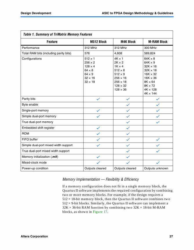
Memory block sizes and configurations are major considerations of SOPC designs, and performance goals determine whether to have device memory on- or off-chip. To satisfy the demand for large memory requirements, Altera FPGAs have a diverse set of memory functions that you can configure for different requirements using the Quartus II software. The Stratix and Stratix GX device families feature TriMatrix™ memory, which can be configured for different memory sizes, as shown in Table 1.
f To learn more about the available memory configurations and features of Stratix and Stratix GX devices, see the Stratix GX FPGA Family Data Sheet and the Stratix Device Family Data Sheet in the Stratix Device Handbook.
Altera Corporation 27Preliminary
Design Development ASIC to FPGA Design Methodology & Guidelines
Memory Implementation — Flexibility & Efficiency
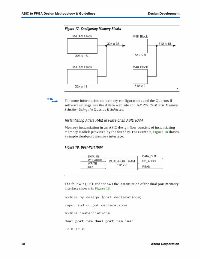
If a memory configuration does not fit in a single memory block, the Quartus II software implements the required configuration by combining two or more memory blocks. For example, if the design requires a 512 × 18-bit memory block, then the Quartus II software combines two 512 × 9-bit blocks. Similarly, the Quartus II software can implement a 32K × 36-bit RAM function by combining two 32K × 18-bit M-RAM blocks, as shown in Figure 17.
Table 1. Summary of TriMatrix Memory Features
Feature M512 Block M4K Block M-RAM Block
Performance 312 MHz 312 MHz 300 MHz
Total RAM bits (including parity bits) 576 4,608 589,824
Configurations 512 × 1256 × 2128 × 464 × 864 × 932 × 1632 × 18
4K × 12K × 21K × 4512 × 8512 × 9256 × 16 256 × 18 128 × 32128 × 36
64K × 864K × 932K × 1632K × 1816K × 3216K × 368K × 648K × 724K × 1284K × 144
Parity bits v v v
Byte enable v v
Single-port memory v v v
Simple dual-port memory v v v
True dual-port memory v v
Embedded shift register v v
ROM v v
FIFO buffer v v v
Simple dual-port mixed width support v v v
True dual-port mixed width support v v
Memory initialization (.mif) v v
Mixed-clock mode v v v
Power-up condition Outputs cleared Outputs cleared Outputs unknown
28 Altera CorporationPreliminary
ASIC to FPGA Design Methodology & Guidelines Design Development
Figure 17. Configuring Memory Blocks
.
f For more information on memory configurations and the Quartus II software settings, see the Altera web site and AN 207: TriMatrix Memory Selection Using the Quartus II Software.
Instantiating Altera RAM in Place of an ASIC RAM
Memory instantiation in an ASIC design flow consists of instantiating memory models provided by the foundry. For example, Figure 18 shows a simple dual-port memory interface.
Figure 18. Dual-Port RAM
The following RTL code shows the instantiation of the dual port memory interface shown in Figure 18.
module my_design (port declarations)
input and output declarations
module instantiations
dual_port_ram dual_port_ram_inst
.clk (clk),
M4K Block
M4K Block
512 × 9
512 × 9
512 × 18
M-RAM Block
M-RAM Block
32k × 18
32k × 18
32k × 36
DUAL-PORT RAM512 × 8
DATA_INWR_ADDRWRITECLK
DATA_OUT
RD_ADDR
READ

Altera Corporation 29Preliminary
Design Development ASIC to FPGA Design Methodology & Guidelines
.data_in (data_in),
.rd_address (rd_address),
.read (read),
.data_out (data_out),
.wr_address (wr_address),
.write (write));
The memory model provided by the ASIC foundry contains timing information for synthesis and a behavioral model for simulation. If the design has to be ported to an Altera FPGA, you must configure the memory requirement from within the Altera MegaWizard Plug-In Manager. The wizard then generates the following set of files.
■ memory.v/memory.vhd This file is a wrapper file that instantiates the Altera library-of-parameterized-modules (LPM) memory module, used for simulation.
■ memory_bb.v/memory_bb.vhd This file is a module declaration used for synthesis.
■ memory_inst.v/memory_inst.vhdThis file is a memory module instantiation example.
Timing information for the memory models, also known as “clear box,” is available in the Quartus II software version 3.0, and can be used with Synplify Pro 7.3 for synthesis. Using these models, Synplify Pro can perform an accurate area and timing estimate.
SimulationAltera provides simulation models of the memory modules generated using the MegaWizard Plug-In Manager for all the device families. Refer to the application notes describing the simulation flow for your choice of a simulator tool.
Synthesis Refer to the application notes describing the synthesis flow for your choice of synthesis tool.
f The Quartus II software Help system provides additional information on Guidelines for Altera Megafunctions & LPM Functions.
Place-and-RouteSimilar to ASIC design flow, the Quartus II software place-and-route tool instantiates the appropriate memory module and performs place-and-route of the design.
f The Quartus II software Help system provides additional information on the instantiation of LPM Megafunctions.

30 Altera CorporationPreliminary
ASIC to FPGA Design Methodology & Guidelines Design Development
1 When designing with Altera FPGAs, you must identify the device during the design planning process, because the available memory resource varies according to the family and device.
The Altera Stratix and Stratix GX device families only support synchronous memory interface. If the design already contains asynchronous references to memory blocks, see AN 210: Converting Memory from Asynchronous to Synchronous for Stratix & Stratix GX Designs.
Design Development Tools
Altera provides you with the following development tools, all of which are available within the Quartus II software.
■ SOPC Builder■ DSP Builder■ MegaWizard Plug-In Manager
You can use these tools to ease SOPC design development, which will reduce time-to-market. The following sections present an overview of these tools, and their advantages.
SOPC Builder
SOPC Builder provides a standardized, graphical environment for creating SOPC designs composed of components including CPUs, memory interfaces, standard peripherals, and user-defined peripherals.
SOPC Builder enables the combination of components such as embedded processors, standard peripherals, IP cores, on-chip memory, interfaces to off-chip memory, and user-defined logic into a custom system module. This tool generates a single system module that instantiates these components, and automatically generates the necessary bus logic to connect them. SOPC Builder also automatically generates Verilog Design Files (.v) and/or VHDL Design Files (.vhd) describing the system, which can be used as a simulation model.
Figure 19 shows an example of a typical set of system components with which SOPC Builder can be used to generate a system-level module in minutes. SOPC Builder will also generate the test bench.

Altera Corporation 31Preliminary
Design Development ASIC to FPGA Design Methodology & Guidelines
Figure 19. Elements of a Typical SOPC Design
Figure 20 shows the SOPC Builder user interface after a set of peripherals are connected to a Nios® processor.
f For more details about the SOPC Builder, refer to documentation at www.altera.com/literature.
Nios Processor
Memory Controller Memory
UARTDMA Controller PCI

32 Altera CorporationPreliminary
ASIC to FPGA Design Methodology & Guidelines Design Development
Figure 20. Altera’s SOPC Builder
DSP Builder
Altera’s DSP Builder integrates the Quartus II software with high-level algorithmic development tools such as MATLAB and Simulink software. The DSP Builder software is a set of building blocks that shortens DSP design cycles by helping designers create the hardware representation of a DSP design in an algorithm-friendly development environment. Figure 21 shows a simple design, built from concept-to-implementation, using the DSP Builder. Several ready-to-use mathematical functions are available within both the MATLAB and Simulink tools, along with simulation models, which can be used to create a schematic. DSP Builder can generate a VHDL description of the design, along with the test bench. DSP Builder also has links to third-party EDA tools, which can be used along with the Quartus II software to perform synthesis, simulation, and place-and-route.

Altera Corporation 33Preliminary
Design Development ASIC to FPGA Design Methodology & Guidelines
Figure 21. DSP Builder Design Flow
The MegaWizard Plug-In Manager
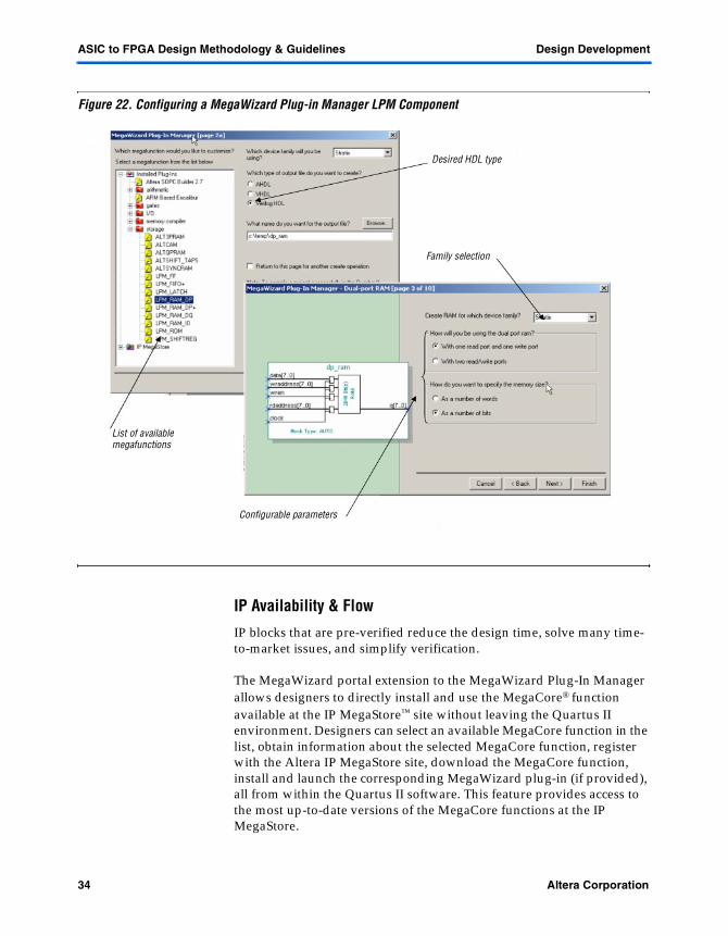
The MegaWizard Plug-In Manager, available in the Quartus II software, helps you create or modify design files that contain custom megafunction variations, which can then be instantiated in a design file. These custom megafunction variations are based on Altera megafunctions, including LPM functions, ranging from simple Boolean gates to complex memory structures.
Figure 22 shows the selections required in the MegaWizard Plug-In Manager to access and edit Altera’s LPM elements.
Drag and drop
Generate VHDL,Synthesize, andplace-and-route
34 Altera CorporationPreliminary
ASIC to FPGA Design Methodology & Guidelines Design Development
Figure 22. Configuring a MegaWizard Plug-in Manager LPM Component
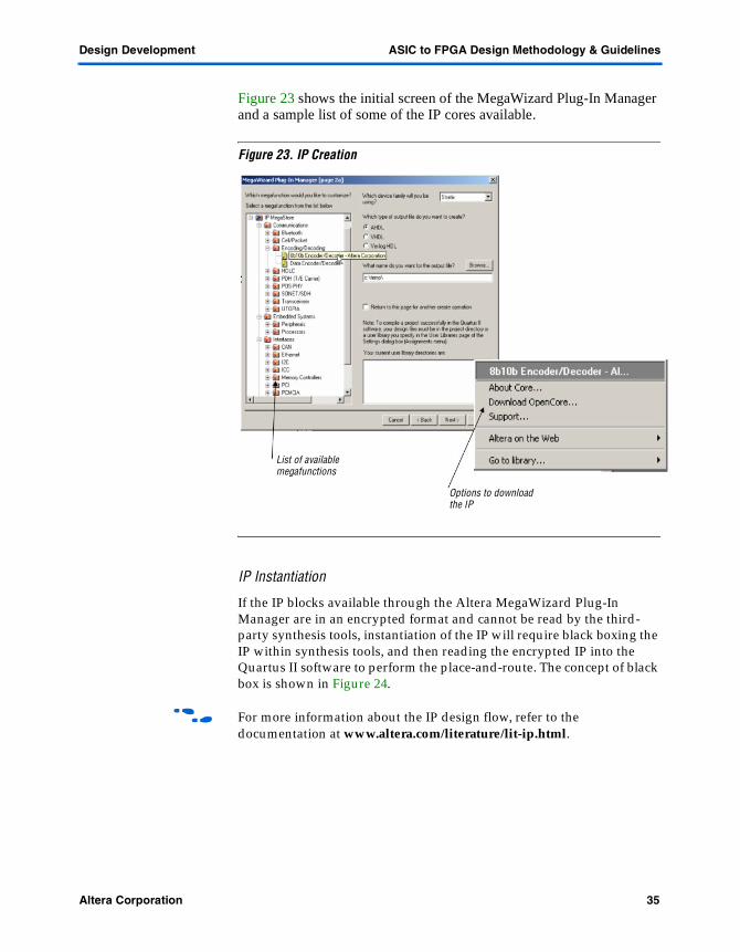
IP Availability & Flow
IP blocks that are pre-verified reduce the design time, solve many time-to-market issues, and simplify verification.
The MegaWizard portal extension to the MegaWizard Plug-In Manager allows designers to directly install and use the MegaCore® function available at the IP MegaStore™ site without leaving the Quartus II environment. Designers can select an available MegaCore function in the list, obtain information about the selected MegaCore function, register with the Altera IP MegaStore site, download the MegaCore function, install and launch the corresponding MegaWizard plug-in (if provided), all from within the Quartus II software. This feature provides access to the most up-to-date versions of the MegaCore functions at the IP MegaStore.
List of availablemegafunctions
Configurable parameters
Family selection
Desired HDL type
Altera Corporation 35Preliminary
Design Development ASIC to FPGA Design Methodology & Guidelines
Figure 23 shows the initial screen of the MegaWizard Plug-In Manager and a sample list of some of the IP cores available.
Figure 23. IP Creation
IP Instantiation
If the IP blocks available through the Altera MegaWizard Plug-In Manager are in an encrypted format and cannot be read by the third-party synthesis tools, instantiation of the IP will require black boxing the IP within synthesis tools, and then reading the encrypted IP into the Quartus II software to perform the place-and-route. The concept of black box is shown in Figure 24.
f For more information about the IP design flow, refer to the documentation at www.altera.com/literature/lit-ip.html.
List of available megafunctions
Options to download the IP

36 Altera CorporationPreliminary
ASIC to FPGA Design Methodology & Guidelines Design Development
Figure 24. IP Instantiation
Functional Simulation
Functional simulation verifies the functionality of the RTL design. The following is the list of supported third-party EDA tools.
■ NC-SIM and Verilog-XL, from Cadence■ VCS and VSS, from Synopsys■ ModelSim®, from Mentor Graphics®
Simulation can also be performed using the Quartus II software native simulator.
Synthesis
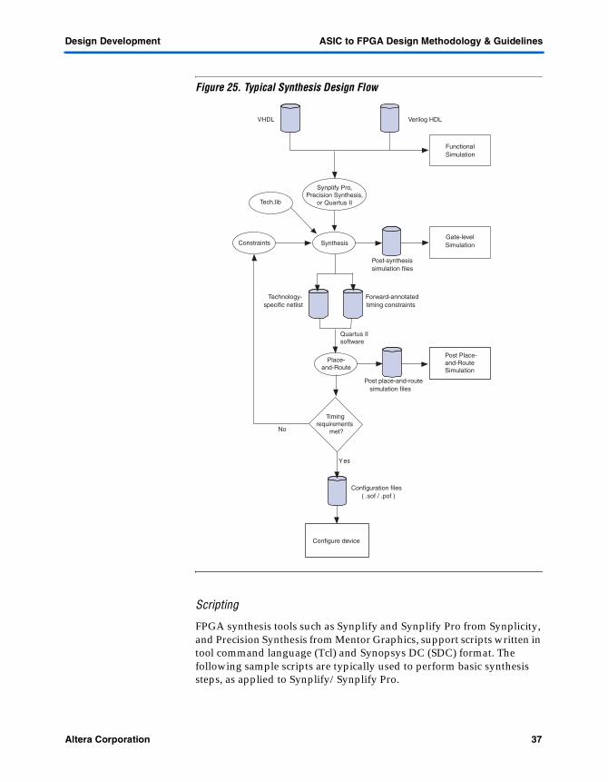
Synthesizing is the process of converting a design representation from RTL code to gate level. Figure 25 shows a typical synthesis flow. Compared to ASIC tools, FPGA synthesis tools are much easier to use in terms of complexity and scripting. Industry-standard FPGA synthesis tools support a limited set of constraints compared to their ASIC counterparts, but the FPGA tools support all of the popular ASIC synthesis techniques, including the following:
■ Top-down or bottom-up approach■ Modular design flow■ Scripting
f For more information on design methodologies, see AN 226: Synplify & Quartus II Design Methodology.
Adder
Counter
Top.v
Filter Black Box
MegaWizard IP Block - FIR Filter
X XX X
Z-1 Z-1Z-1Z-1xinTapped Delay Line
Multipliers by Coefficient
yout
Adder Tree
C-0 C-1 C-2 C-3
Because LPMs are not synthesized by synthesis tools, ‘black-boxing’ is required.
Altera Corporation 37Preliminary
Design Development ASIC to FPGA Design Methodology & Guidelines
Figure 25. Typical Synthesis Design Flow
Scripting
FPGA synthesis tools such as Synplify and Synplify Pro from Synplicity, and Precision Synthesis from Mentor Graphics, support scripts written in tool command language (Tcl) and Synopsys DC (SDC) format. The following sample scripts are typically used to perform basic synthesis steps, as applied to Synplify/Synplify Pro.
Gate-levelSimulation
Post Place- and-Route Simulation
Configure device
Yes
No
Timingrequirements
met?
Constraints
Forward-annotatedtiming constraints
Technology-specific netlist
Post place-and-routesimulation files
Post-synthesissimulation files
Configuration files( .sof / .pof )
Quartus IIsoftware
Synthesis
FunctionalSimulation
VHDL Verilog HDL
Place- and-Route
Synplify Pro, Precision Synthesis,
or Quartus IITech.lib

38 Altera CorporationPreliminary
ASIC to FPGA Design Methodology & Guidelines Design Development
project -new C:/test/fpga_risc8/risc.prj // opens a new project risc.prjadd_file C:/test/fpga_risc8/src/risc8.v // adds the source file to the projectset_option -technology APEX20KE // sets target technology set_option -frequency 50.000000 // sets the speedset_option -num_critical_paths 1 // sets number of critical paths to be reportedset_option -num_startend_points 1 // sets number of start points for the timing reportset_option -pipe 1 // sets the option of pipelining to TRUE set_option -retiming 1 // sets the option of retiming to TRUEadd_file -constraint test.sdc // reads the Synopsys DC style commands from test.sdc project -run synthesis // perform synthesisproject -save C:/test/fpga_risc8/risc.prj // Save the project
SDC ScriptsThe following is a sample of SDC scripts for setting constraints.
define_clock -name {clk} -freq 70.000 -clockgroupdefault_clkgroup //Clock creationdefine_output_delay {dds_out[7:0]} 3.00 -ref clk:r //set output delay with respect to clk //risingdefine_input_delay {expaddr[6:0]} 2.00 -ref clk:f //set input delay with respect to clk //fallingdefine_multicycle_path -from {i:ctl[0]} -to {i:accum[9:0]} 2 //multi cycle path settingdefine_false_path -from {i:ddsstep[7:0]} -to {i:sinout[7:0]} //false path settingdefine_attribute {expread} syn_maxfan {4}// Max fanout attribute setting
Command Line ExecutionThe following is a sample of an SDC script for command line execution.
synplify_pro –batch <file_name>.tcl
f For more information on scripting and supported SDC commands, see the Synplify, or LeonardoSpectrum user and reference manual.

Altera Corporation 39Preliminary
Test Synthesis ASIC to FPGA Design Methodology & Guidelines
Third-Party EDA Tool Support for Synthesis
You can use the following third-party tools to perform synthesis:
■ Synplify Pro and Synplify, from Synplicity■ LeonardoSpectrum and Precision Synthesis, from Mentor Graphics■ FPGA Compiler II, from Synopsys
In addition to the above tools, you can also use the Quartus II software to perform synthesis.
Test Synthesis Vendors test FPGA devices for manufacturing defects, eliminating the need for memory BIST, SCAN insertion, or any other tests typically used to detect manufacturing faults. This completely eliminates the complex task of test synthesis.
Gate-Level Simulation & Timing Analysis
Industry standard EDA tools for simulation can perform gate-level simulation, and a simulation library for all of the Altera FPGA device families is shipped with the Quartus II software.
f For additional detailed information on performing simulation, see the following application notes, available at www.altera.com.
■ AN 239: Using VCS with the Quartus II Software■ AN 204: Using ModelSim-Altera in a Quartus II Design Flow■ AN:197: Using NC-SIM with the Quartus II Software
Altera FPGA design flow also supports PrimeTime from Synopsys to perform static timing analysis, in addition to the timing analysis supported by the Quartus II software. The PrimeTime library for most of the FPGA families is also included with the Quartus II software.
Place-and-Route FPGA design place-and-route is performed using the Quartus II software from Altera. The Quartus II software reads standard EDIF, VHDL, and Verilog HDL netlist files, and generates VHDL and Verilog HDL netlist files, for a convenient interface to other industry-standard EDA tools.
The Quartus II software can perform different types of netlist optimizations to meet performance and area requirements. In addition to netlist optimization, the Quartus II software also supports the LogicLock™ block-based design methodology, and has advanced features to enable fast input/fast output registers to meet the tSU and tCO requirements.
40 Altera CorporationPreliminary
ASIC to FPGA Design Methodology & Guidelines Post Place-and-Route Verification
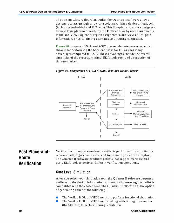
The Timing Closure floorplan within the Quartus II software allows designers to assign logic a row or a column within a device or logic cell (including embedded and I/O cells). This floorplan also allows designers to view logic placement made by the Fitter and/or by user assignments, make-and-view LogicLock region assignments, and view critical path information, physical timing estimates, and routing congestion.
Figure 26 compares FPGA and ASIC place-and-route processes, which shows that performing the back-end tasks for FPGAs has many advantages compared to ASIC. These advantages include the overall simplicity of the process, minimal EDA tools cost, and a reduction of time-to-market.
Figure 26. Comparison of FPGA & ASIC Place-and-Route Process
.
Post Place-and-Route Verification
Verification of the place-and-route netlist is performed to verify timing requirements, logic equivalence, and to estimate power consumption. The Quartus II software produces netlists that support various third-party EDA tools to perform different verification operations.
Gate Level Simulation
After you select your simulation tool, the Quartus II software outputs a netlist with the timing information, automatically ensuring the netlist is compatible with the chosen tool. The Quartus II software has the option of generating either of the following:
■ The Verilog HDL or VHDL netlist to perform functional simulation■ The Verilog HDL or VHDL netlist, along with timing information
(the SDF file) to perform timing simulation
Post - layout Timing Analysis
Routing
Signal Integrity IR drops, Xtalk
Sign off
Sign off
Formal Verification, -
Quartus II Software
Place-and-Route, Re-Synthesis, I/O Placement, Timing
Analysis
FPGA ASIC
Skew and Timing Analysis
Placement and Physical
Optimization
Clock tree synthesis
DRC/ERC, Manual Layout Fixes,
Hold Time Fixes

Altera Corporation 41Preliminary
Post Place-and-Route Verification ASIC to FPGA Design Methodology & Guidelines
Static Timing Analysis
If you select the PrimeTime EDA tool for timing analysis, the Quartus II software will output the Verilog HDL or VHDL gate-level netlist, the SDF file, and the Tcl script to run static timing analysis within PrimeTime. Additionally, PrimeTime libraries are shipped with the Quartus II software.
Formal Verification
The Quartus II software supports formal verification, which uses exhaustive mathematical techniques to verify the design functionality. Within the Altera FPGA design flow, formal verification can be performed between the synthesized and the Quartus II post-fit netlists. Presently, formal verification is only supported for designs synthesized with the Synplify Pro tool.
f For additional information about formal verification support, see AN 296: Using Verplex Conformal LEC for Formal Verification of Design Functionality.
Power Estimation
Altera FPGA design flow supports two methods of power estimation. The first method uses a design utility called the online power calculator. Estimated power consumption can be calculated for various devices based on typical conditions. This online calculator is found in the design utility section of each device family.
f For more information on this calculator, go to www.altera.com/products/ devices/dev-index.jsp.
The Quartus II software also supports the Model Technology™ ModelSim® software to perform a simulation that includes power estimation data. The designer can specify that the Quartus II software should include power estimation data in the Verilog Output File (.vo) or VHDL Output File (.vho) generated for APEX™ 20KE, APEX 20KC, and Mercury™ devices. After simulating the design in the ModelSim software, the ModelSim software uses the power estimation data to generate a Power Input File (.pwf) that can be used within the Quartus II software for estimating the design’s power consumption.
f Additional information on power estimation is available in the Quartus II software Help .

42 Altera CorporationPreliminary
ASIC to FPGA Design Methodology & Guidelines Post Place-and-Route Verification
Clock Tree Synthesis
Clock tree synthesis (CTS) is an important step in the ASIC design methodology, and is performed after placement. CTS builds a clock network to reduce the clock skew between registers in the design. CTS synthesis is either performed by third-party EDA tools that have the capacity to perform physical synthesis, or by the foundry tools. CTS can take a great deal of time, and also may require several iterations before the required clock skew is achieved.
Altera FPGAs have dedicated clock networks that are either global or regional, along with the PLL resources. These clock networks have high drive strength and minimal skew, allowing the FPGA design flow to be free from CTS, resulting in reduced design cycle time. The number of global clock resources available depends upon the family and device, and you must know how many global clock resources are required, and select the device accordingly. Figure 27 shows the Stratix device’s global and regional clock resources.
f To learn more about PLLs and global clock networks, see the appropriate device data sheet.
Figure 27. Stratix Clock Resources
1 Unlike ASIC devices, which can have an almost unlimited number of global clock pins and location choices, FPGA devices have a fixed number of these pins and location choices.
Ensure that the number of clock resources required for the design implementation is equal to, or less than, the global clock and fast clock resources available within an FPGA device. Clock pins are also fixed in location, and design placement should be done to take advantage of the physical location of the clock pin.
CLK[15..12]
CLK[7..4]
CLK[11..8] CLK[3..0]CLK[3..0]
CLK[15..12]

Altera Corporation 43Preliminary
Quartus II Software Features ASIC to FPGA Design Methodology & Guidelines
Quartus II Software Features
The Quartus II software is a fully integrated, architecture-independent package for designing logic with Altera programmable logic devices (PLDs). The Quartus II software offers a full spectrum of logic design capabilities, including the following:
■ LogicLock incremental design ■ Tcl scripts■ SignalTap® II Logic Analyzer ■ SignalProbe™ debugging technology■ Design entry using schematics, block diagrams, AHDL, VHDL, and
Verilog HDL ■ Floorplan editing ■ Powerful logic synthesis including retiming■ Functional and timing simulation ■ Timing analysis ■ Software source file importing, creation, and linking to produce
programming files ■ Device programming and verification
LogicLock
Quartus II software enables a block-based approach using the LogicLock feature. Using this technique, you can independently create and implement each logic module, and integrate all optimized modules into the top-level design. Figure 28 compares traditional design flow with LogicLock design flow.
Figure 28. Comparison Between Traditional & LogicLock Design Flow.
Traditional Design Flow LogicLock Design Flow
Design
Integrate
Optimize
Verify
Design, Optimize, and Verify
Integrate
Verify

44 Altera CorporationPreliminary
ASIC to FPGA Design Methodology & Guidelines Quartus II Software Features
f For additional information on LogicLock methodology and usage, see the following application notes, and the Quartus II Help.
■ AN 161: Using the LogicLock Methodology in the Quartus II Design Software
■ AN 164: LeonardoSpectrum™ and Quartus II LogicLock Design Flow■ AN 165: Synplify and Quartus II LogicLock Design Flow
Register Packing
Register packing combines logic cells that only use the register and logic cells that only use the LUT into a single logic cell to reduce the area, as shown in Figure 29. The following four options are available for register packing.
■ Off: Does not pack registers.■ Normal: Default setting packs registers when this is not expected to
hurt timing.■ Minimize Area: The Quartus II software will aggressively pack
registers to reduce area. The software will not pack registers that are part of a carry-and-cascade chain.
■ Minimize Area with Chains: The Quartus II software will aggressively pack registers, including those that are a component of carry-and-cascade chains, to reduce area. This option is only available for Stratix, Stratix GX, and Cyclone devices.
Figure 29. Register Packing
f For additional information about register packing, see AN 297: Optimizing Performance Using the Quartus II Software and the Quartus II Help.
LUT1 + LUT2 = LUTREGREG2
REG1

Altera Corporation 45Preliminary
Quartus II Software Features ASIC to FPGA Design Methodology & Guidelines
Netlist Optimizations
The Quartus II software includes netlist optimization options to further optimize the design after synthesis and before place-and-route. The option can be applied regardless of the synthesis tool used. Depending on the design, some options may have more of an effect than others. The following three options are available.
■ WYSIWYG primitive re-synthesis■ Gate-level register re-timing■ Logic element duplication
Figure 30 shows each of these options.

46 Altera CorporationPreliminary
ASIC to FPGA Design Methodology & Guidelines Quartus II Software Features
Figure 30. Netlist Optimization Methods
ATOMNetlist
Place&
RouteLE LE
LE
LE
LE
Un-Map
Re-Map
Gate-level Register Re-timing
D Q D Q10 ns D Q 5 ns
D Q D Q7 ns D Q 8 ns
WYSIWYG Primitive Re-synthesis
LE
LE
LE
LELE
LE
LE
LE
LELE
LELE
Logic Element Duplication

Altera Corporation 47Preliminary
Quartus II Software Features ASIC to FPGA Design Methodology & Guidelines
Tcl Scripting
The QuartusII software supports Tcl scripting along with Application Program Interface (API) functions that can be used as Tcl commands. You can generate a Tcl Script File (.tcl) from an existing project created through the Quartus II software, or you can use Tcl language templates and Quartus II Tcl templates to create Tcl scripts.
You can run Tcl scripts or individual Tcl commands from within the Quartus II software and other EDA software tools such as Synplify from Synplicity, and LeonardoSpectrum from Mentor Graphics.
The following Tcl code presents a sample Tcl script to perform basic place-and-route.
# Load Quartus II Tcl Project packagepackage require ::quartus::project
}
# Create and open the projectif {[project_exists test]} {
project_open -cmp clock_sync test} else {
project_new test}
# Project Assignmentsset_global_assignment -name "VQM_FILE" "..\\synplify\\clock_sync.vqm"set_global_assignment -name "COMPILER_SETTINGS" "clock_sync"
# Assign the Synthesis, Simulation and Timing Verification toolsset_global_assignment -name "EDA_SIMULATION_TOOL" -section_id "test" "ModelSim (Verilog HDL output from Quartus II)"set_global_assignment -name "EDA_TIMING_ANALYSIS_TOOL" -section_id "test" "PrimeTime (Verilog HDL output from Quartus II)"
# Input/Output format and reading
set_global_assignment -name "EDA_INPUT_DATA_FORMAT" -section_id "eda_design_synthesis" "EDIF"set_global_assignment -name "EDA_OUTPUT_DATA_FORMAT" -section_id "eda_design_synthesis" "EDIF"
# Device & Family selection
48 Altera CorporationPreliminary
ASIC to FPGA Design Methodology & Guidelines Quartus II Software Features
set_global_assignment -name "FAMILY" "Stratix"set_global_assignment -name "DEVICE" "EP1S40F1508C5"
# Timing Specifications
set_global_assignment -name "FMAX_REQUIREMENT" "40.0 MHz"set_global_assignment -name "TCO_REQUIREMENT" "25ns"set_global_assignment -name "TPD_REQUIREMENT" "25ns"set_global_assignment -name "TSU_REQUIREMENT" "25ns"
# Compile the project and# exit using "qexit" if there is an errorif [catch {qexec "quartus_fit $project_name"} result] {
qexit -error}if [catch {qexec "quartus_tan $project_name"} result] {
qexit -error}
#------ Report Fmax from report ------#set actual_fmax [get_fmax_from_report]puts ""puts "-----------------------------------------------"puts "Required Fmax: $required_fmax Actual Fmax: $actual_fmax"puts "-----------------------------------------------"
#------ Close Project ------#project_close
f For more information on Tcl scripting, see AN 195: Scripting with Tcl in the Quartus II Software and also the Quartus II software Help.
Modular Quartus II Software
With the Quartus II software version 3.0, Altera provides the flexibility of modular executables. Modular executables provide separate programs for each step in an FPGA design flow, from synthesis through simulation and programming. Some benefits of modular executables include reduced memory requirements and improved performance, command-line control over each step of the design flow, easy integration with scripted design flows including Makefiles, and complete compatibility with the easy-to-use Quartus II graphical user interface (GUI) based design flow.

Altera Corporation 49Preliminary
Quartus II Software Features ASIC to FPGA Design Methodology & Guidelines
f To learn more about how to use modular executables, see AN 309: Command-line Scripting in the Quartus II Software.
In-System Verification
In ASIC devices, test points and pins are used to probe various nodes to help identify the source of a problem. With these test points/pins and a logic analyzer, you can effectively determine the source of most problems.
This test method is also used in FPGAs. However, with the re-configurability of FPGAs you have many more advantages. Altera FPGAs support the SignalProbe™ utility, which uses an automated process similar to the points-and-pins method to route internal nodes to unused I/O pins. A logic analyzer can also be used with these SignalProbe pins, similar to the ASIC methodolog. However, since the FPGA is re-configurable, you can embed a SignalTap II logic analyzer into the FPGA itself.
SignalTap II Embedded Logic Analyzer
The SignalTap II embedded logic analyzer captures the data of internal nodes and transfers the data real time, via a download cable, to the Quartus II software to be viewed in a waveform. This embedded logic analyzer supports trigger positions, and trigger events, in the same way that a standard external logic analyzer would.
The SignalTap II logic analyzer allows you to modify the nodes they choose to tap on the fly. This tool also supports various clock domains in your design by instantiating multiple SignalTap II instances into a single device.
Because the SignalTap II logic analyzer uses the programming interface to communicate back to the computer, you do not need extra test pins. Acquired data is saved to the device’s internal RAM and then streamed off-device via the JTAG communication port. This is advantageous when BGA packages are used and access to available pins is difficult, or impossible.
f To learn about the SignalTap II features, see AN 280: Design Verification Using the SignalTap II Embedded Logic Analyzer.

50 Altera CorporationPreliminary
ASIC to FPGA Design Methodology & Guidelines Device Programming (Prototype)
SignalProbe Features
The SignalProbe feature supports incremental routing, allowing designers to quickly route signals to I/O pins for efficient signal verification without affecting the design. When device memory is limited and there is no access to a JTAG communication port, the SignalProbe feature can perform signal debugging and hardware verification.
With the Quartus II software, you can change the selection of nodes that you want routed to pre-specified SignalProbe pins. With these routed SignalProbe pins, you can then use a logic analyzer to analyze your selected internal nodes.
The SignalProbe feature allows you to re-route your signals in as little as 5% of the time required for a full re-compilation. The SignalProbe feature gives quick access to internal design signals to Altera designers for system-level debugging.
f For more information on the SignalProbe feature, refer to the Quartus II Help.
Boundary Scan Description Language (BSDL) Testing
Both ASIC and FPGA devices use BSDL Testing to ensure pin connectivity and functionality. Advances in surface-mount packaging and PC board manufacturing have resulted in smaller boards, making traditional test methods, such as external test probes, harder to implement. BSDL testing can test pin connections without using physical test probes and capture functional data while a device is operating normally.
All Altera devices support BSDL testing. In Altera FPGA devices, a JTAG (TAP) controller is already embedded into the device and does not require any engineering work, unlike ASIC devices. Altera also provides a BSDL file for each device in each family. These BSDL files can be found on the Altera web site.
f For more information about BSDL testing, see AN 39: IEEE 1149.1 (JTAG) Boundary-Scan Testing in Altera Devices.
Device Programming (Prototype)
One difference between ASIC and FPGA devices is that, unlike an FPGA device, functionality of an ASIC device cannot be modified. Once an ASIC device returns from the foundry, the device functionality is fixed and not much can be done to it. Alternatively, FPGA devices can be re-configured many times, providing much more flexibility.

Altera Corporation 51Preliminary
Device Programming (Prototype) ASIC to FPGA Design Methodology & Guidelines
The ability to change the functionality of a device and add enhancements and fixes is common in the prototyping stages. There are various ways FPGA devices can be configured.
Altera SRAM-based FPGA devices (like Stratix, Stratix GX, and Cyclone devices) can be configured in many ways, as shown in Table 2.
Notes to Table 1:(1) The MasterBlaster communications cable uses a standard PC serial or universal serial bus (USB) hardware interface
to download configuration data to APEX II, APEX 20K, Mercury, ACEX 1K, FLEX 10K, and FLEX 6000 devices. It supports operation with VCC at 5.0 V, 3.3 V, 2.5 V, or 1.8 V and is supported by the QuartusTM II software. For more information on the MasterBlaster cable, see the MasterBlaster Serial/USB Communications Cable Data Sheet.
(2) Although you cannot configure FLEX 6000 devices through the JTAG pins, you can perform JTAG boundary-scan testing.
Table 2. Altera SRAM-based Configuration Schemes
Configuration Scheme Device Family Typical USe
Configuration Device APEX II, APEX 20K, Mercury, ACEX 1K, FLEX 10K,
Configuration with the EPC16, EPC8, EPC2, EPC1, or EPC1441 configuration devices.
FLEX 6000 Configuration with EPC1 or EPC1441 configuration devices.
Passive Serial (PS) APEX II, APEX 20K, Mercury, ACEX 1K, FLEX 10K, FLEX 6000
Configuration with a serial synchronous microprocessor interface and the MasterBlasterTM communications cable or ByteBlasterMVTM parallel port download cable. (1)
Passive Parallel Synchronous (PPS)
APEX II, APEX 20K, Mercury, ACEX 1K, FLEX 10K
Configuration with a parallel synchronous microprocessor interface.
Fast Passive Parallel (FPP)
APEX II Configuration with a parallel synchronous configuration device or microprocessor interface where 8 bits of configuration data are loaded on every clock cycle. Eight times faster than PPS.
Passive Parallel Asynchronous (PPA)
APEX II, APEX 20K, Mercury, ACEX 1K, FLEX 10K
Configuration with a parallel asynchronous microprocessor interface. In this scheme, the microprocessor treats the target device as memory.
Passive Serial Asynchronous (PSA)
FLEX 6000 Configuration with a serial asynchronous microprocessor interface.
Joint Test Action Group (JTAG)
APEX II, APEX 20K, Mercury, ACEX 1K, FLEX 10K
Configuration through the IEEE Std. 1149.1 (JTAG) pins. (2)

52 Altera CorporationPreliminary
ASIC to FPGA Design Methodology & Guidelines Device Programming (Prototype)
In general, there are two ways of configuring your FPGA device.
■ Use a download cable■ Use a configuration device
Using a Download Cable
A download cable is used more frequently in the prototyping stages when using SRAM-based FPGA devices. By definition, the prototyping stage will likely require design changes and fixes. In ASIC designs, the device must be removed and replaced by a new ASIC device, or the board is scrapped entirely. With FPGA devices, you can reprogram the device while it is on the board.
The Quartus II software allows you to re-configure your device via a download cable. There are various download cables that can be used to connect to the serial, USB, or parallel port of your computer. You can connect it in a JTAG configuration or in a passive serial configuration.
f For more information, see AN 116: Configuring SRAM-Based LUT Devices.
Using a Configuration Device
SRAM-based FPGA devices must be configured each time the board powers up, and Altera provides various sizes of configuration devices that serve this purpose.
These EEPROM-based configuration devices store the configuration data, and configure the intended device. One typical scenario is to configure your FPGA device with a configuration device passive serially. When the board is powered on, the configuration device(s) will automatically send a serial data stream to the FPGA device and configure it.
Alternatively, you can also store the configuration data in on-board memory and use another PLD (typically an EPROM-based device, or a microprocessor) to act as the controller. When the board is powered on, the controller device will send the configuration data from memory to the targeted FPGA device.
These configuration methods are ideal for the final production boards.
f For more information about the various configuration schemes, see AN116: Configuring SRAM-Based LUT Devices.
Altera Corporation 53Preliminary
Hardcopy Devices ASIC to FPGA Design Methodology & Guidelines
Hardcopy Devices
Altera offers a cost effective ASIC-like alternative to FPGA devices in their HardCopy™ device family. HardCopy devices extend the flexibility of high-density FPGAs to a cost-effective high-volume production solution. The conversion process from an Altera FPGA to a HardCopy device offers seamless migration of a high density system-on-a-programmable-chip to a low-cost alternative device with minimal risk. Using HardCopy devices, Altera’s SOPC solutions can be leveraged from prototype to production, while reducing cost and speeding time-to-market.
A significant benefit of HardCopy devices is that designers do not need to be involved in the device conversion process. Unlike ASIC device development, the HardCopy design does not require generation of test benches, test vectors, or timing and functional simulation. The HardCopy conversion process only requires the Quartus II software-generated output files. Altera performs the conversion and delivers functional prototypes in as few as eight weeks.
f For more information on the HardCopy alternative, see the HardCopy Device Handbook, Volume 1.
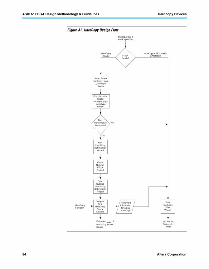
Figure 31 shows the HardCopy design flow after the Quartus II software has generated the .sof file.
54 Altera CorporationPreliminary
ASIC to FPGA Design Methodology & Guidelines Hardcopy Devices
Figure 31. HardCopy Design Flow
Select Stratix hardcopy_fpga
_prototype device
Run HardCopy
Optimization Wizard
Close Quartus FPGA Project
Run HardCopy
Files Wizard
FPGA Family?
Placement Information for Actual HardCopy
Compile to the Stratix
hardcopy_fpga- _prototype
device
Run Performance Estimation?
Start Quartus II HardCopy Flow
HardCopy Stratix
HardCopy APEX 20KE / APEX20KC
Open Quartus
HardCopy Optimization
Project
Compile (to a
HardCopy Stratix Device)
.qar File for Delivery to
Altera
Yes
No
Estimated fMAX of
HardCopy Stratix Device
HardCopy Floorplan

Altera Corporation 55Preliminary
FPGA Financial Benefit ASIC to FPGA Design Methodology & Guidelines
FPGA Financial Benefit
Altera also provides a means of calculating the financial advantages of FPGAs as compared to ASICs. The tool will take inputs parameters and provide an estimate of total projected costs and revenues. This tool is available on the Altera web site.
Conclusion As can be seen by comparing ASIC design flow with FPGA design flow, as shown in Figure 2 on page 3, ASIC design flow consists of more steps compared to those required for FPGAs, and more EDA tools must be used to perform the associated tasks.
ASIC Design Flow Disadvantages
This section lists some of the disadvantages of ASIC design flow compared to FPGA design flow.
■ Initial planning and physical design expertiseASIC design methodology consists of initial physical planning, as follows.
● I/O placement● Memory placement● Power and physical planning
This gives visibility and control of a device’s area and speed early in the design phase. To perform the above tasks, design teams should also have designers with physical design expertise.
■ Test synthesis Scan cells and memory BIST logic adds area and test overhead to detect manufacturing faults.
■ Foundry involvementBack-end tasks involve the physical design planning between the design team and the foundry. Foundry personnel perform place-and-route of the design, and verification and timing analysis is done by the design team. There will be iterations before the final sign-off, resulting in delayed time-to-market.
■ EDA tools Additional number of EDA tools adds to cost and complexity compared to FPGA design flow.
■ NRE chargesDesign re-spin results in increased NRE charges. Also, the masks are extremely expensive, costing approximately $850,000 ������mask manufactured using ����µm �� ������

56 Altera CorporationPreliminary
ASIC to FPGA Design Methodology & Guidelines Conclusion
■ Firmware development Testing of the firmware has to be done after the design fabrication, and any modifications to the firmware results in delayed time-to-market.
■ Time-to-market and high risk Length of the ASIC design cycle is considerably longer compared to FPGA design flow and any modifications to the design results in high NRE charges, and delayed time-to-market.
FPGA Design Flow Advantages
This section lists the advantages of FPGA design methodology.
■ No design-for-test tools neededFPGA devices are free from manufacturing defects, resulting in a scan-free design and eliminating formal verification between the original design and the scan design.
■ Early prototyping and volume production FPGA designs can have a lead time of 10 to 12 weeks compared to ASICs. After a device is chosen, parts can also be ordered well before the design is complete, ensuring they are available as soon as the designer is ready.
■ HardCopyAltera offers the HardCopy family, an ASIC-like alternative to FPGA devices, which is cost effective compared to ASIC.
■ Firmware development Firmware development and testing can be done as soon as the design is prototyped and modifications, either with the firmware or the design, can be accomplished with a short turnaround time.
■ NRE charges and functional flexibilityBecause devices can be re-configured, there is no NRE cost associated with design re-spins, and design modifications are easy to accommodate—taking minutes as compared to months.
■ Place-and-route The Quartus II software from Altera performs place-and-route and generates all the files necessary to build the FPGA, eliminating the requirement of coordinating with an external foundry. The Quartus II software also generates the necessary netlists that can be used with industry-standard simulation and timing verification EDA tools.


58 Altera CorporationPreliminary
101 Innovation DriveSan Jose, CA 95134(408) 544-7000www.altera.comApplications Hotline:(800) 800-EPLDLiterature Services:[email protected]
Copyright © 2003 Altera Corporation. All rights reserved. Altera, The Programmable Solutions Company,the stylized Altera logo, specific device designations, and all other words and logos that are identified astrademarks and/or service marks are, unless noted otherwise, the trademarks and service marks of AlteraCorporation in the U.S. and other countries. All other product or service names are the property of their re-spective holders. Altera products are protected under numerous U.S. and foreign patents and pendingapplications, maskwork rights, and copyrights. Altera warrants performance of its semiconductor productsto current specifications in accordance with Altera's standard warranty, but reserves the right to make chang-es to any products and services at any time without notice. Altera assumes no responsibility or liabilityarising out of the application or use of any information, product, or service describedherein except as expressly agreed to in writing by Altera Corporation. Altera customersare advised to obtain the latest version of device specifications before relying on any pub-lished information and before placing orders for products or services.
Printed on recycled paper
ASIC to FPGA Design Methodology & Guidelines Conclusion


![sqrt(2x-10)+sqrt(3x+10)=sqrt(2x-17)+sqrRadical Equation ...jan.getko.sweb.cz/f6v/Symbolab.pdf · 311 + 3011 21 2111 2] 311 3011 Expand 311 + 311 + — ab + ac 210 ons: a. 311 30 -](https://img.pdfslide.net/doc/110x75/5f935ddb2ac6007d6d2672ec/sqrt2x-10sqrt3x10sqrt2x-17sqrradical-equation-jangetkoswebczf6v.jpg)