Embed Size (px)
Citation preview

IEEE TRANSACTIONS ON CIRCUITS AND SYSTEMS—I: FUNDAMENTAL THEORY AND APPLICATIONS, VOL. 45, NO. 5, MAY 1998 547
An Analytical Solution for a Class ofOscillators, and Its Application to Filter Tuning
Shanthi Pavan,Member, IEEE,and Yannis P. Tsividis,Fellow, IEEE
Abstract—We present a completely analytical solution to afilter–comparator oscillator system, and verify it by macromodelsimulations and experiment. We discuss the applications of thiskind of oscillator in a vector–locked loop system for continuoustime filter tuning. We also apply our solution to the operation ofa resonant switched mode inverter.
Index Terms—Automatic tuning, filter tuning, oscillator, VCO.
I. INTRODUCTION
SINE-WAVE oscillators (Fig. 1) contain an active elementwith sufficient power gain at the oscillation frequency,
a frequency selective network, and an amplitude stabilizingmechanism. They are capable of producing a near-sinusoidalsignal with good phase noise and high spectral purity.
In a sine-wave oscillator, positive feedback is used around afrequency selective circuit to drive the poles of the correspond-ing closed-loop linear system into the right-half s-plane. In thecase to be considered in this paper, the “gain” of the amplifieris set to , as shown in Fig. 2. Such systems are encounteredin nonlinear control systems literature [1]–[3] and have beenused by designers [4], [5] in filter tuning schemes, where oneapproach is to construct an oscillator with filter building blocks(integrators), for the purposes of monitoring and tuning filtercharacteristics. It is important in such schemes to make surethat the filter undergoes no internal limiting phenomena, so thatits response can be predicted by linear system theory. This is incontrast to other oscillator methods, in which limiting withinthe filter can modify the frequency of oscillation [6] of theclosed-loop system, which then does not match and track thelocations of the filter poles with variations in temperature andother environmental factors.
The system of Fig. 2 has been studied earlier in the contextof integrated oscillators using digital blocks. For an analysisof the system using nonlinear differential equations, the readeris referred to [7], where the comparator is realized by usinga cascade of two inverters, and the bandpass filter is anLCR series circuit. The analysis in the above work is doneby approximating the nonlinear transfer characteristic of thecomparator by a suitable transcendental function, and solvingthe nonlinear differential equation obtained using well knowntechniques.
Manuscript received February 10, 1997; revised October 8, 1997. This paperwas recommended by Associate Editor W. Mathis.
S. Pavan is with Texas Instruments Incorporated, Edison, NJ 08837 USA(e-mail: [email protected]).
Y. P. Tsividis is with the Department of Electrical Engineering, ColumbiaUniversity, New York, NY 10027 USA.
Publisher Item Identifier S 1057-7122(98)02532-X.
Fig. 1. Block diagram of an oscillator.
Fig. 2. The filter comparator oscillator.
The filter–comparator system could also be analyzed byusing the describing function approach [2], where the nonlinearblock is replaced by an “equivalent” linear block. A first-orderdescribing function analysis, however, predicts that the systemwill oscillate at the filter pole frequency, regardless of the filterquality factor, which we will see is incorrect. A higher orderdescribing function analysis gets close to the exact result. Anexact method for systems consisting of linear networks andrelays has been proposed by Tsypkin and is described in detailin [2]. This method, however, requires the evaluation of aninfinite series using contour integrals.
The disadvantage of all the above methods for this particularsystem is their complexity. They do not offer much insight intosystem operation, and the solutions are in terms of Fouriercoefficients for the steady-state response. In contrast, thesolution we present in this paper is straightforward, providesintuition, and gives information about all the quantities ofinterest (amplitude, frequency, steady state pulse shape, build-up transient)exactly.
In Section II, we present our method of analysis, using thetransient response, and examine the issue of Total HarmonicDistortion (THD) of the output waveform in considerabledetail. Upper bounds for THD are derived for some relatedtopologies. Section III applies the results of our analysis in theautomatic tuning of continuous time filters. A new vector lockloop approach to filter tuning is presented, along with some
1057–7122/98$10.00 1998 IEEE

548 IEEE TRANSACTIONS ON CIRCUITS AND SYSTEMS—I: FUNDAMENTAL THEORY AND APPLICATIONS, VOL. 45, NO. 5, MAY 1998
Fig. 3. Block diagram of the oscillator.
experimental results. Section IV discusses the applications ofthe presented analysis to switching mode resonant inverters.Section V contains the conclusions of this work.
II. OSCILLATOR TRANSIENT AND STEADY STATE
The system we analyze is shown in Fig. 3. For simplicity,until further notice we assume that the comparator outputlevels are 0 and 1. The filter is of the second-order bandpasstype. Its transfer function is
(1)
In the technique to be proposed below, we will employ thestep response of the filter, , which is
£ £ (2)
or
(3)
where is the unit step function. The step response crosseszero whenever
(4)
or at times
(5)
where
(6)
The mechanism of oscillation buildup will be described withthe aid of Fig. 4. Let us assume that the system is initiallyrelaxed, and that oscillation is triggered by a small positivenoise at the comparator input at time . This willcause a step input to the bandpass filter. The output of
Fig. 4. Oscillation buildup mechanism.
the bandpass filter for will coincide with the filterstep response , as shown in Fig. 4. This waveform crosseszero at , so at that instant the comparator switchesagain. Between this switching instant and the next one, thecomparator output can be represented by the superposition oftwo steps— the first at and the second at :
(7)
Thus, for the same interval, the output of the linear filter canbe obtained using superposition as
(8)
Notice that the zero crossings of are apart fromeach other, just as was the case with . Also, the time atwhich starts coincides with the zero crossingof
. Thus, the output will reach itsnext zero crossing whenboth and cross zero,i.e., at . At this point, the comparator switches again,and so until the next zero crossing, its input will be
(9)
and its output will be
(10)
Reasoning as above, we conclude that the next zero-crossingwill occur at , and so on. It now becomes obviousthat the output of the comparator can be represented for allpositive time by
(11)
PAVAN AND TSIVIDIS: ANALYTICAL SOLUTION FOR A CLASS OF OSCILLATORS 549
Fig. 5. Timing detail.
The filter output then is
(12)
where denotes the integer part of . It is apparentfrom Fig. 4 that the terms in the sum that produces arepositive for if is even, and negativeif is odd. By writing
(13)we see that the terms in the sum are all positive for
, and negative for ,where is an integer. This is shown in Fig. 5.
A. Steady-State Response
The steady-state response can be obtained by using (3) in(12) and allowing to increase. The result of this process, asshown in the Appendix, is
(14)
where
(15)
(16)
(17)
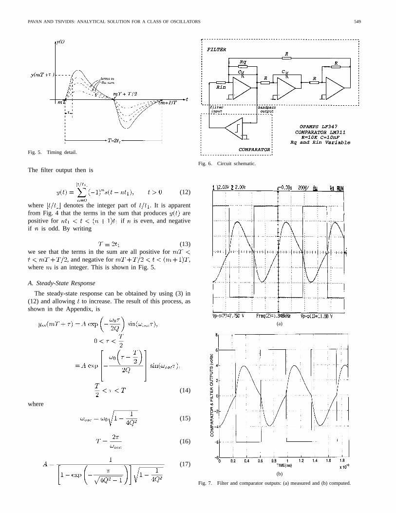
Fig. 6. Circuit schematic.
(a)
(b)
Fig. 7. Filter and comparator outputs: (a) measured and (b) computed.

550 IEEE TRANSACTIONS ON CIRCUITS AND SYSTEMS—I: FUNDAMENTAL THEORY AND APPLICATIONS, VOL. 45, NO. 5, MAY 1998
Fig. 8. Measured (�) and predicted (—) amplitude of oscillation versusQ.
and is any integer. The peak of the oscillatory waveformis obtained by finding the maximum of in thetime interval , and is an exercise in calculus. Wewill find this peak for the special case when the filter qualityfactor is high, using (14) and (17):
(18)
Thus,
(19)
Note that, all along, we have assumed the difference inthe clipping levels of the comparator to be unity. In themore general case, the output will be directly proportionalto the difference in clipping levels of the comparator. Thisproportionality will show itself as a multiplicative constant in(17). If the levels of the comparator are and ( ),then the analysis just presented can still be applied. But now,the step response has to be calculated with nonzero initialconditions. After going through the analysis, it can be shownthat the results (14)–(16) still hold, and that the multiplicativeconstant that must be inserted in (17) is . This comesas no surprise, because the bandpass filter rejects the dccomponent of its input which is nonzero if is notzero.
B. Startup Transient
We now consider the nature of startup dynamics assumingan initially relaxed network. For this analysis, we will focuson the peak of the oscillator output within each half-period.The sequence of peaks can be considered to be a discrete
Fig. 9. Measured (�) and predicted (—) frequency of oscillation versusQ.
Fig. 10. Measured (�) and predicted (—) THD versusQ.
time sequence, and successive peaks can be shown to occurat a time intervals of seconds. We will denote by thepeak of the absolute value of the output in the time interval
. From Fig. 4, (3), (12), and (13), it isevident that we can write
(20)
Since
(21)

PAVAN AND TSIVIDIS: ANALYTICAL SOLUTION FOR A CLASS OF OSCILLATORS 551
Fig. 11. A conventional vector lock loop (VLL).
we obtain
(22)
where
(23)
Note that and the steady-state amplitude, obtainedby setting in (22), is . The time takenfor the output to reach 90% of its steady-state amplitudeis . This is obtained by putting
in (22), solving for , and calculating therequired time as . As expected, as(equivalent to saying that ), the time taken to reachsteady state tends to .
C. Harmonic Distortion Analysis
Based on the detailed analysis of the oscillator steady-statepresented, the steady state response of the filter–comparatorsystem can be obtained by considering an open-loop systemin which the filter is driven by a periodic square wave, offrequency . Expressing this square wave as a Fourierseries, and calculating the attenuation offered to each Fouriercomponent by the filter, it is straightforward [8] to calculatethe spectrum at the output of the filter, and from this the totalharmonic distortion (THD). This result can serve as a usefulbound for THD when the comparator (amplifier) has finitegain. In that case, we assume that the frequency changes onlyvery little from that predicted by the above analysis. So forthe THD estimate, we say that the system is equivalent to afilter driven by an imperfect square wave with finite rise time,and thus with attenuated harmonics in comparison to a perfectsquare wave. It is thus reasonable to assume that THD in thatcase is bounded from above by that in the comparator case.This has been verified by simulations.
D. Experimental Results
We now present experimental results obtained with a bread-boarded prototype of the filter–comparator system. The circuit
(a)
(b)
Fig. 12. (a) � and (b) M surfaces for a conventional VLL (frequencynormalized to reference).
diagram of the system is shown in Fig. 6. The filter sec-tion is a second-order op-amp RC filter, with pole frequen-cies in the low kilohertz range. The comparator used wasLM311(National Semiconductor). As the quality factor waschanged by varying the damping resistor of the biquad, theamplitude and frequency of oscillation changed in extremelygood agreement with theoretical predictions.

552 IEEE TRANSACTIONS ON CIRCUITS AND SYSTEMS—I: FUNDAMENTAL THEORY AND APPLICATIONS, VOL. 45, NO. 5, MAY 1998
(a)
(b)
Fig. 13. Comparison of conventional and proposed technique.
In Fig. 7, we show the predicted and observed waveformsof the comparator and the filter when is one.
The measured and predicted amplitude of the output isshown in Fig. 8. Note that as the quality factor increases, theamplitude increases as predicted by (17). The frequency andtotal harmonic distortion (THD) as a function of filter qualityfactor are shown in Figs. 9 and 10, respectively. Notice that asthe filter gets more selective, the harmonics of the output areattenuated to a greater degree, resulting in a lesser THD. Fromthe figures, it is clear that experimental results agree very wellwith predictions.
III. A PPLICATIONS TO FILTER TUNING
A long-standing problem in filter design has been to tunea filter to a desired response in the face of variations intemperature and other environmental factors, tolerances, andaging. Since tuning (even manual) of a high-order filter iscomplex, integrated tuning schemes have generally relied onmanipulating the response of basic filter building blocks likebiquadratic sections. For a tutorial review of filter tuning, thereader is referred to [9].
The tuning strategy can be indirect [10] or direct [11]. Ineither case, the filter to be tuned is a voltage (or current)controlled filter, that is, a filter whose parameters are “pro-grammable” by a set of control voltages (or currents). For asecond-order section, the parameters of greatest interest are thepole frequency and the pole quality factor. Hence these twoparameters need to be tuned. Implementation of both frequencyand loops is imperative in any high-frequency and/or high-filter design.
The general block diagram of a vector lock loop (VLL)based on a voltage controlled filter (VCF) is shown in Fig. 11[12], [13]. This scheme is chosen in order to appropriately
introduce our proposed scheme in the sequel. The transferfunction of the filter is
(24)
The variable of interest in the frequency control loop is, thephase difference between the reference and the output, whilein the -lock loop, it is , the magnitude of the output atthe pole frequency
(25)
(26)
The above equations show the coupled nature of the phaseand magnitude measurements. To make the coupling effectseven more explicit, the phase and magnitude detector outputsurfaces are drawn in Fig. 12.
We will now point out the problem with interloop couplingin a conventional VLL which uses a second-order filter. Forthis argument, the reader is referred to Fig. 13.
Fig. 13(a) shows the situation with the conventional vectorlocked loop. Assume that, to begin with, the relative shapeof the response is very close to the ideal, while the centerfrequency deviates significantly from the desired value. Forpurposes of argument, assume that frequency andtuningis done sequentially. The magnitude detector will have anoutput which is very low, and this would cause the-loopto increase the filter , although there is only a frequencyerror in the system. Now, however, when the frequency loopconverges to the desired value, the quality factor will be inerror, and the magnitude loop now needs more time to getback to the right value. Notice that if the desired quality factoris large, then even a small error in pole frequency could resultin the magnitude detector sensing a very low output. Thus theproblems with locking tend to get compounded with increasingfilter selectivity. In traditional schemes, these problems aretaken care of by making the -loop much slower than thefrequency loop, so as to make the loops quasi-independent.Note that, ideally, we would want
(27)
(28)
From Fig. 13(a), it is obvious that all the problems with theconventional design could be avoided if we were somehowable to “move” the reference around, so that we can alwayssense the peak gain of the filter, no matter at what frequencyit occurs. This situation is illustrated in Fig. 13(b). Now, the

PAVAN AND TSIVIDIS: ANALYTICAL SOLUTION FOR A CLASS OF OSCILLATORS 553
Fig. 14. Proposed VLL.
magnitude detector output is constant regardless of filter centerfrequency, and a function of quality factor only. To generate a“reference frequency” which is always equal to the filter polefrequency, one can excite the filter and pass its output througha limiter to obtain a constant amplitude. This is precisely whatthe system of Fig. 3 does. From (17), it is apparent that theamplitude of oscillation is now a single-valued function offilter quality factor only, and is completely independent ofpole frequency.
The entire vector lock loop is shown in Fig. 14. Thepole frequency of the filter is set by locking the oscillationfrequency to the reference using a phase-lock loop. The qualityfactor is set by measuring output magnitude. From (15), wesee that the oscillator frequency is an extremely weak functionof . As a numerical example, the difference between theoscillation frequency when changes from 5 to 20 (a changein of 300%) is just 2%. Thus, we can conclude thatthe oscillation frequency is essentially independent offorreasonably high values of . The frequency and amplitudeof oscillation as a function of normalized pole frequency andquality factor are shown in Fig. 15. The independence of mag-nitude and frequency measurements is apparent from these twosurface plots. We now discuss how the scheme just presentedis different from classical VCO methods discussed in theliterature. The classical methods also use the PLL principle andamplitude stabilization, but they focus on single integrators, asopposed to the biquadriatic section in the proposed scheme.The VCO’s implemented in the traditional schemes limitamplitude of oscillation using nonlinear methods, but assumethat the frequency of oscillation remains that of the resonator,which is incorrect. Although the oscillation frequency will beclose to the frequency of the resonator, it will nevertheless bedependent on the nature of the nonlinearity of the amplitudestabilizing element [4], [6]. In indirect tuning methods, thismakes tight tracking between master and slave difficult. Ourscheme operates the filter within its limits of linearity, andcan be used around a resonator with anygreater than 0.5.An alternate solution to keep the filter operating in a linearmode is to use an AGC circuit instead of the comparator
(a)
(b)
Fig. 15. (a) Frequency and (b) amplitude surfaces for proposed VLL (fre-quency normalized to desired pole frequency).
in Fig. 3. Tuning of infinite Q filters by this method hasbeen proposed in [14]–[16]. Note that even in this case, theamplitude and frequency loops are independent [14]. This is

554 IEEE TRANSACTIONS ON CIRCUITS AND SYSTEMS—I: FUNDAMENTAL THEORY AND APPLICATIONS, VOL. 45, NO. 5, MAY 1998
more complicated to implement than the comparator method,and does not offer us the convenience of a square wave output(which is readily available in the comparator case). We nowsummarize the advantages of the VLL just presented.
1) The pole frequency can be tuned with absolutely no errorin spite of offsets in the frequency control loop becausethe system utilizes the PLL principle, in which phaseerrors do not result frequency errors.
2) The reference can be a square wave, unlike in theVCF case, which demands a reference signal with lowharmonic content.
3) The filter operates in a linear fashion, and the oscillationfrequency of the entire system tracks the pole frequencyof the filter with variations in ambient conditions andother environmental factors.
4) The amplitude and frequency loops are independent.5) This can be used in direct tuning schemes, because
the filter to be used can be tuned directly in contrastto conventional VCO schemes which tune individualintegrators.
Thus, this loop is a marriage of the VCF and the PLLschemes, combining the advantages of both in the samemethod, and getting rid of the disadvantages of either methods.The loop has the same circuit complexity as any other VLLscheme.
A. Experimental Results
A low-frequency version of the proposed (VLL) was bread-boarded. The master–slave system was realized by using MOStransistor arrays. The filter topology was a second-order filterof the Tow–Thomas kind, with tunable pole frequency andquality factor. The comparator used was an LM311 (NationalSemiconductor Corp.). The pole frequency and quality factorof the filter were observed to adjust to the reference frequencyand the dc voltage reference to the magnitude locked loop.Setting these quantities, filter tuning could be accomplishedfor reference frequencies of 1.4–2.7 kHz, andvalues from1–6. No special steps were adopted for stabilizing the loops,and we encountered no problems with stability of either loop.The limited capture and lock ranges of the PLL were due to thefact that no attempt was made to optimize the design, whichwas done just to check functionality of the VLL. Fig. 16 showsthe functionality of the frequency and loops.
IV. A PPLICATIONS TO SWITCHED
MODE RESONANT OSCILLATORS
Switched mode resonant oscillators form a useful classof systems, finding application in dc to ac conversion. Theschematic of a switching mode resonant dc-to-ac inverter isshown in Fig. 17. If the voltage across the series LCR networkis written as , note that the current can be written as
(29)
The polarity of the voltage source switched across the circuitis dependent on the zero crossings of the current. Notice thatthe current is a bandpass-filtered version of the voltage, and
(a)
(b)
Fig. 16. Functionality testing of the proposed VLL: (a) varying centerfrequency by varying frequency reference and (b) varying quality factor byvarying voltage reference.
Fig. 17. A switching mode resonant dc-to-ac converter.
hence the system is exactly equivalent to the system shownin Fig. 2. Hence, the analysis we have presented holds in itsentirety. In this case
(30)
(31)

PAVAN AND TSIVIDIS: ANALYTICAL SOLUTION FOR A CLASS OF OSCILLATORS 555
The behavior of this system has been investigated bynumerical simulation in [17] and [18]. The conclusion reachedin the references is the same—the minimumrequired foroscillation is 1/2. The references cited above also investigatethe behavior of this oscillator at the edge of oscillation, thatis, at a of around the above critical value.
V. CONCLUSIONS
In this paper, we have presented an analytical technique forthe solution of a class of sinusoidal oscillators. A vector lockloop, based on this class, has been proposed. The individualloops of this VLL are uncoupled. This scheme combines thebest of both the VCF and VCO schemes. We also discussedthe applications of our solution to resonant switched modeinverters.
APPENDIX
For this analysis, the reader is referred to Fig. 5. We usefrom (13), and denote by the even integer .
Then, from (12), we get
(32)
Using a change of variables, and keeping in mind thatiseven, for , (29) can be written as follows:
(33)
In order to avoid unwieldy expressions, and in preparation forthe development that follows, we use the notation
(34)
Equation (3) for becomes, using (6) and (31),
(35)
Using (32) in (30), and noting that, we get
(36)
or, using (6),
(37)
To calculate the steady-state response, we allowto increase.In the limit, replacing the sum by an infinite sum, and using
(38)
the right hand side of (34) becomes
(39)
It is obvious from Fig. 4 that for , the steady-state response shape is the same as in the interval ,except for a sign inversion. Thus, (14)–(17) in Section II hold,where is as in (13).
ACKNOWLEDGMENT
The authors sincerely thank K. Nagendra for the bread-board implementation of the VLL. They also wish to thankthe anonymous reviewers for their suggestions.
REFERENCES
[1] T. E. Stern,Theory of Nonlinear Networks and Systems.Reading, MA:Addison-Wesley, 1965.
[2] A. Gelb and V. Velde,Multiple-Input Describing Functions and Nonlin-ear System Design.New York: McGraw-Hill, 1968.
[3] Y. Z. Tsypkin, Relay Automatic Systems.Moscow, Russia: Nauka,1974.
[4] J. M. Khoury, “Design of a 15 MHz CMOS continuous-time filter withon-chip tuning,”IEEE J. Solid State Circuits,vol. SC-26, pp. 1988–1997,Dec. 1991.
[5] D. R. Welland, S. M. Phillip, K. Y. Leung, G. T. Tuttle, S. T. Dupuie, D.R. Holberg, R. V. Jack, N. S. Sooch, K. D. Anderson, A. J. Armstrong,R. T. Behrens, W. G. Bliss, T. O. Dudley, W. R. Foland, N. Glover,and L. King, “A digital read–write channel with EEPR4 detection,” inIEEE Int. Solid State Circuits Conf. Dig., 1994, pp. 276–277.
[6] R. F. Adams and D. O. Pederson, “Non-linear contribution to oscillation-frequency sensitivity inRC integrated oscillators,”IEEE J. Solid StateCircuits, vol. SC-6, pp. 406–412, Dec. 1971.
[7] M. Murata, M. Ohta, K. Suzuki, and T. Namekawa, “Analysis of anoscillator consisting of digital circuits,”IEEE J. Solid State Circuits,vol. SC-5, pp. 165–168, Aug. 1970.
[8] K. Clarke and D. Hess,Communication Circuits: Analysis and Design.Reading, MA: Addison-Wesley, 1971.
[9] R. Schaumann and M. A. Tan, “The problem of on-chip automatic tuningin continuous time integrated filters,” inIEEE Proc. ISCAS,1989, pp.106–109.
[10] K. R. Rao, V. Sethuraman, and P. K. Neelakantan, “Novel follow-the-master filter,”Proc. IEEE,vol. 63, pp. 1725–1726, Dec. 1977.
[11] Y. Tsividis, “Self-tuned filters,”Electron. Lett.,vol. 17, no. 12, pp.406–407, June 1981.
[12] D. Senderowicz, D. A. Hodges, and P. R. Gray, “An NMOS inte-grated vector-locked loop,” inProc. IEEE Int. Symp. CAS,1982, pp.1164–1167.
[13] V. Gopinathan, Y. Tsividis, K.-S. Tan, and R. K. Hester, “Design consid-erations for high-frequency continuous-time filters and implementationof an anti-aliasing filter for digital video,”IEEE J. Solid State Circuits,vol. SC-25, pp. 1368–1378, Dec. 1990.
[14] J. O. Voorman, “On balanced gyrator filters,” inIntegrated ContinuousTime Filters—Design and Applications.New York: IEEE Press, 1991,p. 83.
[15] V. Gopinathan, “High frequency transconductance—Capacitancecontinuous-time filters,” Ph.D. dissertation, Columbia Univ., New York,NY, 1990.
[16] J. M. Khoury, “Notes on continuous time filters,” Mead Electronics,1995.

556 IEEE TRANSACTIONS ON CIRCUITS AND SYSTEMS—I: FUNDAMENTAL THEORY AND APPLICATIONS, VOL. 45, NO. 5, MAY 1998
[17] B. Z. Kaplan and R. Rabinovici, “Autonomous switching mode resonantinverter as a limit cycle oscillator in disguise,”Int. J. Syst. Sci.,vol. 24,no. 11, pp. 2199–2203, 1993.
[18] B. Z. Kaplan and D. Guetta, “Switching mode limit-cycle resonantoscillator as a relaxation oscillator,”J. Franklin Inst., vol. 333B, no.6, pp. 833–847, 1996.
Shanthi Pavan (M’98) was born in Narasaraopet,India, in 1973. He received the B.Tech. degree inelectronics and communications engineering fromthe Indian Institute of Technology, Madras, in 1995,and the M.S. degree in electrical engineering fromColumbia University, New York, in 1997.
He is now with the Circuit Techniques Labora-tory, Texas Instruments, Edison, NJ. His researchinterests are continuous time filters and high-speedcircuits for hard disk drive systems.
Yannis P. Tsividis (S’71–M’74–SM’81–F’86) re-ceived the B.S. degree from the University of Min-nesota, Minneapolis, and the M.S. and Ph.D. degreesfrom the University of California, Berkeley.
He is with the Department of Electrical Engineer-ing, Columbia University, New York, as a Professorand Director of the Microelectronic Circuits andSystems Laboratory. He has worked for MotorolaSemiconductor and AT&T Bell Laboratories, andhas taught at the University of California, Berke-ley, MIT, and the National Technical University of
Athens.Dr. Tsividis is the recipient of the 1984 IEEE Baker Best Paper Award
and the 1986 European Solid-State Circuits Conference Best Paper Award.He is co-recipient of the 1987 IEEE Circuits and Systems Society DarlingtonBest Paper Award. He has received the Great Teacher Award at ColumbiaUniversity.


![Tuning Fork Analytical Balance HT/HTR Seriesvibra.co.jp/global/pdf/manual/HT-HTR/270002M11_HT[R]-E_E.pdf270002M11 Tuning Fork Analytical Balance HT/HTR Series Operation Manual To ensure](https://img.pdfslide.net/doc/110x75/5afb761b7f8b9a4465905b74/tuning-fork-analytical-balance-hthtr-r-eepdf270002m11-tuning-fork-analytical.jpg)