Embed Size (px)
Citation preview
An Electrochemical Amperometric
Sensing Circuit with Wireless Interface
for Detection of Neural Signals
� Amanpreet Singh
� Abhilash Goyal
� Saravanan TK
� Gopal B. Iyer
Contents
1. Introduction .................................................................................................................................... 4
2. System Block Diagram...................................................................................................................... 4
3. System level simulation ................................................................................................................... 5
A) Detailed System Simulations in Matlab ........................................................................................ 5
B) Detailed System Simulations in Cadence ...................................................................................... 8
4. Integrator ...................................................................................................................................... 10
a) Op-amp implementation 1- Folded Cascode architecture ........................................................... 11
b) Op-amp Implementation 2 – Sub-threshold Operation ............................................................... 14
5. Comparator ................................................................................................................................... 19
6. Manchester Encoder ...................................................................................................................... 25
7. FSK Modulator ............................................................................................................................... 29
8. RF - Output Buffer and Differential-to-Single Ended Conversion ..................................................... 31
9. Test Signal Generator .................................................................................................................... 33
10. Current Reference Generator ..................................................................................................... 35
11. Bandgap Voltage Reference ....................................................................................................... 37
12. Project Timeline ......................................................................................................................... 41
a) Proposed Timeline ..................................................................................................................... 41
b) Proposed Deadlines ................................................................................................................... 41
c) Progress Report ......................................................................................................................... 41
13. References ................................................................................................................................. 42
List of figures
Figure 1: Neural Sensor Interface lineup .................................................................................................. 5
Figure 2: Simulink model of the ADC ........................................................................................................ 5
Figure 3: Digitized Output signal versus Input signal ................................................................................ 6
Figure 4: Filtered Output Waveform v/s the Input Signal ......................................................................... 7
Figure 5: Schematic level model of the Delta-Sigma ADC ......................................................................... 8
Figure 6: ADC Output v/s Input Current ................................................................................................... 9
Figure 7: Input Current and Integrated Output of the Sigma-Delta ADC ................................................... 9
Figure 8: Block diagram for the Integrator ............................................................................................. 10
Figure 9: Op-amp implementation 1 schematic ..................................................................................... 11
Figure 10: Bode Plots for Op-amp1 ........................................................................................................ 12
Figure 11: Output noise for Op-amp1 .................................................................................................... 13
Figure 12: Op-amp1 connected as an Integrator .................................................................................... 14
Figure 13: Op-amp Implementation 2 Schematic ................................................................................... 15
Figure 14: Bode Plot for Om-amp2 ........................................................................................................ 16
Figure 15: Output noise for Op-amp2 .................................................................................................... 17
Figure 16: Op-amp2 as an Integrator ..................................................................................................... 18
Figure 17: Comparator Implementation 1 .............................................................................................. 19
Figure 18: Self-biased Differential Amplifier for Comparator 1 ............................................................... 20

Figure 19: Waveforms for Comparator 1 ................................................................................................ 21
Figure 20: Comparator Implementation 2 - Cascaded stages .................................................................. 22
Figure 21: Comparator 2 Stage 1............................................................................................................ 23
Figure 22: Comparator 2 Stage 2............................................................................................................ 24
Figure 23: Comparator 2 Output Waveforms ......................................................................................... 25
Figure 24: Manchester Encoding............................................................................................................ 26
Figure 25: Manchester Encoder Schematic ............................................................................................ 26
Figure 26: Timing diagram for our Manchester Encoder......................................................................... 27
Figure 27: Basic components of a typical RF Manchester data receiver system ...................................... 27
Figure 28: Simple data-slicer circuit for restoring binary logic levels ....................................................... 28
Figure 29: Low-level Manchester data stream input is data-sliced to a logic level output ....................... 28
Figure 30: Block diagram of the Transmitter lineup ................................................................................ 29
Figure 31: Circuit diagram of the VCO .................................................................................................... 29
Figure 32: Input and Output signal from the VCO................................................................................... 30
Figure 33: Output signal for '1' and plot of Frequency variation ............................................................. 30
Figure 34: Output signal for '0' and plot of Frequency Variation............................................................. 31
Figure 35: Schematic of Single stage of Buffer ....................................................................................... 31
Figure 36: Output of Buffer and Frequency Variation plot ...................................................................... 32
Figure 37: Schematic of Differential Amplifier ........................................................................................ 32
Figure 38: Output of Differential to Single Ended Converter and Frequency Variation plot..................... 33
Figure 39: Schematic of the Test-Signal Generator ................................................................................. 34
Figure 40: Conceptual Waveform of the Test Signal ............................................................................... 34
Figure 41: A self-biased Bandgap Voltage based Current Reference ....................................................... 35
Figure 42: Temperature characteristic of the Current Reference ............................................................ 36
Figure 43: BGR Implementation 1 .......................................................................................................... 37

Figure 44: Vref v/s Temperature for BGR1 ............................................................................................. 38
Figure 45: BGR Implementation 2 .......................................................................................................... 39
Figure 46: Error Amplifier for BGR2 ....................................................................................................... 39
Figure 47: Noise and temperature variation curves for BGR2 ................................................................. 40
1. Introduction
The etiology of neurological diseases, like epilepsy and stroke, require real-time and sensitive
detection and monitoring of neurotransmitters. Neurotransmitters are molecular messengers across the
electrically insulating synaptic gaps between neurons. Electrochemical detection is the preferred means
of neurotransmitter measurement due to its high sensitivity, its fast detection speed and its ability to
perform distributed measurement.
Neurotransmitters are chemicals which relay, amplify and modulate signals between a neuron and
another cell. They get released into the synaptic cleft, where they bind to receptors in the membrane on
the side of the synapse. The release of neurotransmitters usually follows arrival of an action potential at
the synapse, but may follow graded electrical potentials. Low level “baseline” release also occurs
without electrical stimulation.
Shortcomings of the traditional neural-recording methods like power consumption, size and
physical restraint of the subject by tethering to the monitoring equipment have been addressed with
CMOS integration. We present a CMOS Wireless Neuro-Transmitter IC that is a single chip solution for
neural measurement in vivo.
2. System Block Diagram
The complete neural sensor system schematic is given below. The test signal generator consists
of a counter and current mirror to generate pA range of current. The Analog sensor front end consists of
a Current steering DAC and a Sigma delta modulator whose output feeds to the RF Transmitter. The
input block of the transmitter is a Manchester Encoder which generates a digital signal to control the
VCO’s output frequency to generate a Binary FSK. This signal is buffered and converted from Differential
to Single-Ended before transmission. The clock required for latch and comparator is obtained from an
external source. The chip features a clock divider network which generates the non-overlapping clock as
per the requirements. We are exploring the option to generate the clock on-chip using a Ring-Oscillator.
That way, we minimize the signals that need to be fed in externally.

Figure 1: Neural Sensor Interface lineup
3. System level simulation
A) Detailed System Simulations in Matlab
The Matlab model proves at a conceptual level that Ultra-low level current sensing is achievable
by using delta-sigma based current sensing. This modeling exercise helps in understanding the
interaction between the various elements in the analog frontend loop and the sensitivity to various
parametric variations in the circuit. System noise is also modeled in order to correlate the noise
performance of the current sensing DAC and integrator circuits. The Matlab model is shown in fig1
below:
Figure 2: Simulink model of the ADC
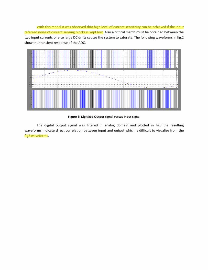
With this model it was observed that high level of current sensitivity can be achieved if the input
referred noise of current sensing blocks is kept low. Also a critical match must be obtained between the
two input currents or else large DC drifts causes the system to saturate. The following waveforms in fig.2
show the transient response of the ADC.
Figure 3: Digitized Output signal versus Input signal
The digital output signal was filtered in analog domain and plotted in fig3 the resulting
waveforms indicate direct correlation between input and output which is difficult to visualize from the
fig2 waveforms.
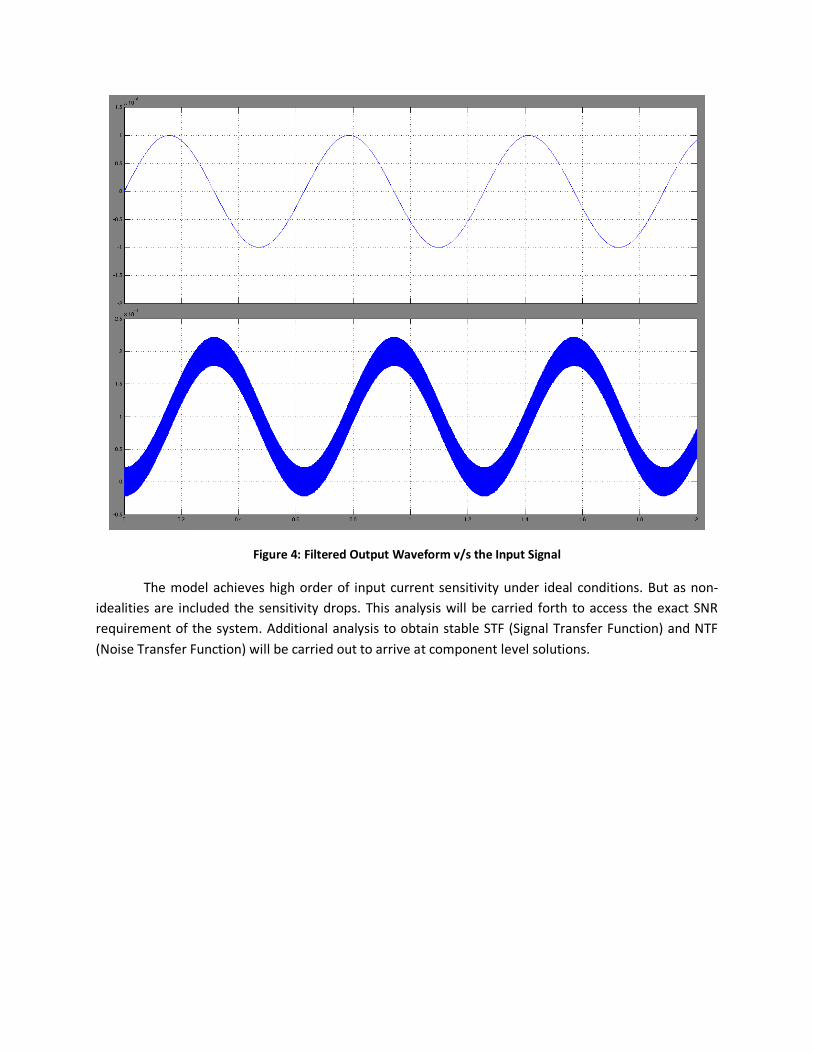
Figure 4: Filtered Output Waveform v/s the Input Signal
The model achieves high order of input current sensitivity under ideal conditions. But as non-
idealities are included the sensitivity drops. This analysis will be carried forth to access the exact SNR
requirement of the system. Additional analysis to obtain stable STF (Signal Transfer Function) and NTF
(Noise Transfer Function) will be carried out to arrive at component level solutions.
B) Detailed System Simulations in Cadence
The Matlab model is designed using Simulink acts as precursor to circuit level modeling. This
helped in developing an insight into the transient behavior of the delta-sigma ADC. There is still a high
level of complexity involved in each circuit element which needs to be analyzed to understand the
performance bottlenecks and design issues in the current process technology. This exercise is required
to validate block level circuit specifications and performance objectives. The cadence circuit level model
was a created using a few ideal components while circuits level design of these blocks were carried out
in tandem. The schematic of the circuit level model is shown in fig4 below:
Figure 5: Schematic level model of the Delta-Sigma ADC
It was with this model, we unraveled that the current sensing circuit is especially sensitive to any
coupled noise. The switching at the gates of the current steering D to A converter can lead to large
deviations in the integrator output which desensitizes the loop. The object is to replace each ideal
element in the loop one at a time and still retain the functionality. The ADC output is shown in fig5
below where we can see a agreement between the Matlab model and schematic level design, although
the waveform show significant deterioration from the Matlab output. The model currently lacks the
calibration block which is required to meet the current sensitivity range. We also indent to model a test
structure (Ultra low current generation circuit) for self testing of the system.
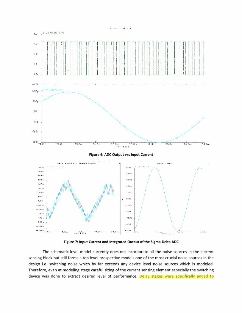
Figure 6: ADC Output v/s Input Current
Figure 7: Input Current and Integrated Output of the Sigma-Delta ADC
The schematic level model currently does not incorporate all the noise sources in the current
sensing block but still forms a top level prospective models one of the most crucial noise sources in the
design i.e. switching noise which by far exceeds any device level noise sources which is modeled.
Therefore, even at modeling stage careful sizing of the current sensing element especially the switching
device was done to extract desired level of performance. Delay stages were specifically added to
drastically reduce the slew rate of the switching pulses to avoid unwarranted interference and we can
see that at this stage a sensitivity of nearly 500pA was achieved. This model will serve as integration
test-bed for the ADC and different block owners can analyze the impact of their block performance on
overall system. This will also be used to complete the RF line-up required for data transmission.
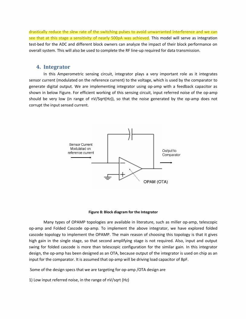
4. Integrator
In this Amperometric sensing circuit, integrator plays a very important role as it integrates
sensor current (modulated on the reference current) to the voltage, which is used by the comparator to
generate digital output. We are implementing integrator using op-amp with a feedback capacitor as
shown in below Figure. For efficient working of this sensing circuit, input referred noise of the op-amp
should be very low (in range of nV/Sqrt(Hz)), so that the noise generated by the op-amp does not
corrupt the input sensed current.
Figure 8: Block diagram for the Integrator
Many types of OPAMP topologies are available in literature, such as miller op-amp, telescopic
op-amp and Folded Cascode op-amp. To implement the above integrator, we have explored folded
cascode topology to implement the OPAMP. The main reason of choosing this topology is that it gives
high gain in the single stage, so that second amplifying stage is not required. Also, input and output
swing for folded cascode is more than telescopic configuration for the similar gain. In this integrator
design, the op-amp has been designed as an OTA, because output of the integrator is used on chip as an
input for the comparator. It is assumed that op-amp will be driving load capacitor of 8pF.
Some of the design specs that we are targeting for op-amp /OTA design are
1) Low input referred noise, in the range of nV/sqrt (Hz)

2) High gain of the order of 70dB
3) Power consumption as low as possible
Two op-amps have been implemented. Design 1 works in saturation region and Design 2 works in the
subthreshold regime (weak-inversion).
a) Op-amp implementation 1- Folded Cascode architecture
In this design, folded cascode is implemented in as shown in figure below. The input stage is N-
MOS differential pair and output is obtained at folded output stage. The results are summarized in Table
below. The total current consumption for op-amp with biasing circuit is 30µA and input referred noise
@100Hz is 32nV/(sqrt(Hz). The simulation results are shown below. These simulations are obtained for
TT corner case.
Figure 9: Op-amp implementation 1 schematic
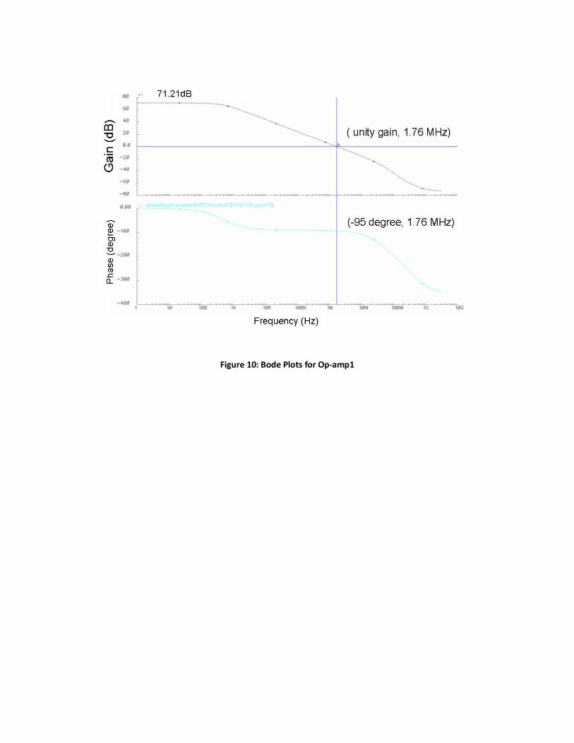
Figure 10: Bode Plots for Op-amp1
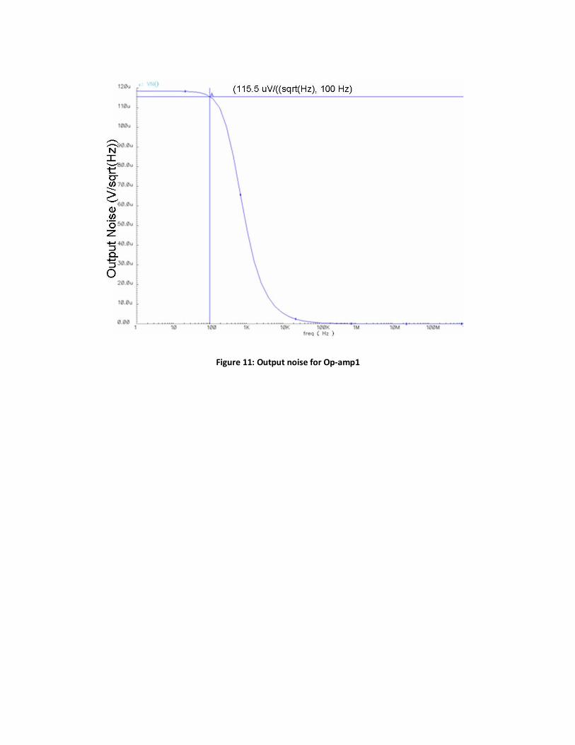
Figure 11: Output noise for Op-amp1
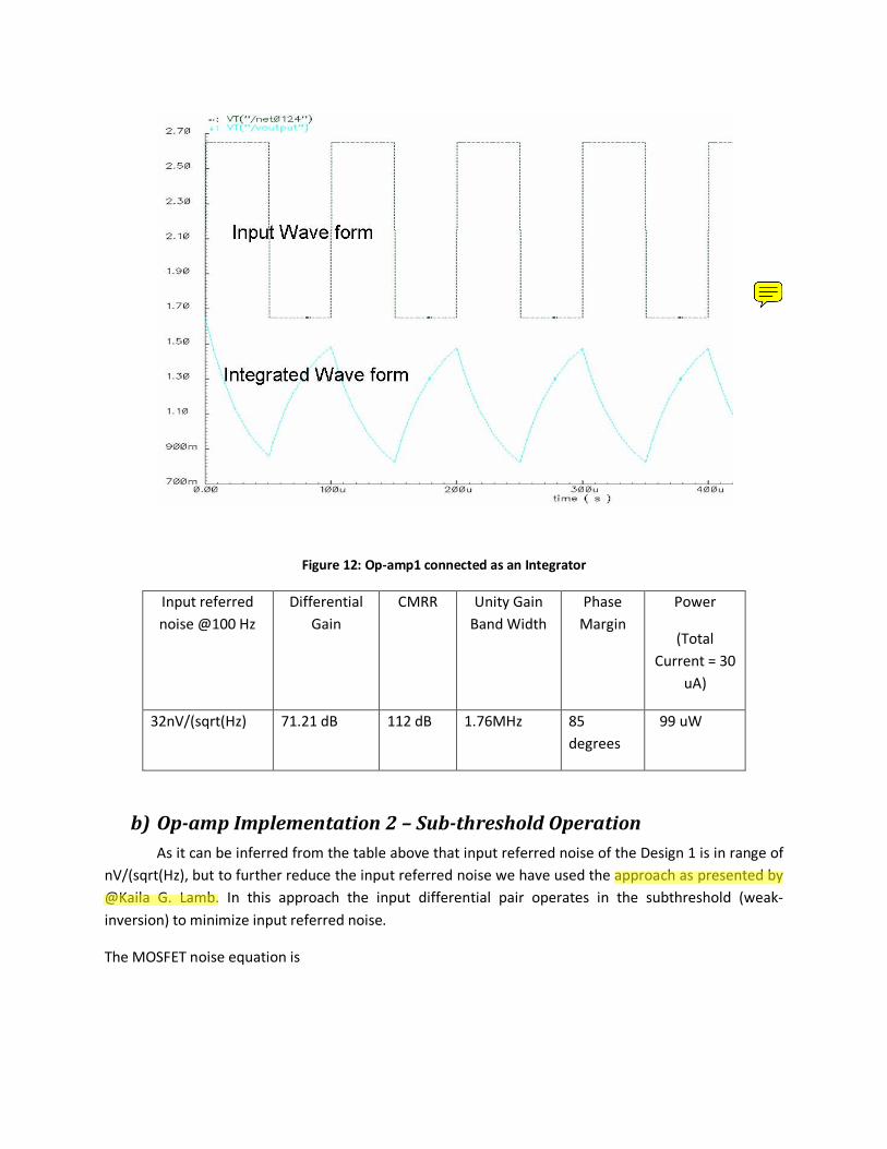
Figure 12: Op-amp1 connected as an Integrator
Input referred
noise @100 Hz
Differential
Gain
CMRR Unity Gain
Band Width
Phase
Margin
Power
(Total
Current = 30
uA)
32nV/(sqrt(Hz) 71.21 dB 112 dB 1.76MHz 85
degrees
99 uW
b) Op-amp Implementation 2 – Sub-threshold Operation
As it can be inferred from the table above that input referred noise of the Design 1 is in range of
nV/(sqrt(Hz), but to further reduce the input referred noise we have used the approach as presented by
@Kaila G. Lamb. In this approach the input differential pair operates in the subthreshold (weak-
inversion) to minimize input referred noise.
The MOSFET noise equation is

As seen from this equation, white noise (the first term) is inversely proportional to the
transconductance; thus, increasing transconductance will result in less white noise. Since gm in
subthreshold is given by below equation, the transconductance to the drain current ratio for a MOSFET
is maximized in subthreshold operation, thus giving good noise performance.
In this design approach, the input devices have width-to-length (W/L) is increased to insure that
input pair operate in substhresold (weak-inversion) for the same bais current. The obtained results are
summarized in Table xx. The input referred noise for this design at @100 Hz is 22 nV/sqrt(Hz), which is
less than the input referred noise of Design 1.
Figure 13: Op-amp Implementation 2 Schematic

Figure 14: Bode Plot for Om-amp2
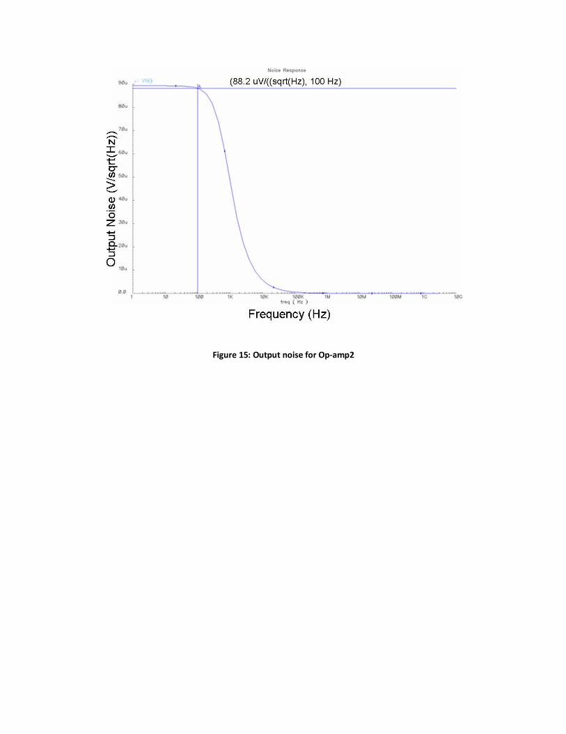
Figure 15: Output noise for Op-amp2
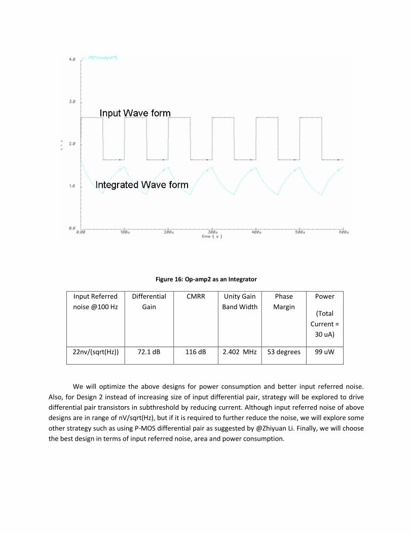
Figure 16: Op-amp2 as an Integrator
Input Referred
noise @100 Hz
Differential
Gain
CMRR Unity Gain
Band Width
Phase
Margin
Power
(Total
Current =
30 uA)
22nv/(sqrt(Hz)) 72.1 dB 116 dB 2.402 MHz 53 degrees 99 uW
We will optimize the above designs for power consumption and better input referred noise.
Also, for Design 2 instead of increasing size of input differential pair, strategy will be explored to drive
differential pair transistors in subthreshold by reducing current. Although input referred noise of above
designs are in range of nV/sqrt(Hz), but if it is required to further reduce the noise, we will explore some
other strategy such as using P-MOS differential pair as suggested by @Zhiyuan Li. Finally, we will choose
the best design in terms of input referred noise, area and power consumption.

5. Comparator
The comparator is a key block in the delta-sigma loop. We are exploring the clocked
comparator for conserving power. However switching introduces kickback noise that can find its way
back to the sensor. In which case, the non-clocked open-loop implementation would perform better.
Both approaches are being explored simultaneously. Here are the out findings:
One of the comparator versions that we are currently trying to optimize is presented below.
This is the simple open loop version with a D Flip-Flop latch at the output (not shown). The static power
consumption was found to be 725µW with a 3.3V supply at the nominal process corner. The self-biased
differential amplifier section has been designed to provide a complete rail to rail operation. The
comparator signal can now be sent to the RF transmitter section after digital encoding.
Comparator
type
Vin IDC PDISS FCLK FIN
Cross-coupled
clocked (Sense
Amp type)
±100mV over
1.6V DC
219.7µA 725.1µW 10MHz 100KHz
Figure 17: Comparator Implementation 1
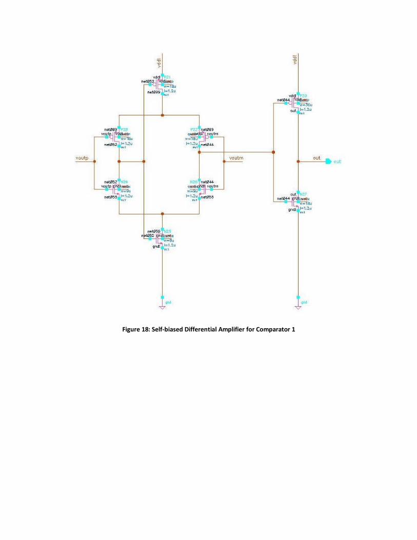
Figure 18: Self-biased Differential Amplifier for Comparator 1
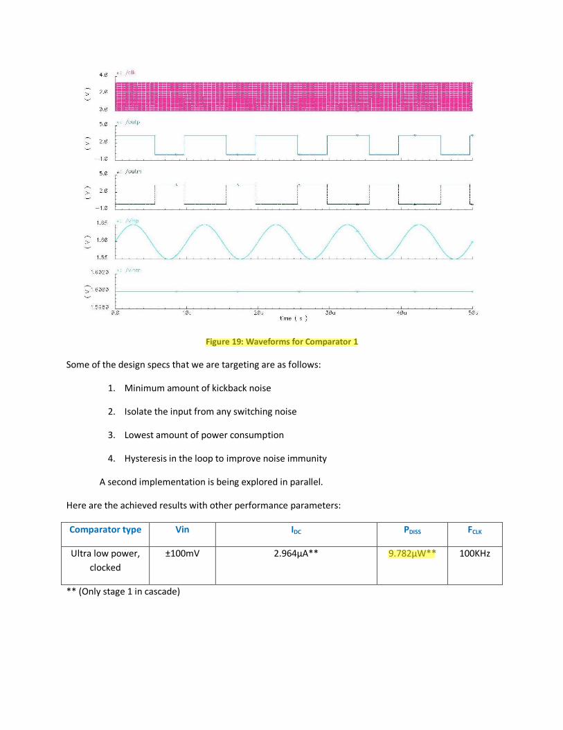
Figure 19: Waveforms for Comparator 1
Some of the design specs that we are targeting are as follows:
1. Minimum amount of kickback noise
2. Isolate the input from any switching noise
3. Lowest amount of power consumption
4. Hysteresis in the loop to improve noise immunity
A second implementation is being explored in parallel.
Here are the achieved results with other performance parameters:
Comparator type Vin IDC PDISS FCLK
Ultra low power,
clocked
±100mV 2.964µA** 9.782µW** 100KHz
** (Only stage 1 in cascade)
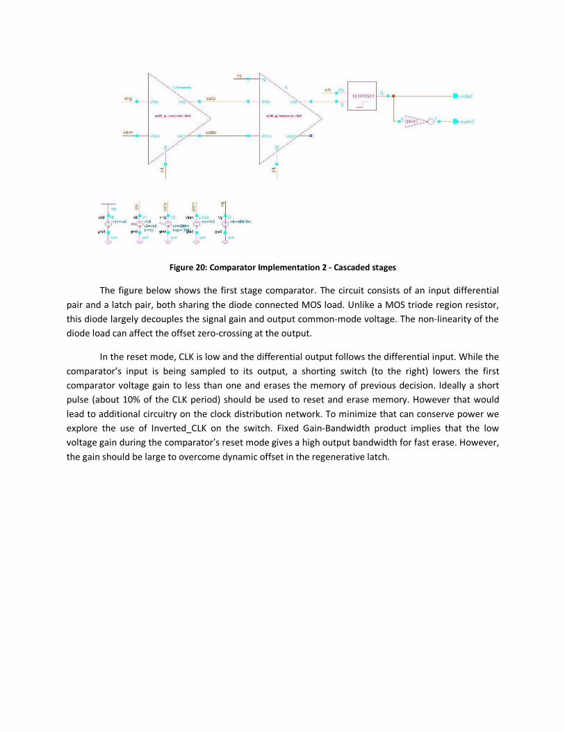
Figure 20: Comparator Implementation 2 - Cascaded stages
The figure below shows the first stage comparator. The circuit consists of an input differential
pair and a latch pair, both sharing the diode connected MOS load. Unlike a MOS triode region resistor,
this diode largely decouples the signal gain and output common-mode voltage. The non-linearity of the
diode load can affect the offset zero-crossing at the output.
In the reset mode, CLK is low and the differential output follows the differential input. While the
comparator’s input is being sampled to its output, a shorting switch (to the right) lowers the first
comparator voltage gain to less than one and erases the memory of previous decision. Ideally a short
pulse (about 10% of the CLK period) should be used to reset and erase memory. However that would
lead to additional circuitry on the clock distribution network. To minimize that can conserve power we
explore the use of Inverted_CLK on the switch. Fixed Gain-Bandwidth product implies that the low
voltage gain during the comparator’s reset mode gives a high output bandwidth for fast erase. However,
the gain should be large to overcome dynamic offset in the regenerative latch.
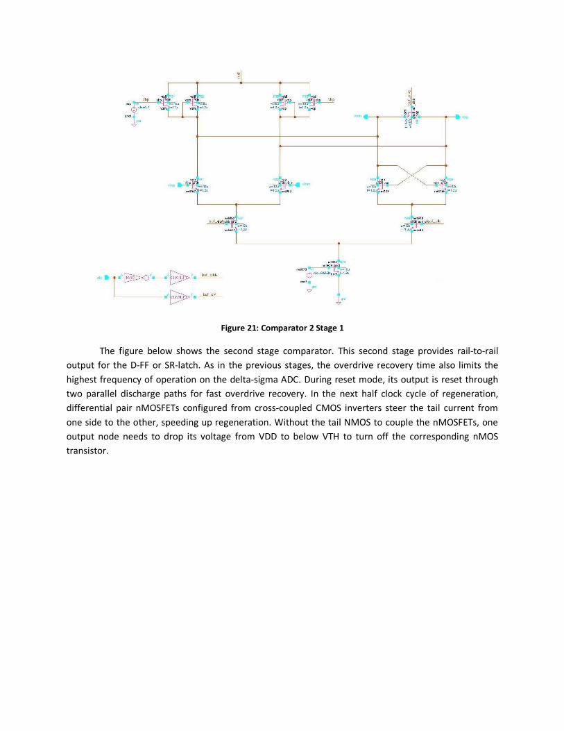
Figure 21: Comparator 2 Stage 1
The figure below shows the second stage comparator. This second stage provides rail-to-rail
output for the D-FF or SR-latch. As in the previous stages, the overdrive recovery time also limits the
highest frequency of operation on the delta-sigma ADC. During reset mode, its output is reset through
two parallel discharge paths for fast overdrive recovery. In the next half clock cycle of regeneration,
differential pair nMOSFETs configured from cross-coupled CMOS inverters steer the tail current from
one side to the other, speeding up regeneration. Without the tail NMOS to couple the nMOSFETs, one
output node needs to drop its voltage from VDD to below VTH to turn off the corresponding nMOS
transistor.
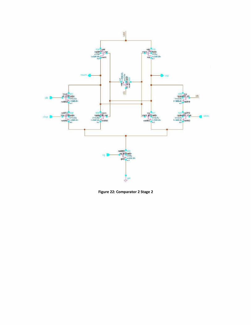
Figure 22: Comparator 2 Stage 2
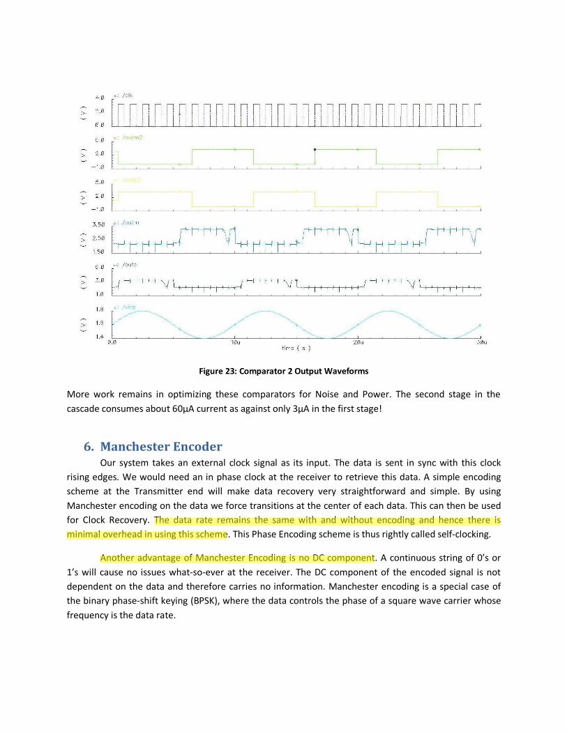
Figure 23: Comparator 2 Output Waveforms
More work remains in optimizing these comparators for Noise and Power. The second stage in the
cascade consumes about 60µA current as against only 3µA in the first stage!
6. Manchester Encoder
Our system takes an external clock signal as its input. The data is sent in sync with this clock
rising edges. We would need an in phase clock at the receiver to retrieve this data. A simple encoding
scheme at the Transmitter end will make data recovery very straightforward and simple. By using
Manchester encoding on the data we force transitions at the center of each data. This can then be used
for Clock Recovery. The data rate remains the same with and without encoding and hence there is
minimal overhead in using this scheme. This Phase Encoding scheme is thus rightly called self-clocking.
Another advantage of Manchester Encoding is no DC component. A continuous string of 0’s or
1’s will cause no issues what-so-ever at the receiver. The DC component of the encoded signal is not
dependent on the data and therefore carries no information. Manchester encoding is a special case of
the binary phase-shift keying (BPSK), where the data controls the phase of a square wave carrier whose
frequency is the data rate.

Figure 24: Manchester Encoding
Here is the implementation of the Manchester Encoder on our design. The second figure shows
the waveforms with a clock of 1MHz. The final data rate will be decided after the optimization of the
Delta-Sigma loop.
Figure 25: Manchester Encoder Schematic
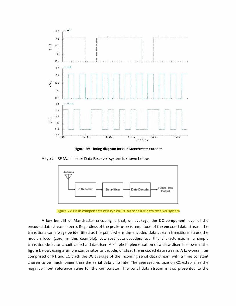
Figure 26: Timing diagram for our Manchester Encoder
A typical RF Manchester Data Receiver system is shown below.
Figure 27: Basic components of a typical RF Manchester data receiver system
A key benefit of Manchester encoding is that, on average, the DC component level of the
encoded data stream is zero. Regardless of the peak-to-peak amplitude of the encoded data stream, the
transitions can always be identified as the point where the encoded data stream transitions across the
median level (zero, in this example). Low-cost data-decoders use this characteristic in a simple
transition-detector circuit called a data-slicer. A simple implementation of a data-slicer is shown in the
figure below, using a simple comparator to decode, or slice, the encoded data stream. A low-pass filter
comprised of R1 and C1 track the DC average of the incoming serial data stream with a time constant
chosen to be much longer than the serial data chip rate. The averaged voltage on C1 establishes the
negative input reference value for the comparator. The serial data stream is also presented to the
positive input of the comparator so that the transitions above and below the average values cause the
comparator output to swing between VDD and zero or between the two supply voltages.
Figure 28: Simple data-slicer circuit for restoring binary logic levels
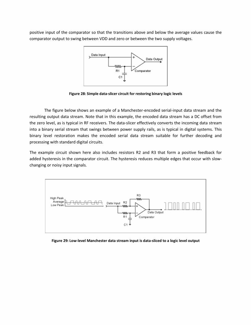
The figure below shows an example of a Manchester-encoded serial-input data stream and the
resulting output data stream. Note that in this example, the encoded data stream has a DC offset from
the zero level, as is typical in RF receivers. The data-slicer effectively converts the incoming data stream
into a binary serial stream that swings between power supply rails, as is typical in digital systems. This
binary level restoration makes the encoded serial data stream suitable for further decoding and
processing with standard digital circuits.
The example circuit shown here also includes resistors R2 and R3 that form a positive feedback for
added hysteresis in the comparator circuit. The hysteresis reduces multiple edges that occur with slow-
changing or noisy input signals.
Figure 29: Low-level Manchester data stream input is data-sliced to a logic level output
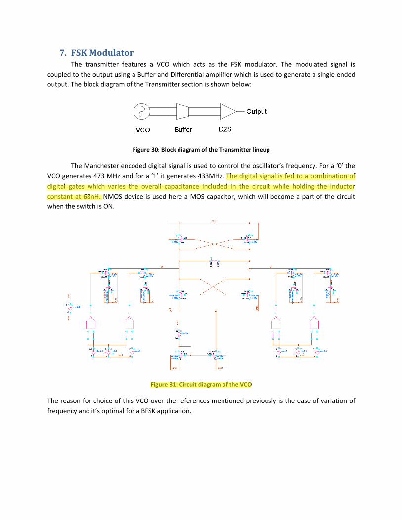
7. FSK Modulator
The transmitter features a VCO which acts as the FSK modulator. The modulated signal is
coupled to the output using a Buffer and Differential amplifier which is used to generate a single ended
output. The block diagram of the Transmitter section is shown below:
Figure 30: Block diagram of the Transmitter lineup
The Manchester encoded digital signal is used to control the oscillator’s frequency. For a ‘0’ the
VCO generates 473 MHz and for a ‘1’ it generates 433MHz. The digital signal is fed to a combination of
digital gates which varies the overall capacitance included in the circuit while holding the inductor
constant at 68nH. NMOS device is used here a MOS capacitor, which will become a part of the circuit
when the switch is ON.
Figure 31: Circuit diagram of the VCO
The reason for choice of this VCO over the references mentioned previously is the ease of variation of
frequency and it’s optimal for a BFSK application.
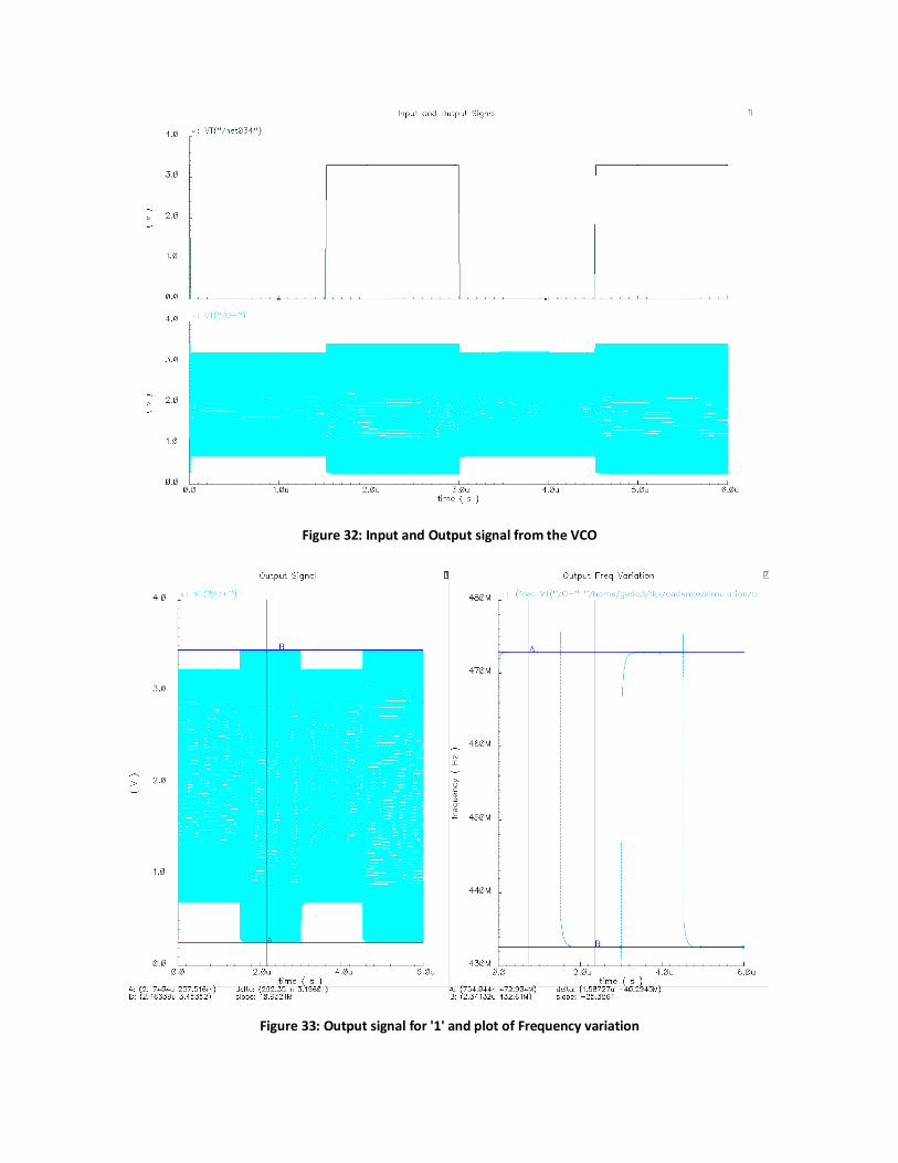
Figure 32: Input and Output signal from the VCO
Figure 33: Output signal for '1' and plot of Frequency variation
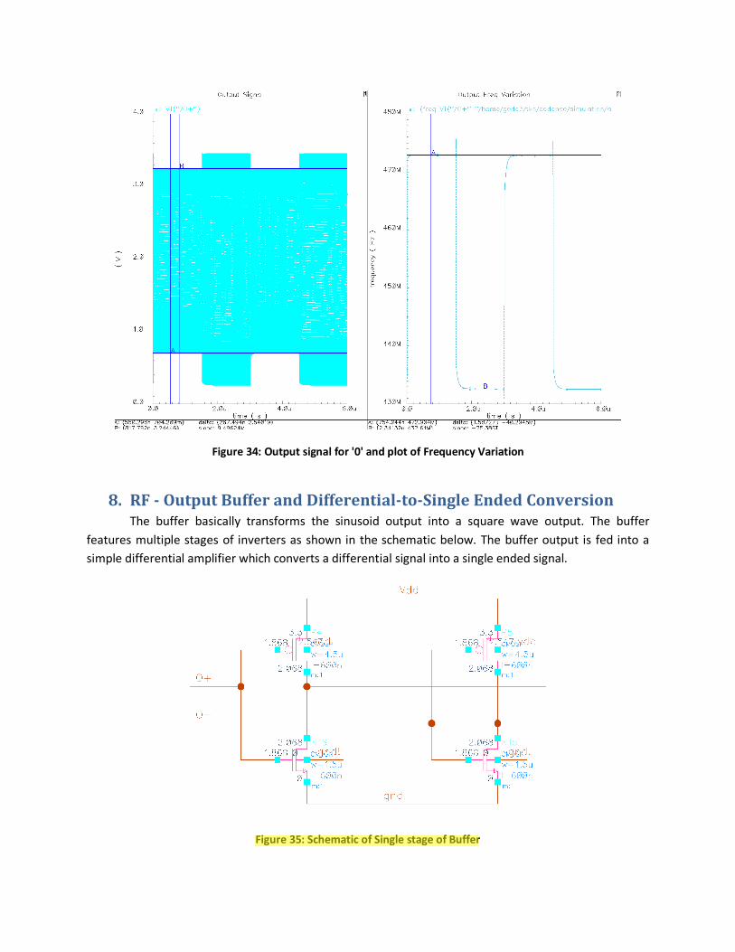
Figure 34: Output signal for '0' and plot of Frequency Variation
8. RF - Output Buffer and Differential-to-Single Ended Conversion
The buffer basically transforms the sinusoid output into a square wave output. The buffer
features multiple stages of inverters as shown in the schematic below. The buffer output is fed into a
simple differential amplifier which converts a differential signal into a single ended signal.
Figure 35: Schematic of Single stage of Buffer
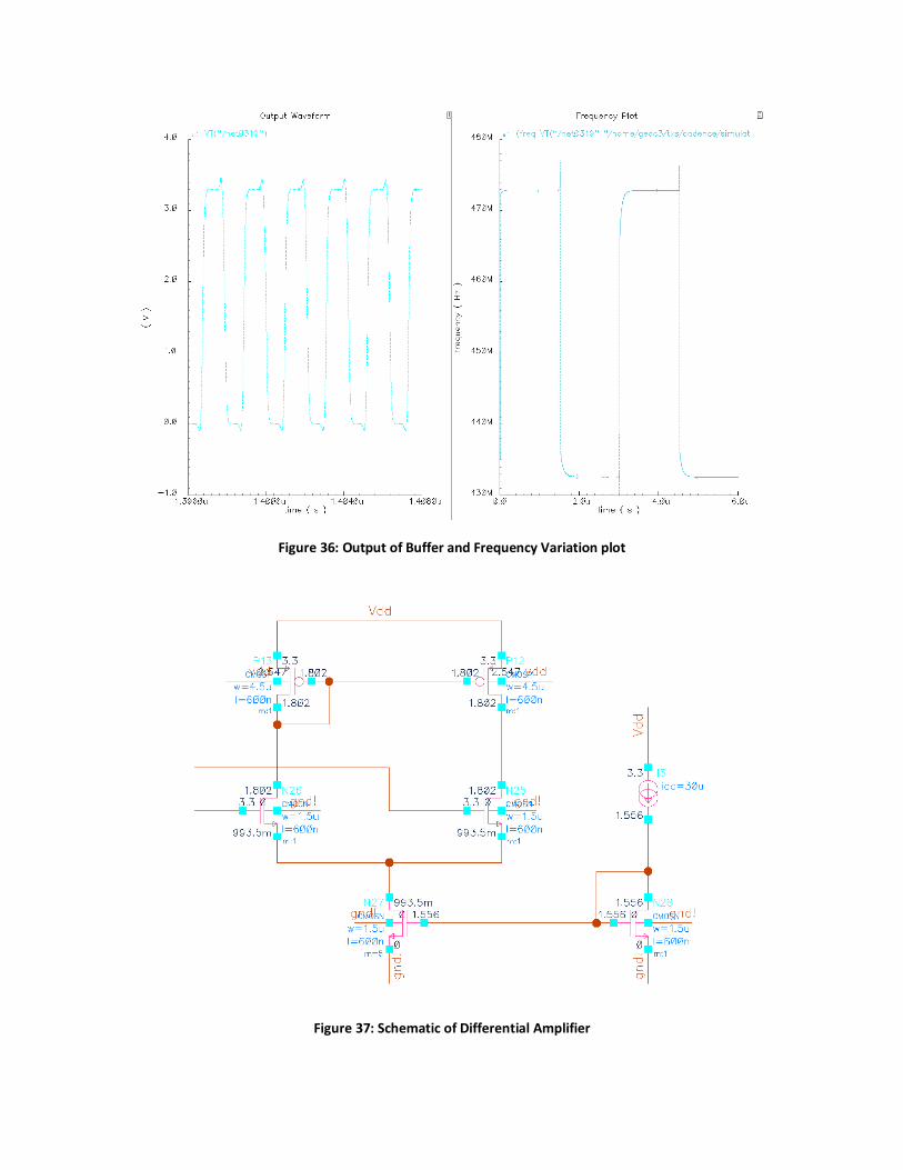
Figure 36: Output of Buffer and Frequency Variation plot
Figure 37: Schematic of Differential Amplifier
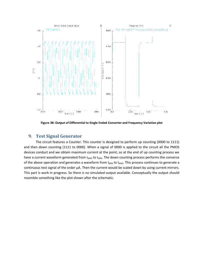
Figure 38: Output of Differential to Single Ended Converter and Frequency Variation plot
9. Test Signal Generator
The circuit features a Counter. This counter is designed to perform up counting (0000 to 1111)
and then down counting (1111 to 0000). When a signal of 0000 is applied to the circuit all the PMOS
devices conduct and we obtain maximum current at the point, so at the end of up counting process we
have a current waveform generated from IMAX to IMIN. The down counting process performs the converse
of the above operation and generates a waveform from IMIN to IMAX. This process continues to generate a
continuous test signal of the order µA. Then the current would be scaled down by using current mirrors.
This part is work in progress. So there is no simulated output available. Conceptually the output should
resemble something like the plot shown after the schematic.
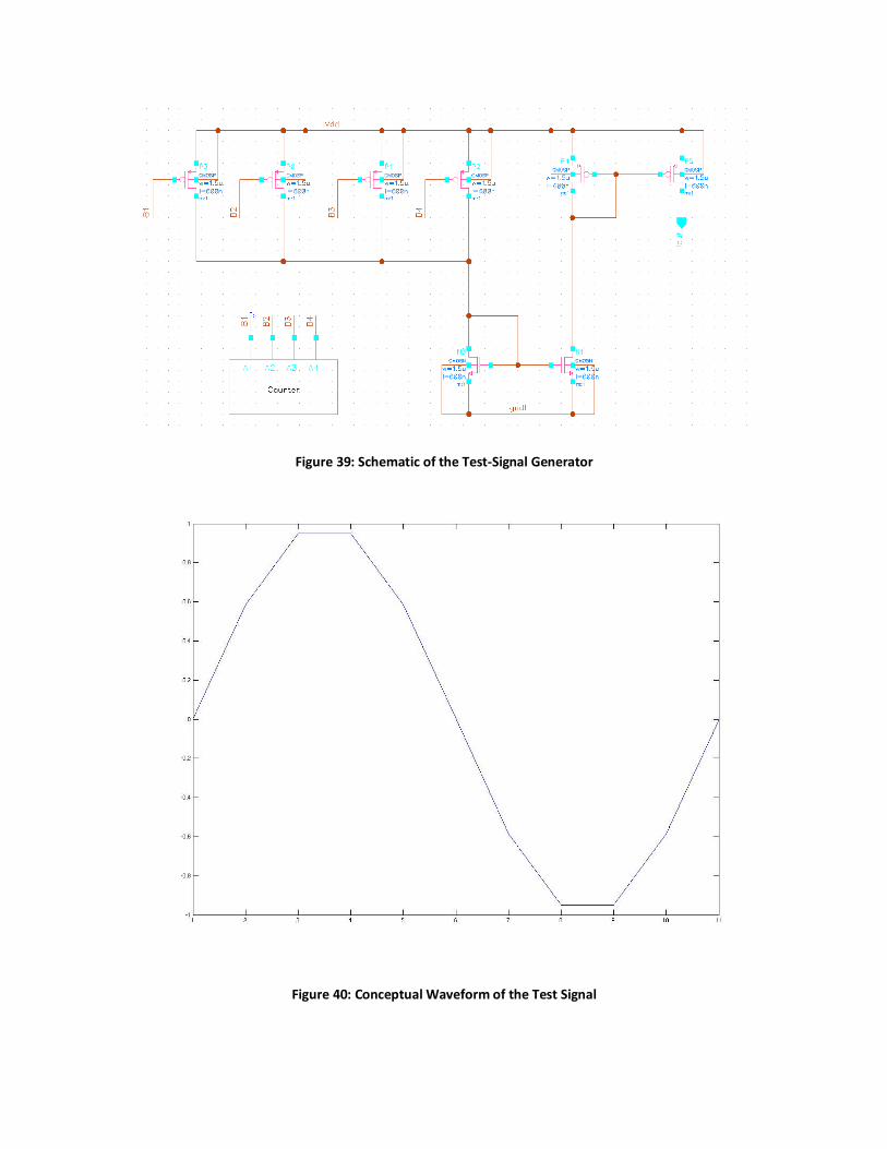
Figure 39: Schematic of the Test-Signal Generator
Figure 40: Conceptual Waveform of the Test Signal
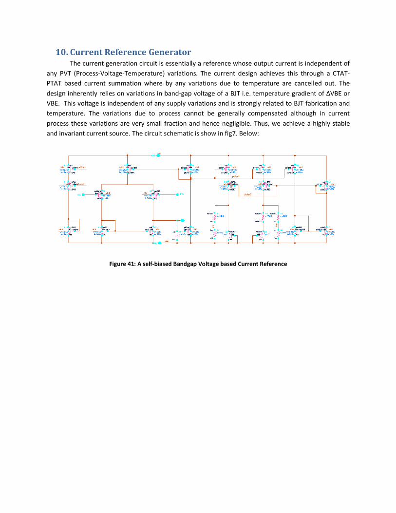
10. Current Reference Generator
The current generation circuit is essentially a reference whose output current is independent of
any PVT (Process-Voltage-Temperature) variations. The current design achieves this through a CTAT-
PTAT based current summation where by any variations due to temperature are cancelled out. The
design inherently relies on variations in band-gap voltage of a BJT i.e. temperature gradient of ∆VBE or
VBE. This voltage is independent of any supply variations and is strongly related to BJT fabrication and
temperature. The variations due to process cannot be generally compensated although in current
process these variations are very small fraction and hence negligible. Thus, we achieve a highly stable
and invariant current source. The circuit schematic is show in fig7. Below:
Figure 41: A self-biased Bandgap Voltage based Current Reference

Figure 42: Temperature characteristic of the Current Reference
The current design achieves a temperature coefficient of the order of 200ppm which is suitable
for current design requirements where we do not expect any significant temperature fluctuations under
test conditions. The loop has been compensated with a 4.8pF capacitor to give 80 degree phase margin
which is essential for a DC bias circuit. The current consumption is presently ~150uA with a reference
current of 24uA. This is a test implementation as we will reduce the reference currents to nearly 500nA
and reduce the power consumption as well.
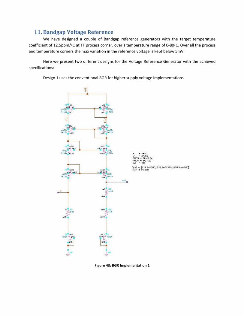
11. Bandgap Voltage Reference
We have designed a couple of Bandgap reference generators with the target temperature
coefficient of 12.5ppm/◦C at TT process corner, over a temperature range of 0-80◦C. Over all the process
and temperature corners the max variation in the reference voltage is kept below 5mV.
Here we present two different designs for the Voltage Reference Generator with the achieved
specifications:
Design 1 uses the conventional BGR for higher supply voltage implementations.
Figure 43: BGR Implementation 1
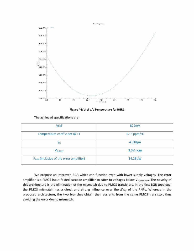
Figure 44: Vref v/s Temperature for BGR1
The achieved specifications are:
Vref 829mV
Temperature coefficient @ TT 17.5 ppm/◦C
IDC 4.318µA
VSUPPLY 3.3V nom
PDISS (inclusive of the error amplifier) 14.25µW
We propose an improved BGR which can function even with lower supply voltages. The error
amplifier is a PMOS input folded cascode amplifier to cater to voltages below VSUPPLY-MID. The novelty of
this architecture is the elimination of the mismatch due to PMOS transistors. In the first BGR topology,
the PMOS mismatch has a direct and strong influence over the ΔVBE of the PNPs. Whereas in the
proposed architecture, the two branches obtain their currents from the same PMOS transistor, thus
avoiding the error due to mismatch.
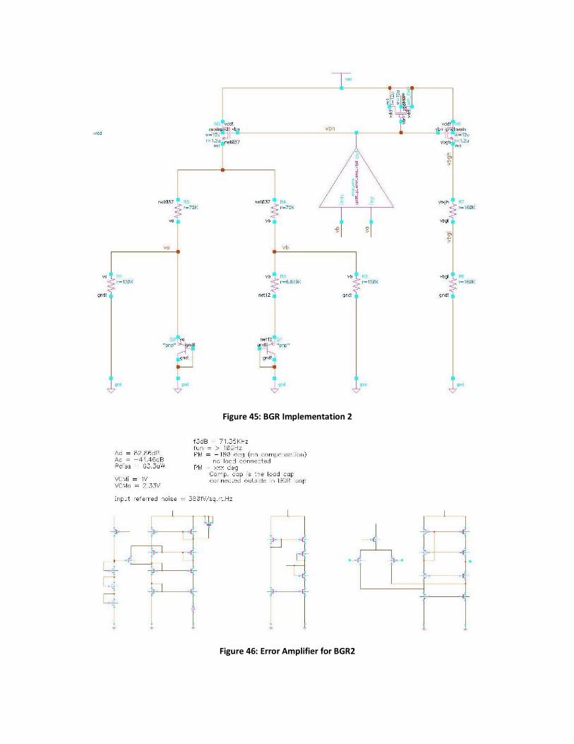
Figure 45: BGR Implementation 2
Figure 46: Error Amplifier for BGR2
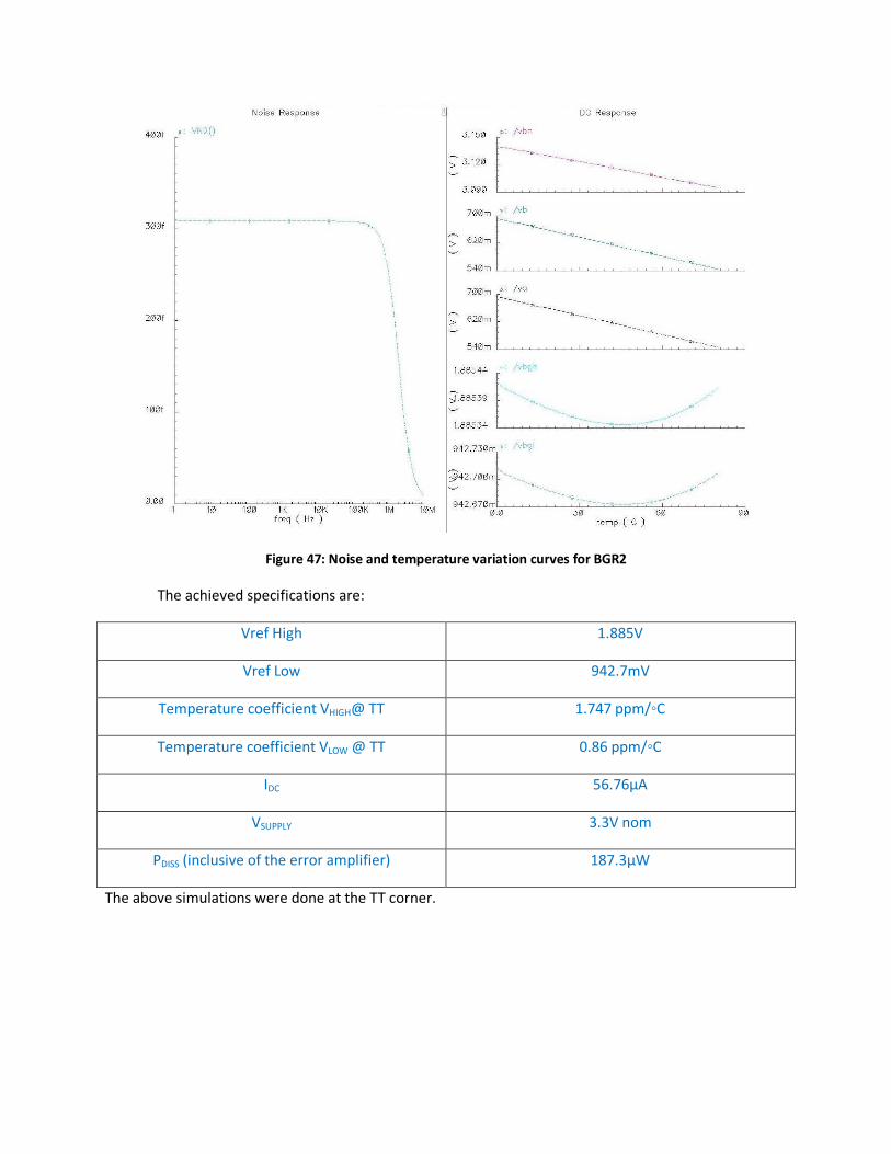
Figure 47: Noise and temperature variation curves for BGR2
The achieved specifications are:
Vref High 1.885V
Vref Low 942.7mV
Temperature coefficient VHIGH@ TT 1.747 ppm/◦C
Temperature coefficient VLOW @ TT 0.86 ppm/◦C
IDC 56.76µA
VSUPPLY 3.3V nom
PDISS (inclusive of the error amplifier) 187.3µW
The above simulations were done at the TT corner.

12. Project Timeline
Here is an update on the timelines for developing this one-chip neural sensor interface solution:
a) Proposed Timeline
Week Task
Feb 2nd
Week Design & Simulation of circuits
Feb 3rd
Week Improve the design by optimizing for low current operation
Mar 1st
Week
Continue optimizing the design, obtain the Input and Output data details from
the blocks before yours and try to alter your circuit so that it fits into the overall
system
Mar 3rd
Week Complete Chain Simulation
Mar 4th
– Apr 1st
Week Floor Planning for the whole chip and kick start the layout process
Apr 2nd
to Tapeout Complete layout , parasitic extraction and simulate circuits to see the effect of
parasitics
b) Proposed Deadlines
Deadline Deliverable
Feb 21st
First cut of the corresponding circuit / system design
Feb 26th
Implement the first cut system in Cadence with the signal chain from Analog
front end through to the RF Transmitter Section
Mar 2nd
Submission of draft 2
Mar 21st
Final version of all circuits design in Cadence verified for PVT and other possible
variations
Mar 29th
Final version of whole chain tested for various input conditions
Apr 4th
Obtain a first cut floor planning for the chip
Apr 12th
Finalize floor planning
Apr 21st
Completion of layout of every circuit in the whole chain
Apr 25th
Post layout simulations to evaluate the effect of parasitic on the performance
Apr 27th
Tapeout
Apr 29th
Final Project Report Submission
c) Progress Report
Circuit / Block Progress in % - Schematics
Current Sensor and top level modeling 70%
Integrator 70%
Comparator 70%

Digital Encoder 100%
FSK Modulator 100%
RF Buffer and D2S converter 70%
BGR Voltage Reference 100%
Current Reference 100%
Testability – Test Signal Generator 30%
Complete Lineup and Simulations 30%
13. References 1. M. Roham, D. P. Daberkow, E. S. Ramsson, D. P. Covey, S. Pakdeeronachit, P. A. Garris and P. Mohseni, “A
Wireless IC for Wide-Range Neurochemical Monitoring Using Amperometry and Fast-Scan Cyclic
Voltammetry,” IEEE Transactions on Biomedical Circuits and Systems, vol. 2, no. 1, March 2008
2. J. . Janata, “Electrochemical Microsensors,” IEEE Proceedings, vol. 91, Issue 6, pp. 864-869, June 2003
3. L. Zhang, Z. Yu and X. He, “Circuit Design and Verification of On-Chip Femto-Ampere Current Mode Circuit
Using 0.18um CMOS Technology,” Solid State and Integrated Circuit Technology, 2006
4. Y. W Choi & Howard C Luong, “High Q & Wide Dynamic range CMOS BPF for Wireless Rx“, IEEE
Transaction on Circuits & Systems, May 2001.
5. Behzad Razavi, “RF Transmitter Architectures”, IEEE Proceedings of Custom Integrated Circuits, 1999.
6. M. Stanacevic, K. Murari, A. Rege, G. Cauwenberghs and N. Thakor, “VLSI Potentiostat Array with
Oversampling Gain Modulation for Wide-Range Neurotransmitter Sensing,” IEEE Transactions on
Biochemical Circuits and Systems, vol. 1, no.1, March 2007
7. R. J. Baker, “CMOS Circuit Design, Layout, and Simulation”, Wiley-interscience. Second Edition.
8. Lamb, K.G.; Sanchez, S.J.; Holman, W.T, "A low noise operational amplifier design using subthreshold
operation", IEEE Proceedings of the 40th Midwest Symposium on Circuits and Systems, 1997. Volume 1,
3-6 Aug. 1997 Page(s):35 - 38.
9. Zhiyuan Li; Jianguo Ma; Mingyan Yu; Yizheng Ye, "Low noise operational amplifier design with current
driving bulk in 0.25μm CMOS technology", IEEE Proceedings of the 6th International Conference On ASIC,
2005. ASICON 2005. Volume 2, 24-27 Oct. 2005 Page(s):630 - 634