Embed Size (px)
Citation preview

1

AN FPGA BASED BLDC MOTOR CONTROL SYSTEM
A THESIS SUBMITTED TOTHE GRADUATE SCHOOL OF NATURAL AND APPLIED SCIENCES
OFMIDDLE EAST TECHNICAL UNIVERSITY
BY
SERDAR UYGUR
IN PARTIAL FULFILLMENT OF THE REQUIREMENTSFOR
THE DEGREE OF MASTER OF SCIENCEIN
ELECTRICAL AND ELECTRONICS ENGINEERING
FEBRUARY 2012
Approval of the thesis:
AN FPGA BASED BLDC MOTOR CONTROL SYSTEM
submitted by SERDAR UYGUR in partial fulfillment of the requirements for the degree ofMaster of Science in Electrical and Electronics Engineering Department, Middle EastTechnical University by,
Prof. Dr. Canan OZGENDean, Graduate School of Natural and Applied Sciences
Prof. Dr. Ismet ERKMENHead of Department, Electrical and Electronics Engineering
Prof. Dr. Hasan Cengiz GuranSupervisor, Electrical and Electronics Engineering Dept., METU
Examining Committee Members:
Prof. Dr. Muammer ERMISElectrical and Electronics Engineering Dept., METU
Prof. Dr. Hasan Cengiz GURANElectrical and Electronics Engineering Dept., METU
Assoc. Prof. Dr. Cuneyt F. BAZLAMACCIElectrical and Electronics Engineering Dept., METU
Assist. Prof. Dr. Ilkay ULUSOYElectrical and Electronics Engineering Dept., METU
Ali YILMAZKOCLAR, M.Sc.TUBITAK-SAGE, ETB
Date:

I hereby declare that all information in this document has been obtained and presentedin accordance with academic rules and ethical conduct. I also declare that, as requiredby these rules and conduct, I have fully cited and referenced all material and results thatare not original to this work.
Name, Last Name: SERDAR UYGUR
Signature :
iii

ABSTRACT
AN FPGA BASED BLDC MOTOR CONTROL SYSTEM
Uygur, Serdar
M.Sc., Department of Electrical and Electronics Engineering
Supervisor : Prof. Dr. Hasan Cengiz Guran
February 2012, 148 pages
In this thesis, position and current control systems for a brushless DC (Direct Current) motor
are designed and integrated into one FPGA (Field Programmable Gate Array) chip. Experi-
mental results are obtained by driving the brushless DC motors of Control Actuation System
of a guided missile. Because of their high performance, brushless DC motors are widely used
in Control Actuation Systems of guided missiles. In order to control the motor torque, cur-
rent controller is designed and implemented in the FPGA. Position controller is designed to
fulfill the position commands. A soft processor in the FPGA is used to connect and configure
the current controller, position sensor interfaces and communication modules such as UART
(Universal Asynchronous Receiver Transmitter) and Spacewire. In addition; position con-
troller is implemented in the soft processor in the FPGA. An FPGA based electronic board is
designed and manufactured to implement control algorithms, power converter circuitry and to
perform other tasks such as communication with PC (Personal Computer). In order to mon-
itor the behavior of the controllers in real time and to achieve performance tests, a graphical
user interface is provided.
Keywords: Brushless DC Motor, Current Control, Position Control, FPGA, Soft Processor
iv
OZ
FPGA TABANLI FIRCASIZ DOGRU AKIM MOTOR KONTROL SISTEMI
Uygur, Serdar
Yuksek Lisans, Elektrik Elektronik Muhendisligi Bolumu
Tez Yoneticisi : Prof. Dr. Hasan Cengiz GURAN
Subat 2012, 148 sayfa
Bu tezde fırcasız dogru akım motoru icin pozisyon ve akım kontrol sistemleri tasarlanmıs ve
alan programlanabilir kapılar dizisinde (FPGA) calıstırılmıstır. Deneysel sonuclar gudumlu
bir fuzenin kanat tahrik sistemindeki fırcasız dogru akım motorları kontrol edilerek elde
edilmistir. Fırcasız dogru akım motorları yuksek performanslarından dolayı gudumlu fuzelerin
kanat tahrik sistemlerinde yaygın olarak kullanılmaktadır. Motor torkunu kontrol etmek icin
akım kontrolcu tasarlanmıs ve alan programlanabilir kapılar dizisinde (FPGA) calıstırılmıstır.
Sonra pozisyon komutlarını yerine getirmek icin pozsiyon kontrolcu tasarlanmıstır. Akım
kontrolcu, pozisyon algılayıcı arayuzu ve haberlesme modullerini (UART, Spacewire) bir-
birine baglamak ve modulleri konfigure etmek icin alan programlanabilir kapılar dizisinde
yazılımsal islemci kullanılmıstır. Buna ek olarak pozisyon kontrolcu yazılımsal islemci uzerinde
calıstırılmıstır. Kontrol algoritmalarını, guc cevirici devresini calıstırmak ve kullanıcı bil-
gisayarı ile haberlesmek icin alan programlanabilir kapılar dizisi tabanlı bir elektronik kart
tasarlanmıs ve uretilmistir. Kontrol algoritmalarının davranıslarını gercek zamanlı izlemek
icin ve performans testlerini gerceklestirebilmek icin bir kullanıcı arayuz programı hazırlanmıstır.
v

Anahtar Kelimeler: Fırcasız Dogru Akım Motoru, Akım Kontrol, Pozisyon Kontrol, FPGA,
Yazılımsal Islemci
vi

To My Family,To My Fiance
vii

ACKNOWLEDGMENTS
I would like to thank my supervisor Prof. Dr. Hasan Cengiz GURAN, for his guidance, under-
standing and patience. Throughout the preparation of this thesis, he provided encouragement,
sound advice, and lots of good ideas.
I am very grateful to TUBITAK-SAGE for providing tools and other facilities throughout the
production of my thesis.
I would like to show my gratitude to colleagues, who supported this work in both technical
and moral aspects.
I would like to thank my family and fiance for all their help during my thesis.
viii

TABLE OF CONTENTS
ABSTRACT . . . . . . . . . . . . . . . . . . . . . . . . . . . . . . . . . . . . . . . . iv
OZ . . . . . . . . . . . . . . . . . . . . . . . . . . . . . . . . . . . . . . . . . . . . . v
ACKNOWLEDGMENTS . . . . . . . . . . . . . . . . . . . . . . . . . . . . . . . . . viii
TABLE OF CONTENTS . . . . . . . . . . . . . . . . . . . . . . . . . . . . . . . . . ix
LIST OF TABLES . . . . . . . . . . . . . . . . . . . . . . . . . . . . . . . . . . . . xi
LIST OF FIGURES . . . . . . . . . . . . . . . . . . . . . . . . . . . . . . . . . . . . xiii
LIST OF ABBREVIATIONS . . . . . . . . . . . . . . . . . . . . . . . . . . . . . . . xx
CHAPTERS
1 INTRODUCTION AND MOTIVATION . . . . . . . . . . . . . . . . . . . . 1
2 MOTOR DRIVER CONTROL SYSTEM DESIGN . . . . . . . . . . . . . . 6
2.1 Electronic Board Design . . . . . . . . . . . . . . . . . . . . . . . . 6
2.1.1 Structure of the FPGA Design . . . . . . . . . . . . . . . 17
2.2 Graphical User Interface Design . . . . . . . . . . . . . . . . . . . 23
2.3 Test Setup . . . . . . . . . . . . . . . . . . . . . . . . . . . . . . . 26
3 DESIGN AND IMPLEMENTATION OF CURRENT CONTROLLER . . . . 30
3.1 Current Controller Design . . . . . . . . . . . . . . . . . . . . . . . 31
3.1.1 Current Acquisition . . . . . . . . . . . . . . . . . . . . . 39
3.1.2 Phase Detection . . . . . . . . . . . . . . . . . . . . . . . 47
ix

3.1.3 Current Integrator . . . . . . . . . . . . . . . . . . . . . . 50
3.1.4 Average Current Calculation . . . . . . . . . . . . . . . . 55
3.1.5 Offset Current Detection . . . . . . . . . . . . . . . . . . 59
3.1.6 Offset Current Subtraction . . . . . . . . . . . . . . . . . 65
3.1.7 Error Current Calculation . . . . . . . . . . . . . . . . . . 69
3.1.8 PI Controller . . . . . . . . . . . . . . . . . . . . . . . . 75
3.1.9 Pulse Width Generator . . . . . . . . . . . . . . . . . . . 82
3.1.10 Commutation Control . . . . . . . . . . . . . . . . . . . . 87
3.2 Bus Controller Design . . . . . . . . . . . . . . . . . . . . . . . . . 92
3.3 Matlab Simulations . . . . . . . . . . . . . . . . . . . . . . . . . . 104
3.4 Experimental Results . . . . . . . . . . . . . . . . . . . . . . . . . 112
4 POSITION CONTROLLER DESIGN AND IMPLEMENTATION . . . . . . 121
4.1 PID Controller . . . . . . . . . . . . . . . . . . . . . . . . . . . . . 124
4.2 I-PD Controller . . . . . . . . . . . . . . . . . . . . . . . . . . . . 127
4.3 Encoder Interface . . . . . . . . . . . . . . . . . . . . . . . . . . . 130
4.4 Matlab Simulations . . . . . . . . . . . . . . . . . . . . . . . . . . 131
4.5 Experimental Results . . . . . . . . . . . . . . . . . . . . . . . . . 138
5 CONCLUSION . . . . . . . . . . . . . . . . . . . . . . . . . . . . . . . . . 144
REFERENCES . . . . . . . . . . . . . . . . . . . . . . . . . . . . . . . . . . . . . . 147
x

LIST OF TABLES
TABLES
Table 2.1 Summary of the FPGA utilization characteristics for the motor control system 19
Table 3.1 Configurable Parameters of the Current Controller Module . . . . . . . . . 34
Table 3.2 Input, Output ports of the Current Controller Module . . . . . . . . . . . . 36
Table 3.3 Continuation of the Input, Output ports of the Current Controller Module . 37
Table 3.4 Input, Output ports of the Current Acquisition Module . . . . . . . . . . . 41
Table 3.5 Current sensor and ADC sensitivity parameters . . . . . . . . . . . . . . . 44
Table 3.6 Inputs and Outputs of the Phase Current Detection State Machine . . . . . . 47
Table 3.7 Port Decsriptions of the Phase Detection Module . . . . . . . . . . . . . . 49
Table 3.8 Port Decsriptions of the Current Integrator Module . . . . . . . . . . . . . 51
Table 3.9 Port Decsriptions of the Average Current Calculation Module . . . . . . . . 57
Table 3.10 Port Decsriptions of the Offset Detection Module . . . . . . . . . . . . . . 62
Table 3.11 Motor Excitation and Sensor Outputs for Clockwise Rotation . . . . . . . . 87
Table 3.12 Commutation Table of the Motor . . . . . . . . . . . . . . . . . . . . . . . 87
Table 3.13 Port Decsriptions of the Bus Controller VHDL Module . . . . . . . . . . . 93
Table 3.14 Registers of the Bus Controller Module . . . . . . . . . . . . . . . . . . . . 94
Table 3.15 Spacewire Packet Structure . . . . . . . . . . . . . . . . . . . . . . . . . . 102
xi

Table 4.1 PID System Parameters for ξ = 1 . . . . . . . . . . . . . . . . . . . . . . . 126
Table 4.2 I-PD System Parameters for ξ = 1 . . . . . . . . . . . . . . . . . . . . . . 129
xii

LIST OF FIGURES
FIGURES
Figure 1.1 Block Diagram of the Control System . . . . . . . . . . . . . . . . . . . . 4
Figure 2.1 General Diagram of the Motor Control System . . . . . . . . . . . . . . . 7
Figure 2.2 Block Diagram of the Electronic Board . . . . . . . . . . . . . . . . . . . 8
Figure 2.3 Data-Strobe Encoding . . . . . . . . . . . . . . . . . . . . . . . . . . . . 11
Figure 2.4 Structure of the Inverter Circuit . . . . . . . . . . . . . . . . . . . . . . . 12
Figure 2.5 Functional Block Diagram of Isolation Chip [14] . . . . . . . . . . . . . . 12
Figure 2.6 Functional Block Diagram of Motor Driver Circuit . . . . . . . . . . . . . 13
Figure 2.7 Current measurement with three shunt resistors . . . . . . . . . . . . . . . 14
Figure 2.8 Functional Block Diagram of the Current Sensor [16] . . . . . . . . . . . 15
Figure 2.9 Functional Block Diagram of the Current Sensing Circuit . . . . . . . . . 16
Figure 2.10 Functional Block Diagram of the FPGA Design . . . . . . . . . . . . . . . 18
Figure 2.11 Functional Block Diagram of the Microblaze Processor Core [17] . . . . . 20
Figure 2.12 Three Stage Pipeline Structure of the Microblaze Core [17] . . . . . . . . 21
Figure 2.13 Settings Part of the GUI . . . . . . . . . . . . . . . . . . . . . . . . . . . 23
Figure 2.14 Current Control Test Parameters Window of the GUI . . . . . . . . . . . . 24
Figure 2.15 Position Control Test Parameters Window of the GUI . . . . . . . . . . . . 25
xiii

Figure 2.16 Test Control Part of the GUI . . . . . . . . . . . . . . . . . . . . . . . . . 26
Figure 2.17 Test Results of a Current Control Experiment . . . . . . . . . . . . . . . . 27
Figure 2.18 Structure of the Test Setup . . . . . . . . . . . . . . . . . . . . . . . . . . 28
Figure 2.19 An Overview of the SpaceWire Brick Hardware Architecture [18] . . . . . 29
Figure 3.1 Functional Block Diagram of the Current Controller . . . . . . . . . . . . 32
Figure 3.2 Structure of the Current Controller VHDL Module . . . . . . . . . . . . . 33
Figure 3.3 Configurable parameters window of the current controller on the EDK plat-
form . . . . . . . . . . . . . . . . . . . . . . . . . . . . . . . . . . . . . . . . . 35
Figure 3.4 Flowchart of the current controller VHDL module . . . . . . . . . . . . . 38
Figure 3.5 Structure of the current acquisition block . . . . . . . . . . . . . . . . . . 40
Figure 3.6 Serial Interface Timing Diagram of AD7944 chip [19] . . . . . . . . . . . 43
Figure 3.7 Simulation of ADC Driver Code for One Sampling Cycle . . . . . . . . . 43
Figure 3.8 Current Scaling of the Negative-Valued Currents . . . . . . . . . . . . . . 45
Figure 3.9 Flowchart of the current acquisition block . . . . . . . . . . . . . . . . . . 46
Figure 3.10 State Machine Diagram of the Phase Detection VHDL Module . . . . . . 48
Figure 3.11 Phase detection VHDL module . . . . . . . . . . . . . . . . . . . . . . . 49
Figure 3.12 Sampling of the Current Feedback . . . . . . . . . . . . . . . . . . . . . . 50
Figure 3.13 Current Integrator VHDL Module . . . . . . . . . . . . . . . . . . . . . . 51
Figure 3.14 Connection between the current integrator module, current acquisition block
and phase detection modules . . . . . . . . . . . . . . . . . . . . . . . . . . . . 53
Figure 3.15 Flowchart of the current integrator block . . . . . . . . . . . . . . . . . . 54
Figure 3.16 Simulation of the Current Integrator . . . . . . . . . . . . . . . . . . . . . 55
xiv

Figure 3.17 Average current calculation . . . . . . . . . . . . . . . . . . . . . . . . . 56
Figure 3.18 Average Current Calculation VHDL Module . . . . . . . . . . . . . . . . 56
Figure 3.19 Simulation of the Average Current Calculation Module . . . . . . . . . . . 57
Figure 3.20 Connection of the average current calculation module with the other modules 58
Figure 3.21 Flowchart of the offset current detection VHDL module . . . . . . . . . . 60
Figure 3.22 Offset Detection VHDL Module . . . . . . . . . . . . . . . . . . . . . . . 61
Figure 3.23 Connection of the offset detection block with the other modules . . . . . . 63
Figure 3.24 Simulation of the Offset Detection Module . . . . . . . . . . . . . . . . . 64
Figure 3.25 Offset current subtraction VHDL module . . . . . . . . . . . . . . . . . . 65
Figure 3.26 Flowchart of the offset current subtraction VHDL module . . . . . . . . . 66
Figure 3.27 Feedback Current Reading Block . . . . . . . . . . . . . . . . . . . . . . 67
Figure 3.28 Top Level View of the Feedback Current Reading Block . . . . . . . . . . 68
Figure 3.29 Simulation Result Window of the Offset Current Subtraction Module . . . 69
Figure 3.30 Error Current Calculation VHDL Module . . . . . . . . . . . . . . . . . . 70
Figure 3.31 Flowchart of the error current calculation VHDL module . . . . . . . . . . 71
Figure 3.32 Connection diagram between the error current calculation module and the
feedback current reading module . . . . . . . . . . . . . . . . . . . . . . . . . . 72
Figure 3.33 Simulation Result Window of the Error Current Calculation Module . . . . 74
Figure 3.34 PI controller VHDL module . . . . . . . . . . . . . . . . . . . . . . . . . 77
Figure 3.35 PI controller state machine . . . . . . . . . . . . . . . . . . . . . . . . . . 78
Figure 3.36 Simulation Result Window of the PI Controller Module . . . . . . . . . . 80
Figure 3.37 Connection of the PI controller module with the other modules . . . . . . . 81
xv
Figure 3.38 PI versus Pulse Width . . . . . . . . . . . . . . . . . . . . . . . . . . . . 82
Figure 3.39 Pulse width generator module . . . . . . . . . . . . . . . . . . . . . . . . 83
Figure 3.40 Flowchart of the pulse width generator VHDL module . . . . . . . . . . . 84
Figure 3.41 Simulation Result Window of the Pulse Width Generator Module . . . . . 85
Figure 3.42 Connection between the pulse width generator module and the other VHDL
modules . . . . . . . . . . . . . . . . . . . . . . . . . . . . . . . . . . . . . . . 86
Figure 3.43 Notation of the Commutation Control’s Outputs on the Inverter Circuit . . 88
Figure 3.44 Commutation Control VHDL Module . . . . . . . . . . . . . . . . . . . . 89
Figure 3.45 Simulation Result Window of the Commutation Control VHDL Module . . 89
Figure 3.46 Current Controller VHDL Module Structure . . . . . . . . . . . . . . . . 90
Figure 3.47 Top Level View of the Current Controller VHDL Module . . . . . . . . . 91
Figure 3.48 Ports of the Bus Controller VHDL Module . . . . . . . . . . . . . . . . . 92
Figure 3.49 Timing diagram of the 20 kHz clock enable signals . . . . . . . . . . . . . 94
Figure 3.50 Control Register of the Current Controller Module . . . . . . . . . . . . . 95
Figure 3.51 Implementation of the Control Register . . . . . . . . . . . . . . . . . . . 96
Figure 3.52 Mapping of the control register to the current controller modules’ ports . . 97
Figure 3.53 Status Register of the Current Controller Module . . . . . . . . . . . . . . 98
Figure 3.54 Mapping between the status register and current control modules . . . . . 99
Figure 3.55 Current Command Register of the Current Controller Module . . . . . . . 100
Figure 3.56 PI Controller Parameters Register of the Current Controller Module . . . . 100
Figure 3.57 Structure of the Feedback Data Control Block . . . . . . . . . . . . . . . . 103
Figure 3.58 MATLAB Model of the Current Controller . . . . . . . . . . . . . . . . . 105
xvi
Figure 3.59 Motor Speed for the 4 A Current Command . . . . . . . . . . . . . . . . . 107
Figure 3.60 Motor Torque for the 4 A Current Command . . . . . . . . . . . . . . . . 107
Figure 3.61 Rectified Current Command and Feedback . . . . . . . . . . . . . . . . . 108
Figure 3.62 Motor Torque for 4A Peak-to-Peak Square Waveform Current Command . 109
Figure 3.63 Current Command and Current Feedback Signals for a 700 Hz Sine Current
Command of 50 A Magnitude . . . . . . . . . . . . . . . . . . . . . . . . . . . . 110
Figure 3.64 Motor Torque for 700 Sine Current Command of 50 A Magnitude . . . . . 110
Figure 3.65 Current Command and Current Feedback Signals for 500 Hz Square Wave
Current Command of 16 A Magnitude . . . . . . . . . . . . . . . . . . . . . . . 111
Figure 3.66 Current Command and Current Feedback Signals for 500 Hz Square Wave
Current Command of 20 A Magnitude . . . . . . . . . . . . . . . . . . . . . . . 111
Figure 3.67 Current Command and Current Feedback Signals for a 50 Hz Square Cur-
rent Command of 4A Magnitude . . . . . . . . . . . . . . . . . . . . . . . . . . 112
Figure 3.68 Oscilloscope View of Current Feedback Signal for a 50 Hz Square Current
Command of 4A Magnitude . . . . . . . . . . . . . . . . . . . . . . . . . . . . . 113
Figure 3.69 Screen Shot of the 25 Hz Sine Current Command of 4A Magnitude . . . . 114
Figure 3.70 Current Command and Current feedback Signals for a 25 Hz Sine Current
Command of 4A Magnitude . . . . . . . . . . . . . . . . . . . . . . . . . . . . . 114
Figure 3.71 Oscilloscope View of Current feedback Signal for a 25 Hz Sine Current
Command of 4A Magnitude . . . . . . . . . . . . . . . . . . . . . . . . . . . . . 115
Figure 3.72 Current Command and Current feedback Signals for a 100 Hz Square Cur-
rent Command of 4A Magnitude . . . . . . . . . . . . . . . . . . . . . . . . . . 116
Figure 3.73 Overshoot of Current Feedback Signal for a 100 Hz Square Current Com-
mand of 4A Magnitude . . . . . . . . . . . . . . . . . . . . . . . . . . . . . . . 116
xvii

Figure 3.74 Current Feedback Signal for a 500 Hz Square Current Command of 16A
Magnitude (Experimental result) . . . . . . . . . . . . . . . . . . . . . . . . . . 117
Figure 3.75 Current Feedback Signal for a 500 Hz Square Current Command of 20A
Magnitude (Experimental result) . . . . . . . . . . . . . . . . . . . . . . . . . . 118
Figure 3.76 Maximum Current Magnitude versus Frequency of the Square Wave Cur-
rent Command . . . . . . . . . . . . . . . . . . . . . . . . . . . . . . . . . . . . 119
Figure 3.77 High Current Signal for 1 A Current Limit . . . . . . . . . . . . . . . . . 120
Figure 4.1 Position Control System . . . . . . . . . . . . . . . . . . . . . . . . . . . 121
Figure 4.2 Position control system without the current control loop . . . . . . . . . . 122
Figure 4.3 Position control system without the postion transducer . . . . . . . . . . . 122
Figure 4.4 Position control system with the motor model . . . . . . . . . . . . . . . . 123
Figure 4.5 PID Controlled Position Control System . . . . . . . . . . . . . . . . . . 124
Figure 4.6 Frequency response of the PID controlled position control system . . . . . 125
Figure 4.7 IPD Controlled Position Control System . . . . . . . . . . . . . . . . . . 127
Figure 4.8 Frequency response of the I-PD controlled position control system . . . . . 128
Figure 4.9 State Machine Diagram of the Encoder Interface Module . . . . . . . . . . 130
Figure 4.10 Matlab Model of the I-PD Position Control System . . . . . . . . . . . . . 132
Figure 4.11 Step response of the PID controlled system for 300 degree command . . . 133
Figure 4.12 Current command of the PID controlled system for 300 degree step command134
Figure 4.13 Step response of the I-PD controlled system for 300 degree step command 135
Figure 4.14 Current command of the I-PD controlled system for 300 degree step command135
Figure 4.15 Motor position for PID controlled system and 5 Hz, 300 degree peak to
peak sine command . . . . . . . . . . . . . . . . . . . . . . . . . . . . . . . . . 136
xviii

Figure 4.16 Motor position for I-PD controlled system and 5 Hz, 300 degree peak to
peak sine command . . . . . . . . . . . . . . . . . . . . . . . . . . . . . . . . . 137
Figure 4.17 Motor position for 20 Hz sine position command of 160 degree magnitude 138
Figure 4.18 Step response of the PID controlled system for 300 degree command (ex-
perimental result) . . . . . . . . . . . . . . . . . . . . . . . . . . . . . . . . . . 139
Figure 4.19 Step response of the I-PD controlled system for 300 degree command (ex-
perimental result) . . . . . . . . . . . . . . . . . . . . . . . . . . . . . . . . . . 140
Figure 4.20 Motor position for PID controlled system and 5 Hz, 300 degree peak to
peak sine command (experimental result) . . . . . . . . . . . . . . . . . . . . . . 141
Figure 4.21 Motor position for I-PD controlled system and 5 Hz, 300 degree peak to
peak sine command (experimental result) . . . . . . . . . . . . . . . . . . . . . . 141
Figure 4.22 Motor position for 20 Hz sine position command of 160 degree magnitude
(experimental result) . . . . . . . . . . . . . . . . . . . . . . . . . . . . . . . . . 142
Figure 4.23 Magnitude of the position command versus frequency of the sine wave
position command . . . . . . . . . . . . . . . . . . . . . . . . . . . . . . . . . . 143
xix

LIST OF ABBREVIATIONS
ADC Analog to Digital Converter.
ALU Arithmetic Logic Unit.
ASIC Application Specific Integrated Circuit.
BLDC Brushless Direct Current.
BRAM Block Random Access Memory.
CPU Central Processing Unit.
DC Direct Current.
DCM Digital Clock Manager.
DSP Digital Signal Processor.
EEPROM Electronically Erasable Programmable Read-Only Memory.
EMI Electromagnetic Interference.
FIFO First In First Out.
FPGA Field Programmable Gate Array.
I/O Input Output.
xx
JTAG Joint Test Action Group.
MSPS Mega Sample per Second.
PC Personal Computer.
PCB Printed Circuit Board.
PI Proportional Integral.
PLB Peripheral Local Bus.
PQFP Plastic Quad Flat Pack.
PROM Programmable Read-Only Memory.
PWM Pulse Width Modulation.
RAM Random Access Memory.
SPI Serial Peripheral Interface.
SRAM Static Random Access Memory.
TQFP Thin Quad Flat Pack.
UART Universal Asynchronous Receiver Transmitter.
VHDL Very High Speed Integrated Circuit Hardware Description Language.
VQFP Very Small Quad Flat Pack.
XCL Xilinx Cache Link.
xxi

CHAPTER 1
INTRODUCTION AND MOTIVATION
Brushless DC motors are widely used in many areas, such as weapon systems [1], robotics,
industrial and commercial applications because of their high efficiency, low EMI (Electro-
magnetic Interference) and high mechanical reliability. A brushless DC motor operates over
a wide range of speed, whereas the speed range of a brushed motor is limited because of its
commutation characteristics. Due to absence of brushes, brush induced EMI is eliminated in
brushless motors. Compared to the induction machines, they have lower inertia allowing for
faster response, because there is no mechanical commutator on the rotor. However, position
and speed/torque control of a brushless motor is more complex in terms of algorithms, power
electronic circuitry [2] and digital computations [3].
Reducing the electronic board count in the BLDC (Brushless Direct Current) motor con-
trol system of a control actuation system of a guided missile constitutes the main reason of
this study. The present motor control system includes two electronic boards and four brush-
less dc motors. Motor control structures on two electronic boards may create difficulties in
terms of space, price, design time and flexibility. However; main reasons of the usage of
multiple boards in this system are to isolate the digital and power electronic parts due to the
possible electromagnetic interference between them and the implementation of the current
and position controllers in different platforms. For example; position controller is imple-
mented in a DSP (Digital Signal Processor) chip and the current controller is implemented on
the board with the help of the analog integrated circuits. In addition; an FPGA chip is also
used for the PWM (Pulse Width Modulation) implementation and some I/O functions. One
of the electronic boards in this system includes the FPGA, power electronic circuitry and the
analog integrated circuits for the current control and the other board includes the DSP chip
and some other motor position sensor interfaces. In order to reduce the board count, a new
1

control scheme must be applied for decreasing the component count on the boards. At the
beginning of the study; control schemes in the field of the motor control are surveyed and the
most appropriate structure is selected for the new control system.
There are different control schemes in the field of motor control. DSP plus FPGA based
structure is the most popular one and widely used in motor control field [4]. In addition;
this structure is also used in the control system of the present system. In contrast; utilization
of FPGA with DSP chips increases the complexity of the electronic boards, decreases the
reliability of the system and complicates the design process. In this control scheme; FPGA
chips are not fully utilized and used for simple functions such as PWM implementation, I/O
(Input Output) functions, glue logic for the communication interfaces, etc [5]. However;
complex current control algorithms, which require high sampling rate and position control
algorithms are implemented in digital signal processor chips. As a result; the designer has to
make a choice between the high current sampling rate and position control frequency because
DSP chips operate in a sequential manner. Another handicap of this control scheme arises
for the applications that have N number of motors, which need to be controlled dependently
or independently, because of DSP chips’ limited capacity in terms of speed (operations per
second), the number of CPU (Central Processing Unit), ALU (Arithmetic Logic Unit) cores
and the number of PWM channels [6]. To reduce the computational load of DSP chips,
to increase the current sampling rate and current update frequency, current control loop is
implemented in analog circuitry [1] [7]. In spite of a reduction in the load of DSP, the size
of the electronic boards, complexity of electronic design process and likelihood of problem
in boards increase dramatically because of implementation of current control loop in analog
circuitry. In addition to these disadvantages; configuration of current controller in terms of PI
controller and other parameters such as high current limits, etc., becomes harder compared to
the digital implementation.
Another popular control scheme for the brushless motor control is based on the application
specific microcontrollers [8]. Microcontrollers, which are specified for motor control, have
limited capacity in terms of PWM channels, feedback current channels and position feedback
input channels. Because of limited sources; a finite number of motors could be controlled in
this structure. To decrease the chip size of microcontrollers; chip designers put one or two
multiplexed analog to digital converter blocks, used for reading current feedback, into the
microcontroller. However; getting feedback current from the multiplexed ADC (Analog to
Digital Converter) chips causes attenuation in the sensitivity of the current control loop. Usage
2

of specified microcontrollers on the motor driver boards decrease the flexibility, configuration
ability and adaptability because communication interfaces and sources of them, which are
mentioned above, limit the capabilities of the electronic board. Reputation of FPGAs increase
significantly in the motor control field because of shorter development cycles, lower costs and
higher density [3].
FPGA-based control scheme in the field of motor control in recent years has started to
spread [3] [5] [7] [9] [12] [11]. Features of the FPGAs, which are the simplicity, programma-
bility, short design cycle, fast-time to market, low power consumption and high density, en-
hance the application of FPGAs in the motor control field [9]. FPGA based motor driver
boards are less complex and more reliable compared with the DSP plus FPGA based ones
and more flexible and adaptable according to the microcontroller based boards. For example;
in this thesis, to monitor the motor currents, PWM values, hall sensor data and motor shaft
position in real time, Spacewire communication protocol is used and implemented in FPGA.
However; there is no available microcontroller or DSP chip, having Spacewire interface, in
the market. Apart from these; FPGA based solutions enable more numbers of motor con-
trol compared with the DSP or microcontroller based ones because of their high logic density
property. In the FPGA based solution, update rates of the current control loop and position/ve-
locity control loop are much higher [5] [10] compared to the DSP based ones and high update
rates for the controller loops increase the performance of the motor and sensitivity of the con-
troller. In addition; implementation of current controller in the FPGA removes the density of
analog ICs from the board and provides configurability via software. Due to these benefits of
the FPGA based control scheme; it seems as the most appropriate solution for our system.
In this thesis; board count of the BLDC motor control system of a control actuation sys-
tem is reduced to one via implementing the current and position controllers in the FPGA. In
addition; some measures are taken on the board for the possible electromagnetic interference
problem. When the new motor control system is compared to the present one in terms of the
controllers’ performance, there is no significant difference between them according to the ex-
perimental results. However; current measurement accuracy of the new design is much better
because of the current sensing method (hall effect current sensing method). To improve the
current measurement accuracy of the present system, size of the PCB (printed circuit board)
must be enlarged because hall-effect type current sensing method takes up more space on the
PCB compared to the resistive current sensing method. Another advantage of the new system
emerges on the power consumption; new design is much better in terms of power consump-
3

tion because there is a 90 degree phase shift between the pulse width modulation signals of
each motor. However; it is not easy to create this phase difference between these modulation
signals in the present system due to the implementation of current controller in the analog
domain. Although the performance of the current controller of the new system is slightly
better, there is no difference between these systems in terms of the position controller’s per-
formance, because the speed of the Microblaze soft processor is sufficient for implementing
the four independent position controller algorithms and same position sensors are used in both
systems.
Block diagram of the control system designed and implemented in this thesis is shown in
Figure 1.1. Although the current and position controllers are implemented in the same chip,
they are coded in different programming languages and implemented in different platforms.
Performance of the controllers are tested experimentally and compared with the simulation
results.
Figure 1.1: Block Diagram of the Control System
Some important points were taken into account specifically during the design and imple-
mentation processes of the FPGA design.
• Sampling count of the phase current in a operation cycle (50 us) is fixed to an even
number of 64 to decrease the complexity of the FPGA design. So; calculation time of the
pulse width is reduced significantly due to the simplicity of the division operation used in the
average current calculation. Operation of the current acquisiton block is explained in Section
3.1.1.
• To shorten the calculation time of the conversion process of the PI (proportional-integral)
4

controller’s output to the pulse width value and to increase the resolution of the PWM signal,
a special conversion formula is discovered and limits of the PI controller are tuned according
to this formula. Detailed description of the conversion process and the formula are available
in Section 3.1.9.
• Microblaze soft processor and current controller VHDL module runs at different clock
domains, 80 MHz and 50 MHz respectively. To prevent the possible communication prob-
lems due to different clock domains between the processor and controller module, the circuits
provided in Section 3.2, are designed and implemented in the FPGA.
• Clock signals of all modules in the FPGA are generated from a single DCM (digital
clock manager) which is a ready intellectual property (IP) of Xilinx. Otherwise; routing
problems for clock signals occur during the implementation process of the current controller
module.
• To reduce the computational load of the processor, packet control of the spacewire
protocol is implemented in the current controller module. Control of the spacewire protocol
is explained in detail in Section 3.2.
• To monitor the behavior of the current and position controllers in real time graphically,
a graphical user interface is designed and implemented in the personal computer. Current and
position data are stored in the FIFO (first-in, first-out) type memories in the current controller
module during the 5 ms because computer’s processing speed is inadequate to handle the
continuous incoming data from the spacewire protocol. Implementation of this operation is
explained in detail in Section 3.2.
The outline of the thesis can be summarized as follows. In Chapter 2, description of
the system including electronic board, graphical user interface and test setup is given. In
detail; the architecture of the electronic board in which the implementations are carried on is
described. In addition; architecture of the FPGA design is explained in general. In Chapter 3,
design process and implementation of the current controller are explained and the results of
the experimental tests are provided. In Chapter 4, design and implementation of the position
controller are described and results of the experimental tests are presented. Finally in Chapter
5, the conclusion of this study and suggestions for future work are provided.
5
CHAPTER 2
MOTOR DRIVER CONTROL SYSTEM DESIGN
In this thesis; the motivation was basically designing and implementing a flexible, config-
urable, compact and high-performance brushless DC motor control system. The traditional
BLDC motor control systems consist of one digital electronic board, one power electronic
board and a graphical user interface [12] [11] [10]. In these systems; digital computations of
the control loops are implemented on the board including digital electronic circuitry. How-
ever; power electronic circuitry, which consists of inverter blocks, current measurement cir-
cuitry, etc., are implemented in the other board. To design a compact controller system;
a single board including all the required circuitry is designed and implemented in this study.
Implementation of control loops in a single FPGA chip, which results in a reduction in the size
of digital circuitry’s area, reduced the board count in the system. To increase the flexibility
and configurability of the controllers, a soft processor, named Microblaze, is used for con-
figuring and connecting VHDL (Very High Speed Integrated Circuit Hardware Description
Language) modules in the FPGA. Soft processor is also used for implementing the position
controller. Finally; a graphical user interface is designed for monitoring the behavior of the
system in real time. System is designed for controlling four BLDC motors because tests are
done with the control actuation system, which includes four motors. However; this structure
can be expanded for N numbers of motors. General diagram of the system is shown in Figure
2.1.
2.1 Electronic Board Design
An electronic board was designed and manufactured within the scope of this study. The main
tasks of the board can be summarized as controlling four BLDC motors and communicating
with a PC. Production and placement process costs of the board were met by TUBITAK-
6

Figure 2.1: General Diagram of the Motor Control System
SAGE. Board consists of mainly two parts, which are digital and power electronic circuitry.
Digital electronic circuitry was designed by me and Enes ERDIN (1). Power electronic cir-
cuitry of the board was designed by Ufuk AYHAN (2). Block diagram of the electronic board
is shown in Figure 2.2.
1 He received B.S and M.S degrees in electrical and electronics engineering (EEE) from Middle East TechnicalUniversity (METU), where he is currently working toward the Ph.D degree. He is also working as an expertresearch engineer in digital electronic design division of TUBITAK-SAGE.
2 He received B.S degree in EEE from METU, where he is currently working toward the M.S degree. He isalso working as research engineer in analog electronic design division of TUBITAK-SAGE.
7

Figure 2.2: Block Diagram of the Electronic Board
8

This board carries a Xilinx Spartan3 XC3S4000 FPGA on it which is optimized for high
logic density and high I/O designs. FPGA selection criteria are logic density, BRAM (Block
Random Access Memory) size, I/O count and cost. Firstly; FPGA families from different
companies are analyzed in terms of logic density and price. At the end of the investigation;
the options were revealed to two FPGA families, which are Spartan3 and Cyclone3 from
Xilinx (3) and Altera (4) respectively. At the end; a FPGA from the Xilinx Spartan3 family is
selected because the cost of the FPGAs from Spartan3 family is much lower compared with
the ones from Cyclone3 family and present working experience with Xilinx FPGAs. Package
type of the FPGA was selected as ball grid array because it results in much lower chip size
compared with the other package types such as PQFP (Plastic Quad Flat Pack), TQFP (Thin
Quad Flat Pack), VQFP (Very Small Quad Flat Pack) and etc.
FLASH : The board includes one 32MB SPI (Serial Peripheral Interface) Flash chip from
Winbond Electronics Corp. Microblaze soft processor’s main code, size of which is higher
than 64KB, must be put in non-volatile memory. Flash, EEPROM (Electronically Erasable
Programmable Read-Only Memory) or Xilinx PROM (Programmable Read-Only Memory)
chips are the options for non-volatile memory. Flash chip is decided to be used on the board,
because Xilinx Prom chips are writable only via JTAG (Joint Test Action Group) interface,
which requires a JTAG master controller. Also; flash chip with SPI interface is preferred
because the size of the chip is much lower compared with the ones having parallel interface.
At power up; processor loads the bootloader code to the block rams of the FPGA. After that;
bootloader code starts to read the main code from the flash chip and write it to SRAM (Static
Random Access Memory). At the end of initialization; Microblaze processor starts to work
from SRAM chip.
SRAM : The board includes one 16MB SRAM chip having 32 bits wide data port from
Integrated Silicon Solution, Inc. Because of maximum 64KB internal memory addressable by
Microblaze soft processor core, an external memory is required, depending on the application,
for the soft processors. This external memory chip is used as processor’s instruction and data
memory in this study. Access time of the SRAM chip is 8 ns.
UART : The board contains two full duplex RS-485/RS-422 transceiver chips from Ana-
log Devices for the electrical signaling of UART protocol. RS-485/RS-422 and RS-232 are
the electrical signaling options for the UART protocol. The RS-422 option was selected as the
3 To get more information about the famous FPGA manufacturer visit www.xilinx.com4 To get more information about the famous FPGA manufacturer visit www.altera.com
9
electrical interface on the board because of noise resistant and long distance run properties of
it. In the system, UART protocol is used for communication between PC and Microblaze soft
processor. Because personal computers don’t have a RS-422 or RS-485 electrical interface
port, RS-422 to the RS-232 external converter module is used for connection with PC.
CLOCK : The board contains a 25 MHZ clock oscillator from Fox Electronics. The
clock output of the oscillator is connected to the global clock pin of the FPGA. Low-value
clock frequency (25 MHZ) is preferred to route on the board for preventing possible signal
integrity problems. However; Microblaze soft processor runs at 80 MHZ clock frequency by
using Digital Clock Manager (DCM), exists in the FPGA. Three major functions of the DCM
blocks in the FPGA are Clock-Skew elimination, frequency synthesis and phase shifting [13].
FPGA Configuration: FPGA chips in the market can be grouped as Flash and RAM
(Random Access Memory) based. Selected FPGA for this board is SRAM-based and much
faster than the Flash-based ones. However; configuration data of the SRAM-based FPGA
chips are volatile, so they require loading of configuration data from a non-volatile memory
at power up. Therefore; 32 MB Xilinx PROM chip is used as the non-volatile memory on the
board.
Encoder Interface: To get position data of the motor shaft, an incremental type encoder
from Dynapar Brand is used in the system. Encoder is mounted on the shaft of the motor
and connected to the board via a cable harness. Sensitivity of the encoder is 4096 pulses per
revolution, which corresponds to approximately 0.08 degree measurement sensitivity. Two
quadruple differential line receiver chips, compatible with RS-422 standard, from Texas In-
struments were placed on the board, because encoders have RS-422 differential electrical
signaling interface. Output ports of the line receiver chips are connected to the FPGA on the
board.
Spacewire Protocol: To monitor the behavior of the controllers in real time, Spacewire
(5) protocol is used in this study. Spacewire controller, designed and implemented in VHDL
for previous works in TUBITAK-SAGE, is used in the FPGA. Spacewire controller is con-
figured and driven by the bus controller VHDL module, shown in Figure 2.2. To reduce
the dependency on the Microblaze soft processor, Spacewire protocol is not connected to it.
”Spacewire protocol, based on the IEEE 1355 standard of communications, is a spacecraft
communication network” [15]. ”The SpaceWire standard was authored by Steve Parkes, Uni-
versity of Dundee with contributions from many individuals within the SpaceWire Working
5 To get more information about the Spacewire protocol visit www.spacewire.esa.int
10
Group from European Space Agency (ESA), European Space Industry, Academia and NASA”
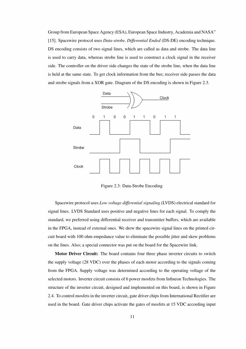
[15]. Spacewire protocol uses Data-strobe, Differential Ended (DS-DE) encoding technique.
DS encoding consists of two signal lines, which are called as data and strobe. The data line
is used to carry data, whereas strobe line is used to construct a clock signal in the receiver
side. The controller on the driver side changes the state of the strobe line, when the data line
is held at the same state. To get clock information from the bus; receiver side passes the data
and strobe signals from a XOR gate. Diagram of the DS encoding is shown in Figure 2.3.
Figure 2.3: Data-Strobe Encoding
Spacewire protocol uses Low voltage differential signaling (LVDS) electrical standard for
signal lines. LVDS Standard uses positive and negative lines for each signal. To comply the
standard, we preferred using differential receiver and transmitter buffers, which are available
in the FPGA, instead of external ones. We drew the spacewire signal lines on the printed cir-
cuit board with 100 ohm empedance value to eliminate the possible jitter and skew problems
on the lines. Also; a special connector was put on the board for the Spacewire link.
Motor Driver Circuit: The board contains four three phase inverter circuits to switch
the supply voltage (28 VDC) over the phases of each motor according to the signals coming
from the FPGA. Supply voltage was determined according to the operating voltage of the
selected motors. Inverter circuit consists of 6 power mosfets from Infineon Technologies. The
structure of the inverter circuit, designed and implemented on this board, is shown in Figure
2.4. To control mosfets in the inverter circuit, gate driver chips from International Rectifier are
used in the board. Gate driver chips activate the gates of mosfets at 15 VDC according input
11
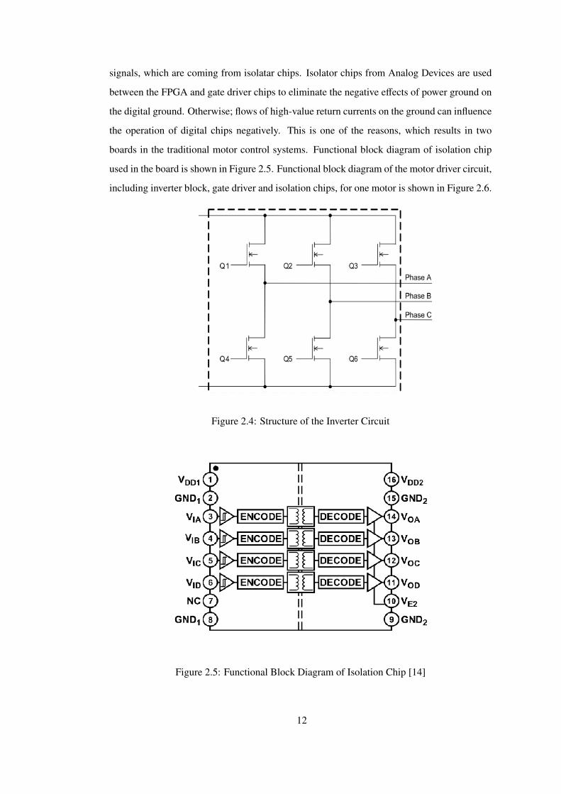
signals, which are coming from isolatar chips. Isolator chips from Analog Devices are used
between the FPGA and gate driver chips to eliminate the negative effects of power ground on
the digital ground. Otherwise; flows of high-value return currents on the ground can influence
the operation of digital chips negatively. This is one of the reasons, which results in two
boards in the traditional motor control systems. Functional block diagram of isolation chip
used in the board is shown in Figure 2.5. Functional block diagram of the motor driver circuit,
including inverter block, gate driver and isolation chips, for one motor is shown in Figure 2.6.
Figure 2.4: Structure of the Inverter Circuit
Figure 2.5: Functional Block Diagram of Isolation Chip [14]
12
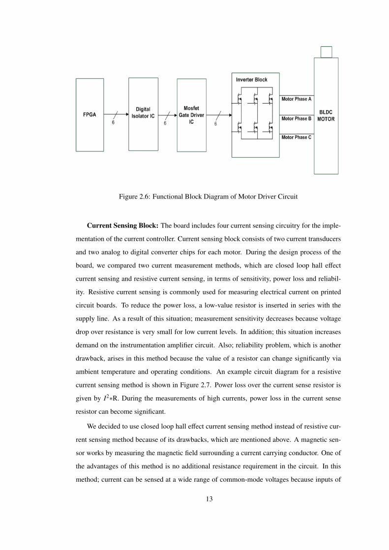
Figure 2.6: Functional Block Diagram of Motor Driver Circuit
Current Sensing Block: The board includes four current sensing circuitry for the imple-
mentation of the current controller. Current sensing block consists of two current transducers
and two analog to digital converter chips for each motor. During the design process of the
board, we compared two current measurement methods, which are closed loop hall effect
current sensing and resistive current sensing, in terms of sensitivity, power loss and reliabil-
ity. Resistive current sensing is commonly used for measuring electrical current on printed
circuit boards. To reduce the power loss, a low-value resistor is inserted in series with the
supply line. As a result of this situation; measurement sensitivity decreases because voltage
drop over resistance is very small for low current levels. In addition; this situation increases
demand on the instrumentation amplifier circuit. Also; reliability problem, which is another
drawback, arises in this method because the value of a resistor can change significantly via
ambient temperature and operating conditions. An example circuit diagram for a resistive
current sensing method is shown in Figure 2.7. Power loss over the current sense resistor is
given by I2∗R. During the measurements of high currents, power loss in the current sense
resistor can become significant.
We decided to use closed loop hall effect current sensing method instead of resistive cur-
rent sensing method because of its drawbacks, which are mentioned above. A magnetic sen-
sor works by measuring the magnetic field surrounding a current carrying conductor. One of
the advantages of this method is no additional resistance requirement in the circuit. In this
method; current can be sensed at a wide range of common-mode voltages because inputs of
13

Figure 2.7: Current measurement with three shunt resistors
these sensors are completely isolated from the output ports of them. Also; there is no need
for an external buffer in the current sensing circuit because output ports of magnetic sensors
are low impedance. Finally; we selected a closed loop hall effect current transducer module
from LEM company. Functional block diagram of current sensor is shown in Figure 2.8. The
measuring range of current sensor is between +50 and -50 amperes above than the estimated
maximum motor currents, which are +30 and -30 amperes. Other parameters of the current
sensor are analyzed in the current controller chapter. To reduce the board size and cost; we
put two current sensors for the A and B phases of each motor. Current of phase C is obtained
in the FPGA by the well known three phase motor current equation that
IC = −(IA + IB) (2.1)
To convert the output of the current sensors into the digital domain; analog to digital con-
verter chips (ADC) are used in the board. We put one single channel ADC chip for the A and
B phases of the motor instead of using a multiplexed ADC chip with two channels for each
14
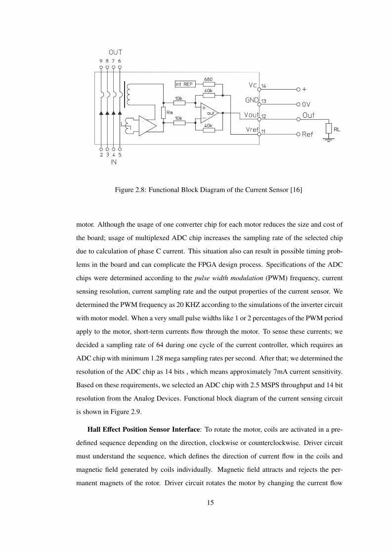
Figure 2.8: Functional Block Diagram of the Current Sensor [16]
motor. Although the usage of one converter chip for each motor reduces the size and cost of
the board; usage of multiplexed ADC chip increases the sampling rate of the selected chip
due to calculation of phase C current. This situation also can result in possible timing prob-
lems in the board and can complicate the FPGA design process. Specifications of the ADC
chips were determined according to the pulse width modulation (PWM) frequency, current
sensing resolution, current sampling rate and the output properties of the current sensor. We
determined the PWM frequency as 20 KHZ according to the simulations of the inverter circuit
with motor model. When a very small pulse widths like 1 or 2 percentages of the PWM period
apply to the motor, short-term currents flow through the motor. To sense these currents; we
decided a sampling rate of 64 during one cycle of the current controller, which requires an
ADC chip with minimum 1.28 mega sampling rates per second. After that; we determined the
resolution of the ADC chip as 14 bits , which means approximately 7mA current sensitivity.
Based on these requirements, we selected an ADC chip with 2.5 MSPS throughput and 14 bit
resolution from the Analog Devices. Functional block diagram of the current sensing circuit
is shown in Figure 2.9.
Hall Effect Position Sensor Interface: To rotate the motor, coils are activated in a pre-
defined sequence depending on the direction, clockwise or counterclockwise. Driver circuit
must understand the sequence, which defines the direction of current flow in the coils and
magnetic field generated by coils individually. Magnetic field attracts and rejects the per-
manent magnets of the rotor. Driver circuit rotates the motor by changing the current flow
15
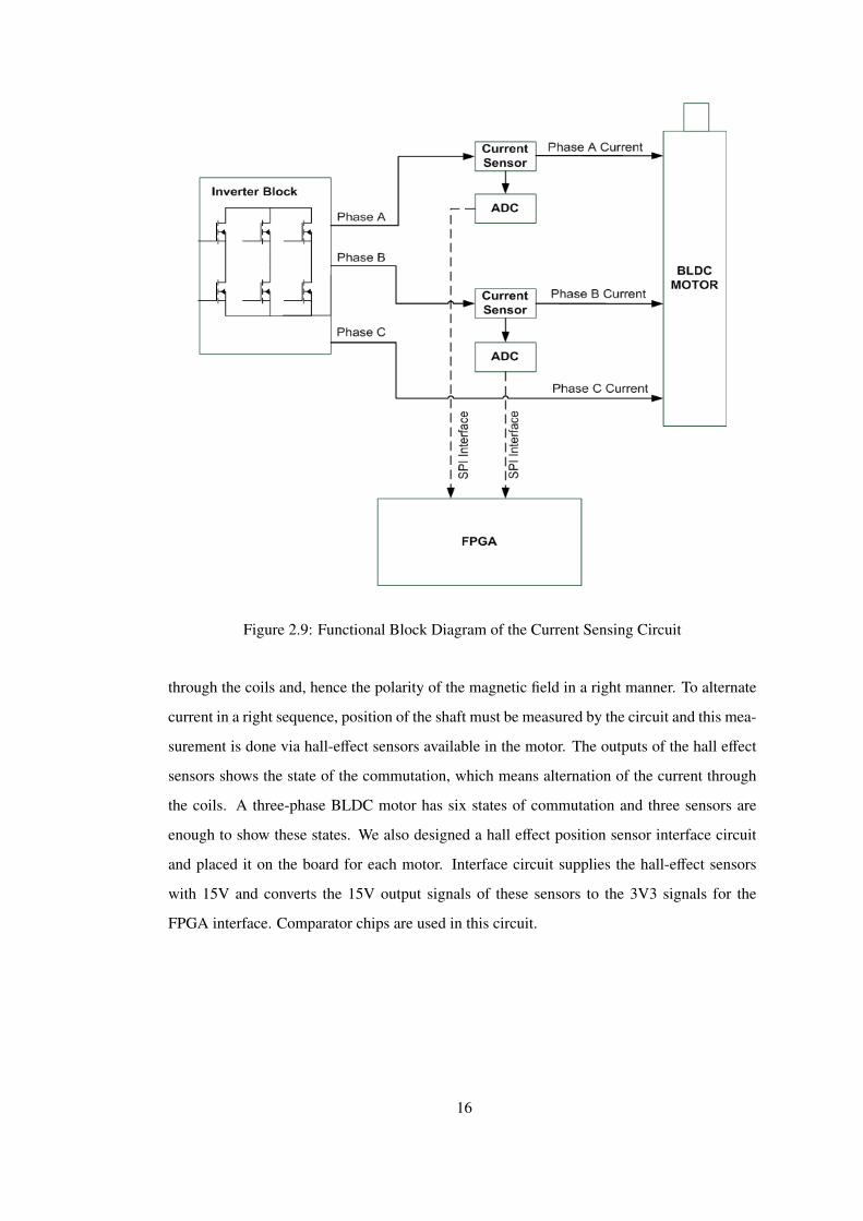
Figure 2.9: Functional Block Diagram of the Current Sensing Circuit
through the coils and, hence the polarity of the magnetic field in a right manner. To alternate
current in a right sequence, position of the shaft must be measured by the circuit and this mea-
surement is done via hall-effect sensors available in the motor. The outputs of the hall effect
sensors shows the state of the commutation, which means alternation of the current through
the coils. A three-phase BLDC motor has six states of commutation and three sensors are
enough to show these states. We also designed a hall effect position sensor interface circuit
and placed it on the board for each motor. Interface circuit supplies the hall-effect sensors
with 15V and converts the 15V output signals of these sensors to the 3V3 signals for the
FPGA interface. Comparator chips are used in this circuit.
16
2.1.1 Structure of the FPGA Design
Within the scope of this study; FPGA design is completely done by me. The BLDC motor
controller was designed and implemented in the FPGA within the scope of this thesis work.
Firstly; position and current controllers are designed and simulated in the Matlab platform.
After the verification of designs on the simulation platform; current and position controllers
are coded in Very High Speed Integrated Circuit Hardware Description Language (VHDL)
and C (programming language), respectively. By this way; position and current controllers
can operate in parallel and, hence sampling, update rates of the controllers can become higher
compared to the implementations in the processor. Also; implementation of current controller
in VHDL increases the flexibility because VHDL modules can be implemented in any FPGA
model. This situation removes the chip obsolescence problem, which is an important risk for
the continuity of the electronic systems. Microblaze soft processor reduced the integration
and testing periods of the VHDL modules. In addition; usage of soft processor in the FPGA
provides flexibility and configurability for the system. For example; electronic board designed
for this work can be adapted to another board or system via changing the packet structure,
coded in C programming language, for the UART protocol. In addition; this system can be
converted to an Application Specific Integrated Circuit (ASIC) chip especially for increasing
the reliability of the system via netlist files generated automatically by the code synthesizer.
In this work; Xilinx ISE (Integrated Synthesis Enviroment) program was used for debugging
and implementation of VHDL modules and Xilinx Platform Studio program was used for
the design and implementation of Microblaze soft processor. To simulate VHDL modules;
Modelsim, which is an advanced simulation and debugging tool for ASIC and FPGA projects
provided by Mentor Graphics, is used in this work. Functional block diagram of the FPGA
design is shown in Figure 2.10.
17

Figure 2.10: Functional Block Diagram of the FPGA Design
18
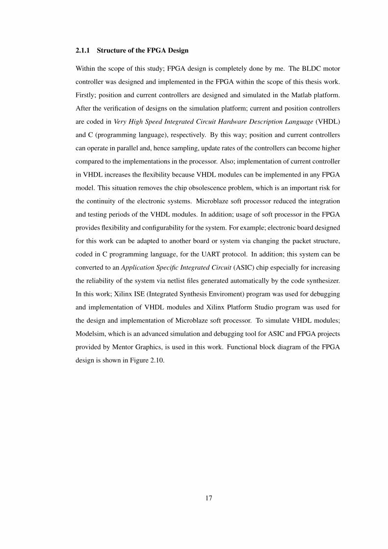
FPGA utilization of the motor control system in Figure 2.10 is evaluated and the result is
listed in Table 2.1
Table 2.1: Summary of the FPGA utilization characteristics for the motor control system
IP Number of Number of Number ofSlices LUTs BRAMs
Microblaze Soft 2128 out of 27648 3927 out of 55296 40 out of 96Processor IP 8% 7% 42%Four Current 6050 out of 27648 10721 out of 55296 8 out of 96Controllers + 22% 20% 8%
Bus Controller +
Spacewire ControllerExternal Memory 629 out of 27648 897 out of 55296 —–
Controller 2% 1% —–UART 16750 357 out of 27648 605 out of 55296 —–
Controller 1% 1% —–Encoder 327 out of 27648 344 out of 55296 —–
Glue Logic 1% 1% —–SPI Flash 184 out of 27648 256 out of 55296 —–Controller 1% 1% —–Microblaze 296 out of 27648 509 out of 55296 —–
PLB 1% 1% —–9996 out of 27648 509 out of 55296 48 out of 96
Total 37% 32% 50%
Microblaze Soft Processor: The MicroBlaze embedded processor soft core is a reduced
instruction set computer (RISC) optimized for implementation in Xilinx FPGAs. Microblaze
is implemented entirely in the general-purpose memory and the logic fabric of Xilinx FPGAs.
Microblaze processor core includes thirty-two 32-bit general purpose registers, 32-bit instruc-
tion word, 32-bit address bus and single issue pipeline. Besides these fixed features; processor
can be configured for additional functionality such as barrel shifter, hardware multiplier and
divider, floating point unit, memory management unit and etc. Microblaze processor core
versions are available in the market and version 7.00 is used in this study. Xilinx EDK is the
hardware development platform for the Microblaze processor core based systems and Xilinx
SDK is the software development platform for the Microblaze core. Functional block diagram
of the Microblaze soft processor core is shown in Figure 2.11.
Pipeline Architecture: Microblaze core instruction execution is pipelined. Each pipeline
stage takes one clock cycle to complete and the completion time of an instruction is equal to
the pipeline stages. A few instructions require multiple clock cycles in the execute stage to
19

Figure 2.11: Functional Block Diagram of the Microblaze Processor Core [17]
complete. This is achieved by stalling the pipeline. When area optimization is enabled, the
pipeline is divided into three stages to minimize hardware cost. Three stage pipeline structure
is shown in Figure 2.12. However; the pipeline is divided into five stages to maximize the
performance when area optimization is disabled.
Memory Architecture: Microblaze processor core is implemented with a Harvard Mem-
ory architecture; instruction and data accesses are done in separate address spaces [17]. Each
address space can handle up to 4 GB of instructions and data memory respectively. Mi-
croblaze processor core’s instruction and data interfaces are 32 bits wide and use big endian,
bit-reversed format. Separate accesses to I/O and memory are not supported in the archi-
tecture of the processor. The processor has three interfaces for the memory accesses, which
are Local Memory Bus (LMB), (Processor Local Bus) (PLB) and Xilinx Cache Link (XCL).
LMB is a synchronous bus and used for gaining access to block rams available in the FPGA.
Xilinx Cache Link is a high performance bus and used for gaining access to cache memories.
20

Figure 2.12: Three Stage Pipeline Structure of the Microblaze Core [17]
Cache memories are used for connection between the core and external memory chip. PLB is
a system memory mapped transaction bus with master/slave capability. In this study; we used
the local memory bus and Xilinx cache link to access BRAMs and external memory chip,
SRAM, respectively. In addition; peripheral local bus (PLB) is used for connection of custom
VHDL modules to the processor core.
External Memory Controller: To control SRAM chip available in the board; Xilinx
generic external memory controller is connected to the Microblaze soft processor core via
cache link and peripheral local bus. The Xilinx EDK development platform provides some
ready modules for different applications. The generic external memory controller is one of
them and it can control SDRAM, SRAM and FLASH chips. However; it is used for the
SRAM chip only.
UART Controller: A UART controller is decided to be implemented in the FPGA in-
stead of using controller chips on the board because it reduces the cost and the size of the
board. Also; it adds configurability and flexibility to the system. After that; we looked for an
appropriate VHDL controller and decided to use UART 16750 controller, downloadable from
the website of opencores (6). The Xilinx EDK platform has a UART 16550 controller, but it
can be used after purchasing. UART 16750 controller has some advantages according to the
UART 16550 in terms of FIFO size and loopback test modes. The UART 16750 controller is
connected to the Microblaze processor core via peripheral local bus.
SPI Flash Controller: To control the SPI flash chip; a VHDL controller module was
downloaded from the website of opencores and connected to the Microblaze processor core by
the peripheral local bus. This module is used as glue logic between the Microblaze processor
and flash chip. Controller communicates with the flash chip via Serial Peripheral Interface
(SPI) according to the commands coming from the Microblaze processor.
6 To get more information about the opencores visit www.opencores.org
21

Current Controller: As mentioned in the previous parts; current controller is coded in
VHDL and implemented in the FPGA. The same controller module is used for each motor.
To connect current controller of each motor and Spacewire controller with the Microblaze
soft processor core; a bus controller is coded in VHDL and connected to the processor. Bus
controller module directs the commands and configuration parameters to the related controller
and gets information from the controllers according to the request of the processor. Data
exchange between the bus controller and processor is done via registers. Spacewire controller
is connected to the bus controller instead of connecting to the processor directly. By this way;
controller module can be used in a different system as a whole. However; packet controller of
the Spacewire protocol must be reimplemented when the spacewire controller is connected to
the processor directly. Design and implementation of the controller are explained in detail in
Chapter 3.
Position Controller: Position controller is coded and implemented in the Microblaze soft
processor in the FPGA. Design and implementation of the position controller are explained
in detail in Chapter 4.
22
2.2 Graphical User Interface Design
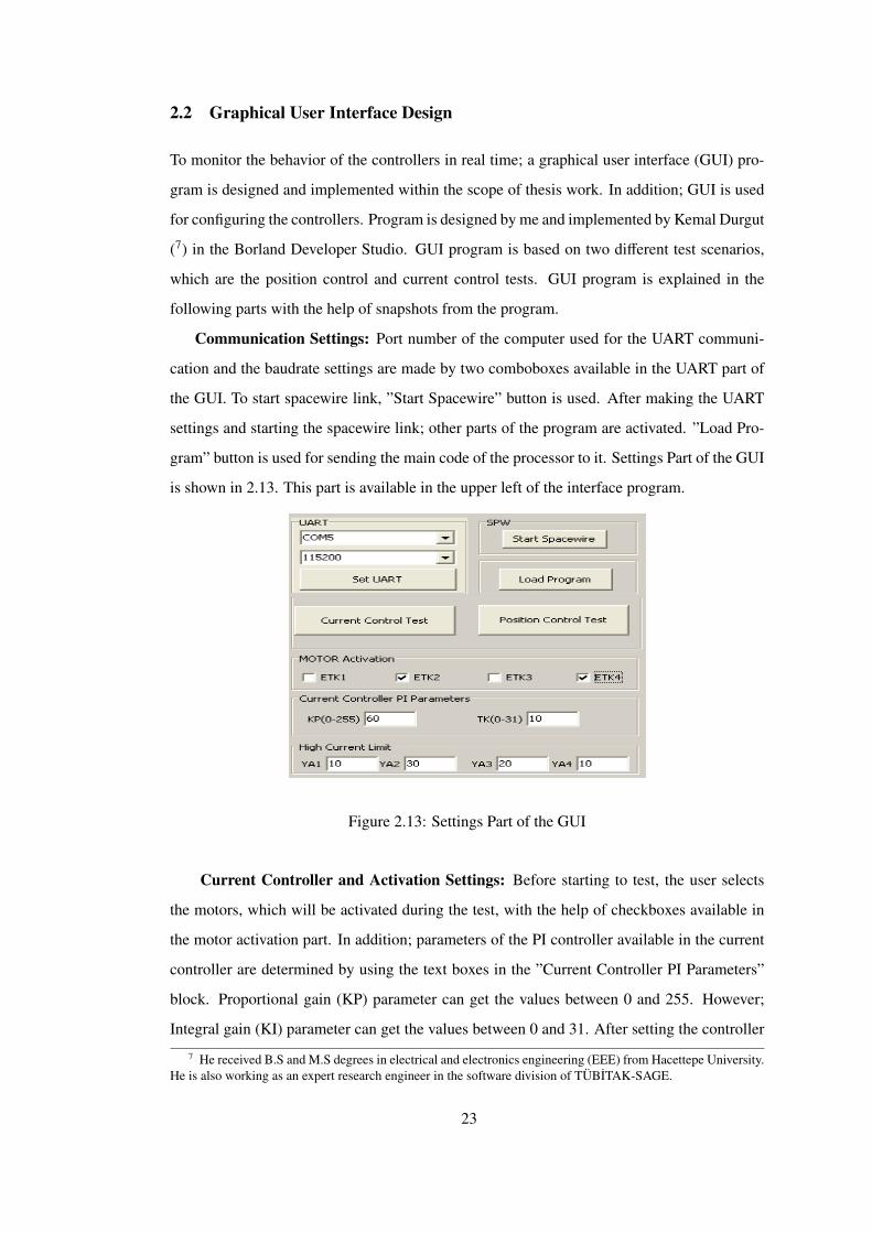
To monitor the behavior of the controllers in real time; a graphical user interface (GUI) pro-
gram is designed and implemented within the scope of thesis work. In addition; GUI is used
for configuring the controllers. Program is designed by me and implemented by Kemal Durgut
(7) in the Borland Developer Studio. GUI program is based on two different test scenarios,
which are the position control and current control tests. GUI program is explained in the
following parts with the help of snapshots from the program.
Communication Settings: Port number of the computer used for the UART communi-
cation and the baudrate settings are made by two comboboxes available in the UART part of
the GUI. To start spacewire link, ”Start Spacewire” button is used. After making the UART
settings and starting the spacewire link; other parts of the program are activated. ”Load Pro-
gram” button is used for sending the main code of the processor to it. Settings Part of the GUI
is shown in 2.13. This part is available in the upper left of the interface program.
Figure 2.13: Settings Part of the GUI
Current Controller and Activation Settings: Before starting to test, the user selects
the motors, which will be activated during the test, with the help of checkboxes available in
the motor activation part. In addition; parameters of the PI controller available in the current
controller are determined by using the text boxes in the ”Current Controller PI Parameters”
block. Proportional gain (KP) parameter can get the values between 0 and 255. However;
Integral gain (KI) parameter can get the values between 0 and 31. After setting the controller
7 He received B.S and M.S degrees in electrical and electronics engineering (EEE) from Hacettepe University.He is also working as an expert research engineer in the software division of TUBITAK-SAGE.
23

parameters, user should enter the high current limit values of each motor to the text boxes
available in the ”High Current Limit” part of the program. High current limits of each motor
can be set independently.
Current Control Test Patterns: After setting the current controller’s parameters, current
patterns, which will be applied to the motor during the test, can be created via the current
control test parameters window. This window appears when the ”current control test” button
is activated. Test patterns can be created independently for each motor. The current control
test parameters window of the GUI program is shown in Figure 2.14. User sets the amplitude
of the current command in terms of mili-amperes by entering the desired value to the text
box called ”Current Comm”. Duration of the command is determined according to the value
in the ”Comm Duration” text box. After these steps; command can be shown in the graph
by activating the ”add” button. If user wants to remove the last command, ”subtract” button
must be activated. The value of the textbox called as ”repeat count” determines how many
times the current pattern repeats. The default value of this box is zero, which means infinity
repetition.
Figure 2.14: Current Control Test Parameters Window of the GUI
24
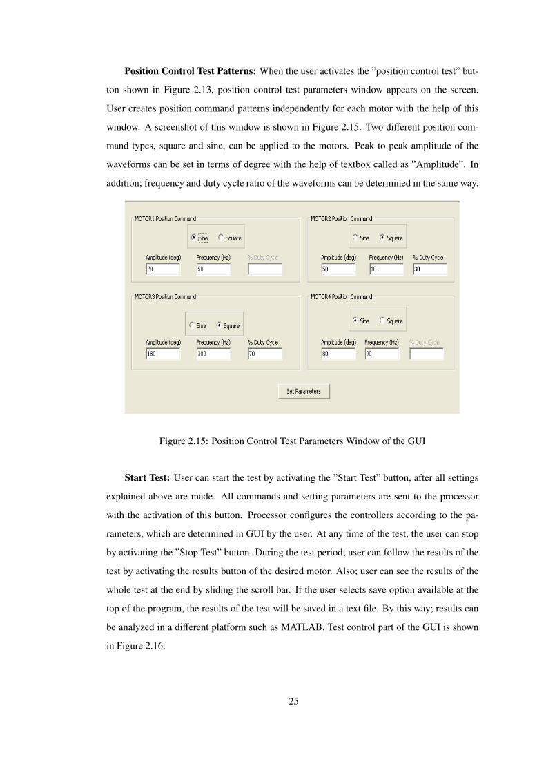
Position Control Test Patterns: When the user activates the ”position control test” but-
ton shown in Figure 2.13, position control test parameters window appears on the screen.
User creates position command patterns independently for each motor with the help of this
window. A screenshot of this window is shown in Figure 2.15. Two different position com-
mand types, square and sine, can be applied to the motors. Peak to peak amplitude of the
waveforms can be set in terms of degree with the help of textbox called as ”Amplitude”. In
addition; frequency and duty cycle ratio of the waveforms can be determined in the same way.
Figure 2.15: Position Control Test Parameters Window of the GUI
Start Test: User can start the test by activating the ”Start Test” button, after all settings
explained above are made. All commands and setting parameters are sent to the processor
with the activation of this button. Processor configures the controllers according to the pa-
rameters, which are determined in GUI by the user. At any time of the test, the user can stop
by activating the ”Stop Test” button. During the test period; user can follow the results of the
test by activating the results button of the desired motor. Also; user can see the results of the
whole test at the end by sliding the scroll bar. If the user selects save option available at the
top of the program, the results of the test will be saved in a text file. By this way; results can
be analyzed in a different platform such as MATLAB. Test control part of the GUI is shown
in Figure 2.16.
25
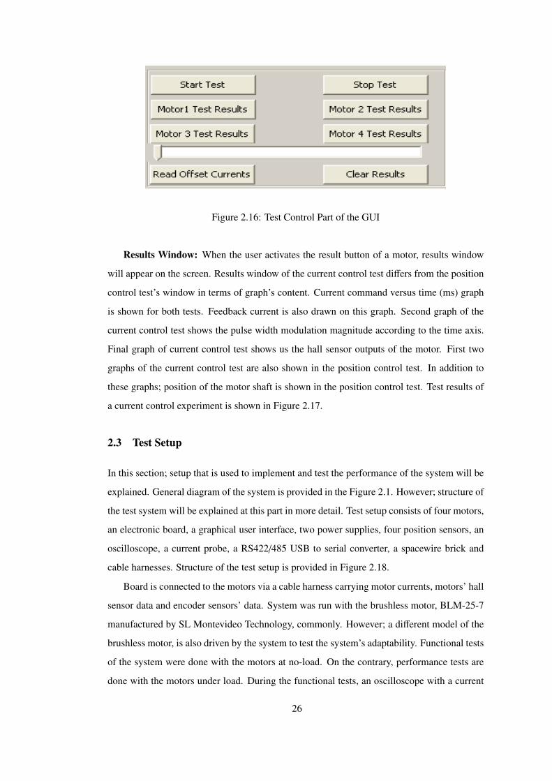
Figure 2.16: Test Control Part of the GUI
Results Window: When the user activates the result button of a motor, results window
will appear on the screen. Results window of the current control test differs from the position
control test’s window in terms of graph’s content. Current command versus time (ms) graph
is shown for both tests. Feedback current is also drawn on this graph. Second graph of the
current control test shows the pulse width modulation magnitude according to the time axis.
Final graph of current control test shows us the hall sensor outputs of the motor. First two
graphs of the current control test are also shown in the position control test. In addition to
these graphs; position of the motor shaft is shown in the position control test. Test results of
a current control experiment is shown in Figure 2.17.
2.3 Test Setup
In this section; setup that is used to implement and test the performance of the system will be
explained. General diagram of the system is provided in the Figure 2.1. However; structure of
the test system will be explained at this part in more detail. Test setup consists of four motors,
an electronic board, a graphical user interface, two power supplies, four position sensors, an
oscilloscope, a current probe, a RS422/485 USB to serial converter, a spacewire brick and
cable harnesses. Structure of the test setup is provided in Figure 2.18.
Board is connected to the motors via a cable harness carrying motor currents, motors’ hall
sensor data and encoder sensors’ data. System was run with the brushless motor, BLM-25-7
manufactured by SL Montevideo Technology, commonly. However; a different model of the
brushless motor, is also driven by the system to test the system’s adaptability. Functional tests
of the system were done with the motors at no-load. On the contrary, performance tests are
done with the motors under load. During the functional tests, an oscilloscope with a current
26

Figure 2.17: Test Results of a Current Control Experiment
27
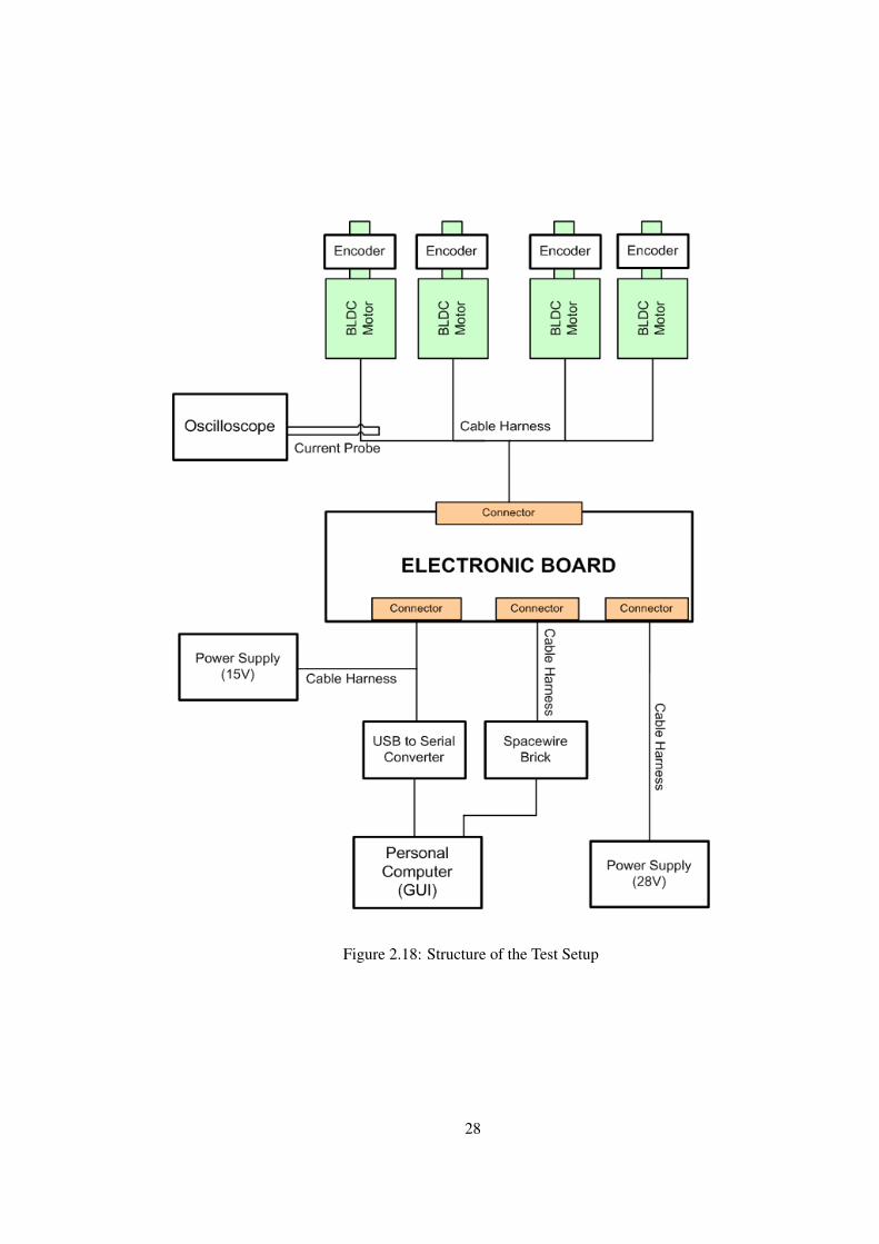
Figure 2.18: Structure of the Test Setup
28

probe is used for verifying the monitor part of the graphical user interface program. Current
flowing on three phases of each motor was measured and monitored on the oscilloscope screen
with the help of current probe. Comparisons between the graphical results of the oscilloscope
and GUI program were made during the functional tests. A Spacewire brick manufactured
by Star-Dundee was used for transferring the outputs of the controllers from board to com-
puter via Spacewire protocol. To reduce signal attenuation, crosstalk and skew problems, a
specific cable harness was used between the Spacewire brick and board. An overview of the
SpaceWire Brick hardware architecture is shown in Figure 2.19.
Figure 2.19: An Overview of the SpaceWire Brick Hardware Architecture [18]
A USB to serial converter manufactured by MOXA was used as a translator between the
RS422 and USB signals because personal computers don’t have a port compatible with RS422
or RS485 electrical standard. Graphical user interface program sends setting parameters and
test patterns to the board via UART protocol over the RS422 electrical interface. A single
cable harness is used between the board, USB to serial converter module and power supply
providing 15V. Digital electronic part of the board is supplied from 15V and other parts are
supplied from 28V.
29

CHAPTER 3
DESIGN AND IMPLEMENTATION OF CURRENT
CONTROLLER
In this study, a current controller is designed and implemented in FPGA to control motor
torque. Torque control means controlling the motor current based on the following approxi-
mation that
Tm = Kt.i (3.1)
Tm : Motor torque, N-m
Kt : Motor torque constant, N-m/A
i : Motor current, A
The performance of the current control system directly affects the position control loop. If
the current control loop (inner control loop) cannot trace the current commands coming from
the position controller efficiently, position tracking performance of the position controller will
degrade dramatically. In the scope of this study, current controller was tested alone firstly to
monitor the tracking performance of it. After that; performance of the controller was tested
with the position controller loop because the current controller cannot work as stand alone in
the system.
In the beginning of design stage; current controller was designed at the conceptual level
and simulated in the simulink platform of the MATLAB program. After the conceptual model
was verified on the simulation platform, the controller was coded in VHDL. VHDL modules
of the current controller were simulated in the MODELSIM simulation program during the
coding process. After the completion of these stages, controller was implemented in the
FPGA and tested on the board.
30

3.1 Current Controller Design
Current controller, which is designed and implemented in the scope of this study, consists
of mainly current acquisition, current accumulator, average current calculation, offset detec-
tion, PI (Proportional Integral) controller, commutation VHDL modules and current sensing,
inverter circuits. VHDL modules are implemented in the FPGA, but current sensing and in-
verter circuits are implemented on the printed circuit board. Functional block diagram of the
current controller is shown in Figure 3.1. In the current acquisition part; digital output of the
current sensing circuit is taken and scaled for the other parts of the controller. Phase A , phase
B, phase C current read and phase detection blocks shown in the Figure 3.1 compose the
current acquisition part of the controller. The detailed description of this part is explained in
the following sections. In the current integrator block, the currents of the motor are summed
throughout the one operating cycle of the controller for calculating the average motor current.
In the average current calculation module, average motor current is calculated by division of
the current sum with the sample count.
Magnetic current sensors have an electrical offset voltage, which affects the performance
of the controller, at the output of them. The electrical offset voltage of the magnetic sensors
belonging to the same company can vary between the products of the same model. To elimi-
nate the effects of that, offset detection module was designed and implemented in the FPGA.
Controller topology of the current controller is determined as PI according to the MATLAB
simulations and implementation difficulty. Design and implementation of the PI controller are
explained in detail in the following parts. The output of the PI controller is scaled in the pulse
width generator module for driving the motor commutation control module. Motor commu-
tation module drives the mosfet gate drivers according to the input, activation command, hall
sensor outputs of the motor and output of the high current detection block. Aim of the high
current detection block is to limit motor currents at a level. If we do not use a current limiter in
the controller, possible damages can occur on the supply and printed circuit board especially
in times of testing.
Current controller was implemented in VHDL after the verification of the design in the
MATLAB platform. Structure of the current controller VHDL module design is shown in the
Figure 3.2.
31
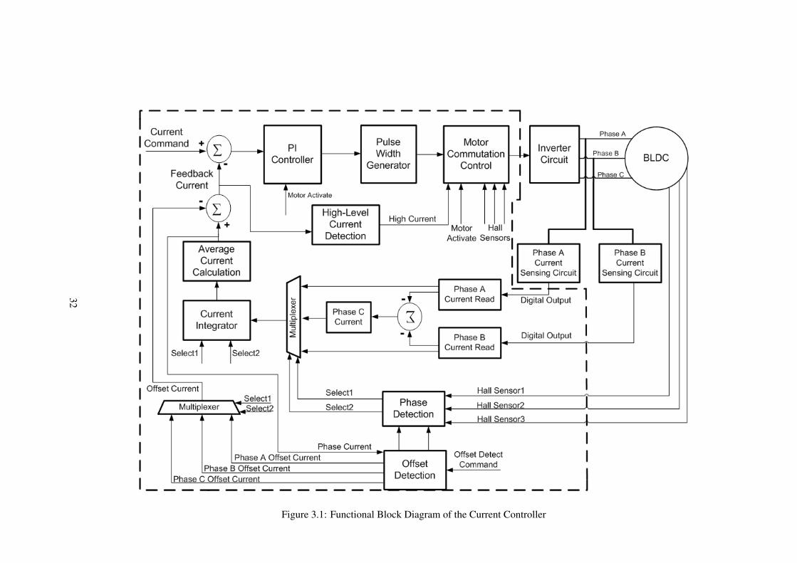
Figure 3.1: Functional Block Diagram of the Current Controller
32
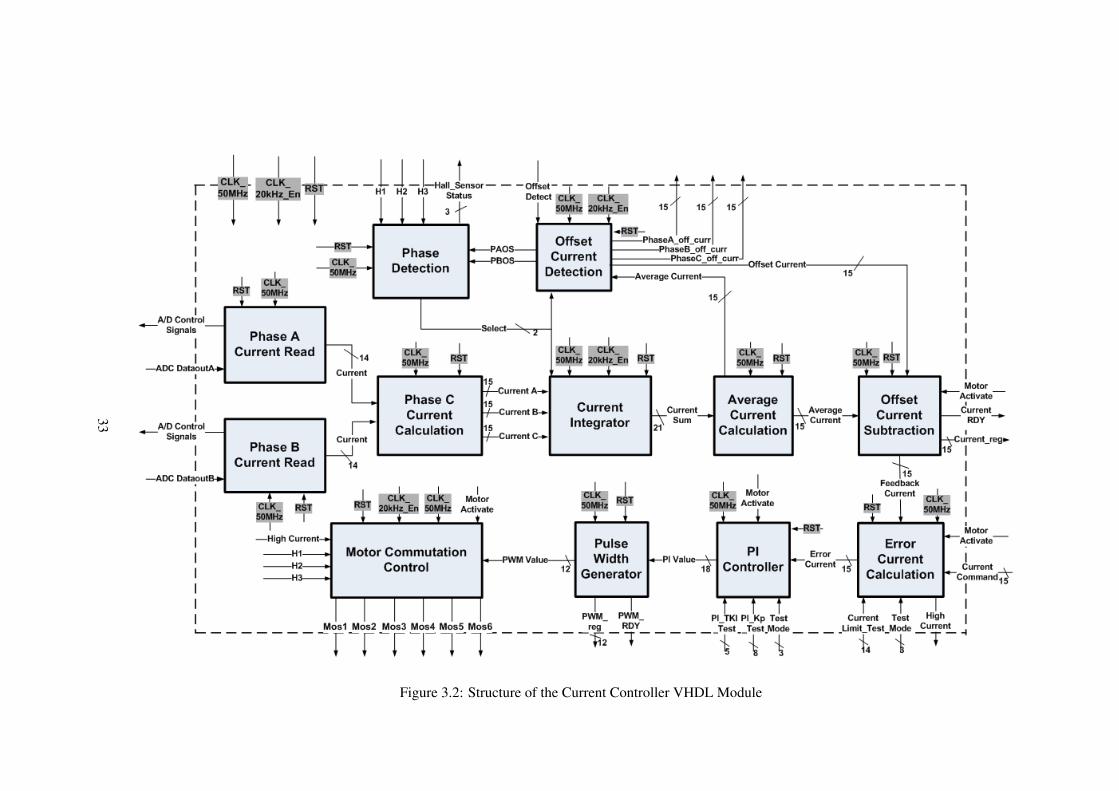
Figure 3.2: Structure of the Current Controller VHDL Module
33
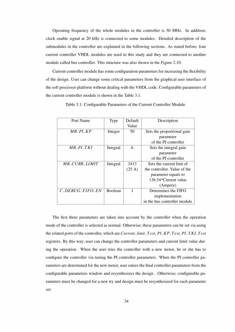
Operating frequency of the whole modules in the controller is 50 MHz. In addition;
clock enable signal at 20 kHz is connected to some modules. Detailed description of the
submodules in the controller are explained in the following sections. As stated before; four
current controller VHDL modules are used in this study and they are connected to another
module called bus controller. This structure was also shown in the Figure 2.10.
Current controller module has some configuration parameters for increasing the flexibility
of the design. User can change some critical parameters from the graphical user interface of
the soft processor platform without dealing with the VHDL code. Configurable parameters of
the current controller module is shown in the Table 3.1.
Table 3.1: Configurable Parameters of the Current Controller Module
Port Name Type Default DescriptionValue
MB−PI−KP Integer 50 Sets the proportional gainparameter
of the PI controllerMB−PI−T KI Integral 6 Sets the integral gain
parameterof the PI controller
MB−CURR−LIMIT Integral 3413 Sets the current limt of(25 A) the controller. Value of the
parameter equals to136.54*Current value
(Ampere)C−DEBUG−FIFO−EN Boolean 1 Determines the FIFO
implementationin the bus controller module
The first three parameters are taken into account by the controller when the operation
mode of the controller is selected as normal. Otherwise; these parameters can be set via using
the related ports of the controller, which are Current−limit−Test, PI−KP−Test, PI−T KI−Test
registers. By this way; user can change the controller parameters and current limit value dur-
ing the operation. When the user tries the controller with a new motor, he or she has to
configure the controller via tuning the PI controller parameters. When the PI controller pa-
rameters are determined for the new motor, user enters the final controller parameters from the
configurable parameters window and resynthesizes the design . Otherwise; configurable pa-
rameters must be changed for a new try and design must be resynthesized for each parameter
set.
34

Configurable parameters window of the current controller on the EDK platform is shown
in the Figure 3.3. Last parameter, which is C−DEBUG−FIFO−EN, can be used for the low
valued FPGAs in terms of the source. When the user does not want to get feedback from
the controller, he or she can set this parameter to zero. By this way; block ram modules
and the feedback controller logic are not synthesized and the utilization ratio falls ten percent
approximately.
Figure 3.3: Configurable parameters window of the current controller on the EDK platform
Input, output ports of the current controller module, which are connected to the bus con-
troller module, are shown in the Table 3.2 and 3.3. Some ports of the current controller does
not affect the operation of the controller, but they are used for the monitoring operation. Bus
controller module takes the feedback data from the controllers by using these ports, which are
explained in detail in the bus controller section.
35

Table 3.2: Input, Output ports of the Current Controller Module
Port Name Width Direction DescriptionCLK−50MHZ 1 bit In Clock Input 50 MHz
RST 1 bit In Module Active High Reset SignalCLK−20kHz−en 1 bit In Clock Enable Signal at 20 kHzO f f set−Detect 1 bit In Initiates the offset current detection
operationCurrent−Command 14 bits In Current Command; most significant
bit representsthe current direction. 0 means + ,
1 means -Motor−Activate 1 bit In Activates the Motor
H1 1 bit In First Hall Sensor of the MotorH2 1 bit In Second Hall Sensor of the MotorH3 1 bit In Third Hall Sensor of the Motor
ADC−DataoutA 1 bit In Data output of the ADC chip,which is connected to the phase A
of the motorADC−DataoutB 1 bit In Data output of the ADC chip,
which is connected to the phase Bof the motor
ADC−S CKA 1 bit Out Serial clock port of the ADC chip,which is connected to the phase A
of the motorADC−S CKB 1 bit Out Serial clock port of the ADC chip,
which is connected to the phase Bof the motor
ADC−CNVA 1 bit Out Initiates the Analog to DigitalConversion of the Phase A ADC chip
ADC−CNVB 1 bit Out Initiates the Analog to DigitalConversion of the Phase B ADC chip
Mos1 1 bit Out Drives the phase A mosfet,of which drain is connected
to the supplyMos2 1 bit Out Drives the phase A mosfet,
of which source is connectedto the ground
Mos3 1 bit Out Drives the phase B mosfet,of which source is connected
to the supplyMos4 1 bit Out Drives the phase B mosfet,
of which source is connectedto the ground
36

Table 3.3: Continuation of the Input, Output ports of the Current Controller Module
Mos5 1 bit Out Drives the phase C mosfet,of which source is connected
to the supplyMos6 1 bit Out Drives the phase C mosfet,
of which source is connectedto the ground
High−current 1 bit Out Set to 1 if feedback current isgreater than current limit
Current−limit−Test 14 bits In Sets the current limit valueTest−Mode 3 bits In Determines the operation mode
(Test, Normal) of the controllerPI−KP−Test 8 bits In Sets the proportional gain parameter
of the PI controllerPI−T KI−Test 5 bits In Sets the integral gain parameter
of the PI controllerCurrent−RDY 1 bit Out Shows the new feedback current is
calculated and the register is readyCurrent−reg 15 bits Out Holds the feedback currentPWM−RDY 1 bit Out Shows the new pulse width value is
calculated and the register is readyPWM−reg 12 bits Out Holds the PWM value
PhaseA−o f f−curr 15 bits Out Holds the offset current valueof the Phase A
PhaseB−o f f−curr 15 bits Out Holds the offset current valueof the Phase B
PhaseC−o f f−curr 15 bits Out Holds the offset current valueof the Phase C
Hall−sensor−status 3 bits Out Holds the status of the motor hallsensor signals
Operation of the current controller VHDL module could be observable from the flowchart
of the module, shown in the Figure 3.4. At the beginning; module checks the motor activation
command continuously. If the offset detection command comes before the motor activation
command, offset detection operation is enabled. Providing that the motor activation command
is enabled during the offset detection operation, controller stops the operation and checks the
test mode of the controller. According to the status of the test mode register, Kp, T Ki and
current limit values are determined. After that; module starts to sample the phase currents
when the rising edge of the 20 kHz enable signal is catched. In addition to the sampling
operation; module detects the active phase of the motor and activates the mosfets.
37
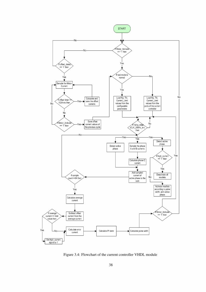
Figure 3.4: Flowchart of the current controller VHDL module
38
Module gets and accumulates 64 current samples, which are taken from the active phase
of the motor. In order to calculate feedback current, averaging operation is applied to the sum
term. Actually; calculated average current includes some errors due to the current sensors
as stated in the previous parts. To eliminate these errors; predetermined offset current is
subtracted from the average current. After that; error current is calculated via subtracting the
feedback current from the error current. This error current is given to the PI controller as
input and output of the PI controller is used by the pulse width detection module in order to
calculate pulse width. This pulse width value will be used by the commutation module in the
next cycle.
3.1.1 Current Acquisition
To measure the motor phase currents, a current sensing circuit is designed and implemented
on the board. Board includes two current sensing circuits for the A and B phases of each
motor. However; phase C current is obtained in the FPGA by the well known three phase
motor current equation that
IC = −(IA + IB) (3.2)
An analog to digital converter chip is used in the output stage of the sensing circuit. To
communicate with the ADC chips, a driver was coded in VHDL and implemented in the
FPGA. The phase A, phase B current read modules shown in the Figure 3.2 get the output
of the ADC chips. Output registers of these modules are connected to the inputs ports of
the phase C current calculation module. Structure of the current acquisition block is shown
in the Figure 3.5. Output port of the Phase C current calculation module, whose name is
ADC−Read, initiates the phase A and B current read modules. When the reading operation
is completed, modules set the RDY port to 1 for one clock cycle. In addition; output current
registers of the phase A and B current read modules are get by the phase C current calculation
module. After that; phase C current module obtains the current of the phase C current by
using the output registers of the phase A and phase B current read modules.
39
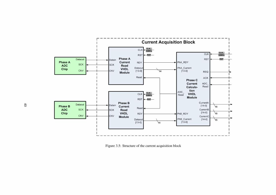
Figure 3.5: Structure of the current acquisition block
40
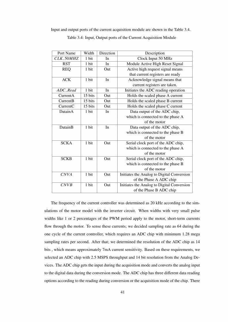
Input and output ports of the current acquisition module are shown in the Table 3.4.
Table 3.4: Input, Output ports of the Current Acquisition Module
Port Name Width Direction DescriptionCLK−50MHZ 1 bit In Clock Input 50 MHz
RST 1 bit In Module Active High Reset SignalREQ 1 bit Out Active high request signal means
that current registers are readyACK 1 bit In Acknowledge signal means that
current registers are taken.ADC−Read 1 bit In Initiates the ADC reading operationCurrentA 15 bits Out Holds the scaled phase A currentCurrentB 15 bits Out Holds the scaled phase B currentCurrentC 15 bits Out Holds the scaled phase C currentDatainA 1 bit In Data output of the ADC chip,
which is connected to the phase Aof the motor
DatainB 1 bit In Data output of the ADC chip,which is connected to the phase B
of the motorSCKA 1 bit Out Serial clock port of the ADC chip,
which is connected to the phase Aof the motor
SCKB 1 bit Out Serial clock port of the ADC chip,which is connected to the phase B
of the motorCNVA 1 bit Out Initiates the Analog to Digital Conversion
of the Phase A ADC chipCNVB 1 bit Out Initiates the Analog to Digital Conversion
of the Phase B ADC chip
The frequency of the current controller was determined as 20 kHz according to the sim-
ulations of the motor model with the inverter circuit. When widths with very small pulse
widths like 1 or 2 percentages of the PWM period apply to the motor, short-term currents
flow through the motor. To sense these currents; we decided sampling rate as 64 during the
one cycle of the current controller, which requires an ADC chip with minimum 1.28 mega
sampling rates per second. After that; we determined the resolution of the ADC chip as 14
bits , which means approximately 7mA current sensitivity. Based on these requirements, we
selected an ADC chip with 2.5 MSPS throughput and 14 bit resolution from the Analog De-
vices. The ADC chip gets the input during the acquisition mode and converts the analog input
to the digital data during the conversion mode. The ADC chip has three different data reading
options according to the reading during conversion or the acquisition mode of the chip. There
41

is the option to read during conversion, to split the read across acquisition and conversion and
to read during acquisition.
Reading During Conversion: When reading during the conversion (n), conversion re-
sults are for the previous (n-1) conversion. Reading should occur only up to tdata ( maximum
data read time during conversion process) and, because this time is limited, the host must use
a fast clock. The required clock frequency is calculated with the following equation that
Clock f requency ≥Numbero fClockEdges
Tdata(3.3)
Number of Clock Edges : 14
Tdata : 290 ns for Normal Mode (2 MSPS), 190 ns for Turbo Mode (2.5 MSPS)
According to the ADC clock frequency equation; minimum required frequency must be
48.3 MHZ for normal mode, 73.7 MHZ for turbo mode. We operate the ADC chip in normal
mode because we sample current at 1.28 MSPS, which is under the limit of normal mode.
Split Reading: To allow for a slower clock frequency, there is the option of a split read,
where data access starts at the current acquisition (n) and spans into the conversion (n). Con-
version results are for the previous (n-1) conversion. According to the calculation for 50 MHZ
clock frequency, required clock edge during the conversion cycle must be 9 for Turbo mode.
However, required clock edges must be 14 at 50 MHZ during the conversion cycle for the
normal mode of ADC chip.
Reading during acquisation: When reading during acquisition (n), conversion results
are for the previous (n-1) conversion. In this mode; chip can not be operated in the turbo
mode, so 2.5 MSPS throughput can not be achieved.
We decided to run the digital interface of the ADC chip at 50 MHZ in the split reading
mode because reading of all data during the conversion mode requires higher clock rates such
as 48 MHz for 2.0 MSPS. In addition; maximum throughput of the chip can not be achieved
when the all data are read during the acquisition mode. Because of these reasons; we run
chip at 50 MHz and 10 bits data are read during the conversion state. The rest of the data (4
bits) are read during the acquisition mode. Driver code is implemented according to timing
diagram shown in the Figure 3.6.
Motor phase currents are sampled 65 times at one operating cycle. However; we take
into account 64 of them because the first current sample belongs to the previous cycle due
to the ADC reading technique. So; one sampling period must be 50 us / 65, which equals to
769.2 nanoseconds. If we take into account calculation time of other operations, this sampling
42

Figure 3.6: Serial Interface Timing Diagram of AD7944 chip [19]
period should be less than the specified time 769.2 ns. As a result; we determined the sampling
period as 760 ns by considering the required calculation time of other operations. According
to the 760 ns sampling period time; 600 ns will be left for the other calculations. Simulation
of ADC driver code for one sampling cycle is shown in the Figure 3.7.
Figure 3.7: Simulation of ADC Driver Code for One Sampling Cycle
Phase A and phase B current read modules read the digital outputs of the chips and keep
them in a 14-bit register for the phase C current module. Phase C current module reads the
output registers of them and constructs the phase C current in few clock cycles. Also; all the
phase currents are scaled in this module for the other VHDL modules. Firstly; register size
is expanded to 15 bits for preventing possible overflow on the register of phase C current.
After that; registers of the phase A and phase B are converted to the sign magnitude domain
43

via changing the sign bit of registers and applying the not operation to them. After these
operations; register values are signed magnitude. Finally; 213 value is subtracted from the
registers of the phase A and phase B current registers. These operations are made because of
the output format of the magnetic current sensor. The sensor generates a voltage lower than
2.5 V for the negative currents, but the voltage level higher than 2.5 V corresponds to positive
currents. Some important information required for the scaling operation is provided in the
Table 3.5.
Assume that -1 A (Ip) current flows through the phase A of the motor. Then; output
voltage of the current sensor will be 2.45833 V from the equation that
Vout = Vre f + (Ip ∗Gth) + Error (3.4)
Vout: Output voltage (V) of the current sensor
Vre f : Output voltage (V) at Ip = 0 A
Ip : Primary current (A)
Error : Error is ignored for the present
Table 3.5: Current sensor and ADC sensitivity parameters
Theoratical sensitivity of the current sensor (Gth) 41.67 mV/AOutput voltage at Ip = 0 A (Vre f ) 2.5 V
Minumum output voltage of the current sensor 0.375 VMaximum output voltage of the current sensor 4.625 V
Measuring range of the current sensor -51 A , +51AReference voltage of the ADC chip 5 V
Bit sensitivity of the ADC chip 0.3052 mV
2.45833 V generates 8055 value at the output of the ADC chip according to the operation,
which is 2.45833 V / 0.3052 mV. Binary counterpart of 8055 is 0b1111101110111 in the
unsigned representation. To convert the value of the current register from unsigned to the
signed representation, not logic operation is applied to the all bits of the negative-valued
register via expanding the length of the register to 15 bits. The aim of the expanding process
of the register’s length is to prevent the possible overflow on the phase C current register.
However; not logic operation is applied only to the sign bit of the positive-valued current
registers. At the end of scaling process; the magnitude of the register will be -136, which
44
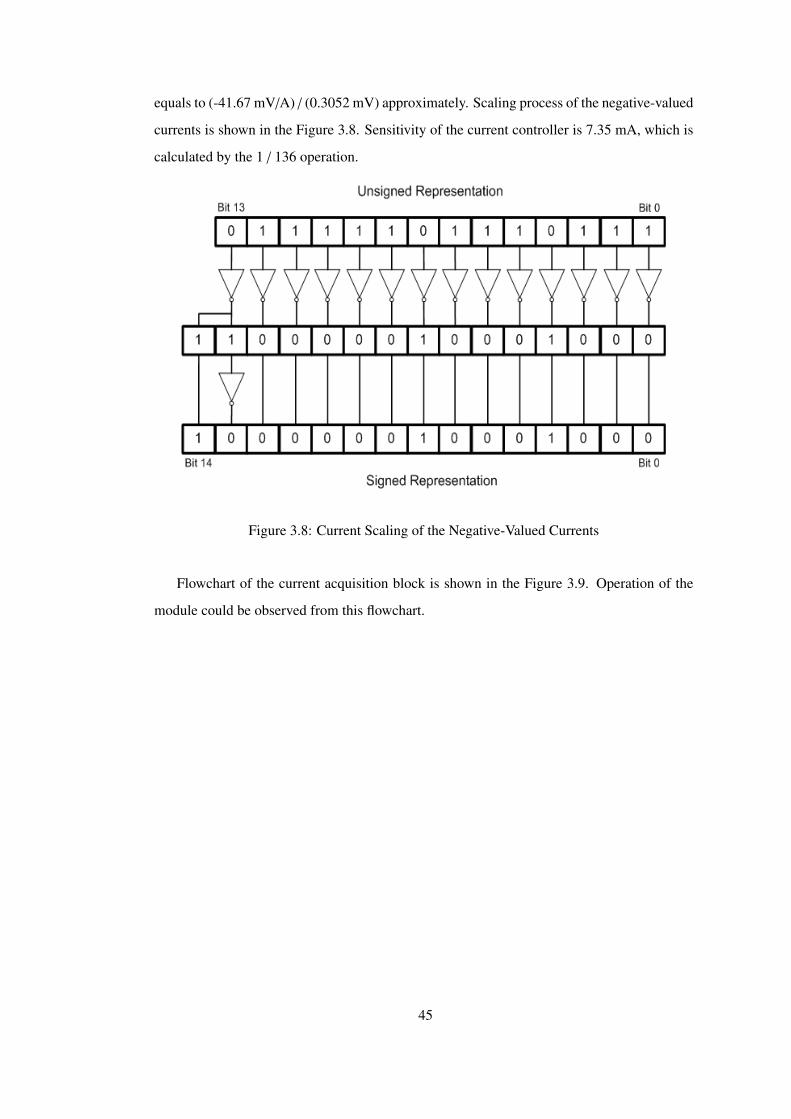
equals to (-41.67 mV/A) / (0.3052 mV) approximately. Scaling process of the negative-valued
currents is shown in the Figure 3.8. Sensitivity of the current controller is 7.35 mA, which is
calculated by the 1 / 136 operation.
Figure 3.8: Current Scaling of the Negative-Valued Currents
Flowchart of the current acquisition block is shown in the Figure 3.9. Operation of the
module could be observed from this flowchart.
45

Figure 3.9: Flowchart of the current acquisition block
46

3.1.2 Phase Detection
The current controller includes a phase detection module for the detection of the active phase
of the motor. In addition; this module selects the related input of the multiplexers shown in
the Figure 3.1 according to the hallsensor outputs of the motor and the outputs of the offset
detection module. A Moore type state machine is designed and implemented in the module
according to the Table 3.6.
Table 3.6: Inputs and Outputs of the Phase Current Detection State Machine
PAOS PBOS H1 H2 H3 Select1 Select2 Description0 0 1 0 0 0 0 Select Phase A Current0 0 1 1 0 0 0 Select Phase A Current0 0 0 1 0 0 1 Select Phase B Current0 0 0 1 1 0 1 Select Phase B Current0 0 0 0 1 1 0 Select Phase C Current0 0 1 0 1 1 0 Select Phase C Current1 0 X X X 0 0 Select Phase A Current for
Offset0 1 X X X 0 1 Select Phase B Current for
Offset0 0 0 0 0 1 1 Invalid Combination0 0 1 1 1 1 1 Invalid Combination1 1 X X X 1 1 Invalid Combination
Diagram of the state machine is shown in the Figure 3.10. State transitions are done
according to the PAOS, PBOS and motor hall sensor signals (H1, H2, H3). Select1 and Select2
signals are the outputs of the state machine. PAOS (phase A offset) and PBOS (phase B offset)
signals shown in the Table 3.6 are generated by the offset detection module according to the
offset detect command coming from the bus controller. During the offset detection operation,
hall sensors of the motor are ignored and the output signals of the phase detection module are
driven according to the signals coming from the offset detection module. H1, H2, H3 signals
are the other input signals of the module, and they represent the commutation cycle of the
motor. BLDC motor has six different commutation cycles represented by three bits wide hall
sensor outputs. Two phases of the motor are active at each commutation cycle. Current flows
into the motor over one of the phases and flows out over the other phase. The phase current
detection table must be updated before using this controller with a different motor, because
commutation table can vary for another motor model.
47
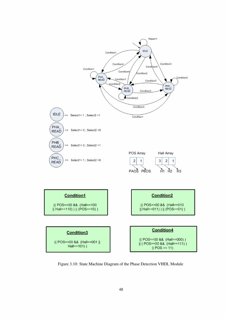
Figure 3.10: State Machine Diagram of the Phase Detection VHDL Module
48

Structure of the phase detection VHDL module is shown in the Figure 3.11. As can be
seen from the Figure; module has a 3 bits wide sensor status port, which shows the status
of the motor’s hall sensors. In order to monitor; this port is used by the bus controller mod-
ule. Connection of the phase detection module with the current integrator and offset detection
modules is shown in the following sections. Input and output ports of the module are ex-
plained in the Table 3.7.
Figure 3.11: Phase detection VHDL module
Table 3.7: Port Decsriptions of the Phase Detection Module
Port Name Width Direction DescriptionCLK−50MHZ 1 bit In Clock Input 50 MHz
RST 1 bit In Module Active High Reset SignalH1 1 bit In First Hall Sensor of the MotorH2 1 bit In Second Hall Sensor of the MotorH3 1 bit In Third Hall Sensor of the Motor
PAOS 1 bit In Select phase A current automaticallyfor the offset detection.
PBOS 1 bit In Select phase B current automaticallyfor the offset detection.
S ensor−S tatus 3 bits Out Holds the status of the motor hall sensorsignals
Select 2 bit Out Shows the active phase of the motor.
49
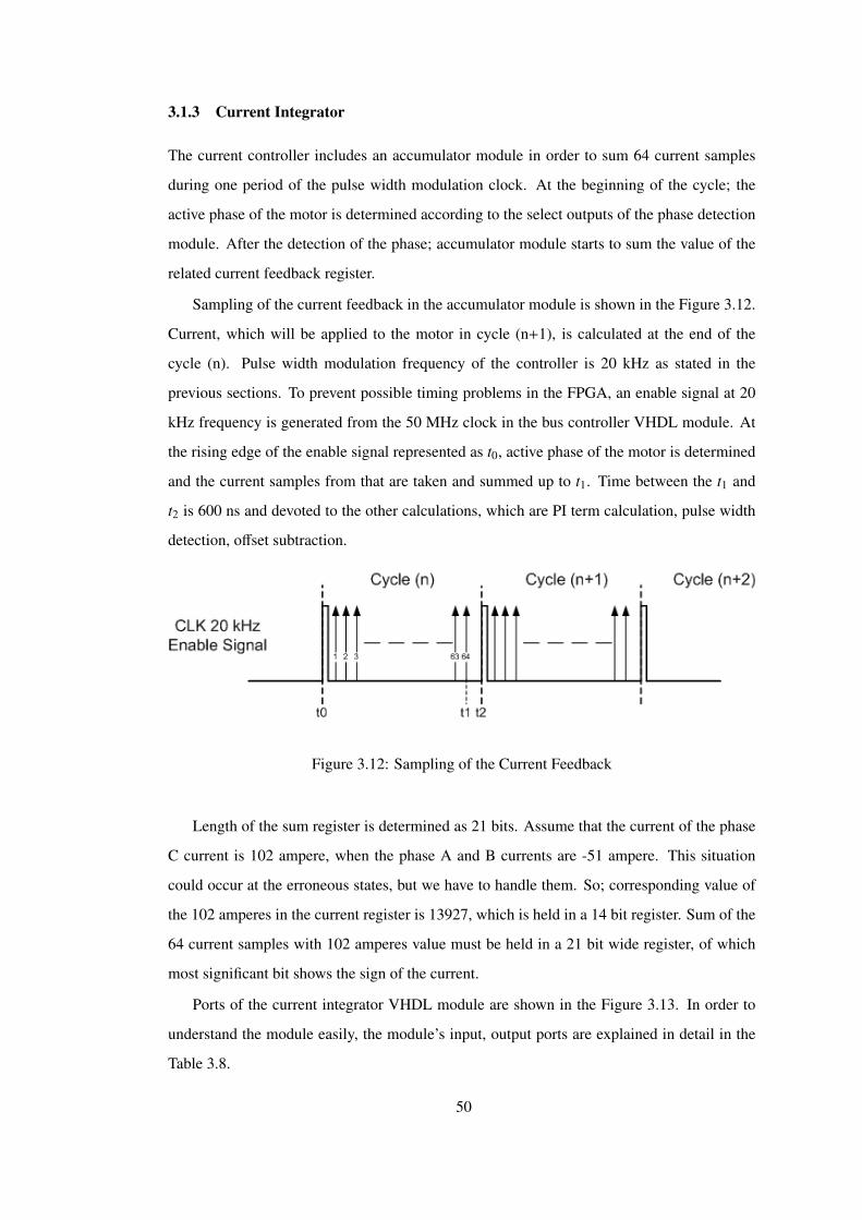
3.1.3 Current Integrator
The current controller includes an accumulator module in order to sum 64 current samples
during one period of the pulse width modulation clock. At the beginning of the cycle; the
active phase of the motor is determined according to the select outputs of the phase detection
module. After the detection of the phase; accumulator module starts to sum the value of the
related current feedback register.
Sampling of the current feedback in the accumulator module is shown in the Figure 3.12.
Current, which will be applied to the motor in cycle (n+1), is calculated at the end of the
cycle (n). Pulse width modulation frequency of the controller is 20 kHz as stated in the
previous sections. To prevent possible timing problems in the FPGA, an enable signal at 20
kHz frequency is generated from the 50 MHz clock in the bus controller VHDL module. At
the rising edge of the enable signal represented as t0, active phase of the motor is determined
and the current samples from that are taken and summed up to t1. Time between the t1 and
t2 is 600 ns and devoted to the other calculations, which are PI term calculation, pulse width
detection, offset subtraction.
Figure 3.12: Sampling of the Current Feedback
Length of the sum register is determined as 21 bits. Assume that the current of the phase
C current is 102 ampere, when the phase A and B currents are -51 ampere. This situation
could occur at the erroneous states, but we have to handle them. So; corresponding value of
the 102 amperes in the current register is 13927, which is held in a 14 bit register. Sum of the
64 current samples with 102 amperes value must be held in a 21 bit wide register, of which
most significant bit shows the sign of the current.
Ports of the current integrator VHDL module are shown in the Figure 3.13. In order to
understand the module easily, the module’s input, output ports are explained in detail in the
Table 3.8.
50
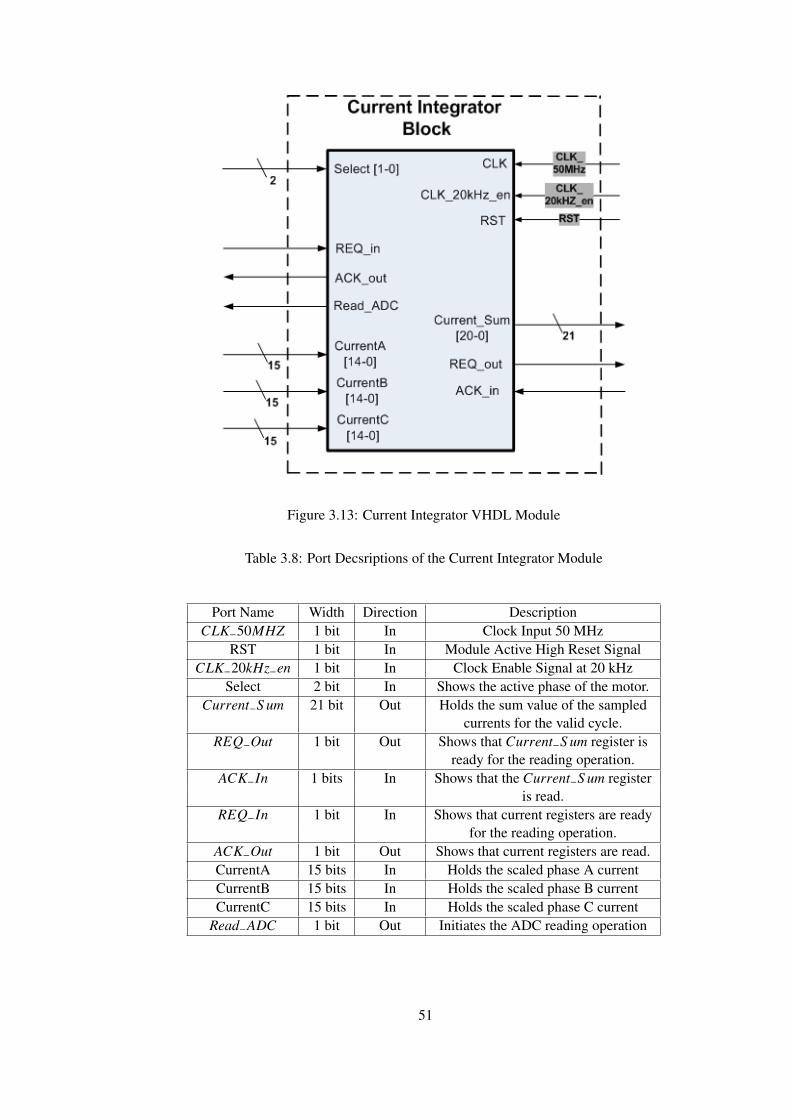
Figure 3.13: Current Integrator VHDL Module
Table 3.8: Port Decsriptions of the Current Integrator Module
Port Name Width Direction DescriptionCLK−50MHZ 1 bit In Clock Input 50 MHz
RST 1 bit In Module Active High Reset SignalCLK−20kHz−en 1 bit In Clock Enable Signal at 20 kHz
Select 2 bit In Shows the active phase of the motor.Current−S um 21 bit Out Holds the sum value of the sampled
currents for the valid cycle.REQ−Out 1 bit Out Shows that Current−S um register is
ready for the reading operation.ACK−In 1 bits In Shows that the Current−S um register
is read.REQ−In 1 bit In Shows that current registers are ready
for the reading operation.ACK−Out 1 bit Out Shows that current registers are read.CurrentA 15 bits In Holds the scaled phase A currentCurrentB 15 bits In Holds the scaled phase B currentCurrentC 15 bits In Holds the scaled phase C current
Read−ADC 1 bit Out Initiates the ADC reading operation
51

Connection between the current integrator module, current acquisition block and phase
detection modules is shown in the Figure 3.14. Current integrator module communicates with
the current acquisition block via handshaking protocol. When the phase current registers are
ready, REQ port of the current acquisition block is set to 1. After that; current integrator block
reads the related current register according to the select output ports of the phase detection
module and set the ACK−out port to 1. In a similar way; current integrator module talks with
the average current calculation module over the REQ−out and ACK−in signals.
52
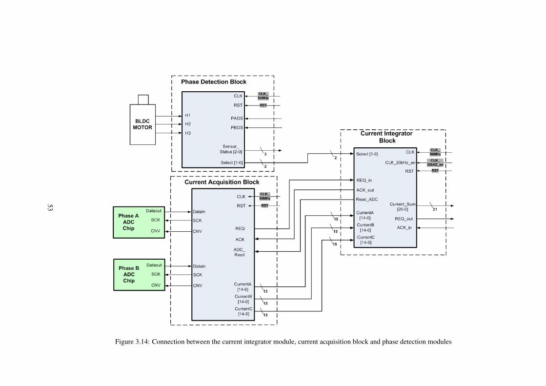
Figure 3.14: Connection between the current integrator module, current acquisition block and phase detection modules
53

Flowchart of the current integrator module is shown in the Figure 3.15. Part shown in the
dashed lines is also available for the phase B and phase C current integrator blocks.
Figure 3.15: Flowchart of the current integrator block
54

Operation of the current integrator module for one cycle is shown in the Figure 3.16. Aim
of this simulation is to verify the summation functionality of the module and to show the
communication with the other modules. In this simulation; active phase of the motor is set
to A and the current of it is determined as 227 mA. However; value of the phase current is
shown as 31 due to scaling operations, which are explained in the previous sections. So; at
the end of sampling, value of the current−sum register will be 1984, which equals to 64*31.
As can be seen from the Figure 3.16, current integrator module drives the REQ−out signal as
1 when the current−sum register is ready. After that; value of the REQ−out signal is set to 0
after catching the ACK−in signal as 1.
Figure 3.16: Simulation of the Current Integrator
3.1.4 Average Current Calculation
In this module; sum register of the current feedback samples is shifted to the right six times
in order to divide by 64. Output of this module is the average current of the active phase in
the recent cycle. Operation of the module is shown in the Figure 3.17 over an example.
The values of the all current samples are assumed as -1 ampere in the example. So; the
value of the current acquisition module’s output current register will be -136 in the signed rep-
resentation. At the end of the operation cycle; value of the current−sum register will be -8704
in the signed representation. After the six shift right operations, value of the average current
register will take -136 value in the average current calculation module. Also; sign bit of the
55

Figure 3.17: Average current calculation
average current register will be at the fourteenth bit location after the shift operations. Length
of the module’s output register is 15 bits because the most significant 6 bits are discarded.
Ports of the average current calculation module are shown in the Figure 3.18.
Figure 3.18: Average Current Calculation VHDL Module
In order to understand the module easily, the module’s input, output ports are explained
in detail in the Table 3.9.
56
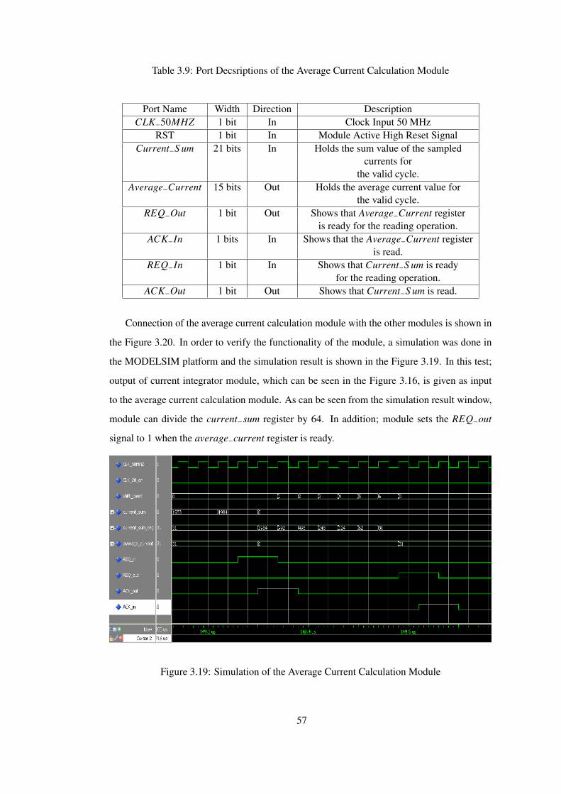
Table 3.9: Port Decsriptions of the Average Current Calculation Module
Port Name Width Direction DescriptionCLK−50MHZ 1 bit In Clock Input 50 MHz
RST 1 bit In Module Active High Reset SignalCurrent−S um 21 bits In Holds the sum value of the sampled
currents forthe valid cycle.
Average−Current 15 bits Out Holds the average current value forthe valid cycle.
REQ−Out 1 bit Out Shows that Average−Current registeris ready for the reading operation.
ACK−In 1 bits In Shows that the Average−Current registeris read.
REQ−In 1 bit In Shows that Current−S um is readyfor the reading operation.
ACK−Out 1 bit Out Shows that Current−S um is read.
Connection of the average current calculation module with the other modules is shown in
the Figure 3.20. In order to verify the functionality of the module, a simulation was done in
the MODELSIM platform and the simulation result is shown in the Figure 3.19. In this test;
output of current integrator module, which can be seen in the Figure 3.16, is given as input
to the average current calculation module. As can be seen from the simulation result window,
module can divide the current−sum register by 64. In addition; module sets the REQ−out
signal to 1 when the average−current register is ready.
Figure 3.19: Simulation of the Average Current Calculation Module
57

Figure 3.20: Connection of the average current calculation module with the other modules
58
3.1.5 Offset Current Detection
The current controller module includes an offset detection module for minimizing the error
term of the current sensor’s output voltage. Output voltage of the current sensor is calculated
according to the Equation 3.4. Error term of the equation depends on many parameters such
as magnitude of the current, ambient temperature, electrical offset voltage, sensitivity and
linearity errors of the sensor. In addition; ADC chips and filter circuits at the input of them
can result in offset error on the current feedback. Offset detection module samples the average
feedback current of the motor for 1.2 second before the activation command coming from the
processor. When the processor sends the activate command to the controller, the detection
module stops the sampling and provides the offset value of the previous cycle. This process
must be done before the activation of the motors because we know that zero ampere is flowing
through the motors.
Offset detection module firstly drives the PAOS (phase A offset) and PBOS (phase B
offset) signals to select the phase A of the motor. Selection process is provided in the Table
3.6. After that; module samples and add the average current of the phase A during 512 mili
seconds. The same process is done for the phase B of the motor. Accumulation part of the
offset detection module is similar to the current integrator module’s design. At the end of
1.2 second; offset current values of A and B phases are calculated by the division operation.
Division operation is done by shifting the current sum registers 11 times. Offset current
of phase C is calculated according to equation 3.2. This process is repeated up to motor
activation command coming from the processor. Module samples the output of the average
current calculation module 2048 times at 250 us period for one phase. So; sampling time of
one phase will be 512 ms. Length of the current sum registers in the module is determined
as 26 bits because maximum value of the sum registers can be 67106816, which equals to
2048*32767. So; 26 bits length sum registers can hold the maximum value. Flowchart of the
offset current detection VHDL module is shown in the Figure 3.21.
After the motor activation command; offset detection module stops to sample and provides
the offset current of each phase to the multiplexer, which is also shown in the Figure 3.1. In
the normal operation mode; input selection of the multiplexer is done according to the select
outputs of the phase detection module. After that; related offset value is subtracted from the
average current feedback.
59
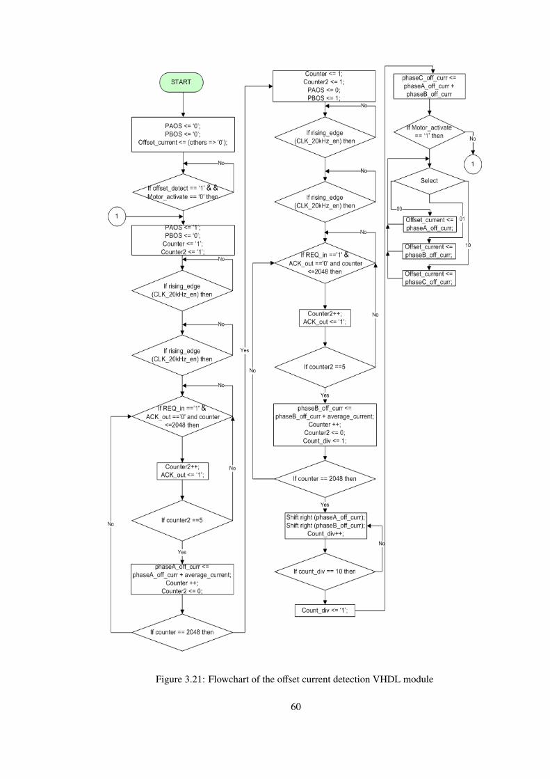
Figure 3.21: Flowchart of the offset current detection VHDL module
60

Offset detection module reduces the effect of the error term in the Equation 3.4 dramat-
ically. The effects of the ambient temperature and electrical offset voltage are removed by
this process. However; sensitivity and linearity errors of the sensor cannot be removed by
this module. To remove the effects of these errors, different techniques such as look-up ta-
ble must be implemented in the FPGA, but implementation of these techniques increases the
complexity of the design at a serious level in terms of utilization of sources and routing of the
clock.
Ports of the offset detection VHDL module are shown in the Figure 3.22. In order to
understand the module easily, the module’s input, output ports are explained in detail in the
Table 3.10. Offset detect and motor activation commands come from the processor and the
module begins to sample average phase current by the offset detect command.
Figure 3.22: Offset Detection VHDL Module
Connection diagram in the Figure 3.20 is updated by adding the offset detection module
and its connections. New connection diagram is shown in the Figure 3.23.
In order to show the operation of the module, several simulations were done in the MOD-
ELSIM platform and one of the simulation results is shown in the Figure 3.24. As can be seen
from the simulation result; sampling period of the phase A is 512 ms and the total period is
1024 ms. Value of the phase A and B offset currents were assumed as 28 mA corresponding
61
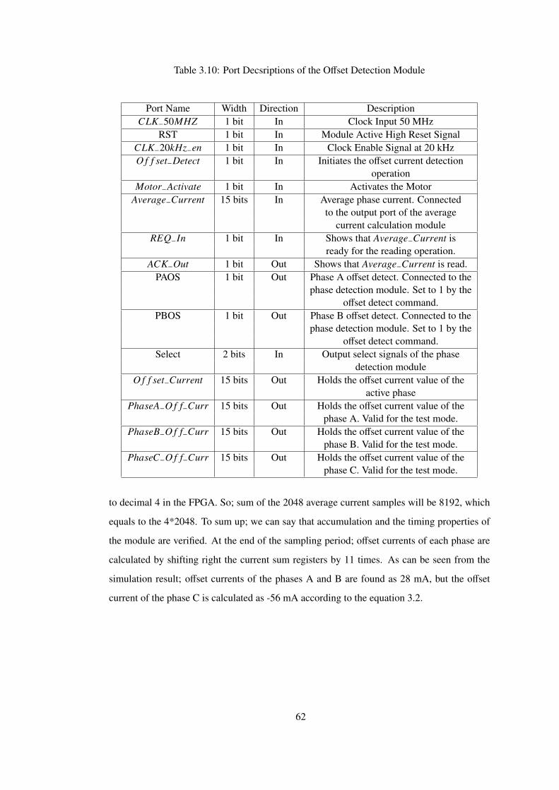
Table 3.10: Port Decsriptions of the Offset Detection Module
Port Name Width Direction DescriptionCLK−50MHZ 1 bit In Clock Input 50 MHz
RST 1 bit In Module Active High Reset SignalCLK−20kHz−en 1 bit In Clock Enable Signal at 20 kHzO f f set−Detect 1 bit In Initiates the offset current detection
operationMotor−Activate 1 bit In Activates the Motor
Average−Current 15 bits In Average phase current. Connectedto the output port of the average
current calculation moduleREQ−In 1 bit In Shows that Average−Current is
ready for the reading operation.ACK−Out 1 bit Out Shows that Average−Current is read.
PAOS 1 bit Out Phase A offset detect. Connected to thephase detection module. Set to 1 by the
offset detect command.PBOS 1 bit Out Phase B offset detect. Connected to the
phase detection module. Set to 1 by theoffset detect command.
Select 2 bits In Output select signals of the phasedetection module
O f f set−Current 15 bits Out Holds the offset current value of theactive phase
PhaseA−O f f−Curr 15 bits Out Holds the offset current value of thephase A. Valid for the test mode.
PhaseB−O f f−Curr 15 bits Out Holds the offset current value of thephase B. Valid for the test mode.
PhaseC−O f f−Curr 15 bits Out Holds the offset current value of thephase C. Valid for the test mode.
to decimal 4 in the FPGA. So; sum of the 2048 average current samples will be 8192, which
equals to the 4*2048. To sum up; we can say that accumulation and the timing properties of
the module are verified. At the end of the sampling period; offset currents of each phase are
calculated by shifting right the current sum registers by 11 times. As can be seen from the
simulation result; offset currents of the phases A and B are found as 28 mA, but the offset
current of the phase C is calculated as -56 mA according to the equation 3.2.
62

Figure 3.23: Connection of the offset detection block with the other modules
63

Figure 3.24: Simulation of the Offset Detection Module
64

3.1.6 Offset Current Subtraction
Current controller module includes a offset current subtraction module for subtracting the
offset current from the average current. This module corresponds to the summation block,
which is shown in the Figure 3.1. This module takes the inputs from the average current
calculation and offset detection modules. In addition; it communicates with these modules
by the handshaking protocol. This module is activated by the motor activate command and it
begins to calculate feedback current with the activation command.
Ports of the offset current subtraction module are shown in the Figure 3.25. Port descrip-
tion table is not provided in this part because it is similar to the previous ones. When the new
feedback current is calculated, curr−RDY signal is set to 1. In order to catch the value of the
f eedback−current register, this signal is used by the bus controller module.
Figure 3.25: Offset current subtraction VHDL module
Figure 3.26 shows the flowchart of the offset current subtraction VHDL module. Opera-
tion of the module can be seen from this flowchart.
By adding the offset current subtraction module to the connection diagram shown in the
Figure 3.23, feedback current reading block will be formed. So; the structure of the feedback
current reading block is shown in the Figure 3.27.
65

Figure 3.26: Flowchart of the offset current subtraction VHDL module
66

Figure 3.27: Feedback Current Reading Block
67
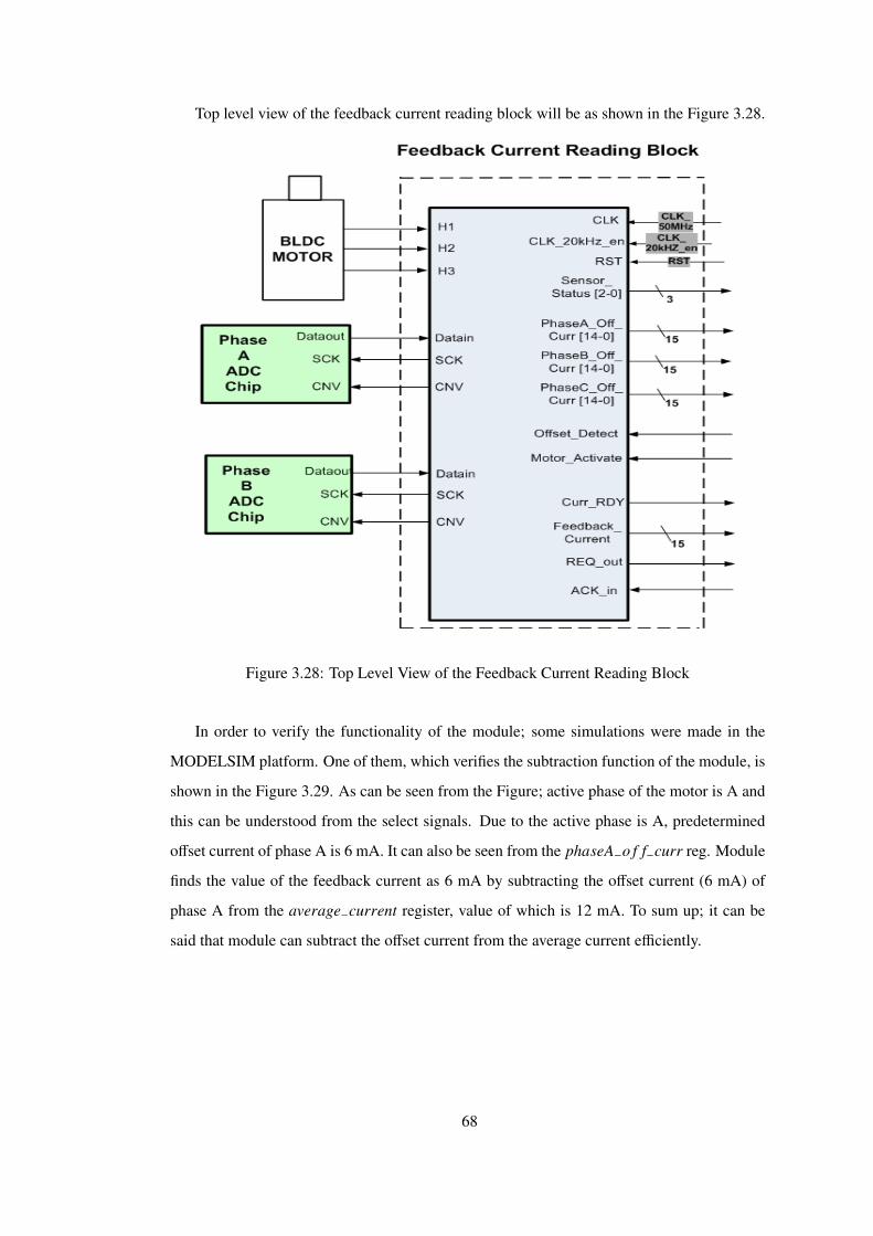
Top level view of the feedback current reading block will be as shown in the Figure 3.28.
Figure 3.28: Top Level View of the Feedback Current Reading Block
In order to verify the functionality of the module; some simulations were made in the
MODELSIM platform. One of them, which verifies the subtraction function of the module, is
shown in the Figure 3.29. As can be seen from the Figure; active phase of the motor is A and
this can be understood from the select signals. Due to the active phase is A, predetermined
offset current of phase A is 6 mA. It can also be seen from the phaseA−o f f−curr reg. Module
finds the value of the feedback current as 6 mA by subtracting the offset current (6 mA) of
phase A from the average−current register, value of which is 12 mA. To sum up; it can be
said that module can subtract the offset current from the average current efficiently.
68

Figure 3.29: Simulation Result Window of the Offset Current Subtraction Module
3.1.7 Error Current Calculation
Current controller includes an error current calculation VHDL module. This module subtracts
the feedback current from the current command in a few cycles and it provides the current
error value to the PI controller module. Bus controller module updates the current command
register of the error current calculation module according to the commands coming from the
processor. However; feedback current information is taken from the feedback current reading
block according to the status of the REQ−out port of that module. When the REQ−out port
of the feedback current reading block is set to 1, error current calculation module latches
the f eedback−current register of the feedback current reading module. After that; feedback
current register is compared with the current limit value, which is determined by the user. As
stated in the Table 3.1, current limit is set to 25 ampere for our setup. If the feedback current
register value is higher than the current limit value, high−current status signal is set to 1. After
this control; error current is calculated by subtracting the feedback current register value from
the current command register value. When the calculation of the error current register value
is completed, a request signal is generated for showing the ready of the register. In addition to
these; this module has a 3 bits wide port called as test−mode, which determines the operation
69
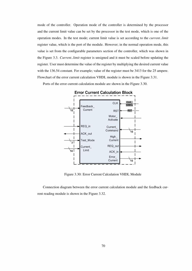
mode of the controller. Operation mode of the controller is determined by the processor
and the current limit value can be set by the processor in the test mode, which is one of the
operation modes. In the test mode; current limit value is set according to the current−limit
register value, which is the port of the module. However; in the normal operation mode, this
value is set from the configurable parameters section of the controller, which was shown in
the Figure 3.3. Current−limit register is unsigned and it must be scaled before updating the
register. User must determine the value of the register by multiplying the desired current value
with the 136.54 constant. For example; value of the register must be 3413 for the 25 ampere.
Flowchart of the error current calculation VHDL module is shown in the Figure 3.31.
Ports of the error current calculation module are shown in the Figure 3.30.
Figure 3.30: Error Current Calculation VHDL Module
Connection diagram between the error current calculation module and the feedback cur-
rent reading module is shown in the Figure 3.32.
70

Figure 3.31: Flowchart of the error current calculation VHDL module
71
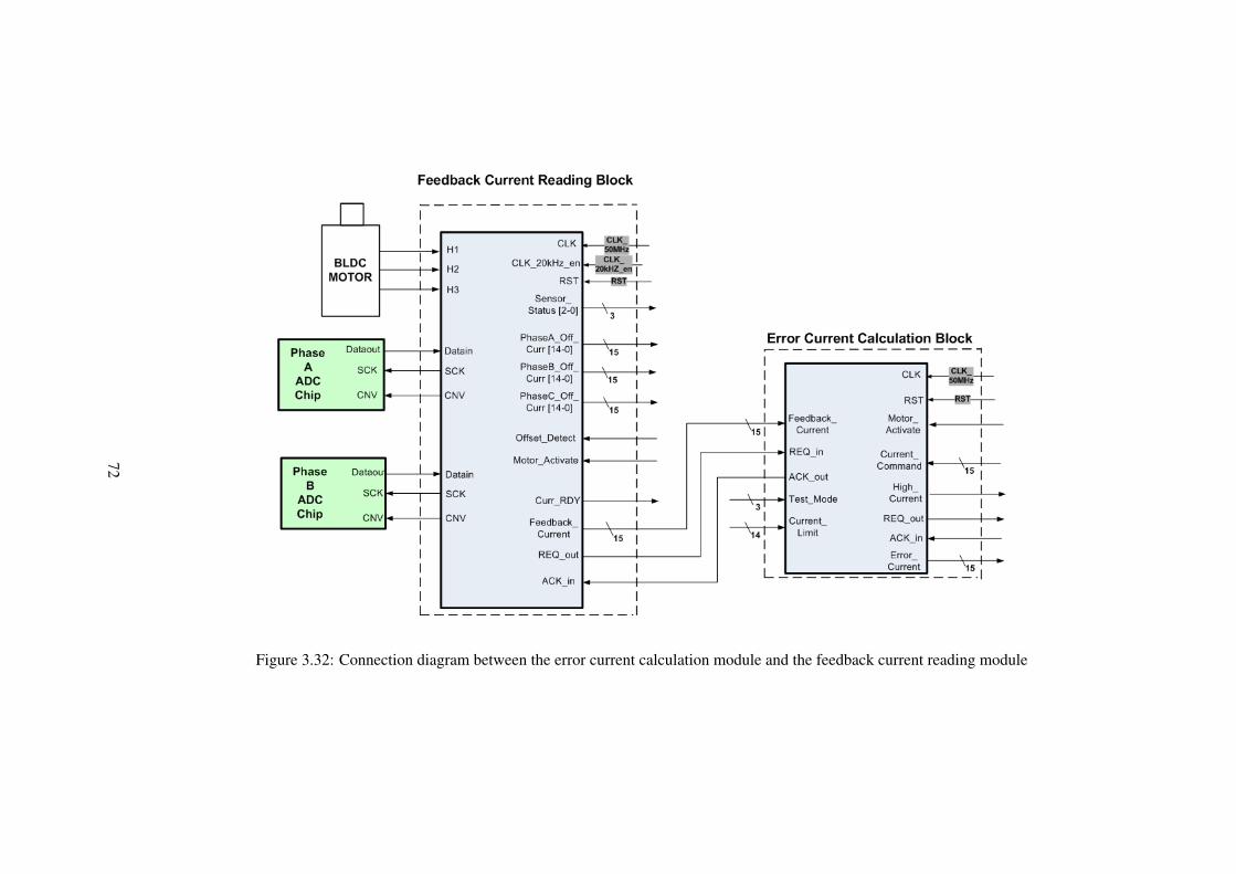
Figure 3.32: Connection diagram between the error current calculation module and the feedback current reading module
72

In order to verify the functionality of the module; some simulations were made in the
MODELSIM platform. One of them, which is done for verifying the subtraction and the
comparison functions of the module, is shown in the Figure 3.33. As can be seen from the
Figure; REQ−in signal is set to 1 and the value of the f eedback−current register is changed
from 0x0000 (0 A) to 0x40CB (-1.48 A) at 748.7 us by the feedback current reading module.
At that time; value of the current−command register is 0x02FF corresponding to the +5.61
ampere. The fourteenth bit of these registers shows the sign of the current. After two clock
cycles; error current is calculated as 0x3C7 (+7.1 A), which equals to the subtraction differ-
ence of the current command and the feedback current. In addition; high current status signal
is set to 1 at the same time because the feedback current value is higher than the current limit,
which is set to 1 ampere. When the register error−current is ready, REQ−out signal is driven
as 1 until the value of ACK−in signal is 1.
73

Figure 3.33: Simulation Result Window of the Error Current Calculation Module
74

3.1.8 PI Controller
We decided to use a proportional-integral controller in the current controller module based
on the implementation difficulty and the simulations in the MATLAB platform. Also; PI
controller is the most commonly used feedback controller in the current control loops [1], [3],
[4], [5]. A general expression of the PI controller in the continuous domain is shown in the
Equation 3.5. In order to implement in the FPGA, this expression must be converted to the
discrete domain.
PI(t) = Ki
∫ t
0e(t) dt + Kpe(t) (3.5)
Ki : Integral gain, a tuning parameter
Kp :Proportional gain, a tuning parameter
e(t) : Error
t : Time or instantaneous time (the present)
In order to discretize the integral term, we focused on two methods, trapezoidal and rect-
angule. The trapezoidal rule is a numerical method that approximates the value of a definite
integral. For a domain discretized into N subintervals using N+1 points, where the length of
subintervals is h = (t-0) / N, the approximation to the integral term becomes
∫ t
0e(t) dt ≈
h2
N∑k=1
(e(xk) + e(xk−1)) (3.6)
Another approximation technique for the discretization of integral term is rectangule rule. For
a domain discretized into N subintervals using N+1 points, where the length of subintervals
is h = (t-0) / N, the approximation to the integral term becomes
∫ t
0e(t) dt ≈ h
N∑k=1
e(xk) (3.7)
We decided to use rectangle rule compared with the trapezoidal rule in terms of implementa-
tion difficulties. However; equation of the trapezoidal rule gives more exact results compared
75
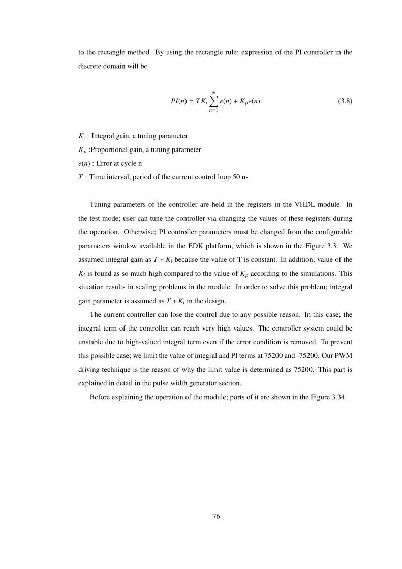
to the rectangle method. By using the rectangle rule; expression of the PI controller in the
discrete domain will be
PI(n) = T Ki
N∑n=1
e(n) + Kpe(n) (3.8)
Ki : Integral gain, a tuning parameter
Kp :Proportional gain, a tuning parameter
e(n) : Error at cycle n
T : Time interval, period of the current control loop 50 us
Tuning parameters of the controller are held in the registers in the VHDL module. In
the test mode; user can tune the controller via changing the values of these registers during
the operation. Otherwise; PI controller parameters must be changed from the configurable
parameters window available in the EDK platform, which is shown in the Figure 3.3. We
assumed integral gain as T ∗ Ki because the value of T is constant. In addition; value of the
Ki is found as so much high compared to the value of Kp according to the simulations. This
situation results in scaling problems in the module. In order to solve this problem; integral
gain parameter is assumed as T ∗ Ki in the design.
The current controller can lose the control due to any possible reason. In this case; the
integral term of the controller can reach very high values. The controller system could be
unstable due to high-valued integral term even if the error condition is removed. To prevent
this possible case; we limit the value of integral and PI terms at 75200 and -75200. Our PWM
driving technique is the reason of why the limit value is determined as 75200. This part is
explained in detail in the pulse width generator section.
Before explaining the operation of the module; ports of it are shown in the Figure 3.34.
76

Figure 3.34: PI controller VHDL module
As stated in the previous parts; pi controller parameters can be set by the user during the
operation. When the processor sets the mode of the controller as test mode, user can set the
controller parameters by updating the values of the PI−K p−Test and PI−T KI−Test registers.
After the configuration of the module is completed; module will be ready for the operation.
A state machine is designed and implemented in the PI controller in order to control the flow.
Diagram of the state machine is shown in the Figure 3.35.
77
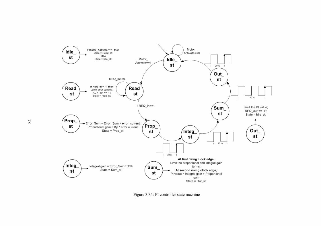
Figure 3.35: PI controller state machine
78

At the beginning of the operation; module waits the motor activation command. When the
activation command is set to 1, state changes to read state. In this state; PI controller module
latches the error current register of the error current calculation module when the REQ−out
port of that module is set to 1. At the same time; state changes to proportional state. In this
state; error sum term is updated according to the new error current value and the propotional
gain is calculated. These operations are completed in one clock cycle and state is changed
to the integral state at the rising edge of the clock. In the integral state; the integral gain is
calculated in one cycle by multiplying the error sum term with the TKi parameter. In the next
cycle; state will be sum state and the proportional and the integral terms are compared with
the limit values 75200 and -75200. At the second rising clock edge; PI term is calculated by
adding the integral and proportional terms and state is changed to the out state. In the out
state; PI term is limited at the values 75200 and -75200 and REQ−out signal is driven as 1. In
the next cycle; state returns to idle and activation command is checked again.
In order to verify the functionality of the module; some simulations were made in the
MODELSIM platform. One of them, which is done for verifying the state machine diagram
and the operations of the module, is shown in the Figure 3.36. As can be seen from the
Figure; value of the error current register is 667 corresponding to 4.89 ampere and Kp and
TKI parameters of the controller are set to 50 and 6 respectively. In addition; saturation
limit of the controller is set to 75200, which can be seen from the PI−S at−Limit register. If
we analyze the simulation result, we see that state transitions are done correctly in terms of
timing. In the prop−st; error sum register is updated and the new value of it is 1334. In
addition; proportional gain term is calculated as 33350, which equals to 50*667. After that;
state is changed to integ−st and integral gain term is calculated as 8004, which equals to the
6*1334. At the end of the sum state; PI value is calculated as 41354, which equals to the
8004+33350. Finally; PI value is compared with the saturation limit value and REQ−out
signal is set to 1 in the state out−st.
Connection of the PI controller module with the other modules is shown in the Figue 3.37.
79

Figure 3.36: Simulation Result Window of the PI Controller Module
80

Figure 3.37: Connection of the PI controller module with the other modules
81

3.1.9 Pulse Width Generator
In the analog circuit based motor drivers; resolution of the pulse width is infinity. However;
pulse width resolution has to be defined for the digital implementations. We determined the
pulse width resolution as %0.04 (1/2500) , the highest resolution that can be achieved by the
system. Because the maximum clock frequency in the system is 50 MHz, one PWM period
(50 us) can be divided into 2500 slices. So; controller generates a pulse width modulation
signal at 20kHz frequency with minimum %0.04 duty cycle. In this module; the value of
the PI term is mapped between 75 and 2425 corresponding to %3 and %97 pulse widths
respectively. This module does not allow to %0 and %100 pulse widths because of bootstrap
type mosfet drivers. A time period of 1.5 us corresponding to %3 pulse width is devoted to
the charging of capacitors. Mapping of the PI term to the pulse width is shown in the Figure
3.38.
Figure 3.38: PI versus Pulse Width
To convert the output of the PI controller to the pulse width; the formula, which is pro-
vided in the Equation 3.9, is implemented in this module. The division operation is done by
shifting the register to the right six times.
82

PW(n) = 1250 +PI(n)
64(3.9)
PW(n) : Pulse wdth at cycle n
PI(n) : PI value at cycle n
Ports of the module are shown in the Figure 3.39.
Figure 3.39: Pulse width generator module
Module communicates with the PI controller and commutation control modules. Mod-
ule latches the output port of the PI controller module, which is called PI−term, when the
REQ−out output port of the same is set to 1. Module begins to operate with the arrival of the
new data and the PI term register is shifted to the right six times. By this way; PI term register
is divided to 64. After the division operation; updated register is summed with the 1250 value.
Finally; the pulse width becomes the value of the final value of the register. When the pulse
width calculation is completed, REQ−out signal is driven as 1. Flowchart of the pulse width
generator module is shown in the Figure 3.40.
83
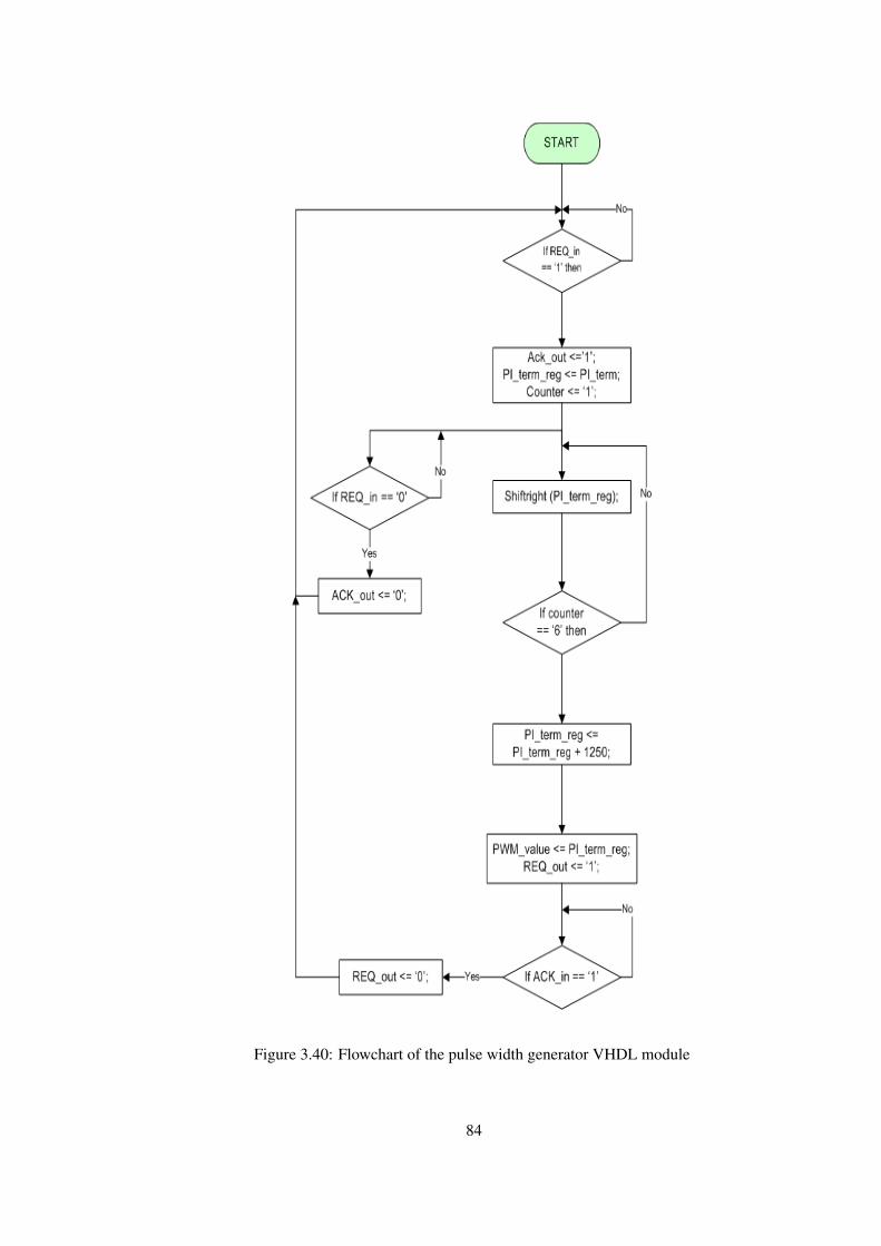
Figure 3.40: Flowchart of the pulse width generator VHDL module
84
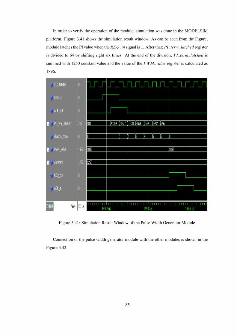
In order to verify the operation of the module, simulation was done in the MODELSIM
platform. Figure 3.41 shows the simulation result window. As can be seen from the Figure;
module latches the PI value when the REQ−in signal is 1. After that; PI−term−latched register
is divided to 64 by shifting right six times. At the end of the division; PI−term−latched is
summed with 1250 constant value and the value of the PWM−value register is calculated as
1896.
Figure 3.41: Simulation Result Window of the Pulse Width Generator Module
Connection of the pulse width generator module with the other modules is shown in the
Figure 3.42.
85

Figure 3.42: Connection between the pulse width generator module and the other VHDL modules
86
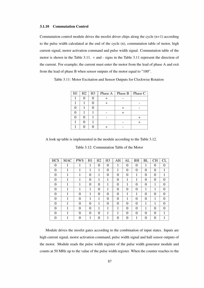
3.1.10 Commutation Control
Commutation control module drives the mosfet driver chips along the cycle (n+1) according
to the pulse width calculated at the end of the cycle (n), commutation table of motor, high
current signal, motor activation command and pulse width signal. Commutation table of the
motor is shown in the Table 3.11. + and - signs in the Table 3.11 represent the direction of
the current. For example; the current must enter the motor from the lead of phase A and exit
from the lead of phase B when sensor outputs of the motor equal to ”100”.
Table 3.11: Motor Excitation and Sensor Outputs for Clockwise Rotation
H1 H2 H3 Phase A Phase B Phase C1 0 0 + -1 1 0 + -0 1 0 + -0 1 1 - +
0 0 1 - +
1 0 1 - +
1 0 0 + -
A look up table is implemented in the module according to the Table 3.12.
Table 3.12: Commutation Table of the Motor
HCS MAC PWS H1 H2 H3 AH AL BH BL CH CL0 1 1 1 0 0 1 0 0 1 0 00 1 1 1 1 0 1 0 0 0 0 10 1 1 0 1 0 0 0 1 0 0 10 1 1 0 1 1 0 1 1 0 0 00 1 1 0 0 1 0 1 0 0 1 00 1 1 1 0 1 0 0 0 1 1 00 1 0 1 0 0 0 1 1 0 0 00 1 0 1 1 0 0 1 0 0 1 00 1 0 0 1 0 0 0 0 1 1 00 1 0 0 1 1 1 0 0 1 0 00 1 0 0 0 1 1 0 0 0 0 10 1 0 1 0 1 0 0 1 0 0 1
Module drives the mosfet gates according to the combination of input states. Inputs are
high current signal, motor activation command, pulse width signal and hall sensor outputs of
the motor. Module reads the pulse width register of the pulse width generator module and
counts at 50 MHz up to the value of the pulse width register. When the counter reaches to the
87

register value, pulse width signal falls from one to zero. The pulse width signal, high current
signal and motor activation command are represented as PWS, HCS and MAC respectively
in the Table 3.12.
Because of some erroneous conditions, motors can draw current at high levels like 50, 60
amperes. In this case; power supply or electronic board can be damaged because of high-level
current. To prevent this possible damages; high current detection operation is implemented in
the error current calculation module. Error current calculation module compares the feedback
current of the motor with the predefined current limit. If the feedback current is higher than
the current limit, module sets the high current signal to 1. Output signals of the commutation
controller module, AH, AL, BH, BL, CH, CL, represents the mosfets in the inverter circuit.
These signal names are shown on the inverter circuit in the Figure 3.43.
Figure 3.43: Notation of the Commutation Control’s Outputs on the Inverter Circuit
Ports of the commutation control module are shown in the Figure 3.44. Module latches
the pulse width output port of the pulse width generator module when the REQ−in signal is
1. After that clock enable signal named CLK−20kHz−en is sampled and hall sensor signals,
activation command and high current signal are latched at the rising edge of the 20 kHZ enable
signal. According to the look-up table in the Table 3.12. Module begins to drive the mosfet
gate signals with the rising edge of the 20 kHz clock enable signal.
88

Figure 3.44: Commutation Control VHDL Module
In order to show the operation of the module, a simulation result window is shown in the
Figure 3.45. As can be seen from the Figure; latched PWM value is 1958, which corresponds
to the %78.32 pulse width. So; module drives the mosfet gate signals for 39.16 us in a period
of 50 us. Pulse−width−signal in the Figure represents the PWS signal in the Table 3.12.
Figure 3.45: Simulation Result Window of the Commutation Control VHDL Module
Connection of the commutation control module with the other VHDL modules completes
the current controller module structure. So; current controller VHDL module structure is
shown in the Figure 3.46.
89

Figure 3.46: Current Controller VHDL Module Structure
90

Top level view of the current controller module is shown in the Figure 3.47. Ports of the
current controller module were explained in the Table 3.2 and Table 3.3.
Figure 3.47: Top Level View of the Current Controller VHDL Module
91
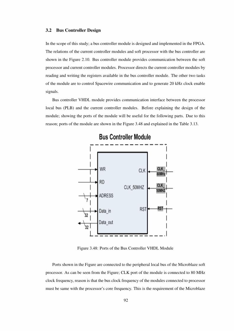
3.2 Bus Controller Design
In the scope of this study; a bus controller module is designed and implemented in the FPGA.
The relations of the current controller modules and soft processor with the bus controller are
shown in the Figure 2.10. Bus controller module provides communication between the soft
processor and current controller modules. Processor directs the current controller modules by
reading and writing the registers available in the bus controller module. The other two tasks
of the module are to control Spacewire communication and to generate 20 kHz clock enable
signals.
Bus controller VHDL module provides communication interface between the processor
local bus (PLB) and the current controller modules. Before explaining the design of the
module; showing the ports of the module will be useful for the following parts. Due to this
reason; ports of the module are shown in the Figure 3.48 and explained in the Table 3.13.
Figure 3.48: Ports of the Bus Controller VHDL Module
Ports shown in the Figure are connected to the peripheral local bus of the Microblaze soft
processor. As can be seen from the Figure; CLK port of the module is connected to 80 MHz
clock frequency, reason is that the bus clock frequency of the modules connected to processor
must be same with the processor’s core frequency. This is the requirement of the Microblaze
92

Table 3.13: Port Decsriptions of the Bus Controller VHDL Module
Port Name Width Direction DescriptionCLK 1 bit In Clock Input. It equals to the clock frequency
of the processor bus.RST 1 bit In Module Active High Reset Signal
CLK−50MHz 1 bit In 50 MHz clock signal for the current controllermodules.
WR 1 bit In Active high write signal.RD 1 bit In Active high read signal
ADRES S 7 bits In Adress signals used for addressing theregisters in the module
Data−in 32 bit In 32 bits wide data input busData−out 32 bit Out 32 bits wide data output bus
soft processor core structure. The other clock port of the module is CLK−50MHz, which is
connected to the 50 MHz clock signal due to the operating clock frequency of the current
controller modules. In the top level, a clock generator module is connected to the processor
core and this module generates 80 MHz clock signal for the processor core and the other
modules. In addition; this module also generates a 50 MHz clock frequency for the current
controller modules. Other ports of the module are used for the data exchange between the
processor and the module.
As stated at the beginning of the section; bus controller module generates 20 kHz enable
signals for the four current controller modules. Actually; module generates four clock enable
signals and there exists 90 degree phase shift between them. Aim of applying phase shift is
to reduce the power consumption on the board. Otherwise; four motors begin to run at the
same time and high level currents can be drawn from the power supply. Timing diagram of
the 20 kHz clock enable signals is shown in the Figure 3.49. As can be seen from the Figure;
pulse width of the enable signals is 10 ns instead of 25 us to prevent the routing of the extra
clock signals in the FPGA. As the number of the clock signals increases in the VHDL design,
routing and the synthesis of the design become diffucult.
Another task of the bus controller module is to provide communication between the pro-
cessor and the current controller VHDL modules.
A list of the registers between the bus controller and soft processor are provided in the
Table 3.14. A section in the address map of the processor is assigned for the current controller
module. Registers of the current controller module are mapped to the related address section
according to the offset address values, which are defined previously by the designer.
93

Figure 3.49: Timing diagram of the 20 kHz clock enable signals
Table 3.14: Registers of the Bus Controller Module
Offset Address Register NameValue (Hex)
0x00 PLB−Test0x04 Control−reg0x08 S tatus−reg0x0C Current−Comm−M1−M20x10 Current−Comm−M3−M40x14 PI−Para0x18 High−Curr−Lim−M1−M20x1C High−Curr−Lim−M3−M40x20 Position−Feed−M10x24 Position−Feed−M20x28 Position−Feed−M30x2C Position−Feed−M40x30 O f f set−Curr−M1−PhaseAB0x34 O f f set−Curr−M1−PhaseC−M2−PhaseA0x38 O f f set−Curr−M2−PhaseBC0x3C O f f set−Curr−M3−PhaseAB0x40 O f f set−Curr−M3−PhaseC−M4−PhaseA0x44 O f f set−Curr−M4−PhaseBC0x48 Position−Comm−M10x4C Position−Comm−M20x50 Position−Comm−M30x54 Position−Comm−M4
PLB Test Register: PLB−Test register is used for testing the peripheral local bus between
the processor and VHDL module. Register is 32 bits wide, readable and writable by the
processor.
Control Register: Control register is used for setting the operation mode of the controller,
94

disabling the fin locks, activating the offset current read operations and enabling the motors.
Register is 32 bits wide, readable and writable by the processor. The bits of the register are
shown in the Figure 3.50.
Bits between 0 and 3 : Motor activation command bits
Bits between 8 and 11 : Offset current read command bits
Bits between 16 and 19 : Fin lock disable command bits
Bits between 24 and 26 : Set the operation mode (Normal and Test modes) of the controller
Figure 3.50: Control Register of the Current Controller Module
Implementation of the control register is shown in the Figure 3.51. As can be seen from
the Figure; input and output busses are connected to the control register via three-state buffers
and enable ports of these buffers are connected to the write and read enable signals. Enable
signals are generated by using the address, read and write signals, which are coming from the
processor bus. Address of the control register is determined as 0x04 and it is also given in the
Table 3.14. So; third bit of the address bus is connected to the ”and” gate directly. However;
other address bits are connected to the and gate via inverter buffers.
Control register holds the motor activation commands, offset current read command and
the operation mode of the controller. Clock port of the register is connected to the 80 MHz
due to the processor bus frequency. However; current controller VHDL modules’ operating
frequency is 50 MHz. So; related bits of the control register are transferred to the motor
activation, offset detect and test mode ports of the current controller module at 50 MHz con-
tinuously except that the write enable signal of the control register is 1. Transfer of the control
register’s related bits to the current controller modules is shown in the Figure 3.52. As can
be seen from the Figure; control register is mapped to the current controller modules’ related
ports via three-state buffers. Enable ports of the buffers are connected to the logic ”not” of
the write enable signal. Reason of that is to prevent the data transfer from the control register
to the modules when the writing operation of the register is active. Otherwise; faulty data can
be transferred to the modules because states of the flip-flops could be uncertain during the
writing operation.
95

Figure 3.51: Implementation of the Control Register
96

Figure 3.52: Mapping of the control register to the current controller modules’ ports
97

Status Register: Status register of the module is used for reading the activation status of
the motors and high current status bits by the processor. Register is 32 bits wide and only
readable by the processor. Structure of the status register is shown in the Figure 3.53.
Figure 3.53: Status Register of the Current Controller Module
Status register is read by the processor at 80 MHz clock frequency. However; bits of
the register are updated by the current controller module at 50 MHz. Because the type of
the register is read only, read enable signal is generated only in the bus controller module.
Mapping between the current control modules and the register is shown in the Figure 3.54.
As can be seen from the Figure, three state type buffers are used between the current controller
and status register. Enable ports of these buffers are connected to the read enable signal, which
is also shown in the Figure. Read enable signal is latched at 80 MHz clock frequency because
the update frequency of the high current ports is 50 MHz. So: 80 MHz sampling frequency is
sufficient for catching the transitions of the signals. In addition; four least significant bits of
the register are updated by the control register. These bits shows the status of the activation
commands.
98
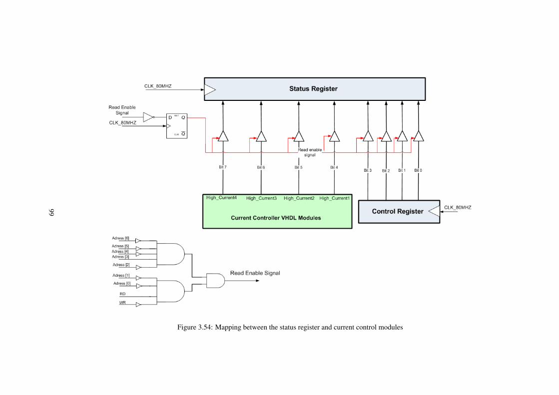
Figure 3.54: Mapping between the status register and current control modules
99

Current Command Registers: These registers are used for holding the current com-
mands of the controllers. Structures of the Current−Comm−M1−M2 and Current−Comm−M3−M4
registers are completely same. 29th and 13th bits of the registers determines the direction of
the current command. Registers are 32 bits wide, readable and writable by the processor.
Structure of the register is shown in the Figure 3.55. Mapping structure of these registers is
similar to the mapping structure of the control register. Read and write enable signals are
generated for these registers and these signals are connected to the enable ports of the three
state buffers, which are used between the current command registers and the current controller
modules.
Figure 3.55: Current Command Register of the Current Controller Module
PI Controller Parameters Register: PI−Para register is used for setting the PI controller
parameters by the processor. Register is 32 bits wide, readable and writable by the processor.
Structure of the register is shown in the Figure 3.56. T Ki and Kp parameters of the controller
are set according to this register value.
Figure 3.56: PI Controller Parameters Register of the Current Controller Module
High Current Limit Registers: High−Curr−Lim−M1−M2 and High−Curr−Lim−M3−M4
registers are completely same. These registers are used for holding the high current limit of
the controllers. The structure of these registers is same with the current command registers’
structure. Registers are 32 bits wide, readable and writable by the processor.
Position Feedback and Position Command Registers: These registers are used for hold-
ing the position of the motors and position commands coming from another board or PC.
These registers are updated by the processor. Values of these registers are sent to the PC
via Spacewire protocol. Registers are 32 bits wide, readable and writable by the processor.
Because there is no communication link between the bus controller module and the encoder
100

reading module, processor writes the output registers of the encoder reading module to these
registers at the beginning of the position control loop.
Offset Current Registers: Offset currents of the motors’ each phase are provided to the
processor with six registers. Structures of all the offset current registers are completely same.
Registers are 32 bits wide and only readable by the processor. Structure of the offset current
register is same with the current command register’s structure.
In the test mode; bus controller module sends the feedback current, pulse width, hall
sensor outputs of the motors, status register, current command, position feedback and position
command to the PC over the Spacewire protocol. A fixed packet structure, whose length is
2111 bytes, is determined for the communication. Structure of the packet is provided in the
Table 3.15.
The module sends this packet at 200 Hz. Module samples the feedback currents, pulse
widths, status register, hall sensor outputs of the motors at 20 kHz and keeps them in a separate
FIFO memory for 5 ms for each motor. The same operation is done for the position command,
position feedback, the current command at 1 kHz sampling frequency because we determined
the operating frequency of the position control loop as 1 kHz. N and m letters in the Table
3.15 represent the position control and current control cycle numbers respectively.
As stated in the previous part; bus controller module holds the feedback data in separate
FIFO memories during 5 ms. At the end of the fifth ms, content of the memories are written
to the Spacewire module. Structure of the feedback data control block is shown in the Figure
3.57. As can be seen from the Figure; four FIFO memories, size of each is 512x9 bits, are
allocated to the four current controller modules. In addition; one FIFO memory at the same
size is used for holding the sensor status data of four motors and the status register of the bus
controller module. Finally; one FIFO memory, whose size is 256x9 bits, is used for holding
the position feedback and position command registers. Writing operation of the memories is
controlled by the FIFO control logic and the reading operation is controlled by the Spacewire
control logic.
101
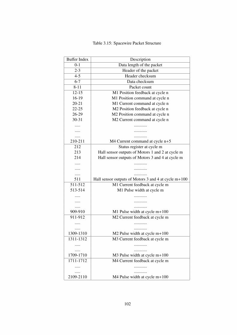
Table 3.15: Spacewire Packet Structure
Buffer Index Description0-1 Data length of the packet2-3 Header of the packet4-5 Header checksum6-7 Data checksum8-11 Packet count
12-15 M1 Position feedback at cycle n16-19 M1 Position command at cycle n20-21 M1 Current command at cycle n22-25 M2 Position feedback at cycle n26-29 M2 Position command at cycle n30-31 M2 Current command at cycle n
..... ............
..... ............
..... ............210-211 M4 Current command at cycle n+5
212 Status register at cycle m213 Hall sensor outputs of Motors 1 and 2 at cycle m214 Hall sensor outputs of Motors 3 and 4 at cycle m..... ................. ................. ............511 Hall sensor outputs of Motors 3 and 4 at cycle m+100
511-512 M1 Current feedback at cycle m513-514 M1 Pulse width at cycle m
..... ............
..... ............
..... ............909-910 M1 Pulse width at cycle m+100911-912 M2 Current feedback at cycle m
..... ............
..... ............1309-1310 M2 Pulse width at cycle m+1001311-1312 M3 Current feedback at cycle m
..... ............
..... ............1709-1710 M3 Pulse width at cycle m+1001711-1712 M4 Current feedback at cycle m
..... ............
..... ............2109-2110 M4 Pulse width at cycle m+100
102

Figure 3.57: Structure of the Feedback Data Control Block
103
3.3 Matlab Simulations
At the beginning of the study; we designed the current controller in the Figure 3.1. How-
ever; there is no way to know whether the suggested controller works efficiently with the
selected brushless motor BLM-25-7. It could be useful to perform some simulations, before
implementing the design. Simulations show the problemeatic parts in the design and give the
chance of fixing these parts before the implementation. In addition; PI controller parameters
can be tuned using the simulations. MATLAB 7.9 Simulink was used for the modeling the
controller design in the Figure 3.1. Motor parameters of the BLM-25-7 are used in the model.
Figure 3.58 shows the MATLAB model of the current controller. Current command is given to
the controller from a signal generator model and 50 us time delay is put on the command line
because current controller’s command update frequency is 20 kHz. Also; current command
and current feedback signals are multiplied by current scale factor, 136.
As can be seen from the model; several time delays, which are current sensor measure-
ment delay (100 ns), ADC chip acquisition and conversion delay (700 ns), error current cal-
culation delay (50 ns), PI calculation delay (120 ns) and pulse width calculation delay (120
ns), are put on the model. By taking these delays into account; model approaches to the real
platform further. In addition to these; motor parameters, which are torque constant (0.128
Nm/A), resistance (0.34 ohm) and inductance (0.33 mH), inertia, viscous damping and back
EMF constant, are reflected to the model.
104

Figure 3.58: MATLAB Model of the Current Controller
105
Saturation Speed Test: The purpose of this simulation is to learn the saturation speed of
the motor for the supply voltage of 28 V. Maximum motor speed is reached when the back
EMF voltage opposes the terminal voltage applied to the motor. In this case; motor does not
draw current from the supply. When the constant current command is applied, the motor will
reach its saturation speed. Output torque equation of the motor is given in the Equation 3.10.
Tm = Kt ∗ Ic (3.10)
Motor shaft equation is,
Tm = Jdwdt
+ Bw + TL (3.11)
Tm : Motor Torque (N − m)
TL : Load Torque (N − m)
w : Motor Speed (rad/sec)
J : Inertia (kg − m2)
B: Viscous Damping ( Nmrad/sec )
Bw term in the Equation 3.11 is negligible because viscous damping coefficient of the
motor is very small. TL term is also negligible because no load is applied to the motor in the
model. So; torque of the motor will be equal to the acceleration term, which is Jdw/dt. When
the motor reaches its saturation speed due to back EMF voltage, motor cannot accelerate and
acceleration term converges to zero. In this case; motor draw negligible current to compensate
TL, and Bw terms.
To observe the saturation speed, torque and back EMF voltage of the motor, 4 A constant
current command is applied to the motor. Motor current will track the 4 A current command
for a short period of time until its saturation speed. After that point; motor draws negligible
current to compensate the viscous damping term in the motor shaft equation. Acceleration
of the motor up to saturation speed is shown in the Figure 3.59. According to the graph;
maximum speed of the motor is 2090 rpm. After the motor reaches its maximum speed;
torque of the motor decreases to a very low value. Motor torque under the constant current
command is shown in the Figure 3.60.
106

Figure 3.59: Motor Speed for the 4 A Current Command
Figure 3.60: Motor Torque for the 4 A Current Command
107

Command Tracking Performance Test: In order to prevent motor from reaching its
maximum speed, a current command, periodic waveform with equal plus and minus portions,
must be applied to the motor. When the motor reaches its saturation speed, the motor draws
negligible current from the supply. In this case; current controller loses the control over the
motor. For this simulation; Kp and Ki parameters are determined as 50 and 120000 respec-
tively. The current command is a square waveform at 50 Hz and peak-to-peak amplitude of
it is 4 A. Current feedback and current command signals are shown in the Figure 3.61. The
red line in the graph represents the current command signal, whereas rectified black signal
current feedback signal. As we can see from the figure; current feedback signal tracks the
command signal effectively.
Figure 3.61: Rectified Current Command and Feedback
Torque of the motor in this test is shown in the Figure 3.62. A graph of the motor torque
can be verified by the Equation 3.12. Torque constant of the motor BLM-25-7 is 0.128 Nm/A.
Tm = Kt ∗ I (3.12)
Tm : Motor Torque (Nm)
Kt : Torque Constant of the Motor ( Nm/A)
I : Motor Current (A)
108
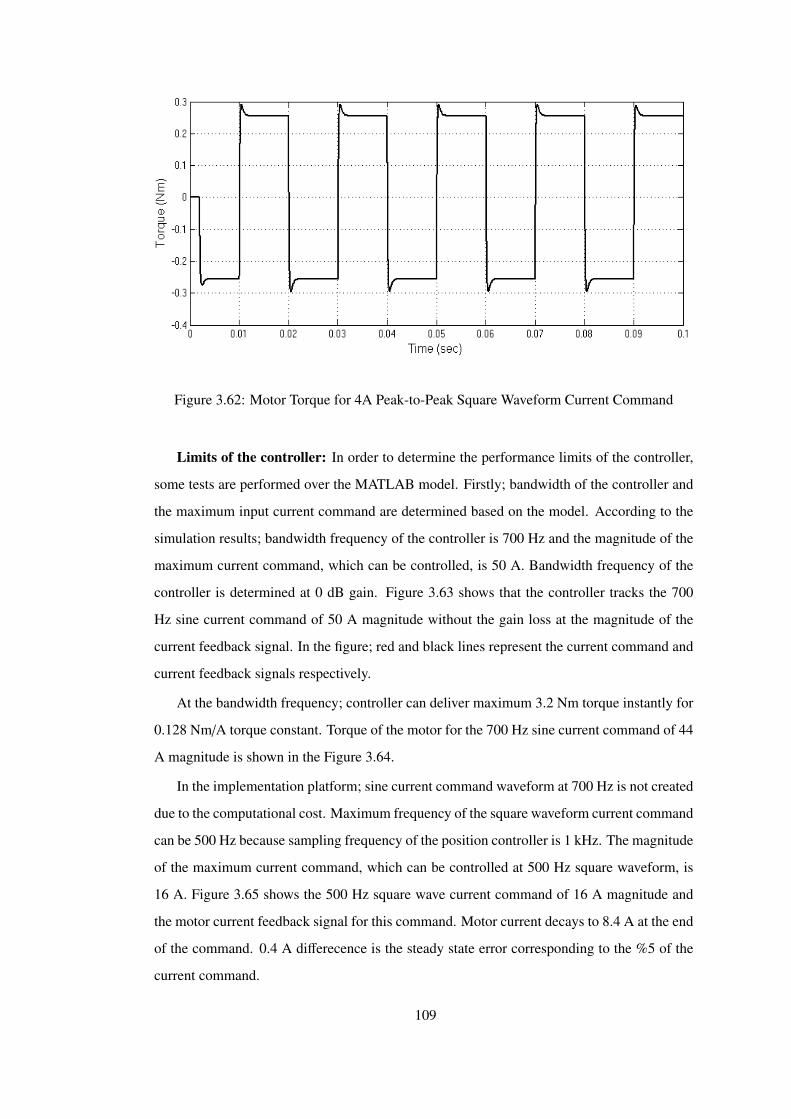
Figure 3.62: Motor Torque for 4A Peak-to-Peak Square Waveform Current Command
Limits of the controller: In order to determine the performance limits of the controller,
some tests are performed over the MATLAB model. Firstly; bandwidth of the controller and
the maximum input current command are determined based on the model. According to the
simulation results; bandwidth frequency of the controller is 700 Hz and the magnitude of the
maximum current command, which can be controlled, is 50 A. Bandwidth frequency of the
controller is determined at 0 dB gain. Figure 3.63 shows that the controller tracks the 700
Hz sine current command of 50 A magnitude without the gain loss at the magnitude of the
current feedback signal. In the figure; red and black lines represent the current command and
current feedback signals respectively.
At the bandwidth frequency; controller can deliver maximum 3.2 Nm torque instantly for
0.128 Nm/A torque constant. Torque of the motor for the 700 Hz sine current command of 44
A magnitude is shown in the Figure 3.64.
In the implementation platform; sine current command waveform at 700 Hz is not created
due to the computational cost. Maximum frequency of the square waveform current command
can be 500 Hz because sampling frequency of the position controller is 1 kHz. The magnitude
of the maximum current command, which can be controlled at 500 Hz square waveform, is
16 A. Figure 3.65 shows the 500 Hz square wave current command of 16 A magnitude and
the motor current feedback signal for this command. Motor current decays to 8.4 A at the end
of the command. 0.4 A differecence is the steady state error corresponding to the %5 of the
current command.
109

Figure 3.63: Current Command and Current Feedback Signals for a 700 Hz Sine CurrentCommand of 50 A Magnitude
Figure 3.64: Motor Torque for 700 Sine Current Command of 50 A Magnitude
110

Figure 3.65: Current Command and Current Feedback Signals for 500 Hz Square Wave Cur-rent Command of 16 A Magnitude
Gain of the controller is more than 0.4238 dB (1.05 of command) and current feedback
signal cannot settle to the current command during 1 msec when the magnitude of the current
command is larger than 16 A. In order to show this situation; 500 Hz square wave current
command of 20 A magnitude is applied to the controller model. Current command and feed-
back signals are shown in the Figure 3.66. As can be seen from the figure; current feedback
signal cannot settle to the current command of 10.5 A during the 1 ms.
Figure 3.66: Current Command and Current Feedback Signals for 500 Hz Square Wave Cur-rent Command of 20 A Magnitude
111

3.4 Experimental Results
To demonstrate the performance of the current controller, several tests are performed on the
control actuation system including four motors, BLM-25-7. Firstly; setup given in the Figure
2.18 is established. Results of the experiments are monitored on the GUI results window and
oscilloscope screen in parallel. The first two tests are done for observing the command track-
ing performance of the controller. After these; tests are done for analyzing the performance
of the controller in terms of overshoot, steady state error, rise time criteria.
Command Tracking Performance Test1: To avoid losing control of the current con-
troller, a square waveform with equal positive and minus portions is applied firstly to the
motors. Frequency of the current command waveform is 50 Hz and magnitude of it is 4A
peak to peak. Current feedback and current command signals on the GUI results window are
shown in the Figure 3.67. In this graph; red lines represent the current command, whereas
black ones represent the current feedback. In addition; oscilloscope view of feedback signal
is shown in the Figure 3.68. As can be seen from the Figure 3.67, current feedback signal
tracks the command signal effectively.
Figure 3.67: Current Command and Current Feedback Signals for a 50 Hz Square CurrentCommand of 4A Magnitude
The difference between the oscilloscope view and program window is the sampling rate.
112

Figure 3.68: Oscilloscope View of Current Feedback Signal for a 50 Hz Square CurrentCommand of 4A Magnitude
Sampling rate of the GUI program is 20 kS/s, but sampling rate of the oscilloscope is set to
the 200 MS/s for detecting the spike currents on the motor. Kp and TKI parameters of the
controller are determined as 50 and 6 respectively for this test.
In the Section 3.3; a 50 Hz square current command of 4A peak to peak magnitude is
applied to the motor. In addtion; current feedback and current command signals for this
command are given in the Figure 3.61. When the results of the simulation and experimental
tests are compared; it can be said that experimental results satisfy the simulation result.
Command Tracking Performance Test2: This test is performed for 25 Hz, 4A peak to
peak sine current command. Positive and minus portions of the waveform is set as equal for
preventing the motor from reaching the maximum speed. Current command of the controller
is composed of 8 step commands on the current command window of the GUI program. A
screenshot of the current command window is shown in the Figure 3.69.
Current feedback and current command signals on the GUI results window are shown in
the Figure 3.70. In addition; oscilloscope view of feedback signal is shown in the Figure 3.71.
113

Figure 3.69: Screen Shot of the 25 Hz Sine Current Command of 4A Magnitude
Figure 3.70: Current Command and Current feedback Signals for a 25 Hz Sine Current Com-mand of 4A Magnitude
As can be seen from the Figure 3.70, current feedback signal tracks the command signal
effectively. Aim of this test is to observe the performance of the controller under the varying
step commands. Duration of each step command is 5 ms.
114
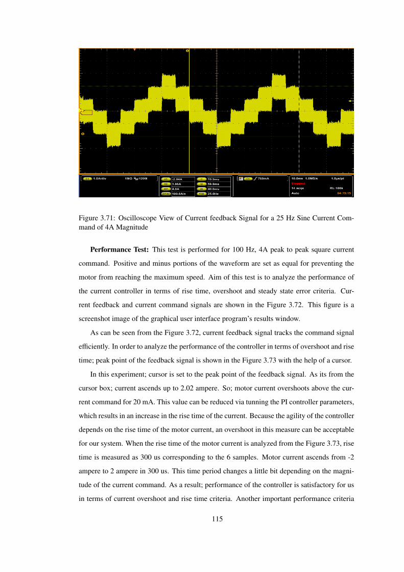
Figure 3.71: Oscilloscope View of Current feedback Signal for a 25 Hz Sine Current Com-mand of 4A Magnitude
Performance Test: This test is performed for 100 Hz, 4A peak to peak square current
command. Positive and minus portions of the waveform are set as equal for preventing the
motor from reaching the maximum speed. Aim of this test is to analyze the performance of
the current controller in terms of rise time, overshoot and steady state error criteria. Cur-
rent feedback and current command signals are shown in the Figure 3.72. This figure is a
screenshot image of the graphical user interface program’s results window.
As can be seen from the Figure 3.72, current feedback signal tracks the command signal
efficiently. In order to analyze the performance of the controller in terms of overshoot and rise
time; peak point of the feedback signal is shown in the Figure 3.73 with the help of a cursor.
In this experiment; cursor is set to the peak point of the feedback signal. As its from the
cursor box; current ascends up to 2.02 ampere. So; motor current overshoots above the cur-
rent command for 20 mA. This value can be reduced via tunning the PI controller parameters,
which results in an increase in the rise time of the current. Because the agility of the controller
depends on the rise time of the motor current, an overshoot in this measure can be acceptable
for our system. When the rise time of the motor current is analyzed from the Figure 3.73, rise
time is measured as 300 us corresponding to the 6 samples. Motor current ascends from -2
ampere to 2 ampere in 300 us. This time period changes a little bit depending on the magni-
tude of the current command. As a result; performance of the controller is satisfactory for us
in terms of current overshoot and rise time criteria. Another important performance criteria
115

Figure 3.72: Current Command and Current feedback Signals for a 100 Hz Square CurrentCommand of 4A Magnitude
Figure 3.73: Overshoot of Current Feedback Signal for a 100 Hz Square Current Commandof 4A Magnitude
116

of the current controller is steady state error, which affects the performance of the position
control loop. When the steady state error between the command and motor current is so high,
position controller increases the current command up to desired position. However; this pro-
cess decreases the agility of the performance of the position controller. In this experiment;
steady state error is measured as 50 mA, but this current error is not shown in the Figure
3.73. This error arises basically from some properties of magnetic current sensor, which are
the sensitivity error and temperature dependent offset currents. This error also could be min-
imized by increasing the integral gain parameter of the PI controller, but increase of integral
gain results in oscillation on the motor current.
Limits of the controller: In order to verify the performance limits of the controller;
some tests are performed over the implementation platform. As stated in the Matlab simu-
lations section; sine wave current command cannot be generated on the processor due to the
computational cost. So; current command waveform of these experimental tests is square and
its frequency is 500 Hz. Firstly; 500 Hz square wave current command of 16 A is applied
to the current controller and the motor current feedback (A) versus time (ms) is shown in the
Figure 3.74. As can be seen from the figure; current feedback signal rises from -8 A up to
10.2 A and settles to +8.4 A at the end of 1 ms. This test also verifies the related simulation
result.
Figure 3.74: Current Feedback Signal for a 500 Hz Square Current Command of 16A Mag-nitude (Experimental result)
According to the simulation results; controller cannot control 500 Hz square wave current
commands, magnitude of which is larger than 16 A magnitude. In order to verify the results
117

of the simulation tests; 500 Hz square wave current command of 20 A magnitude is applied to
the current controller and the current feedback signal for this command is shown in the Figure
3.75. As can be seen from the figure; current feedback signal rises from -10 A up to 12.7 A
and decays to 11.3 A at the end of 1 ms. So; steady state error, 1.3 A, is outside the limit of 5
percent. In contrast; value of the steady state error is 0.8 A in the simulation test. As a result;
it can be said that experimental test verifies the related simulation test.
Figure 3.75: Current Feedback Signal for a 500 Hz Square Current Command of 20A Mag-nitude (Experimental result)
In order to interpret the behavior of the current controller; square wave current commands
at different frequencies are applied to the controller and maximum current magnitude that
can be controlled is determined for the each applied command frequency. Figure 3.76 shows
the magnitude of the current command that can be controlled for the frequency of square
wave current command. As can be seen from the figure; maximum current magnitude 60 A
is obtained at 125 Hz square wave command. When the frequency of the command wave
is increased, magnitude of the current decreases due to the PI controller response and motor
dynamics (Inertia). However; back EMF voltage limits the magnitude of the current for the
lower frequencies because speed of the motor increases for the current commands, of which
frequency is lower than 125 Hz.
118
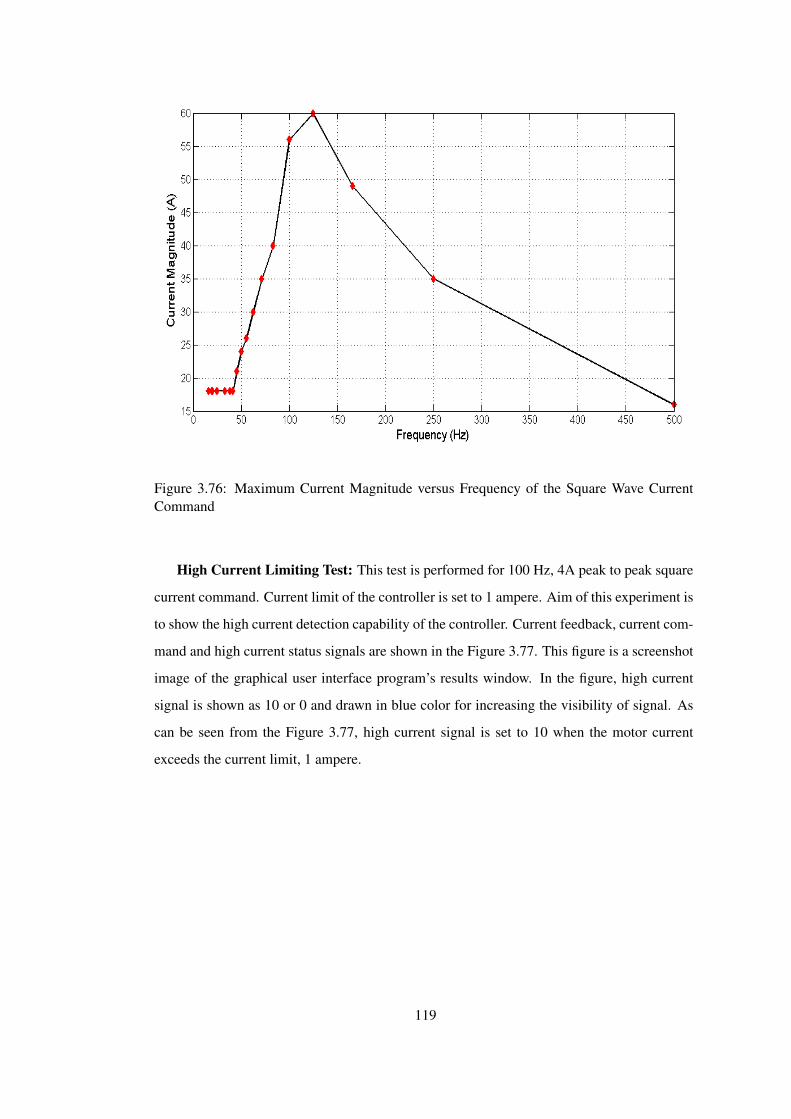
Figure 3.76: Maximum Current Magnitude versus Frequency of the Square Wave CurrentCommand
High Current Limiting Test: This test is performed for 100 Hz, 4A peak to peak square
current command. Current limit of the controller is set to 1 ampere. Aim of this experiment is
to show the high current detection capability of the controller. Current feedback, current com-
mand and high current status signals are shown in the Figure 3.77. This figure is a screenshot
image of the graphical user interface program’s results window. In the figure, high current
signal is shown as 10 or 0 and drawn in blue color for increasing the visibility of signal. As
can be seen from the Figure 3.77, high current signal is set to 10 when the motor current
exceeds the current limit, 1 ampere.
119
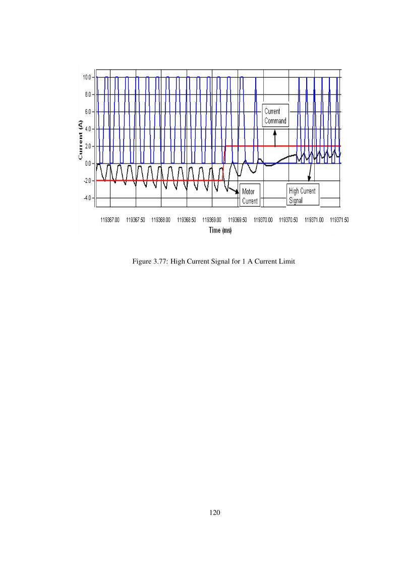
Figure 3.77: High Current Signal for 1 A Current Limit
120
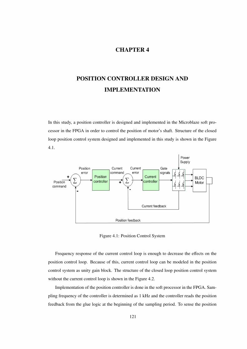
CHAPTER 4
POSITION CONTROLLER DESIGN AND
IMPLEMENTATION
In this study, a position controller is designed and implemented in the Microblaze soft pro-
cessor in the FPGA in order to control the position of motor’s shaft. Structure of the closed
loop position control system designed and implemented in this study is shown in the Figure
4.1.
Figure 4.1: Position Control System
Frequency response of the current control loop is enough to decrease the effects on the
position control loop. Because of this, current control loop can be modeled in the position
control system as unity gain block. The structure of the closed loop position control system
without the current control loop is shown in the Figure 4.2.
Implementation of the position controller is done in the soft processor in the FPGA. Sam-
pling frequency of the controller is determined as 1 kHz and the controller reads the position
feedback from the glue logic at the beginning of the sampling period. To sense the position
121

Figure 4.2: Position control system without the current control loop
of the motors’ shaft, encoders are used and a glue logic is coded in VHDL and implemented
in the FPGA for counting the pulses coming from the encoders. At the beginning of the
sampling period, position controller converts the pulse count to radian. Because the position
feedback is obtained and scaled in the same sampling period, position feedback block can be
considered as unity gain. New form of the position control system is shown in the Figure 4.3.
Figure 4.3: Position control system without the postion transducer
The motor mechanical equation is;
Tm = Jdwdt
+ Bw + TL (4.1)
Tm : Motor Torque (N − m)
TL : Load Torque (N − m)
w : Motor Speed (rad/sec)
J : Inertia (kg − m2)
B: Viscous Damping ( Nmrad/sec )
122

Substituting w = dΘdt , Equation 4.1 becomes
Kt.i = Jd2Θ
dt2 + BdΘ
dt+ TL (4.2)
When the Equation 4.2 is converted to the s domain, transfer function between the motor
current and motor position will be
Θ(s)i(s)
=Kt
Js2 + Bs(4.3)
New form of the position control system is shown in the Figure 4.4.
Figure 4.4: Position control system with the motor model
In this study; usage of the conventional controllers was preferred instead of the uncon-
ventional controllers due to implementation cost. P (Proportional), PI, PID (Proportional
Integral Derivative), PD (Proportional Derivative), I-PD (Integral Proportional Derivative)
controller topologies are examples for the conventional controllers. In contrast; fuzzy and
neuro-fuzzy controllers belong to the unconventional controllers. Because of conventional
controllers’s simplicity, they are backbones of many complex control systems. PID and I-
PD controller topologies are mainly focused based on the controller design section of the Ali
YILMAZKOCLAR’s thesis study, name of which is Brushless DC motor position control for
a control actuation system [1].
123
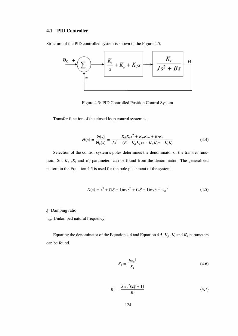
4.1 PID Controller
Structure of the PID controlled system is shown in the Figure 4.5.
Figure 4.5: PID Controlled Position Control System
Transfer function of the closed loop control system is;
H(s) =Θ(s)Θc(s)
=KdKt s2 + KpKt s + KiKt
Js3 + (B + KdKt)s + KpKt s + KiKt(4.4)
Selection of the control system’s poles determines the denominator of the transfer func-
tion. So; Kp ,Ki and Kd parameters can be found from the denominator. The generalized
pattern in the Equation 4.5 is used for the pole placement of the system.
D(s) = s3 + (2ξ + 1)wns2 + (2ξ + 1)wns + wn3 (4.5)
ξ: Damping ratio;
wn: Undamped natural frequency
Equating the denominator of the Equation 4.4 and Equation 4.5, Kp, Ki and Kd parameters
can be found.
Ki =Jwn
3
Kt(4.6)
Kp =Jwn
2(2ξ + 1)Kt
(4.7)
124
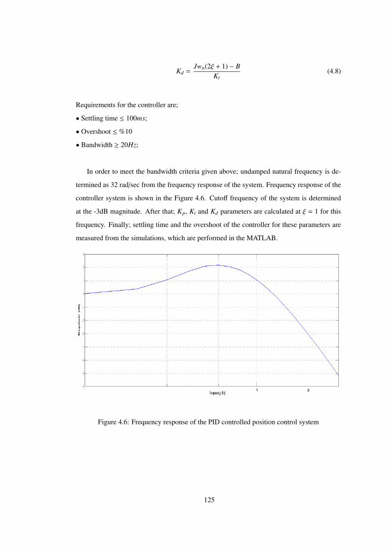
Kd =Jwn(2ξ + 1) − B
Kt(4.8)
Requirements for the controller are;
• Settling time ≤ 100ms;
• Overshoot ≤ %10
• Bandwidth ≥ 20Hz;
In order to meet the bandwidth criteria given above; undamped natural frequency is de-
termined as 32 rad/sec from the frequency response of the system. Frequency response of the
controller system is shown in the Figure 4.6. Cutoff frequency of the system is determined
at the -3dB magnitude. After that; Kp, Ki and Kd parameters are calculated at ξ = 1 for this
frequency. Finally; settling time and the overshoot of the controller for these parameters are
measured from the simulations, which are performed in the MATLAB.
Figure 4.6: Frequency response of the PID controlled position control system
125

System parameters for the wn=32 (rad/sec) and ξ = 1 are shown in the Table 4.1. These
parameters satisfy the bandwidth requirement, but don’t meet the settling time and overshoot
requirements. In the MATLAB Simulations section, simulation results for these system pa-
rameters are provided and analyzed in terms of performance criteria.
Table 4.1: PID System Parameters for ξ = 1
ξ Kp Ki Kd wn (rad/sec) Settling time (ms) Overshoot1 1.744 18.6 0.05 32 350 %25
Implementation Algorithm: PID controller is coded in the programming language C
and run over the Microblaze soft processor. Implementation algorithm of the controller is
1-) Read the motor position register from the encoder interface module.
2-) Convert the position register value to the rad/sec by multiplying the (2*pi) /4096 constant.
3-) Calculate the position error by subtracting the position feedback from the position com-
mand.
4-) Add the position error to the integral term.
5-) Limit the integral term at the PID−Limit/ Ki.
6-) Subtract the previous error from the present error.
7-) Calculate the proportional, integral and derivative gains.
8-) Calculate the sum of the proportional, integral and derivative gains.
9-) Limit the sum value at the PID−Limit (30) constant.
10-) Update the previous error with the present one.
126

4.2 I-PD Controller
As stated in the PID controller design section; controller does not satisfy the requirements
defined for the performance criteria. In addition; this is also shown via simulation results in
the Section 4.4. An I-PD controller is designed for our system due to the reasons, which are
the PID controller’s insufficiency and the proven performance of the I-PD controller in the Ali
YILMAZKOCLAR’s thesis study [1]. In this controller topology; proportional and derivative
actions are moved to the feedback path so that high initial values at the output of the controller
are avoided. Structure of the I-PD controlled system is shown in the Figure 4.7.
Figure 4.7: IPD Controlled Position Control System
Transfer function of the I-PD controlled position control system is given in the Equation
4.9.
H(s) =Θ(s)Θc(s)
=KiKt
Js3 + (B + KdKt)s + KpKt s + KiKt(4.9)
In order to remember the requirements of the controller, they are provided again in the
below.
Requirements for the controller are;
• Settling time ≤ 100ms;
• Overshoot ≤ %10
• Bandwidth ≥ 20Hz;
The generalized pattern in the Equation 4.10 is used for the pole placement of the system.
Because the denominators of the PID and I-PD controllers’ transfer functions are same, this
generalized pattern can also be used for this system. So, equating the denominator of the
transfer function and generalized pattern, same Kp, Ki and Kd equations, which are provided
in the Section 4.1, can be obtained.
127
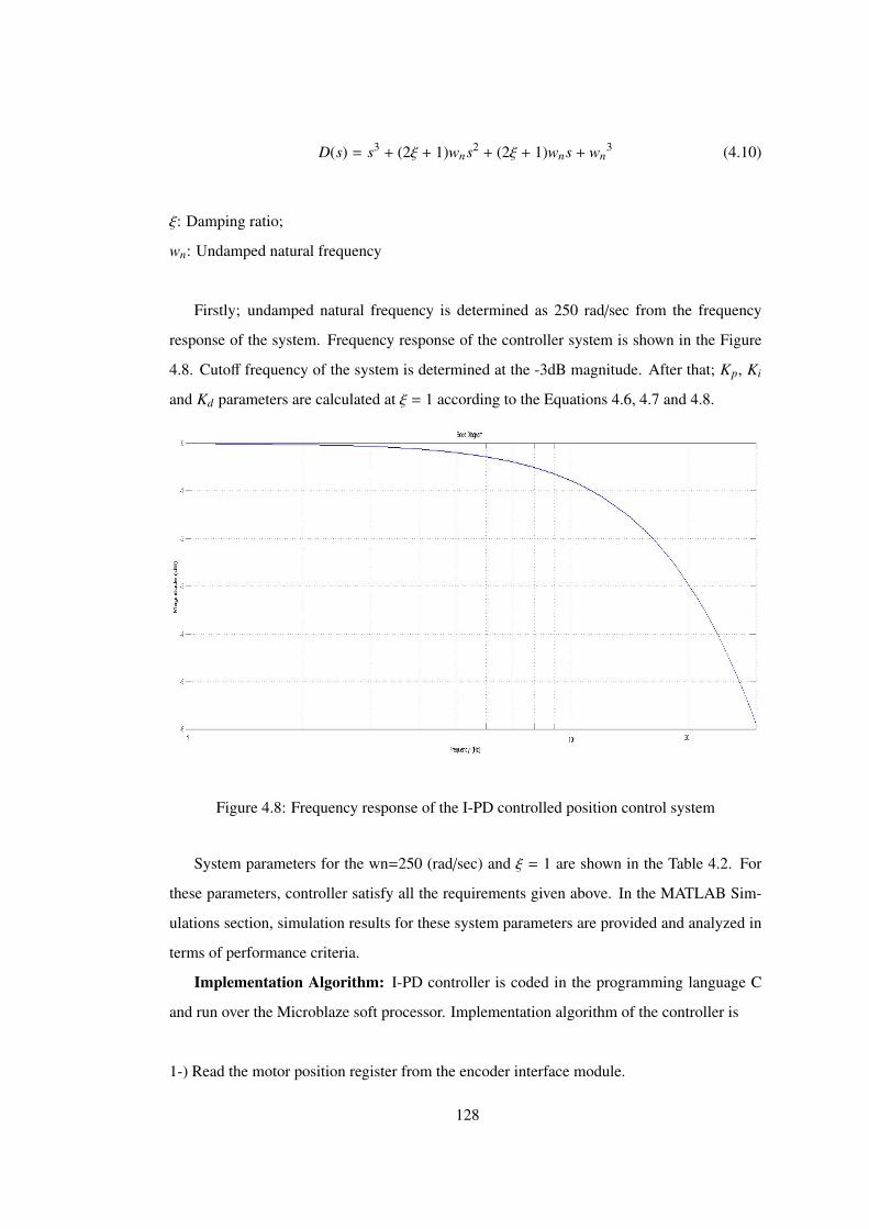
D(s) = s3 + (2ξ + 1)wns2 + (2ξ + 1)wns + wn3 (4.10)
ξ: Damping ratio;
wn: Undamped natural frequency
Firstly; undamped natural frequency is determined as 250 rad/sec from the frequency
response of the system. Frequency response of the controller system is shown in the Figure
4.8. Cutoff frequency of the system is determined at the -3dB magnitude. After that; Kp, Ki
and Kd parameters are calculated at ξ = 1 according to the Equations 4.6, 4.7 and 4.8.
Figure 4.8: Frequency response of the I-PD controlled position control system
System parameters for the wn=250 (rad/sec) and ξ = 1 are shown in the Table 4.2. For
these parameters, controller satisfy all the requirements given above. In the MATLAB Sim-
ulations section, simulation results for these system parameters are provided and analyzed in
terms of performance criteria.
Implementation Algorithm: I-PD controller is coded in the programming language C
and run over the Microblaze soft processor. Implementation algorithm of the controller is
1-) Read the motor position register from the encoder interface module.
128

Table 4.2: I-PD System Parameters for ξ = 1
ξ Kp Ki Kd wn (rad/sec) Settling time (ms) Overshoot1 106.49 8874.5 0.426 250 40 %0
2-) Convert the position register value to the rad/sec by multiplying the (2*pi) /4096 constant.
3-) Calculate the position error by subtracting the position feedback from the position com-
mand.
4-) Add the position error to the integral term.
5-) Subtract the previous position from the present position.
6-) Calculate the proportional, integral and derivative gains.
7-) Subtract the derivative and proportional gains from the integral gain.
8-) Limit the I-PD value at the IPD−Limit (30) constant.
9-) Update the previous position with the present one.
129
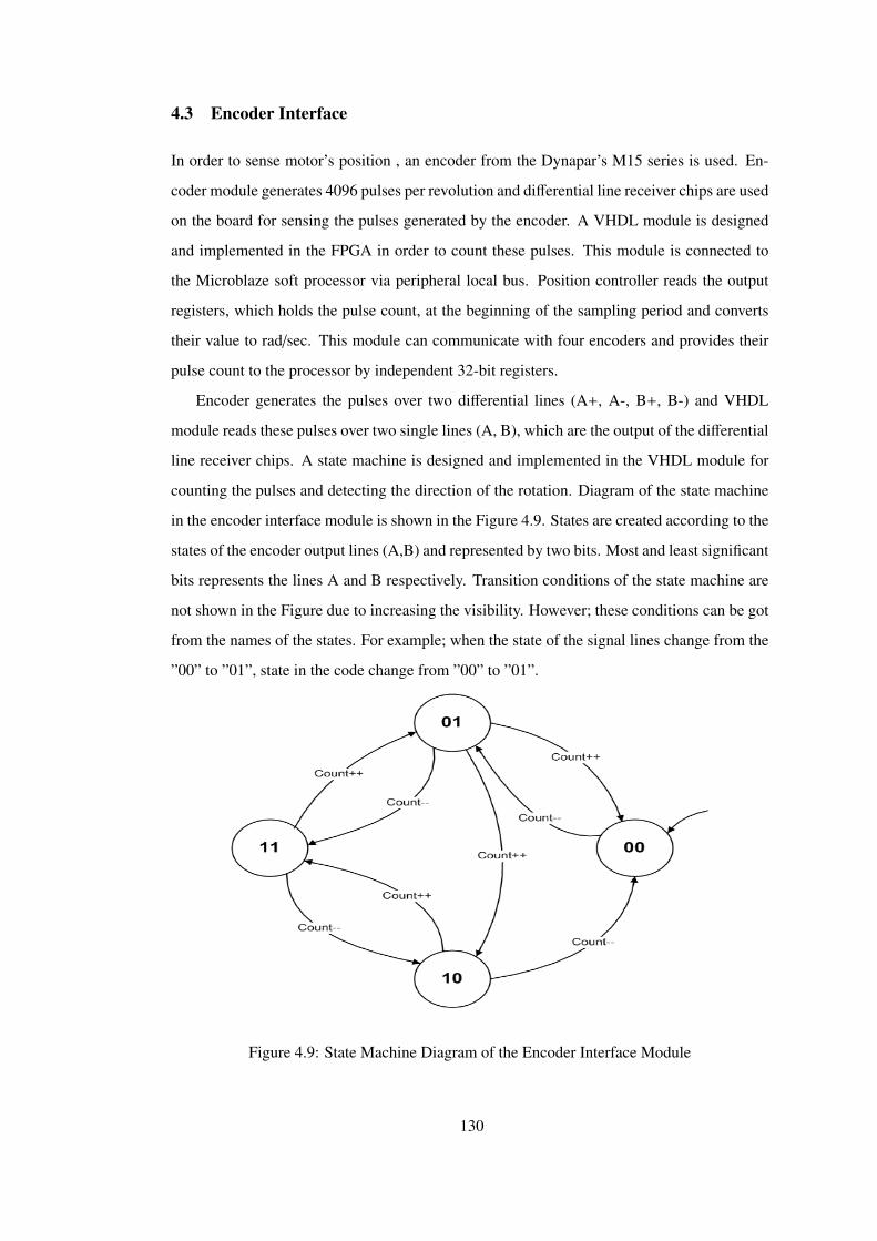
4.3 Encoder Interface
In order to sense motor’s position , an encoder from the Dynapar’s M15 series is used. En-
coder module generates 4096 pulses per revolution and differential line receiver chips are used
on the board for sensing the pulses generated by the encoder. A VHDL module is designed
and implemented in the FPGA in order to count these pulses. This module is connected to
the Microblaze soft processor via peripheral local bus. Position controller reads the output
registers, which holds the pulse count, at the beginning of the sampling period and converts
their value to rad/sec. This module can communicate with four encoders and provides their
pulse count to the processor by independent 32-bit registers.
Encoder generates the pulses over two differential lines (A+, A-, B+, B-) and VHDL
module reads these pulses over two single lines (A, B), which are the output of the differential
line receiver chips. A state machine is designed and implemented in the VHDL module for
counting the pulses and detecting the direction of the rotation. Diagram of the state machine
in the encoder interface module is shown in the Figure 4.9. States are created according to the
states of the encoder output lines (A,B) and represented by two bits. Most and least significant
bits represents the lines A and B respectively. Transition conditions of the state machine are
not shown in the Figure due to increasing the visibility. However; these conditions can be got
from the names of the states. For example; when the state of the signal lines change from the
”00” to ”01”, state in the code change from ”00” to ”01”.
Figure 4.9: State Machine Diagram of the Encoder Interface Module
130

4.4 Matlab Simulations
In order to measure the performance of the PID and I-PD controllers for the derived set of
poles and zeros, simulations of the controllers with the motor model are made in the Simulink
platform of the MATLAB. According to the simulation results, PID controller does not meet
the requirements for the system parameters available in the Table 4.1. In contrast; simulation
results of the I-PD controller show that I-PD controller position control system satisfies the
requirements given in the previous sections. Matlab model of the I-PD controller is only
provided in the thesis because PID controller does not satisfy the requirements. Model of the
controller is shown in the Figure 4.10. Sampling delays of the position command and position
feedback signals are taken into account in the model and they are modeled by transport delay
blocks of the simulink platform. In addition; rate limiter block is used in the command path
in order to limit rise of the step commands. This block is also implemented in the Microblaze
soft processor. To obtain a more realistic model; current controller Simulink model is also
used in the model.
131

Figure 4.10: Matlab Model of the I-PD Position Control System
132

PID Controller Step Command Response: This test is performed for 300 degree step
command and Kp, Ki and Kd parameters of the PID controller are set to the parameters given
in the Table 4.1. Step response of the controller is shown in the Figure 4.11. As can be seen
from the graph, settling time is approximately 350 ms and overshoot is % 25. Thus; these
control parameters don’t satisfy the requirements of maximum overshoot and settling time.
Output of the PID controller, which is current command, is shown in the Figure 4.12.
Figure 4.11: Step response of the PID controlled system for 300 degree command
Output of the PID controller is limited at +30 A and -30 A for preventing the high-valued
current flows on the board and the motor. As can be seen from the Figure 4.12, initial value
of the current command is 30 A, which is another handicap of the PID controller. This figure
also shows that the current command decreases to 0 when the motor reaches to the desired
position.
133
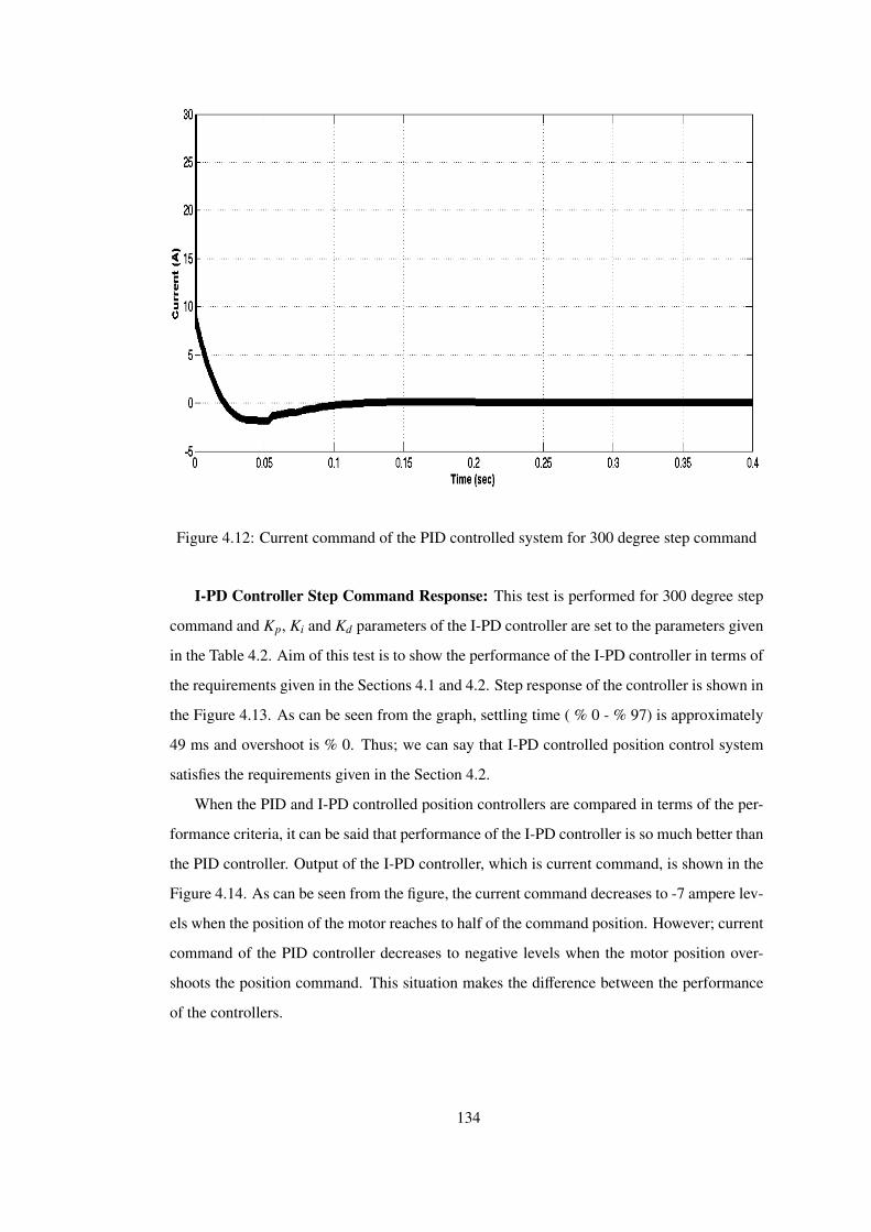
Figure 4.12: Current command of the PID controlled system for 300 degree step command
I-PD Controller Step Command Response: This test is performed for 300 degree step
command and Kp, Ki and Kd parameters of the I-PD controller are set to the parameters given
in the Table 4.2. Aim of this test is to show the performance of the I-PD controller in terms of
the requirements given in the Sections 4.1 and 4.2. Step response of the controller is shown in
the Figure 4.13. As can be seen from the graph, settling time ( % 0 - % 97) is approximately
49 ms and overshoot is % 0. Thus; we can say that I-PD controlled position control system
satisfies the requirements given in the Section 4.2.
When the PID and I-PD controlled position controllers are compared in terms of the per-
formance criteria, it can be said that performance of the I-PD controller is so much better than
the PID controller. Output of the I-PD controller, which is current command, is shown in the
Figure 4.14. As can be seen from the figure, the current command decreases to -7 ampere lev-
els when the position of the motor reaches to half of the command position. However; current
command of the PID controller decreases to negative levels when the motor position over-
shoots the position command. This situation makes the difference between the performance
of the controllers.
134

Figure 4.13: Step response of the I-PD controlled system for 300 degree step command
Figure 4.14: Current command of the I-PD controlled system for 300 degree step command
135
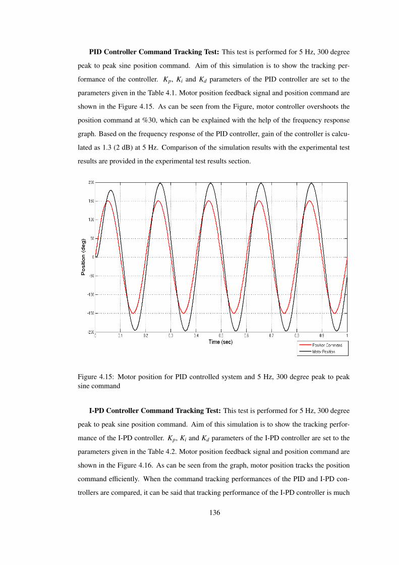
PID Controller Command Tracking Test: This test is performed for 5 Hz, 300 degree
peak to peak sine position command. Aim of this simulation is to show the tracking per-
formance of the controller. Kp, Ki and Kd parameters of the PID controller are set to the
parameters given in the Table 4.1. Motor position feedback signal and position command are
shown in the Figure 4.15. As can be seen from the Figure, motor controller overshoots the
position command at %30, which can be explained with the help of the frequency response
graph. Based on the frequency response of the PID controller, gain of the controller is calcu-
lated as 1.3 (2 dB) at 5 Hz. Comparison of the simulation results with the experimental test
results are provided in the experimental test results section.
Figure 4.15: Motor position for PID controlled system and 5 Hz, 300 degree peak to peaksine command
I-PD Controller Command Tracking Test: This test is performed for 5 Hz, 300 degree
peak to peak sine position command. Aim of this simulation is to show the tracking perfor-
mance of the I-PD controller. Kp, Ki and Kd parameters of the I-PD controller are set to the
parameters given in the Table 4.2. Motor position feedback signal and position command are
shown in the Figure 4.16. As can be seen from the graph, motor position tracks the position
command efficiently. When the command tracking performances of the PID and I-PD con-
trollers are compared, it can be said that tracking performance of the I-PD controller is much
136
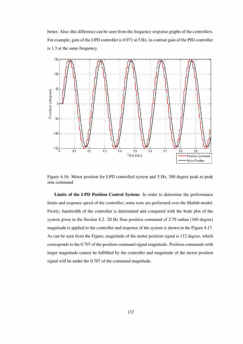
better. Also; this difference can be seen from the frequency response graphs of the controllers.
For example; gain of the I-PD controller is 0.971 at 5 Hz, in contrast gain of the PID controller
is 1.3 at the same frequency.
Figure 4.16: Motor position for I-PD controlled system and 5 Hz, 300 degree peak to peaksine command
Limits of the I-PD Position Control System: In order to determine the performance
limits and response speed of the controller; some tests are performed over the Matlab model.
Firstly; bandwidth of the controller is determined and compared with the bode plot of the
system given in the Section 4.2. 20 Hz Sine position command of 2.79 radian (160 degree)
magnitude is applied to the controller and response of the system is shown in the Figure 4.17.
As can be seen from the Figure; magnitude of the motor position signal is 112 degree, which
corresponds to the 0.707 of the position command signal magnitude. Position commands with
larger magnitude cannot be fullfilled by the controller and magnitude of the motor position
signal will be under the 0.707 of the command magnitude.
137
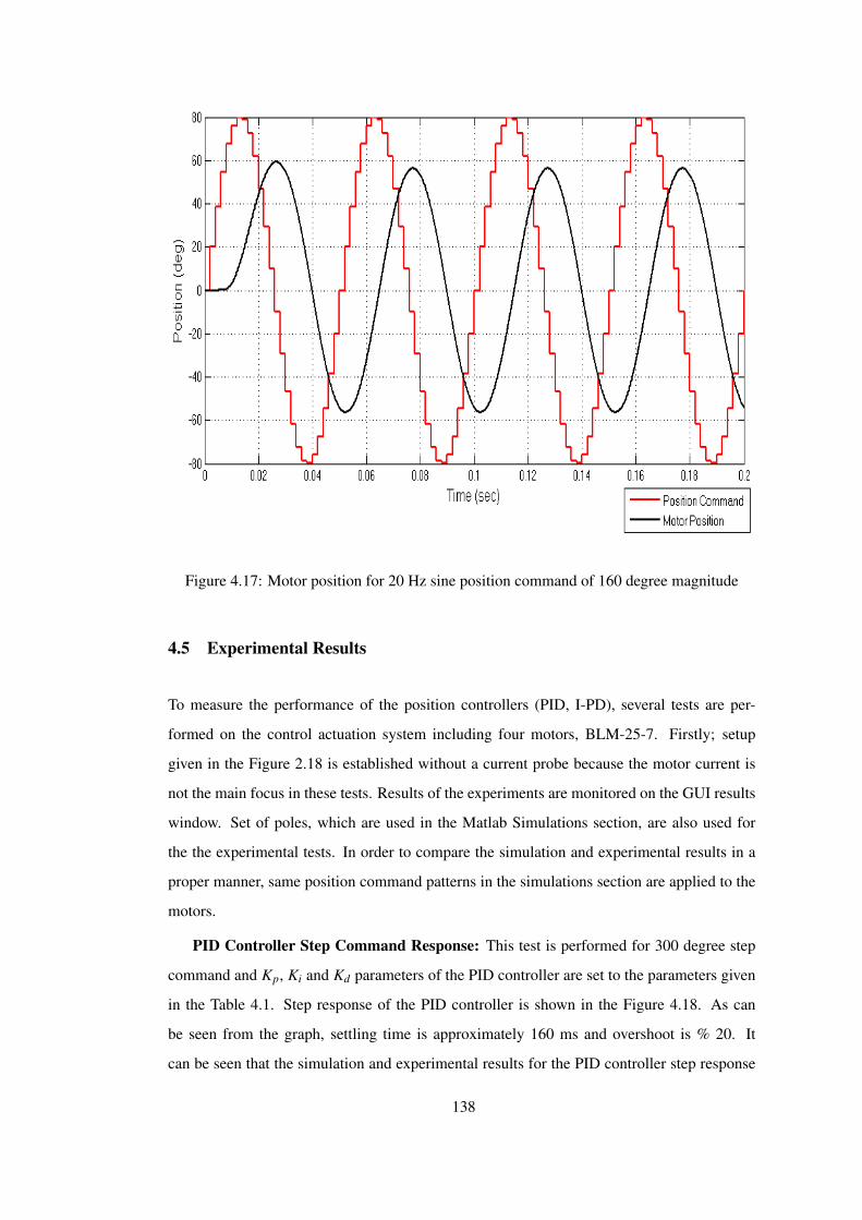
Figure 4.17: Motor position for 20 Hz sine position command of 160 degree magnitude
4.5 Experimental Results
To measure the performance of the position controllers (PID, I-PD), several tests are per-
formed on the control actuation system including four motors, BLM-25-7. Firstly; setup
given in the Figure 2.18 is established without a current probe because the motor current is
not the main focus in these tests. Results of the experiments are monitored on the GUI results
window. Set of poles, which are used in the Matlab Simulations section, are also used for
the the experimental tests. In order to compare the simulation and experimental results in a
proper manner, same position command patterns in the simulations section are applied to the
motors.
PID Controller Step Command Response: This test is performed for 300 degree step
command and Kp, Ki and Kd parameters of the PID controller are set to the parameters given
in the Table 4.1. Step response of the PID controller is shown in the Figure 4.18. As can
be seen from the graph, settling time is approximately 160 ms and overshoot is % 20. It
can be seen that the simulation and experimental results for the PID controller step response
138
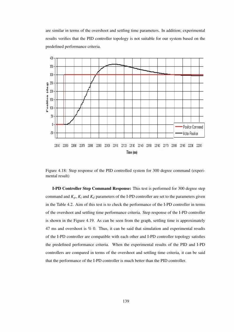
are similar in terms of the overshoot and settling time parameters. In addition; experimental
results verifies that the PID controller topology is not suitable for our system based on the
predefined performance criteria.
Figure 4.18: Step response of the PID controlled system for 300 degree command (experi-mental result)
I-PD Controller Step Command Response: This test is performed for 300 degree step
command and Kp, Ki and Kd parameters of the I-PD controller are set to the parameters given
in the Table 4.2. Aim of this test is to check the performance of the I-PD controller in terms
of the overshoot and settling time performance criteria. Step response of the I-PD controller
is shown in the Figure 4.19. As can be seen from the graph, settling time is approximately
47 ms and overshoot is % 0. Thus, it can be said that simulation and experimental results
of the I-PD controller are compatible with each other and I-PD controller topology satisfies
the predefined performance criteria. When the experimental results of the PID and I-PD
controllers are compared in terms of the overshoot and settling time criteria, it can be said
that the performance of the I-PD controller is much better than the PID controller.
139

Figure 4.19: Step response of the I-PD controlled system for 300 degree command (experi-mental result)
PID Controller Command Tracking Test: This test is performed for 5 Hz, 300 degree
peak to peak sine position command. Aims of this simulation is to show the tracking per-
formance of the controller. Kp, Ki and Kd parameters of the PID controller are set to the
parameters given in the Table 4.1. Motor position feedback signal and position command
are shown in the Figure 4.20. As can be seen from the Figure, motor controller overshoots
the position command at %30, which can be explained with the help of the frequency re-
sponse graph (Figure 4.6). Based on the frequency response of the PID controller, gain of the
controller is calculated as 1.3 (2 dB) at 5 Hz.
I-PD Controller Command Tracking Test: This test is performed for 5 Hz, 300 degree
peak to peak sine position command. Aim of this simulation is to show the tracking perfor-
mance of the I-PD controller. Kp, Ki and Kd parameters of the I-PD controller are set to the
parameters given in the Table 4.2. Motor position feedback signal and position command are
shown in the Figure 4.21. As can be seen from the graph, motor position tracks the posi-
tion command efficiently. Also; it can be said that experimental results satisfy the simulation
results.
140

Figure 4.20: Motor position for PID controlled system and 5 Hz, 300 degree peak to peaksine command (experimental result)
Figure 4.21: Motor position for I-PD controlled system and 5 Hz, 300 degree peak to peaksine command (experimental result)
141
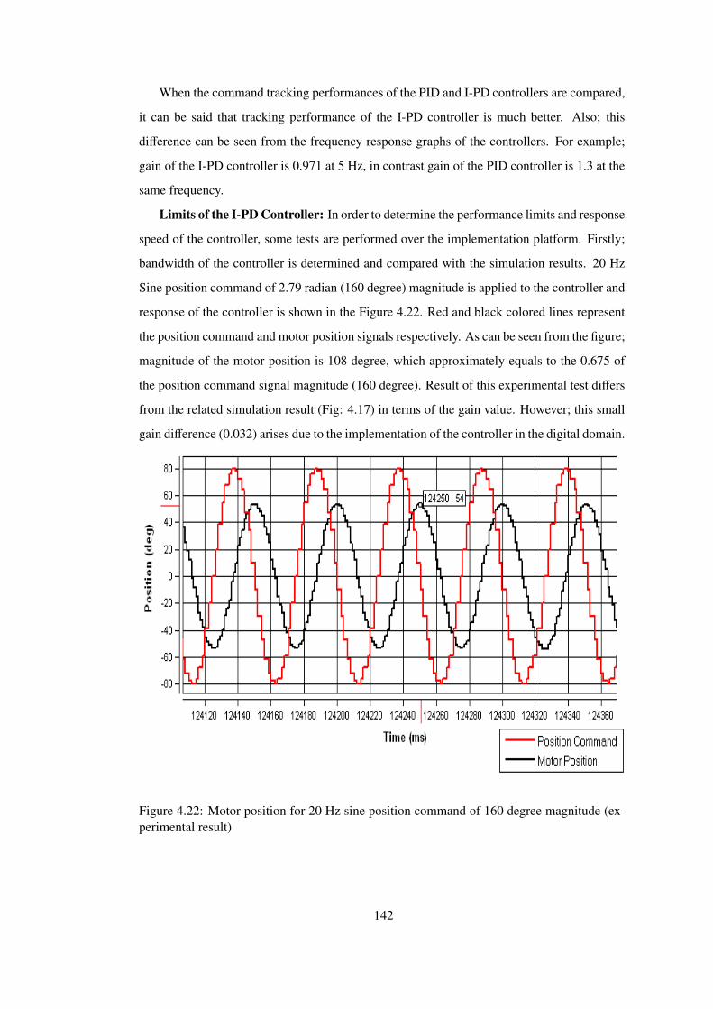
When the command tracking performances of the PID and I-PD controllers are compared,
it can be said that tracking performance of the I-PD controller is much better. Also; this
difference can be seen from the frequency response graphs of the controllers. For example;
gain of the I-PD controller is 0.971 at 5 Hz, in contrast gain of the PID controller is 1.3 at the
same frequency.
Limits of the I-PD Controller: In order to determine the performance limits and response
speed of the controller, some tests are performed over the implementation platform. Firstly;
bandwidth of the controller is determined and compared with the simulation results. 20 Hz
Sine position command of 2.79 radian (160 degree) magnitude is applied to the controller and
response of the controller is shown in the Figure 4.22. Red and black colored lines represent
the position command and motor position signals respectively. As can be seen from the figure;
magnitude of the motor position is 108 degree, which approximately equals to the 0.675 of
the position command signal magnitude (160 degree). Result of this experimental test differs
from the related simulation result (Fig: 4.17) in terms of the gain value. However; this small
gain difference (0.032) arises due to the implementation of the controller in the digital domain.
Figure 4.22: Motor position for 20 Hz sine position command of 160 degree magnitude (ex-perimental result)
142

Response of the controller is also tested and determined for different frequencies. Fre-
quency of the sine position command is increased by two from zero up to twenty Hz and
maximum magnitude of the position command is measured for the ten different sample points.
Figure 4.23 shows the magnitude of the position command versus frequency of the sine com-
mand frequency. As can be seen from the figure; controller can respond to position command
of 3.54 radian magnitude at 20 Hz and magnitude of the command increases up to 89 radian
as the frequency of the command decays to 1 Hz. Experimental results are also verified by
the simulation results.
Figure 4.23: Magnitude of the position command versus frequency of the sine wave positioncommand
143
CHAPTER 5
CONCLUSION
The purpose of this thesis was to develop a flexible, configurable, compact and high-performance
brushless DC motor control system. Although the system was not designed for a project of
TUBITAK-SAGE, it can be adapted to a control actuation system of a guided munition in
future. In addition; the techniques used in this study can be adapted to another motor control
system.
To design a compact motor control system was one of the goals of this study, because
volume and weight of the components are very important for a lot of systems. To succeed
this goal, this study is based on the system on chip concept. Current and position controllers
are implemented in a single FPGA chip in the scope of this concept. Besides these con-
trollers, position sensor interface modules and some communication modules such as UART
and Spacewire are also implemented in the same FPGA chip. In this study; soft processor
technology is also used due to its benefits, such as configurability and flexibility. Position
controller and UART packet controller are implemented in the soft processor in the FPGA.
In order to increase the configurability and flexibility of the system, configuration registers,
which can be accessed by the processor, were put in the current controller VHDL module. By
this way; this design can be adapted to other motor models easily.
In order to measure and verify the performance of the design, a graphical user interface
program was designed within the scope of this study. User interface program communicates
with the board over UART and Spacewire communication protocols. Because the Spacewire
protocol provides a high-speed communication link, user can monitor the behavior of the con-
trollers in real time graphically. In addition to these; user can configure the controllers quickly
and create input patterns for the controllers with the help of this user interface program.
An electronic board was designed and manufactured within the scope of this thesis. Pro-
144

duction and placement process costs of the board were met by the TUBITAK-SAGE. Board
includes the digital and power electronic circuitries together. FPGA design was implemented
and tested in this board. However; this FPGA design can be moved to another FPGA chip or
board easily.
In order to increase the flexibility of the system, recommended future works are listed
below:
• In the present current controller VHDL module, pulse width modulation frequency is
set to a fixed value 20 kHz and this modulation frequency is satisfactory for many actuation
systems. However; modulation frequency of the current controller can be changeable by the
user for increasing the flexibility. Also; sampling rate of the controller must be changed
automatically according to the new modulation frequency.
• In the present current controller VHDL module, analog to digital converter VHDL driver
part was developed for the chips on the board. This part of the controller communicates with
the ADC chips via SPI protocol and gets the outputs of the chips in a proper manner. Ac-
tually; this driver code works with different models of ADC chips from different companies.
However; this part of the controller may be more general for increasing the flexibility of the
system.
• There are different multiple methods of pulse width modulation in the literature. Pulse
width modulation technique determines the mosfets to be activated during the operating cycle.
Present controller supports one type of these methods, which is the best one in terms of power
consumption. Flexibility of the controller will increase if the controller supports other pulse
width modulation techniques. Also; this could be done via putting new commutation look-up
tables into the commutation control module. Also; these tables must be selectable from the
graphical user interface program.
In order to improve the performance of the current and position controllers, recommended
future works are listed below:
• In the present system; integral gain of the PI controller in the current controller can take
integer values between 0 and 31. However; increasing the range and resolution of the integral
gain would be useful for the performance of the current controller.
• Performance of the current controller can be improved a little by increasing the present
current sampling rate, 1.3 MSPS. However; this will increase the complexity of the FPGA
design and require high-speed ADC chips.
• In the present position control system; frequency bandwidth of the control system is set
145

to 20 Hz. However; increasing the bandwidth frequency at an acceptable level would improve
the performance of the system.
• In the present position control system; sampling frequency is set to 1 kHz and software
of the processor is coded according to this frequency value. However; agility of the position
controller can be improved by increasing the value of sampling and bandwidth frequencies.
Taking into account the limits of the processor, software can be updated for this operation.
146

REFERENCES
[1] Ali Yılmazkoclar. Brushless DC motor position control for a control actuation system.Master’s thesis, Middle East Technical University, September 2002.
[2] Fernando Rodriguez. A novel digital control technique for brushless DC motor drives.IEEE Transactions on Industrial Electronics, Vol. 54, No. 5, October 2007.
[3] Dejan Kos, Milan Curkovic, and Karel Jezernik. FPGA based BLDC motor current con-trol with spectral analysis Power Electronics and Motion Control Conference, Septem-ber 2006.
[4] Dayu Wang, Kaiping Yu, Hong Guo. Functional design of FPGA in a brushless DC mo-tor system based on FPGA and DSP. IEEE Vehicle Power and Propulsion Conference,September 3-5, 2008.
[5] Xiaoyin Shao and Dong Sun. An FPGA based motion control IC and its application torobotic manipulators. International Conference on Control, Automation, Robotics andVision, 2006.
[6] 0. Al-Ayasrah, T. Alukaidey, G. Pissanidis. DSP based N-Motor speed control of brush-less DC motors using external FPGA design. IEEE International Conference on Indus-trial Technology, Page(s): 627 - 631, 2006.
[7] Ying-Yu Tzou. Design and implementation of an FPGA-Based motor control IC forpermanent magnet AC servo motors. Industrial Electronics on Control and Instrumen-tation, Vol.2, Page(s): 943 - 947, 1997.
[8] Charlie Ice, Bilal Akin. Designing High-Performance and Power-Efficient Motor Con-trol Systems. Texas Instruments, June 2009.
[9] Jung Uk Cho, Quy Ngoc Le, and Jae Wook Jeon. An FPGA-Based multiple-axis motioncontrol chip IEEE Transactions on Industrial Electronics, Vol. 56, No. 3, March 2009.
[10] Toshio Takahashi, Jay Goetz. Implementation of complete AC servo control in a lowcost FPGA and subsequent ASSP conversion. IEEE Applied Power Electronics Confer-ence and Exposition, Vol. 1, Page(s): 565 - 570, February 2004.
[11] Geir Kjosavik. Take Electronic Motor Drives to the Next Level. Xilinx, September2005.
[12] FalconEye Reference Design. Motion Control Reference Design Platform for BrushlessMotors . FalconEye, September 2007.
[13] Xilinx Datasheet. Spartan-3 FPGA Family Datasheet. Xilinx, June 2008.
[14] Analog Devices Datasheet. Quad Channel Digital Isolators. Analog Devices, May 2008.
147

[15] European Space Agency. Spacewire Standard Available fromhttp://www.spacewire.esa.int/content/ Standard/Standard.php. European SpaceAgency, Accessed 20th August 2011.
[16] LEM Datasheet. Current Transducer CKSR series. LEM, Version 5.
[17] Xilinx Reference Guide. Microblaze Processor Reference Guide. Xilinx, UG081(V8.1), October 2007.
[18] STAR Dundee Users Manual. SpaceWire Brick Hardware Users Manual. STARDundee, UoD Brick User (V1.0), August 2004.
[19] Analog Devices Datasheet. AD7944 Datasheet. Analog Devices, October 2009.
148