Embed Size (px)
Citation preview
An FPGA Based High Speed IEEE-754
Double Precision Floating Point Multiplier
U sing Verilog
Addanki Puma Rameshl, A. V. N. Tilak2, A.M.Prasad3
ISri Yasavi Engineering College, Pedatadepalli, 2Y.R.Siddhartha Engineering College, Kanuru,3 UCEK JNTU, 1 Tadepalligudem, 2Yijayawada, 3Kakinada,I,2,3India.
[email protected],[email protected], 3a _ [email protected]
Abstract- Floating Point (FP) mUltiplication is widely
used in large set of scientific and signal processing computation. Multiplication is one of the common arithmetic operations in these computations. A high speed floating point double precision multiplier is
implemented on a Virtex-6 FPGA. In addition, the
proposed design is compliant with IEEE-754 format and handles over flow, under flow, rounding and various exception conditions. The design achieved the operating
frequency of 414.714 MHz with an area of 648 slices.
Keywords- Double precision, Floating point, Multiplier,
FPGA,IEEE-754.
I. INTRODUCTION
The real numbers represented in binary format are known as floating point numbers. Based on TEEE-754 standard, floating point formats are classified into binary and decimal interchange formats. Floating point multipliers are very important in DSP applications.
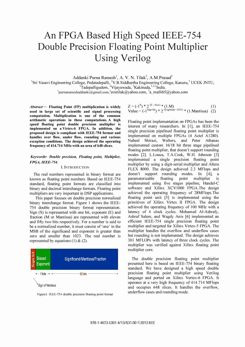
This paper focuses on double precision normalized binary interchange format. Figure I shows the TEEE-754 double precision binary format representation. Sign (S) is represented with one bit, exponent (E) and fraction (M or Mantissa) are represented with eleven and fifty two bits respectively. For a number is said to be a normalized number, it must consist of 'one' in the MSB of the significand and exponent is greater than zero and smaller than 1023. The real number is represented by equations (I) & (2).
Sig n of Mantissa
Figurel. TEEE-754 double precision floating point format
Z = (-I S) * 2 (E - Ria.l) * (1. M) (1 )
Yalue = (-I Sign bit) * 2 (Exponent -1023) * (I.Mantissa) (2)
Floating point implementation on FPGAs has been the interest of many researchers. In [I], an TEEE-754 single precision pipelined floating point multiplier is implemented on multiple FPGAs (4 Actel AI280). Nabeel Shirazi, Walters, and Peter Athanas implemented custom 16/18 bit three stage pipelined floating point multiplier, that doesn't support rounding modes [2]. L.Louca, T.A.Cook, W.H. Johnson [3] implemented a single precision floating point multiplier by using a digit-serial multiplier and Altera FLEX 8000. The design achieved 2.3 MFlops and doesn't support rounding modes. In [4], a parameterizable floating point multiplier is implemented using five stages pipeline, Handel-C software and Xilinx XCYIOOO FPGA.The design achieved the operating frequency of 28MFlops. The floating point unit [5] is implemented using the primitives of Xilinx Yirtex IT FPGA. The design achieved the operating frequency of 100 MHz with a latency of 4 clock cycles. Mohamed AI-Ashraf}', Ashraf Salem, and Wagdy Anis [6] implemented an efficient TEEE-754 single precision floating point multiplier and targeted for Xilinx Yirtex-5 FPGA. The multiplier handles the overflow and underflow cases but rounding is not implemented. The design achieves 30 I MFLOPs with latency of three clock cycles. The multiplier was verified against Xilinx floating point multiplier core.
The double preCISIOn floating point multiplier presented here is based on TEEE-754 binary floating standard. We have designed a high speed double precision floating point multiplier using Yerilog language and ported on Xilinx Yertex-6 FPGA. It operates at a very high frequency of 414.714 MFlops and occupies 648 slices. It handles the overflow, underflow cases and rounding mode.
978-1-4673-5301-4/13/$31.00 ©2013 IEEE
Il.FLOATING POINT MULTIPLICATION ALGORITHM
Multiplying two numbers in floating point format is done by 1. Adding the exponent of the two numbers then subtracting the bias from their result. 2. Multiplying the significand of the two numbers 3. Calculating the sign by XORing the sign of the two numbers.
In order to represent the multiplication result as a normalized number there should be I in the MSB of the result (leading one).
The following steps are necessary to multiply two floating point numbers.
The following steps are necessary to multiply two floating point numbers.
1. Multiplying the significand i.e. (I.MI * I.M2)
2. Placing the decimal point in the result
3. Adding the exponents i.e. (E I + E2 - Bias) 4. Obtaining the sign i.e. sl xor s2
5. Normalizing the result i.e. obtaining I at the
MSB of the results "significand"
6. Rounding the result to fit in the available bits
7. Checking for underflow/overflow occurrence
TTT. IMPLEMENTATION OF DOUBLE PRECISION
FLOATING POINT MUL TIPLTER
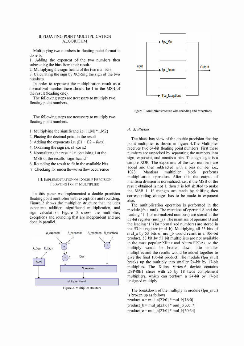
In this paper we implemented a double precision floating point multiplier with exceptions and rounding. Figure 2 shows the multiplier structure that includes exponents addition, significand multiplication, and sign calculation. Figure 3 shows the multiplier, exceptions and rounding that are independent and are done in parallel.
Multiplier Result
Figure 2. Multiplier structure
Fpu_Mul
Input Fpu_Round
Output
Fpu _Ex ce ptions
Figure 3. Multiplier structure with rounding and exceptions
A. Multiplier
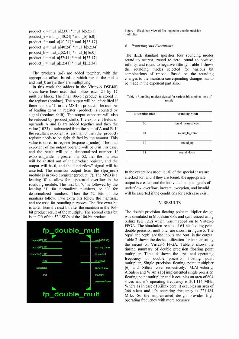
The black box view of the double precision floating point multiplier is shown in figure 4.The Multiplier receives two 64-bit floating point numbers. First these numbers are unpacked by separating the numbers into sign, exponent, and mantissa bits. The sign logic is a simple XOR. The exponents of the two numbers are added and then subtracted with a bias number i.e., 1023. Mantissa multiplier block performs multiplication operation. After this the output of mantissa division is normalized, i.e., if the MSB of the result obtained is not I, then it is left shifted to make the MSB I. If changes are made by shifting then corresponding changes has to be made in exponent also.
The multiplication operation is performed in the module (fJ:lU_mul). The mantissa of operand A and the leading 'I' (for normalized numbers) are stored in the 53-bit register (mul_ a). The mantissa of operand B and the leading' I' (for normalized numbers) are stored in the 53-bit register (mul_b). Multiplying all 53 bits of mul_ a by 53 bits of mul_ b would result in a 106-bit product. 53 bit by 53 bit multipliers are not available in the most popular Xilinx and Altera FPGAs, so the multiply would be broken down into smaller multiplies and the results would be added together to give the final 106-bit product. The module (fJ:lU_mul) breaks up the multiply into smaller 24-bit by 17-bit multiplies. The Xilinx Virtex-6 device contains DSP48E I slices with 25 by 18 twos complement multipliers, which can perform a 24-bit by 17-bit unsigned multiply.
The breakdown of the multiply in module (fJ:lU_mul) is broken up as follows product_a = mul_a[23:0] * mul_b[16:0]
product_b = mul_a[23:0] * mul_b[33:17]
product_c = mul_a[23:0] * mul_b[50:34]
product_d = mul_a[23:0] * mutb[52:51]
product_e = mul_a[40:24] * mul_b[16:0]
productj= mul_a[40:24] * mutb[33:17]
product_g = mul_a[40:24] * mul_b[52:34]
product_h = mul_a[52:41] * mul_b[16:0]
product_i =mul_a[52:41] * mul_b[33:17]
productj =mul_a[52:41] * mul_b[52:34]
The products (a-j) are added together, with the appropriate offsets based on which part of the mul_ a and mul_b arrays they are multiplying.
In this work the adders in the Virtex-6 DSP48E slices have been used that follow each 24 by 17 multiply block. The final 106-bit product is stored in the register (product). The output will be left-shifted if there is not a 'I' in the MSB of product. The number of leading zeros in register (product) is counted by signal (product_shift). The output exponent will also be reduced by (product_shift). The exponent fields of operands A and B are added together and then the value (1023) is subtracted from the sum of A and B. If the resultant exponent is less than 0, then the (product) register needs to be right shifted by the amount. This value is stored in register (exponent_under). The final exponent of the output operand will be 0 in this case, and the result will be a denormalized number. If exponent_under is greater than 52, then the mantissa will be shifted out of the product register, and the output will be 0, and the "underflow" signal will be asserted. The mantissa output from the (fJ:lU_mul) module is in 56-bit register (product_7). The MSB is a leading '0' to allow for a potential overflow in the rounding module. The first bit '0' is followed by the leading 'I' for normalized numbers, or '0' for denormalized numbers. Then the 52 bits of the mantissa follow. Two extra bits follow the mantissa, and are used for rounding purposes. The first extra bit is taken from the next bit after the mantissa in the 106-bit product result of the multiply. The second extra bit is an OR of the 52 LSB's of the 106-bit product.
Figure 4. Black box view of floating point double precision multiplier
B. Rounding and Exceptions
The IEEE standard specifies four rounding modes round to nearest, round to zero, round to positive infinity, and round to negative infmity. Table 1 shows the rounding modes selected for various bit combinations of rmode. Based on the rounding changes to the mantissa corresponding changes has to be made in the exponent part also.
Table!: Rounding modes selected for various bit combinations of rmode
Bit combination
00
01
10
\I
Rounding Mode
round nearest even - -
round to zero
round_up
round down
In the exceptions module, all of the special cases are
checked for, and if they are found, the appropriate
output is created, and the individual output signals of
underflow, overflow, inexact, exception, and invalid will be asserted if the conditions for each case exist.
IV. RESULTS
The double precision floating point multiplier design was simulated in Modelsim 6.6c and synthesized using Xilinx ISE 12.2i which was mapped on to Virtex-6 FPGA. The simulation results of 64-bit floating point double precision multiplier are shown in figure 5. The
'opa' and 'opb' are the inputs and 'out' is the output. Table 2 shows the device utilization for implementing the circuit on Virtex-6 FPGA. Table 3 shows the timing summary of double precision floating point multiplier. Table 4 shows the area and operating frequency of double preCISIOn floating point multiplier, Single precision floating point multiplier [6] and Xilinx core respectively. M.AI-AshrafY, A.Salem and W.Anis [6] implemented single precision floating point multiplier and it occupies an area of 604 slices and it's operating frequency is 301.114 MHz. Where as in case of XiI in x core, it occupies an area of 266 slices and it's operating frequency is 221.484 MHz. So the implemented design provides high operating frequency with more accuracy
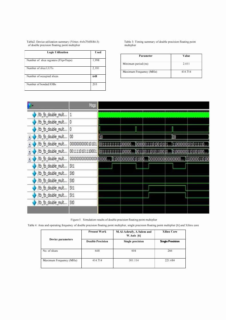
Table2: Device utilization summary (Virtex -6vlx75ttl484-3) of double precision floating point multiplier
Logic Utilization Used
Number of slice registers (Flip-Flops) 1,998
Number of slice LUTs 2,181
Number of occupied slices 648
Number of bonded lOBs 203
Table 3: Timing summary of double precision floating point multiplier
Parameter Valne
Minimum period (ns) 2All
Maximum Frequency (MHz) 414.714
Figure 5. Simulation results of double precision floating point multiplier
Table 4: Area and operating frequency of double precision floating point multiplier, single precision floating point multiplier [6] and Xilinx core
Present Work M.AI-Ashrafy, A.Salem and Xilinx Core
W.Anis l6J
Device parameters Double Precision Single precision Single Precision
No. of slices 648 604 266
Maximum Frequency (MHz) 414.714 301.114 221.484
V. CONCLUSION
The double precision floating point multiplier supports the LEEE-754 binary interchange format, targeted on a Xilinx Virtex-6 xc6vlx75t-3ff484 FPGA. The design achieved the operating frequency of 414.714 MFLOPs with area of 648 slices. The implemented design is verified with single precision floating point multiplier [6] and Xilinx core, it provides high speed and supports double precision, which gives more accuracy compared to single precession. This design handles the overflow, underflow, and truncation rounding mode
REFERENCES
[1] B. Fagin and C. Renard, "Field Programmable Gate Arrays
and Floating Point Arithmetic," IEEE Transactions on VLS1, vol. 2, no. 3, pp. 365-367, 1994.
[2] N. Shirazi, A. Walters, and P. Athanas, "Quantitative
Analysis of Floating Point Arithmetic on FPGA Based Custom Computing Machines," Proceedings of the IEEE Symposium on FPGAs for Custom Computing Machines
(FCCM"95), pp.155-162, 1995.
[3] L. Louca, T. A. Cook, and W. H. Johnson, "Implementation of IEEE Single Precision Floating Point Addition and
Multiplication on FPGAs," Proceedings of 83rd IEEE
Symposium on FPGAs for Custom Computing Machines (FCCM"96), pp. 107-116,1996.
[4] A. Jaenicke and W. Luk, "Parameterized Floating-Point Arithmetic on FPGAs", Proc. of IEEE lCASSP, 2001, vol. 2, pp. 897-900.
[5] B. Lee and N. Burgess, "Parameterisable Floating-point
Operations on FPG A," Conference Record of the Thirty
Sixth Asilomar Conference on Signals, Systems, and
Computers, 2002.
[6] Mohamed AI-Ashraf)', Ashraf Salem, Wagdy Anis., "An
Efficient Implementation of Floating Point Multiplier ", Saudi
International Electronics, Communications and Photonics
Conference (SIECPC), pp. 1-5,24-26 April 2011.
Addanki Purna Ramesh has more than 14 years of experience in teaching. He is presently working as Associate professor of Electronics and Communication Engineering at Sri Vasavi Engineering College, Tadepalligudem. He is Life Member of MIETE, Associate Member in Institute of Engineers (India).
A. V. N Tilak has more than 25 years of teaching and research experience. He obtained his Master's degree from Indian Institute of Technology, Kanpur and Ph.D. from Indian Institute of Technology, Madras during 1984 and 1997 respectively. He is presently working as a professor of Electronics and Communication Engineering at
V.R.Siddartha Engineering College, Vijayawada. He is Member of IEEE, Fellow of Institution of Electronics and Communication Engineers (TETE), Fellow of Institute of Engineers (India). He is also life member of Indian Society for Technical Education (ISTE).
Dr. A. MaIIikarjuna Prasad has more than 22 years of experience in teaching. He is presently working as a
professor of Electronics and Communication Engineering at JNTUK, Kakinada. He is Life Member of ISTE, TETE, lSI, and Society of EMC. He won best teacher award by student evaluation of 2008 batch outgoing students. He has guided about 40 students in M.Tech Instrumentation Engineering and presently guiding 8 research students for their PhD works. His areas of interest are Antennas and Process control Instrumentation. He has 25 publications in
various International and National Journals and conferences. He has conducted a "National Workshop on Electromagnetic field applications" in the year 2004.