Embed Size (px)
DESCRIPTION
Res earch Ar ticleAn Improved Fuzzy Logic Controller Design f or PV InvertersU t i l i z i n g Di f f e r e n t i a l Se a r c h O p t i m i z a t i o n
Citation preview
Research ArticleAn Improved Fuzzy Logic Controller Design for PV InvertersUtilizing Differential Search Optimization
Ammar Hussein Mutlag,1,2 Hussain Shareef,1 Azah Mohamed,1
M. A. Hannan,1 and Jamal Abd Ali1
1 Department of Electrical, Electronic and Systems Engineering, Faculty of Engineering and Built Environment,Universiti Kebangsaan Malaysia, 43600 Bnagi, Selangor, Malaysia
2 College of Electrical and Electronic Techniques, Foundation of Technical Education, Baghdad, Iraq
Correspondence should be addressed to Ammar Hussein Mutlag; ammar [email protected]
Received 15 July 2014; Revised 9 September 2014; Accepted 16 September 2014; Published 22 October 2014
Academic Editor: Pramod H. Borse
Copyright © 2014 Ammar Hussein Mutlag et al.This is an open access article distributed under the Creative Commons AttributionLicense, which permits unrestricted use, distribution, and reproduction in anymedium, provided the originalwork is properly cited.
This paper presents an adaptive fuzzy logic controller (FLC) design technique for photovoltaic (PV) inverters using differentialsearch algorithm (DSA). This technique avoids the exhaustive traditional trial and error procedure in obtaining membershipfunctions (MFs) used in conventional FLCs.This technique is implemented during the inverter design phase by generating adaptiveMFs based on the evaluation results of the objective function formulated by the DSA. In this work, the mean square error (MSE) ofthe inverter output voltage is used as an objective function. The DSA optimizes the MFs such that the inverter provides the lowestMSE for output voltage and improves the performance of the PV inverter output in terms of amplitude and frequency. The designprocedure and accuracy of the optimum FLC are illustrated and investigated using simulations conducted for a 3 kW three-phaseinverter in aMATLAB/Simulink environment. Results show that the proposed controller can successfully obtain the desired outputwhen different linear and nonlinear loads are connected to the system. Furthermore, the inverter has reasonably low steady stateerror and fast response to reference variation.
1. Introduction
The increasing global need for renewable energy has becomethe main impetus of the energy sector, primarily becauseof the negative impact of fossil fuels on the environment[1]. Photovoltaic (PV) power generation is one of the mostpromising renewable energy technologies that can be utilizedin industrial power systems and rural electrification [2].However, PV generators can only produce DC power. Thus,an electronic interface system known as a power inverteris required to link the PV generator and AC loads [3]. Inthe context of a standalone PV generator, the power inverterprovides clean and high quality power to the connectedloads. The output voltage and current waveforms under thestandalone mode of operation of the inverter should becontrolled based on the reference values. Thus, a voltagesource inverter (VSI) and an appropriate voltage controltechnique are required [4]. The main feature of a goodpower inverter is its ability to provide constant amplitude
sinusoidal voltage and frequency regardless of the type ofload it is connected to. The power inverter must also havethe capability to quickly recover from transients causedby external disturbances without causing power qualityproblems. However, the large-scale use of PV generatorsraises many challenges, such as harmonic pollutions, lowefficiency of energy conversion, fluctuation of output power,and reliability of power electronic converters [5].
Various inverter control techniques have been suggestedby many researchers to solve these problems. The propor-tional integral (PI) controller is a widely accepted techniquein inverter controls. Selvaraj and Rahim implemented adigital PI current control algorithm in a PV inverter usingDSP TMS320F2812 to keep the current injected into the gridsinusoidal. However, this PI controller requires trapezoidalsum approximation to transform the integral term into thediscrete-time domain [6]. Similarly, Sanchis et al. proposeda traditional PI controller to control a DC-to-AC boostconverter. However, their controller requires the differential
Hindawi Publishing CorporationInternational Journal of PhotoenergyVolume 2014, Article ID 469313, 14 pageshttp://dx.doi.org/10.1155/2014/469313
1
2 International Journal of Photoenergy
equations of the system to obtain good performance [7]. Ina related work, PI controllers were implemented for a three-phase inverter utilizing the dSPACEDS1104 control hardware[8]. However, themethod of tuning the gains of PI controllershas not been elaborated. Recently, researchers have focusedon the utilization of optimization techniques in PI controllertuning to achieve improved performance. An optimal DCbus voltage regulation strategy with PI controllers for agrid-connected PV system was suggested in [9]. In thiswork, the PI control parameters were optimized using thesimplex optimization technique. Other various optimizationmethods, such as particle swarm optimization (PSO), havealso been used in PI controller parameter tuning for differentapplications [10–13]. The performance of the PI controlleris limited to small load disturbances, its design is based ona precise mathematical model of the actual system underconsideration, and it requires proper tuning of its controlparameters.
Artificial intelligence- (AI-) based controllers have beenused in inverters with high efficiency and great dynamics.Various methods, such as artificial neural network (ANN),fuzzy logic, and adaptive neurofuzzy inference system-(ANFIS-) based controllers, have been reported in the litera-ture.
ANN-based maximum power point tracking controllerin a PV inverter power conditioning unit was proposed in[14]. In this work, the ANNmodule was used to estimate thevoltages and currents corresponding to a maximum powerdelivered by PV panels. The module was then utilized toobtain the desirable duty cycle of the converter. Nonetheless,this proposed controller requires large training data before itcan be trained and implemented in the controller.
Fuzzy logic controllers (FLCs) have become increasinglypopular in designing inverter controls because of theirsimplicity and adaptability to complex systems without amathematical model. Some of the good examples of FLCs forinverter control can be found in [15, 16]. In these studies, twoindividual FLCs were used to control both the DC-DC andDC-AC converters in a fuel cell grid-connected inverter andstandalone PV inverter, respectively.The authors claimed thatacceptable results can be achieved with seven membershipfunctions (MFs) and that the proposed technique can beeasily implemented. Nonetheless, the performance of FLCsdepends on the rule basis, number of rules, and MFs. Thesevariables are determined by a trial and error procedure, whichis time consuming [17].
Therefore, to overcome these limitations in FLC design,various techniques, such as ANFIS and other optimizationtechniques, have been proposed in the literature. In [17],Altin and Sefa designed a dSPACE-based grid interactiveVSI using ANFIS-based controllers. This inverter uses anANN to estimate MFs and the rule base of the controller.However, ANFIS-based methods also require training datasimilar to ANN controllers. Training data are difficult toobtain in many cases. Thus, the implementation of a particleswarm optimization (PSO) algorithmwas suggested in [18] tooptimize a nine-rule FLC formaximumpower point trackingin a grid-connected PV inverter. However, the selection of aproper optimization technique is important because PSO is
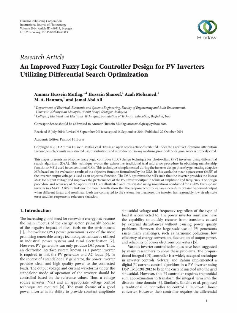
Controller
Loads
PV Converter Inverter Filter
VaVb
Vc
G1 G6
Figure 1: Structure circuit of the three-phase inverter system.
prone to premature convergence. Furthermore, such adaptiveMF tuning method in an FLC for PV inverter control has notbeen applied to date.
In the current study, an FLC optimization approach forstandalone PV inverters using the differential search algo-rithm (DSA) is proposed. The DSA is a new computationalintelligence-based technique formulated to solve both singleand multimodal optimization problems. This algorithm isspecially recommended to solve multimodal problems suchas tuning the MFs of FLCs [19]. Therefore, the utilization ofthe DSA is expected to improve the performance of FLCsfor PV inverters. The DSA optimizes the MFs of a three-phase inverter with the mean square error (MSE) of outputvoltage as the objective function. The system is modeled inthe MATLAB environment to demonstrate the performanceof the proposed controller under varying load conditions anddifferent types of loads.
2. Inverter Control Concept
Inverter control is aimed at regulating the AC output voltageat a desired magnitude and frequency with low harmonicdistortion. This regulation is carried out by the controllerby implementing a proper control strategy to maintain thevoltage at a set reference. The structure of the standalone PVinverter used in this study is shown in Figure 1 to illustrate themain control loops for achieving the above control objective.This inverter consists of a DC input from the PV source, aDC-DC converter, a DC-AC inverter, and the load. This typeof inverter with a DC input source is known as a VSI.
To apply the control strategy in the inverter system, three-phase output voltages in the synchronous reference framemust be sensed at the load terminals using appropriate voltagesensors. The three-phase output voltages of the load terminal(𝑉𝑎, 𝑉𝑏, and 𝑉
𝑐) can be represented as
𝑉𝑎= 𝑉 sin𝜔𝑡,
𝑉𝑏= 𝑉 sin(𝜔𝑡 − 2
3𝜋) ,
𝑉𝑐= 𝑉 sin(𝜔𝑡 + 2
3𝜋) ,
(1)
where 𝑉 is the voltage magnitude and 𝜔 is the outputfrequency. These voltages (𝑉
𝑎, 𝑉𝑏, and 𝑉
𝑐) are then scaled
and transformed into a 𝑑-𝑞 reference frame to simplify thecalculations for controlling the three-phase inverter [20, 21].
2
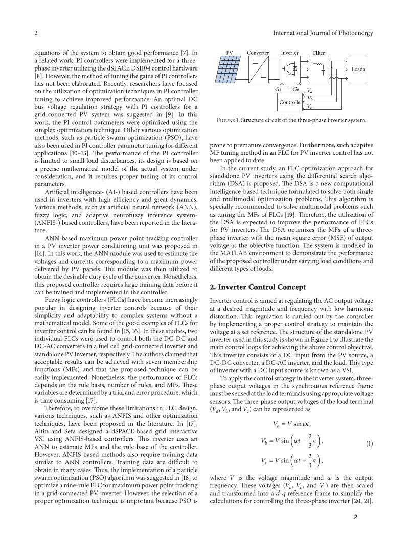
International Journal of Photoenergy 3
FLC
PLL FLC
PWM generation
CE
CE
Vabc
dqVq
Vq
Vd
Vd
Vdref
Vqref
+
+ ++
++
−
−
dq
d
dt
d
dt
E
Eabc
abc
Figure 2: Architecture of the voltage control strategy.
The two DC quantities, namely, 𝑉𝑑and 𝑉
𝑞, can be obtained
by applying Park’s transformation, as shown in (2). Thistransformation employs a 50Hz synchronization signal froma phase-locked loop block:
[
[
𝑉𝑑
𝑉𝑞
𝑉𝑜
]
]
=2
3
[[[[[[[
[
cos (𝑤𝑡) cos(𝑤𝑡 − 2𝜋
3) cos(𝑤𝑡 + 2𝜋
3)
− sin (𝑤𝑡) sin(𝑤𝑡 − 2𝜋
3) sin(𝑤𝑡 + 2𝜋
3)
1
2
1
2
1
2
]]]]]]]
]
× (
𝑉𝑎
𝑉𝑏
𝑉𝑐
) .
(2)
The error𝐸 between themeasured voltages𝑉𝑑and𝑉𝑞and ref-
erence voltages𝑉𝑑ref and𝑉𝑞ref per unit can then be computed.
Similarly, the change in error CE can be determined by takingthe derivative of 𝐸. These signals (i.e., 𝐸 and CE) are thensent to the controller at each sampling time𝑇
𝑠to compute the
missing components in𝑉𝑑and𝑉
𝑞and to generate the new𝑉
𝑑
and𝑉𝑞signals.Thenew𝑉
𝑑and𝑉𝑞are again converted into the
synchronous reference frame voltages𝑉𝑎, 𝑉𝑏, and𝑉
𝑐using the
following equation:
[
[
𝑉𝑎
𝑉𝑏
𝑉𝑐
]
]
=2
3
[[[[[[
[
cos (𝑤𝑡) − sin (𝑤𝑡) 1
cos(𝑤𝑡 − 2𝜋
3) − sin(𝑤𝑡 − 2𝜋
3) 1
cos(𝑤𝑡 + 2𝜋
3) − sin(𝑤𝑡 + 2𝜋
3) 1
]]]]]]
]
×(
𝑉𝑑
𝑉𝑞
𝑉𝑜
) .
(3)
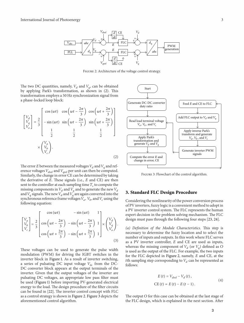
These voltages can be used to generate the pulse widthmodulation (PWM) for driving the IGBT switches in theinverter block in Figure 1. As a result of inverter switching,a series of pulsating DC input voltage 𝑉dc from the DC-DC converter block appears at the output terminals of theinverter. Given that the output voltages of the inverter arepulsating DC voltages, an appropriate low pass filter mustbe used (Figure 1) before importing PV-generated electricalenergy to the load. The design procedure of the filter circuitscan be found in [22]. The inverter control concept with FLCas a control strategy is shown in Figure 2. Figure 3 depicts theaforementioned control algorithm.
Start
duty ratio
Read load terminal voltage
Apply Park’s transformation and
Compute the error E and change in error, CE
Feed E and CE to FLC
Apply inverse Park’s transform and generate
Generate inverter PWM signals
Genereate DC-DC converter
Va, V ,b and Vc
Va, V ,b and Vc
generate Vd and Vq
Add FLC output to Vd and Vq
Figure 3: Flowchart of the control algorithm.
3. Standard FLC Design Procedure
Considering the nonlinearity of the power conversion processof PV inverters, fuzzy logic is a convenientmethod to adopt ina PV inverter control system. The FLC represents the humanexpert decision in the problem solving mechanism. The FLCdesign must pass through the following four steps [23, 24].
(a) Definition of the Module Characteristics. This step isnecessary to determine the fuzzy location and to select thenumber of inputs and outputs. In this work where FLC servesas a PV inverter controller, 𝐸 and CE are used as inputs,whereas the missing component of 𝑉
𝑑(or 𝑉𝑞) defined as 𝑂
is used as the output of the FLC. For example, the two inputsfor the FLC depicted in Figure 2, namely, 𝐸 and CE, at the𝑡th sampling step corresponding to 𝑉
𝑑can be represented as
follows:
𝐸 (𝑡) = 𝑉𝑑ref − 𝑉
𝑑(𝑡) ,
CE (𝑡) = 𝐸 (𝑡) − 𝐸 (𝑡 − 1) .
(4)
The output 𝑂 for this case can be obtained at the last stage ofthe FLC design, which is explained in the next section. After
3

4 International Journal of Photoenergy
0
0.5
1
Error (E)
Deg
ree o
f mem
bers
hip
func
tion MFE
X1 X2 X3
(a)
0
0.5
1
Change of error (CE)
Deg
ree o
f mem
bers
hip
func
tion MFCE
X4 X5 X6
(b)
Figure 4: Encoding of an MF.
the inputs and output are defined, the next stage involves thefuzzification of inputs.
(b) Fuzzifier Design. This step represents the inputs withsuitable linguistic value by decomposing every input into aset and defining a unique MF label, such as “big” or “small.”Thus, the number of MFs used in the FLC depends on thelinguistic label. The MFs of 𝐸 and CE for the FLC depictedin Figure 2 can be defined as trapezoidal and triangular MFs.This process translates the crisp values of “𝐸” and “CE” as thefuzzy set “𝑒” and “ce,” respectively, through the MF degrees𝜇𝑒(𝐸) and 𝜇ce(CE), which range from 0 to 1, as shown in
Figure 4 for triangular MFs. In Figure 4(a), the membershipfunction of error (MFE) is defined by three elements, namely,𝑋1,𝑋2, and𝑋
3, whereas the membership function of change
of error (MFCE) in Figure 4(b) is defined by another threeelements represented as𝑋
4,𝑋5, and𝑋
6.
After defining the MFs, 𝜇𝑒(𝐸) and 𝜇ce(CE) can be cal-
culated by using basic straight line equation consisting oftwo points. For example, 𝜇
𝑒(𝐸) and 𝜇ce(CE) for the MFs in
Figure 4 can be expressed, respectively, as follows:
𝜇𝑒(𝐸) =
{{{
{{{
{
𝐸 − 𝑋1
𝑋2− 𝑋1
𝑋1≤ 𝐸 < 𝑋
2
1 +𝑋2− 𝐸
𝑋3− 𝑋2
𝑋2≤ 𝐸 < 𝑋
3,
(5)
𝜇ce (CE) ={{{
{{{
{
CE − 𝑋4
𝑋5− 𝑋4
𝑋4≤ CE < 𝑋
5
1 +𝑋5− CE
𝑋6− 𝑋5
𝑋5≤ CE < 𝑋
6.
(6)
In a standard FLC design, the selection of the number ofMFs and boundary values of each MF must be adjusted bythe designer using the trial and error method until the FLCprovides a satisfactory result. However, this process is timeconsuming and laborious. After the inputs are fuzzified, thefuzzy inputs are subjected to an inference engine to generatea fuzzy output.
(c) Inference EngineDesign.This stage represents the decision-making process based on the information from a knowledge
base, which contains linguistic labels and control rules.Although there are mainly two types of inferencing systems,namely the Mamdani type and Sugeno type, the Mamdanitype inferencing system is adopted in this study due to itssimple implementation steps. The rules with two inputs forthe Mamdani type can be written as follows:
R: IF 𝐸 is “label” AND CE is “label,” THEN 𝑢 is “label.”
The quantity of rules depends on the number of inputsandMFs used in the FLC [23, 24]. An FLCwith large rule basedemands a greater computational effort in terms of memoryand computation time.
(d) Defuzzifier Design. The final step in the FLC is the selec-tion of the defuzzification method. This process generates afuzzy control action as a crisp value. Several methods can beused to generate the crisp value. The most common methodsare the center of area (COA) and the mean of maximum(MOM). The widely used COA method generates the centerof gravity of the MFs. In this study, the COA method givenin (7) is used to generate the crisp value because it is moreaccurate compared to MOMmethod [23]:
𝑂 =∑𝑛
𝑖=1𝑤𝑖⋅ 𝑢𝑖
∑𝑛
𝑖=1𝑤𝑖
, (7)
where 𝑛 is the number of rules and 𝑤𝑖is the weighted factor
that can be calculated using the Mamdani-MIN between𝜇𝑒(𝐸) and 𝜇ce(CE) as expressed in
𝑤𝑖= MIN [𝜇
𝑒(𝐸) , 𝜇ce (CE)] . (8)
The structure of each FLC depicted in Figure 2 is detailedin Figure 5. Meanwhile, the steps to implement the standardFLC are illustrated in Figure 6.
4. Proposed Optimum FLC Design Procedure
As noted in the standard FLC design procedure, the maindrawback of FLC design is the time-consuming trial anderror process used to adjust the boundary values of MFsin the fuzzification process. An improper selection of MF
4
International Journal of Photoenergy 5
FuzzifierCEE
Inference engine
Defuzzifier
Knowledge base
Z
Figure 5: FLC architecture.
Start
(5)
reach maximum rules?
using (8)
Select the inputs E and CE
Calculate the crisp value output using (7)
(6)
End
Yes
No
Rule base
Inference engine
Calculate the 𝜇e(E) using
Calculate the 𝜇ce(CE) using
i > n
i = i + 1Calculate weighted factor, wi
Calculate wi · ui
Figure 6: Encoding of the FLC.
boundaries may lead to the poor performance of the overallsystem. Therefore, this paper presents a methodology tooptimize MFs using a heuristic optimization algorithm.The heuristic optimization algorithm is used for solvingcomplex and intricate problems which are otherwise difficultto solve by classical methods. They are population basedmethods designed to solve a problem more quickly or tofind an approximate solution when classic methods fail tofind the solution especially with multimodal optimizationproblems. The differential search algorithm (DSA) has beensuggested as a heuristic optimization tool for adjusting theboundary values of MFs adaptively because of its suitabilityfor multimodal problems, such as the FLC design for PVinverter control.
4.1. Overview of Differential Search Algorithm. The DSA is anature-inspired metaheuristic optimization algorithm that is
especially effective formultimodal optimization solution [19].The concept behind its development is the seasonalmigrationof different species of nature in search of fruitful living. In theDSA, all the organisms are assumed to form a superorganismthat starts moving to discover efficient habitats. During itsmovement for discovery, the superorganism checks whethersome randomly chosen locations meet its transitory criteria.If any location is appropriate for their temporary layoversduring the journey, the individuals of the superorganism thatrevealed the stopover immediately settle in the said locationand carry on their journey from that location.
The successful migration of the superorganism dependson themechanismof the stopover site discovery.The superor-ganism tries to explore stopover sites in the area left betweenthe organisms. An exploration of the stopover sites is deter-mined using a fully random process similar to the Brownian-like random walk. Donors are made up by reshuffling allthe individuals of the superorganism and are considered tobe highly fertile in discovering the stopover site. Randomlyselected members of the superorganism move toward thetarget of donors to discover the stopover site successfully.The details of the DSA, including its basic concepts andalgorithms, can be found in [19].
4.2. Optimal FLC Problem Formulation. The three basic com-ponents that are vital to any optimization method are inputvectors, objective function formulation, and optimizationlimitations. Each component is developed and clarified toobtain optimal MFs. The optimization technique searchesthe optimal solution as formulated in the objective functionthrough manipulation of the input vector subject to theconstraints in each generation of the iterative process.
4.2.1. Input Vector. As a first step in FLC design, the numberof MFs must be defined to provide the solution from theoptimization technique. Depending on the number of MFs,the input vector 𝑍 can be expressed as
𝑍𝑖,𝑗= [𝑋1
𝑖,𝑗𝑋2
𝑖,𝑗⋅ ⋅ ⋅ 𝑋
𝑛
𝑖,𝑗] , (9)
where 𝑍𝑖,𝑗
represents the 𝑗th solution in the populationduring the 𝑖th iteration, 𝑋𝑘
𝑖,𝑗is the 𝑘th element of 𝑍
𝑖,𝑗, and
𝑛 is the total number of parameters. For example, the inputvector 𝑍
𝑖,𝑗should contain six parameters that indicate the
boundaries of MFs to be optimized to represent the MFs inFigure 4.
4.2.2. Objective Function. An objective function is requiredto determine and evaluate the performance of 𝑍
𝑖,𝑗for the
MFs. Thus, the objective function for finding the optimalvalues is formulated in such a way that 𝑍
𝑖,𝑗generates the
best fuzzy control action as a crisp value according to (7)described in the defuzzification process. In the FLC designfor PV inverter control, 𝐸 and CE at the 𝑡th sampling stepcorresponding to 𝑉
𝑑(which is the transformed inverter
output voltage) indicate the goodness of the crisp value ofthe fuzzy control action. Therefore, the mean square error
5
6 International Journal of Photoenergy
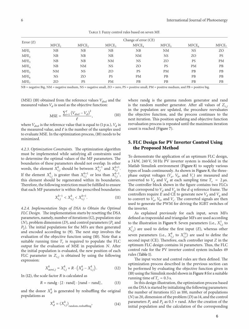
Table 1: Fuzzy control rules based on seven MF.
Error (𝐸) Change of error (CE)MFCE1 MFCE2 MFCE3 MFCE4 MFCE5 MFCE6 MFCE7
MFE1 NB NB NB NB NM NS ZOMFE2 NB NB NB NM NS ZO PSMFE3 NB NB NM NS ZO PS PMMFE4 NB NM NS ZO PS PM PBMFE5 NM NS ZO PS PM PB PBMFE6 NS ZO PS PM PB PB PBMFE7 ZO PS PM PB PB PB PBNB = negative Big, NM = negative medium, NS = negative small, ZO = zero, PS = positive small, PM = positive medium, and PB = positive big.
(MSE) (10) obtained from the reference values 𝑉𝑑ref and the
measured values 𝑉𝑑is used as the objective function:
MSE =∑ℓ
𝑖=1(𝑉𝑑ref − 𝑉
𝑑)2
ℓ, (10)
where𝑉𝑑ref is the reference value that is equal to (1 p.u.),𝑉𝑑 is
the measured value, and ℓ is the number of the samples usedto evaluateMSE. In the optimization process, (10) needs to beminimized.
4.2.3. Optimization Constraints. The optimization algorithmmust be implemented while satisfying all constraints usedto determine the optimal values of the MF parameters. Theboundaries of these parameters should not overlap. In otherwords, the element 𝑋𝑘
𝑖,𝑗should be between 𝑋
𝑘−1
𝑖,𝑗and 𝑋
𝑘+1
𝑖,𝑗.
If the element 𝑋𝑘𝑖,𝑗
is greater than 𝑋𝑘+1
𝑖,𝑗or less than 𝑋
𝑘−1
𝑖,𝑗,
this element should be regenerated within its boundaries.Therefore, the following restrictionmust be fulfilled to ensurethat each MF parameter is within the prescribed boundaries:
𝑋𝑘−1
𝑖,𝑗< 𝑋𝑘
𝑖,𝑗< 𝑋𝑘+1
𝑖,𝑗. (11)
4.2.4. Implementation Steps of DSA to Obtain the OptimalFLC Design. The implementation starts by resetting the DSAparameters, namely, number of iterations (𝐺), population size(𝑁), problem dimension (𝐷), and control parameters (𝑃
1and
𝑃2). The initial populations for the MFs are then generated
and encoded according to (9). The next step involves theevaluation of the objective function using (10). Note that asuitable running time 𝑇
𝑟is required to populate the FLC
output for the evaluation of MSE in population 𝑁. Afterthe initial population is evaluated, the new position of eachFLC parameter in 𝑍
𝑖,𝑗is obtained by using the following
expression:
𝑋𝑘
new𝑖,𝑗 = 𝑋𝑘
𝑖,𝑗+ 𝑅 ⋅ (𝑋
𝑘
𝑑− 𝑋𝑘
𝑖,𝑗) . (12)
In (12), the scale factor 𝑅 is calculated as
𝑅 = randg ⋅ [2 ⋅ rand] ⋅ [rand − rand] , (13)
and the donor 𝑋𝑘𝑑is generated by reshuffling the original
populations as
𝑋𝑘
𝑑= (𝑋𝑘
𝑖,𝑗)random reshuffling
, (14)
where randg is the gamma random generator and randis the random number generator. After all values of 𝑍
𝑖,𝑗
in the population are updated, the procedure reevaluatesthe objective function, and the process continues to thenext iteration. This position updating and objective functionreevaluation process is repeated until the maximum iterationcount is reached (Figure 7).
5. FLC Design for PV Inverter Control Usingthe Proposed Method
To demonstrate the application of an optimum FLC design,a 3 kW, 240V, 50Hz PV inverter system is modeled in theMatlab Simulink environment (Figure 8) to supply varioustypes of loads continuously. As shown in Figure 8, the three-phase output voltages (𝑉
𝑎, 𝑉𝑏, and 𝑉
𝑐) are measured and
converted to 𝑉𝑑and 𝑉
𝑞at each sampling time 𝑇
𝑠= 2 𝜇s.
The controller block shown in the figure contains two FLCsthat correspond to 𝑉
𝑑and 𝑉
𝑞in the 𝑑-𝑞 reference frame. The
controllers require 𝐸 and CE to generate new 𝑉𝑑and 𝑉
𝑞and
to convert to 𝑉𝑎, 𝑉𝑏, and 𝑉
𝑐. The converted signals are then
used to generate the PWM for driving the IGBT switches ofthe inverter.
As explained previously for each input, seven MFsdefined as trapezoidal and triangularMFs are used accordingto the illustration in Figure 9. Seven parameters (i.e., 𝑋1
𝑖,𝑗to
𝑋7
𝑖,𝑗) are used to define the first input (𝐸), whereas other
seven parameters (i.e., 𝑋8𝑖,𝑗
to 𝑋14
𝑖,𝑗) are used to define the
second input (CE). Therefore, each controller input 𝑍 in theoptimum FLC design contains 14 parameters. Thus, the FLCcontrol rule for the PV inverter control system includes 49rules (Table 1).
The input vector and control rules are then defined. Theoptimization process described in the previous section canbe performed by evaluating the objective function given in(10) using the Simulinkmodel shown in Figure 8 for a suitablerunning time of 𝑇
𝑟= 0.3 s.
In this design illustration, the optimization process basedon theDSA is started by initializing the following parameters:the number of iterations (𝐺) as 100, number of populations(𝑁) as 20, dimension of the problem (𝐷) as 14, and the controlparameters 𝑃
1and 𝑃
2as 0.3 ∗ rand. After the creation of the
initial population and the calculation of the corresponding
6

International Journal of Photoenergy 7
Start
Selection of search participants for stopover site determination
Calculate the scale factor R using (13)
Any fruitful discovery?
Update main superorganism and cost values
End
Yes
No
Yes
No
reach maximum population?
Calculate objective function, f using (10)
No
Yes
No
Yes
Output the FLC with optimal MFs parameters Z
Check the boundary for stop over site population
reach maximum iteration?
Generate initial population (Z) using (9)
reach maximum population?
Reset DSA parameters: G,N,D, i = 1, j = 1 1 and PP 2
j > N
j = j + 1 Run the system with FLC with each Zij for time Tr
Calculate objective function, f using (10)
i = i + 1
i > G
Generate target donor Xkd using (14)
Calculate the stopover site Xnewk
i,j using (12)
j = j + 1
j > N
Run the system with each FLC with Zij for time Tr
Figure 7: Proposed DSA based optimum FLC design procedure.
7

8 International Journal of Photoenergy
A
B
C
A
B
C
A
B
C
a
b
c
g
C
L
Cg g
A
B
C
E
c d
v
v
v
v
A B C
a b c
A B C
a b c
A B C
a b c
A B CA B CA B C
Ts = 2e − 06 s+
+
+
+
−
−
+−
+−
+−
−
−
Va
Vb
Vc
Vabc
Vabc
Vabc
VabVab
Iabc
Iabc
LC filter
PWMIGBT inverter
Measure
Controller
435
0.4Duty cycle
IGBT
PWM
BreakerBreaker1Breaker2
R loadRL loadNonlinear loadDiscrete,
Powergui
Figure 8: Simulation model for the three-phase inverter.
0
0.5
1
Error (E)
Deg
ree o
f mem
bers
hip
func
tion
X1i,j X2
i,j X3i,j X4
i,j X5i,j X6
i,j X7i,j
MFE1 MFE2 MFE3 MFE4 MFE5 MFE6 MFE7
(a)
0.5
0
1
Change of error (CE)
Deg
ree o
f mem
bers
hip
func
tion
X8i,j X9
i,j X10i,j X11
i,j X12i,j X13
i,j X14i,j
MFCE1 MFCE2 MFCE3 MFCE4 MFCE5 MFCE6 MFCE7
(b)
Figure 9: FLC with 7 MFs for (a) 𝐸 and (b) CE.
objective function for each input vector in the population, theDSA updates the population and initiates a new iteration. Ifthe DSA reaches the maximum iteration, the FLC with thebest MFs is obtained (Figure 7). This result indicates that theproposed approach provides a systematic and easy way todesign FLCs for PV inverter control systems. The followingsection describes the results of the optimum FLC design forthe proposed PV inverter system and its performance.
6. Results and Discussion
The PV inverter system illustrated in Figure 8 is used tovalidate the proposed DSA-based FLC (FL-DSA) optimiza-tion method and the performance of the overall system.Figure 10 shows the convergence characteristics of FL-DSA inobtaining the best optimal solution for the test system, along
with the results obtained with PSO-based FLC (FL-PSO). Fora fair comparison, both optimization methods use the samegeneral parameters, such as the number of the maximumiterations, the number of populations, and the problemdimension, as indicated in the previous section. Figure 10shows that FL-DSA converges faster than FL-PSO. Further-more, FL-DSA generates better optimal solution comparedwith FL-PSO. Note that the above optimum performanceof FL-DSA is obtained when both FLCs representing 𝑉
𝑑
and 𝑉𝑞accomplish the MFs shown in Figure 11. Considering
the effectiveness of FL-DSA, only this controller is used toevaluate the performance of the overall PV inverter systemwhen subjected to different types of loads.
6.1. Performance with Resistive Load. To evaluate the overallperformance of the proposed inverter control strategy, a
8

International Journal of Photoenergy 9
0 20 40 60 80 100Iteration
Mea
n ob
ject
ive f
unct
ion
(log)
FL-DSAFL-PSO
10−1
10−2
10−3
Figure 10: Performance comparisons based on FL-DSA and FL-PSO.
0
0.5
1
Error (E)
Deg
ree o
f mem
bers
hip
func
tion
−4 −3 −2 −1 0 1 2 3 4
MFE1 MFE2 MFE3 MFE4 MFE5 MFE6 MFE7
(a)
0 0.5 10
0.5
1
Change of error (CE)
Deg
ree o
f mem
bers
hip
func
tion
−1 −0.5
MFE1 MFE2 MFE3 MFE4 MFE5 MFE6 MFE7
(b)
0 1 20
0.2
0.4
0.6
0.8
1
Output
Deg
ree
of m
embe
rshi
p fu
nctio
n
NM NS Z PS PM PBNB
−1−2
(c)
Figure 11: MF of the (a) 𝐸, (b) CE, and (c) output.
simulation is conducted using the simulation model shownin Figure 8 for 0.1 s with a resistive load of 𝑅 = 50Ω. Inthis case, the AC output voltage waveforms of the three-phase inverter are shown in Figure 12. The waveforms aresinusoidal with 50Hz and have no negative effect, such asovershoot or oscillation. Moreover, the shift is 120∘ betweeneach phase. The controller distinctly succeeds in regulatingthemagnitude of the phase voltagewaveform at 339V and therms voltage of 240V.The controller also succeeds in following
the exact voltage reference and quickly realizing the steady-state values.
For high power capacity applications, the magnitude ofthe line voltage, such as𝑉
𝑎𝑏, is commonly considered in three-
phase systems. It is higher than the phase voltage 𝑉𝑎by a
factor of √3. The waveform of the line voltage is illustratedin Figure 13, in which the magnitude of the output waveformis 586V, whereas the rms voltage is equal to 415V as requiredby the system. Similar to the phase voltages, the line voltage is
9

10 International Journal of Photoenergy
0 0.01 0.02 0.03 0.04 0.05 0.06 0.07 0.08 0.09 0.1Time (s)
−400
−300
−200
−100
0
100
200
300
400
Volta
ge (V
)
VaVbVc
Figure 12: Output voltage waveforms (i.e., 𝑉𝑎, 𝑉𝑏, and 𝑉
𝑐) of the
three-phase inverter with 𝑅 load.
0 0.01 0.02 0.03 0.04 0.05 0.06 0.07 0.08 0.09 0.1Time (s)
0
200
400
600
Volta
ge (V
)
−600
−400
−200
Figure 13: Line voltage (𝑉𝑎𝑏) of the three-phase inverter with𝑅 load.
sinusoidal, and the controller succeeds in following the exactvoltage reference and quickly realizing the steady-state values.
The three-phase load current waveforms are also impor-tant in analysis; hence, Figure 14 is plotted. Similar to theoutput voltage waveform, the phase load current waveformshows a constant magnitude of approximately 6.8 A and anrms current of 4.8 A. This waveform is a balanced sinusoidalwaveform of 50Hz. The phase shift is also 120∘ between eachphase.
Figure 15 shows the voltage waveform and the loadcurrent waveform in which the load current waveform isscaled up by 20 times to clearly show the phase differencebetween the voltage and current waveforms. The voltage andthe current have the same phase angle and therefore followunity power factor operation as expected.
6.2. Performance with Resistive and Inductive Load. Anothertype of load is used to test the robustness of the controller. Inthis case, an 𝑅𝐿 load of 𝑅 = 50Ω, 𝐿 = 50mH is connectedto the system. The simulation is performed for 0.1 s. Thevoltage waveforms are not affected by changing the loadtype (Figure 16). The controller still succeeds in preserving
0 0.01 0.02 0.03 0.04 0.05 0.06 0.07 0.08 0.09 0.1Time (s)
0
2
4
6
8
Curr
ent (
A)
−8
−6
−4
−2
IaIbIc
Figure 14:Output currentwaveforms (i.e., 𝐼𝑎, 𝐼𝑏, and 𝐼
𝑐) of the three-
phase inverter with 𝑅 load.
0 0.01 0.02 0.03 0.04 0.05 0.06 0.07 0.08 0.09 0.1Time (s)
Volta
ge (V
), cu
rren
t (A
)
−400
−300
−200
−100
0
100
200
300
400
Va20 · Ia
Figure 15: Output voltage (𝑉𝑎) and current load (𝐼
𝑎) of the inverter
with 𝑅 load.
the magnitude of the AC output voltage waveforms for thethree-phase inverter at 339V.Thewaveforms are stable, clean,and balanced at 50Hz.
Similar to the case of resistive load, the line voltage (𝑉𝑎𝑏)
for 𝑅𝐿 load is depicted in Figure 17, wherein the amplitudeis maintained at approximately 586V, which is equivalent to415V of rms.
The three-phase load current waveforms are presentedin Figure 18 to observe the effect of 𝑅𝐿 load on the currentwaveform. The change in load does not affect the quality ofthe current waveforms.Thewaveforms are still stable, and thecontroller achieves a constant peak level with approximately6.5 A and approximately 4.5 A rms. Moreover, the waveformsare still balanced at 50Hz and displaced by 120∘ between eachphase.
10
International Journal of Photoenergy 11
0 0.01 0.02 0.03 0.04 0.05 0.06 0.07 0.08 0.09 0.1Time (s)
−400
−300
−200
−100
0
100
200
300
400
Volta
ge (V
)
VaVbVc
Figure 16: Output voltage waveforms (i.e., 𝑉𝑎, 𝑉𝑏, and 𝑉
𝑐) of the
three-phase inverter with 𝑅𝐿 load.
0 0.01 0.02 0.03 0.04 0.05 0.06 0.07 0.08 0.09 0.1Time (s)
0
200
400
600
Volta
ge (V
)
−600
−400
−200
Figure 17: Line voltage (𝑉𝑎𝑏) of the three-phase inverter with 𝑅𝐿
load.
0 0.01 0.02 0.03 0.04 0.05 0.06 0.07 0.08 0.09 0.1Time (s)
0
2
4
6
8
Curr
ent (
A)
−8
−6
−4
−2
IaIbIc
Figure 18:Output currentwaveforms (i.e., 𝐼𝑎, 𝐼𝑏, and 𝐼
𝑐) of the three-
phase inverter with 𝑅𝐿 load.
0 0.01 0.02 0.03 0.04 0.05 0.06 0.07 0.08 0.09 0.1Time (s)
Volta
ge (V
), cu
rren
t (A
)
−400
−300
−200
−100
0
100
200
300
400
Va20 · Ia
Figure 19: Output voltage (𝑉𝑎) and current load (𝐼
𝑎) of the inverter
with 𝑅𝐿 load.
0 0.01 0.02 0.03 0.04 0.05 0.06 0.07 0.08 0.09 0.1Time (s)
−400
−300
−200
−100
0
100
200
300
400Vo
ltage
(V)
VaVbVc
Figure 20: Output voltage waveforms (i.e., 𝑉𝑎, 𝑉𝑏, and 𝑉
𝑐) of the
three-phase inverter with nonlinear load.
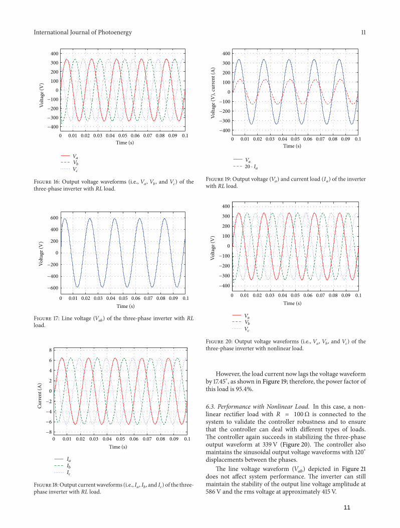
However, the load current now lags the voltage waveformby 17.45∘, as shown in Figure 19; therefore, the power factor ofthis load is 95.4%.
6.3. Performance with Nonlinear Load. In this case, a non-linear rectifier load with 𝑅 = 100Ω is connected to thesystem to validate the controller robustness and to ensurethat the controller can deal with different types of loads.The controller again succeeds in stabilizing the three-phaseoutput waveform at 339V (Figure 20). The controller alsomaintains the sinusoidal output voltage waveforms with 120∘displacements between the phases.
The line voltage waveform (𝑉𝑎𝑏) depicted in Figure 21
does not affect system performance. The inverter can stillmaintain the stability of the output line voltage amplitude at586V and the rms voltage at approximately 415V.
11

12 International Journal of Photoenergy
0 0.01 0.02 0.03 0.04 0.05 0.06 0.07 0.08 0.09 0.1Time (s)
0
200
400
600
Volta
ge (V
)
−600
−400
−200
Figure 21: Line voltage (𝑉𝑎𝑏) of the three-phase inverter with
nonlinear load.
0 0.01 0.02 0.03 0.04 0.05 0.06 0.07 0.08 0.09 0.1Time (s)
0
2
4
6
8
Curr
ent (
A)
−8
−6
−4
−2
IaIbIc
Figure 22: Output current waveforms (i.e., 𝐼𝑎, 𝐼𝑏, and 𝐼
𝑐) of the
three-phase inverter with nonlinear load.
When the nonlinear load is connected to the inverter,the load current is nonsinusoidal, as exhibited in Figure 22.However, the amplitude is stable with a peak value ofapproximately 5.9 A.
Figure 23 shows that the output currents (𝐼𝑎) have the
same phase and frequency with the output voltage (𝑉𝑎)
without any problems, such as lag, lead, and flicker. The loadcurrent waveform in Figure 23 is again scaled up to 20 timesfor a clear illustration.
In addition to the above analysis on the performance ofthe inverter with three different loads, fast Fourier transform(FFT) is performed on the inverter output waveforms toverify their quality in terms of the total harmonic distortion(THD).The quality of the waveform is inversely proportionalto the THD percentage. The THD percentage for the outputwaveforms should be less than 5% for the voltage to meet theinternational IEEE-929-2000 standard [25]. Table 2 showsthe THD percentages of the voltages and currents obtainedfor the three load types analyzed in this paper. The controller
Table 2: THD comparison.
THD Type of loadR load RL load Nonlinear load
THDV 0.56 0.54 0.91THD𝑖
0.57 1.15 30.56
Volta
ge (V
), cu
rren
t (A
)
−400
−300
−200
−100
0
100
200
300
400
0 0.01 0.02 0.03 0.04 0.05 0.06 0.07 0.08 0.09 0.1Time (s)
Va20 · Ia
Figure 23: Output voltage (𝑉𝑎) and current load (𝐼
𝑎) of the inverter
with nonlinear load.
Time (s)0 0.04 0.08 0.12 0.16 0.2 0.24 0.28
−400
−200
0
200
400
Volta
ge (V
)
VaVbVc
Figure 24: Output voltage waveforms (i.e., 𝑉𝑎, 𝑉𝑏, and 𝑉
𝑐) of the
three-phase inverter with three load types.
maintains the THD of the voltage within a very small valuefor all load types.This value is less than the 5% requirement ofthe IEEE-929-2000 standard andmore than 5% for the THDiwith nonlinear load. This result is attributed to the nonlinearnature of the current waveform drawn by the nonlinear loadthat cannot be controlled by the inverter.
6.4. Effect of Load Switching. To illustrate the performanceof the inverter during the transition from one load type toanother, we perform a simulation for 0.3 s where a resistiveload of 50Ω is connected from 0 s to 0.1 s. Then, the 𝑅𝐿
load of 𝑅 = 50Ω, 𝐿 = 50mH is connected from 0.1 sto 0.2 s. Finally, the nonlinear rectifier load with a 100Ω isconnected from 0.2 s to 0.3 s. Figure 24 illustrates the outputvoltage waveforms with different loads.The figure shows that
12

International Journal of Photoenergy 13
Time (s)0 0.04 0.08 0.12 0.16 0.2 0.24 0.28
Va
Volta
ge (V
), cu
rren
t (A
)
−400
−200
0
200
400
20 · Ia
Figure 25:Output voltage and current load of the inverterwith threeload types.
0 0.04 0.08 0.12 0.16 0.2 0.24 0.28
0200400600
Time (s)
−400−600
−200
Volta
ge (V
)
Figure 26: Line voltage (𝑉𝑎𝑏) of the three-phase inverter with three
load types.
the waveforms are sinusoidal with 50Hz and that the dis-placement between each phase is 120∘. The controller man-ages to precisely stabilize the amplitude at 339V. However,short transients occur during the transition between one loadto another, with the overshoot attributed to the switchingeffect, especially between the 𝑅𝐿 load and nonlinear load.
The voltage (𝑉𝑎) and current (𝐼
𝑎) are depicted in Figure 25
to exhibit clearly the effect of phase voltage overshootsalong with current waveform. The load current waveformis scaled up to 20 times for clarity. The voltage and currentwaveforms with 𝑅 and nonlinear load achieve unity powerfactor, whereas the voltage and current waveform with 𝑅𝐿
load achieve a power factor of 95.4%.Figure 26 illustrates the line voltage (𝑉
𝑎𝑏). Notably, the
overshoots during the transient periods are minimal whenline voltages are considered. Nevertheless, the controllermanages to regulate the amplitude at 586V. The line outputvoltage acquires a sinusoidal waveform at 50Hz.
Figure 27 shows the response of𝑉𝑑and𝑉
𝑞with three load
types in a continuous simulation run.Thefigure clearly showsa fast and good transient response. In Figure 27(a), voltage𝑉𝑑achieves the settling times in approximately 0.0013 s. In
addition, 𝑉𝑑achieves a good steady state error that keeps
the error very small. 𝑉𝑑at 0.1 and 0.2 s shows the switching
response to different loads. Figure 27(b) shows that 𝑉𝑞also
succeeds in achieving a zero value with small oscillation. Inaddition, the 𝑉
𝑞response shows that the frequency of the
waveforms is 50Hz and that the displacement between eachtwo phases is also 120∘.
0 0.05 0.1 0.15 0.2 0.25 0.3
0
0.25
0.5
0.75
1
Time (s)
ReferenceVd
Vd
(p.u
.)
(a)
0 0.05 0.1 0.15 0.2 0.25 0.3
0
0.25
0.5
Time (s)
Reference
−0.5
−0.25
Vq
(p.u
.)
Vq
(b)
Figure 27: Response of the inverter with three load types: (a)𝑉𝑑(b)
𝑉𝑞.
7. Conclusion
This paper presented an FLC-based optimization approachfor PV inverters using the DSA. First, a method was formu-lated to automatically change the MF of the FLC used in theproposed PV inverter.Thismethod is very useful in obtainingthe desired output if the MFs used can be effectively tuned byan appropriate optimization method. Second, to effectivelytune the MFs of the proposed FLC used in the PV inverter,a suitable objective function was developed to minimize theMSE of the output voltage at the inverter terminal. Finally,a relatively new optimization method known as the DSAwas proposed to tune the MFs of the FLC instead of manualtuning. The proposed method was coded and simulated inMatlab software. The FLC with seven optimally tuned MFsusing the DSA achieved good performance. The FLC for theproposed PV inverter performed excellently in tracking thereference value and regulating the output waveforms with thedesired amplitude. It also demonstrated a strong performancein terms of its quick response with minimal fluctuation fordifferent load types. A very low THD was also achieved for
13

14 International Journal of Photoenergy
the voltage with 0.56%, 0.54%, and 0.91% for the resistive,resistive inductive, and nonlinear loads, respectively.
Conflict of Interests
The authors declare that there is no conflict of interestsregarding the publication of this paper.
Acknowledgment
The authors are grateful to the Universiti KebangsaanMalaysia for supporting this research financially under GrantETP-2013-044.
References
[1] M. F. Akorede, H. Hizam, M. Z. A. Ab Kadir, I. Aris, andS. D. Buba, “Mitigating the anthropogenic global warming inthe electric power industry,” Renewable and Sustainable EnergyReviews, vol. 16, no. 5, pp. 2747–2761, 2012.
[2] A. Chel, G. N. Tiwari, and A. Chandra, “Simplified methodof sizing and life cycle cost assessment of building integratedphotovoltaic system,” Energy and Buildings, vol. 41, no. 11, pp.1172–1180, 2009.
[3] F. Blaabjerg, Z. Chen, and S. B. Kjaer, “Power electronics asefficient interface in dispersed power generation systems,” IEEETransactions on Power Electronics, vol. 19, no. 5, pp. 1184–1194,2004.
[4] R. Ortega, E. Figueres, G. Garcera, C. L. Trujillo, andD. Velasco,“Control techniques for reduction of the total harmonic distor-tion in voltage applied to a single-phase inverter with nonlinearloads: review,” Renewable and Sustainable Energy Reviews, vol.16, no. 3, pp. 1754–1761, 2012.
[5] T. Ryu, “Development of power conditioner using digitalcontrols for generating solar power,” OKI Technical Review, vol.76, no. 1, pp. 40–43, 2009.
[6] J. Selvaraj and N. A. Rahim, “Multilevel inverter for grid-connected PV system employing digital PI controller,” IEEETransactions on Industrial Electronics, vol. 56, no. 1, pp. 149–158,2009.
[7] P. Sanchis, A. Ursæa, E. Gubıa, and L. Marroyo, “Boost DC-ACinverter: a new control strategy,” IEEE Transactions on PowerElectronics, vol. 20, no. 2, pp. 343–353, 2005.
[8] M. A. Hannan, Z. Abd Ghani, and A. Mohamed, “An enhancedinverter controller for PV applications using the dSPACE plat-form,” International Journal of Photoenergy, vol. 2010, Article ID457562, 10 pages, 2010.
[9] M. Z. Daud, A. Mohamed, and M. A. Hannan, “An optimalcontrol strategy for dc bus voltage regulation in photovoltaicsystem with battery energy storage,” Scientific World Journal,vol. 2014, Article ID 271087, 16 pages, 2014.
[10] M. Liserre, A. Dell’Aquila, and F. Blaabjerg, “Genetic algorithm-based design of the active damping for an LCL-filter three-phaseactive rectifier,” IEEE Transactions on Power Electronics, vol. 19,no. 1, pp. 76–86, 2004.
[11] W. Li, Y. Man, and G. Li, “Optimal parameter design of inputfilters for general purpose inverter based on genetic algorithm,”Applied Mathematics and Computation, vol. 205, no. 2, pp. 697–705, 2008.
[12] K. Sundareswaran, K. Jayant, and T. N. Shanavas, “Inverter har-monic elimination through a colony of continuously exploring
ants,” IEEE Transactions on Industrial Electronics, vol. 54, no. 5,pp. 2558–2565, 2007.
[13] Y. A.-R. Ibrahim Mohamed and E. F. El Saadany, “Hybridvariable-structure control with evolutionary optimum-tuningalgorithm for fast grid-voltage regulation using inverter-baseddistributed generation,” IEEE Transactions on Power Electronics,vol. 23, no. 3, pp. 1334–1341, 2008.
[14] A. K. Rai, N. D. Kaushika, B. Singh, and N. Agarwal, “Simu-lation model of ANN based maximum power point trackingcontroller for solar PV system,” Solar EnergyMaterials and SolarCells, vol. 95, no. 2, pp. 773–778, 2011.
[15] A. Sakhare, A. Davari, and A. Feliachi, “Fuzzy logic control offuel cell for stand-alone and grid connection,” Journal of PowerSources, vol. 135, no. 1-2, pp. 165–176, 2004.
[16] Y. Thiagarajan, T. S. Sivakumaran, and P. Sanjeevikumar,“Design and simulation of fuzzy controller for a grid connectedstand alone PV system,” in Proceedings of the InternationalConference on Computing, Communication and Networking(ICCCN ’08), pp. 1–6, December 2008.
[17] N. Altin and I. Sefa, “DSPACE based adaptive neuro-fuzzycontroller of grid interactive inverter,” Energy Conversion andManagement, vol. 56, pp. 130–139, 2012.
[18] L. K. Letting, J. L. Munda, and Y. Hamam, “Optimization ofa fuzzy logic controller for PV grid inverter control using S-function based PSO,” Solar Energy, vol. 86, no. 6, pp. 1689–1700,2012.
[19] P. Civicioglu, “Transforming geocentric cartesian coordinatesto geodetic coordinates by using differential search algorithm,”Computers & Geosciences, vol. 46, pp. 229–247, 2012.
[20] R. Nasiri and A. Radan, “Pole-placement control strategyfor 4-leg voltage-source inverters,” in Proceedings of the 1stPower Electronic & Drive Systems & Technologies Conference(PEDSTC ’10), pp. 74–79, Tehran, Iran, February 2010.
[21] G. S. Thandi, R. Zhang, K. Xing, F. C. Lee, and D. Boroyevich,“Modeling, control and stability analysis of a PEBB based DCDPS,” IEEE Transactions on Power Delivery, vol. 14, no. 2, pp.497–505, 1999.
[22] N. Mohan, T. M. Undeland, andW. P. Robbins, Power Electron-ics: Converters, Applications, and Design, John Wiley and Sons,New York, NY, USA, 3rd edition, 2003.
[23] C.-H. Cheng, “Design of output filter for inverters using fuzzylogic,” Expert Systems with Applications, vol. 38, no. 7, pp. 8639–8647, 2011.
[24] C. Elmas, O. Deperlioglu, and H. H. Sayan, “Adaptive fuzzylogic controller for DC-DC converters,” Expert Systems withApplications, vol. 36, no. 2, pp. 1540–1548, 2009.
[25] IEEE Standard, “Recommended practices for utility interfaceof photovoltaic system,” IEEE Std 929-2000, The Institute ofElectrical and Electronics Engineers, 2002.
14