Embed Size (px)
Citation preview

AN INTEGRATED MULTICHANNEL NEURAL RECORDING SYSTEM WITH SPIKEOUTPUTS
By
YUAN LI
A DISSERTATION PRESENTED TO THE GRADUATE SCHOOLOF THE UNIVERSITY OF FLORIDA IN PARTIAL FULFILLMENT
OF THE REQUIREMENTS FOR THE DEGREE OFDOCTOR OF PHILOSOPHY
UNIVERSITY OF FLORIDA
2007
1

Copyright 2007
by
Yuan Li
2

To my family
3

ACKNOWLEDGMENTS
I would like to express my sincere gratitude to my advisor, Dr. John G. Harris, for his
support and encouragement in the past years. None of this work could be possible without
his support and guidance. Dr. Harris has always encouraged me to learn more, to think in
different perspectives and to improve myself. The expertise and wisdom he continues to
share makes me a better engineer and a better person.
I also wish to extend a gracious thank you to Dr. Jose C. Principe, who is leading the
lab and providing direction for us. I would like to thank Dr. Robert M. Fox, for all the
knowledge I learned from his courses and Dr. Justin C. Sanchez, for all the help he gave
me during my research.
Throughout my PhD research, Du Chen stands out in helping me understand
complementary metal-oxide-silicon field-effect transistors (CMOS) neural recording design.
I am very grateful for her kindness and guidance. I would like to thank Xin Qi, Dongming
Xu, Christy Rogers and Jie Xu for all of the discussions about my research. Further on, I
want to thank the rest of students in my lab; especially Jin, Xiaoxiang, Kwansun, Meena,
Dazhi, Mark and Tom, for making the lab a fun place to live and work.
I would like to express my deepest appreciation to my wife, Lin Zhang, for her great
love and support. Finally, I am especially grateful to my mother and my brother in China
for their love and support. I dedicate this dissertation to them.
4

TABLE OF CONTENTS
page
ACKNOWLEDGMENTS . . . . . . . . . . . . . . . . . . . . . . . . . . . . . . . . . 4
LIST OF TABLES . . . . . . . . . . . . . . . . . . . . . . . . . . . . . . . . . . . . . 7
LIST OF FIGURES . . . . . . . . . . . . . . . . . . . . . . . . . . . . . . . . . . . . 8
ABSTRACT . . . . . . . . . . . . . . . . . . . . . . . . . . . . . . . . . . . . . . . . 11
CHAPTER
1 INTRODUCTION . . . . . . . . . . . . . . . . . . . . . . . . . . . . . . . . . . 12
1.1 Extracellular Neural Signal Properties . . . . . . . . . . . . . . . . . . . . 121.2 Neural Recording System Overview . . . . . . . . . . . . . . . . . . . . . . 14
1.2.1 Electrodes . . . . . . . . . . . . . . . . . . . . . . . . . . . . . . . . 161.2.2 Preamplifier . . . . . . . . . . . . . . . . . . . . . . . . . . . . . . . 171.2.3 Readout Electronics and Some Data Reduction Discussion . . . . . 18
1.3 University of Florida Brain Machine Interface Project . . . . . . . . . . . . 191.4 Research Goal . . . . . . . . . . . . . . . . . . . . . . . . . . . . . . . . . . 20
2 SECOND-STAGE AMPLIFIER DESIGN . . . . . . . . . . . . . . . . . . . . . 21
2.1 Amplifier Structure . . . . . . . . . . . . . . . . . . . . . . . . . . . . . . . 212.2 Operational Transconductance Amplifier Design . . . . . . . . . . . . . . . 252.3 Noise Analysis . . . . . . . . . . . . . . . . . . . . . . . . . . . . . . . . . . 282.4 Measurement Results . . . . . . . . . . . . . . . . . . . . . . . . . . . . . . 30
3 A NOVEL TRANSCONDUCTANCE AMPLIFIER AND BIPHASICINTEGRATE-AND-FIRE NEURON . . . . . . . . . . . . . . . . . . . . . . . . 32
3.1 Introduction . . . . . . . . . . . . . . . . . . . . . . . . . . . . . . . . . . . 323.2 Transconductance Amplifier . . . . . . . . . . . . . . . . . . . . . . . . . . 343.3 Integrate-and-Fire Neuron . . . . . . . . . . . . . . . . . . . . . . . . . . . 38
3.3.1 Ideal Integrate-and-Fire Neuron and Nonidealities . . . . . . . . . . 383.3.2 Biphasic Integrate-and-Fire Neuron and Nonideality Analysis . . . . 40
3.4 Operational Transconductance Amplifier Design . . . . . . . . . . . . . . . 513.4.1 Circuit Description . . . . . . . . . . . . . . . . . . . . . . . . . . . 523.4.2 Noise and Power Consideration . . . . . . . . . . . . . . . . . . . . 53
3.5 Chip Layout . . . . . . . . . . . . . . . . . . . . . . . . . . . . . . . . . . . 553.6 Cadence Simulation Results . . . . . . . . . . . . . . . . . . . . . . . . . . 553.7 Measurement Results . . . . . . . . . . . . . . . . . . . . . . . . . . . . . . 57
3.7.1 Single-Tone Input . . . . . . . . . . . . . . . . . . . . . . . . . . . . 583.7.2 Neural-Simulator Input . . . . . . . . . . . . . . . . . . . . . . . . . 62
3.8 Practical issues . . . . . . . . . . . . . . . . . . . . . . . . . . . . . . . . . 703.8.1 Signal Dependent Reference of the Comparator . . . . . . . . . . . . 71
5

3.8.2 “Pseudo-Resistor” Introduced Direct Current Voltage Offset . . . . 73
4 EIGHT-CHANNEL BIPHASIC INTEGRATE-AND-FIRE WITH ADDRESSEVENT REPRESENTATION READOUT . . . . . . . . . . . . . . . . . . . . . 83
4.1 Introduction . . . . . . . . . . . . . . . . . . . . . . . . . . . . . . . . . . . 834.2 Address Event Representation Structure . . . . . . . . . . . . . . . . . . . 85
4.2.1 Arbiter . . . . . . . . . . . . . . . . . . . . . . . . . . . . . . . . . . 864.2.2 Row Interface . . . . . . . . . . . . . . . . . . . . . . . . . . . . . . 874.2.3 Latch and Latch Control . . . . . . . . . . . . . . . . . . . . . . . . 874.2.4 Throughput Control . . . . . . . . . . . . . . . . . . . . . . . . . . . 90
4.3 Chip Layout . . . . . . . . . . . . . . . . . . . . . . . . . . . . . . . . . . . 914.4 Measurement Results . . . . . . . . . . . . . . . . . . . . . . . . . . . . . . 92
4.4.1 One-Channel Input . . . . . . . . . . . . . . . . . . . . . . . . . . . 924.4.2 Two-Channel Input . . . . . . . . . . . . . . . . . . . . . . . . . . . 964.4.3 Three-Channel Input . . . . . . . . . . . . . . . . . . . . . . . . . . 994.4.4 Four-Channel Input . . . . . . . . . . . . . . . . . . . . . . . . . . . 1014.4.5 Eight-Channel Input . . . . . . . . . . . . . . . . . . . . . . . . . . 102
4.5 Nonideal Issues . . . . . . . . . . . . . . . . . . . . . . . . . . . . . . . . . 1054.5.1 Timing Error Forced by the Readout Clock . . . . . . . . . . . . . . 1064.5.2 Spike Delay and Spike Loss . . . . . . . . . . . . . . . . . . . . . . . 1084.5.3 Noise Issue . . . . . . . . . . . . . . . . . . . . . . . . . . . . . . . . 109
5 SINGLE-STAGE TRANSCONDUCTANCE AMPLIFIER AND BIPHASICINTEGRATE-AND-FIRE NEURON . . . . . . . . . . . . . . . . . . . . . . . . 111
5.1 Introduction . . . . . . . . . . . . . . . . . . . . . . . . . . . . . . . . . . . 1115.2 Single-Stage Transconductance Amplifier . . . . . . . . . . . . . . . . . . . 1115.3 Simulation Results . . . . . . . . . . . . . . . . . . . . . . . . . . . . . . . 116
5.3.1 Cadence Simulation . . . . . . . . . . . . . . . . . . . . . . . . . . . 1165.3.2 Matlab Simulation . . . . . . . . . . . . . . . . . . . . . . . . . . . . 118
5.4 Noise and Power Consideration . . . . . . . . . . . . . . . . . . . . . . . . 122
6 CONCLUSIONS . . . . . . . . . . . . . . . . . . . . . . . . . . . . . . . . . . . 124
REFERENCES . . . . . . . . . . . . . . . . . . . . . . . . . . . . . . . . . . . . . . . 126
BIOGRAPHICAL SKETCH . . . . . . . . . . . . . . . . . . . . . . . . . . . . . . . . 129
6

LIST OF TABLES
Table page
2-1 Characteristics of second-stage amplifier . . . . . . . . . . . . . . . . . . . . . . 30
3-1 Spike-rate comparison . . . . . . . . . . . . . . . . . . . . . . . . . . . . . . . . 65
3-2 Statistics results on the reconstructed signals . . . . . . . . . . . . . . . . . . . . 67
3-3 Statistics results on the zeroed reconstructed signals . . . . . . . . . . . . . . . . 68
3-4 Reconstructed neural signal spike sorting statistics . . . . . . . . . . . . . . . . 69
4-1 Eight-channel chip measurement summary . . . . . . . . . . . . . . . . . . . . . 106
7

LIST OF FIGURES
Figure page
1-1 Typical extracellular neuron recording techniques . . . . . . . . . . . . . . . . . 13
1-2 Typical neural recording system architecture . . . . . . . . . . . . . . . . . . . . 14
1-3 Three generations of recording system . . . . . . . . . . . . . . . . . . . . . . . 19
2-1 Schematics of second-stage amplifier . . . . . . . . . . . . . . . . . . . . . . . . 22
2-2 Resistor-feedback amplifier alternating current voltage (AC) amplituderesponse . . . . . . . . . . . . . . . . . . . . . . . . . . . . . . . . . . . . . . . . 23
2-3 Capacitor-feedback amplifier AC amplitude response . . . . . . . . . . . . . . . 24
2-4 Schematic of the Operational Transconductance Amplifier (OTA) with class ABoutput stage . . . . . . . . . . . . . . . . . . . . . . . . . . . . . . . . . . . . . . 25
2-5 AC response of the class AB OTA . . . . . . . . . . . . . . . . . . . . . . . . . . 26
2-6 Schematic of the OTA with class A output stage . . . . . . . . . . . . . . . . . . 27
2-7 AC response of the class A OTA . . . . . . . . . . . . . . . . . . . . . . . . . . 28
2-8 Measurement results from neural signal simulator . . . . . . . . . . . . . . . . . 31
3-1 Schematic of the biphasic pulse converter . . . . . . . . . . . . . . . . . . . . . . 33
3-2 Schematic of the gm amplifier . . . . . . . . . . . . . . . . . . . . . . . . . . . . 34
3-3 Equivalent circuit of the gm amplifier . . . . . . . . . . . . . . . . . . . . . . . . 35
3-4 AC response of the gm amplifier . . . . . . . . . . . . . . . . . . . . . . . . . . . 37
3-5 Ideal two-stage system for spike representation . . . . . . . . . . . . . . . . . . . 38
3-6 Schematic of the integrate-and-fire (IF) neuron . . . . . . . . . . . . . . . . . . 38
3-7 Schematic of the practical IF neuron . . . . . . . . . . . . . . . . . . . . . . . . 41
3-8 Impulse response of the gm amplifier . . . . . . . . . . . . . . . . . . . . . . . . 42
3-9 Simulated time domain results . . . . . . . . . . . . . . . . . . . . . . . . . . . . 44
3-10 Simulated time domain results . . . . . . . . . . . . . . . . . . . . . . . . . . . . 45
3-11 signal-to-noise ratio (SER) vs. sine wave frequency . . . . . . . . . . . . . . . . 49
3-12 SER vs. bypass resistance . . . . . . . . . . . . . . . . . . . . . . . . . . . . . . 51
3-13 SER vs. output resistance . . . . . . . . . . . . . . . . . . . . . . . . . . . . . . 52
8

3-14 SER vs. input capacitance . . . . . . . . . . . . . . . . . . . . . . . . . . . . . . 53
3-15 Schematic of the OTA . . . . . . . . . . . . . . . . . . . . . . . . . . . . . . . . 54
3-16 Layout of the single-channel biphasic IF neuron chip . . . . . . . . . . . . . . . 56
3-17 Reconstructed SER vs. input signal frequency . . . . . . . . . . . . . . . . . . . 57
3-18 SER vs. single tone frequency . . . . . . . . . . . . . . . . . . . . . . . . . . . . 58
3-19 Spike rate vs. sine wave frequency . . . . . . . . . . . . . . . . . . . . . . . . . . 59
3-20 Measured reconstruction time domain result example . . . . . . . . . . . . . . . 60
3-21 Threshold vs. spike rate . . . . . . . . . . . . . . . . . . . . . . . . . . . . . . . 61
3-22 Threshold vs. SER . . . . . . . . . . . . . . . . . . . . . . . . . . . . . . . . . . 62
3-23 Measured reconstruction time domain result example . . . . . . . . . . . . . . . 64
3-24 Measured reconstruction time domain result example . . . . . . . . . . . . . . . 66
3-25 Spike sorting result based on reconstructed neural signal . . . . . . . . . . . . . 68
3-26 Comparison between the correctly identified action potential (blue solid line)and the missing action potentials (red dotted lines) . . . . . . . . . . . . . . . . 70
3-27 Six action potential classes . . . . . . . . . . . . . . . . . . . . . . . . . . . . . . 71
3-28 Principal component analysis corresponding to the six templates . . . . . . . . . 72
3-29 Comparator bias current vs. SER . . . . . . . . . . . . . . . . . . . . . . . . . . 74
3-30 Equivalent circuit of gm block with DC offset . . . . . . . . . . . . . . . . . . . 75
3-31 SER vs. estimated DC offset . . . . . . . . . . . . . . . . . . . . . . . . . . . . . 77
3-32 SER vs. DC offset . . . . . . . . . . . . . . . . . . . . . . . . . . . . . . . . . . 78
3-33 SER vs. comparator threshold . . . . . . . . . . . . . . . . . . . . . . . . . . . . 80
3-34 SER vs. input single tone frequency . . . . . . . . . . . . . . . . . . . . . . . . . 81
4-1 Block diagram of the 8-channel address-event-representation (AER) recordingsystem . . . . . . . . . . . . . . . . . . . . . . . . . . . . . . . . . . . . . . . . . 84
4-2 Schematic of the arbiter cell . . . . . . . . . . . . . . . . . . . . . . . . . . . . . 86
4-3 Schematic of the row interface . . . . . . . . . . . . . . . . . . . . . . . . . . . . 87
4-4 Schematics of the latch cell and latch control . . . . . . . . . . . . . . . . . . . . 88
4-5 Schematic of the throughput control block for clocked AER . . . . . . . . . . . . 90
9

4-6 Chip layout of the 8-channel biphasic IF neuron with AER readout . . . . . . . 91
4-7 Clock frequency vs. SER (one channel) . . . . . . . . . . . . . . . . . . . . . . . 93
4-8 Clock frequency vs. output spike rate (one channel) . . . . . . . . . . . . . . . . 94
4-9 Measured reconstruction time domain result example . . . . . . . . . . . . . . . 95
4-10 Clock frequency vs. SER (two channels) . . . . . . . . . . . . . . . . . . . . . . 97
4-11 Clock frequency vs. output spike rate (two channels) . . . . . . . . . . . . . . . 98
4-12 Measured reconstruction time domain result example . . . . . . . . . . . . . . . 99
4-13 Clock frequency vs. SER (three channels) . . . . . . . . . . . . . . . . . . . . . 100
4-14 Clock frequency vs. output spike rate (three channels) . . . . . . . . . . . . . . 101
4-15 Clock frequency vs. SER (four channels) . . . . . . . . . . . . . . . . . . . . . . 102
4-16 Clock frequency vs. output spike rate (four channels) . . . . . . . . . . . . . . . 103
4-17 Clock frequency vs. SER (eight channels) . . . . . . . . . . . . . . . . . . . . . 104
4-18 Measured reconstruction time domain result example . . . . . . . . . . . . . . . 105
4-19 Clock frequency vs. SER (one channel Matlab simulation) . . . . . . . . . . . . 107
4-20 Clock frequency vs. SER (eight channel Matlab simulation) . . . . . . . . . . . 108
4-21 Channel number vs. SER (Matlab simulation) . . . . . . . . . . . . . . . . . . . 109
5-1 Schematic of single stage gm amplifier . . . . . . . . . . . . . . . . . . . . . . . 111
5-2 Equivalent circuit of the single stage gm amplifier . . . . . . . . . . . . . . . . . 113
5-3 Equivalent circuit of the single stage gm amplifier with negative input . . . . . . 113
5-4 Simulated time domain example . . . . . . . . . . . . . . . . . . . . . . . . . . . 116
5-5 Simulated time domain example . . . . . . . . . . . . . . . . . . . . . . . . . . . 117
5-6 SER vs. low frequency signal amplitude . . . . . . . . . . . . . . . . . . . . . . 119
5-7 SER vs. load capacitance . . . . . . . . . . . . . . . . . . . . . . . . . . . . . . 120
5-8 SER vs. input signal amplitude . . . . . . . . . . . . . . . . . . . . . . . . . . . 121
5-9 SER vs. input capacitance . . . . . . . . . . . . . . . . . . . . . . . . . . . . . . 122
5-10 SER vs. bypass resistance . . . . . . . . . . . . . . . . . . . . . . . . . . . . . . 123
10

Abstract of Dissertation Presented to the Graduate Schoolof the University of Florida in Partial Fulfillment of theRequirements for the Degree of Doctor of Philosophy
AN INTEGRATED MULTICHANNEL NEURAL RECORDING SYSTEM WITH SPIKEOUTPUTS
By
Yuan Li
May 2007
Chair: John G. HarrisMajor Department: Electrical and Computer Engineering
The increasing need for implantable devices in biological signal recording systems
requires compact, ultra low-power and low-noise electronics. The continuous evolution of
integrated circuit technologies partially helps in meeting these requirements by allowing
for the realization of more complex functions in a given silicon area. The shrinking power
supply helps reducing the power consumption, on the other hand, it also brings new
challenges in terms of noise.
The purpose of this research is to investigate the feasibility of a multi-channel neural
recording system with spike outputs. The multi-channel system imposes four major
constraints: large communication bandwidth, simple and compact circuit, low noise and
low power. The proposed solution is to design a novel and simple current generator which
can be directly used for biphasic spike representation. The current generator can convert
the input alternating current voltage (AC) voltage to output AC current, while eliminating
the direct current voltage (DC) voltage. By using this current generator, the total system
is more compact and less noisy. Integrating the AC current, the output of each channel
is a biphasic spike train. These multi-channel spike trains are then transmitted using the
address event representation (AER), which can improve the communication efficiency.
Preliminary theoretical analysis, simulation results and chip measurements show suitability
for neural recording applications.
11

CHAPTER 1INTRODUCTION
Scientists have long recognized the importance of the neuron as basic unit for
information processing and information storage in the human brain. Unfortunately, the
experimental methodologies to record neural electrical activity (local field potentials and
extracellular actions potentials or spikes) in freely behaving animals have become practical
only recently, and still pose many challenges. With up-to-date experimental techniques
and analytical tools, scientists have been able to extract neural information and use it
to generate real-time commands for controlling mechanical interfaces [1] or stimulating
prostheses [2], leading to the growing field of Brain-Machine Interfaces (BMI).
To better understand and utilize the mechanism in neural information processing,
scientists require many simultaneous neural recordings from behaving subjects. Thus it is
necessary to build microelectronic arrays with hundreds of electrodes and implant them
into the brain. Despite a great deal of progress during the past decades, the constraints on
power consumption, noise performance and bandwidth required to record and wirelessly
transmit the activity from a small portion of the cortex are beyond the state-of-the-art in
microelectronics and packaging. The research proposed herein addresses the IC hardware
implementation of a low-power multichannel neural recording system. In this system,
a novel voltage-to-current converter makes the biphasic spike representation practical.
The address event representation (AER) structure is used to improve the communication
channel utilization efficiency.
1.1 Extracellular Neural Signal Properties
The fluid inside of a neuron is high in potassium concentration while the outside
extracellular liquid is high in sodium concentration. The neural membrane contains
potassium, sodium and numerous other ion channels. These channels are closed in
the resting state. When a neuron receives sufficient stimuli from other neurons, its
cell membrane depolarizes and causes ionic currents to flow in its extracellular space.
Consequently, an extracellular signal is generated from the electrical charge imbalance
12

(among Na, K, Cl and other ions) on either side of the biological membrane. When
measured extracellularly, the extracellular potential raises and an action potential (also
called a spike) normally with 50–500 µV in amplitude can be observed (see Fig. 1-1).
The relevant frequencies of these action potentials range from 100Hz to about 7 KHz [3].
Normally, action potential waveforms are usually either biphasic or triphasic with pulse
widths ranging from 0.4 ms to 3 ms [4]. Action potentials generated electrochemically by
individual neurons are the commonly recorded neural signal. After the action potential
is released, the neuron needs a small amount time (typically about 1 ms) before it can
generate another spike, called the refractory period.
+
+
+
+
+
+
+
+
-
+ +
+
++
+
+
+
- + - +
+ - + -
+ - + - + - + -
+ - + - + - + - +
-
+ - + - + - + -
+ - + - + - + - +
-
+ - + - + - + -
+ - + - + - + - +
-
+ - + - + - + -
+ - + - - +
-
+ - - + - + -
+ - - + - + - +
-
+ - + - + - + -
+ - + - + - + - +
- + - + - + - + -
+ - + - + + + - +
-
+ - + - + - + -
+ - + - + - + - +
- + - + + + - + -
+ - + - + - + - +
-
+ - + - + - + -
+ - + - + - + + +
- + - + - + - + -
+ - + - + - + - +
-
- + - + -
+ - + - +
- + - + -
+ - + - +
- + - + -
+ - + - +
- + - + -
+ - + - +
+ - + - +
- + - -
+ - + - +
+
-
+
+ -
+ - +
-
+ --
+ - +
- + -
+ - +
+ -
+ - +
-
+ --
- +
+ -
+
-
+ - +
+ - + - + -
+ - + - + - +
-
+ - + - + -
+ - + - + - +
-
+ - + - + --
+
-
+
-
-
+
-
+
+
+
+
-
-
-
-
+
+
+- -
-
-
+
+-
-+
+
Neuron
[uV]
Extracellular Signal
Extracellular Fluid +
Electrode
Figure 1-1. Typical extracellular neuron recording techniques
As shown in Fig. 1-1, each electrode is surrounded by several neurons. The signals
from the closest neurons are strong and can be regarded as signals; while the signals from
farther neurons are normally attenuated too much and they can be thought as noise. One
electrode may record as many as four or five neurons. The resulting noise from distant
neurons in addition to thermal noise from electrodes can be as high as 20 µVrms. The
signal to noise ratios (SNR) therefore range from 0dB to 12dB [4]. Due to the unavoidable
electrochemical effects at the electrode-tissue interface, large DC offsets arise across the
13

recording sites. The amplitude of these DC offsets ranges from 1 V to 2 V [6], which is
much larger than the neural signals to be measured.
Besides action potentials from individual neurons, researchers are also interested in
activities of large groups of neurons. The synchronous firing of many neurons near the
electrode results in a low frequency oscillation, which is called the Local Field Potential
(LFP). The energy of the LFP in primate pre-motor and motor cortex has been shown to
correlate with specific arm reach movement parameters [7]. The frequency range of the
LFP is normally less than 100 Hz and could extend down to less than 1 Hz.
1.2 Neural Recording System Overview
From an engineering perspective, the functional building blocks of a neural recording
system are the electrodes, the pre-amplification filtering stages, and the coding and
transmission of the recorded signals. Electrodes are inserted into the tissue in the brain for
measuring the extracellular neural signal. Since the amplitude of the neural signal can be
as low as tens of µVrms, it must be amplified before further processing. Then, the boosted
signal can be transmitted away from the subject for further processing. The typical neural
recording system architecture is shown in Fig. 1-2.
Amplific atio nSig na l
Re pre se ntatio n
Transmissio n
Re c e ive rSig na l
Re c o nstruc io n
Channe l
Fro m
Ele c tro de s
To Data
Analysis
Implantab le Fro nt-End
Sig na l Pro c e ss Bac k-End
Figure 1-2. Typical neural recording system architecture
14

Most current neuronal recording systems use wires to transmit the signal from the
electrodes out of the skin. For these systems, the animal must be tethered, which restricts
the subject’s movements. The wires must be harnessed in a fashion to avoid entangling.
In addition, putting the wire through the skin can potentially cause infection at the
points where the wires break the skin for chronic implants. To get around these problems,
some research groups propose to implant the electrodes and use a wireless channel to
transmit the signal. In this case, some significant extra circuits such as oscillators,
modulators, and power amplifiers are required. Whether a wireless or wired system is
used, all the implanted parts must be as small and as lightweight as possible, especially
if multiple channels are to be recorded. In addition, some other factors also need careful
consideration.
Lower power consumption is also an important consideration to avoid damaging
surrounding tissue. Researchers have shown that a heat flux of only 80 mW/cm2 can cause
necrosis in muscle tissue [8] which severely restricts the power budget for a multiple chan-
nel neural recording system. Batteries powering the implant must be either periodically
replaced or frequently recharged.
Since the neural signals to be recorded have amplitudes of tens of microvolts with
frequency ranging from 1 Hz to 7 KHz, a low noise and low frequency band-pass filter
must be used. Considering such tiny neural signals are superimposed on much larger DC
offsets introduced by the electrodes, the system must accommodate large input offsets at
the preamplifiers, which leaves the AC coupling system a good choice.
Because most of the preamplifiers can provide an intermediate gain of around 40dB,
the output signal from the preamplifier is still small. A second stage amplifier is normally
used to further boost the signal. The final output signal can be transmitted in an analog
format or in digital format after analog-to-digital conversion.
15

1.2.1 Electrodes
The electrodes are the first stage of the neural recording system. Therefore, the
properties of the electrodes greatly impact the performance of the total system. The more
accurate the neural recordings are from the electrodes, the higher the SNR of the output
signal will be. In order to record the extracellular neural signal from a few neurons, the
electrodes must be comparable to the size of the neurons (normally 50 µm or less). The
tips of the electrodes must be sharp enough to penetrate the tissue. In addition to the
physical requirements, the electrodes must also be biologically compatible so that they can
continue to record the neural signals over extended periods of time from months to years.
There are two major classes of electrodes: passive and active. Passive electrodes
are defined as ones which do not have any electronic circuit on the electrode substrate
[9]. Three basic passive electrodes widely used by neurophysiologists are metal, glass
micropipette and photoengraved microelectrodes. Active electrodes are characterized as
ones which include electronic circuits on the same substrate as the recording electrodes.
The on-chip circuits can be used to amplify the recorded signal, and change the output
data format. The circuits can also potentially minimize the effects of leakage from the
output wires, therefore improving the accuracy of the recorded signals. The first known
attempt to fabricate an active microelectrode array was made by Wise in 1975 at the
University of Michigan [10].
To optimize the performance of the electrodes, three aspects should be carefully
considered in terms of AC frequency response, DC drift, and noise level:
1. The AC frequency response: Since the frequency of the recording signal extends frombelow 1 Hz to around 7 KHz, the electrodes must not attenuate the signal within thisfrequency band.
2. The DC shift: One of the major challenges in interfacing electronics to a recordingelectrode is the random wandering of the DC voltage. The DC potential between anelectrolyte and a metal electrode is subject to substantial variations and can be ashigh as 50 mV for a gold surface, which is around 1000 times larger than the neuralsignal to be recorded.
16

3. The noise level: It is expected that the input-referred electrode noise must besignificantly smaller than the amplitude of the measured signal. Since the amplitudeof the neural signal could be as low as 50 µV, it is important that the total inputnoise is below 20 µVrms [4]. The electrode noise results from the neural backgroundnoise and thermal noise which is related to the recording bandwidth.
1.2.2 Preamplifier
Because the neural signal to be recorded has such a low amplitude, it must be
amplified before it can be further processed. The properties of the signals also put some
restrictions on the preamplifier. The preamplifier should have very low noise, have suitable
frequency response, consume very low power, and be fully integrated. Since the frequency
range of interest ranges from below 1 Hz to around 7 KHz, the preamplifier must reject
high frequency signals to improve the SNR. Considering the large DC shift associated with
the electrodes, the amplifier should also be able to reject the DC signal while passing the
AC signal. The noise performance of the preamplifier is also very important, because the
noise introduced in this stage will be carried and amplified by the following amplifier.
To achieve a very low cutoff frequency, a large time constant is required, which means
either a large capacitor, a large resistor or both. Some instrumentation amplifiers utilize
external capacitors in the range of nano Farads to create a low enough cut-off frequency
[4]. Such large capacitors are impractical for fully-integrated applications with current
technology. When a multichannel recording system is considered, this problem becomes
even more severe.
Based on Harrison’s design [6], Chen and Harris from the University of Florida
have used diode-connected PMOS transistors acting as “pseudo-resistors” to develop a
low-power low-noise fully integrated neural amplifier (bioamplifier) [11]. The “pseudo-
resistor” has huge resistance (greater than 100GΩ) while occupying a very small area.
This property makes it practical to fully integrate an amplifier with a very low cutoff
frequency.
17

1.2.3 Readout Electronics and Some Data Reduction Discussion
The amplified signal needs to be transferred for further signal processing. The simple
and straightforward readout method is to directly transmit the amplified analog signal
[4, 12]. For multichannel neural recording systems, the number of output leads will
increase as the number of recording channels increases. An analog multiplexer can be used
to reduce the output leads [13]. The amplified analog signal can also be digitized and then
transmitted.
For more advanced systems, the data and power transfer between the implant unit
and the outside world can be achieved through a wireless channel. Recorded signals could
be digitized before transmission which requires an on-chip ADC to enhance the signal-
to-noise ratio (SNR). To reduce the data rate, limited on-chip digital processing such
as compression [14] and spike detection can be used. On the other hand, the ADC and
modulators increase the die area and power consumption of the system.
Compared to analog, digital signals are much more robust to transmit, are easy
to store and can be processed by powerful digital algorithms. However, a conventional
ADC using Nyquist periodic sampling is not a suitable choice due to its large power
consumption when increasing the resolution. One solution to this limit is to employ the
integrate-and-fire (IF) representation [11, 15]. Single-direction spike representation has
been proven to reduce the required transmission data while still keeping the signal fidelity
[11, 15]. However, to generate unidirectional IF spikes, the existing single-direction spike
generator has to shift the current to guarantee only positive outputs. The resulting prob-
lem is the shifting DC increases the overall firing rate and thus wastes communication
bandwidth, and also wastes power. To solve this problem, the biphasic spike representa-
tion was developed for further data reduction [5].
Another choice to compress the transmission data is to just transmit the exact timing
of each action potential, which is associated with the spike detection technique. Even
though there is a debate about whether the neural information is encoded in the rate
18

of the spikes or with individual timing, both sides agree that the recording of the exact
timing of the spikes is crucial for further data analysis. However, for extracellular neural
recording systems, multiple neurons are recorded on the same electrode, and in this case a
simple spike timing is not enough to distinguish among these neurons. Spike sorting can
be used to tag each spike before the transmission [16]. The detailed information about
spike detection and spike sorting can be found in [16].
1.3 University of Florida Brain Machine Interface Project
The University of Florida BMI project is one part of a multi-university DARPA-
sponsored project. The final target is to develop a new generation of tools in which direct
brain machine interfaces (BMIs) are used to allow subjects to interact seamlessly with a
variety of actuators and sensory devices through the expression of their voluntary brain
activity [17].
2nd-stageamplifier
2nd-stagegm amplifier
Generation
1Generation2
CommercialADC
PICOsystem
ModulatorAER
multiplex
Generation
3
1st-stagegm amplifier
Modulator
Preamplifier(D. Chen)
AERmultiplex
Biphasic IF(D. Chen)
Preamplifier(D. Chen)
Biphasic IF(D. Chen)
Figure 1-3. Three generations of recording system
Fig. 1-3 shows the three generations of hardware recording system proposed in the
UF BMI project. In the first generation, the neural signal will be directly amplified by
80dB and the analog output will be sampled with a commercial product. In the second
generation, the differential neural signal will be first amplified by 40dB. The boosted
signal will then be encoded by a biphasic IF neuron. When there are more than one
channel in this system, an AER readout circuit is needed to multiplex these channels. The
third generation removes the preamplifier used in the second generation. When necessary,
19

the final outputs from any of the three generations can be transferred with either wireless
or wired channels.
1.4 Research Goal
The goal of this research is to develop a multichannel neural recording system.
The organization of this dissertation is as follows: Chapter 2 introduces a second-stage
amplifier design, which can be cascaded to the preamplifier to provide an 80dB gain for
the following ADC process (the second block in generation 1 in Fig. 1-3). In Chapter
3, a novel voltage-to-current converter is presented (the second block in generation 2 in
Fig. 1-3). This current generator makes the biphasic spike representation practical. The
simulation results when used as the second stage are presented there with some system
analysis. Some chip measurement results including the single tone and neural simulator
signal will also be given. Chapter 4 combines the widely used address event representation
(AER) to the spike representation (the fourth block in generation 2 in Fig. 1-3), and a
8-channel biphasic IF AER system is proposed. This system transfers 8 channel biphasic
IF outputs with 4 readout leads and thus greatly improves the communication channel
efficiency. Some simulation and chip measurement results will be shown in this chapter.
The biphasic spike representation discussed in chapter 2 has to be used in the second
stage, where the first stage converts the differential neural signal into single-ended signal
and boosts the signal level. To simplify the circuit design, the single stage biphasic spike
circuit is proposed. The Cadence simulation and circuit analysis will be given in chapter
5 (the first block in generation 3 in Fig. 1-3). At last, the conclusions are discussed in
Chapter 6.
20

CHAPTER 2SECOND-STAGE AMPLIFIER DESIGN
A low-noise 40dB bio-preamplifier was designed and tested as part of the University of
Florida BMI project [11]. However, considering the typical neural signals have amplitudes
of 50–500µV [3], the output from the preamplifier has amplitude of 5–50 mV, which is still
too small for input to commercial ADCs. Therefore, a second-stage amplifier is designed to
further amplify the signal.
2.1 Amplifier Structure
The second-stage amplifier has been implemented in two different structures. One of
the structures was originally proposed by Harrison in [6] and later used by Chen in the
preamplifier [11], which uses a capacitor-feedback network. Another version consists of a
resistor-feedback network. Fig. 2-1 shows the schematic of each amplifier. Both structures
operate with a ±2.5V power supply.
In the resistor-feedback amplifier, R1 and C1 consist of a high-pass filter, which can
remove the DC component of the output signal from the preamplifier. Without this high-
pass filter, the output DC offset from the preamplifier can easily drive the second-stage
amplifier into the saturation region. The midband gain is determined by the ratio of the
two resistors R3/R2. This amplifier circuit was fabricated in the AMI 0.6µ three-metal
two-poly process with a designed gain of 40dB. Using poly resistors, R1 was set to 9.4MΩ,
R2 to 14.29KΩ and R3 to 1.429MΩ (all these value were extracted in Cadence from the
layout). C1 was set to 180pF using poly-to-poly capacitors. C2 was used to simulate
the external capacitor load (including the package and the probe) and was set to 16pF.
This capacitor was not inside the chip layout. Since the extracellular action potentials
range from approximately 100Hz to 7KHz in the frequency domain [3], C1 and R1 need to
provide a cutoff frequency lower than 100Hz. The chosen values set the cutoff frequency at
94Hz.
The simulated frequency response using Cadence spectreS is given in Fig. 2-2. The
amplifier was designed to have a low cutoff frequency of 94Hz and high cutoff frequency
21

OTA
C1
R1
R2 R3
Vout+
-
Vin
C2
(a)
Vin
Vref
OTA
+
-
Vout
M2M1
C1
C2
C3
(b)
Figure 2-1. Schematics of second-stage amplifier: (a) Resistor-feedback network; (b)Capacitor-feedback network (the real circuit has 6 diode-connected transis-tors).
of 19KHz, with the midband gain of 40dB. Since the preamplifier has cutoff frequencies
of 0.3Hz and 5.4KHz [5], the high cutoff frequency of the second-stage amplifier will not
have much effect on the final output signal. The 94Hz-low-cutoff-frequency will remove
the Local Field Potential (LFP) signal from the preamplifier output signal. This is one
of the disadvantages of this structure, however most neuron researchers ignore the LFP
anyway. In this resistor-feedback structure, on-chip resistors and capacitors require such
huge resistance and capacitance that they take up too much chip area. In fact, the resistor
and capacitor together use more than 90 percent of the layout area in the test chip. This
is the major disadvantages of this structure. Another disadvantage is that the resistors
continuously consume power, which is very serious since the valuable layout area prevents
22

us from further increasing the resistance. The power consumed by the resistor is inversely
proportional to R3, and proportional to the mean square of the output voltage. Such
power waste must be avoided in low-power applications. In addition, the input DC offset
of the operational transconductance amplifier (OTA) plays an important role here. When
there is no DC offset, the output DC voltage equals the reference voltage. However, if
Voff 6= 0, then Vout − Vref = 100× Voff , which will possibly push the OTA out of its linear
region. Therefore, care must be taken in circuit design and chip layout to reduce the input
DC offset. In terms of the circuit design, the mismatch of the input differential pair has
the largest contribution to the offset voltage. Increasing the areas of these transistors can
reduce the DC offset with the added risk of degrading the OTA’s stability. A common-
centroid layout was used to reduce transistor mismatch.
100
101
102
103
104
105
106
0
10
20
30
40
50
Frequency (Hz)
Gai
n (d
B)
AC response
Figure 2-2. Resistor-feedback amplifier alternating current voltage (AC) amplitude re-sponse
The capacitor-feedback amplifier was designed to avoid the above disadvantages in
the resistor-feedback amplifier. In this structure, the capacitor ratio C1/C3 determines
the midband gain, while Vref and 6 diode-connected transistors together provides the
DC operation bias. It was claimed that when the voltage difference across a single diode-
connected transistor is less than 0.2V, the diode-connected transistor can be viewed as a
“pseudo-resistor” with a resistance larger than 1011Ω [11]. Since most action potentials
23
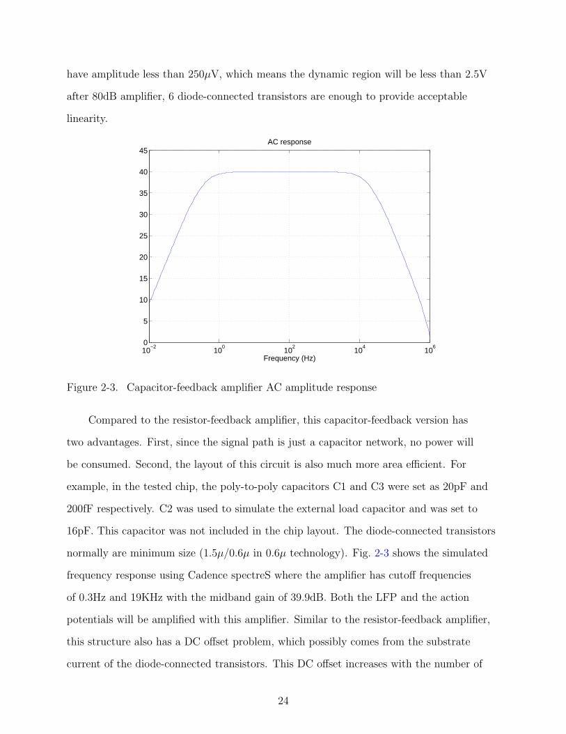
have amplitude less than 250µV, which means the dynamic region will be less than 2.5V
after 80dB amplifier, 6 diode-connected transistors are enough to provide acceptable
linearity.
10−2
100
102
104
106
0
5
10
15
20
25
30
35
40
45
Frequency (Hz)
AC response
Figure 2-3. Capacitor-feedback amplifier AC amplitude response
Compared to the resistor-feedback amplifier, this capacitor-feedback version has
two advantages. First, since the signal path is just a capacitor network, no power will
be consumed. Second, the layout of this circuit is also much more area efficient. For
example, in the tested chip, the poly-to-poly capacitors C1 and C3 were set as 20pF and
200fF respectively. C2 was used to simulate the external load capacitor and was set to
16pF. This capacitor was not included in the chip layout. The diode-connected transistors
normally are minimum size (1.5µ/0.6µ in 0.6µ technology). Fig. 2-3 shows the simulated
frequency response using Cadence spectreS where the amplifier has cutoff frequencies
of 0.3Hz and 19KHz with the midband gain of 39.9dB. Both the LFP and the action
potentials will be amplified with this amplifier. Similar to the resistor-feedback amplifier,
this structure also has a DC offset problem, which possibly comes from the substrate
current of the diode-connected transistors. This DC offset increases with the number of
24

the diode-connected transistors. Fortunately, the measurement results indicate that the
DC offset with 6 “pseudo-resistors” is always less than 500mV, which will not affect the
OTA’s linear operation very much. If necessary, Vref can be used to adjust the output DC
offset.
2.2 Operational Transconductance Amplifier Design
Vout1 Vout
C1
VDD
Vin+ Vin-
M1 M2
M3 M4M5 M6
M7 M8
M9 M10
M11 M12
M13
M14
M16
M15
M18
M17
Ibias
VSS
VDD
Figure 2-4. Schematic of the Operational Transconductance Amplifier (OTA) with classAB output stage
Fig. 2-4 shows the first design of the OTA used in the 40dB second-stage amplifiers.
This is a typical two stage OTA. The first stage is a P-type input differential pair loaded
with Wilson current mirrors. A cascode current mirror is used to convert the differential
output into a single-ended output. Due to the high output impedance of the cascode
current mirror and the Wilson current mirror, the first stage provides a large gain:
A = GmRout (2–1)
where Gm is the transconductance of differential input pair, and Rout is the cascode
current mirror output resistance parallel connected with the Wilson current mirror output
25

resistance:
Rout ' gm10ro10ro12‖gm8ro8ro6 (2–2)
The second stage is a voltage follower followed by a simple class-AB output
stage. M13 and M16 are DC voltage shifters while M17 and M18 form a push-pull
common-source output stage. This second stage also provides intermediate signal gain,
gm17(ro17‖RL) or gm18(ro18‖RL), depending on which transistor is active. The voltage
shifter controls the quiescent current of the output stage and the class-AB output stage
can sink or source more current when necessary. In addition, this common-source output
stage provides a rail-to-rail output range, which is expected in this 40dB second-stage am-
plifier. The Cadence simulation shows that the output DC voltage ranges from VSS+0.4V
to VDD-0.4V. This DC output range is enough for most action potentials. However, when
the action potential amplitude is greater than 400 µV, there will be some distortion in
the output. Increasing the quiescent current can increase the output DC range while
consuming more power.
10−2
100
102
104
106
0
50
100
150
10−2
100
102
104
106
−200
−150
−100
−50
0
Frequency (Hz)
Figure 2-5. AC response of the class AB OTA
26
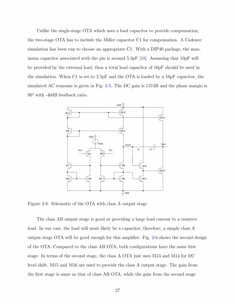
Unlike the single-stage OTA which uses a load capacitor to provide compensation,
the two-stage OTA has to include the Miller capacitor C1 for compensation. A Cadence
simulation has been run to choose an appropriate C1. With a DIP40 package, the max-
imum capacitor associated with the pin is around 5.3pF [18]. Assuming that 10pF will
be provided by the external load, then a total load capacitor of 16pF should be used in
the simulation. When C1 is set to 2.5pF and the OTA is loaded by a 16pF capacitor, the
simulated AC response is given in Fig. 2-5. The DC gain is 137dB and the phase margin is
90o with -40dB feedback ratio.
Vout1 Vout
C1
VDD
Vin+ Vin-
M1 M2
M3 M4M5 M6
M7 M8
M9 M10
M11 M12
M13
M14
M16
M15
Ibias
VSS
VDD
R
Figure 2-6. Schematic of the OTA with class A output stage
The class AB output stage is good at providing a large load current to a resistive
load. In our case, the load will most likely be a capacitor, therefore, a simple class A
output stage OTA will be good enough for this amplifier. Fig. 2-6 shows the second design
of the OTA. Compared to the class AB OTA, both configurations have the same first
stage. In terms of the second stage, the class A OTA just uses M13 and M14 for DC
level shift. M15 and M16 are used to provide the class A output stage. The gain from
the first stage is same as that of class AB OTA, while the gain from the second stage
27

10−2
100
102
104
106
0
50
100
Gai
n (d
B)
10−2
100
102
104
106
−100
−50
0
Frequency (Hz)
Pha
se (
deg)
Figure 2-7. AC response of the class A OTA
is gm16(ro16‖ro15‖RL). R and C1 are used to provide the Miller compensation and their
values have to be determined from Cadence simulation with a load capacitor. When the
load capacitor of 16pF is used in the Cadence simulator, R and C1 can be set to 175KΩ
and 2.5pF respectively to achieve around 90o phase margin for 40dB amplifier (see Fig. 2-
7). The DC gain of this class A OTA is around 126dB, which is a little bit lower than that
of class AB.
2.3 Noise Analysis
Compared to the preamplifier, the noise performance in the second-stage amplifier
is less crucial but it still needs some attention. The following analysis concentrates on
the thermal noise and the flicker noise, because they are the major noise sources in this
low-frequency CMOS application.
Both of the rail-to-rail OTAs have a two stage structure and the first stage has a
huge gain, thus the second stage has little contribution to input-referred noise and will
be neglected in the analysis. In the first stage, M7∼M10 are common gate transistors
and their noise contribution is negligible. Assuming that this circuit is perfectly matched,
28

which means that M3∼M6 (indicated by M3) have the same size, M1 and M2 (indicated
by M1) have the same size and so do M11 and M12 (indicated by M11), the input-referred
thermal noise is:
v2ni,OTA = [
16κT
3gm1
(1 + 2gm3
gm1
+gm11
gm1
)]∆f (2–3)
From Eq. 2–3, it is clear that the input-referred thermal noise can be reduced by in-
creasing gm1 or decreasing gm3 and gm11. The straightforward approach to achieve these
is to increase (W/L)1,2 or decrease (W/L)3,4,5,6, (W/L)11,12. However, the sizes and the
transconductance of M3∼M6 and M11∼M12 are related to the second and third non-
dominant poles by ωi ' gmi/Ci, where Ci is the total capacitance seen by the gate of Mi.
Reducing their sizes (reducing the gm) will push these poles close to the zero and may
introduce stability problems. Consequently, there is a tradeoff between stability and input
referred thermal noise.
Since the flicker noise is inversely proportional to the WL of the transistors, one
method to decrease the flicker noise is to increase the transistor area. However, with
the increase of the transistor area, the associated parasitic capacitors are also increased,
therefore possibly introducing the stability concerns. On the other hand, the total input-
referred noise of the capacitor-feedback amplifier is related to that of OTA by:
v2ni,amp = v2
ni,OTA(C1 + C3 + Cin
C1)2 (2–4)
where C1, C3 are shown in Fig. 2-1 and Cin is OTA input parasitic capacitor. With
increasing WL of the input transistors, Cin and also v2ni,amp will be increased. As a result,
there is a tradeoff between the amplifier input-referred flicker noise, OTA input-referred
total noise and system stability. It is also believed that PMOS devices experience less
flicker noise than NMOS devices [19] and PMOS transistors are chosen for the differential
pair for this reason.
29

Table 2-1. Characteristics of second-stage amplifier
Parameter Capacitor-feedback Amp Resistor-feedback Amp
Supply voltage 5V 5VPower consumption ∼120µW ∼120µW
Gain ∼40dB ∼40dBInput DC offset 1∼5mV 1∼5mV
Low cutoff frequencies <1Hz ∼94HzHigh cutoff frequencies ∼19KHz ∼19KHz
Layout area ∼66400µm2 ∼860000µm2
Output DC range VSS+0.45∼VDD-0.5 VSS+0.45∼VDD-0.5
2.4 Measurement Results
The amplifier with class AB OTA has been fabricated using the AMI 0.6um process
with a DIP40 package. All the capacitors were implemented with poly layers. The chip
has been successfully tested.
During all the measurement setups, the OTA was biased with 8µA current. First,
the DC characteristics were tested based on 10 resistor-feedback amplifiers. Of the 10
channels, 4 channels’ DC offset were less than 1 mV; 3 were less than 2 mV; 2 were
less than 3 mV and 1 was less than 5mV. The resulting maximum output DC offset is
less than 500mV. Apparently, such small DC offset is not a big issue in this application
considering the power supply and the signal dynamic range, which will also be verified by
the following measurement results.
An Agilent 33220A signal generator was used in the testing. The measurement results
are similar to the Cadence simulation. The gain is around 40dB, and the cutoff frequencies
also match the Cadence simulation. The minimum and maximum DC output values are
0.45V and VDD-0.5V. One of the chips includes the first 40dB amplifier designed by Chen
[11] cascaded by the resistor-feedback 40dB amplifier and this cascaded 80dB amplifier was
also tested. The signal from the Agilent 33220A was first attenuated by 40dB and then fed
into the 80dB amplifier as input and the measurement results verify the simulation. The
specifications of these two second-stage amplifiers are listed in Table 2-1.
30

The Bionic 128 Channel Neural Signal Simulator was also used for the testing. Two
setups were used in this testing. The first setup is Chen’s 40dB preamplifier and second-
stage 40dB amplifiers which were fabricated in individual chips and cascaded externally.
One of the measurement results from this setup is given in Fig. 2-8. The neural action
potentials with amplitude of around ±1.0V are clear and the total gain is around 80dB.
When these two stages were fabricated in the same chip, no matter whether the output
from the preamplifier to input of the second-stage amplifier was internally or externally
connected, there was always a steady oscillation once the input is connected to the neural
signal simulator. The oscillation frequency is around 6KHz and it can be finely adjusted
by the bias current. However, these same setups always work very well with the Agilent
33220A signal generator. We suspect that this oscillation comes from the input impedance
mismatch and the substrate power supply kick-back due to the heavy substrate doping.
−0.02 −0.015 −0.01 −0.005 0 0.005 0.01 0.015−2
0
2
−0.02 −0.015 −0.01 −0.005 0 0.005 0.01 0.015−2
0
2
−0.02 −0.015 −0.01 −0.005 0 0.005 0.01 0.015−2
0
2x 10
−4
Time (second)
Figure 2-8. Measurement results from neural signal simulator: (a) Results from thecapacitor-feedback amplifier; (b) Results from the resistor-feedback amplifier;(c) Neural signal simulator output.
31

CHAPTER 3A NOVEL TRANSCONDUCTANCE AMPLIFIER AND BIPHASIC
INTEGRATE-AND-FIRE NEURON
3.1 Introduction
Compared to analog signals, digital signals are much more robust to transmit, easily
storable and can be processed by powerful digital algorithms. The most popular A/D
converter is based on periodic Nyquist-Rate sampling, which can be loosely defined as a
converter which generates a uniformly spaced series of binary output values corresponding
to an instantaneous input value. The resolution of such an A/D converter is limited by
the power budget of the particular application. ∆ − Σ A/D converters are commonly used
to relax the requirements on the analog circuit at the expense of more complicated digital
circuitry [20].
Inspired by research results in neuroscience that suggest biological systems represent
sensory information using the timing of all-or-nothing action potentials [21], a low-power
pulse signal representation circuit has been proposed for neural recording applications
[11, 15]. This circuit converts an analog voltage waveform to a pulse train and the original
analog signal can be reconstructed with a digital algorithm under certain assumptions.
The existing pulse output circuit converts the voltage to a current that was shifted to
guarantee positive only outputs. The positive current was then fed into a simple integrate-
and-fire (IF) neruon circuit for generating a spike train. Even though this circuit has been
shown to encode the original signal with high SNR (103 dB in Matlab simulation), there
are still major improvements necessary to reduce the data rate and the overall power
consumption.
By shifting the current so that there is only positive current, the overall firing rate,
the power consumption and the required communication bandwidth have been greatly
increased. The extreme case is that when the signal during some period is zero, the shifted
signal will still generate unnecessary spikes.
32

Comparator 1
Comparator 2
Vth+-
Vin
+
Vth-+
-M1
Current x(t)
VmidVmid
Buffer OR
Positive pulse
Negative pulse
Figure 3-1. Schematic of the biphasic pulse converter
To solve this problem, a biphasic spike representation is proposed [11]. Rather
than shift the signal to be positive only, a biphasic mode spike generators using two
comparators with different thresholds is implemented in Fig. 3-1. A single capacitor is
used to integrate the input current but a positive and negative threshold are implemented
using two comparators. When the voltage across the capacitor rises above the positive
threshold, a “positive” spike is generated; similarly a “negative” pulse is created when the
voltage drops below the negative threshold. After either spike is generated, the voltage
on the capacitor is reset to a midrange voltage value by the digital control circuit. When
the input current is zero-valued, no spike will be generated; on the other hand, if the
amplitude of the input current is high, the firing rate will be correspondingly high. A
simulation for a speech signal has shown that this structure dramatically reduce the firing
rate without sacrificing the signal fidelity [5].
Even though this circuit has many advantages compared to the unidirectional pulse
representation, the circuit to generate the required current has been a problem because
this current generator must be able to reject the DC component of the signal and convert
only the AC voltage to AC current. Proper DC biasing must be set to allow the OTA
(operational transconductance amplifier) to operate in a suitable region. At the same
33
time, the output resistance should be high enough for reducing the leaky current. In this
chapter, a novel and simple current generator to generate biphasic spikes is proposed.
Matlab simulation results and chip measurements will be shown. Following these, some
nonideal factors in this circuit are discussed.
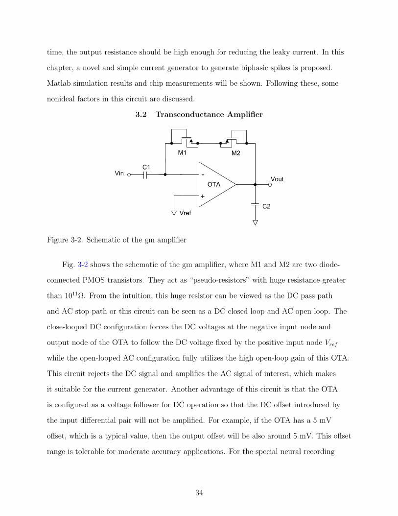
3.2 Transconductance Amplifier
Vin
Vref
OTA
+
-Vout
M2M1
C1
C2
Figure 3-2. Schematic of the gm amplifier
Fig. 3-2 shows the schematic of the gm amplifier, where M1 and M2 are two diode-
connected PMOS transistors. They act as “pseudo-resistors” with huge resistance greater
than 1011Ω. From the intuition, this huge resistor can be viewed as the DC pass path
and AC stop path or this circuit can be seen as a DC closed loop and AC open loop. The
close-looped DC configuration forces the DC voltages at the negative input node and
output node of the OTA to follow the DC voltage fixed by the positive input node Vref
while the open-looped AC configuration fully utilizes the high open-loop gain of this OTA.
This circuit rejects the DC signal and amplifies the AC signal of interest, which makes
it suitable for the current generator. Another advantage of this circuit is that the OTA
is configured as a voltage follower for DC operation so that the DC offset introduced by
the input differential pair will not be amplified. For example, if the OTA has a 5 mV
offset, which is a typical value, then the output offset will be also around 5 mV. This offset
range is tolerable for moderate accuracy applications. For the special neural recording
34

application in this biphasic spike generator, if the thresholds are set to hundreds of mV,
this 5mV-offset is also tolerable.
+
-
Vin C1 VoutR
CLr0
GmVxVx
Ix
Figure 3-3. Equivalent circuit of the gm amplifier
To understand to which extent this gm amplifier works, a detailed transfer function
analysis is conducted. To simplify the derivation, the OTA is modelled as one with
transconductance of gm and output resistance of r0. The equivalent circuit of the gm
amplifier is shown in Fig. 3-3 where the “pesudo-resistor” is represented by R and the load
capacitor (or integrating capacitor) by CL.
First note that
(Ix −GmVx)(r0
1 + jωCLr0
) + IxR = Vx. (3–1)
that is,
Rx =R + ( r0
1+jωCLr0)
1 + Gm( r0
1+jωCLr0). (3–2)
Here Rx is the impedance looking into the right side of the circuit. Based on this equation,
the total current Ix can be written as
Ix =Vin
1jωC1
+ Rx
. (3–3)
Deriving the relationship between Vin and Vout gives:
Vout = Vin − Ix(R +1
jωC1
). (3–4)
35

Combining Eq. 3–1 to Eq. 3–4, the total transfer function of this gm amplifier can be
written as
H(ω) =Vout
Vin
=jωr0C1(1−GmR)
(1 + jωC1R)(1 + jωCLr0) + r0(Gm + jωC1). (3–5)
Based on this transfer function, it is apparent that this system has one zero and two poles.
The zero lies at the origin so that the gain first increases at 20dB per decade. It is difficult
to locate these two poles for the general case. However, in some special cases, these two
poles can be solved.
To solve for these two poles, the denominator is set equal to zero:
(1 + jωC1R)(1 + jωCLr0) + r0(Gm + jωC1) = 0. (3–6)
If the parameters have these typical values:
R = 1013Ω; (3–7)
C1 = CL = 20pF ; (3–8)
Gm = 30×10−6Ω−1, (3–9)
r0 = 2.67×10⁹Ω, (3–10)
Eq. 3–6 can be simplified as
(jω)2RC1r0CL + (jω)RC1 + r0Gm ' 0. (3–11)
which can be further simplified as
(jω +r0Gm
RC1
)(jω +1
r0CL
) ' 0. (3–12)
Two poles are straightforward:
| ωp1 |= r0Gm
RC1
; | ωp2 |= 1
r0CL
. (3–13)
36
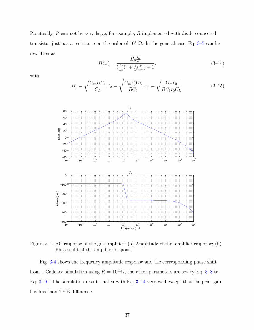
Practically, R can not be very large, for example, R implemented with diode-connected
transistor just has a resistance on the order of 1011Ω. In the general case, Eq. 3–5 can be
rewritten as
H(ω) =H0
jωω0
( jωω0
)2 + 1Q
( jωω0
) + 1. (3–14)
with
H0 =
√GmRC1
CL
; Q =
√Gmr2
0CL
RC1
; ω0 =
√Gmr0
RC1r0CL
. (3–15)
10−2
10−1
100
101
102
103
104
105
106
107
−60
−40
−20
0
20
40
60
80(a)
Gai
n (d
B)
10−2
10−1
100
101
102
103
104
105
106
107
−500
−400
−300
−200
−100
0(b)
Pha
se (
deg)
Frequency (Hz)
Figure 3-4. AC response of the gm amplifier: (a) Amplitude of the amplifier response; (b)Phase shift of the amplifier response.
Fig. 3-4 shows the frequency amplitude response and the corresponding phase shift
from a Cadence simulation using R = 1011Ω, the other parameters are set by Eq. 3–8 to
Eq. 3–10. The simulation results match with Eq. 3–14 very well except that the peak gain
has less than 10dB difference.
37

3.3 Integrate-and-Fire Neuron
3.3.1 Ideal Integrate-and-Fire Neuron and Nonidealities
x(t)
)(2
H)(1
H
1p
y(t)
2p
Figure 3-5. Ideal two-stage system for spike representation
The ideal integrate-and-fire (IF) neuron can be considered as a low-pass filter with a
pole at zero and the output resistance of infinity. Therefore all the input current goes into
the capacitor. In addition, to satisfying the bandwidth requirement, the signal must be
filtered first. The ideal two-stage IF system can be shown as Fig. 3-5.
Comparator
Vcap
Vth
+
-M1
Current x(t)
pulse
C
Figure 3-6. Schematic of the integrate-and-fire (IF) neuron
In the time domain, the operation of this IF neuron can be simply described as
follows. Once the voltage on the load capacitor Vcap crosses the threshold Vth, a spike is
generated and the voltage is reset to the analog ground. After some refractory period, the
38

neuron begins to integrate again (see Fig. 3-6). The spike times tie and tib must satisfy the
following relation:
∫ tie
tib
x(t)
Cdt = Vth. (3–16)
In fact, after the neuron is reset, the new integration process can be viewed as the
response with input of x(t) and the system impulse response h(t). In the ideal IF neuron,
the impulse response is 1sC
in the s-domain and 1Cu(t) in the time domain. The system
response with x(t) as input can be written as Eq. 3–16.
There are two signal reconstruction methods from the spike train: the iterative
method and the close-form or weighted low-pass kernel WLPK method. Interested readers
can find a detailed discussion in [5] and [15]. For the reader’s convenience, the WLPK
method is briefly listed here.
Assume the pulse width τ is much less than the pulse time interval and can be
ignored, the spike train output can be written as
p(t) =∑i∈Z
δ(t− ti). (3–17)
A sufficient boundary condition for perfect reconstruction requires:
ti+1 − ti ≤ 1
2fmax
, ∀i (3–18)
where fmax in the maximum frequency of the bandlimited input signal x(t). Let∫ ti+1
ti
x(t)C
dt
= Vth,h′(t) = 2fmaxsinc(2πfmaxt), and si = (ti+1 + ti)/2.
H = [h′(t− si)]T (3–19)
Aij =
∫ tj+1
tj
h′(t− si)dt (3–20)
x(t) = CVthA−1H (3–21)
39

Often A is not full rank and regularization-type techniques are necessary to compute the
inverse [15].
Following the above reconstruction procedure, the Matlab simulation can reconstruct
the original signal x(t) with SER (signal to error power ratio) of 103dB. However, in
a realistic system, there is always finite output resistance due to the current generator
block. During the integration process, the resistor leaks some current and introduces an
error in reconstruction. This neuron model is called the leaky IF neuron. For example,
if the OTA is used to generate the current, the output resistance of the integrator is the
output resistance of the OTA, which is normally very large (see Fig. 3-7). In this case,
the integration is no longer an ideal process. The voltage on the load capacitor is in fact
the convolution of the current and the system impulse response e− t
r0C . The signal can still
be perfectly reconstructed if the value of r0 is known exactly. The detailed analysis for
this problem can be found in [15]. Actually, this leaky IF model can be used to relax the
constraint on the amplifier. For example, a resistance-known resistor can be intentionally
added parallel to the load capacitor. In this case, the added resistance is much less than
the OTA’s output resistance, and the leakage from the OTA’s output resistance can be
ignored. Since the added resistance is already known, it can be directly used for perfect
reconstruction. The other benefit of using this model is that the leakage can reduce the
output spike rate, which can further relax the requirement on the power consumption and
the communication bandwidth.
3.3.2 Biphasic Integrate-and-Fire Neuron and Nonideality Analysis
Replacing the current source in Fig. 3-1 by Fig. 3-2 leads to the biphasic IF neuron
implementation. This current generator is a second-order system and the output resistance
is affected by the feedback, so that the analysis will be more complicated.
First, the integration process needs to be analyzed before further analysis. Every time
after the neuron is reset, the voltage on the capacitor follows the convolution between
the input signal Vin(t) and the system response h(t). So, the first step is to estimate the
40

ComparatorVcap
Vth
+
-M1
Current x(t)
pulse
Cr0
OTAVin(t)
Figure 3-7. Schematic of the practical IF neuron
system impulse response h(t). Based on Eq. 3–11, the s-domain transfer function is:
H(s) =Vout(s)
Vin(s)=
sr0C1(1−GmR)
(1 + sC1R)(1 + sCLr0) + r0(Gm + sC1). (3–22)
With the assumptions that GmR À 1, RC1 À CLr0, r0C1, r0Gm À 1 and Gm
RCLÀ 1
4C1r20,
which are true in our application, the transfer function can be further simplified as
H(s) =Vout(s)
Vin(s)
≈ − sr0C1GmR
s2C1RCLr0 + sC1R + r0Gm
= −Gm
CL
s
(s + 12CLr0
)2 + ( Gm
C1RCL− 1
4C21r2
0)
≈ −Gm
CL
s
(s + 12CLr0
)2 + Gm
C1RCL
= −Gm
CL
s + 12CLr0
(s + 12CLr0
)2 + Gm
C1RCL
−1
2CLr0
(s + 12CLr0
)2 + Gm
C1RCL
(3–23)
Consider that 12CLr0
√C1RCL
Gm¿ 1, the impulse response can be simply written as
h(t) = −Gm
CL
e− t2CLr0 cos(
√Gm
C1RCL
t)− 1
2CLr0
√C1RCL
Gm
e− t
2CLr0 sin(
√Gm
C1RCL
t)
≈ −Gm
CL
e− t2CLr0 cos(
√Gm
C1RCL
t) t À 0 (3–24)
41
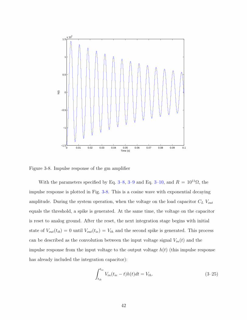
0 0.01 0.02 0.03 0.04 0.05 0.06 0.07 0.08 0.09 0.1−1.5
−1
−0.5
0
0.5
1
1.5x 10
6
Time (s)
h(t)
Figure 3-8. Impulse response of the gm amplifier
With the parameters specified by Eq. 3–8, 3–9 and Eq. 3–10, and R = 1011Ω, the
impulse response is plotted in Fig. 3-8. This is a cosine wave with exponential decaying
amplitude. During the system operation, when the voltage on the load capacitor CL Vout
equals the threshold, a spike is generated. At the same time, the voltage on the capacitor
is reset to analog ground. After the reset, the next integration stage begins with initial
state of Vout(tib) = 0 until Vout(tie) = Vth and the second spike is generated. This process
can be described as the convolution between the input voltage signal Vin(t) and the
impulse response from the input voltage to the output voltage h(t) (this impulse response
has already included the integration capacitor):
∫ tie
tib
Vin(tie − t)h(t)dt = Vth. (3–25)
42

If r0 and R are infinite, the impulse response is simply a step function, and the integration
is ideal. In the above equation, the integration does not represent the IF neuron’s integra-
tion process, but means the convolution between the input and the impulse response. Or
the above equation can be rewritten as a more familiar format:
∫ tie
tib
i(t)dt
CL
= Vth. (3–26)
where i(t) means the corresponding current integrated over the integration capacitor. The
integration in this equation is used to represent the IF neuron’s integration process. The
expression of i(t) can be derived from Eq. 3–24 to Eq. 3–26.
The close-form reconstruction algorithm for the biphasic spike train is very similar
to that of the unidirectional spike train. Chen has the detailed proof in [5]. The main
difference is that Vth has just one value in the unidirectional spike train (see Eq. 3–21)
while it have two values in the biphasic spike train. If the leaky current is not considered
in the reconstruction algorithm, the achieved SER is around 80dB. The error signal is
defined as the difference between the original signal and the reconstructed signal. The
SER is the power ratio between the original signal and the error signal.
Fig. 3-9 shows the reconstructed signal compared to the original signal. The original
signal is the superposition of five sine waves with frequency of 0.1 Hz, 10 Hz, 100Hz,
1000Hz and 5000Hz respectively and amplitude of 0.03V. The positive and negative
thresholds are 0.4V and -0.4V respectively. The step size in the Matlab simulation is
1ns. The total number of spikes within 1.8 ms is 171. The circuit parameters used for
the Matlab simulation are the same as those used for generating the impulse response
in Fig. 3-8. The original signal and the reconstructed signal are normalized for easy
comparison.
43

0 0.2 0.4 0.6 0.8 1 1.2 1.4 1.6 1.8−0.4
−0.2
0
0.2
0.4(a)
0 0.2 0.4 0.6 0.8 1 1.2 1.4 1.6 1.8−1
−0.5
0
0.5
1(b)
0 0.2 0.4 0.6 0.8 1 1.2 1.4 1.6 1.8−1
−0.5
0
0.5
1
1.5
2x 10
−4 (c)
Time (ms)
OriginalReconstructed
Am
plitu
de (
V)
Am
plitu
de (
V)
Am
plitu
de (
V)
Figure 3-9. Simulated time domain results: (a) The signal on the load capacitor Vcap; (b)Comparison between the original signal and the reconstructed signal (bothsignals are normalized); (c) Errors between the original signal and the recon-structed signal.
If the circuit parameters are known, the coefficient matrix A in Eq. 3–20 can be
recalculated using the following equation:
Aij =
∫ tj+1
tj
h′(t− si)h(t− tj+1)dt (3–27)
This coefficient matrix is calibrated with the impulse response, so that the reconstruction
signal can achieve much higher SER. The reconstructed signal using this matrix is shown
in Fig. 3-10 and the achieved SER is 102dB.
Even if it is possible that the original signal can be perfectly reconstructed from
the spike train given known parameters, in practice the parameters r0 and R are usually
signal- and process-dependent terms and exhibit some nonlinearity and unpredictability.
44
0 0.2 0.4 0.6 0.8 1 1.2 1.4 1.6 1.8−0.6
−0.4
−0.2
0
0.2
0.4
0.6
0.8
1(a)
0 0.2 0.4 0.6 0.8 1 1.2 1.4 1.6 1.8−1.5
−1
−0.5
0
0.5
1
1.5x 10
−5 (b)
Time (ms)
OriginalReconstructed
Am
plitu
de (
V)
Am
plitu
de (
V)
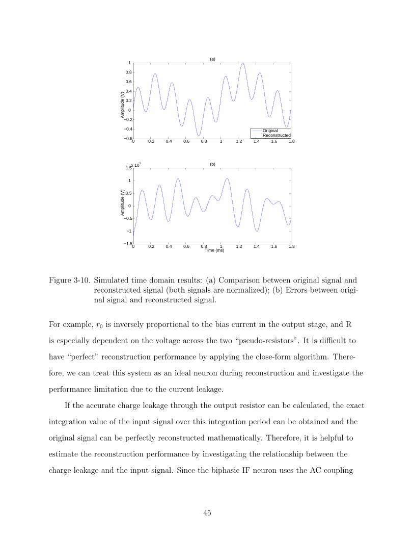
Figure 3-10. Simulated time domain results: (a) Comparison between original signal andreconstructed signal (both signals are normalized); (b) Errors between origi-nal signal and reconstructed signal.
For example, r0 is inversely proportional to the bias current in the output stage, and R
is especially dependent on the voltage across the two “pseudo-resistors”. It is difficult to
have “perfect” reconstruction performance by applying the close-form algorithm. There-
fore, we can treat this system as an ideal neuron during reconstruction and investigate the
performance limitation due to the current leakage.
If the accurate charge leakage through the output resistor can be calculated, the exact
integration value of the input signal over this integration period can be obtained and the
original signal can be perfectly reconstructed mathematically. Therefore, it is helpful to
estimate the reconstruction performance by investigating the relationship between the
charge leakage and the input signal. Since the biphasic IF neuron uses the AC coupling
45

structure, only the AC component of the signal can affect the reconstruction performance.
Assume that Vin and Vin are the value of Vin(t) and the value of the first-order derivative
at t = ti respectively. When the integration period is very short, Vin(t) can be assumed to
be a linear function of time t, and it can be approximated as Vin + Vin(t − ti) for the i-th
integration period. To simplify the derivation, some Taylor series approximations are used:
ex ≈ 1 + x, ifx ¿ 1 (3–28)
and
cos(x) ≈ 1− x2
2, ifx ¿ 1 (3–29)
To simplify the notation, a and b are used to represent − 12CLr0
and√
Gm
C1RCLre-
spectively in the following derivation. Based on the integration equation 3–25, we can
obtain:
θ = CLVth
= −Gm
∫ ti+1
ti
Vin(t)ea(ti+1−t)cos(b(ti+1 − t)dt
≈ −Gm
∫ ti+1
ti
(Vin + Vin(t− ti))ea(ti+1−t)cos(b(ti+1 − t))dt
= −Gm
∫ Ti
0
(Vin + Vint)ea(Ti−t)cos(b(Ti − t))dt
= −Gm
∫ Ti
0
Vinea(Ti−t)cos(b(Ti − t))dt−Gm
∫ Ti
0
Vintea(Ti−t)cos(b(Ti − t))dt
= −Gm(Vin + TiVin)
∫ Ti
0
eatcos(bt)dt + GmVin
∫ Ti
0
teatcos(bt)dt
≈ −Gm(Vin + TiVin)
∫ Ti
0
(1 + at)(1− b2t2
2)dt
+GmVin
∫ Ti
0
t(1 + at)(1− b2t2
2)dt
≈ −Gm(Vin + TiVin)(Ti +a
2Ti
2 − b2
6Ti
3) + GmVin(T 2
i
2+
aT 3i
3)
≈ −GmVin(Ti +a
2Ti
2 − b2
6Ti
3)−GmVin(1
2Ti
2 +a
6Ti
3) (3–30)
46

Where the higher order of Ti than 4-th are ignored in the last step. Since the integration
is treated as ideal process in reconstruction, the accurate integration of Vin(t) over the i-th
integration period is:
θi = Gm
∫ ti+1
ti
Vin(t)dt
≈ Gm
∫ ti+1
ti
(Vin + Vin(t− ti))dt
= Gm
∫ Ti
0
(Vin + Vint)dt
= GmVinTi + GmVinT 2
i
2(3–31)
Therefore the leakage charge for i-th integration period is:
| θi | − | θ | = GmVin(a
2T 2
i −b2
6T 3
i ) + GmVina
6T 3
i (3–32)
The reason that absolute value is used here is that the output current has reversed phase
compared to the input. The error is just introduced by absolute charge.
The corresponding noise power due to the leakage charge can be calculated as (using
Eq. 3–21):
Pnoise,leakage = E[(Vin(t)− Vin(t))2]
=1
G2m
E[(i(t)− i(t))]
=1
G2m
E[(∑
i
h′i(t)(θi − θ))2]
=1
G2m
E[(∑
i
(h′i(t))2)]E[(θi − θ)2]
≈∑
i
E[(h′i(t))2]E[(Vin
a
2T 2
i )2] + E[(Vinb2
6T 3
i )2] + E[(Vina
6T 3
i )2]
≈∑
i
E[(h′i(t))2]E[(Vin
a
2(CLVth
GmVin
)2)2] + E[(Vinb2
6(CLVth
GmVin
)3)2]
+E[(Vina
6(CLVth
GmVin
)3)2] (3–33)
47

where the approximation is made due to CLVth ≈ GmVinTi. The signal power is:
Psignal = E[(Vin(t))2]
=1
G2m
E[(∑
i
h′i(t)θi)2]
≈ 1
G2m
E[(∑
i
h′i(t))2](CLVth)
2 (3–34)
The SER (signal to error ratio) due to the leakage is:
SERleakage =Psignal
Pnoise,leakage
≈ 1
E[a2
4( CLVth
GmVin)2] + E[ b4
36( CLVth
GmVin)4] + E[( Vin
Vin)2 a2
36( CLVth
GmVin)4]
=1
V 2th
16G2mr2
0E[ 1
V 2in
] +C2
LV 4th
36G2mR2C2
1E[ 1
V 4in
] +C2
LV 4th
144G4mr2
0E[
V 2in
V 6in
]
≈ 1V 2
th
16G2mr2
0E[ 1
V 2in
] +C2
LV 4th
36G2mR2C2
1E[ 1
V 4in
](3–35)
where E[(∑
i h′i(t))
2] ≈ ∑i E[(h′i(t))
2] is used for the first approximation. During the
second approximation, the last term of the denominator is ignored because it is very small
compared to the first two terms.
Eq. 3–35 shows the dependence of the SER on the parameters of the biphasic IF
neuron and input signal. The SER can be improved by increasing the OTA output
resistance r0 or increasing the bypass resistance R. This argument is consistent with
Eq. 3–24. Based on Eq. 3–24, when r0 increases, the slower exponential decay will
introduce less leakage charge. If R is increased, the cosine wave has smaller frequency
and the slower cosine decay can improve the SER. Larger C1 also leads to a larger SER
by reducing the cosine wave frequency. Increasing Gm or reducing CL also reduces the
charge leakage and increases the SER. Actually both of Gm and CL have two different
effects. First, they determine the gain and therefore affect the spike frequency. On the
other hand, they also alternate the cosine wave frequency of the impulse response and
change the leakage error. However, compared to the second effect, the first one is more
48

dominant. Smaller Vth can increase the spike frequency and increase the SER. Eq. 3–35
also indicates that the SER is proportional to E[V 2in]. The reason is that a larger input
signal amplitude increases the spike frequency and hence increases the SER. It is shown
that the unidirectional-spike reconstructed signal SER decreases when the input signal
frequency increases [15]. However, in the biphasic IF representation, the frequency has
little effect on the SER, which can be seen from Eq. 3–35. To verify the SER’s frequency
independence, the results from a Matlab simulation and Eq. 3–35 are given in Fig. 3-11.
The parameters of the biphasic IF neuron are: C1 = 20pF, Vth = ±0.4V, Gm = 30uΩ−1, r0
= 2.6× 10⁹Ω, R = 1011Ω, and the input is a single tone with different frequency and same
amplitude of 30mV.
102
103
104
20
30
40
50
60
70
80
90
Sine wave frequency (Hz)
SE
R (
dB)
Simulation
Equation
Figure 3-11. signal-to-noise ratio (SER) vs. sine wave frequency
Based on the above analysis, the direction to improve SER is clear. Due to the
practical signal properties and available CMOS process technology, there are not many
49

options to combine. For example, the average firing rate is related to the communication
bandwidth of the readout circuit and is usually a predefined number. Therefore, reducing
Vth, increasing Gm and reducing CL increases SER by increasing the spike rate are not
good choices under the bandwidth constraint. r0 and R can be changed without affecting
the spike rate, however, the available fabrication technology and circuit design prohibit us
from freely choosing the values. This leaves C1 as the only choice. However, limited chip
layout area restricts large capacitance.
Several simulations are run in Matlab to validate the above discussion. Without
additional declarations, the parameters of the biphasic IF neuron are: C1 = 20pF, Vth =
±0.4V, Gm = 30uΩ−1, r0 = 2.6 × 10⁹Ω, R = 1011Ω, and the signal is the superposition
of five sines wave with the same amplitude of 30mV and different frequencies of 0.1Hz,
10Hz, 100Hz, 1000Hz and 5000Hz. In the following figures the dotted line with stars and
the solid line with circles represent the results from the Matlab simulation and Eq. 3–35,
respectively. All the Matlab simulations were run with the step size of 1ns.
Fig. 3-12 shows the dependence of the SER on the bypass resistor R. The equation
matches the simulation very well with a slope of 20dB/decade. Both curves predict that
there is a SER saturation when R is above 1012Ω. This is due to other nonideal factors.
Fig. 3-13 shows the dependence of the SER on the OTA output resistor r0. When
r0 < 109Ω, the equation matches the simulation very well with a slope of 20dB/decade.
Both curves predict that there is a SER saturation when R is above 1010Ω. However, there
is around 12dB difference between the saturation SER values. Compared to Fig. 3-12,
the saturation here occurs earlier than that of the bypass resistor. Other than that, SER
corresponding to the saturation output resistor is 3dB lower than that of bypass resistor
from the Matlab simulation. These differences mean that the bypass resistor plays a more
important role in increasing SER.
50

108
109
1010
1011
1012
1013
35
40
45
50
55
60
65
70
75
80
85
90
Bypass resistance (Ohm)
SE
R (
dB)
Equation
Simulation
Figure 3-12. SER vs. bypass resistance
Fig. 3-14 shows the dependence of SER on the input capacitor C1. When C1 > 0.1nF,
the equation matches the simulation well. Otherwise, the difference between the equation
and the simulation is 8dB maximum. There is also a SER saturation in this figure.
3.4 Operational Transconductance Amplifier Design
Based on the previous discussion about SER, it is apparent that one option in OTA
design is to make the output resistance as high as possible. Alternatively, we can add an
explicit leak resistance of known value. Then the requirement of high output resistance
of the OTA can be relaxed. As we discussed in the previous section, this leaky integrator
will bring other benefits. The other factors under consideration are power consumption,
transconductance Gm, noise issues and stability.
51

107
108
109
1010
1011
1012
45
50
55
60
65
70
75
80
85
90
95
100
Output resistance (Ohm)
SE
R (
dB)
Equation
Simulation
Figure 3-13. SER vs. output resistance
3.4.1 Circuit Description
Fig. 3-15 shows the schematic of the OTA used in the biphasic IF neuron. The OTA
is a typical single-stage CMOS amplifier with a P-type input differential pair operating
from a ±2.5V power supply. The input differential pair is loaded with a cascode current
mirror. Another cascode current mirror is used to convert the differential output to
single-ended output. The cascode current mirrors give a high output resistance for this
OTA:
r0 = Rout10 ‖ Rout14 (3–36)
where both Rout10 and Rout14 are the output resistance from a cascode current mirror,
thus:
Rout10 ≈ gm10ro12ro10 (3–37)
52

10−12
10−11
10−10
10−9
70
72
74
76
78
80
82
84
86
Input capacitance (F)
SE
R (
dB)
EquationSimulation
Figure 3-14. SER vs. input capacitance
Rout14 ≈ gm14ro6ro14 (3–38)
This OTA just has one dominant pole at ω = 1r0CL
, which guarantees that it is stable in
most cases.
3.4.2 Noise and Power Consideration
M7∼M10 and M13, M14 in Fig. 3-15 are common gate transistors, and their thermal
noise contribution is negligible. The input pair M1 and M2 have identical size and their
transconductance is denoted as gm1. The cascode current mirrors M3∼M8 also have
identical size and the transconductance is denoted as gm3. The transconductance of M11
and M12 is denoted as gm11 since they are also matched in the circuit design. Therefore,
the OTA input-referred thermal noise should be:
v2ni,OTA = [
16κT
3gm1
(1 + 2gm3
gm1
+gm11
gm1
)]∆f (3–39)
53

Vout
CL
VDD
Vin- Vin+M1 M2
M3 M4M5 M6
M13 M14
M9 M10
M11 M12
M7M8
Ibias
VSS
Figure 3-15. Schematic of the OTA
If gm1 is increased or gm11 and gm3 are decreased, the input-referred thermal noise can
be decreased. The most straightforward approach is to increase (W/L)1,2 or to decrease
(W/L)3∼8,11,12. However, noticing that M11 is associated with the first nondominant
pole and M3, M4 are associated with the second nondominant poles, reducing the sizes
of these transistors will reduce the transconductance of these transistors and push these
nondominant poles to zero, possibly degrading the stability. Consequently, there is a
tradeoff between the input-referred thermal noise and stability.
The flicker noise is another major noise source in low-frequency CMOS circuits. It
can be decreased by increasing the areas of the CMOS transistors. However, the areas are
also related to the nondominant poles as discussed above, which puts a restriction on the
flicker noise performance.
Power consumption is another big concern in low-power circuit design. The static
power consumption of this OTA is directly determined by the bias current, which is set to
8 µA in the simulation and chip measurement. Reducing this current can reduce the power
54

consumption. On the other hand, reducing the bias current can also increase the output
resistance of the OTA because r0 ∝ 1/I. Fig. 3-13 shows that higher SER can be achieved
when the OTA’s output resistance increases.
However, there are also some drawbacks on reducing the bias current or power
consumption. The most important drawback is related to the transconductance of
the OTA. Eq. 3–35 indicates that the reconstruction SER is directly proportional to
G2m. Therefore, higher a Gm can generate higher SER from the reconstructed signal.
Increasing the bias current can directly increase the transconductance. Actually, when
Gm increases, more output spikes can be generated, which again increases the dynamic
power consumption. The above discussion indicates that we have to trade off the power
consumption with the SER.
3.5 Chip Layout
The layout of this chip with pads is shown in Fig. 3-16. There are three components:
the gm amplifier, the comparators and the digital control block. They are powered by
individual power supply to reduce the cross coupling, and each power supply has its own
bypass capacitor. Guard rings are also used to eliminate the kick back noise from the
digital circuit. These three parts are separated as far as possible. The total layout area
including the pads is 2.25mm2.
3.6 Cadence Simulation Results
The digital control circuits of the single-channel biphasic IF neuron were designed
by Chen [22]. This digital block is concatenated to the gm amplifier, thus finishing the
single-channel circuit design with the 0.6 µm CMOS process. The Cadence simulation
is run for the single channel. The input signal is a sine wave with amplitude of 20mV.
The frequency is swept from 1KHz to 10KHz and the input signal lasts for 2ms. The bias
current of the gm block is set to 8uA and the integration capacitor is set to 20pF. The
spike train is then directly read out and the signal is reconstructed in Matlab using the
closed-form algorithm. The 4-parameter sine wave fitting method is used to estimate the
55

Figure 3-16. Layout of the single-channel biphasic IF neuron chip
input signal from the reconstructed single tone signal by finding the best-fitting sine wave
[23]:
x(t) = A cos(ωt + θ) + C (3–40)
The difference between the reconstructed signal and the fitted signal are defined as the
error. The SER (signal to error ratio) is defined as the power ratio of the fitted signal to
the error. The SER vs. input signal frequency is shown in Fig. 3-17. The reconstructed
SER values range from 51dB to 57.5dB, which means more than 8 ENOB (effective
number of bits). The difference between the SER in Fig. 3-17 and the Matlab simulated
SER is due to the nonlinearity of the gm block and the signal dependence of the analog
comparator. The finite number of pulses and the computational precision of MATLAB
56
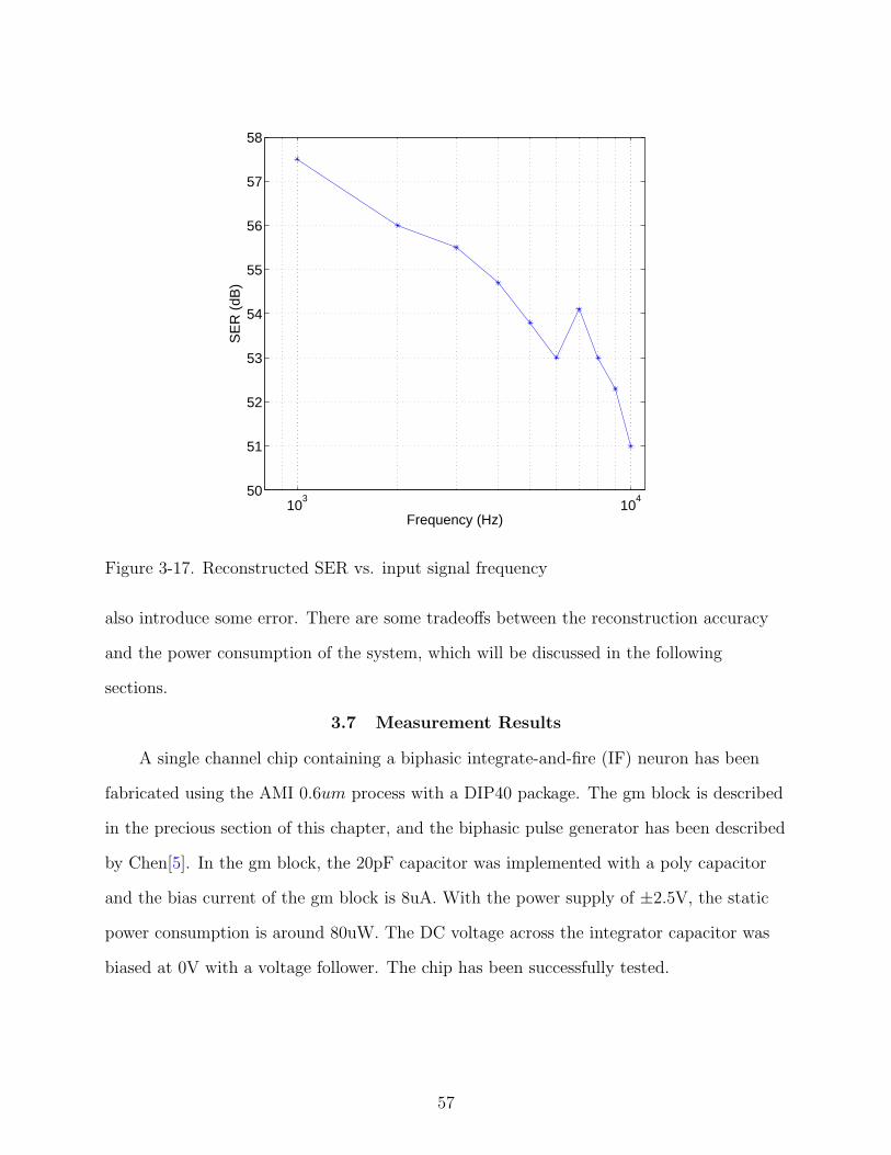
103
104
50
51
52
53
54
55
56
57
58
Frequency (Hz)
SE
R (
dB)
Figure 3-17. Reconstructed SER vs. input signal frequency
also introduce some error. There are some tradeoffs between the reconstruction accuracy
and the power consumption of the system, which will be discussed in the following
sections.
3.7 Measurement Results
A single channel chip containing a biphasic integrate-and-fire (IF) neuron has been
fabricated using the AMI 0.6um process with a DIP40 package. The gm block is described
in the precious section of this chapter, and the biphasic pulse generator has been described
by Chen[5]. In the gm block, the 20pF capacitor was implemented with a poly capacitor
and the bias current of the gm block is 8uA. With the power supply of ±2.5V, the static
power consumption is around 80uW. The DC voltage across the integrator capacitor was
biased at 0V with a voltage follower. The chip has been successfully tested.
57

102
103
104
30
35
40
45
50
55
Frequency (Hz)
SE
R (
dB)
20mVp−p input40mVp−p input
Figure 3-18. SER vs. single tone frequency
3.7.1 Single-Tone Input
The first measurements were for a single tone input. An Agilent 33220A signal
generator was used in the testing. The single tone frequency was swept from 50Hz
to 7000Hz and the input amplitude are 20mV peak to peak and 40mV peak to peak
respectively. The threshold of the biphasic IF neuron was ±0.4V. The output from the
signal generator was directly coupled into the chip input. The voltage signal was first
converted into current signal and the generated current signal was then integrated on the
capacitor. The biphasic IF neuron generates the biphasic spike output. The spike output
is captured by an Agilent 1693A logic analyzer working in the asynchronous mode with
sampling rate of 5ns. The collected spikes were then fed into Matlab and the signal was
reconstructed with the close-form algorithm. For each frequency, around six periods of
signal were reconstructed. The reconstructed SER is shown in Fig. 3-18. From this figure,
it is apparent that the tested SER is very close to the simulation results, which proves
that the previous analysis is correct. In the high frequency region, the 40mV peak to peak
58

102
103
104
30
40
50
60
70
80
90
Frequency (Hz)
Spi
ke r
ate
(Kpu
lse/
s)
20mVp−p input
40mVp−p input
Figure 3-19. Spike rate vs. sine wave frequency
input can generate as high as 55dB reconstructed signal (which means around 9 ENOB),
and the 20mV peak to peak input can also has 50dB SER, which is very close to the
simulated 51dB. During the low frequency region, the SER is a little bit lower. There is
no direct relationship between the SER and the input signal amplitude. The statistics of
the spike rate are also shown in Fig. 3-19. It is very clear that the spike rate reduces with
increasing frequency. This reduction trend is not apparent in the low frequency region
but it is more obvious in the high frequency region. When the input signal amplitude is
doubled, the spike rate is almost doubled as expected.
Fig. 3-20 shows an example of the biphasic pulse train output and the offline recon-
structed signal. The input signal is a 1KHz sine wave with 20mV peak-to-peak amplitude.
The red curve Fig. 3-20 (b) is the reconstructed sine wave from the pulse train showed in
Fig. 3-20 (a) and the blue curve is the 4-parameter fitting sine wave. Fig. 3-20 (c) is the
error between the reconstructed signal and the fitting signal. This reconstructed signal has
45dB SER.
59

0 0.5 1 1.5 2 2.5 3 3.5 4 4.5 5−1
0
1
Am
plitu
de
(a)
0 0.5 1 1.5 2 2.5 3 3.5 4 4.5 5−20
0
20
40
60
Am
plitu
de (
mV
)
(b)
0 0.5 1 1.5 2 2.5 3 3.5 4 4.5 5−0.1
0
0.1
Time (ms)
Am
plitu
de (
mV
)
(c)
Reconstructed
Fitted
Figure 3-20. Measured reconstruction time domain result example: (a) Pulse output; (b)Reconstructed single tone signal (red) and the 4-parameter fitted single tonesignal (blue); (c) Error.
One apparent result is that when the biphasic comparator threshold is reduced, the
output spike rate will be increased. The increasing spike rate requires more communi-
cation bandwidth. On the other hand, more output spikes also consume more dynamic
power. Therefore, it is beneficial to increase the comparator threshold to reduce the spike
rate.
In unidirectional IF neuron system, the AC signal is shifted by a DC component and
the integrated absolute current is a constant. The resulting spike rate is independent of
the input signal frequency. However, in the biphasic IF neuron system, when the input
signal changes from positive value to the negative value (or vice verse), the integrated
charge after the last spike gets canceled by the opposite-polar charge, therefore, the total
spike rate is dependent on the input signal frequency. when the input signal frequency
increases, the charge gets canceled more often, and the resulting spike rate reduces with
the increasing frequency. This analysis actually verifies the statistics from Fig. 3-19.
60

0.2 0.3 0.4 0.5 0.6 0.7 0.8 0.9 120
40
60
80
100
120
140
160
180
200
Threshold (V)
Spi
ke r
ate
(Kpu
lse/
s)
MeasurementEquation
Figure 3-21. Threshold vs. spike rate
When the input signal frequency is low and there are many output spikes generated
during each half period, the canceled charge can be neglected, the spike rate can be viewed
as frequency independent and it can be written as
Spikerate =2VinGm
π|Vth|CL
(3–41)
where Vin means the input signal amplitude. To verify the relationship between spike rate
and the comparator threshold, another test was conducted. In this testing, a 800Hz 40mV
peak-to-peak single tone was fixed as the input while the biphasic comparator threshold
was varied from ±0.2V to ±1.0V. The generated spike train was then collected with
the logic analyzer and the input signal was reconstructed with Matlab offline code. The
measurement result and the result from Eq. 3–41 with Gm = 60µS are shown in Fig. 3-21.
From this figure, the output spike rate decreases from 160Kpulses/s (with the threshold
of ±0.2V) to less than 40Kpulses/s (with the threshold of ±1.0V). This trend is similar to
the equation.
61

0.2 0.3 0.4 0.5 0.6 0.7 0.8 0.9 146
47
48
49
50
51
52
53
Threshold (V)
SE
R (
dB)
Figure 3-22. Threshold vs. SER
We are also interested in how the SER will change with the reduced spike rate.
The measurement result is shown in Fig. 3-22. The SER is reduced from 52dB to 47dB
with the increasing threshold and reducing spike rate, which is somewhat expected.
Fortunately, the SER does not vary very much. This testing provides us the relationship
between the spike rate (or communication channel bandwidth and power consumption)
and the reconstruction SER. It is apparent that the spike rate can be greatly reduced
without sacrificing the accuracy very much. Of course a limit will be reached where the
distance between spikes violates the sampling assumption.
3.7.2 Neural-Simulator Input
The specific application of this biphasic IF encoding is for neural signals. Neural
signals are composed of action potentials (the signal) and noise. Typically, the action
potential is about 50-500 µV in amplitude [3] and lasts for 1-1.5 ms [4]. With the biphasic
IF encoding, the output spike rate is supposed to be high in the action potential region.
On the other hand, if there is just noise during that period, the output spike rate is
62

ideally low to save the communication channel bandwidth. Since the action potential is
of interest, it is desired to reserve high communication bandwidth for them. It is assumed
that this biphasic IF encoding method can make full use of the communication channel
bandwidth.
Some measurements were conducted to evaluate the performance of this application.
The Bionic 128 Channel Neural Signal Simulator and an Agilent 1693A logic analyzer were
the two primary instruments in this testing setup. As discussed in the previous chapter,
the Neural Signal Simulator can provide a prerecorded neural signal. The action potential
output from this Neural Signal Simulator is around 200 µV peak-to-peak. This signal is
too tiny to generate a spike output. Based on the single tone testing, we think that the
reasonable input signal range is around 20mV peak-to-peak. The preamplifier design
by Chen [11] was used as the first stage to boost the neural signal and to convert the
differential neural signal to a single-ended signal. Following the output of the preamplifier
were the gm block and the biphasic IF block. An Agilent 1693A logic analyzer was used
to record the biphasic spike train. The collected spike train is then fed into Matlab offline
code. During the noise region, there were very few spike outputs and the time delay
between consecutive spikes can be greater than the Nyquist period of the input signal. As
a result, the convergent condition for close-form algorithm can not be met and we have to
use the iteration algorithm for reconstruction [5]. After careful comparison, it was found
that the reconstruction signal after the 5th iteration provides the best fidelity.
Fig. 3-23 shows an example of the biphasic pulse train output and the offline recon-
structed neural signal. In this example, the biphasic comparator threshold was set to
±0.4V. The shown signal lasts for 30ms. It is apparent that the measurement results ver-
ify the expectation. During the action potential region, there are high spike rate output;
on the other hand, when there is no interesting neural signal, the generated spike rate is
very sparse as expected. Since the noise region is not interesting to us, low signal fidelity
can be tolerated but the action potential regions are kept with higher accuracy. Statistical
63

0 0.005 0.01 0.015 0.02 0.025 0.03−1
−0.5
0
0.5
1
Am
plitu
de
(a)
0 0.005 0.01 0.015 0.02 0.025 0.03−1
−0.5
0
0.5
1x 10
−5
Time (s)
Am
plitu
de (
V)
(b)
Figure 3-23. Measured reconstruction time domain result example: (a) Pulse output; (b)Reconstructed neural signal.
measures have been used to compare the spike rate during different signal regions and
the measurement results are listed in Table 3-1. In this table, the biphasic comparator
threshold has been swept from ±0.2V to ±0.9V, and the spike rate has been calculated
during three different signal regions. One is so-called spike burst region, which means
that is a large number of action potentials generated in a sequence and each spike lasts
for 5ms. The second region is a noise region, where no action potentials are generated.
The last action potential region means the time region concentrating on each spike peak
which is normally 1ms. By comparing the spike rate difference among the three signal
regions, it is apparent that the communication bandwidth is saved. For example, when the
threshold is set to ±0.4V, the spike rate during the action potential is around 28Kpulses/s,
which is very high. However, if we average the spike rate during the total 5ms, the spike
rate is dropped to 6.9Kpulses/s. Within the same setup, the output spike rate is just
1.9Kpulses/s when there is no action potential.
64

Table 3-1. Spike-rate comparison
Threshold Spike burst Noise region Action potential
200mV 15.3K/s 6.5K/s 56.3K/s300mV 10K/s 2.3K/s 37.8K/s400mV 6.9K/s 1.9K/s 28K/s500mV 6.3K/s 1.8K/s 22.5K/s600mV 6.27K/s 1.4K/s 17.8K/s700mV 4.5K/s 1.3K/s 12K/s800mV 4.5K/s 0.6K/s 11.8K/s900mV 4.2K/s 0.5K/s 10K/s
Similar to the previous subsection, we still need to evaluate the performance of
this system. The difficulty in this case is that we do not have the original or fitting
signal, therefore the SER can not be used in this occasion. Even if the original signal
can be obtained, it is unfair to calculate the SER for all the signal region, because the
useful signal is just the action potential. This biphasic pulse encoding is intended to
achieve lower signal accuracy in noise region and to achieve higher signal fidelity in action
potential region.
Several methods have been proposed to compare the performance. The first method
is to calculate the cross-correlation coefficient between the reconstructed signal and the
neural signal. In this testing setup, the output from the neural simulator is predefined and
can be obtained by other uniformed sampling instrument. The Tucker-Davis Technologies
(TDT) RA8GA is used to record the neural simulator output with the sampling rate
of 24414.1Hz. Fig. 3-24 (a) shows one section of the TDT recorded neural signal. The
other signals shown in this figure are the reconstructed neural signal with threshold of
±0.3v, ±0.5V and ±0.9V respectively. The cross-correlation coefficient between the TDT
recorded neural signal and the reconstructed signal is listed in Table 3-2.
If the cross-correlation between two signals is one, they can be exactly the same or
they can differ in amplitude. To exclude the amplitude confusion, the second method is
used to calculate the mean absolute error (MAE) between the reconstructed signal and the
65
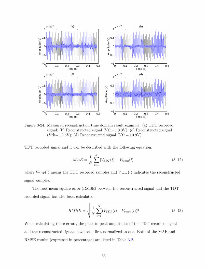
0 0.1 0.2 0.3 0.4 0.5−1
−0.5
0
0.5
1x 10
−5
Time (s)
(a)
Am
plitu
de (
V)
0 0.1 0.2 0.3 0.4 0.5−1
−0.5
0
0.5
1x 10
−5
Time (s)
(b)
Am
plitu
de (
V)
0 0.1 0.2 0.3 0.4 0.5−1
−0.5
0
0.5
1x 10
−5
Time (s)
(c)
Am
plitu
de (
V)
0 0.1 0.2 0.3 0.4 0.5−1
−0.5
0
0.5
1x 10
−5
Time (s)
Am
plitu
de (
V)
(d)
Figure 3-24. Measured reconstruction time domain result example: (a) TDT recordedsignal; (b) Reconstructed signal (Vth=±0.3V); (c) Reconstructed signal(Vth=±0.5V); (d) Reconstructed signal (Vth=±0.9V).
TDT recorded signal and it can be described with the following equation:
MAE =1
N
N∑i=1
|VTDT (i)− Vrecon(i)| (3–42)
where VTDT (i) means the TDT recorded samples and Vrecon(i) indicates the reconstructed
signal samples.
The root mean square error (RMSE) between the reconstructed signal and the TDT
recorded signal has also been calculated:
RMSE =
√√√√ 1
N
N∑i=1
(VTDT (i)− Vrecon(i))2 (3–43)
When calculating these errors, the peak to peak amplitudes of the TDT recorded signal
and the reconstructed signals have been first normalized to one. Both of the MAE and
RMSE results (expressed in percentage) are listed in Table 3-2.
66

Table 3-2. Statistics results on the reconstructed signals
Threshold cross-correlation coefficient MAE(%) RMSE(%)
200mV 0.84 3.3 4.7300mV 0.82 3.3 5.0400mV 0.83 3.4 4.9500mV 0.82 3.6 5.0600mV 0.80 3.8 5.4700mV 0.77 3.6 5.2800mV 0.75 4.5 6.0900mV 0.75 4.6 6.0
Actually, the noise regions in the TDT recorded signal and the reconstructed signals
are not important because they do not carry any useful information. Since there are
very few spike outputs generated in those regions, the reconstructed signals in those
regions should be poor in terms of signal fidelity. To better evaluate the signal fidelity
in the useful signal regions (action potentials), we can intentionally zero all the noise
regions and repeat the cross-correlation coefficients, MAE and RMSE calculation (in these
calculations, the signal length has been reduced correspondingly). The results from the
zeroed signals are listed in Table 3-3. Comparing the results in the above two tables, it is
apparent that the RMSE and MAE from the zeroed signals are always smaller than those
corresponding unmodified signals. On the other hand, the cross-correlation coefficients
from the zeroed signals are greater than those from unmodified signals. This observation
shows that the signal fidelity in the action potential regions is better than those in the
noise region as expected.
Another method to evaluate the reconstructed neural signal is to do some spike
sorting on the TDT recorded signal and the reconstructed signal. To some researchers,
it is the spike timing and the spike shape that are most important since the spike shape
indicates from which neuron this action potential is transmitted. In fact, spike sorting
has been used to achieve data reduction. In our evaluation process, if the spike sorting
results are very close (which means that if the action potential in the TDT recorded
signal is classified to be in the same class in the reconstructed signal case), it can be safely
67

Table 3-3. Statistics results on the zeroed reconstructed signals
Threshold cross-correlation coefficient MAE(%) RMSE(%)
200mV 0.88 1.7 4.0300mV 0.86 1.8 4.3400mV 0.87 1.7 4.1500mV 0.87 1.7 4.1600mV 0.85 1.9 4.5700mV 0.84 1.9 4.4800mV 0.80 2.1 4.8900mV 0.82 2.0 4.6
said that the key features of the action potential are kept. The output from the neural
simulator is predefined, and there are 3 classes of action potential in each channel. The
testing setup uses two channels for differential input and therefore there are total 6 classes
of action potentials in the TDT recorded signal and the reconstructed signal. Each class
of action potential is repeated after 30ms in the spike burst region. The achieved signal is
the 6 classes of spikes repeating themselves after 30ms, as can be seen in Fig. 3-24.
Figure 3-25. Spike sorting result based on reconstructed neural signal (Each panel of thefirst 6 panel indicates all the action potentials in that panel belong to thesame class; the last panel is the reconstructed signal.)
68

Table 3-4. Reconstructed neural signal spike sorting statistics (missing action potentials/total action potentials)
signal class 1 class 2 class 3 class 4 class 5 class 6
TDT recorded 0/17 0/16 0/16 0/16 0/16 0/16200mV 0/17 0/16 0/16 0/16 0/16 0/16300mV 0/17 0/16 0/16 0/16 0/16 0/16400mV 0/17 0/16 0/16 0/16 0/16 0/16500mV 0/17 0/16 0/16 0/16 0/16 0/16600mV 0/17 0/16 0/16 0/16 1/16 0/16700mV 0/17 0/16 0/16 0/16 2/16 0/16800mV 0/17 0/16 0/16 0/16 7/16 1/16900mV 0/17 2/16 0/16 0/16 11/16 4/16
A popular algorithm called Spike2 is used to do the spike sorting. Spike2 is a powerful
data acquisition system which can also do data capture, experiment control, recording and
analysis. Spike2 is also a popular neural software for spike detection and spike sorting.
Spike2 identifies and sorts single and multi-unit activity both on-line and off-line. It can
mark spikes using simple threshold crossings. For multi-unit activity, Spike2 contains tools
for sorting spikes based on the spike waveform shape. All events crossing a threshold are
captured and a combination of template matching and cluster cutting based on Principal
Component Analysis (PCA) is then used to sort spikes into different classes.
Fig. 3-25 shows an example of spike sorting results from Spike2. The neural signal is
reconstructed from the biphasic pulse output with threshold of ±0.4V. Each row of the
first six rows indicates all the action potentials belonging to the same template. It is clear
that there are total of six classes of action potentials found in the reconstructed neural
signal. In fact, all the action potentials are correctly sorted in this example. With the
extracted six templates, all the other reconstructed neural signals and the TDT recorded
signals are sorted by Spike2. The results are listed in Table 3-4. We can see that for
a threshold less than ±0.7V, the Spike2 sorting results of the reconstructed signal are
very close to that of TDT recorded signal. This comparison verifies that this biphasic IF
encoding works well for neural signal.
69

5 10 15 20 25 30 35 40−4
−3
−2
−1
0
1
2
3
4
5
6x 10
−6
Sample Number
Am
plitu
de
Figure 3-26. Comparison between the correctly identified action potential (blue solid line)and the missing action potentials (red dotted lines)
One may wonder what is the reason for the misclassified action potentials. We made
some comparisons here. Since most of the missing action potentials are from class 5, some
missing action potentials from this class are plotted to compare to the correctly classified
action potential. This plot is shown in Fig. 3-26. It is apparent that the amplitude is
responsible for the miss because the correctly identified action potential has a large
amplitude in both directions while the missing actions potentials have much less amplitude
in the negative direction.
Fig. 3-27 shows the six time-domain templates used in the Spike2 sorting. On each
template plot, the number on the top left marks the class number and these template
numbers are ordered to match with those in Fig. 3-25. The corresponding principal
component analysis on the six spike templates is shown in Fig. 3-28.
3.8 Practical issues
The previous Matlab simulation and circuit analysis are based on ideal assumptions.
After circuit measurements, we realized there is a gap between the measurement results
70

Figure 3-27. Six action potential classes (The number on the left top marks the classnumber)
and the simulation results. For example, the Cadence simulation shows that the recon-
structed SER is always greater than 50dB, while the chip measurement with the same
input signal and same setup shows an SER at most 50dB. Some practical issues contribute
to this difference. We will discuss these issues in this section.
3.8.1 Signal Dependent Reference of the Comparator
The biphasic IF encoding operation is realized using two identical comparators. If
Vth for example is set as one of the thresholds, when the voltage across the integration
capacitor crosses the threshold, the output of the comparator starts to change. When
the comparator output voltage reaches a high voltage, the logic analyzer reads out the
state and we assume that the recorded timing is the time when the integration voltage
reaches the threshold. However, this recording timing is somewhat later than the exact
71
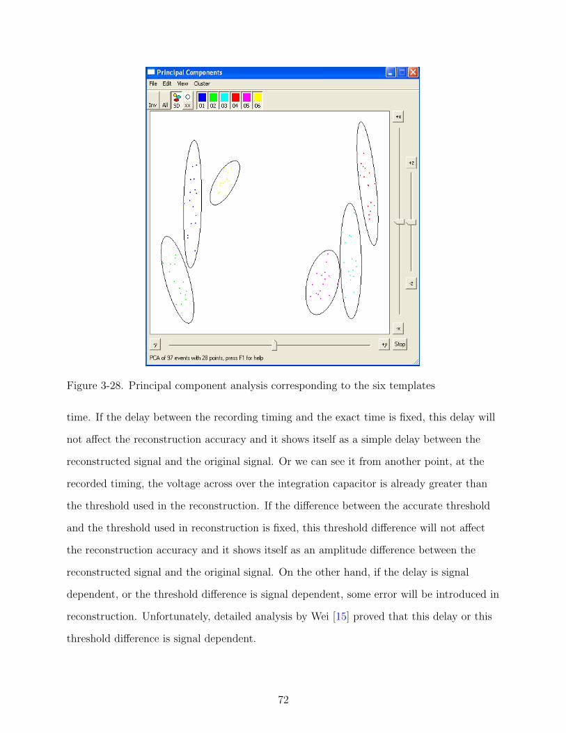
Figure 3-28. Principal component analysis corresponding to the six templates
time. If the delay between the recording timing and the exact time is fixed, this delay will
not affect the reconstruction accuracy and it shows itself as a simple delay between the
reconstructed signal and the original signal. Or we can see it from another point, at the
recorded timing, the voltage across over the integration capacitor is already greater than
the threshold used in the reconstruction. If the difference between the accurate threshold
and the threshold used in reconstruction is fixed, this threshold difference will not affect
the reconstruction accuracy and it shows itself as an amplitude difference between the
reconstructed signal and the original signal. On the other hand, if the delay is signal
dependent, or the threshold difference is signal dependent, some error will be introduced in
reconstruction. Unfortunately, detailed analysis by Wei [15] proved that this delay or this
threshold difference is signal dependent.
72

Realizing this error source, it is of interest to reduce this signal dependent error.
One apparent solution is to make the comparator’s transition fast. Following Wei’s [15]
analysis, the relationship between the bias current of the comparator and reconstructed
SER can be derived as
SER =πVth
√Ibiasβ
kVthCo,compfavg
. (3–44)
where
k = 1 +4(V 3
max − 1)
3(Vmax − 1)(Vmax + 1)2− 4
√2(V 2.5
max − 1)
2.5(Vmax − 1)(Vmax + 1)1.5. (3–45)
In the above equations, Vmax is the amplitude of gm input signal, Ibias is the bias current
of the comparator differential pair, Co,comp is the output capacitance of the comparator,
β = µCoxWL
is also determined by the comparator differential pair and favg denotes the
output pulse rate. Based on these equations, it can be found that increasing the bias
current (or the comparator power consumption) can increase reconstruction SER. This
tradeoff between the SER and power consumption is very useful because we can estimate
the minimum necessary power consumption for some specific SER or maximum signal
accuracy under some power budget requirement.
A Cadence simulation was run to verify this relationship, and the simulation result
is shown in Fig. 3-29. When the bias current increases, the SER also increases. When the
bias current is too large, the SER saturates. The reason for the SER dropping at high bias
current is not clear.
3.8.2 “Pseudo-Resistor” Introduced Direct Current Voltage Offset
An important device used in the gm block (see Fig. 3-2) is the “pseudo-resistor”.
In the previous Matlab simulation and circuit analysis, it is assumed that this “pseudo-
resistor” helps form an ideal voltage follower for DC operation and a open-loop amplifier
for AC operation. During the chip measurement, we found that this resistor introduces a
large DC offset when it worked in the DC voltage follower configuration. Considering this
DC offset VOS1 in addition to the OTA DC offset VOS2, the equivalent circuit of Fig. 3-2
can be plotted in Fig. 3-30. If Vref is set to ground, in the ideal case (no resistor DC offset
73

0 0.2 0.4 0.6 0.8 1 1.2 1.4 1.6 1.8 250
52
54
56
58
60
62
64
66
Ibias (uA)
SE
R (
dB)
Figure 3-29. Comparator bias current vs. SER
or no OTA DC offset), the DC voltage in the output will also be ground. However, when
there is a DC offset, the DC voltage over the integration capacitor will be:
V outOS =A(VOS2 − VOS1)
1 + A. (3–46)
where A is the DC voltage gain of the OTA, and its value is greater than 60dB (refer to
Fig. 3-4). Equation 3–46 can be further simplified as V outOS = VOS2 − VOS1 without
introducing much error. The DC offset of differential input pair in CMOS process is
normally less than 5mV (refer to Table 2-1) while the “pseudo-resistor” introduced offset
VOS1 is much larger than 5mV (around 100mV). Therefore, the major part of the output
DC offset is contributed by VOS1.
During the chip measurement, it was expected to set the DC voltage of Vout to be
ground (because the lower plate of capacitor C2 is also connected to ground). In this case,
after a spike is generated, the reset clock can reset Vout to ground and the new integration
starts from ground. Unfortunately, it is very difficult to set the DC voltage of Vout to
74

Vin
Vref
OTA
+
-
Vout
C1
C2
Vos1R
Vos2
Figure 3-30. Equivalent circuit of gm block with DC offset
ground in practical operation. We can analyze how VOS1 can affect the reconstructed
signal SER.
During the integration operation, when a pulse is generated, the voltage across the
integration capacitor is reset to ground. After each reset, the following integration is a
superposition of two transitions. One is the normal integration as discussed in Eq. 3–25.
Another transition is the response of the voltage follower when the output voltage is forced
to some unstable value. This DC response can be described as
V out = V outOS(1− e−t/τ ). (3–47)
where τ is the time constant of the voltage follower. The total integration process can be
described as
Vth = V outOS(1− e−tie/τ ) +
∫ tie
tib
Vin(t)h(tie − t)dt. (3–48)
where Vin(t) is the voltage input and the h(t) is the impulse response from Eq. 3–24.
Replacing the simplified V outOS, Eq. 3–48 can be further simplified as
Vth = VOS1(1− e−tie/τ ) +
∫ tie
tib
Vin(t)h(tie − t)dt. (3–49)
75

Rearranging this equation, we can get:
Vth − VOS1(1− e−tie/τ ) =
∫ tie
tib
Vin(t)h(tie − t)dt. (3–50)
First, we can estimate τ based on Fig. 3-4. When the OTA is configured as a voltage
follower, the -3dB frequency is around 2 × 10⁵Hz, which correspond to τ ≈ 1u. From
Fig. 3-19 and Table 3-1, we realize that the spike rate is always less than 100K/s, which
means that the integration time for each spike is longer than 10us. For t ≥ 10us,
1− e−tie/τ ≈ 1. This information can help to further simplify the above equation to:
Vth − VOS1 =
∫ tie
tib
Vin(t)h(tie − t)dt. (3–51)
From the above equation, it is clear that the “pseudo-resistor” introduced DC offset
adds some constant to the threshold. In unidirectional IF encoding, this will just add an
amplitude coefficient Vth−VOS1
Vthbetween the reconstructed signal and the original signal.
However, in the biphasic IF encoding system, it can introduce a nonlinear error. This
can be easily understood, because when this offset make one directional threshold bigger,
it also make another threshold absolute value less. The result will be the spikes in one
direction will be always be more than those in another direction. In some extreme cases
when the offset item VOS1 is too large, there will be only one directional spike can be
generated. In fact, both of the above cases have been observed in chip measurements.
If VOS1 can be accurately estimated, we can calculate the exact integration value
for two different spikes, and the DC offset introduced error can be removed from the
reconstructed signal. This estimation can be done with some calibration processes prior to
each measurement. For example, a sine wave can be set as input and the generated spikes
can be reconstructed by sweeping the VOS1. The optimal VOS1 should correspond to the
highest SER. Fig. 3-31 gives an example how to estimate the DC offset. In this Matlab
simulation, a 1000Hz single tone with amplitude of 0.03V was the input and the real DC
offset was set to 5mV. The threshold was ±0.4V. During the reconstruction, the estimated
76

0 1 2 3 4 5 6 7 8 9 1050
55
60
65
70
75
80
Estimated Voffset
(mV)
SE
R (
dB)
Figure 3-31. SER vs. estimated DC offset
offset was swept from 0 to 10mV, and the reconstructed SER was plotted in this figure.
It is clear that only when the estimated offset is equal to the actual offset, the SER is
reaching the maximum. When the estimated offset is greater or less than the actual offset,
the SER drops.
Even if it is possible that the original signal can be perfectly reconstructed from the
spike train given the DC offset voltage, in practice this offset value can not be accurately
evaluated. For example, this DC offset is not a constant through all the time period,
instead, it is a signal dependent offset [24]. Therefore it will be insightful to ignore the
offset introduced by the “resistor” during reconstruction and investigate the resulted
performance limitation.
Following the previous analysis in this chapter (from Eq. 3–30 to Eq. 3–35), we can
derive the relationship between the SER and the DC offset. Similar to the notations used
in the above equations, we still assume θi as the accurate integration charge during each
spike period, and assume θ as the ideal integration when there are no leakage or the DC
offset. We further assume θ as the corresponding part when there is offset introduced error
77

but no leakage introduced error. Therefore, the charge difference of i-th integration period
between the accurate integration and the ideal integration is:
| θi − θ | = | (θi − θ) + (θ − θ) |
= | (CLVos) + (θ − θ) |
= CLVos + GmVin(a
2T 2
i −b2
6T 3
i ) + GmVina
6T 3
i (3–52)
where a and b are used to represent − 12CLr0
and√
Gm
C1RCLfor simplification as before.
0 5 10 15 20 25 3035
40
45
50
55
60
65
70
75
80
85
Voffset
(mV)
SE
R (
dB)
Simulation
Equation
Figure 3-32. SER vs. DC offset
78

The noise power is:
Pnoise,offset+leakage = E[(Vin(t)− Vin(t))2]
=1
G2m
E[(∑
i
h′i(t)(θi − θ))2]
=1
G2m
E[(∑
i
(h′i(t))2)]E[(θi − θ)2]
=1
G2m
E[(∑
i
(h′i(t))2)]E[[(θi − θ) + (θ − θ)]2]
=1
G2m
E[(∑
i
(h′i(t))2)]E[[CLVos + (θ − θ)]2]
=1
G2m
E[(∑
i
(h′i(t))2)]((CLVos)
2 + E[(θ − θ)2])
≈ 1
G2m
E[(∑
i
(h′i(t))2)]((CLVos)
2 + G2mE[(Vin
a
2T 2
i )2]
+G2mE[(Vin
b2
6T 3
i )2] + G2mE[(Vin
a
6T 3
i )2])
≈ 1
G2m
E[(∑
i
(h′i(t))2)]((CLVos)
2 + G2mE[(Vin
a
2(CLVth
GmVin
)2)2]
+G2mE[(Vin
b2
6(CLVth
GmVin
)3)2] + G2mE[(Vin
a
6(CLVth
GmVin
)3)2])
(3–53)
where again the approximation is made due to CLVth ≈ GmVinTi. Since the two noise
sources (DC offset introduced noise and leakage introduced noise) are not related to each
other, the expectation of the addition is equal to the addition of the expectation. The
power of the signal is rewritten for the reader’s convenience:
Psignal = E[(Vin(t))2]
=1
G2m
E[(∑
i
h′i(t)θi)2]
≈ C2L
G2m
E[(∑
i
h′i(t))2]E[(Vth)
2]
≈ 1
G2m
E[(∑
i
h′i(t))2](CLVth)
2 (3–54)
79
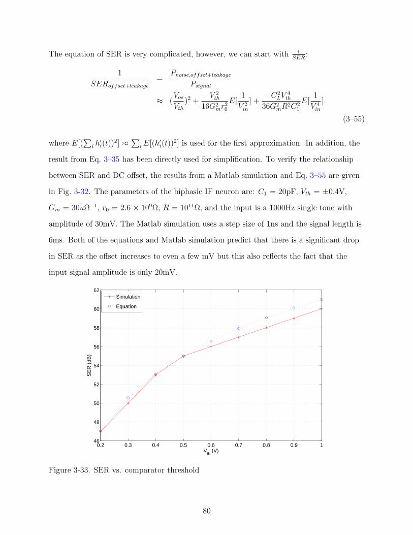
The equation of SER is very complicated, however, we can start with 1SER
:
1
SERoffset+leakage
=Pnoise,offset+leakage
Psignal
≈ (Vos
Vth
)2 +V 2
th
16G2mr2
0
E[1
V 2in
] +C2
LV 4th
36G2mR2C2
1
E[1
V 4in
]
(3–55)
where E[(∑
i h′i(t))
2] ≈ ∑i E[(h′i(t))
2] is used for the first approximation. In addition, the
result from Eq. 3–35 has been directly used for simplification. To verify the relationship
between SER and DC offset, the results from a Matlab simulation and Eq. 3–55 are given
in Fig. 3-32. The parameters of the biphasic IF neuron are: C1 = 20pF, Vth = ±0.4V,
Gm = 30uΩ−1, r0 = 2.6 × 10⁹Ω, R = 1011Ω, and the input is a 1000Hz single tone with
amplitude of 30mV. The Matlab simulation uses a step size of 1ns and the signal length is
6ms. Both of the equations and Matlab simulation predict that there is a significant drop
in SER as the offset increases to even a few mV but this also reflects the fact that the
input signal amplitude is only 20mV.
0.2 0.3 0.4 0.5 0.6 0.7 0.8 0.9 146
48
50
52
54
56
58
60
62
Vth
(V)
SE
R (
dB)
Simulation
Equation
Figure 3-33. SER vs. comparator threshold
80

The results about how SER changes with increasing threshold from Eq. 3–55 and
Matlab simulation are given in Fig. 3-33. The simulation parameters are similar to what
are used in Fig. 3-32 except that the DC offset is set to 5mV. Both of the two curves
predict that when the threshold increases, the SER also increases.
2000 3000 4000 5000 6000 7000 8000 9000 1000052
53
54
55
56
57
58
Frequency (Hz)
SE
R (
dB)
Figure 3-34. SER vs. input single tone frequency
Another simulation is done to display the relationship between SER and input single
tone frequency with 5mV DC offset. Fig. 3-34 tells us that the SER is independent of the
single tone frequency. This simulation result matches with the real testing results as shown
in Fig. 3-18.
Eq. 3–55 shows that SER is dependent on many factors, for example, the “pseudo-
resistor” introduced DC offset and some other circuit factors. Since the relationship
between SER and the circuit factors has been discussed in the precious subsections, it may
be insightful if we just focus on the relationship between SER and the DC offset. We can
81

simplify Eq. 3–53 as
Pnoise,offset = E[(Vin(t)− Vin(t))2]
=1
G2m
E[(∑
i
h′i(t)(θi − θ))2]
=1
G2m
E[(∑
i
(h′i(t))2)]E[(θi − θ)2]
=C2
L
G2m
E[(∑
i
(h′i(t))2)]E[(Vthi − Vth)
2]
=C2
L
G2m
E[(∑
i
(h′i(t))2)]E[(Vos)
2] (3–56)
here the noise introduced by the leakage is ignored. The power of the signal is still the
same as Eq. 3–54. The resulting SER can be derived as follows:
SERoffset =Psignal
Pnoise,offset
≈ E[V 2th]
E[V 2os]
≈ (Vth
Vos
)2 (3–57)
While this approximation can not provide accurate values of SER, it clearly shows how
the DC offset affects the reconstructed SER. From this equation, it is clear that when the
offset is reduced or the threshold is increased, the SER can be increased.
82

CHAPTER 4EIGHT-CHANNEL BIPHASIC INTEGRATE-AND-FIRE WITH ADDRESS EVENT
REPRESENTATION READOUT
4.1 Introduction
The biphasic spike representation circuit has been described in the previous chapter
as a single-channel system. Each system has two pulse output channels: one for positive
spikes and one for negative spikes. When several such systems are put in a single chip
to simultaneously record the multichannel neural signal activity, the required number of
dedicated output wires increases. In order to reduce the connection wires and make use
of the communication channel, the Address Event Representation (AER) protocol is used
to multiplex several pulse output channels. In this multiplexing scheme, an asynchronous
digital arbiter monitors the output of all the integrate-and-fire neurons. In the proposed
circuits, a 4-bit address will encode the 8 channel neurons since each channel has both of
positive and negative spikes. Once the 4-bit address is generated by the AER protocol,
it can be further modulated onto a single channel for wireless transmission. There are
many possible modulation schemes such as frequency modulation or width modulation.
Frequency modulation requires an oscillator, which increases the circuit complexity. With
width modulation, the address can be encoded with the appropriate pulse width or the
time between two pulses. This mechanism ensures that extremely simple and low power
hardware be used.
A variation of the AER protocol has been successfully employed in the time-to-first-
pulse imager chip designed within the CNEL lab [25, 26, 27]. In the time-to-first-pulse
imager chip, an asynchronous digital arbiter is used to scan off the address buses of
all the pixels. Once a pixel generates a spike, a request signal is sent to the arbiter.
Upon acknowledgement, the address or the corresponding pixel can be transmitted. The
drawback of this AER protocol arises when two or more pulses fire at nearly the same
time. In this case, the AER structure will just transmit one of the pulses while the other
83

pulse is buffered. By doing this, this delay will change the firing times of the pulses. With
fast digital electronics, this latency can be made small enough for most applications.
Vth+-
+
+
-
Vth-
M1 C
Vmid
Reset
Iin
Ro
w In
terf
ace
Ro
w A
rbite
r
Row
Ad
dre
ss E
ncoder
Throughput control
Column Arbiter
Column Address Encoder
Latches Latch Control
Row_request~
Digital
Block
Co
l_re
qu
est(
n)~
Co
l_re
qu
est(
n+
1)~
Row_sel
Reset
8 channel
4 4 neuron array
I/O
I/O
Figure 4-1. Block diagram of the 8-channel address-event-representation (AER) recordingsystem
The block diagram of an 8-channel recording system is shown in Fig. 4-1. 8 channels
of the biphasic spike generator are arranged as a 4 × 4 neuron array. To facilitate the
layout, both positive and negative spike outputs of each neuron are arranged in the
same row but in different column. One should bear in mind that this arrangement is not
optimal in terms of transmission speed, because a maximum of 2 neurons in each row can
generate the spikes at the same time. On the other hand, if all positive spikes are arranged
in two rows while all negative spikes are put in another two rows, and when all neurons in
the same row generate the spikes at the same time, then just one row address needs to be
transmitted. This system operates as follows:
84

1. Integrate and row request: After reset, each neuron begins to integrate the current.Once the voltage over the capacitor (C) is across a threshold, a correspondingpositive or negative spike is generated. The Row request∼ line is pulled down to senda row request.
2. Row select and column request: The row arbiter selects a row from the spiking rowsby making corresponding Row sel high and the selected row address is stored andencoded by the row address encoder. After the Row sel is received, all the spikingneurons in that row can send out column requests by pulling down Col request∼.In this 8-channel system, 2 columns at maximum can send this request signalsimulantaneously.
3. Column select and reset: The column latch records all column requests of thecurrently firing neruons in the selected row. Once this is done, two steps are takenat the same time: 1. the column arbiter begins to encode the column address; 2.the latched neurons in that row are all reset and they can begin to integrate again;the reseted neurons will therefore widthdraw the corresponding row request signal.Subsequently, the other valid Row request∼ can be processed by the row arbiter,while the row interface citcuit still blocks a new Row sel from being issued untilall latched neurons have been processed by the column arbiter and column addressencoder.
In the following section, the clocked AER circuit scheme will be described in detail.
Accurate spike timing is crucial for signal reconstruction. The primary drawback of the
AER protocol is the potential timing jitter or even spike loss, which adds distortion to the
reconstructed signal. These imperfections will also be addressed in this chapter.
4.2 Address Event Representation Structure
AER is an asynchronous readout scheme implemented with digital circuits. Unlike
other digital circuits, the asynchronous AER structure is difficult to simulate with
standard Verilog or VHDL languages. Instead, CADENCE SpectreS is used as the
simulator in this design. The digital asynchronous readout circuit mainly consists of a row
arbiter tree, a column arbiter tree, a column latch, a column latch control, a row interface
and a throughput control block. The throughput block has already been successfully
employed in the time-to-first-pulse imager chip within the CNEL lab [25, 26, 27].
Most of the detailed circuits of the AER protocol were originally designed by Boahen
[28]. For the reader’s convenience, they are briefly described in this section.
85

4.2.1 Arbiter
The arbiter cell shown in Fig. 4-2 is the basic unit for the row arbiter tree and column
arbiter tree. This arbiter circuit was originally used by Boahen [28]. An arbiter tree is
built from two-input arbiter cells using a binary tree architecture.
NAND
NAND
NA
ND
NA
ND
Req_in_1
Req_in_2
Sel_out_1~
Sel_out_2~
Sel_in~
VD
D
Req_out
Req_
in_1
Req_in
_2
Sel_
in~
Req_out
Req_out
Figure 4-2. Schematic of the arbiter cell
Each arbiter cell has two lower ports and one upper port. Each lower port has one
request input (Req in) and select output (Sel out∼). The upper port has one request
output (Req out) and one select input (Sel in∼). Whenever one or two lower active-high
ports, Req in 1 and Req in 2, makes a request, the arbiter cell relays the request signal
to the upper level by making Req out high. Once the current arbiter request to the upper
level is acknowledged, i.e., Sel in∼=0, the acknowledgment signal will be relayed to one of
the lower ports by zeroing Sel out 1∼ or Sel out 2∼. For example, if just one port sends
the request, then this port will be granted with the acknowledgment; however, if both
ports make the request at the same time, then just one of them can be granted with the
acknowledgment depending on the competition. Only when both lower input ports reset
their request signals, i.e., Req in 1 = 0 and Req in 2 = 0, the request to the upper level
can be reset to zero. In this case, even just one lower input can be selected when both sent
the request, the unselected port will be serviced closely following the previously selected
86

one. This property can speed up the arbiter tree when many channel are frequently active
[28].
4.2.2 Row Interface
The row interface shown in Fig. 4-3 is used to control whether a row can be selected
by the row arbiter [28]. There is one row interface circuit for each row. Only when the
Row sel en signal from the latch control circuit is enabled, the select signal Arbiter sel∼
from the arbiter can be transferred to the row select signal Row sel.
Row_sel
VDD
Row_request~ Arbiter_request
Arbiter_sel~
Row_sel_en
Figure 4-3. Schematic of the row interface
4.2.3 Latch and Latch Control
The latch and latch control circuits shown in Fig. 4-4 are used to increase the
throughput of the asynchronous readout [28]. Each column has one latch cell and the
whole array has just one latch control block. The important control signals include:
• cox∼ is the request signal, shared by all the neurons in the same column.
• b is used to control whether the request signals from cox∼ are allowed to enter thelatch cells.
• lp monitors whether there is request signal on the cox∼.
• g∼ indicates whether there is still valid data inside the latch cells.
• Col request n is the column request signal going to the column arbiter.
87

VDD
VDD
VDD
RES~
g~
Col_sel_n
Col_request_n
lp
Cox~
b
(a)
VDD
VDD
VDD
lp
b
Row_sel_enLatch_data_ready
Row_address_trigger
g~
(b)
Figure 4-4. Schematics of the latch cell and latch control: (a) latch cell; (b) latch control.
• Col sel n is the column acknowledgment signal from the column arbiter.
• Row sel en goes to the row interface (see Fig. 4-3), which enables the new rowselection signal going into the neuron array.
• latch data ready is valid after request on cox∼ have already entered the latch cell.This signal, together with row sel, reset the neuron which have fired in the selectedrow.
• row address trigger triggers the row address encoder to update the row address.
One thing need to keep in mind is that signal b, lp and g∼ are shared by all latch
cells.
88

The operations of latch and latch control are described as below: Initially, Cox∼ = 1
and reset signal makes RES∼ = 0, which further makes Col request = 0. Then we have
Col sel = 0, g∼ = 1, lp = 0, b = 1, Row sel en = 1 and Latch data ready = 1.
Once a row sends a request to the row arbiter, with Row sel en = 1, the select signal
from the row arbiter can reach the neuron unit and Row sel = 1 (see Fig. 4-3). Then
the neuron unit can send the column request signal by making Cox∼ = 0 and pushing
up lp. Since b = 1 at this time, Cox∼ = 0 can go ahead to send a request signal to the
column arbiter by making Col request = 1, which further pulls down g∼. The change of
g∼ and lp lead to b = 0 which stops all the incoming column requests. Simultaneously,
Row sel en = 0 disables the row interface functions and guarantees no new row select
is granted. At the same time, the active Latch data ready and Row sel reset all spiking
neurons in the selected row, which further disables the column request signal Cox∼. In
addition, Row address trigger triggers the row address update.
In ideal situation, all the spikes output will be transmitted, with or without a delay.
However, spike loss can happen in the real chip test. Before we explain how spike drop
happens, let’s take a look at how the spike get transferred. When there is a spike get
generated, it first sends the row request signal to the row arbiter. When the row request
signal is acknowledged, the column indexes of all the neurons that are spiking in the same
row will be saved in a buffer. After that, a row reset signal will be combined with the
spike output (an AND gate is used) to reset all the spiking neurons from the same row.
Which means that if this neuron within this row is having a spike output, the row reset
signal can take effect to this neuron and reset it; however, if this neuron is not generating
a spike output, the row reset signal does not have any effect on this neuron. After this
reset process, these neurons with spike outputs can begin another new integration period.
If there are two neurons (A and B) from the same row generate spikes one after another,
and the first neuron A sends the row request signal while the second neuron B is still
integrating. When the row request signal is acknowledged, the buffer begins to record
89

the column index of the spiking neurons (at this time, just neuron A is recorded because
neuron B does not generates spike yet). When the buffer finishes the recording and
the row reset signal begins to reset neuron A, neuron B just generates a spike. In this
occasion, because both A and B have spike outputs, the row reset signal reset both of
them. The result is that neuron B will begin a new integration period while its previous
spike gets dropped.
After each column is serviced, the corresponding Col sel will be set to one which,
with the aid of b = 0, can remove the column request by making Col request = 0. With
the removal of the column request signal, Col sel will also be reset to zero. When all the
column request signals are processed, all Col request and Col sel are set to zero, which
makes g∼ = 1. When all spiking neurons are reset, Cox∼ = 1, which makes lp = 1. Both
lp = 1 and g∼ = 1 reset all the control signals back to their initial conditions, and all the
latch cells are ready for upcoming row and column requests.
4.2.4 Throughput Control
Col_arbiter_sel
~
1 1
~
2 2
RES
Col_encoder_in
Col_sel
Figure 4-5. Schematic of the throughput control block for clocked AER
The throughput control block shown in Fig. 4-5 was first introduced by Guo [27] to
simplify the chip testing. With the aid of two nonoverlapping clocks, this readout system
90

can achieve a speed above 50MHz [26]. The signal Col arbiter sel comes from the column
arbiter, the signal Col sel goes to the latch cell, and the signal Col encoder in triggers
the column address encoder. To facilitate the chip testing, this circuit is also used in the
eight-channel biphasic IF chip.
4.3 Chip Layout
Figure 4-6. Chip layout of the 8-channel biphasic IF neuron with AER readout
The layout of this chip with pads is shown in Fig. 4-6. There are eight channels of
biphasic IF neurons and each channel includes three components: the gm amplifier, the
comparators and the digital control block. The same blocks from all eight channels share
the same power supply and the AER circuit uses the digital control block power supply.
There are total three power supplies. Bypass capacitor is put as much as possible to
91

improve the performance. Guard rings are also used to eliminate the kick back noise from
the digital circuit. The total layout area including the pads is 9mm2.
4.4 Measurement Results
An eight-channel biphasic integrate and fire (IF) neuron chip with clocked AER
readout circuit has been fabricated using the AMI 0.6um process with a DIP40 package.
The single channel circuit has been described in the precious chapter. Since the time
required by the Cadence simulator to simulate the AER chip is very long (greater than
one week for a 1ms transient simulation), no simulation results are provided. However, this
eight-channel chip has been successfully tested.
4.4.1 One-Channel Input
We are very curious how the AER readout circuit affects the reconstructed signal’s
SER. The first measurement was conducted to answer this question. Two Agilent 33220A
signal generators were used in the testing. In this test setup, just one channel of the eight
channels was coupled to the output from one signal generator and all the inputs of the
other seven channels were grounded. Another Agilent 33220A signal generator was used
to generate the required clock for the throughput control block. The generated biphasic
spikes are modulated by the AER circuit and the final chip outputs are four bits of
address codes. An Agilent 1693A logic analyzer was used to record the four bits of address
information and this logic analyzer operated in the asynchronous mode with a sampling
rate of 5ns. With this setup, the only difference between this chosen channel and the
single channel chip is that the channel in the AER chip has the AER readout circuit while
the single channel chip has the spike output directly coupled to the logic analyzer. It is
apparent that the chosen channel in the AER chip should have lower reconstruction SER
than that from the single chip of biphasic IF neuron. There are two factors responsible
for the SER difference. First, there is a time delay introduced by the AER circuit, and
each generated pulse needs to wait for some time before it can be modulated into the final
four-bit address code, while in the case of single channel chip, each generated spike can
92

be directly read out by the logic analyzer. Second, the control clock for the throughput
control block also introduces some error. The applied maximum clock frequency was
10MHz, with the period of 100ns, while the logic analyzer worked with a 5ns sampling
rate. Therefore, the time resolution for the AER chip is larger than 100ns.
105
106
107
20
25
30
35
40
45
Frequency (Hz)
SE
R (
dB)
Figure 4-7. Clock frequency vs. SER (one channel)
The measurement result of one channel test is given in Fig. 4-7. In this testing, the
input of the chosen channel is set to a 1000Hz single tone with amplitude of 40mV peak-
to-peak, and the threshold of the comparator was set to ±0.4V. The readout clock was
swept from 100KHz to 4MHz. After the logic analyzer captured the four-bit address code,
a Matlab program was run to restore the corresponding biphasic pulse. The close-form
algorithm was used to reconstruct the single tone signal, and the fitting algorithm used
in the previous chapter was used to calculate the SER. Each SER is calculated based on
two periods of the reconstructed signal. From this figure, it is clear that the reconstructed
signal SER mostly ranges from 35dB to 45dB with the maximum SER of around 43dB
corresponding to a readout clock of 1MHz and 3MHz. This figure does not give a clear
93

relationship between the readout clock frequency and the reconstructed SER, however,
one observation is that the readout frequency corresponding to above 40dB is greater
or equal to 0.9MHz. From the single channel chip measurement result in Fig. 3-18, the
reconstructed SER with the same input signal and ±0.4V threshold is 45dB. Fig. 3-22
indicates that when the threshold increases, the SER is reduced. Based on this data,
the AER circuit with proper readout clock introduces very little error, and this error
contributes to this SER gap between 45dB and 43dB. When the clock frequency is too
slow, the SER might be restricted by the low readout throughput rate and poor time
domain resolution. When the frequency is too high, it is very likely that the fast clock
transition will introduce some noise inside the chip package, and this noise can reduce
the reconstructed SER. Therefore, there is a tradeoff when we decide which readout clock
frequency to choose.
105
106
107
2
3
4
5
6
7
8x 10
4
Frequency (Hz)
Spi
ke r
ate
(Pul
se/s
)
Figure 4-8. Clock frequency vs. output spike rate (one channel)
94

Figure 4-8 shows the readout spike frequency and corresponding output spike rate.
When the clock frequency is low, it is clear that the spike rate is increasing with faster
readout clock. This relationship is reasonable, because higher readout frequency means
larger throughput. In the readout process, when a spike is generated, it sends the request
for modulation. Only when this spike is read out, this neuron can integrate for the next
spike. Only one spike can be sent out during each clock period. When the clock frequency
is high, the generated spike can be quickly sent out, the new integration period can be
initiated sooner, and the spike rate is higher. On the other hand, if the clock frequency
is low, the neuron has to wait for a longer time before it can start another integration,
and the spike rate is lower. However, when the readout frequency is higher than 1MHz,
the spike rate is reduced even though the readout clock frequency is increasing. The
possible explanation is that when the clock frequency is too high, it injects more noise into
the chip substrate. This noise affects this system, for example, this noise can make the
“pseudo-resistor” introduced DC offset more unpredictable.
0 0.2 0.4 0.6 0.8 1 1.2 1.4 1.6 1.8 2−40
0
40
Am
plitu
de (
mV
)
(a)
0 0.2 0.4 0.6 0.8 1 1.2 1.4 1.6 1.8 2−1
0
1
Time (ms)
Am
plitu
de (
mV
)
(b)
FittedReconstructed
Figure 4-9. Measured reconstruction time domain result example: (a) Reconstructed sin-gle tone signal (red) and the 4-parameter fitted single tone signal (blue); (b)Error.
Fig. 4-9 shows an example of the offline reconstructed signal based on the AER chip
measurement. The input signal is a 1KHz sine wave with 40mV peak-to-peak amplitude.
95

The red curve Fig. 4-9 (a) is the reconstructed sine wave and the blue curve is the 4-
parameter fitting sine wave. Fig. 4-9 (b) is the error between the reconstructed signal
and the fitting signal. This reconstructed signal has 35dB SER and the corresponding
readout control clock frequency is 1.1MHz. One strange observation from this figure is
that the large error between the reconstructed signal and the fitting signal always happens
at the high signal amplitude region, this suggests that the delayed spike readout process is
responsible for this error.
4.4.2 Two-Channel Input
In the two-channel input measurement setup, we make two of the eight channels
to share the same input from one Agilent 33220A signal generator, and the inputs of
all the other six channels are grounded. Another Agilent 33220A was again used to
generate the readout clock. This measurement setup is actually the worst case for the two
channels since spikes are likely to occur at exactly the same time. If there is some phase
delay between these two inputs, for example, when the input of one channel hit the peak
amplitude, this channel will generate the densest pulse train; if at the same time, the input
of the second channel has the amplitude of zero, and the second channel will not generate
any spike. If this is the case, all the AER sources will be automatically assigned to the
first channel. Virtually, this two channel case equals the one channel case.
The setup we used was the worst case. When the input has the maximum amplitude,
both channels are generating the densest spike train, and both will compete to use the
AER readout circuit to send out the spikes. In this case, some of the output spikes have
to be delayed or even lost. Therefore, the reconstructed signals from this setup will be
lower. On the other hand, when the input has an input amplitude of zero, there will be
no spike from either channel, and the AER readout circuit will be wasted. In fact, in real
application, the two channels will have their individual input, and there will be always
some difference between the two inputs.
96

105
106
15
20
25
30
35
Frequency (Hz)
SE
R (
dB)
Figure 4-10. Clock frequency vs. SER (two channels)
The measurement result of two channels testing is given in Fig. 4-10. In this testing,
the output from the Agilent 33220A signal generator is set to a 1000Hz single tone with
amplitude of 40mV peak-to-peak, and the threshold of the comparator was set to ±0.4V.
The readout clock was swept from 100KHz to 4MHz. After the logic analyzer captured
the four-bit address code, a Matlab program was run to restore the corresponding biphasic
pulse. The close-form algorithm was used to reconstruct the single tone signal, and the
fitting algorithm was used to calculate the SER. Each SER is calculated based on two
periods of reconstructed signal, and the plotted SER is the average SER between these
two channels over the same time period. From this figure, it is clear that the reconstructed
signal average SER mostly ranges from 30dB to 35dB with the maximum SER of around
37dB corresponding to readout clock of 400KHz.
Fig. 4-11 shows the readout spike frequency and corresponding average output spike
rate over the two channels. When the clock frequency is low, it is clear that the spike rate
is increasing with faster readout clock. This trend is similar to that in the one channel
97

105
106
1
2
3
4
5
6
x 104
Frequency (Hz)
Spi
ke r
ate
(Pul
se/s
)
Figure 4-11. Clock frequency vs. output spike rate (two channels)
case (see Fig. 4-8). However, when the readout frequency is higher than 1MHz, the spike
rate is reduced even though the readout clock frequency is increasing. Surprisingly, this
trend is also similar to that happened in the one-channel case (see Fig. 4-8). Compared
to Fig. 4-8, the spike rates in the two-channel case are normally less than those in the
one-channel case. For example, the maximum spike rate in the one-channel case is 80K
pulse per second, while the maximum in the two-channel case is around 70K pulse/s.
Fig. 4-12 shows the measured time domain example from the above two-channel
setup. The reconstructed signal and the fitted signal from the first channel is shown in
Fig. 4-12 (a) and the corresponding SER is 43dB. Fig. 4-12 (b) gives the reconstructed
signal and the fitted signal from the second channel and the SER is 30dB. The errors
between the reconstructed signal and the fitted signal are shown in Fig. 4-12 (c) with the
red one corresponding to channel one and the blue one corresponding to channel two. This
measurement results correspond to the 400KHz readout clock frequency. Compared to the
98

0 0.2 0.4 0.6 0.8 1 1.2 1.4 1.6 1.8 2−20
0
20
40
Am
plitu
de (
mV
)
( a )
0 0.2 0.4 0.6 0.8 1 1.2 1.4 1.6 1.8 2−4
−2
0
2
Time (ms)
Am
plitu
de (
mV
)
( c )
0 0.2 0.4 0.6 0.8 1 1.2 1.4 1.6 1.8 2−20
0
20
40
Am
plitu
de (
mV
)
( b )
Reconstructed
Fitted
Panel a error
Panel b error
Reconstructed
Fitted
Figure 4-12. Measured reconstruction time domain result example: (a) Reconstructedsingle tone signal (red) and the 4-parameter fitted single tone signal (blue)from the first channel; (b) Reconstructed single tone signal (red) and the 4-parameter fitted single tone signal (blue) from the second channel; (c) Errorfrom the first channel (red) and from the second channel (blue).
results shown in Fig. 4-7, we can find that the first channel’s SER (43dB) is almost equal
to the maximum SER achieved in one channel case. However, the SER from the second
channel is much worse than that from the first channel. This result does not mean that
the reconstructed signal from the first channel is always better than that from the second
channel. In fact, sometime the signal from the second channel has a higher SER than that
of channel one.
4.4.3 Three-Channel Input
In the three-channel input measurement setup, all three chosen channel shared the
same input: 1000Hz single tone with 40mV peak-to-peak amplitude. One Agilent 33220A
signal generator was used to provide this single tone. Another Agilent 33220A was used
to generate the readout clock and the clock frequency was swept from 100KHz to 4MHz.
99

Since all three channels share the exactly same input, this is the worst case in the three-
channel setup. The threshold of the biphasic IF comparators were set to ±0.4V. The
measurement are based on 2ms time period.
105
106
12
14
16
18
20
22
24
26
28
30
32
Frequency (Hz)
SE
R (
dB)
Figure 4-13. Clock frequency vs. SER (three channels)
The measurement result of three channels testing is given in Fig. 4-13. The shown
SER is the averaged SER over the three channels during the same 2ms period. From this
figure, it is clear that the reconstructed signal average SER mostly ranges from 26dB to
32dB with the maximum SER of around 32dB corresponding to readout clock of 200KHz
and 900KHz. The SER with the clock frequency lower than 1MHz is higher than that
corresponding to the frequency higher than 1MHz. Surprisingly, this observation also
applies to the two-channel case (see Fig. 4-10).
Fig. 4-14 shows the average spike rate corresponding to different readout clock
frequencies. Similar to those in the two-channel and one-channel cases, the spike rate first
increases with the faster clock and then drops when the clock frequency further increases.
100

105
106
1
2
3
4
5
6
7
x 104
Frequency (Hz)
Spi
ke r
ate
(Pul
ses/
s)
Figure 4-14. Clock frequency vs. output spike rate (three channels)
4.4.4 Four-Channel Input
In the four-channel input measurement setup, all the four channels shared the same
input: 1000Hz single tone with 40mV peak-to-peak amplitude. One Agilent 33220A
signal generator was used to provide this single tone. Another Agilent 33220A was used
to generate the readout clock and the clock frequency was swept from 200KHz to 4MHz.
The threshold of the biphasic IF comparators was set to ±0.4V and the measurement was
based on 2ms time period.
The measurement result of four channels testing is given in Fig. 4-15. The shown SER
is the averaged SER over the four channels during the same 2ms period. From this figure,
it is clear that the reconstructed signal average SER mostly ranges from 20dB to 32dB
with the maximum SER of around 32dB corresponding to readout clock of 2MHz. In this
figure, even when the clock frequency is higher than 1MHz, the SER does not drop. This
is different from the two-channel and three-channel cases. The reason is that when we
101

105
106
10
15
20
25
30
Frequency (Hz)
SE
R (
dB)
Figure 4-15. Clock frequency vs. SER (four channels)
have too many active channels, the improvement from the faster clock frequency or wider
communication bandwidth is more dominant than the noise introduced by the clock.
Fig. 4-16 shows the average spike rate corresponding to different readout clock
frequencies. Different from what we observe in the one-, two- and three-channel cases, we
find that the spike rate is always increasing with the increasing clock frequency. This trend
is consistent with the SER trend in four channels case: both of SER and spike rate does
not decrease when clock frequency is faster.
4.4.5 Eight-Channel Input
Finally, we have conducted the eight-channel testing. Similar to the previous four test
setups, one Agilent 33220A signal generator was used to provide a single tone to all the
eight channels. Another Agilent 33220A was used to generate the readout clock and the
clock frequency was swept from 400KHz to 4MHz. We have attempted to use the clock
frequency of less than 400KHz, however, no acceptable results were able to be achieved.
This is what we expected, because with for example 200KHz readout frequency, each
102

105
106
2
2.5
3
3.5
4
4.5
5
5.5
x 104
Frequency (Hz)
Spi
ke r
ate
(Pul
se/s
)
Figure 4-16. Clock frequency vs. output spike rate (four channels)
channel can be assigned up to 25KHz bandwidth, which is greatly below what we observed
in the previous testing. The thresholds of the biphasic IF comparators were set to ±0.4V
and the measurement were based on 2ms time period.
The measurement result of eight channels testing is given in Fig. 4-17. The average
SER over eight channels mostly ranges from 16dB to 28dB with the maximum SER of
around 28dB corresponding to readout clock of 3MHz. In this figure, even when the
clock frequency is higher than 1MHz, the SER does not drop, this is similar to what we
observed in the case of four channels and it is different from those in two channels and
three channels. The reason is the same as what we discussed in the previous section.
Fig. 4-18 shows the example of reconstructed signal (red) and the fitted signal (blue)
from all the eight channels. The corresponding readout clock frequency is 3MHz and the
average SER is around 28dB.
103
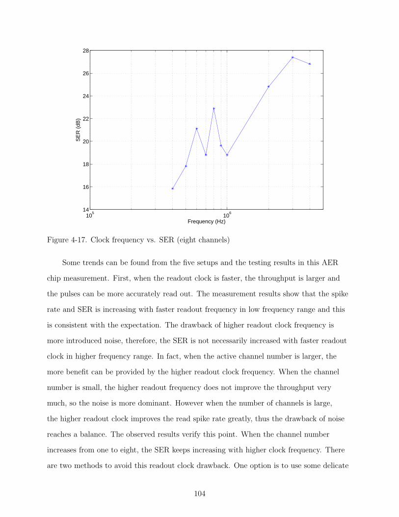
105
106
14
16
18
20
22
24
26
28
Frequency (Hz)
SE
R (
dB)
Figure 4-17. Clock frequency vs. SER (eight channels)
Some trends can be found from the five setups and the testing results in this AER
chip measurement. First, when the readout clock is faster, the throughput is larger and
the pulses can be more accurately read out. The measurement results show that the spike
rate and SER is increasing with faster readout frequency in low frequency range and this
is consistent with the expectation. The drawback of higher readout clock frequency is
more introduced noise, therefore, the SER is not necessarily increased with faster readout
clock in higher frequency range. In fact, when the active channel number is larger, the
more benefit can be provided by the higher readout clock frequency. When the channel
number is small, the higher readout frequency does not improve the throughput very
much, so the noise is more dominant. However when the number of channels is large,
the higher readout clock improves the read spike rate greatly, thus the drawback of noise
reaches a balance. The observed results verify this point. When the channel number
increases from one to eight, the SER keeps increasing with higher clock frequency. There
are two methods to avoid this readout clock drawback. One option is to use some delicate
104

0 0.5 1 1.5 2−20
0
20
Am
plitu
de (
mV
)
Channle 1
0 0.5 1 1.5 2−20
0
20
Am
plitu
de (
mV
)
Channle 2
0 0.5 1 1.5 2−20
0
20
Am
plitu
de (
mV
)
Channle 3
0 0.5 1 1.5 2−20
0
20
Am
plitu
de (
mV
)
Channle 4
0 0.5 1 1.5 2−20
0
20
Am
plitu
de (
mV
)
Channle 5
0 0.5 1 1.5 2−20
0
20
Am
plitu
de (
mV
)
Channle 6
0 0.5 1 1.5 2−20
0
20
Time (ms)
Am
plitu
de (
mV
)
Channle 7
0 0.5 1 1.5 2−20
0
20
Time (ms)
Am
plitu
de (
mV
)
Channle 8
Figure 4-18. Measured reconstruction time domain result example (red is the recon-structed single tone signal and the blue is the 4-parameter fitted single tonesignal)
layout to reduce the clock-introduced noise. Another option is to use a clock-free AER
circuit to read out these pulses.
Second, corresponding to the same readout clock frequency, the more channels are
active, the less average SER can be achieved, as shown in Table 4-1 (the first row in this
table comes from the single-channel chip measurement). This is obvious because when the
channel number is large, there is more possibility for the spikes to encounter collisions, get
delayed or even be dropped during the readout. The measurement results also verify this
point. Maybe some better readout circuit can avoid this problem.
4.5 Nonideal Issues
As we see in the chip measurement, there are some nonideal factors that affect the
testing results. With these nonideal factors, noise for example, the real limit of this circuit
design can not be achieved. We will discuss these nonideal issues in this section.
105

Table 4-1. Eight-channel chip measurement summary
Number of channels Maximum average SER (dB) Readout clock (Hz)
1(NonAER) 45 N/A1 43 1M2 37 400K3 31.5 900K4 31.5 2M8 27.5 3M
4.5.1 Timing Error Forced by the Readout Clock
The timing of the output spike must be digitized to be processed by a DSP. There
will be some error during this digitizing process, no matter whether a unidirectional IF
neuron or biphasic IF neuron is used. The error introduced by the normal timing jitter in
both cases has been discussed by Wei [15] and Chen [22]. In their cases, the timing jitter
refer to the error introduced by the recording device. This error source is still there in the
AER chip we just measured. In addition to this, however, there is a more severe timing
error due to the readout clock. In the case of one channel, when a spike is generated by
the neuron, it has to be processed by the AER readout part. To make things worse, this
spike can only be processed once per clock period. When a spike is recorded, the only
thing we know is that this spike was generated during the previous readout clock period.
The exact spike time is unknown. Since this timing uncertainty is on the order of 1µs, the
other timing jitter (mostly on the order of 1ns) can be ignored. Even though this timing
error is different from the timing jitter discussed by Wei and Chen, they work in the same
way to affect the reconstructed signal. Therefore, their conclusion will be directly cited
here.
Wei concluded that with the sampling frequency increasing, the SER of the recon-
structed signal will be improved [15]. This conclusion is very straightforward. To check
the validity of this conclusion in our case, some Matlab simulations are run. In this simu-
lation, an eight-channel biphasic IF neuron AER chip was considered. The parameters of
each neuron are the same as those used in the previous chapter (C1 = CL = 20pF, Vth =
106

105
106
107
108
30
40
50
60
70
80
Frequency (Hz)
SE
R (
dB)
Figure 4-19. Clock frequency vs. SER (one channel Matlab simulation)
±0.4V, Gm = 30uΩ−1, r0 = 2.6 × 10⁹Ω, R = 1011Ω). The Matlab simulation step is 1ns.
The input for one channel is a single tone of 1KHz with amplitude of 30mV. The input
signal lasts for 2ms. In the first simulation, just one channel IF neuron was active, and the
spike output had to pass the AER circuit. In this simulation, when there is a spike gets
generated, it has to be held until there is a readout clock rising edge. Then it is simplified
that this spike is transferred at the end of this clock period. Only after the previous spike
is read out, the next spike can begin the integration process. The readout clock frequency
was swept from 100KHz to 200MHz. The reconstructed SER is shown in Fig. 4-19. From
this simulation, it is clear that the SER is increasing from 35dB to 80dB when the readout
clock frequency increases from 100KHz to 200MHz. In the low clock frequency range, The
overall simulation SER is around 7dB higher than that of measurement result. Due to the
noise, the faster readout clock was not used in the measurement.
107
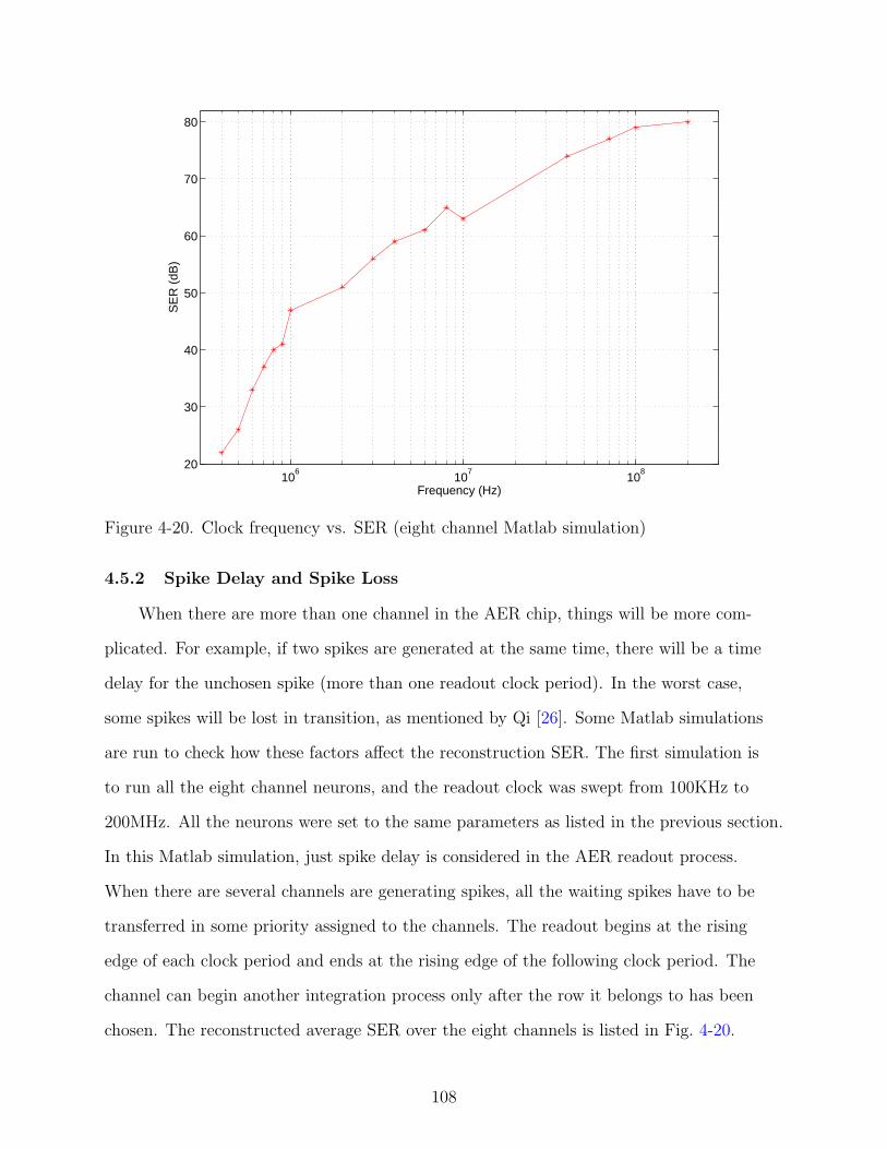
106
107
108
20
30
40
50
60
70
80
Frequency (Hz)
SE
R (
dB)
Figure 4-20. Clock frequency vs. SER (eight channel Matlab simulation)
4.5.2 Spike Delay and Spike Loss
When there are more than one channel in the AER chip, things will be more com-
plicated. For example, if two spikes are generated at the same time, there will be a time
delay for the unchosen spike (more than one readout clock period). In the worst case,
some spikes will be lost in transition, as mentioned by Qi [26]. Some Matlab simulations
are run to check how these factors affect the reconstruction SER. The first simulation is
to run all the eight channel neurons, and the readout clock was swept from 100KHz to
200MHz. All the neurons were set to the same parameters as listed in the previous section.
In this Matlab simulation, just spike delay is considered in the AER readout process.
When there are several channels are generating spikes, all the waiting spikes have to be
transferred in some priority assigned to the channels. The readout begins at the rising
edge of each clock period and ends at the rising edge of the following clock period. The
channel can begin another integration process only after the row it belongs to has been
chosen. The reconstructed average SER over the eight channels is listed in Fig. 4-20.
108
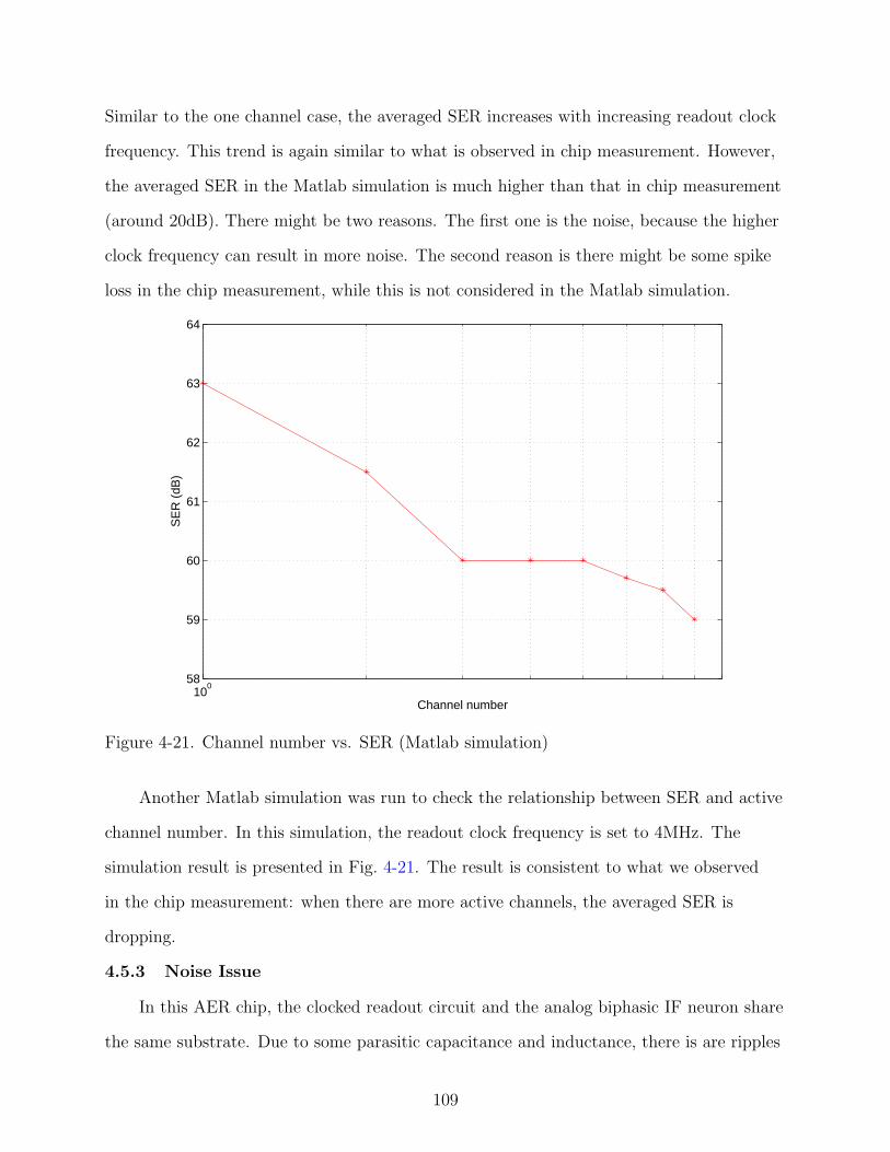
Similar to the one channel case, the averaged SER increases with increasing readout clock
frequency. This trend is again similar to what is observed in chip measurement. However,
the averaged SER in the Matlab simulation is much higher than that in chip measurement
(around 20dB). There might be two reasons. The first one is the noise, because the higher
clock frequency can result in more noise. The second reason is there might be some spike
loss in the chip measurement, while this is not considered in the Matlab simulation.
100
58
59
60
61
62
63
64
Channel number
SE
R (
dB)
Figure 4-21. Channel number vs. SER (Matlab simulation)
Another Matlab simulation was run to check the relationship between SER and active
channel number. In this simulation, the readout clock frequency is set to 4MHz. The
simulation result is presented in Fig. 4-21. The result is consistent to what we observed
in the chip measurement: when there are more active channels, the averaged SER is
dropping.
4.5.3 Noise Issue
In this AER chip, the clocked readout circuit and the analog biphasic IF neuron share
the same substrate. Due to some parasitic capacitance and inductance, there is are ripples
109

at each rising edge and each falling edge of each clock period. There are more ripples when
a higher-frequency readout clock is used. This may explain why we can not always expect
higher SER when we increase the readout clock frequency. Excluding the readout clock
introduced noise, there is noise associated with each generated spike output. When there
are more active channels, or when there are more output spikes, there will be more noise.
These noise can affect the operation of the biphasic IF neuron through the substrate
or through the ripples on the power line. They can also directly distort the input signal.
Considering the input signal has small amplitude, this distortion can be a big issue. A
guard ring can reduce the substrate noise. It is also wise to separate the analog circuits
from the digital output as far as possible. Both methods have been used in the test chip.
Another solution is to design more robust circuits with higher power rejection ratio. With
a higher power rejection ratio, the ripples on the power line will have less effect on the
circuit operation.
Another method to increase the circuit robustness is to design a differential-mode
input circuit. For example, if the circuit has a differential-mode input pair, the distortion
to the input signal can be greatly reduced. In this case, this distortion shows itself as a
common mode noise, which can be rejected by the differential input pair.
110
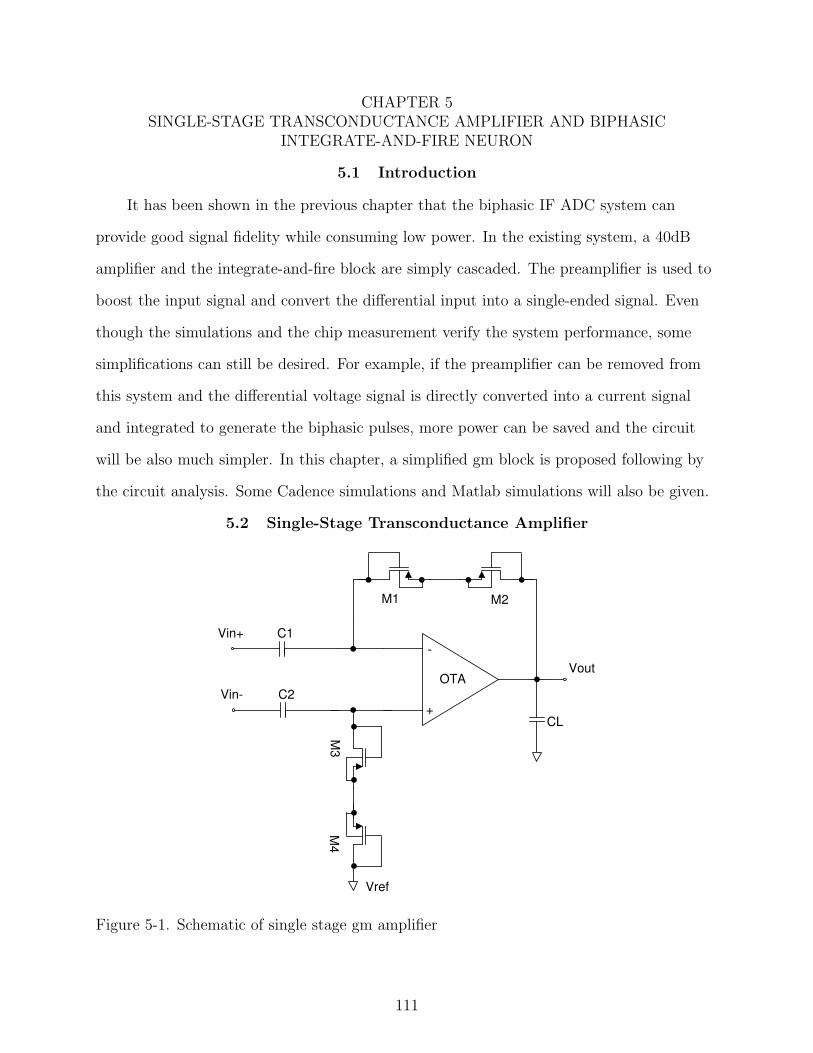
CHAPTER 5SINGLE-STAGE TRANSCONDUCTANCE AMPLIFIER AND BIPHASIC
INTEGRATE-AND-FIRE NEURON
5.1 Introduction
It has been shown in the previous chapter that the biphasic IF ADC system can
provide good signal fidelity while consuming low power. In the existing system, a 40dB
amplifier and the integrate-and-fire block are simply cascaded. The preamplifier is used to
boost the input signal and convert the differential input into a single-ended signal. Even
though the simulations and the chip measurement verify the system performance, some
simplifications can still be desired. For example, if the preamplifier can be removed from
this system and the differential voltage signal is directly converted into a current signal
and integrated to generate the biphasic pulses, more power can be saved and the circuit
will be also much simpler. In this chapter, a simplified gm block is proposed following by
the circuit analysis. Some Cadence simulations and Matlab simulations will also be given.
5.2 Single-Stage Transconductance Amplifier
Vin+
Vref
OTA
+
-
Vout
M2M1
C1
CL
Vin- C2
M4
M3
Figure 5-1. Schematic of single stage gm amplifier
111

Figure 5-1 shows the schematic of the new single stage gm amplifier, where M1
and M2, M3 and M4 are four diode-connected PMOS transistors. They act as “pseudo-
resistors” with resistance greater than 1011Ω. M1, M2 and C1 construct a high pass filter;
and M3, M4 and C2 also construct another high pass filter. Since these “pseudo-resistors”
have huge resistance, the cutoff frequency of these high pass filters are very low (less than
1Hz). Intuitively, this gm amplifier can be separated into two circuits. One of them is a
DC loop, which includes the four “pseudo-resistors” and the load capacitor CL. The DC
loop is actually a DC voltage follower, and the output DC voltage over CL is following the
voltage Vref . This DC loop is used to fix the DC operation point of this circuit. On the
other hand, when the AC loop is considered, the four “pseudo-resistors” can be ignored,
and this OTA works in open-loop with huge gain. In one word, this gm amplifier rejects
the DC component of the input signal and amplifies the AC component.
In the parameter configuration, the two input branches will be set to be identical so
that this gm amplifier will amplify only the differential-mode input signal. This is what we
desire for the neural signal application. Due to the DC drift, a reference signal is normally
used to cancel the DC drift in the neural signal [6].
Since the neural signal normally has the amplitude of 50–500 µV and the OTA will
has a DC offset of around 1mV, there is a concern about whether the DC offset will
suppress the interesting part of a neural signal. In fact, the DC offset will appear on the
load capacitor without being amplified while the neural signal will be boosted up by the
open-loop gain (normally 80dB). The result is the neural signal with the amplitude of
0.5–5V overlaps on the 5mV DC offset.
To better understand how this gm amplifier works, the transfer function is derived.
Similar to what we did in Chapter 3, the equivalent circuit of the gm amplifier is given
in Fig. 5-2 where r0 represents the output resistance of the OTA and Gm is the transcon-
ductance of the OTA. The circuit in this figure looks complicated, so we use superposition
method to solve this problem. First, we assume the input terminal Vin− is grounded. In
112
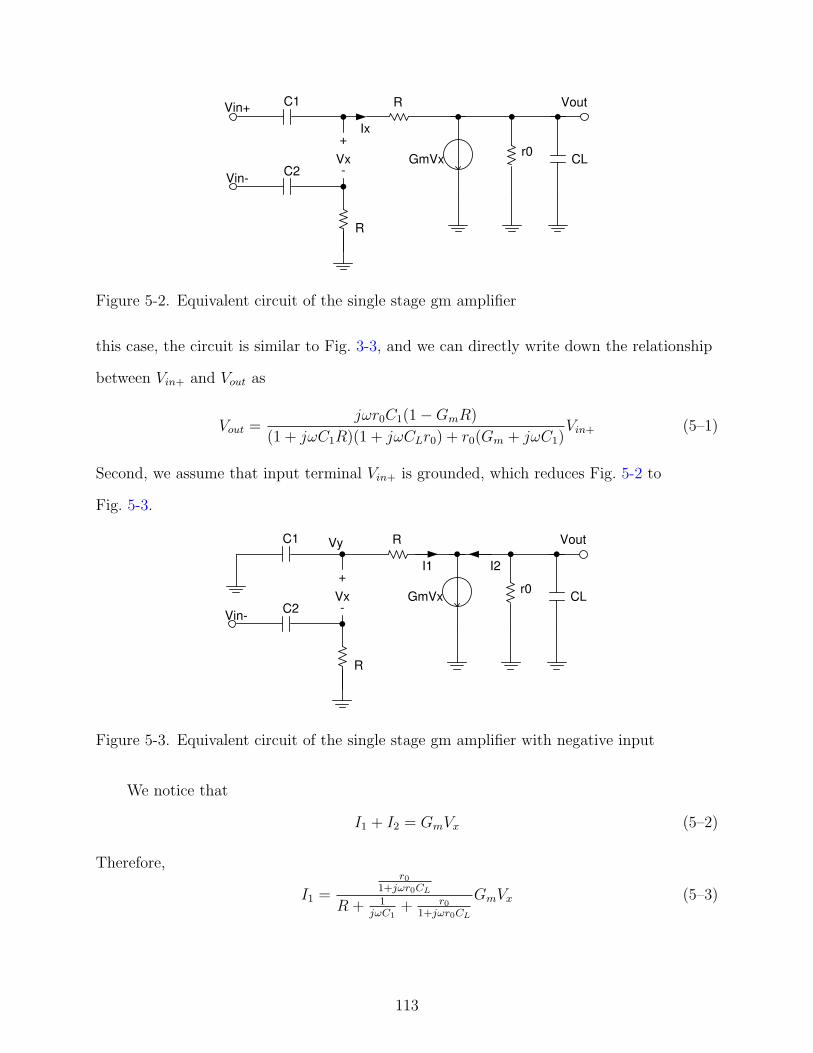
+
-
Vin+C1 VoutR
CLr0
GmVxVx
Ix
Vin-C2
R
Figure 5-2. Equivalent circuit of the single stage gm amplifier
this case, the circuit is similar to Fig. 3-3, and we can directly write down the relationship
between Vin+ and Vout as
Vout =jωr0C1(1−GmR)
(1 + jωC1R)(1 + jωCLr0) + r0(Gm + jωC1)Vin+ (5–1)
Second, we assume that input terminal Vin+ is grounded, which reduces Fig. 5-2 to
Fig. 5-3.
+
-
C1 VoutR
CLr0
GmVxVx
I1
Vin-C2
R
Vy
I2
Figure 5-3. Equivalent circuit of the single stage gm amplifier with negative input
We notice that
I1 + I2 = GmVx (5–2)
Therefore,
I1 =
r0
1+jωr0CL
R + 1jωC1
+ r0
1+jωr0CL
GmVx (5–3)
113

We also have
Vy = Vx +jωC2R
1 + jωC2RVin− (5–4)
Vy = − 1
jωC1
I1 (5–5)
and
Vout = Vy(1 + jωC1R) (5–6)
Combining Eq. 5–3 to Eq. 5–6, we can achieve the relationship between Vout and Vin−:
Vout =(1 + jωC1R)(jωC2R)
jωC2R
Gmr0
(1 + ωC1R)(1 + jωCLr0) + r0(Gm + jωC1)Vin− (5–7)
In practice, C1 is set equal to C2, which can simplify the above equation to
Vout =GmR(jωr0C1)
(1 + ωC1R)(1 + jωCLr0) + r0(Gm + jωC1)Vin− (5–8)
Comparing Eq. 5–8 to Eq. 5–1, we can find they are very similar. This makes sense,
because they are symmetrical in the circuit structure. Combine these two equations, the
final output can be written as
Vout = − GmR(jωr0C1)
(1 + ωC1R)(1 + jωCLr0) + r0(Gm + jωC1)(Vin+ − Vin−)
+jωr0C1
(1 + jωC1R)(1 + jωCLr0) + r0(Gm + jωC1)Vin+ (5–9)
It is clear from Eq. 5–9 that the output is amplified differential input overlapping with
a small signal proportional to Vin+. Apparently, the first term (amplified differential
signal) is what we desired in our application while the second is the noise. Fortunately,
the first term has a much higher gain than that of the second term. For example, if
Gm = 30×10−6Ω−1 and R = 1011Ω are used (there are the normal values used in the
circuit), the gain difference will be around 130dB. Therefore when the common-mode
signal and the differential-mode signal have comparable amplitude, the second term can
be ignored in the analysis without introducing much inaccuracy. Some detailed analysis
about this will be found in the following sections. If we separate Eq. 5–9 into two parts
114

with two transfer functions, both of them are two-pole and one-zero systems with exactly
the same zero and poles. The only difference will be a constant gain shift. Fig. 3-4 gave a
good example what the AC response looks like.
If we ignore the second item, and use Vin to represent Vin+ − Vin−, Eq. 5–9 can be
simplified to
Vout = − GmR(jωr0C1)
(1 + ωC1R)(1 + jωCLr0) + r0(Gm + jωC1)Vin (5–10)
This simplified equation is very similar to Eq. 3–22. If we review the derivation in Eq. 3–
23 again, we can find the following analysis results in Chapter 3 can be directly used here
because the transfer function in Eq. 3–22 was finally simplified to Eq. 5–10 to facilitate the
derivation. The SER equation in Eq. 3–35 can also be directly used in this application.
Even though there are many similarities between the single-stage gm amplifier and
the second-stage gm amplifier in Chapter 3, extra simulations are still necessary to find
the best parameters set. In the case of the second-stage gm amplifier, the input signal goes
from the output of the preamplifier where the differential neural signal is converted into
single-ended signal with being amplified by 40dB. If we consider that the neural signal has
an amplitude of 100µV, for example, the input signal for the second-stage gm amplifier
has the amplitude of around 10mV. In this occasion, moderate gain for second-stage
gm amplifier is good enough to generate enough pulses for reconstruction. In terms of
the single-stage gm amplifier, however, high gain is needed to boost the signal of 100µV
so that some pulses can be generated. There are several ways to increase the gain, for
example, we can decrease the load capacitor, we can also increase the transconductance
of the OTA. The simulation may give some clues about which way can be done to achieve
that.
One may argue that the gain does not need to be high if the threshold is reduced
properly. In Chapter 3, it is mentioned that the OTA input DC offset is around 5mV,
and this offset puts the first limit for the comparator threshold. The “pseudo-resistor”
115

introduced DC offset puts an even stricter limit for the threshold as we discussed in that
chapter. Therefore, reducing the thresholds can only be used to a limited extent.
If we take a further look at the noise term in Eq. 5–9, we may find that it is really
not a big problem. Recall in the case of second-stage gm amplifier, the input signal is the
output of the preamplifier [5]. The preamplifier has similar structure to the single-stage
gm amplifier so that the noise term was also included in the output of the preamplifier.
Based on this, it can be concluded that the noise (or the imperfection in differential
amplifier) is amplified and integrated in both gm amplifiers.
5.3 Simulation Results
5.3.1 Cadence Simulation
0 0.5 1 1.5 2 2.5−5
0
5
10x 10
−4
Am
plitu
de (
V)
(a)
0 0.5 1 1.5 2 2.5−1
−0.5
0
0.5
1
Time (ms)
Am
plitu
de
(b)
Vin+
Vin−
Figure 5-4. Simulated time domain example: (a) Two input signals; (b) Output spikes.
Connecting the single-stage gm amplifier to the digital block designed by Chen [5]
finishes the design of single-stage biphasic IF neuron using AMI 0.6µm technique. A
simulation was run in Cadence to verify the circuit analysis. In this circuit simulation, the
116

positive input is a superposition of five single tone: 2mV peak-to-peak 60Hz sine wave and
200µV peak-to-peak 100Hz, 500Hz, 1000Hz and 5000Hz sine waves. The negative input is
a 2mV peak-to-peak 60Hz single tone. The 60Hz signal in both inputs have the exactly
same phase, which is used to work as common-mode signal. The input capacitor of C1
and C2 were both set to 20pF and the integrator capacitor CL was set to 1pF. The OTA
in the second-stage gm amplifier (Chapter 3) is used here with the bias current of 8µA.
The thresholds of the comparators were set to ±0.08V. This transient simulation time was
set to almost 2.5ms. Fig. 5-4 shows the inputs and the spike output from this Cadence
simulation.
0 0.5 1 1.5 2 2.5−1
−0.5
0
0.5
Am
plitu
de (
V)
(a)
0 0.5 1 1.5 2 2.5−0.015
−0.01
−0.005
0
0.005
0.01
Time (ms)
Am
plitu
de (
V)
(b)
FittedReconstructed
Figure 5-5. Simulated time domain example: (a) Reconstructed signal (red) and fittedsignal (blue); (b) Error between the reconstructed signal and the fitted signal.
The generated spike train was read out and reconstructed by a Matlab program. To
evaluate this reconstructed signal, another artificial signal of superposition of four single
tones (100Hz, 500Hz, 1000Hz and 5000Hz) was generated. Here we assume the differential
amplifier removed the common mode signal of 60Hz sine wave and just the differential
117

mode signal got amplified. The reconstructed signal (red) and the generated fitted signal
(blue) are both normalized and given in Fig. 5-5 (a). The error between the reconstructed
signal and the fitted signal is also given in Fig. 5-5 (b). The results shown in Fig. 5-5 (a)
shows that the common mode signal is really removed and the amplified signal (or the
reconstructed signal) is composed mostly by the differential mode signal even though the
common-mode signal is much stronger than the differential-mode signal. This is exactly
what we expected.
5.3.2 Matlab Simulation
The above Cadence simulation has verified that this circuit is working as expected.
The transfer function derivation in the previous section has also shown that this circuit is
similar to the second-stage gm amplifier. However, due to different input signal amplitude
range and different input mode (differential input in the single-stage and single-ended
input in second-stage), some circuit parameters should also put different limits. This
makes it necessary to run some Matlab simulations to find the best circuit parameters for
maximizing the reconstructed signal’s fidelity.
The Matlab simulation uses the convolution between the inputs and the impulse
responses from the transfer function. To make the simulation more practical, the noise
term in Eq. 5–9 is also included in the simulation. Without special mention, all the circuit
parameters used in the following Matlab simulation are: C1 = C2 = 20pF, Vth = ±0.1V,
Gm = 30uΩ−1, r0 = 2.6 × 10⁹Ω, R = 1011Ω, CL = 1pF, and the input is a 1000Hz single
tone with 400µV peak-to-peak amplitude differential-mode signal superposing on a 600mV
peak-to-peak 60Hz common-mode sine wave.
The first simulation is to check how the DC shift can affect the reconstruction SER.
In this simulation, all the other parameters were fixed while the amplitude of the 60Hz
signal was swept from 0.01V to 300V. The reconstructed SER is shown in Fig. 5-6. From
this figure, it is clear that when the common-mode signal has an amplitude less than
or equal to 10V, the reconstructed signal will not be affected. Actually, the DC shift in
118

10−2
10−1
100
101
102
20
25
30
35
40
45
50
Amplitude (V)
SE
R (
dB)
Figure 5-6. SER vs. low frequency signal amplitude
neural signals is always less than 10V, therefore, this shift will not affect the real neural
signals.
The second simulation is run to find the best load capacitor for this gm amplifier. In
this simulation, all the other parameters were kept fixed while the load capacitance was
swept from 0.1pF to 10pF. The corresponding SER is given in Fig. 5-7. It is clear that
the SER drops with the increasing load capacitance. This is reasonable because when the
load capacitance is decreased, the output spike rate is rapidly increasing. One may wonder
why the maximum SER in this plot is around 60dB while the simulation result in Chapter
3 can be as high as 80dB. To explain this point, we may need to take another look at
Eq. 3–35, which is repeated here for the reader:
SERleakage ≈ 1V 2
th
16G2mr2
0E[ 1
V 2in
] +C2
LV 4th
36G2mR2C2
1E[ 1
V 4in
](5–11)
In the above equation, increasing input signal amplitude or reducing the load capacitance
can both increase the SER. Compared to reducing the load capacitor, increasing input
signal amplitude may be more efficient due to their different power function coefficients.
119
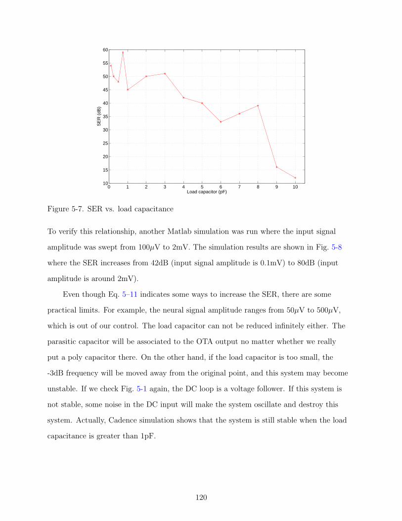
0 1 2 3 4 5 6 7 8 9 1010
15
20
25
30
35
40
45
50
55
60
Load capacitor (pF)
SE
R (
dB)
Figure 5-7. SER vs. load capacitance
To verify this relationship, another Matlab simulation was run where the input signal
amplitude was swept from 100µV to 2mV. The simulation results are shown in Fig. 5-8
where the SER increases from 42dB (input signal amplitude is 0.1mV) to 80dB (input
amplitude is around 2mV).
Even though Eq. 5–11 indicates some ways to increase the SER, there are some
practical limits. For example, the neural signal amplitude ranges from 50µV to 500µV,
which is out of our control. The load capacitor can not be reduced infinitely either. The
parasitic capacitor will be associated to the OTA output no matter whether we really
put a poly capacitor there. On the other hand, if the load capacitor is too small, the
-3dB frequency will be moved away from the original point, and this system may become
unstable. If we check Fig. 5-1 again, the DC loop is a voltage follower. If this system is
not stable, some noise in the DC input will make the system oscillate and destroy this
system. Actually, Cadence simulation shows that the system is still stable when the load
capacitance is greater than 1pF.
120

10−1
100
40
45
50
55
60
65
70
75
80
Amplitude (mV)
SE
R (
dB)
Figure 5-8. SER vs. input signal amplitude
Similar to what we did in Chapter 3, the bypass resistance R and the input capaci-
tance C were also swept to check the relationship between these parameters and the re-
construction SER. The simulation results are shown in Fig. 5-9 and Fig. 5-10 respectively.
It is clear from Fig. 5-9 that the SER increases with the increasing input capacitance.
However, finite layout area prevents us from using a huge capacitor. A 20pF-capacitor was
used in the chip design. Fig. 5-10 shows that the SER increases with the increasing bypass
resistance. In the first-stage gm amplifier, since the voltage across the “pseudo-resistor” is
around 0.1V (compared to 0.4V in the second-stage gm amplifier), the bypass resistance
should be a little bit higher than that in the second-stage case.
Comparing all the simulation results from Fig. 5-7 to Fig. 5-10, it can be found that
for a wide range of input capacitance, output capacitance and bypass resistance, the SER
of reconstructed signal is always below 60dB. However, when the input signal amplitude is
increased above 500µV, the SER rises above 60dB. When the amplitude increases to 2mV,
the SER is around 80dB. Therefore, it can be concluded that the input signal amplitude is
an important reason to the lower SER achieved in the first-stage gm amplifier.
121
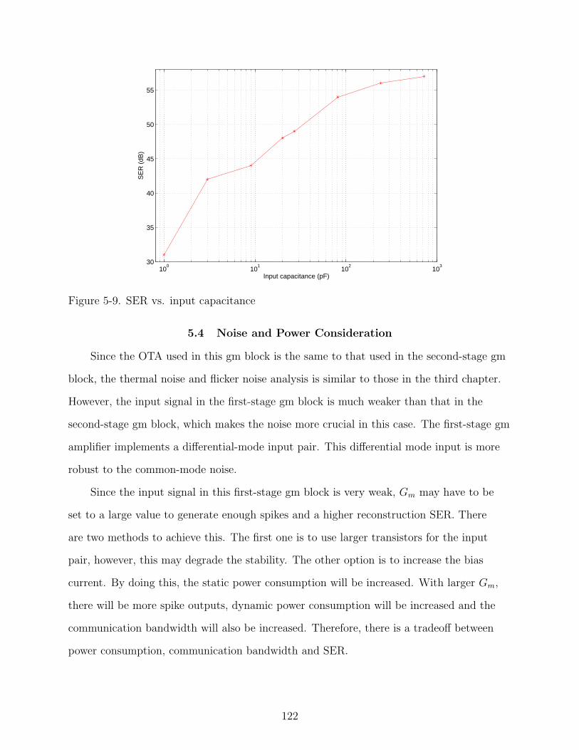
100
101
102
103
30
35
40
45
50
55
Input capacitance (pF)
SE
R (
dB)
Figure 5-9. SER vs. input capacitance
5.4 Noise and Power Consideration
Since the OTA used in this gm block is the same to that used in the second-stage gm
block, the thermal noise and flicker noise analysis is similar to those in the third chapter.
However, the input signal in the first-stage gm block is much weaker than that in the
second-stage gm block, which makes the noise more crucial in this case. The first-stage gm
amplifier implements a differential-mode input pair. This differential mode input is more
robust to the common-mode noise.
Since the input signal in this first-stage gm block is very weak, Gm may have to be
set to a large value to generate enough spikes and a higher reconstruction SER. There
are two methods to achieve this. The first one is to use larger transistors for the input
pair, however, this may degrade the stability. The other option is to increase the bias
current. By doing this, the static power consumption will be increased. With larger Gm,
there will be more spike outputs, dynamic power consumption will be increased and the
communication bandwidth will also be increased. Therefore, there is a tradeoff between
power consumption, communication bandwidth and SER.
122

101
102
103
104
42
44
46
48
50
52
54
56
58
60
Bypass resistance (Gig Ohm)
SE
R (
dB)
Figure 5-10. SER vs. bypass resistance
123

CHAPTER 6CONCLUSIONS
Two fully-integrated CMOS second-stage amplifiers with midband gain of around
40dB have been demonstrated. Both circuits can reject the DC offset introduced by the
preamplifier and have a rail-to-rail output range. The capacitor-feedback version has a
passband from 0.3Hz to 19KHz. The resistor-feedback version ranges from 94Hz to 19KHz.
These properties make it practical to cascade them to the preamplifier designed by Chen
[5] to form a total 80dB neural amplifier. Both amplifiers were designed with a 0.6 µm
CMOS process. The quiescent power dissipation of the second-stage amplifiers is less than
120 µW under 5V power supply.
The reconstruction algorithm for unidirectional IF spike encoding has been described
[21] and several circuits to generate the spikes have also been implemented [5, 15]. The
unidirectional IF circuits shift the AC signal to guarantee single-direction thus resulting
in power waste. To reduce power consumption, a biphasic spike encoding algorithm was
proposed by Chen [5, 11]. However, generating the bidirectional input current has been
a problem. In this research, a novel second-stage gm amplifier with fully-integrated 0.6
µm CMOS process has been designed and fabricated. Cadence simulation and circuit
analysis have proven that this circuit is suitable for the biphasic spike representation.
Simulation results give the reconstructed signal with SER up to 85dB when considering
the digital control circuit ideal. The chip measurement found that the SER for single tone
input can achieve 55dB SER. The neural simulator was also used in the chip testing. Both
the reconstructed neural signal and the TDT recorded neural signal were processed by
a commercial spike sorter and the sorting results showed that both signals have similar
results.
To reduce the output connection wires, the AER protocol has been used to transmit
the spike output from 8 channels of the biphasic spike generators. The circuits implement-
ing this multichannel recording system have been designed and fabricated. The chip has
124

also been successfully tested. The chip measurement results are similar to the Matlab
simulations if the clock-introduced noise is ignored.
To further simplify the biphasic IF system, a single-stage gm amplifier was designed
to replace the second-stage gm amplifier. The new gm amplifier can directly amplify the
differential-mode neural signal. The Cadence simulations and Matlab simulations showed
that this new system is working while achieving worse signal fidelity compared to the
first-stage gm amplifier.
The major novelty of this work is that two compact AC current generators are
designed. The first gm amplifier works for single-ended higher input signal amplitude
while the second-stage gm amplifier can work for differential-mode signal with much lower
input signal amplitude. These current generators can be used to design a multichannel
system with simple analog to digital encoding implemented in hardware and the complex
digital reconstruction process implemented in software. Such a tradeoff is well suited for
low-power implanted bioengineering recording systems.
125

REFERENCES
[1] M. A. L. Nicolelis, “Action from thoughts,” Nature, vol. 409, pp. 403–407, 2001.
[2] F. T. Hambrecht, “Natural and artificial sensors in neural prosthesis,” in Tech.Digest, IEEE Solid-State Sensor Conf., 1984, pp. 5–7.
[3] K. D. Wise, A Multichannel Microprobe for Biopotential Recording, Ph.D. disserta-tion, Standford University, 1969.
[4] I. Obeid, A Wireless multichannel neural recording platform for real-time brainmachine interface, Ph.D. dissertation, Department of Biomedical Engineering, DukeUniversity, Durham,NC, 2004.
[5] D. Chen, An Ultra-low Power Neural Recording System Using Pulse Representations,Ph.D. dissertation, Department of Electrical and Computer Engineering, University ofFlorida, Gainesville, FL, May 2006.
[6] R. R. Harris and C. Charles, “A low-power low-noise CMOS amplifier for neuralrecording applications,” IEEE Journal of Solid-State Circuits, vol. 38(6), pp. 958–965,2003.
[7] N. M. Neihart and R. R. Harrison, “A low-power FM transmitter for use in neuralrecording application,” in 26th Annual International Conference of the IEEE EMBS,2004.
[8] T. Seese, H. Harasaki, G. Saide, and C. Davies, “Characterization of tissue mor-phology, angiogenesis, and temperature in the adaptive response of muscle tissue tochronic heating,” Lab. Invest., vol. 78(12), pp. 1553–1562, 1998.
[9] K. Najafi, “Solid-state microsensors for cortical nerve recording,” IEEE Engineeringin Medicine and Biology, vol. June/July, pp. 375–387, 1994.
[10] K. D. Wise and J. B. Angell, “A low-capacitance multielectrod probe for use inextracelluar neuraphysiology,” IEEE Transaction on Biomedical engineering, vol.BME-22, pp. 212–219, 1975.
[11] D. Chen, J. G. Harris, and J. C. Principe, “A bio-amplifier with pulse output,” inProc. of the 26th Annual International Conference of the IEEE EMBS, 2004, pp.4071–4074.
[12] Tucker-Davis Technologies, “Preamplifiers, headstages, and microwire ar-rays,”[updated 2006; cited 29 November 2006]. Available from http://www.tdt.
com/products/preamps.htm.
[13] J. Ji and K. D. Wise, “An implantabel CMOS circuit interface for multiplexedmicroelectrode recording arrays,” IEEE Journal of Solid-State Circuits, vol. 20(6), pp.433–443, 1992.
126

[14] T. Akin, K. Najafi, and R. M. Bradley, “A wireless implantabel multichannel digitalneural recording system for a micromachined sieve electrode,” IEEE Journal ofSolid-State Circuits, vol. 33(1), pp. 109–118, 1998.
[15] D. Wei, Time-based analog-to-digital converters, Ph.D. dissertation, Department ofElectrical and Computer Engineering, University of Florida, Gainesville, FL, 2005.
[16] C.L. Rogers, J. G. Harris, J. C. Principe, and J. C. Sanchez, “An analog VLSIimplementation of a multi-scale spike detection algorithm for extracellular neuralrecordings,” in Proceedings of the 2nd International IEEE EMBS Conference, 2005,pp. 213–216.
[17] CNEL, “Brain machine interface research goal,”[updated 2006; cited 29 Novem-ber 2006]. Available from http://www.cnel.ufl.edu/projtwo.php?name=
p02222702142002.
[18] MOSIS, “Package handbook,” [updated 2006; cited 29 November 2006]. Availablefrom http://mosis.org/Technical/Packaging/Ceramic/pkg-dip40-char.pdf.
[19] C. Jakobson, I. Bloom, and Y. Nemirovsky, “1/f noise in CMOS transistors for analogapplications from subthreshold to saturation,” Solid-State Electronics, vol. 42(10), pp.1807–1817, 1998.
[20] J. C. Candy, “An overview of basic concepts,” in Delta-Sigma Data Converters:Theory, Design and Simulation, R. Schreier S. R. Norsworthy and G. C. Temes, Eds.,pp. 1–43. John Wiley and Sons, Hoboken, New Jersey, 1997.
[21] A. A. Lazar and L. T. Toth, “Time encoding and perfect recovery of bandlimitedsignals,” in Proc. ICASSP ’03, 2003.
[22] D. Chen, Y. Li, J. G. Harris, and D. Xu, “Asynchronous biphasic pulse signal codingand its CMOS realization,” in ISCAS, 2006.
[23] IEEE Standard for Terminology and Test Methods for Analog-to-Digital Converters,IEEE, New York, December 2000.
[24] I. Seo and R. M. Fox, “Comparison of quasi-/pseudo-floating gate techniques andlow-voltage applications,” Analog Integrated Circuits and Signal Processing, vol. 47,pp. 183–192, 2006.
[25] X. Qi, X. Guo, and J. G. Harris, “A time-to-first spike CMOS imager,” in ISCAS,2004, pp. IV – 824–7.
[26] X. Qi, A Time-To-First-Spike CMOS Image Sensor, Ph.D. dissertation, Univ. ofFlorida, Gainesville, 2004.
127

[27] X. Guo, A Time-based Asynchronous Readout CMOS Image Sensor, Ph.D. disserta-tion, Univ. of Florida, Gainesville, 2002.
[28] K. A. Boahen, “Point-to-point connectivity between neuromorphic chips using addressevents,” IEEE Transcactions on Circuits and Systems II, vol. 47, pp. 416–434, 2000.
128

BIOGRAPHICAL SKETCH
Yuan Li was born in Yichang, China. He received a B.S degree in physics from
Wuhan University, China, in 1998. He also received a M.S degree in electrical engineering
from South China University of Technology, in 2001 and a M.S degree in physics from
Mississippi State University in 2003. He received the Ph.D. degree (under the guidance
of Dr. John G. Harris) in electrical engineering in 2007 from the University of Florida,
Gainesville, Florida.
Since 2003, Dr. Li has been a research assistant in the Computational NeuroEngineer-
ing Lab (CNEL) at the University of Florida. His research interests include analog/mixed
signal integrated circuit design, neural recording system design and biologically inspired
signal processing.
129